JP5037221B2 - Liquid crystal display device and electronic device - Google Patents
Liquid crystal display device and electronic deviceDownload PDFInfo
- Publication number
- JP5037221B2 JP5037221B2JP2007132302AJP2007132302AJP5037221B2JP 5037221 B2JP5037221 B2JP 5037221B2JP 2007132302 AJP2007132302 AJP 2007132302AJP 2007132302 AJP2007132302 AJP 2007132302AJP 5037221 B2JP5037221 B2JP 5037221B2
- Authority
- JP
- Japan
- Prior art keywords
- sub
- pixel
- gradation
- liquid crystal
- combination data
- Prior art date
- Legal status (The legal status is an assumption and is not a legal conclusion. Google has not performed a legal analysis and makes no representation as to the accuracy of the status listed.)
- Active
Links
Images


Classifications
- G—PHYSICS
- G09—EDUCATION; CRYPTOGRAPHY; DISPLAY; ADVERTISING; SEALS
- G09G—ARRANGEMENTS OR CIRCUITS FOR CONTROL OF INDICATING DEVICES USING STATIC MEANS TO PRESENT VARIABLE INFORMATION
- G09G3/00—Control arrangements or circuits, of interest only in connection with visual indicators other than cathode-ray tubes
- G09G3/20—Control arrangements or circuits, of interest only in connection with visual indicators other than cathode-ray tubes for presentation of an assembly of a number of characters, e.g. a page, by composing the assembly by combination of individual elements arranged in a matrix no fixed position being assigned to or needed to be assigned to the individual characters or partial characters
- G09G3/2007—Display of intermediate tones
- G09G3/2074—Display of intermediate tones using sub-pixels
- G—PHYSICS
- G09—EDUCATION; CRYPTOGRAPHY; DISPLAY; ADVERTISING; SEALS
- G09G—ARRANGEMENTS OR CIRCUITS FOR CONTROL OF INDICATING DEVICES USING STATIC MEANS TO PRESENT VARIABLE INFORMATION
- G09G3/00—Control arrangements or circuits, of interest only in connection with visual indicators other than cathode-ray tubes
- G09G3/20—Control arrangements or circuits, of interest only in connection with visual indicators other than cathode-ray tubes for presentation of an assembly of a number of characters, e.g. a page, by composing the assembly by combination of individual elements arranged in a matrix no fixed position being assigned to or needed to be assigned to the individual characters or partial characters
- G09G3/34—Control arrangements or circuits, of interest only in connection with visual indicators other than cathode-ray tubes for presentation of an assembly of a number of characters, e.g. a page, by composing the assembly by combination of individual elements arranged in a matrix no fixed position being assigned to or needed to be assigned to the individual characters or partial characters by control of light from an independent source
- G09G3/36—Control arrangements or circuits, of interest only in connection with visual indicators other than cathode-ray tubes for presentation of an assembly of a number of characters, e.g. a page, by composing the assembly by combination of individual elements arranged in a matrix no fixed position being assigned to or needed to be assigned to the individual characters or partial characters by control of light from an independent source using liquid crystals
- G09G3/3611—Control of matrices with row and column drivers
- G09G3/3685—Details of drivers for data electrodes
- G—PHYSICS
- G09—EDUCATION; CRYPTOGRAPHY; DISPLAY; ADVERTISING; SEALS
- G09G—ARRANGEMENTS OR CIRCUITS FOR CONTROL OF INDICATING DEVICES USING STATIC MEANS TO PRESENT VARIABLE INFORMATION
- G09G2300/00—Aspects of the constitution of display devices
- G09G2300/04—Structural and physical details of display devices
- G09G2300/0439—Pixel structures
- G09G2300/0443—Pixel structures with several sub-pixels for the same colour in a pixel, not specifically used to display gradations
- G—PHYSICS
- G09—EDUCATION; CRYPTOGRAPHY; DISPLAY; ADVERTISING; SEALS
- G09G—ARRANGEMENTS OR CIRCUITS FOR CONTROL OF INDICATING DEVICES USING STATIC MEANS TO PRESENT VARIABLE INFORMATION
- G09G2300/00—Aspects of the constitution of display devices
- G09G2300/04—Structural and physical details of display devices
- G09G2300/0439—Pixel structures
- G09G2300/0465—Improved aperture ratio, e.g. by size reduction of the pixel circuit, e.g. for improving the pixel density or the maximum displayable luminance or brightness
- G—PHYSICS
- G09—EDUCATION; CRYPTOGRAPHY; DISPLAY; ADVERTISING; SEALS
- G09G—ARRANGEMENTS OR CIRCUITS FOR CONTROL OF INDICATING DEVICES USING STATIC MEANS TO PRESENT VARIABLE INFORMATION
- G09G2320/00—Control of display operating conditions
- G09G2320/02—Improving the quality of display appearance
- G09G2320/028—Improving the quality of display appearance by changing the viewing angle properties, e.g. widening the viewing angle, adapting the viewing angle to the view direction
Landscapes
- Engineering & Computer Science (AREA)
- Physics & Mathematics (AREA)
- Computer Hardware Design (AREA)
- General Physics & Mathematics (AREA)
- Theoretical Computer Science (AREA)
- Chemical & Material Sciences (AREA)
- Crystallography & Structural Chemistry (AREA)
- Control Of Indicators Other Than Cathode Ray Tubes (AREA)
- Liquid Crystal (AREA)
- Liquid Crystal Display Device Control (AREA)
- Devices For Indicating Variable Information By Combining Individual Elements (AREA)
Description
Translated fromJapanese本発明は、物、方法、または、物を生産する方法に関する。特に、表示装置または半導体装置に関する。さらに液晶表示装置に関する。または、液晶表示装置の駆動方法に関する。または、表示装置を具備する電子機器に関する。The present invention relates to an object, a method, or a method for producing an object. In particular, the present invention relates to a display device or a semiconductor device. Further, the present invention relates to a liquid crystal display device. Alternatively, the present invention relates to a driving method of a liquid crystal display device. Alternatively, the present invention relates to an electronic device including a display device.
携帯電話機、テレビ受像器などさまざまな電気製品に液晶表示装置が使われている。液晶表示装置は、コントラスト比、入力信号に対する液晶分子の応答性(以下、高速応答性という)、視野角特性の点で改良の余地があるため、さらなる高画質化に向けての研究が非常に活発である。 Liquid crystal display devices are used in various electric products such as cellular phones and television receivers. Liquid crystal display devices have room for improvement in terms of contrast ratio, response of liquid crystal molecules to input signals (hereinafter referred to as high-speed response), and viewing angle characteristics. Be active.
そこで液晶表示装置において、入力信号に対する液晶分子の応答性(以下、高速応答性という)を高めるため、液晶分子を挟持する基板に対し、液晶分子が垂直に配向するように設計されたVA(Vertical Alignment;垂直配向方式)型液晶(以下、単にVA方式という)の表示技術の研究が進められている。VA方式では、視野角特性で改良の余地があり、近年では、液晶分子を挟持する電極部に突出部を設け、液晶分子が傾斜配向または放射状傾斜配向するように設計するMVA(Multi−domain Vertical Alignment)型液晶、PVA(Patterned Vertical Alignment)型液晶、ASV(Advanced Super View)型液晶(以下、単にMVA方式、PVA方式、ASV方式という)と呼ばれる表示技術の研究が進められている。Therefore, in the liquid crystal display device, VA (Vertical) is designed so that the liquid crystal molecules are aligned vertically with respect to the substrate sandwiching the liquid crystal molecules in order to increase the response of the liquid crystal molecules to the input signal (hereinafter referred to as high-speed response). Research on display technology of Alignment (vertical alignment method) type liquid crystal (hereinafter simply referred to as VA method) is underway. In the VA method, there is room for improvement in viewing angle characteristics, and in recent years, MVA (Multi-domain Vertical) is designed in which protrusions are provided in electrode portions sandwiching liquid crystal molecules so that the liquid crystal molecules are tilted or radially tilted. Research on display technologies called alignment (Liquid Crystal), PVA (Patterned Vertical Alignment) liquid crystal, and ASV (Advanced Super View) liquid crystal (hereinafter simply referred to as MVA, PVA, and ASV) has been underway.
MVA方式、PVA方式、ASV方式は、液晶分子を傾斜配向または放射状傾斜配向させることにより、画像表示の際の視野角特性が向上するが、液晶分子が配向する向きの異なる場所が多数できてしまう。そのため、液晶の配向制御が難しく、液晶表示装置の正面での視認性と側面での視認性においてばらつきが生じ、画質が低下するといった問題があった。そこで、ひとつの画素(ピクセル)を複数の領域(サブピクセル、副画素、またはサブ画素:以下サブ画素という)に分け、それぞれ別の方向に液晶分子を倒して配向する向きを増やすことで、視認者の視野角特性の向上を図るといった表示技術の研究が進められている(例えば、特許文献1、非特許文献1を参照)。
液晶表示装置は、ブラウン管または自発光型の表示素子を用いた表示装置とは異なり、バックライト等からの光が偏光層及び液晶層を透過し、液晶層に印加する電圧を変えることで光の透過量を制御して表示を行う。そのため液晶素子の視野角特性は、表示素子に電圧を印加して直接光の発光量を制御するブラウン管または自発光型の表示素子を用いた表示装置の視野角特性には及ばず、改善の余地がある。上記特許文献1及び非特許文献1の液晶表示装置では、視野角特性を改善することができる。しかしながら、単に特許文献1に記載のように、サブ画素を増やしていくことで液晶分子の配向する向きを増やし視野角特性を改善することは、画素の開口率の低下、そして開口率の低下に伴う消費電力の増加を招いていてしまう。Unlike a display device using a cathode ray tube or a self-luminous display element, a liquid crystal display device transmits light from a backlight or the like through a polarizing layer and a liquid crystal layer, and changes the voltage applied to the liquid crystal layer. Display by controlling the amount of transmission. Therefore, the viewing angle characteristics of the liquid crystal element do not reach the viewing angle characteristics of a display device using a cathode ray tube or a self-luminous display element that directly controls the amount of light emitted by applying a voltage to the display element, and there is room for improvement. There is. In the liquid crystal display devices of
そこで本発明では、視野角特性を向上させることができる液晶表示装置、及び当該液晶表示装置の駆動方法並びに当該液晶表示装置を具備する電子機器を提供することを課題とする。そして本発明では、画質を向上させることのできる液晶表示装置、及び当該液晶表示装置の駆動方法並びに当該液晶表示装置を具備する電子機器を提供することを課題とする。加えて本発明では、サブ画素の数を増やすことなく、画素を構成する配線や電極の配置する密度を小さくすることができ、画素の開口率を向上させることにできる液晶表示装置、及び当該液晶表示装置の駆動方法並びに当該液晶表示装置を具備する電子機器を提供することを課題とする。そして、サブ画素数を増やしていくことによる開口率の低下を軽減し、消費電力を低減することができる液晶表示装置、及び当該液晶表示装置の駆動方法並びに当該液晶表示装置を具備する電子機器を提供することを課題とする。Accordingly, it is an object of the present invention to provide a liquid crystal display device that can improve viewing angle characteristics, a driving method of the liquid crystal display device, and an electronic device including the liquid crystal display device. An object of the present invention is to provide a liquid crystal display device capable of improving image quality, a driving method of the liquid crystal display device, and an electronic device including the liquid crystal display device. In addition, according to the present invention, the density of arrangement of wirings and electrodes constituting the pixel can be reduced without increasing the number of sub-pixels, and the aperture ratio of the pixel can be improved, and the liquid crystal It is an object to provide a method for driving a display device and an electronic device including the liquid crystal display device. A liquid crystal display device capable of reducing a decrease in aperture ratio due to an increase in the number of subpixels and reducing power consumption, a driving method of the liquid crystal display device, and an electronic apparatus including the liquid crystal display device are provided. The issue is to provide.
上述の課題を解決するため、本発明者らは、液晶表示装置において、ひとつの画素をサブ画素に分け、各サブ画素に加える信号を任意の期間毎に異なるようにするという着想に至った。また本発明者らは、液晶表示装置において、ひとつの画素をサブ画素に分け、各サブ画素に加える信号を隣接する画素毎に異なるようにするという着想にも至った。あるいは、本発明者らは、液晶表示装置において、ひとつの画素をサブ画素に分け、各サブ画素に加える信号を任意の期間毎に異なるようにし、かつ、各サブ画素に加える信号を隣接する画素毎に異なるようにするという着想にも至った。その結果、液晶分子の配向する向きを増やすことによる視認者の視野角特性の向上に加え、各任意の期間毎の液晶分子の透過率の変動による視野角特性の向上を図ることができることを特徴とする。In order to solve the above-mentioned problems, the present inventors have come up with the idea that in a liquid crystal display device, one pixel is divided into sub-pixels, and a signal applied to each sub-pixel is made different every arbitrary period. The present inventors have also come up with the idea that in a liquid crystal display device, one pixel is divided into sub-pixels, and a signal applied to each sub-pixel is different for each adjacent pixel. Alternatively, in the liquid crystal display device, the inventors divide one pixel into sub-pixels, make a signal applied to each sub-pixel different for each arbitrary period, and apply a signal applied to each sub-pixel to an adjacent pixel. I came up with the idea of making it different every time. As a result, in addition to improving the viewing angle characteristics of the viewer by increasing the orientation of the liquid crystal molecules, it is possible to improve the viewing angle characteristics by changing the transmittance of the liquid crystal molecules every arbitrary period And
なお、一つの画素が有するサブ画素の数は、1以上であることが望ましい。より望ましくは、2または3であることが望ましい。一つの画素が有するサブ画素の数が1の場合、つまり、一つの画素がサブ画素に分割されていない場合は、任意の期間(例えば1フレーム期間)を複数の期間(例えば複数のサブフレーム期間)に分割し、分割された各々の期間毎に、加える信号が異なるようにすることが望ましい。ただし、これに限定されない。Note that the number of sub-pixels included in one pixel is desirably 1 or more. More desirably, 2 or 3 is desirable. When the number of subpixels included in one pixel is 1, that is, when one pixel is not divided into subpixels, an arbitrary period (for example, one frame period) is divided into a plurality of periods (for example, a plurality of subframe periods). It is desirable that the added signal be different for each divided period. However, it is not limited to this.
なお、スイッチは、様々な形態のものを用いることができる。例としては、電気的スイッチや機械的なスイッチなどがある。つまり、電流の流れを制御できるものであればよく、特定のものに限定されない。例えば、スイッチとして、トランジスタ(例えば、バイポーラトランジスタ、MOSトランジスタなど)、ダイオード(例えば、PNダイオード、PINダイオード、ショットキーダイオード、MIM(Metal Insulator Metal)ダイオード、MIS(Metal Insulator Semiconductor)ダイオード、ダイオード接続のトランジスタなど)、サイリスタなどを用いることができる。または、これらを組み合わせた論理回路をスイッチとして用いることができる。 Note that various types of switches can be used. Examples include electrical switches and mechanical switches. That is, it is only necessary to be able to control the current flow, and is not limited to a specific one. For example, as a switch, a transistor (for example, bipolar transistor, MOS transistor, etc.), a diode (for example, PN diode, PIN diode, Schottky diode, MIM (Metal Insulator Metal) diode, MIS (Metal Insulator Semiconductor) diode, diode-connected Transistor), a thyristor, or the like can be used. Alternatively, a logic circuit combining these can be used as a switch.
スイッチとしてトランジスタを用いる場合、そのトランジスタは、単なるスイッチとして動作するため、トランジスタの極性(導電型)は特に限定されない。ただし、オフ電流を抑えたい場合、オフ電流が少ない方の極性のトランジスタを用いることが望ましい。オフ電流が少ないトランジスタとしては、LDD領域を有するトランジスタやマルチゲート構造を有するトランジスタ等がある。または、スイッチとして動作させるトランジスタのソース端子の電位が、低電位側電源(Vss、GND、0Vなど)の電位に近い状態で動作する場合はNチャネル型トランジスタを用いることが望ましい。反対に、ソース端子の電位が、高電位側電源(Vddなど)の電位に近い状態で動作する場合はPチャネル型トランジスタを用いることが望ましい。なぜなら、Nチャネル型トランジスタではソース端子が低電位側電源の電位に近い状態で動作するとき、Pチャネル型トランジスタではソース端子が高電位側電源の電位に近い状態で動作するとき、ゲートとソースの間の電圧の絶対値を大きくできるため、スイッチとして、動作がしやすいからである。また、ソースフォロワ動作をしてしまうことが少ないため、出力電圧の大きさが小さくなってしまうことが少ないからである。 In the case where a transistor is used as a switch, the transistor operates as a mere switch, and thus the polarity (conductivity type) of the transistor is not particularly limited. However, when it is desired to suppress off-state current, it is desirable to use a transistor having a polarity with smaller off-state current. As a transistor with low off-state current, a transistor having an LDD region, a transistor having a multi-gate structure, and the like can be given. Alternatively, an N-channel transistor is preferably used in the case where the transistor operates as a switch when the potential of the source terminal of the transistor is close to the potential of the low potential power supply (Vss, GND, 0 V, or the like). On the other hand, it is desirable to use a P-channel transistor when operating in a state where the potential of the source terminal is close to the potential of the high potential side power supply (Vdd or the like). This is because an N-channel transistor operates when the source terminal is close to the potential of the low-potential side power supply, and a P-channel transistor operates when the source terminal is close to the potential of the high-potential side power supply. This is because the absolute value of the voltage between them can be increased, so that the switch can be easily operated. Moreover, since the source follower operation is rarely performed, the output voltage is rarely reduced.
なお、Nチャネル型トランジスタとPチャネル型トランジスタの両方を用いて、CMOS型のスイッチをスイッチとして用いてもよい。CMOS型のスイッチにすると、Pチャネル型トランジスタまたはNチャネル型トランジスタのどちらか一方のトランジスタが導通すれば電流が流れるため、スイッチとして機能しやすくなる。例えば、スイッチへの入力信号の電圧が高い場合でも、低い場合でも、適切に電圧を出力させることができる。さらに、スイッチをオンまたはオフさせるための信号の電圧振幅値を小さくすることができるので、消費電力を小さくすることもできる。 Note that a CMOS switch may be used as a switch by using both an N-channel transistor and a P-channel transistor. When a CMOS switch is used, a current flows when one of the P-channel transistor and the N-channel transistor is turned on, so that the switch can easily function as a switch. For example, the voltage can be appropriately output regardless of whether the voltage of the input signal to the switch is high or low. Further, since the voltage amplitude value of the signal for turning on or off the switch can be reduced, the power consumption can be reduced.
なお、スイッチとしてトランジスタを用いる場合、スイッチは、入力端子(ソース端子またはドレイン端子の一方)と、出力端子(ソース端子またはドレイン端子の他方)と、導通を制御する端子(ゲート端子)とを有している。一方、スイッチとしてダイオードを用いる場合、スイッチは、導通を制御する端子を有していない場合がある。そのため、トランジスタよりもダイオードをスイッチとして用いた方が、端子を制御するための配線を少なくすることができる。 Note that when a transistor is used as a switch, the switch has an input terminal (one of a source terminal or a drain terminal), an output terminal (the other of the source terminal or the drain terminal), and a terminal for controlling conduction (a gate terminal). is doing. On the other hand, when a diode is used as the switch, the switch may not have a terminal for controlling conduction. Therefore, the use of a diode as a switch rather than a transistor can reduce the wiring for controlling the terminal.
なお、AとBとが接続されている、と明示的に記載する場合は、AとBとが電気的に接続されている場合と、AとBとが機能的に接続されている場合と、AとBとが直接接続されている場合とを含むものとする。ここで、A、Bは、対象物(例えば、装置、素子、回路、配線、電極、端子、導電膜、層、など)であるとする。したがって、所定の接続関係、例えば、図または文章に示された接続関係に限定されず、図または文章に示された接続関係以外のものも含むものとする。 In addition, when it is explicitly described that A and B are connected, A and B are electrically connected, and A and B are functionally connected. , A and B are directly connected. Here, A and B are objects (for example, devices, elements, circuits, wirings, electrodes, terminals, conductive films, layers, etc.). Therefore, it is not limited to a predetermined connection relationship, for example, the connection relationship shown in the figure or text, and includes things other than the connection relation shown in the figure or text.
例えば、AとBとが電気的に接続されている場合として、AとBとの電気的な接続を可能とする素子(例えば、スイッチ、トランジスタ、容量素子、インダクタ、抵抗素子、ダイオードなど)が、AとBとの間に1個以上配置されていてもよい。あるいは、AとBとが機能的に接続されている場合として、AとBとの機能的な接続を可能とする回路(例えば、論理回路(インバータ、NAND回路、NOR回路など)、信号変換回路(DA変換回路、AD変換回路、ガンマ補正回路など)、電位レベル変換回路(電源回路(昇圧回路、降圧回路など)、信号の電位レベルを変えるレベルシフタ回路など)、電圧源、電流源、切り替え回路、増幅回路(信号振幅または電流量などを大きくできる回路、オペアンプ、差動増幅回路、ソースフォロワ回路、バッファ回路など)、信号生成回路、記憶回路、制御回路など)が、AとBとの間に1個以上配置されていてもよい。あるいは、AとBとが直接接続されている場合として、AとBとの間に他の素子や他の回路を挟まずに、AとBとが直接接続されていてもよい。 For example, when A and B are electrically connected, an element (for example, a switch, a transistor, a capacitor, an inductor, a resistance element, a diode, or the like) that enables electrical connection between A and B is provided. 1 or more may be arranged between A and B. Alternatively, when A and B are functionally connected, a circuit (for example, a logic circuit (an inverter, a NAND circuit, a NOR circuit, etc.), a signal conversion circuit that enables functional connection between A and B (DA conversion circuit, AD conversion circuit, gamma correction circuit, etc.), potential level conversion circuit (power supply circuit (boost circuit, step-down circuit, etc.), level shifter circuit that changes signal potential level), voltage source, current source, switching circuit , Amplifier circuits (circuits that can increase signal amplitude or current amount, operational amplifiers, differential amplifier circuits, source follower circuits, buffer circuits, etc.), signal generation circuits, memory circuits, control circuits, etc.) between A and B One or more of them may be arranged. Alternatively, when A and B are directly connected, A and B may be directly connected without sandwiching other elements or other circuits between A and B.
なお、AとBとが直接接続されている、と明示的に記載する場合は、AとBとが直接接続されている場合(つまり、AとBとの間に他の素子や他の回路を間に介さずに接続されている場合)と、AとBとが電気的に接続されている場合(つまり、AとBとの間に別の素子や別の回路を挟んで接続されている場合)とを含むものとする。 Note that in the case where it is explicitly described that A and B are directly connected, when A and B are directly connected (that is, another element or other circuit between A and B). ) And A and B are electrically connected (that is, A and B are connected with another element or another circuit sandwiched between them). ).
なお、AとBとが電気的に接続されている、と明示的に記載する場合は、AとBとが電気的に接続されている場合(つまり、AとBとの間に別の素子や別の回路を挟んで接続されている場合)と、AとBとが機能的に接続されている場合(つまり、AとBとの間に別の回路を挟んで機能的に接続されている場合)と、AとBとが直接接続されている場合(つまり、AとBとの間に別の素子や別の回路を挟まずに接続されている場合)とを含むものとする。つまり、電気的に接続されている、と明示的に記載する場合は、単に、接続されている、とのみ明示的に記載されている場合と同じであるとする。 Note that in the case where it is explicitly described that A and B are electrically connected, another element is connected between A and B (that is, between A and B). Or when A and B are functionally connected (that is, they are functionally connected with another circuit between A and B). And a case where A and B are directly connected (that is, a case where another element or another circuit is not connected between A and B). That is, when it is explicitly described that it is electrically connected, it is the same as when it is explicitly only described that it is connected.
なお、表示素子、表示素子を有する装置である表示装置、発光素子、発光素子を有する装置である発光装置は、様々な形態を用いたり、様々な素子を有することができる。例えば、表示素子、表示装置、発光素子または発光装置としては、EL素子(有機物及び無機物を含むEL素子、有機EL素子、無機EL素子)、電子放出素子、液晶素子、電子インク、電気泳動素子、グレーティングライトバルブ(GLV)、プラズマディスプレイ(PDP)、デジタルマイクロミラーデバイス(DMD)、圧電セラミックディスプレイ、カーボンナノチューブ、など、電気磁気的作用により、コントラスト、輝度、反射率、透過率などが変化する表示媒体を用いることができる。なお、EL素子を用いた表示装置としてはELディスプレイ、電子放出素子を用いた表示装置としてはフィールドエミッションディスプレイ(FED)やSED方式平面型ディスプレイ(SED:Surface−conduction Electron−emitter Disply)など、液晶素子を用いた表示装置としては液晶ディスプレイ(透過型液晶ディスプレイ、半透過型液晶ディスプレイ、反射型液晶ディスプレイ、直視型液晶ディスプレイ、投射型液晶ディスプレイ)、電子インクや電気泳動素子を用いた表示装置としては電子ペーパーがある。 Note that a display element, a display device that includes a display element, a light-emitting element, and a light-emitting device that includes a light-emitting element can have various modes or have various elements. For example, as a display element, a display device, a light-emitting element, or a light-emitting device, an EL element (an EL element including an organic substance and an inorganic substance, an organic EL element, an inorganic EL element), an electron-emitting element, a liquid crystal element, electronic ink, an electrophoretic element, Grating light valve (GLV), plasma display (PDP), digital micromirror device (DMD), piezoelectric ceramic display, carbon nanotube, and other displays that change contrast, brightness, reflectivity, transmittance, etc. due to electromagnetic action Media can be used. Note that a display device using an EL element is an EL display, and a display device using an electron-emitting device is a liquid crystal display such as a field emission display (FED) or a SED type flat display (SED: Surface-conduction Electron-Emitter Display). Liquid crystal displays (transmission type liquid crystal display, transflective type liquid crystal display, reflection type liquid crystal display, direct view type liquid crystal display, projection type liquid crystal display), display devices using electronic ink and electrophoretic elements There is electronic paper.
なお、トランジスタとして、様々な形態のトランジスタを用いることができる。よって、用いるトランジスタの種類に限定はない。例えば、非晶質シリコン、多結晶シリコン、微結晶(マイクロクリスタル、セミアモルファスとも言う)シリコンなどに代表される非単結晶半導体膜を有する薄膜トランジスタ(TFT)などを用いることができる。TFTを用いる場合、様々なメリットがある。例えば、単結晶シリコンの場合よりも低い温度で製造できるため、製造コストの削減、又は製造装置の大型化を図ることができる。製造装置を大きくできるため、大型基板上に製造できる。そのため、同時に多くの個数の表示装置を製造できるため、低コストで製造できる。さらに、製造温度が低いため、耐熱性の弱い基板を用いることができる。そのため、透明基板上にトランジスタを製造できる。そして、透明な基板上のトランジスタを用いて表示素子での光の透過を制御することができる。あるいは、トランジスタの膜厚が薄いため、トランジスタを構成する膜の一部は、光を透過させることができる。そのため、開口率が向上させることができる。Note that various types of transistors can be used as the transistor. Thus, there is no limitation on the type of transistor used. For example, a thin film transistor (TFT) including a non-single-crystal semiconductor film typified by amorphous silicon, polycrystalline silicon, microcrystalline (also referred to as semi-amorphous) silicon, or the like can be used. When using TFT, there are various advantages. For example, since manufacturing can be performed at a lower temperature than that of single crystal silicon, manufacturing cost can be reduced or a manufacturing apparatus can be increased in size. Since the manufacturing apparatus can be enlarged, it can be manufactured on a large substrate. Therefore, since a large number of display devices can be manufactured at the same time, it can be manufactured at low cost. Furthermore, since the manufacturing temperature is low, a substrate with low heat resistance can be used. Therefore, a transistor can be manufactured on a transparent substrate. Then, light transmission through the display element can be controlled using a transistor over a transparent substrate. Alternatively, since the thickness of the transistor is small, part of the film included in the transistor can transmit light. Therefore, the aperture ratio can be improved.
なお、多結晶シリコンを製造するときに、触媒(ニッケルなど)を用いることにより、結晶性をさらに向上させ、電気特性のよいトランジスタを製造することが可能となる。その結果、ゲートドライバ回路(走査線駆動回路)やソースドライバ回路(信号線駆動回路)、信号処理回路(信号生成回路、ガンマ補正回路、DA変換回路など)を基板上に一体形成することができる。 Note that by using a catalyst (such as nickel) when manufacturing polycrystalline silicon, it is possible to further improve crystallinity and to manufacture a transistor with favorable electrical characteristics. As a result, a gate driver circuit (scanning line driving circuit), a source driver circuit (signal line driving circuit), and a signal processing circuit (signal generation circuit, gamma correction circuit, DA conversion circuit, etc.) can be integrally formed on the substrate. .
なお、微結晶シリコンを製造するときに、触媒(ニッケルなど)を用いることにより、結晶性をさらに向上させ、電気特性のよいトランジスタを製造することが可能となる。このとき、レーザー照射を行うことなく、熱処理を加えるだけで、結晶性を向上させることができる。その結果、ゲートドライバ回路(走査線駆動回路)やソースドライバ回路の一部(アナログスイッチなど)を基板上に一体形成することができる。さらに、結晶化のためにレーザー照射を行わない場合は、シリコンの結晶性のムラを抑えることができる。そのため、綺麗な画像を表示することができる。 Note that when a microcrystalline silicon is manufactured, by using a catalyst (such as nickel), crystallinity can be further improved and a transistor with favorable electrical characteristics can be manufactured. At this time, crystallinity can be improved only by applying heat treatment without laser irradiation. As a result, part of the gate driver circuit (scanning line driving circuit) and the source driver circuit (such as an analog switch) can be formed over the substrate. Furthermore, in the case where laser irradiation is not performed for crystallization, the crystallinity unevenness of silicon can be suppressed. Therefore, a beautiful image can be displayed.
ただし、触媒(ニッケルなど)を用いずに、多結晶シリコンや微結晶シリコンを製造することは可能である。 However, it is possible to produce polycrystalline silicon or microcrystalline silicon without using a catalyst (such as nickel).
なお、シリコンの結晶性を、多結晶または微結晶などへと向上させることは、パネル全体で行うことが望ましいが、それに限定されない。パネルの一部の領域のみにおいて、シリコンの結晶性を向上させてもよい。選択的に結晶性を向上させることは、レーザー光を選択的に照射することなどにより可能である。例えば、画素以外の領域である周辺回路領域にのみ、レーザー光を照射してもよい。または、ゲートドライバ回路、ソースドライバ回路等の領域にのみ、レーザー光を照射してもよい。あるいは、ソースドライバ回路の一部(例えば、アナログスイッチ)の領域にのみ、レーザー光を照射してもよい。その結果、回路を高速に動作させる必要がある領域にのみ、シリコンの結晶化を向上させることができる。画素領域は、高速に動作させる必要性が低いため、結晶性が向上されなくても、問題なく画素回路を動作させることができる。そのため、結晶性を向上させる領域が少なくて済み、製造工程も短くすることができる。また、スループットが向上し、製造コストを低減させることができる。また、必要とされる製造装置の数を削減することができるため、製造コストを低減させることができる。Note that it is preferable to improve the crystallinity of silicon to be polycrystalline or microcrystalline, but the present invention is not limited to this. The crystallinity of silicon may be improved only in a partial region of the panel. The crystallinity can be selectively improved by selectively irradiating laser light. For example, the laser beam may be irradiated only to the peripheral circuit region that is a region other than the pixel. Alternatively, the laser beam may be irradiated only on a region such as a gate driver circuit or a source driver circuit. Or you may irradiate a laser beam only to the area | region (for example, analog switch) of a source driver circuit. As a result, crystallization of silicon can be improved only in a region where the circuit needs to operate at high speed. Since it is not necessary to operate the pixel region at high speed, the pixel circuit can be operated without any problem even if the crystallinity is not improved. Therefore, the region for improving crystallinity is small, and the manufacturing process can be shortened. Further, throughput can be improved and manufacturing cost can be reduced. Moreover, since the number of manufacturing apparatuses required can be reduced, manufacturing cost can be reduced.
または、半導体基板やSOI基板などを用いてトランジスタを形成することができる。これらにより、特性やサイズや形状などのバラツキが少なく、電流供給能力が高く、サイズの小さいトランジスタを製造することができる。これらのトランジスタを用いると、回路の低消費電力化、又は回路の高集積化を図ることができる。 Alternatively, a transistor can be formed using a semiconductor substrate, an SOI substrate, or the like. Accordingly, a transistor with small variations in characteristics, size, shape, and the like, high current supply capability, and small size can be manufactured. When these transistors are used, low power consumption of the circuit or high integration of the circuit can be achieved.
または、ZnO、a−InGaZnO、SiGe、GaAs、IZO、ITO、SnOなどの化合物半導体または酸化物半導体を有するトランジスタや、さらに、これらの化合物半導体または酸化物半導体を薄膜化した薄膜トランジスタなどを用いることができる。これらにより、製造温度を低くでき、例えば、室温でトランジスタを製造することが可能となる。その結果、耐熱性の低い基板、例えばプラスチック基板やフィルム基板に直接トランジスタを形成することができる。なお、これらの化合物半導体または酸化物半導体を、トランジスタのチャネル部分に用いるだけでなく、それ以外の用途で用いることもできる。例えば、これらの化合物半導体または酸化物半導体を抵抗素子、画素電極、透明電極として用いることができる。さらに、それらをトランジスタと同時に成膜又は形成できるため、コストを低減できる。 Alternatively, a transistor having a compound semiconductor or an oxide semiconductor such as ZnO, a-InGaZnO, SiGe, GaAs, IZO, ITO, or SnO, or a thin film transistor in which these compound semiconductor or oxide semiconductor is thinned can be used. it can. Accordingly, the manufacturing temperature can be lowered, and for example, the transistor can be manufactured at room temperature. As a result, the transistor can be formed directly on a substrate having low heat resistance, such as a plastic substrate or a film substrate. Note that these compound semiconductors or oxide semiconductors can be used not only for a channel portion of a transistor but also for other purposes. For example, these compound semiconductors or oxide semiconductors can be used as resistance elements, pixel electrodes, and transparent electrodes. Furthermore, since these can be formed or formed simultaneously with the transistor, cost can be reduced.
または、インクジェットや印刷法を用いて形成したトランジスタなどを用いることができる。これらにより、室温で製造、低真空度で製造、又は大型基板上に製造することができる。また、マスク(レチクル)を用いなくても製造することが可能となるため、トランジスタのレイアウトを容易に変更することができる。さらに、レジストを用いる必要がないので、材料費が安くなり、工程数を削減できる。さらに、必要な部分にのみ膜を付けるため、全面に成膜した後でエッチングする、という製法よりも、材料が無駄にならず、低コストにできる。 Alternatively, a transistor formed using an inkjet method or a printing method can be used. By these, it can manufacture at room temperature, manufacture at a low vacuum degree, or can manufacture on a large sized board | substrate. Further, since the transistor can be manufactured without using a mask (reticle), the layout of the transistor can be easily changed. Furthermore, since it is not necessary to use a resist, the material cost is reduced and the number of processes can be reduced. Further, since a film is formed only on a necessary portion, the material is not wasted and cost can be reduced as compared with a manufacturing method in which etching is performed after film formation on the entire surface.
または、有機半導体やカーボンナノチューブを有するトランジスタ等を用いることができる。これらにより、曲げることが可能な基板上にトランジスタを形成することができる。そのため、衝撃に強くできる。 Alternatively, a transistor including an organic semiconductor or a carbon nanotube can be used. Thus, a transistor can be formed over a substrate that can be bent. Therefore, it can be strong against impact.
さらに、様々な構造のトランジスタを用いることができる。例えば、MOS型トランジスタ、接合型トランジスタ、バイポーラトランジスタなどをトランジスタとして用いることができる。MOS型トランジスタを用いることにより、トランジスタのサイズを小さくすることができる。よって、多数のトランジスタを搭載することができる。バイポーラトランジスタを用いることにより、大きな電流を流すことができる。よって、高速に回路を動作させることができる。 In addition, transistors with various structures can be used. For example, a MOS transistor, a junction transistor, a bipolar transistor, or the like can be used as the transistor. By using a MOS transistor, the size of the transistor can be reduced. Therefore, a large number of transistors can be mounted. By using a bipolar transistor, a large current can flow. Therefore, the circuit can be operated at high speed.
なお、MOS型トランジスタ、バイポーラトランジスタなどを1つの基板に混在させて形成してもよい。これにより、低消費電力、小型化、高速動作などを実現することができる。 Note that a MOS transistor, a bipolar transistor, or the like may be formed over one substrate. Thereby, low power consumption, miniaturization, high-speed operation, etc. can be realized.
その他、様々なトランジスタを用いることができる。 In addition, various transistors can be used.
なお、トランジスタは様々な基板を用いて形成することができる。なお基板の種類は、特定のものに限定されることはない。その基板としては、例えば、単結晶基板、SOI基板、ガラス基板、石英基板、プラスチック基板、紙基板、セロファン基板、石材基板、木材基板、布基板(天然繊維(絹、綿、麻)、合成繊維(ナイロン、ポリウレタン、ポリエステル)若しくは再生繊維(アセテート、キュプラ、レーヨン、再生ポリエステル)などを含む)、皮革基板、ゴム基板、ステンレス・スチル基板、ステンレス・スチル・ホイルを有する基板などを用いることができる。あるいは、人などの動物の皮膚(皮表、真皮)又は皮下組織を基板として用いてもよい。または、ある基板を用いてトランジスタを形成し、その後、別の基板にトランジスタを転置し、別の基板上にトランジスタを配置してもよい。トランジスタが転置される基板としては、単結晶基板、SOI基板、ガラス基板、石英基板、プラスチック基板、紙基板、セロファン基板、石材基板、木材基板、布基板(天然繊維(絹、綿、麻)、合成繊維(ナイロン、ポリウレタン、ポリエステル)若しくは再生繊維(アセテート、キュプラ、レーヨン、再生ポリエステル)などを含む)、皮革基板、ゴム基板、ステンレス・スチル基板、ステンレス・スチル・ホイルを有する基板などを用いることができる。あるいは、人などの動物の皮膚(皮表、真皮)又は皮下組織を基板として用いてもよい。または、ある基板を用いてトランジスタを形成し、その基板を研磨して薄くしてもよい。研磨される基板としては、単結晶基板、SOI基板、ガラス基板、石英基板、プラスチック基板、紙基板、セロファン基板、石材基板、木材基板、布基板(天然繊維(絹、綿、麻)、合成繊維(ナイロン、ポリウレタン、ポリエステル)若しくは再生繊維(アセテート、キュプラ、レーヨン、再生ポリエステル)などを含む)、皮革基板、ゴム基板、ステンレス・スチル基板、ステンレス・スチル・ホイルを有する基板などを用いることができる。あるいは、人などの動物の皮膚(皮表、真皮)又は皮下組織を基板として用いてもよい。これらの基板を用いることにより、特性のよいトランジスタの形成、消費電力の小さいトランジスタの形成、壊れにくい装置の製造、耐熱性の付与、軽量化、又は薄型化を図ることができる。 Note that the transistor can be formed using various substrates. In addition, the kind of board | substrate is not limited to a specific thing. As the substrate, for example, single crystal substrate, SOI substrate, glass substrate, quartz substrate, plastic substrate, paper substrate, cellophane substrate, stone substrate, wood substrate, cloth substrate (natural fiber (silk, cotton, hemp), synthetic fiber) (Including nylon, polyurethane, polyester) or recycled fibers (including acetate, cupra, rayon, recycled polyester), leather substrates, rubber substrates, stainless steel substrates, substrates with stainless steel foils, etc. can be used. . Alternatively, the skin (skin surface, dermis) or subcutaneous tissue of an animal such as a human may be used as the substrate. Alternatively, a transistor may be formed using a certain substrate, and then the transistor may be transferred to another substrate, and the transistor may be disposed on another substrate. As a substrate to which the transistor is transferred, a single crystal substrate, an SOI substrate, a glass substrate, a quartz substrate, a plastic substrate, a paper substrate, a cellophane substrate, a stone substrate, a wood substrate, a cloth substrate (natural fiber (silk, cotton, hemp), Use synthetic fibers (nylon, polyurethane, polyester) or recycled fibers (including acetate, cupra, rayon, recycled polyester), leather substrates, rubber substrates, stainless steel substrates, substrates with stainless steel foil, etc. Can do. Alternatively, the skin (skin surface, dermis) or subcutaneous tissue of an animal such as a human may be used as the substrate. Alternatively, a transistor may be formed using a certain substrate, and the substrate may be polished and thinned. As substrates to be polished, single crystal substrates, SOI substrates, glass substrates, quartz substrates, plastic substrates, paper substrates, cellophane substrates, stone substrates, wood substrates, cloth substrates (natural fibers (silk, cotton, hemp), synthetic fibers) (Including nylon, polyurethane, polyester) or recycled fibers (including acetate, cupra, rayon, recycled polyester), leather substrates, rubber substrates, stainless steel substrates, substrates with stainless steel foils, etc. can be used. . Alternatively, the skin (skin surface, dermis) or subcutaneous tissue of an animal such as a human may be used as the substrate. By using these substrates, it is possible to form a transistor with good characteristics, a transistor with low power consumption, manufacture a device that is not easily broken, impart heat resistance, reduce weight, or reduce thickness.
なお、トランジスタの構成は、様々な形態をとることができる。特定の構成に限定されない。例えば、ゲート電極が2個以上のマルチゲート構造を用いてもよい。マルチゲート構造にすると、チャネル領域が直列に接続されるため、複数のトランジスタが直列に接続された構成となる。マルチゲート構造により、オフ電流の低減、トランジスタの耐圧向上による信頼性の向上を図ることができる。あるいは、マルチゲート構造により、飽和領域で動作する時に、ドレイン・ソース間電圧が変化しても、ドレイン・ソース間電流があまり変化せず、電圧・電流特性の傾きがフラットな特性にすることができる。電圧・電流特性の傾きがフラットである特性を利用すると、理想的な電流源回路や、非常に高い抵抗値をもつ能動負荷を実現することができる。その結果、特性のよい差動回路やカレントミラー回路を実現することができる。また、チャネルの上下にゲート電極が配置されている構造でもよい。チャネルの上下にゲート電極が配置されている構造にすることにより、チャネル領域が増えるため、電流値の増加、又は空乏層ができやすくなることによるS値の低減を図ることができる。チャネルの上下にゲート電極が配置されると、複数のトランジスタが並列に接続されたような構成となる。 Note that the structure of the transistor can take a variety of forms. It is not limited to a specific configuration. For example, a multi-gate structure having two or more gate electrodes may be used. When the multi-gate structure is employed, the channel regions are connected in series, so that a plurality of transistors are connected in series. With the multi-gate structure, the off-state current can be reduced and the reliability can be improved by improving the withstand voltage of the transistor. Or, when operating in the saturation region, the drain-source current does not change much even when the drain-source voltage changes, and the slope of the voltage / current characteristic is flat due to the multi-gate structure. it can. By utilizing the characteristic that the slope of the voltage / current characteristic is flat, an ideal current source circuit and an active load having a very high resistance value can be realized. As a result, a differential circuit or a current mirror circuit with good characteristics can be realized. Alternatively, a structure in which gate electrodes are arranged above and below the channel may be employed. With the structure in which the gate electrodes are arranged above and below the channel, the channel region increases, so that the current value can be increased or the S value can be reduced because a depletion layer can be easily formed. When gate electrodes are provided above and below a channel, a structure in which a plurality of transistors are connected in parallel is obtained.
あるいは、チャネル領域の上にゲート電極が配置されている構造でもよいし、チャネル領域の下にゲート電極が配置されている構造でもよい。あるいは、正スタガ構造または逆スタガ構造でもよいし、チャネル領域が複数の領域に分かれていてもよいし、チャネル領域が並列に接続されていてもよいし、チャネル領域が直列に接続されていてもよい。また、チャネル領域(もしくはその一部)にソース電極やドレイン電極が重なっていてもよい。チャネル領域(もしくはその一部)にソース電極やドレイン電極が重なる構造にすることにより、チャネル領域の一部に電荷がたまって、動作が不安定になることを防ぐことができる。また、LDD領域を設けても良い。LDD領域を設けることにより、オフ電流の低減、又はトランジスタの耐圧向上による信頼性の向上を図ることができる。あるいは、LDD領域を設けることにより、飽和領域で動作する時に、ドレイン・ソース間電圧が変化しても、ドレイン・ソース間電流があまり変化せず、電圧・電流特性の傾きがフラットな特性にすることができる。 Alternatively, a structure in which a gate electrode is disposed over a channel region may be employed, or a structure in which a gate electrode is disposed under a channel region may be employed. Alternatively, a normal stagger structure or an inverted stagger structure may be used, the channel region may be divided into a plurality of regions, the channel regions may be connected in parallel, or the channel regions may be connected in series. Good. In addition, a source electrode or a drain electrode may overlap with the channel region (or a part thereof). With the structure in which the source electrode or the drain electrode overlaps with the channel region (or part thereof), it is possible to prevent electric charges from being accumulated in part of the channel region and unstable operation. Further, an LDD region may be provided. By providing the LDD region, the off-state current can be reduced or the reliability can be improved by improving the withstand voltage of the transistor. Alternatively, by providing an LDD region, when operating in the saturation region, even if the drain-source voltage changes, the drain-source current does not change so much and the slope of the voltage-current characteristic is flat. be able to.
なお、トランジスタは、様々なタイプを用いることができ、様々な基板を用いて形成させることができる。したがって、所定の機能を実現させるために必要な回路の全てが、同一の基板に形成されていてもよい。例えば、所定の機能を実現させるために必要な回路の全てが、ガラス基板、プラスチック基板、単結晶基板、またはSOI基板を用いて形成されていてもよく、さまざまな基板を用いて形成されていてもよい。所定の機能を実現させるために必要な回路の全てが同じ基板を用いて形成されていることにより、部品点数の削減によるコストの低減、又は回路部品との接続点数の低減による信頼性の向上を図ることができる。あるいは、所定の機能を実現させるために必要な回路の一部が、ある基板に形成されており、所定の機能を実現させるために必要な回路の別の一部が、別の基板に形成されていてもよい。つまり、所定の機能を実現させるために必要な回路の全てが同じ基板を用いて形成されていなくてもよい。例えば、所定の機能を実現させるために必要な回路の一部は、ガラス基板上にトランジスタを用いて形成され、所定の機能を実現させるために必要な回路の別の一部は、単結晶基板に形成され、単結晶基板を用いて形成されたトランジスタで構成されたICチップをCOG(Chip On Glass)でガラス基板に接続して、ガラス基板上にそのICチップを配置してもよい。あるいは、そのICチップをTAB(Tape Automated Bonding)やプリント基板を用いてガラス基板と接続してもよい。このように、回路の一部が同じ基板に形成されていることにより、部品点数の削減によるコストの低減、又は回路部品との接続点数の低減による信頼性の向上を図ることができる。また、駆動電圧が高い部分や駆動周波数が高い部分の回路は、消費電力が大きくなってしまうので、そのような部分の回路は同じ基板に形成せず、そのかわりに、例えば、単結晶基板上にその部分の回路を形成して、その回路で構成されたICチップを用いるようにすれば、消費電力の増加を防ぐことができる。 Note that various types of transistors can be used, and the transistor can be formed using various substrates. Therefore, all of the circuits necessary for realizing a predetermined function may be formed on the same substrate. For example, all the circuits necessary for realizing a predetermined function may be formed using a glass substrate, a plastic substrate, a single crystal substrate, or an SOI substrate, and are formed using various substrates. Also good. Since all the circuits necessary to realize a given function are formed using the same substrate, the cost can be reduced by reducing the number of components, or the reliability can be improved by reducing the number of connection points with circuit components. Can be planned. Alternatively, a part of the circuit necessary for realizing the predetermined function is formed on a certain substrate, and another part of the circuit necessary for realizing the predetermined function is formed on another substrate. It may be. That is, not all the circuits necessary for realizing a predetermined function may be formed using the same substrate. For example, a part of a circuit necessary for realizing a predetermined function is formed using a transistor over a glass substrate, and another part of a circuit required for realizing a predetermined function is a single crystal substrate. An IC chip formed of a transistor formed using a single crystal substrate may be connected to a glass substrate by COG (Chip On Glass), and the IC chip may be disposed on the glass substrate. Alternatively, the IC chip may be connected to the glass substrate using TAB (Tape Automated Bonding) or a printed board. As described above, since a part of the circuit is formed on the same substrate, the cost can be reduced by reducing the number of components, or the reliability can be improved by reducing the number of connection points with circuit components. In addition, since the power consumption of a circuit having a high driving voltage or a high driving frequency is large, such a circuit is not formed on the same substrate. Instead, for example, on a single crystal substrate. If the circuit of that portion is formed and an IC chip constituted by the circuit is used, an increase in power consumption can be prevented.
なお、一画素とは、明るさを制御できる要素一つ分を示すものとする。よって、一例としては、一画素とは、一つの色要素を示すものとし、その色要素一つで明るさを表現する。従って、そのときは、R(赤)G(緑)B(青)の色要素からなるカラー表示装置の場合には、画像の最小単位は、Rの画素とGの画素とBの画素との三画素から構成されるものとする。なお、色要素は、三色に限定されず、三色以上を用いても良いし、RGB以外の色を用いても良い。例えば、白色を加えて、RGBW(Wは白)としてもよい。また、RGBに、例えば、イエロー、シアン、マゼンタ、エメラルドグリーン、朱色などを一色以上追加してもよい。また、例えば、RGBの中の少なくとも一色に類似した色を、RGBに追加してもよい。例えば、R、G、B1、B2としてもよい。B1とB2とは、どちらも青色であるが、少し周波数が異なっている。同様に、R1、R2、G、Bとしてもよい。このような色要素を用いることにより、より実物に近い表示を行うことができる。あるいは、このような色要素を用いることにより、消費電力を低減することができる。また、別の例としては、1つの色要素について、複数の領域を用いて明るさを制御する場合は、その領域一つ分を一画素としてもよい。よって、一例として、面積階調を行う場合または副画素(サブ画素)を有している場合、一つの色要素につき、明るさを制御する領域が複数あり、その全体で階調を表現するわけであるが、明るさを制御する領域の一つ分を一画素としてもよい。よって、その場合は、一つの色要素は、複数の画素で構成されることとなる。あるいは、明るさを制御する領域が1つの色要素の中に複数あっても、それらをまとめて、1つの色要素を1画素としてもよい。よって、その場合は、一つの色要素は、一つの画素で構成されることとなる。また、1つの色要素について、複数の領域を用いて明るさを制御する場合、画素によって、表示に寄与する領域の大きさが異なっている場合がある。また、一つの色要素につき複数ある、明るさを制御する領域において、各々に供給する信号を僅かに異ならせるようにして、視野角を広げるようにしてもよい。つまり、1つの色要素について、複数個ある領域が各々有する画素電極の電位が、各々異なっていてもよい。その結果、液晶分子に加わる電圧が各画素電極によって各々異なる。よって、視野角を広くすることができる。One pixel means one element whose brightness can be controlled. Therefore, as an example, one pixel represents one color element, and brightness is expressed by one color element. Therefore, at that time, in the case of a color display device composed of R (red), G (green), and B (blue) color elements, the minimum unit of an image is an R pixel, a G pixel, and a B pixel. It is assumed to be composed of three pixels. Note that the color elements are not limited to three colors, and three or more colors may be used, or colors other than RGB may be used. For example, RGBW (W is white) may be added by adding white. Further, one or more colors such as yellow, cyan, magenta, emerald green, vermilion, and the like may be added to RGB. Further, for example, a color similar to at least one of RGB may be added to RGB. For example, R, G, B1, and B2 may be used. B1 and B2 are both blue, but have slightly different frequencies. Similarly, R1, R2, G, and B may be used. By using such color elements, it is possible to perform display closer to the real thing. Alternatively, power consumption can be reduced by using such color elements. As another example, when brightness is controlled using a plurality of areas for one color element, one area may be used as one pixel. Therefore, as an example, when area gradation is performed or when sub-pixels (sub-pixels) are provided, there are a plurality of brightness control areas for one color element, and the gradation is expressed as a whole. However, one pixel for controlling the brightness may be one pixel. Therefore, in that case, one color element is composed of a plurality of pixels. Alternatively, even if there are a plurality of areas for controlling the brightness in one color element, they may be combined into one pixel. Therefore, in that case, one color element is composed of one pixel. When brightness is controlled using a plurality of areas for one color element, the size of the area contributing to display may be different depending on the pixel. In addition, in a plurality of brightness control areas for one color element, a signal supplied to each may be slightly different to widen the viewing angle. That is, for one color element, the potentials of the pixel electrodes in each of a plurality of regions may be different from each other. As a result, the voltage applied to the liquid crystal molecules is different for each pixel electrode. Therefore, the viewing angle can be widened.
なお、一画素(三色分)と明示的に記載する場合は、RとGとBの三画素分を一画素と考える場合であるとする。一画素(一色分)と明示的に記載する場合は、一つの色要素につき、複数の領域がある場合、それらをまとめて一画素と考える場合であるとする。 In addition, when it is explicitly described as one pixel (for three colors), it is assumed that three pixels of R, G, and B are considered as one pixel. When it is explicitly described as one pixel (for one color), it is assumed that when there are a plurality of areas for one color element, they are considered as one pixel.
なお、画素は、マトリクス状に配置(配列)されている場合がある。ここで、画素がマトリクスに配置(配列)されているとは、縦方向もしくは横方向において、画素が直線上に並んで配置されている場合や、ギザギザな線上に配置されている場合を含む。よって、例えば三色の色要素(例えばRGB)でフルカラー表示を行う場合に、ストライプ配置されている場合や、三つの色要素のドットがデルタ配置されている場合も含む。さらに、ベイヤー配置されている場合も含む。なお、色要素は、三色に限定されず、それ以上でもよく、例えば、RGBW(Wは白)や、RGBに、イエロー、シアン、マゼンタなどを一色以上追加したものなどがある。また、色要素のドット毎にその表示領域の大きさが異なっていてもよい。これにより、低消費電力化、又は表示素子の長寿命化を図ることができる。Note that the pixels may be arranged (arranged) in a matrix. Here, the pixel being arranged (arranged) in the matrix includes a case where the pixels are arranged in a straight line or a jagged line in the vertical direction or the horizontal direction. Therefore, for example, when full color display is performed with three color elements (for example, RGB), the case where stripes are arranged and the case where dots of three color elements are arranged in delta are included. Furthermore, the case where a Bayer is arranged is included. Note that the color elements are not limited to three colors, and may be more than that, for example, RGBW (W is white) or RGB in which one or more colors of yellow, cyan, magenta, and the like are added. Further, the size of the display area may be different for each dot of the color element. Thereby, it is possible to reduce power consumption or extend the life of the display element.
なお、画素に能動素子を有するアクティブマトリクス方式、または、画素に能動素子を有しないパッシブマトリクス方式を用いることができる。Note that an active matrix method in which an active element is included in a pixel or a passive matrix method in which an active element is not included in a pixel can be used.
アクティブマトリクス方式では、能動素子(アクティブ素子、非線形素子)として、トランジスタだけでなく、さまざまな能動素子(アクティブ素子、非線形素子)を用いることができる。例えば、MIM(Metal Insulator Metal)やTFD(Thin Film Diode)などを用いることも可能である。これらの素子は、製造工程が少ないため、製造コストの低減、又は歩留まりの向上を図ることができる。さらに、素子のサイズが小さいため、開口率を向上させることができ、低消費電力化や高輝度化をはかることができる。In the active matrix system, not only transistors but also various active elements (active elements, nonlinear elements) can be used as active elements (active elements, nonlinear elements). For example, MIM (Metal Insulator Metal) or TFD (Thin Film Diode) can be used. Since these elements have few manufacturing steps, manufacturing cost can be reduced or yield can be improved. Further, since the size of the element is small, the aperture ratio can be improved, and low power consumption and high luminance can be achieved.
なお、アクティブマトリクス方式以外のものとして、能動素子(アクティブ素子、非線形素子)を用いないパッシブマトリクス型を用いることも可能である。能動素子(アクティブ素子、非線形素子)を用いないため、製造工程が少なく、製造コストの低減、又は歩留まりの向上を図ることができる。また、能動素子(アクティブ素子、非線形素子)を用いないため、開口率を向上させることができ、低消費電力化や高輝度化をはかることができる。Note that as a method other than the active matrix method, a passive matrix type that does not use active elements (active elements, nonlinear elements) can be used. Since no active element (active element or nonlinear element) is used, the number of manufacturing steps is small, and manufacturing cost can be reduced or yield can be improved. In addition, since an active element (an active element or a non-linear element) is not used, the aperture ratio can be improved, and low power consumption and high luminance can be achieved.
なお、トランジスタとは、ゲートと、ドレインと、ソースとを含む少なくとも三つの端子を有する素子であり、ドレイン領域とソース領域の間にチャネル領域を有しており、ドレイン領域とチャネル領域とソース領域とを介して電流を流すことができる。ここで、ソースとドレインとは、トランジスタの構造や動作条件等によって変わるため、いずれがソースまたはドレインであるかを限定することが困難である。そこで、本書類(明細書、特許請求の範囲又は図面など)においては、ソース及びドレインとして機能する領域を、ソースもしくはドレインと呼ばない場合がある。その場合、一例としては、それぞれを第1端子、第2端子と表記する場合がある。あるいは、それぞれを第1の電極、第2の電極と表記する場合がある。あるいは、ソース領域、ドレイン領域と表記する場合がある。Note that a transistor is an element having at least three terminals including a gate, a drain, and a source. The transistor has a channel region between the drain region and the source region, and the drain region, the channel region, and the source region. A current can be passed through. Here, since the source and the drain vary depending on the structure and operating conditions of the transistor, it is difficult to limit which is the source or the drain. Therefore, in this document (the specification, the claims, the drawings, and the like), a region functioning as a source and a drain may not be referred to as a source or a drain. In that case, as an example, there are cases where they are referred to as a first terminal and a second terminal, respectively. Alternatively, they may be referred to as a first electrode and a second electrode, respectively. Alternatively, they may be referred to as a source region and a drain region.
なお、トランジスタは、ベースとエミッタとコレクタとを含む少なくとも三つの端子を有する素子であってもよい。この場合も同様に、エミッタとコレクタとを、第1端子、第2端子と表記する場合がある。 Note that the transistor may be an element having at least three terminals including a base, an emitter, and a collector. Similarly in this case, the emitter and the collector may be referred to as a first terminal and a second terminal.
なお、ゲートとは、ゲート電極とゲート配線(ゲート線、ゲート信号線、走査線、走査信号線等とも言う)とを含んだ全体、もしくは、それらの一部のことを言う。ゲート電極とは、チャネル領域を形成する半導体と、ゲート絶縁膜を介してオーバーラップしている部分の導電膜のことを言う。なお、ゲート電極の一部は、LDD(Lightly Doped Drain)領域またはソース領域(またはドレイン領域)と、ゲート絶縁膜を介してオーバーラップしている場合もある。ゲート配線とは、各トランジスタのゲート電極の間を接続するための配線、各画素の有するゲート電極の間を接続するための配線、又はゲート電極と別の配線とを接続するための配線のことを言う。 Note that a gate refers to the whole or part of a gate electrode and a gate wiring (also referred to as a gate line, a gate signal line, a scan line, a scan signal line, or the like). A gate electrode refers to a portion of a conductive film that overlaps with a semiconductor forming a channel region with a gate insulating film interposed therebetween. Note that a part of the gate electrode may overlap an LDD (Lightly Doped Drain) region or a source region (or a drain region) with a gate insulating film interposed therebetween. A gate wiring is a wiring for connecting the gate electrodes of each transistor, a wiring for connecting the gate electrodes of each pixel, or a wiring for connecting the gate electrode to another wiring. Say.
ただし、ゲート電極としても機能し、ゲート配線としても機能するような部分(領域、導電膜、配線など)も存在する。そのような部分(領域、導電膜、配線など)は、ゲート電極と呼んでも良いし、ゲート配線と呼んでも良い。つまり、ゲート電極とゲート配線とが、明確に区別できないような領域も存在する。例えば、延伸して配置されているゲート配線の一部とチャネル領域がオーバーラップしている場合、その部分(領域、導電膜、配線など)はゲート配線として機能しているが、ゲート電極としても機能していることになる。よって、そのような部分(領域、導電膜、配線など)は、ゲート電極と呼んでも良いし、ゲート配線と呼んでも良い。 However, there are portions (regions, conductive films, wirings, etc.) that also function as gate electrodes and function as gate wirings. Such a portion (region, conductive film, wiring, or the like) may be called a gate electrode or a gate wiring. That is, there is a region where the gate electrode and the gate wiring cannot be clearly distinguished. For example, when a part of the gate wiring extended and the channel region overlap, the portion (region, conductive film, wiring, etc.) functions as the gate wiring, but also as the gate electrode It is functioning. Therefore, such a portion (region, conductive film, wiring, or the like) may be called a gate electrode or a gate wiring.
なお、ゲート電極と同じ材料で形成され、ゲート電極と同じ島(アイランド)を形成してつながっている部分(領域、導電膜、配線など)も、ゲート電極と呼んでも良い。同様に、ゲート配線と同じ材料で形成され、ゲート配線と同じ島(アイランド)を形成してつながっている部分(領域、導電膜、配線など)も、ゲート配線と呼んでも良い。このような部分(領域、導電膜、配線など)は、厳密な意味では、チャネル領域とオーバーラップしていない場合、又は別のゲート電極と接続させる機能を有していない場合がある。しかし、製造時の仕様などの関係で、ゲート電極またはゲート配線と同じ材料で形成され、ゲート電極またはゲート配線と同じ島(アイランド)を形成してつながっている部分(領域、導電膜、配線など)がある。よって、そのような部分(領域、導電膜、配線など)もゲート電極またはゲート配線と呼んでも良い。 Note that a portion (a region, a conductive film, a wiring, or the like) formed using the same material as the gate electrode and connected to form the same island (island) as the gate electrode may be called a gate electrode. Similarly, a portion (a region, a conductive film, a wiring, or the like) formed using the same material as the gate wiring and connected by forming the same island (island) as the gate wiring may be referred to as a gate wiring. In a strict sense, such a portion (region, conductive film, wiring, or the like) may not overlap with the channel region or may not have a function of being connected to another gate electrode. However, due to specifications at the time of manufacture, etc., the part (region, conductive film, wiring, etc.) that is formed of the same material as the gate electrode or gate wiring and forms the same island (island) as the gate electrode or gate wiring. ) Therefore, such a portion (region, conductive film, wiring, or the like) may also be referred to as a gate electrode or a gate wiring.
なお、例えば、マルチゲートのトランジスタにおいて、1つのゲート電極と、別のゲート電極とは、ゲート電極と同じ材料で形成された導電膜で接続される場合が多い。そのような部分(領域、導電膜、配線など)は、ゲート電極とゲート電極とを接続させるための部分(領域、導電膜、配線など)であるため、ゲート配線と呼んでも良いが、マルチゲートのトランジスタを1つのトランジスタと見なすこともできるため、ゲート電極と呼んでも良い。つまり、ゲート電極またはゲート配線と同じ材料で形成され、ゲート電極またはゲート配線と同じ島(アイランド)を形成してつながっている部分(領域、導電膜、配線など)は、ゲート電極やゲート配線と呼んでも良い。さらに、例えば、ゲート電極とゲート配線とを接続させている部分の導電膜であって、ゲート電極またはゲート配線とは異なる材料で形成された導電膜も、ゲート電極と呼んでも良いし、ゲート配線と呼んでも良い。 Note that, for example, in a multi-gate transistor, one gate electrode and another gate electrode are often connected to each other with a conductive film formed using the same material as the gate electrode. Such a portion (region, conductive film, wiring, or the like) is a portion (region, conductive film, wiring, or the like) for connecting the gate electrode to the gate electrode, and may be called a gate wiring. These transistors can be regarded as a single transistor, and may be referred to as a gate electrode. That is, a portion (region, conductive film, wiring, or the like) that is formed using the same material as the gate electrode or gate wiring and is connected to form the same island (island) as the gate electrode or gate wiring is connected to the gate electrode or gate wiring. You can call it. Further, for example, a conductive film in a portion where the gate electrode and the gate wiring are connected and formed of a material different from the gate electrode or the gate wiring may be referred to as a gate electrode. You may call it.
なお、ゲート端子とは、ゲート電極の部分(領域、導電膜、配線など)または、ゲート電極と電気的に接続されている部分(領域、導電膜、配線など)について、その一部分のことを言う。 Note that a gate terminal means a part of a part of a gate electrode (a region, a conductive film, a wiring, or the like) or a part electrically connected to the gate electrode (a region, a conductive film, a wiring, or the like). .
なお、ゲート配線、ゲート線、ゲート信号線、走査線、走査信号線などと呼ぶ場合、配線にトランジスタのゲートが接続されていない場合もある。この場合、ゲート配線、ゲート線、ゲート信号線、走査線、走査信号線は、トランジスタのゲートと同じ層で形成された配線、トランジスタのゲートと同じ材料で形成された配線またはトランジスタのゲートと同時に成膜された配線を意味している場合がある。例としては、保持容量用配線、電源線、基準電位供給配線などがある。 Note that in the case of calling a gate wiring, a gate line, a gate signal line, a scanning line, a scanning signal line, or the like, the gate of the transistor may not be connected to the wiring. In this case, the gate wiring, the gate line, the gate signal line, the scanning line, and the scanning signal line are simultaneously formed with the wiring formed in the same layer as the gate of the transistor, the wiring formed of the same material as the gate of the transistor, or the gate of the transistor. It may mean a deposited wiring. Examples include a storage capacitor wiring, a power supply line, a reference potential supply wiring, and the like.
なお、ソースとは、ソース領域とソース電極とソース配線(ソース線、ソース信号線、データ線、データ信号線等とも言う)とを含んだ全体、もしくは、それらの一部のことを言う。ソース領域とは、P型不純物(ボロンやガリウムなど)やN型不純物(リンやヒ素など)が多く含まれる半導体領域のことを言う。従って、少しだけP型不純物やN型不純物が含まれる領域、いわゆる、LDD(Lightly Doped Drain)領域は、ソース領域には含まれない。ソース電極とは、ソース領域とは別の材料で形成され、ソース領域と電気的に接続されて配置されている部分の導電層のことを言う。ただし、ソース電極は、ソース領域も含んでソース電極と呼ぶこともある。ソース配線とは、各トランジスタのソース電極の間を接続するための配線、各画素の有するソース電極の間を接続するための配線、又はソース電極と別の配線とを接続するための配線のことを言う。 Note that a source refers to the whole or part of a source region, a source electrode, and a source wiring (also referred to as a source line, a source signal line, a data line, a data signal line, or the like). The source region refers to a semiconductor region containing a large amount of P-type impurities (such as boron and gallium) and N-type impurities (such as phosphorus and arsenic). Therefore, a region containing a little P-type impurity or N-type impurity, that is, a so-called LDD (Lightly Doped Drain) region is not included in the source region. A source electrode refers to a portion of a conductive layer which is formed using a material different from that of a source region and is electrically connected to the source region. However, the source electrode may be referred to as a source electrode including the source region. The source wiring is a wiring for connecting the source electrodes of the transistors, a wiring for connecting the source electrodes of each pixel, or a wiring for connecting the source electrode to another wiring. Say.
しかしながら、ソース電極としても機能し、ソース配線としても機能するような部分(領域、導電膜、配線など)も存在する。そのような部分(領域、導電膜、配線など)は、ソース電極と呼んでも良いし、ソース配線と呼んでも良い。つまり、ソース電極とソース配線とが、明確に区別できないような領域も存在する。例えば、延伸して配置されているソース配線の一部とソース領域とがオーバーラップしている場合、その部分(領域、導電膜、配線など)はソース配線として機能しているが、ソース電極としても機能していることになる。よって、そのような部分(領域、導電膜、配線など)は、ソース電極と呼んでも良いし、ソース配線と呼んでも良い。 However, there are portions (regions, conductive films, wirings, and the like) that also function as source electrodes and function as source wirings. Such a portion (region, conductive film, wiring, or the like) may be called a source electrode or a source wiring. That is, there is a region where the source electrode and the source wiring cannot be clearly distinguished. For example, in the case where a part of a source wiring that is extended and the source region overlap with each other, the portion (region, conductive film, wiring, etc.) functions as a source wiring, but as a source electrode Will also work. Thus, such a portion (region, conductive film, wiring, or the like) may be called a source electrode or a source wiring.
なお、ソース電極と同じ材料で形成され、ソース電極と同じ島(アイランド)を形成してつながっている部分(領域、導電膜、配線など)や、ソース電極とソース電極とを接続する部分(領域、導電膜、配線など)も、ソース電極と呼んでも良い。さらに、ソース領域とオーバーラップしている部分も、ソース電極と呼んでも良い。同様に、ソース配線と同じ材料で形成され、ソース配線と同じ島(アイランド)を形成してつながっている領域も、ソース配線と呼んでも良い。このような部分(領域、導電膜、配線など)は、厳密な意味では、別のソース電極と接続させる機能を有していない場合がある。しかし、製造時の仕様などの関係で、ソース電極またはソース配線と同じ材料で形成され、ソース電極またはソース配線とつながっている部分(領域、導電膜、配線など)がある。よって、そのような部分(領域、導電膜、配線など)もソース電極またはソース配線と呼んでも良い。 Note that a portion (region, conductive film, wiring, or the like) that is formed using the same material as the source electrode and forms the same island (island) as the source electrode, or a portion (region) that connects the source electrode and the source electrode , Conductive film, wiring, etc.) may also be referred to as source electrodes. Further, a portion overlapping with the source region may be called a source electrode. Similarly, a region formed of the same material as the source wiring and connected by forming the same island as the source wiring may be called a source wiring. Such a portion (region, conductive film, wiring, or the like) may not have a function of connecting to another source electrode in a strict sense. However, there is a portion (a region, a conductive film, a wiring, or the like) that is formed using the same material as the source electrode or the source wiring and connected to the source electrode or the source wiring because of specifications in manufacturing. Therefore, such a portion (region, conductive film, wiring, or the like) may also be referred to as a source electrode or a source wiring.
なお、例えば、ソース電極とソース配線とを接続させている部分の導電膜であって、ソース電極またはソース配線とは異なる材料で形成された導電膜も、ソース電極と呼んでも良いし、ソース配線と呼んでも良い。 Note that, for example, a conductive film in a portion where the source electrode and the source wiring are connected and formed using a material different from that of the source electrode or the source wiring may be referred to as a source electrode or a source wiring. You may call it.
なお、ソース端子とは、ソース領域の領域や、ソース電極や、ソース電極と電気的に接続されている部分(領域、導電膜、配線など)について、その一部分のことを言う。 Note that a source terminal refers to a part of a source region, a source electrode, or a portion (region, conductive film, wiring, or the like) electrically connected to the source electrode.
なお、ソース配線、ソース線、ソース信号線、データ線、データ信号線などと呼ぶ場合、配線にトランジスタのソース(ドレイン)が接続されていない場合もある。この場合、ソース配線、ソース線、ソース信号線、データ線、データ信号線は、トランジスタのソース(ドレイン)と同じ層で形成された配線、トランジスタのソース(ドレイン)と同じ材料で形成された配線またはトランジスタのソース(ドレイン)と同時に成膜された配線を意味している場合がある。例としては、保持容量用配線、電源線、基準電位供給配線などがある。 Note that in the case of calling a source wiring, a source line, a source signal line, a data line, a data signal line, or the like, the source (drain) of the transistor may not be connected to the wiring. In this case, the source wiring, the source line, the source signal line, the data line, and the data signal line are the wiring formed in the same layer as the source (drain) of the transistor and the wiring formed of the same material as the source (drain) of the transistor. Alternatively, it may mean a wiring formed simultaneously with the source (drain) of the transistor. Examples include a storage capacitor wiring, a power supply line, a reference potential supply wiring, and the like.
なお、ドレインについては、ソースと同様である。 The drain is the same as the source.
なお、半導体装置とは半導体素子(トランジスタ、ダイオード、サイリスタなど)を含む回路を有する装置のことをいう。さらに、半導体特性を利用することで機能しうる装置全般を半導体装置と呼んでもよい。または、半導体材料を有する装置のことを半導体装置と言う。 Note that a semiconductor device refers to a device having a circuit including a semiconductor element (a transistor, a diode, a thyristor, or the like). Furthermore, a device that can function by utilizing semiconductor characteristics may be called a semiconductor device. Alternatively, a device including a semiconductor material is referred to as a semiconductor device.
なお、表示素子とは、光学変調素子、液晶素子、発光素子、EL素子(有機EL素子、無機EL素子又は有機物及び無機物を含むEL素子)、電子放出素子、電気泳動素子、放電素子、光反射素子、光回折素子、デジタルマイクロミラーデバイス(DMD)、などのことを言う。ただし、これに限定されない。 Note that a display element means an optical modulation element, a liquid crystal element, a light emitting element, an EL element (an organic EL element, an inorganic EL element or an EL element containing an organic substance and an inorganic substance), an electron-emitting element, an electrophoretic element, a discharge element, and a light reflection element. An element, a light diffraction element, a digital micromirror device (DMD), etc. are said. However, it is not limited to this.
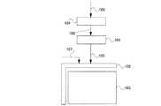
なお、表示装置とは、表示素子を有する装置のことを言う。なお、表示装置は、表示素子を含む複数の画素を含んでいても良い。なお、表示装置は、複数の画素を駆動させる周辺駆動回路を含んでいても良い。なお、複数の画素を駆動させる周辺駆動回路は、複数の画素と同一基板上に形成されてもよい。なお、表示装置は、ワイヤボンディングやバンプなどによって基板上に配置された周辺駆動回路、いわゆる、チップオングラス(COG)で接続されたICチップ、または、TABなどで接続されたICチップを含んでいても良い。なお、表示装置は、ICチップ、抵抗素子、容量素子、インダクタ、トランジスタなどが取り付けられたフレキシブルプリントサーキット(FPC)を含んでもよい。なお、表示装置は、フレキシブルプリントサーキット(FPC)などを介して接続され、ICチップ、抵抗素子、容量素子、インダクタ、トランジスタなどが取り付けられたプリント配線基盤(PWB)を含んでいても良い。なお、表示装置は、偏光板または位相差板などの光学シートを含んでいても良い。なお、表示装置は、照明装置、筐体、音声入出力装置、光センサなどを含んでいても良い。ここで、バックライトユニットのような照明装置は、導光板、プリズムシート、拡散シート、反射シート、光源(LED、冷陰極管など)、冷却装置(水冷式、空冷式)などを含んでいても良い。 Note that a display device refers to a device having a display element. Note that the display device may include a plurality of pixels including a display element. Note that the display device may include a peripheral driver circuit that drives a plurality of pixels. Note that the peripheral driver circuit that drives the plurality of pixels may be formed over the same substrate as the plurality of pixels. Note that the display device includes a peripheral drive circuit arranged on the substrate by wire bonding or bumps, an IC chip connected by so-called chip on glass (COG), or an IC chip connected by TAB or the like. May be. Note that the display device may include a flexible printed circuit (FPC) to which an IC chip, a resistor element, a capacitor element, an inductor, a transistor, and the like are attached. Note that the display device may include a printed wiring board (PWB) connected via a flexible printed circuit (FPC) or the like to which an IC chip, a resistor element, a capacitor element, an inductor, a transistor, or the like is attached. Note that the display device may include an optical sheet such as a polarizing plate or a retardation plate. Note that the display device may include a lighting device, a housing, a voice input / output device, an optical sensor, and the like. Here, the illumination device such as the backlight unit may include a light guide plate, a prism sheet, a diffusion sheet, a reflection sheet, a light source (LED, cold cathode tube, etc.), a cooling device (water cooling type, air cooling type) and the like. good.
なお、照明装置は、バックライトユニット、導光板、プリズムシート、拡散シート、反射シート、光源(LED、冷陰極管、熱陰極管など)、冷却装置などを有している装置のことをいう。 Note that the lighting device refers to a device including a backlight unit, a light guide plate, a prism sheet, a diffusion sheet, a reflective sheet, a light source (such as an LED, a cold cathode tube, a hot cathode tube), a cooling device, and the like.
なお、発光装置とは、発光素子などを有している装置のことをいう。表示素子として発光素子を有している場合は、発光装置は、表示装置の具体例の一つである。 Note that a light-emitting device refers to a device having a light-emitting element or the like. In the case where the display element includes a light-emitting element, the light-emitting device is one example of the display device.
なお、反射装置とは、光反射素子、光回折素子、光反射電極などを有している装置のことをいう。 In addition, a reflection apparatus means the apparatus which has a light reflection element, a light diffraction element, a light reflection electrode, etc.
なお、液晶表示装置とは、液晶素子を有している表示装置をいう。液晶表示装置には、直視型、投写型、透過型、反射型、半透過型などがある。 Note that a liquid crystal display device refers to a display device having a liquid crystal element. Liquid crystal display devices include direct view type, projection type, transmission type, reflection type, and transflective type.
なお、駆動装置とは、半導体素子、電気回路、電子回路を有する装置のことを言う。例えば、ソース信号線から画素内への信号の入力を制御するトランジスタ(選択用トランジスタ、スイッチング用トランジスタなどと呼ぶことがある)、画素電極に電圧または電流を供給するトランジスタ、発光素子に電圧または電流を供給するトランジスタなどは、駆動装置の一例である。さらに、ゲート信号線に信号を供給する回路(ゲートドライバ、ゲート線駆動回路などと呼ぶことがある)、ソース信号線に信号を供給する回路(ソースドライバ、ソース線駆動回路などと呼ぶことがある)などは、駆動装置の一例である。 Note that a driving device refers to a device having a semiconductor element, an electric circuit, and an electronic circuit. For example, a transistor that controls input of a signal from a source signal line into a pixel (sometimes referred to as a selection transistor or a switching transistor), a transistor that supplies voltage or current to a pixel electrode, or a voltage or current to a light-emitting element A transistor that supplies the voltage is an example of a driving device. Further, a circuit for supplying a signal to the gate signal line (sometimes referred to as a gate driver or a gate line driver circuit) and a circuit for supplying a signal to the source signal line (sometimes referred to as a source driver or source line driver circuit). ) Is an example of a driving device.
なお、表示装置、半導体装置、照明装置、冷却装置、発光装置、反射装置、駆動装置などは、互いに重複して有している場合がある。例えば、表示装置が、半導体装置および発光装置を有している場合がある。あるいは、半導体装置が、表示装置および駆動装置を有している場合がある。 Note that a display device, a semiconductor device, a lighting device, a cooling device, a light-emitting device, a reflecting device, a driving device, and the like may overlap with each other. For example, the display device may include a semiconductor device and a light-emitting device. Alternatively, the semiconductor device may include a display device and a driving device.
なお、Aの上にBが形成されている、あるいは、A上にBが形成されている、と明示的に記載する場合は、Aの上にBが直接接して形成されていることに限定されない。直接接してはいない場合、つまり、AとBと間に別の対象物が介在する場合も含むものとする。ここで、A、Bは、対象物(例えば、装置、素子、回路、配線、電極、端子、導電膜、層、など)であるとする。In addition, when it is explicitly described that B is formed on A or B is formed on A, it is limited that B is formed in direct contact with A. Not. The case where it is not in direct contact, that is, the case where another object is interposed between A and B is also included. Here, A and B are objects (for example, devices, elements, circuits, wirings, electrodes, terminals, conductive films, layers, etc.).
従って例えば、層Aの上に(もしくは層A上に)、層Bが形成されている、と明示的に記載されている場合は、層Aの上に直接接して層Bが形成されている場合と、層Aの上に直接接して別の層(例えば層Cや層Dなど)が形成されていて、その上に直接接して層Bが形成されている場合とを含むものとする。なお、別の層(例えば層Cや層Dなど)は、単層でもよいし、複層でもよい。Therefore, for example, when it is explicitly described that the layer B is formed on the layer A (or on the layer A), the layer B is formed in direct contact with the layer A. And the case where another layer (for example, layer C or layer D) is formed in direct contact with the layer A, and the layer B is formed in direct contact therewith. Note that another layer (for example, the layer C or the layer D) may be a single layer or a multilayer.
さらに、Aの上方にBが形成されている、と明示的に記載されている場合についても同様であり、Aの上にBが直接接していることに限定されず、AとBとの間に別の対象物が介在する場合も含むものとする。従って例えば、層Aの上方に、層Bが形成されている、という場合は、層Aの上に直接接して層Bが形成されている場合と、層Aの上に直接接して別の層(例えば層Cや層Dなど)が形成されていて、その上に直接接して層Bが形成されている場合とを含むものとする。なお、別の層(例えば層Cや層Dなど)は、単層でもよいし、複層でもよい。Furthermore, the same applies to the case where B is explicitly described as being formed above A, and is not limited to the direct contact of B on A. This includes the case where another object is interposed in. Therefore, for example, when the layer B is formed above the layer A, the case where the layer B is formed in direct contact with the layer A and the case where another layer is formed in direct contact with the layer A. (For example, the layer C or the layer D) is formed, and the layer B is formed in direct contact therewith. Note that another layer (for example, the layer C or the layer D) may be a single layer or a multilayer.
なお、Aの上にBが直接接して形成されている、と明示的に記載する場合は、Aの上に直接接してBが形成されている場合を含み、AとBと間に別の対象物が介在する場合は含まないものとする。 In addition, when it is explicitly described that B is formed in direct contact with A, it includes a case in which B is formed in direct contact with A. It shall not be included when an object is present.
なお、Aの下にBが、あるいは、Aの下方にBが、の場合についても、同様である。 The same applies to the case where B is below A or B is below A.
なお、明示的に単数として記載されているものについては、単数であることが望ましい。ただし、これに限定されず、複数であることも可能である。同様に、明示的に複数として記載されているものについては、複数であることが望ましい。ただし、これに限定されず、単数であることも可能である。In addition, about what is explicitly described as singular, it is preferable that it is singular. However, the present invention is not limited to this, and a plurality of them is also possible. Similarly, a plurality that is explicitly described as a plurality is preferably a plurality. However, the present invention is not limited to this, and the number can be singular.
本発明により、液晶分子を倒して配向する向きを増やすことによる視認者の視野角特性の向上に加え、各フレーム毎の液晶分子の透過率の変動による視野角特性の向上を図ることができる。その結果、視野角特性を向上させることができる液晶表示装置、及び当該液晶表示装置の駆動方法並びに当該液晶表示装置を具備する電子機器を提供することができる。According to the present invention, in addition to improving the viewing angle characteristics of the viewer by tilting the liquid crystal molecules and increasing the orientation, the viewing angle characteristics can be improved by changing the transmittance of the liquid crystal molecules for each frame. As a result, a liquid crystal display device capable of improving viewing angle characteristics, a driving method of the liquid crystal display device, and an electronic apparatus including the liquid crystal display device can be provided.
また本発明により、液晶分子を倒して配向する向きを増やすことによる視認者の視野角特性の向上に加え、隣接する画素毎の液晶分子の透過率の変動による視覚の錯覚を利用した視野角特性の向上を図ることができる。その結果、視野角特性を向上させることができる液晶表示装置、及び当該液晶表示装置の駆動方法並びに当該液晶表示装置を具備する電子機器を提供することができる。Further, according to the present invention, in addition to improving the viewing angle characteristics of the viewer by increasing the orientation direction by tilting the liquid crystal molecules, the viewing angle characteristics utilizing the visual illusion due to the variation in the transmittance of the liquid crystal molecules for each adjacent pixel Can be improved. As a result, a liquid crystal display device capable of improving viewing angle characteristics, a driving method of the liquid crystal display device, and an electronic apparatus including the liquid crystal display device can be provided.
以下、本発明の実施の形態について図面を参照しながら説明する。ただし、本発明は多くの異なる態様で実施することが可能であり、本発明の趣旨及びその範囲から逸脱することなくその形態及び詳細を様々に変更し得ることは当業者であれば容易に理解される。したがって、本実施の形態の記載内容に限定して解釈されるものではない。なお、本明細書中の図面において、同一部分または同様な機能を有する部分には同一の符号を付し、その説明は省略する。
(実施の形態1)Hereinafter, embodiments of the present invention will be described with reference to the drawings. However, the present invention can be implemented in many different modes, and those skilled in the art can easily understand that the modes and details can be variously changed without departing from the spirit and scope of the present invention. Is done. Therefore, the present invention is not construed as being limited to the description of this embodiment mode. Note that in the drawings in this specification, the same portions or portions having similar functions are denoted by the same reference numerals, and description thereof is omitted.
(Embodiment 1)
まず始めに、本発明を説明する上での基本原理について詳述する。First, the basic principle for explaining the present invention will be described in detail.
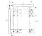
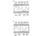
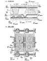
表示装置の表示部には、複数の画素が配置されており、一例として、図75に示すようにマトリクス状に配置されている。図75で、表示部7501には、走査線7502及び信号線7503に接続された画素7504が複数設けられている。ひとつの画素(以下、1画素という)は、1以上の複数の領域(サブ画素、サブピクセル、副画素ともいう。以下、サブ画素という)を有している。一例として1画素は、図75に示すように、第1のサブ画素(サブ画素A7504A)、第2のサブ画素(サブ画素B7504B)を有している。In the display portion of the display device, a plurality of pixels are arranged, and as an example, they are arranged in a matrix as shown in FIG. In FIG. 75, the
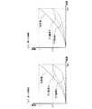
1画素は、サブ画素A、サブ画素Bそれぞれの光の透過量の総和により、1画素の階調を表現している。すなわち、1画素で表現する階調数に応じた光の透過量をXとすると、透過量Xは、サブ画素Aでの光の透過量XAと、サブ画素Bの光の透過量XBとの和になる。そして、サブ画素Aの透過量XA及びサブ画素Bの透過量XBの総和によって、透過量Xが制御されて、1画素の階調は表現されることとなる。One pixel expresses the gradation of one pixel by the total light transmission amount of each of the sub-pixel A and the sub-pixel B. That is, if the light transmission amount corresponding to the number of gradations expressed by one pixel is X, the transmission amount X is the light transmission amount XA of the subpixel A and the light transmission amount XB of the subpixel B. Become sum. Then, the transmission amount X is controlled by the sum of the transmission amount XA of the sub-pixel A and the transmission amount XB of the sub-pixel B, and the gradation of one pixel is expressed.
なお、画素またはサブ画素における光の透過量は、画素またはサブ画素の輝度であってもよい。また、画素またはサブ画素の光の反射量であってもよい。また、画素またはサブ画素の光の透過量と、画素またはサブ画素の光の反射量の和であってもよい。Note that the light transmission amount in the pixel or sub-pixel may be the luminance of the pixel or sub-pixel. Further, it may be the amount of reflected light of the pixel or sub-pixel. Further, it may be the sum of the light transmission amount of the pixel or sub-pixel and the light reflection amount of the pixel or sub-pixel.
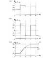
具体的な1画素の光の透過量とサブ画素A及びサブ画素Bの光の透過量について、図76(a)に例を挙げて説明する。図76(a)では、1画素での階調に対する、サブ画素Aの光の透過量7701、サブ画素Bの光の透過量7702、及び一画素での光の透過量の合算値7703について示した図である。例えば図76(a)に示すように、ある1画素での光の透過量が5のとき、サブ画素Aでの光の透過量を2、サブ画素Bでの光の透過量を3とすることで、合算値が5となり、1画素での光の透過量を5とすることができる。また、ある1画素での光の透過量が10のとき、サブ画素Aでの光の透過量を4、サブ画素Bでの光の透過量を6とすることで、合算値が10となり、1画素での光の透過量を10とすることができる。このように1画素の光の透過量に応じて、複数のサブ画素の光の透過量を変化させることで、適切に階調を表現することができる。A specific light transmission amount of one pixel and light transmission amounts of the sub-pixel A and the sub-pixel B will be described with reference to FIG. 76A. FIG. 76A shows a
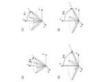
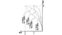
このとき、サブ画素Aとサブ画素Bとでは、液晶分子の配向状態を異なるようにできる。一例としては、図76(b)に示すようにサブ画素Aの液晶分子をθAだけ傾けて配向させ、図76(c)に示すようにサブ画素Bの液晶分子をθBだけ傾けて配向させる。そのため、光が透過される表示部(画面ともいう)に対し視認者が見る方角を変えたとき、視認者の目に認識される階調と実際表示される階調の変化量を少なくすることができる。そのため、視認者の視野角特性を改善することができる。At this time, the alignment state of the liquid crystal molecules can be different between the sub-pixel A and the sub-pixel B. As an example, the liquid crystal molecules of the sub-pixel A are tilted by θA as shown in FIG. 76B, and the liquid crystal molecules of the sub-pixel B are tilted by θB as shown in FIG. 76C. For this reason, when the viewing direction of the viewer changes with respect to a display portion (also referred to as a screen) through which light is transmitted, the amount of change between the gradation recognized by the viewer's eyes and the gradation actually displayed is reduced. Can do. Therefore, the viewing angle characteristics of the viewer can be improved.
以上説明したように、1画素の階調表現について、サブ画素に分割することによって視野角を広くすることができるが、ある画素での光の透過量が決まったとき、サブ画素Aでの光の透過量とサブ画素Bでの光の透過量とが固定されてしまうと、ある特定の方角から画面を見た場合に、階調が変化してしまう。As described above, with regard to the gradation expression of one pixel, the viewing angle can be widened by dividing it into sub-pixels. However, when the amount of light transmission in a certain pixel is determined, the light in the sub-pixel A If the transmission amount of light and the transmission amount of light in the sub-pixel B are fixed, the gradation changes when the screen is viewed from a specific direction.
そこで前述の階調の変化を鑑み、本実施形態で説明する構成は、ある画素での光の透過量が決まったとき、サブ画素Aでの光の透過量とサブ画素Bでの光の透過量とが固定されないようにするものである。サブ画素Aでの光の透過量とサブ画素Bでの光の透過量とが固定されないようにすることにより、ある特定の方角から画面を見た場合に、階調が変化してしまうのをさらに低減することができる。Therefore, in view of the change in gradation described above, the configuration described in this embodiment is configured such that when the amount of light transmitted through a certain pixel is determined, the amount of light transmitted through sub-pixel A and the light transmitted through sub-pixel B. The amount is not fixed. By preventing the light transmission amount at the sub-pixel A and the light transmission amount at the sub-pixel B from being fixed, the gradation changes when the screen is viewed from a specific direction. Further reduction can be achieved.
本実施形態で説明する構成では、1画素での光の透過量Xのとき、サブ画素Aでの光の透過量XAと、サブ画素Bの光の透過量XBとは、複数の組み合わせを取ることができることに着目し、着想に至ったものである。すなわち、1画素での光の透過量を決める、サブ画素Aでの光の透過量及びサブ画素Bでの光の透過量の組み合わせを複数組用いるものである。その結果、1画素での光の透過量を決める各サブ画素での光の透過量が固定されることなく、ある特定の方角から画面を見た場合の階調の変化を低減することができる。In the configuration described in the present embodiment, when the light transmission amount X is 1 pixel, the light transmission amount XA of the sub-pixel A and the light transmission amount XB of the sub-pixel B take a plurality of combinations. Focusing on being able to do it, it came to an idea. That is, a plurality of combinations of the light transmission amount in the sub-pixel A and the light transmission amount in the sub-pixel B, which determine the light transmission amount in one pixel, are used. As a result, the change in gradation when the screen is viewed from a specific direction can be reduced without fixing the light transmission amount in each sub-pixel that determines the light transmission amount in one pixel. .
例えば、1画素での光の透過量Xが5のとき、サブ画素Aでの光の透過量XA=1、サブ画素Bでの光の透過量XB=4とする組み合わせがある。あるいは、サブ画素Aでの光の透過量XA=0、サブ画素Bでの光の透過量XB=5とする組み合わせがある。あるいは、サブ画素Aでの光の透過量XA=3、サブ画素Bでの光の透過量XB=2とする組み合わせがある。すなわちサブ画素A及びサブ画素Bの光の透過量を(XA、XB)として表現したとき、1画素での光の透過量Xが5の場合は、(0,5)、(1,4)、(2,3)、(3,2)などのように、複数の組み合わせを取ることができる。なお、透過量XAと透過量XBとの総和は、光の透過量Xとなる。For example, when the light transmission amount X in one pixel is 5, there is a combination in which the light transmission amount XA = 1 in the sub-pixel A and the light transmission amount XB = 4 in the sub-pixel B. Alternatively, there is a combination in which the light transmission amount XA = 0 in the sub-pixel A and the light transmission amount XB = 5 in the sub-pixel B. Alternatively, there is a combination in which the light transmission amount XA = 3 in the sub-pixel A and the light transmission amount XB = 2 in the sub-pixel B. That is, when the light transmission amount of the sub-pixel A and the sub-pixel B is expressed as (XA, XB), when the light transmission amount X of one pixel is 5, (0, 5), (1, 4) , (2, 3), (3, 2), etc., a plurality of combinations can be taken. Note that the sum of the transmission amount XA and the transmission amount XB is the light transmission amount X.
具体的な構成としては、所望の階調を得る上で、1画素での光の透過量Xが必要なときに、複数の(XA、XB)の組み合わせを用いるものである。例えば、ある期間(以下、第1の期間という)において、(XA1、XB1)とし、別の期間(以下、第2の期間)では、(XA2、XB2)とする。その結果、第1の期間と第2の期間を併せたトータルの期間では、第1の期間及び第2の期間により光の透過量が平均化され、ある特定の方角から画面を見た場合にも、階調が変化してしまうのを低減することができる。As a specific configuration, a combination of a plurality of (XA, XB) is used when a light transmission amount X in one pixel is necessary to obtain a desired gradation. For example, (XA1, XB1) is set in a certain period (hereinafter referred to as a first period), and (XA2, XB2) is set in another period (hereinafter referred to as a second period). As a result, in the total period including the first period and the second period, the amount of transmitted light is averaged by the first period and the second period, and the screen is viewed from a specific direction. However, the change in gradation can be reduced.
なお上述の説明では1画素の光の透過量X、サブ画素Aの光の透過量XA及びサブ画素Bの光の透過量XBの関係について、X=XA+XBであるものとして説明したが、これに限定されない。XAとXBの和が、Xと概ね一致していればよい。X、XA、XBは、見る方角によって、透過量が多少変化するため、XAとXBの和と、Xとでは、ずれが生じる場合がある。ただし、人間の目でみて、ちらつきが出たり、正常な階調に見えなかったりするような問題が生じなければ、問題はない。Xに対するXAとXBの和のばらつきは、概略で、10%程度、より望ましくは5%程度あってもよい。In the above description, the relationship between the light transmission amount X of one pixel, the light transmission amount XA of the sub-pixel A, and the light transmission amount XB of the sub-pixel B is described as X = XA + XB. It is not limited. It is only necessary that the sum of XA and XB substantially coincides with X. Since X, XA, and XB slightly change the amount of transmission depending on the viewing direction, there may be a deviation between the sum of XA and XB and X. However, there is no problem unless a problem such as flickering or normal gradation does not occur with the human eye. The variation of the sum of XA and XB with respect to X may be roughly about 10%, more preferably about 5%.
次に、光の透過量とは別のパラメータを用いる構成について説明し、当該別のパラメータと光の透過量との関係について述べる。すなわち、光の透過量とは別のパラメータを用いて、1画素の光の透過量を制御して、階調を制御する例について説明する。Next, a configuration using a parameter different from the light transmission amount will be described, and the relationship between the another parameter and the light transmission amount will be described. That is, an example in which the gradation is controlled by controlling the light transmission amount of one pixel using a parameter different from the light transmission amount will be described.
一例として、サブ画素Aでの光の透過領域の面積SA、サブ画素Bでの光の透過領域の面積SBとし、サブ画素Aでの単位面積かつ単位時間あたりの光の透過量TA、サブ画素Bでの単位面積かつ単位時間あたりの光の透過量TBとし、サブ画素Aでの光の透過時間をPA、サブ画素Bでの光の透過時間をPBとする。前述のパラメータを用いて、サブ画素Aの光の透過量XA及びサブ画素Bの光の透過量XBを述べると、XA=SA×TA×PA、およびXB=SB×TB×PB、の関係が成り立つ。よって、光の透過領域の面積、単位面積かつ単位時間当たりの光の透過量、及び光の透過時間などパラメータに関して、少なくとも1つのパラメータを制御して、光の透過量を制御できる。As an example, the area SA of the light transmission region in the sub-pixel A, the area SB of the light transmission region in the sub-pixel B, the light transmission amount TA per unit area and unit time in the sub-pixel A, the sub-pixel The light transmission amount TB per unit area and unit time in B is set as PA, the light transmission time in the sub-pixel A is PA, and the light transmission time in the sub-pixel B is PB. Using the aforementioned parameters, the light transmission amount XA of the sub-pixel A and the light transmission amount XB of the sub-pixel B are described. The relationship of XA = SA × TA × PA and XB = SB × TB × PB is obtained. It holds. Therefore, it is possible to control the light transmission amount by controlling at least one parameter regarding parameters such as the area of the light transmission region, the light transmission amount per unit area and unit time, and the light transmission time.
なお、画素またはサブ画素における光の透過領域は、画素またはサブ画素の発光領域、または画素またはサブ画素の光の反射領域であってもよい。また、画素またはサブ画素における光の透過領域は、画素またはサブ画素の光の透過領域と、画素またはサブ画素の光の反射領域の和であってもよい。また、画素またはサブ画素での単位面積かつ単位時間あたりの光の透過量は、画素またはサブ画素の単位時間あたりの発光輝度、または画素またはサブ画素の単位時間あたりの光の反射量であってもよい。また、画素またはサブ画素での単位面積かつ単位時間あたりの光の透過量は、画素またはサブ画素での単位面積かつ単位時間あたりの光の透過量と、画素またはサブ画素での単位面積かつ単位時間あたりの光の反射量の和であってもよい。また、画素またはサブ画素での光の透過時間は、画素またはサブ画素の発光時間、または画素またはサブ画素の光の反射時間であってもよい。また、画素またはサブ画素での光の透過時間は、画素またはサブ画素の光の透過時間と、画素またはサブ画素の光の反射時間の和であってもよい。Note that the light transmission region in the pixel or sub-pixel may be a light-emitting region of the pixel or sub-pixel or a light reflection region of the pixel or sub-pixel. Further, the light transmission region in the pixel or sub-pixel may be the sum of the light transmission region of the pixel or sub-pixel and the light reflection region of the pixel or sub-pixel. The amount of light transmitted per unit area and unit time in the pixel or sub-pixel is the light emission luminance per unit time of the pixel or sub-pixel or the amount of light reflection per unit time of the pixel or sub-pixel. Also good. The light transmission amount per unit area and unit time in the pixel or sub-pixel includes the unit area and light transmission amount per unit time in the pixel or sub-pixel, and the unit area and unit in the pixel or sub-pixel. It may be the sum of the amount of reflected light per hour. The light transmission time in the pixel or sub-pixel may be the light emission time of the pixel or sub-pixel or the light reflection time of the pixel or sub-pixel. The light transmission time in the pixel or sub-pixel may be the sum of the light transmission time of the pixel or sub-pixel and the light reflection time of the pixel or sub-pixel.
また、各サブ画素での単位面積かつ単位時間当たりの光の透過量TA、TBは、サブ画素に加えられる階調信号によって制御することができる。したがって、サブ画素Aでの階調信号がEAのとき、単位面積かつ単位時間当たりの光の透過量TAとなり、サブ画素Bでの階調信号EBのとき、単位面積かつ単位時間当たりの光の透過量TB、とすることができる。The light transmission amounts TA and TB per unit area and unit time in each sub-pixel can be controlled by a gradation signal applied to the sub-pixel. Therefore, when the gradation signal in the sub-pixel A is EA, the light transmission amount TA per unit area and unit time is obtained, and in the case of the gradation signal EB in the sub-pixel B, the light intensity per unit area and unit time is obtained. Transmission amount TB.
また、各サブ画素での単位面積かつ単位時間当たりの光の透過量TA、TBは、階調信号に応じて実際の表示素子に加える信号によって決めることができる。一例として、液晶素子の場合、サブ画素Aでの階調信号EAの場合、サブ画素Aの画素電極に加える階調電圧VAは、液晶素子の特性に合わせて、ガンマ補正された値となっている。また、液晶素子は、交流駆動されるため、正極用の電圧と負極用の電圧とが必要となる。コモン電極の電位を0Vだとすると、正極用の階調電圧VA、負極用の階調電圧−VAが画素電極に加えられる。その結果、単位面積かつ単位時間当たりの透過量TAを制御して、透過量XAを制御することができる。なお、サブ画素Bの場合も同様である。The light transmission amounts TA and TB per unit area and unit time in each sub-pixel can be determined by a signal applied to an actual display element in accordance with a gradation signal. As an example, in the case of the liquid crystal element, in the case of the gradation signal EA in the sub-pixel A, the gradation voltage VA applied to the pixel electrode of the sub-pixel A is a value that is gamma-corrected according to the characteristics of the liquid crystal element. Yes. Further, since the liquid crystal element is AC driven, a positive voltage and a negative voltage are required. Assuming that the potential of the common electrode is 0 V, the gradation voltage VA for positive electrode and the gradation voltage -VA for negative electrode are applied to the pixel electrode. As a result, the transmission amount XA can be controlled by controlling the transmission amount TA per unit area and unit time. The same applies to the sub-pixel B.
なお、階調電圧は、サブ画素の透過領域の面積、光の透過時間、またはバックライト等の輝度等を考慮した上での値となっている。例えば、光の透過領域の面積が、サブ画素A:サブ画素B=1:2となっている場合は、光の透過量(XA、XB)が(2,4)となっていても、サブ画素Aとサブ画素Bには、同じ階調電圧が供給されることになる。なぜなら、同じ階調電圧でも、透過領域の面積が異なるため、結果的に光の透過量も異なるためである。Note that the gradation voltage is a value in consideration of the area of the transmission region of the sub-pixel, the light transmission time, the luminance of the backlight, or the like. For example, when the area of the light transmission region is subpixel A: subpixel B = 1: 2, even if the light transmission amount (XA, XB) is (2, 4), The same gradation voltage is supplied to the pixel A and the sub-pixel B. This is because, even with the same gradation voltage, the areas of the transmission regions are different, resulting in different amounts of light transmission.
なお、コモン電極の電位を0Vと仮定した場合について述べたが、これに限定されない。コモン電極の電位が0V以外の場合、それに応じて、正極用と負極用の階調電圧もシフトされることとなる。また、コモン電極の電位が0Vの場合であっても、正極用の階調電圧と負極用の階調電圧とは、絶対値が等しいとは限らない。ノイズなどの影響により、正極用の階調電圧と負極用の階調電圧とでずれが生じる場合がある。Although the case where the potential of the common electrode is assumed to be 0 V has been described, the present invention is not limited to this. When the potential of the common electrode is other than 0V, the gradation voltages for the positive electrode and the negative electrode are also shifted accordingly. Even when the potential of the common electrode is 0 V, the absolute value of the positive gradation voltage and the negative gradation voltage are not necessarily the same. Due to the influence of noise or the like, there may be a difference between the gradation voltage for the positive electrode and the gradation voltage for the negative electrode.
また、液晶素子を用いた表示装置の場合、バックライトやフロントライトなどから光が照射され、光を透過する割合を液晶素子で制御している。つまり、液晶素子で、光の透過率を制御しているということができる。したがって、単位面積かつ単位時間当たりの透過量、透過量などは、バックライトやフロントライトなどによって照射される光の強度と、液晶素子での光の透過率とを用いて制御することができる。In the case of a display device using a liquid crystal element, light is irradiated from a backlight, a front light, or the like, and the ratio of transmitting light is controlled by the liquid crystal element. That is, it can be said that the light transmittance is controlled by the liquid crystal element. Therefore, the amount of transmission per unit area and per unit time, the amount of transmission, and the like can be controlled using the intensity of light irradiated by a backlight, a front light, and the like and the light transmittance of the liquid crystal element.
上述のように、さまざまなパラメータを用いて、光の透過量を制御することができる。上述のパラメータのうち、どのパラメータを用いて制御するかは、任意に決定することができる。また、パラメータは、上記説明した光の透過領域の面積、単位面積かつ単位時間当たりの光の透過量、及び光の透過時間などパラメータに限定されず、光の透過量を制御できるパラメータであれば、様々なパラメータを用いることができる。As described above, the amount of light transmission can be controlled using various parameters. Of the above parameters, which parameter is used for control can be arbitrarily determined. The parameters are not limited to the parameters such as the area of the light transmission region described above, the light transmission amount per unit area and unit time, and the light transmission time, and may be any parameters that can control the light transmission amount. Various parameters can be used.
そして、1画素での光の透過量Xが必要なときには、各サブ画素での光の透過量に応じたパラメータの複数の組み合わせを用いる。光の透過量は、透過領域の面積、単位面積かつ単位時間当たりの光の透過量、光の透過時間、階調信号、階調電圧、透過率、バックライト等の輝度などのパラメータによって制御されるため、これらのパラメータより、少なくとも1つのパラメータを選択する。そして、そのパラメータにおいて、値の組み合わせを複数個用いて、一画素での光の透過量Xを制御する。光の透過量を制御するために用いるパラメータは、1つである方が制御しやすいため望ましい。ただし、これに限定されず、複数のパラメータを用いて、それらの組み合わせてもよい。When a light transmission amount X in one pixel is required, a plurality of combinations of parameters corresponding to the light transmission amount in each sub-pixel is used. The light transmission amount is controlled by parameters such as the area of the transmission region, the light transmission amount per unit area and unit time, the light transmission time, the gradation signal, the gradation voltage, the transmittance, and the luminance such as the backlight. Therefore, at least one parameter is selected from these parameters. In the parameter, a plurality of combinations of values are used to control the light transmission amount X in one pixel. It is desirable that one parameter is used for controlling the light transmission amount because it is easier to control. However, the present invention is not limited to this, and a plurality of parameters may be used to combine them.
例えば、サブ画素Aとサブ画素Bとがある場合、パラメータとしてサブ画素Aの階調信号EA、サブ画素Aの透過時間PA、サブ画素Bの階調信号EB、及びサブ画素Bの透過時間PBを用い、(EA、PA、EB、PB)という値の組を複数個用意して、光の透過量Xを制御してもよい。あるいは、パラメータとしてサブ画素Aの階調信号EA、サブ画素Bの階調信号EBを用いて、(EA、EB)という値の組を複数個用いて、光の透過量Xを制御してもよい。また1画素を構成するサブ画素数が2個以外の場合も、同様にすることができる。For example, when there are sub-pixel A and sub-pixel B, the gradation signal EA of sub-pixel A, transmission time PA of sub-pixel A, gradation signal EB of sub-pixel B, and transmission time PB of sub-pixel B are used as parameters. The light transmission amount X may be controlled by preparing a plurality of sets of values (EA, PA, EB, PB). Alternatively, the light transmission amount X may be controlled by using a plurality of sets of values (EA, EB) using the gradation signal EA of the sub-pixel A and the gradation signal EB of the sub-pixel B as parameters. Good. The same can be done when the number of sub-pixels constituting one pixel is other than two.
なお、光の透過量、光の透過領域の面積、単位面積かつ単位時間当たりの光の透過量、光の透過時間、階調信号、階調電圧、透過率、バックライト等の輝度などは、アナログ量でもよいし、デジタル量でもよい。表示装置内でガンマ補正が行われ、かつ、液晶素子の交流駆動が考慮されている場合は、階調電圧は、アナログ量であることが望ましい。一方、階調信号が、ガンマ補正や液晶素子の交流駆動に関する情報を有していない場合は、階調信号は、デジタル量の信号(以下、デジタル信号という)であることが望ましい。デジタル信号であれば、信号の保持や信号の処理が容易にできるため、階調信号はデジタル信号であることが望ましい。したがって、最初は、デジタル信号であり、表示部の液晶素子に信号を加える直前に、アナログ量の信号(以下、アナログ信号という)に変換されることが望ましい。このようなデジタル−アナログ変換が行われるときに、ガンマ補正や液晶素子の交流駆動に関する情報が追加されることで、効率のよい階調信号の表示部への入力を行うことができる。The light transmission amount, the area of the light transmission region, the light transmission amount per unit area and unit time, the light transmission time, the gradation signal, the gradation voltage, the transmittance, the brightness of the backlight, etc. It may be an analog quantity or a digital quantity. When gamma correction is performed in the display device and AC driving of the liquid crystal element is taken into consideration, the gradation voltage is desirably an analog amount. On the other hand, when the gradation signal does not have information regarding gamma correction or AC drive of the liquid crystal element, the gradation signal is preferably a digital signal (hereinafter referred to as a digital signal). Since a digital signal can easily hold and process a signal, the gradation signal is preferably a digital signal. Therefore, the digital signal is initially converted to an analog signal (hereinafter referred to as an analog signal) immediately before the signal is applied to the liquid crystal element of the display unit. When such digital-analog conversion is performed, information relating to gamma correction and AC drive of the liquid crystal element is added, so that an efficient gradation signal can be input to the display unit.
なお、1画素での光の透過量Xが必要なときに、例えば、サブ画素Aとサブ画素Bとがある場合において、サブ画素Aの光の透過量XA及びサブ画素Bの光の透過量XBの組み合わせ(XA、XB)を用いる場合、(XA、XB)の複数の組み合わせの各々は、データとしてあらかじめ用意されていてもよいし、随時、計算することなどによって作成されてもよいし、一部があらかじめ用意されていて、一部が計算によって作成されてもよい。When a light transmission amount X in one pixel is necessary, for example, when there are sub-pixel A and sub-pixel B, light transmission amount XA of sub-pixel A and light transmission amount of sub-pixel B When using a combination of XB (XA, XB), each of the plurality of combinations of (XA, XB) may be prepared in advance as data, or may be created by calculation, etc. A part may be prepared in advance, and a part may be created by calculation.
なお、複数の(XA、XB)の組み合わせを用いる場合、どの順序または期間で当該組み合わせのデータを用いるかについては、特に限定されない。例えば、複数の(XA、XB)の組み合わせを、データとしてあらかじめ記憶部に用意されていてもよい、また複数の(XA、XB)の組み合わせを演算部で、随時、演算処理することによって作成してもよい。また、複数の(XA、XB)の組み合わせの一部をあらかじめ記憶部に用意し、一部を演算部で演算処理することによって作成してもよい。Note that in the case of using a combination of a plurality of (XA, XB), there is no particular limitation on which order or period the data of the combination is used. For example, a combination of a plurality of (XA, XB) may be prepared in advance in the storage unit as data, or a combination of a plurality of (XA, XB) is created by performing arithmetic processing at any time in the arithmetic unit. May be. Alternatively, a part of a plurality of (XA, XB) combinations may be prepared in advance in the storage unit, and a part of the combination may be calculated by the calculation unit.
なお、あらかじめ複数の(XA、XB)の組み合わせのデータが記憶部に用意されている場合は、例えば、1画素での光の透過量Xが5のとき、(XA、XB)の組み合わせは(0,5)、(1,4)、(2,3)、(3,2)の合計4つの組み合わせを用いるとして、4つ分のデータを用意しておいてもよい。データを用意しておく場合は、記憶部にルックアップテーブル(look up table:LUT)としてデータを保存すればよい。つまり、透過量Xのとき、それに応じた(XA、XB)を、ルックアップテーブルとしてデータを記憶しておき、ルックアップテーブルを参照して随時読み出すことによって、複数の(XA、XB)の組み合わせを用いても良い。If a plurality of (XA, XB) combination data is prepared in the storage unit in advance, for example, when the light transmission amount X in one pixel is 5, the combination of (XA, XB) is ( Assuming that a total of four combinations of (0,5), (1,4), (2,3), and (3,2) are used, four pieces of data may be prepared. When data is prepared, the data may be stored in the storage unit as a look-up table (LUT). That is, when the transmission amount is X, (XA, XB) corresponding to the transmission amount X is stored as data as a lookup table, and is read out as needed with reference to the lookup table, thereby combining a plurality of (XA, XB). May be used.
なお、ルックアップテーブルとしてデータを記憶部に保存しておく場合、透過量、透過領域の面積、単位面積かつ単位時間当たりの光の透過量、光の透過時間、階調信号、階調電圧、透過率、バックライト等の輝度など、さまざまなパタメータに関して保存しておくことができる。ただし、通常、表示装置を設計した段階において、記憶部に保存するルックアップテーブルの仕様は、既に決まってしまうものもある。そのため、実際の表示に寄与しないパラメータについてはルックアップテーブルとして記憶部に保存しておく必要はない。When data is stored in the storage unit as a lookup table, the transmission amount, the area of the transmission region, the transmission amount of light per unit area and unit time, the transmission time of light, the gradation signal, the gradation voltage, Various parameters such as transmittance, brightness of backlight, etc. can be stored. However, in general, the specifications of the lookup table stored in the storage unit are already determined at the stage of designing the display device. Therefore, parameters that do not contribute to actual display need not be stored in the storage unit as a lookup table.
なお、ルックアップテーブルとして複数の組み合わせ(XA、XB)のデータが記憶部に保存されている場合、順番に複数の組み合わせ(XA、XB)を用いるようにすることが望ましい。それにより、全てに行き渡ってデータを用いることができ、視野角を広げることができる。例えば、1画素での光の透過量Xが5のとき、(XA、XB)の組み合わせとして、(0,5)、(1,4)、(2,3)、(3,2)の合計4つの組み合わせのデータがルックアップテーブルとして保存されている場合、(0,5)、(1,4)、(2,3)、(3,2)の順序でデータが用いられる。組み合わせ(3,2)が終了した場合は、組み合わせ(0,5)に戻り、さらに、同様に繰り返される。In addition, when data of a plurality of combinations (XA, XB) is stored in the storage unit as the lookup table, it is desirable to use a plurality of combinations (XA, XB) in order. Thereby, data can be used throughout, and the viewing angle can be widened. For example, when the light transmission amount X in one pixel is 5, the total of (0,5), (1,4), (2,3), (3,2) as a combination of (XA, XB) When four combinations of data are stored as a lookup table, the data is used in the order of (0, 5), (1, 4), (2, 3), (3, 2). When the combination (3, 2) is completed, the process returns to the combination (0, 5) and is repeated in the same manner.
ただし、前述した1画素での光の透過量Xを制御する組み合わせのデータ(以下、組み合わせデータという)の用いられ方は特に限定されない。どのような順序で組み合わせデータを用いるかについてのデータは、予めルックアップテーブルとともに記憶部へ保存しておいてもよい。そして、組み合わせデータの順序に関するデータは、記憶部より読み出して用いることができる。組み合わせデータを、ランダムな順序で用いても良い。ランダムな順序で組み合わせデータを用いる場合は、ルックアップテーブルよりデータを選択する際に、乱数を発生させて、乱数に応じた組み合わせデータを用いればよい。However, the method of using the combination data for controlling the light transmission amount X in one pixel (hereinafter referred to as combination data) is not particularly limited. Data regarding the order in which the combination data is used may be stored in the storage unit together with the lookup table. Data relating to the order of the combination data can be read from the storage unit and used. The combination data may be used in a random order. When using combination data in a random order, when selecting data from a lookup table, a random number may be generated and combination data corresponding to the random number may be used.
次に、1画素に複数のサブ画素を有し、サブ画素毎に光の透過量を制御する階調信号(以下、サブ階調信号ともいう)を、ルックアップテーブルにデータを保存しておく場合の具体的な構成例について述べる。Next, a gradation signal (hereinafter also referred to as a sub gradation signal) that has a plurality of sub pixels in one pixel and controls the light transmission amount for each sub pixel is stored in a lookup table. A specific configuration example will be described.
図1は、液晶表示装置のブロック図の構成例を示している。図1に示す液晶表示装置は、階調データ変換部101、駆動部102、表示部103、階調データ記憶部104を有している。FIG. 1 shows a configuration example of a block diagram of a liquid crystal display device. The liquid crystal display device illustrated in FIG. 1 includes a gradation
図1において、階調データ記憶部104には、階調信号100が入力されている。階調データ記憶部104は、入力される階調信号100の階調数に応じて、階調データ記憶部104に記憶されたルックアップテーブルを参照する。そして、階調データ記憶部104はルックアップテーブルに基づく組み合わせデータ106を階調データ変換部101に出力する。階調データ変換部101は、組み合わせデータ106に基づいたサブ階調信号105を駆動部102に出力する。また駆動部102には表示部103の表示を制御するための制御信号107が入力されている。駆動部102は、複数のサブ階調信号105及び制御信号107に基づいて、表示部103に表示を行うための信号を出力する。また駆動部102は、表示部103に出力する信号のD/A変換、ガンマ補正、及び極性反転を行う機能を有する。In FIG. 1, a
なお、サブ階調信号105は、表示部103の各画素に供給される画像データ(動画、静止画など)に対応する。また上述のように、表示部103の各画素は複数のサブ画素を有しており、サブ階調信号105は、各サブ画素の階調を制御するための信号である。また、制御信号107は、駆動部102を駆動するための、クロックパルス、スタートパルスなどの基準となる信号である。The
なお、階調信号100はデジタル信号であることが好ましい。階調信号100がデジタル信号であることによって、階調信号100の階調数に基づいた組み合わせデータ106への変換を階調データ記憶部104で容易に行うことができる。または、階調信号100の保持も容易に行うことができる。または、階調データ変換部101より駆動部102に出力されるサブ階調信号105は、デジタル信号であることが好ましい。サブ階調信号105がデジタル信号であることによって、ノイズの影響を受けにくい、正確な信号を転送することができる。そして、駆動部102において、デジタル信号は、ガンマ補正、極性の調整(正極信号または負極信号の選択)などが行われたアナログ信号に変換される。そして、アナログ信号が、表示部103の画素に供給される。Note that the
なお図1で説明した液晶表示装置のブロック図の構成は、階調信号100がデジタル信号である場合の一例について説明したが、本発明はこれに限定されるものではない。階調信号100がアナログ信号の場合には、図57に示すように、階調データ変換部101の階調信号入力側にA/D変換回路5701を設け、アナログ信号の階調信号100を適切なビット数のデジタル信号5702に変換すればよい。また、駆動部102にアナログ信号のサブ階調信号を出力する構成とする際には、図58に示すように、駆動部102のサブ階調信号が入力される側にD/A変換回路5801を設け、デジタル信号のサブ階調信号をアナログ信号5802に変換し、駆動部102に出力してもよい。なお、この場合、D/A変換回路5801において、ガンマ補正、極性の調整(正極信号または負極信号の選択)などが行われる場合が多い。よって、駆動部102では、そのような機能は省かれる場合が多い。駆動部102にアナログ信号を供給する場合、駆動部102の構成を簡略化することができるため、表示部103と駆動部102とが同じ基板上に形成されることが可能となる。これにより、狭額縁化、信頼性の向上、部品点数の低減などを実現することができる。Note that the configuration of the block diagram of the liquid crystal display device illustrated in FIG. 1 has been described with respect to an example in which the
なお、表示部103には、サブ階調信号105として、アナログ信号が供給される場合が多いが、これに限定されない。表示部103に、階調信号として、デジタル信号を供給し、時間階調方式や面積階調方式などを用いて表示してもよい。Note that an analog signal is often supplied to the
階調データ記憶部104からは階調データ変換部101より、階調信号100に対応した組み合わせデータ106が読み出される。なお、本実施の形態においては、階調信号の階調数をn階調(nは0を含む自然数)とする。そして階調データ記憶部104は階調数に対応した組み合わせデータ106をルックアップテーブルとして記憶しているものとして、以下説明していく。組み合わせデータ106は、階調信号100の階調数に基づいてルックアップテーブルを参照し、階調データ記憶部104より出力される。なお、ルックアップテーブルとは、階調信号100の階調数に対応して階調データ変換部101より出力するサブ階調信号105で表現される光の透過量を予め見積もったデータの配列のことである。The
ルックアップテーブルは、階調信号100の階調数に対応した組み合わせデータを有する。そして任意の異なる期間において、複数の組み合わせデータのうち、いずれか一つの組み合わせデータを選択し、階調信号100の階調数に応じた組み合わせデータ106を階調データ変換部101に出力する。The look-up table has combination data corresponding to the number of gradations of the
また、ルックアップテーブルには、それぞれ同じ階調信号100の階調数に対応した組み合わせデータを複数有する。図2では、階調データ記憶部104に記憶されるルックアップテーブルを模式的に示したものである。本実施の形態では、第1の期間では第1の組み合わせデータを階調データ変換部101に組み合わせデータ106として出力し、第2の期間では第2の組み合わせデータを階調データ変換部101に組み合わせデータ106として出力する。前述のように同じ階調信号100の階調数に対応した組み合わせデータであっても、第1の組み合わせデータからの組み合わせデータ及び第2の組み合わせデータからの組み合わせデータは、それぞれ異なる電圧のサブ階調信号105を階調データ変換部101にて生成する。The lookup table has a plurality of combination data corresponding to the number of gradations of the
また本実施の形態で説明する表示装置での表示部は、複数の画素を含んでおり、複数の画素のそれぞれは、ひとつの画素がサブ画素を有している。サブ画素のそれぞれは液晶素子を有している。サブ画素のそれぞれが有する液晶素子にはサブ階調信号105が供給される。通常は、視野角を広げるために、サブ画素ごとに異なる階調電圧が供給されており、液晶素子による光の透過率の制御している。ただし、これに限定されない。サブ画素のうちのいずれかに同じ大きさの階調電圧が供給される場合もある。複数の画素のそれぞれは、サブ画素毎に別の方向へ液晶分子を倒して配向する向きを増やすことで、視認者の視野角特性の向上を図り、表示装置に画像データに基づく表示を行わせている。本実施の形態では、一つの画素が、第1のサブ画素(サブ画素Aともいう)及び第2のサブ画素(サブ画素Bともいう)を有する構成として説明する。In addition, a display portion in the display device described in this embodiment includes a plurality of pixels, and each of the plurality of pixels has a single pixel. Each sub-pixel has a liquid crystal element. A
図2に示すルックアップテーブルは、サブ画素Aに入力するサブ階調信号(第1のサブ階調信号、またはサブ階調信号Aという:以下、サブ階調信号Aという)、及びサブ画素Bに入力するサブ階調信号(第2のサブ階調信号、またはサブ階調信号Bという:以下、サブ階調信号Bという)に対応した第1の組み合わせデータ201、を有する。また、サブ階調信号A及びサブ階調信号Bに対応した第2の組み合わせデータ202、を有する。なお、図2において、階調信号100の階調数が0のとき、第1の組み合わせデータ201として、サブ階調信号A及びサブ階調信号Bに対応した組み合わせデータ(a0,b0)、を参照し、第2の組み合わせデータ202として、サブ階調信号A及びサブ階調信号Bに対応した組み合わせデータ(c0,d0)、を参照するものである。同様にして、階調信号100の階調数が1乃至(n−1)のとき、第1の組み合わせデータ201は、サブ階調信号A及びサブ階調信号Bに対応した組み合わせデータ(a1,b1)乃至(a(n−1),b(n−1))、を参照し、第2の組み合わせデータ202では、サブ階調信号A及びサブ階調信号Bに対応した組み合わせデータ(c1,d1)乃至(c(n−1),d(n−1))、を参照するものである。The look-up table shown in FIG. 2 includes a sub gray level signal (first sub gray level signal or sub gray level signal A: hereinafter referred to as sub gray level signal A) input to the sub pixel A, and a sub pixel B. The
なお、図2に示すルックアップテーブルの例では、ある階調について2種類の組み合わせデータを有する場合について述べたが、これに限定されない。さらに、全ての階調数にわたって、組み合わせデータの種類数が同じである場合について述べたが、これに限定されない。階調信号100の階調数によって、組み合わせデータの種類数が異なっていても良い。例えば、ある特定の方角から画面を見た場合の階調の変化が大きい階調数においては、より多くの組み合わせデータをルックアップテーブルに有していても良い。それによって、ある特定の方角から画面を見た場合の階調のズレを低減し、視野角特性を向上させることができる。In the example of the lookup table shown in FIG. 2, the case where two types of combination data are provided for a certain gradation is described, but the present invention is not limited to this. Furthermore, although the case where the number of types of combination data is the same over the entire number of gradations has been described, the present invention is not limited to this. Depending on the number of gradations of the
上記示したサブ画素それぞれが有する液晶素子は2つの電極を有しており、例として、2つの電極の電位差が0Vのとき(以下、電圧停止時、又は電圧停止状態ともいう)には、透過率0%である(以下、ノーマリーブラックともいう)場合について述べている。なお、これに限らず、液晶素子には電圧停止時において透過率100%(以下、ノーマリーホワイトともいう)となる素子を用いても良い。The liquid crystal element included in each of the sub-pixels described above includes two electrodes. For example, when the potential difference between the two electrodes is 0 V (hereinafter, also referred to as a voltage stop state or a voltage stop state), transmission is performed. The case where the rate is 0% (hereinafter also referred to as normally black) is described. Note that the present invention is not limited to this, and an element having a transmittance of 100% (hereinafter also referred to as normally white) when the voltage is stopped may be used as the liquid crystal element.
ここで、上述の図1の各ブロックの動作、ルックアップテーブルの組み合わせデータについて、具体例を用いて述べる。なお、表示部103の画素は、例として、サブ画素A、及びサブ画素Bの2つのサブ画素に分けられており、表示部103の各画素での光の透過領域の面積がサブ画素Aとサブ画素Bとで等しいとする。まず、例えば表示部103が256階調の表示を行うとした場合、階調信号100として、階調数が(138)であるとする。そして任意の期間、ここでは任意のフレーム期間に、階調数が(138)である階調信号100が、階調データ変換部101へ入力される。階調データ記憶部では、階調数が(138)の場合に、2つのサブ画素に対応した組み合わせデータがルックアップテーブルとして複数個保存されている。例えば、(50、88)、(90、48)の2組の組み合わせデータが保存されているとする。なお、各サブ画素の組み合わせデータの総和は、各々の組み合わせデータにおいて、同じになっている。つまり、50+88=138、90+48=138、となっている。そして階調データ変換部101に入力される階調信号100に応じて、1番目の組である(50、88)はルックアップテーブルより選択され、組み合わせデータ106として、階調データ変換部101に入力される。そして、階調データ変換部101から、サブ画素Aのサブ階調信号105として(50)を、サブ画素Bのサブ階調信号105として(88)を駆動部102に出力する。駆動部102は、複数のサブ階調信号105に関して、D/A変換処理、ガンマ補正、及び信号の極性反転などを適宜行って、表示部103に信号を入力する。表示部103の各サブ画素では、(50)、(88)の透過量で光が透過し、1画素としては、階調数が(138)となるような表示が行われる。Here, the operation of each block in FIG. 1 and the combination data of the lookup table will be described using a specific example. Note that the pixels of the
次に、次のフレーム期間になり、再度、階調信号100として、階調数が(138)である階調信号100が、階調データ変換部101へ入力される。なお、ここでは例として、フレーム期間が変わっても、同じ階調を表示するものとする。そして、階調データ変換部101に入力される階調信号100に応じて、2番目の組である(90、48)はルックアップテーブルより選択され、組み合わせデータ106として、階調データ変換部101に入力される。そして、階調データ変換部101から、サブ画素Aのサブ階調信号105として(90)を、サブ画素Bのサブ階調信号105として(48)を駆動部102に出力する。駆動部102は、複数のサブ階調信号105に関して、D/A変換処理、ガンマ補正、及び信号の極性反転などを行って、表示部103に信号を入力する。表示部103の各サブ画素では、(90)、(48)の透過量で光が透過し、1画素としては、階調数が(138)となるような表示が行われる。Next, in the next frame period, the
上記説明したように、1画素としては、前のフレーム期間の場合と同じ階調数の表示が行われているものの、各サブ画素での透過量は、前のフレームの場合とは異なるものである。そのため、各サブ画素での液晶分子の配向状態は、フレーム期間毎に異ならせることができる。よって表示部103を、ある特定の方角から画面を見た場合に、光の透過量が平均化されるため、視野角を広くすることができる。 As described above, although one pixel displays the same number of gradations as in the previous frame period, the transmission amount in each sub-pixel is different from that in the previous frame. is there. Therefore, the alignment state of the liquid crystal molecules in each sub-pixel can be changed for each frame period. Therefore, when the screen of the
なお、さらに次のフレーム期間では、再度、階調データ変換部101に入力される階調信号100に応じて、1番目の組である(50、88)がルックアップテーブルより選択される。 In a further next frame period, the first set (50, 88) is selected from the lookup table again in accordance with the
なお、各々のサブ画素、ここではサブ画素Aとサブ画素Bとで透過領域の面積が異なる場合は、サブ画素Aとサブ画素Bの透過領域の面積の違いを考慮しておく必要がある。サブ画素Aとサブ画素Bの透過領域の面積の違いを考慮する場合、ルックアップテーブルに予め組み合わせデータを保存する際に、既に考慮済の組み合わせデータに記憶しておいてもよいし、サブ階調信号から階調電圧を生成するときに、面積の差を考慮してサブ階調信号の処理するようにしてもよい。 Note that when the area of the transmissive region is different between the sub-pixels, here, the sub-pixel A and the sub-pixel B, it is necessary to consider the difference in the area of the transmissive region between the sub-pixel A and the sub-pixel B. When considering the difference in the area of the transmission region between the sub-pixel A and the sub-pixel B, the combination data may be stored in the already-considered combination data when the combination data is stored in the lookup table in advance. When the gradation voltage is generated from the gradation signal, the sub gradation signal may be processed in consideration of the area difference.
なお、階調データ記憶部104としては、RAM(Random Access Memory)やROM(Read Only Memory)などを用いることができる。なお、RAMとしては、SRAM(Static RAM)、DRAM(Dynamic RAM)、VRAM(Video RAM)、DPRAM(Dual Port RAM)、NOVRAM(Non Volatile RAM)、PRAM(Pseudo RAM)、FERAM(Ferroelectric Random Access Memory)、などを用いることができる。なお、ROMとしては、EPROM(Electrically Programmable Read Only Memory)、ワンタイムプログラマブルROM、EEPROM(Electrically Erasable and Programmable Read Only Memory)、フラッシュメモリ、マスクROMなどを用いることができる。Note that a RAM (Random Access Memory), a ROM (Read Only Memory), or the like can be used as the gradation
また、表示部103の画素では、液晶素子の第1電極に一定電圧(または、共通電極ともいう)を印加し、第2電極(または画素電極ともいう)にサブ階調信号105をもとに駆動部102で生成された階調電圧(以下、サブ階調電圧という)を印加することによって、液晶素子の透過率を制御している。本実施の形態で説明する表示装置は、液晶素子の第1電極に一定電圧を印加し、第2電極に同じ画像データに基づく表示であっても異なるサブ階調電圧を各サブ画素に印加することによって、液晶素子の光の透過率を制御する例について説明している。具体的に説明すると、本実施の形態で説明する表示装置は、同じ画像データに基づく表示であっても、第1の期間と、第2の期間とでは、各サブ画素に第2電極に異なるサブ階調電圧を印加することで、第1の期間及び第2の期間における光の透過量(トータルの液晶素子の透過率)を制御する。また、サブ階調信号Aをもとに生成される階調電圧をサブ階調電圧A(または第1のサブ階調電圧という)、サブ階調信号B(または第2のサブ階調電圧という)をもとに生成される階調電圧をサブ階調電圧Bという。In the pixel of the
なお、サブ階調信号105をもとに駆動部102で生成されるサブ階調電圧は、サブ画素の液晶分子を制御する電極に印加される信号に変換して用いられるため、サブ階調信号105と別の表記をしている。ただし、サブ階調電圧は、サブ画素に入力するためにサブ階調信号105をガンマ補正、極性反転したものであるため、サブ階調信号に対応するものである。そのため、本明細書においては、サブ画素の液晶分子を制御する電極に印加される信号としてサブ階調電圧と呼び、サブ画素の光の透過率を制御する信号としてサブ階調信号と呼ぶこととする。Note that the sub gradation voltage generated by the driving
次に図1で示した表示部103の構成、及び動作について、図3を参照して説明する。なお、駆動部102の構成、及び動作についても、簡単に説明する。Next, the configuration and operation of the
図3は、本発明に用いられる表示装置が有する駆動部102、及び表示部103の構成を示している。駆動部102は、ソースドライバ301、及びゲートドライバ302などから構成されている。表示部103には、複数の画素305がマトリクス状に配置されている。FIG. 3 shows a configuration of the
図3において、ゲートドライバ302は、複数の配線304に走査信号をそれぞれ供給する。この走査信号によって、画素305は、各行ごとに選択状態か、非選択状態かが決定される。またゲートドライバ302は、画素305が複数の配線304の1行目から順に選択状態になるように走査信号を供給する。またソースドライバ301は、走査信号によって選択されている配線303に画素305内のサブ画素Aに入力するサブ階調信号A、配線313に画素内のサブ画素Bに入力するサブ階調信号Bをそれぞれ供給する。サブ階調信号は、選択状態の画素305に順次供給される。In FIG. 3, the
図3で示したソースドライバ301、及びゲートドライバ302の構成の一例について、図22、図23を用いて説明する。An example of the configuration of the
まず、ソースドライバ301の構成について、図22を参照して説明する。図22のソースドライバ301は、シフトレジスタ2201、レベルシフタ2202、及びサンプリング回路2203等から構成されている。First, the configuration of the
シフトレジスタ2201には、ソースドライバスタートパルス(SSP)、ソースドライバクロック信号(SCK)、反転ソースドライバクロック信号(SCKB)等が供給されている。そして、シフトレジスタ2201は、レベルシフタ2202を介して、サンプリング回路2203を1つずつ選択する。A source driver start pulse (SSP), a source driver clock signal (SCK), an inverted source driver clock signal (SCKB), and the like are supplied to the
レベルシフタ2202は、サンプリング回路2203に供給するシフトレジスタ2201からの選択信号をレベルシフトする。そして、レベルシフタ2202は、レベルシフトした選択信号をサンプリング回路2203に出力する。The
サンプリング回路2203の入力端子には、シフトレジスタ1501の出力端子、サブ階調信号Aが入力される配線、及びサブ階調信号Bが入力される配線が接続されている。サンプリング回路2203の出力端子は、配線S(A1)〜S(An)、S(B1)〜S(Bn)(nは自然数)にそれぞれ接続されている。An input terminal of the
サンプリング回路2203は、シフトレジスタ1501の出力信号に応じて、第1のサブ階調信号及び第2のサブ階調信号を順にサンプリングする。なお図22では、第1のサブ階調信号が入力される配線及び第2のサブ階調信号が入力される配線の2本としたが、これに限定されずサブ画素の数に応じて設けられるものである。また、図22では点順次駆動で表示部の画素にサブ画素信号を供給する例について説明したが、ラッチ回路を設け、表示部の各画素を線順次駆動で駆動してもよい。The
なお、図22では図示していないが、ソースドライバ301は、サブ画素A及びサブ画素Bに出力するサブ階調信号A及びサブ階調信号BをD/A変換するためのD/A変換回路、ガンマ補正するためのガンマ補正回路、及び極性反転するための回路を有する構成でもよい。Although not shown in FIG. 22, the
ゲートドライバの構成について、図23を参照して説明する。図23のゲートドライバ302は、シフトレジスタ2301、レベルシフタ2302、及びバッファ回路2303等から構成されている。The configuration of the gate driver will be described with reference to FIG. The
シフトレジスタ2201には、ゲートドライバスタートパルス(GSP)、ゲートドライバクロック信号(GCK)、反転ゲートドライバクロック信号(GCKB)等が供給されている。そして、シフトレジスタ2301は、レベルシフタ2302及びバッファ回路2303を介して、画素に接続された配線を1本ずつ選択する。The
レベルシフタ2302は、バッファ回路2303に供給するシフトレジスタ2301からの走査信号をレベルシフトする。そして、レベルシフタ2302は、レベルシフトした走査信号をバッファ回路2303に出力する。The
バッファ回路2303は、レベルシフタ2302でレベルシフトされたシフトレジスタ2301の走査信号の駆動能力を上げる。バッファ回路2303により走査信号の駆動能力を上げることにより、画素を走査する配線の抵抗等による信号の遅延時間を改善することができる。The
図3において表示部103には、上記説明したように、複数の画素305がマトリクス上に配置されている。なお、画素305は必ずしもマトリクス上に配置されている必要はなく、画素305をデルタ配置してもよいし、ベイヤー配置してもよい。また、複数の画素505それぞれには、配線303、配線313、及び配線304が接続されている。また表示部103における表示方式はプログレッシブ方式、インターレース方式のいずれかを用いることができる。なお、インターレース方式を用いて複数の画素に信号を供給し表示を行うことにより、駆動周波数を低減でき、低消費電力化を図ることができる。In FIG. 3, the
次に図3において表示部103に配置されている画素305の構成について、図4(a)、図4(b)を参照して説明する。Next, the structure of the
まず、図4(a)に、画素305の構成を示す。本実施の形態の画素は、第1の画素305は、サブ画素A400、サブ画素B410を有する。サブ画素Aは、スイッチ401、2つの電極を持つ容量素子402、及び2つの電極を持つ液晶素子403を有している。スイッチ401の第1端子は配線303に接続され、第2端子は容量素子402及び液晶素子403に接続されている。また、スイッチ401は配線304によってオン、オフのいずれかが制御されている。またサブ画素Bは、スイッチ411、2つの電極を持つ容量素子412、及び2つの電極を持つ液晶素子413を有している。スイッチ411の第1端子は配線313に接続され、第2端子は容量素子412及び液晶素子413に接続されている。また、スイッチ411は配線304によってオン、オフのいずれかが制御されている。First, FIG. 4A shows the configuration of the
なお、図4(a)で示した画素305の構成とは別の構成について、図4(b)に示す。図4(b)に示す画素305は、図4(a)と同様にサブ画素A400、サブ画素B410を有する。また、サブ画素Aは、スイッチ401、2つの電極を持つ容量素子402、及び2つの電極を持つ液晶素子403を有している。スイッチ401の第1端子は配線303に接続され、第2端子は容量素子402及び液晶素子403に接続されている。また、スイッチ401は配線304Aによってオン、オフのいずれかが制御されている。またサブ画素Bは、スイッチ411、2つの電極を持つ容量素子412、及び2つの電極を持つ液晶素子413を有している。スイッチ411の第1端子は配線303に接続され、第2端子は容量素子412及び液晶素子413に接続されている。また、スイッチ411は配線304Bによってオン、オフのいずれかが制御されている。図4(a)と図4(b)の違いは、スイッチを制御する配線を複数有するか、サブ階調電圧を供給する配線を複数有するかの違いにあり、本実施の形態はいずれの構成も適用可能である。そのため以下、本実施の形態では、図4(a)について説明をおこなう。Note that a structure different from the structure of the
なお、液晶素子403、液晶素子413の液晶モードとしては、TNモード、STNモード、IPSモード、VAモード、強誘電性液晶モード、反強誘電性液晶モード、OCBモード、などが適用できる。Note that as a liquid crystal mode of the
なお、スイッチ401、スイッチ411として、Nチャネル型トランジスタやPチャネル型トランジスタを用いることができる。スイッチ401としてNチャネル型トランジスタやPチャネル型トランジスタを用いた場合は、トランジスタのゲートが配線304に接続され、第1端子が配線303に接続され、第2端子が容量素子402及び液晶素子403に接続されるようにする。またスイッチ411としてNチャネル型トランジスタやPチャネル型トランジスタを用いた場合は、トランジスタのゲートが配線304に接続され、第1端子が配線313に接続され、第2端子が容量素子412及び液晶素子413に接続されるようにする。Note that as the
続いて図3において表示部103に配置されている画素305を構成する第1のサブ画素400、第2のサブ画素410に係る基本的な動作について説明する。画素305が選択状態になると、スイッチ401がオンして、第1のサブ画素400の液晶素子403に供給されるサブ階調電圧A501が配線303を介して容量素子402及び液晶素子403に供給される。このとき、容量素子402は、液晶素子403にかかるサブ階調電圧A501を保持する。また同時に、画素305が選択状態になると、スイッチ411がオンして、第2のサブ画素410の液晶素子413に供給されるサブ階調電圧B502が配線313を介して容量素子412及び液晶素子413に供給される。このとき、容量素子412は、液晶素子413にかかるサブ階調電圧B502を保持する。Next, basic operations related to the
また、画素305が非選択状態になると、スイッチ401がオフして、サブ階調電圧A501及びサブ階調電圧B502が画素305に供給されなくなる。ここで、容量素子402及び容量素子412はそれぞれ、液晶素子403及び液晶素子413にかかる、サブ階調電圧A501及びサブ階調電圧B502を保持している。したがって、液晶素子403及び液晶素子413では、サブ階調電圧A501及びサブ階調電圧B502の印加が維持される。Further, when the
さらに表示部103に配置されている画素305を構成するサブ画素A400、サブ画素B410に係る動作を、図5を用いて具体的に説明する。なお、スイッチ401及びスイッチ411としてNチャネル型トランジスタを用いた場合、走査信号は、画素305が選択状態のときにHレベル、画素305が非選択状態のときにLレベルとなる。なお、スイッチ401及びスイッチ411としてPチャネル型トランジスタを用いた場合において、走査信号は、画素305が選択状態のときにLレベル、画素305が非選択状態のときにHレベルとなる。図5は、第1の期間及び第2の期間におけるスイッチ401及びスイッチ411の制御を、スイッチONまたはスイッチOFFで表記し、図示したものである。また図5は、第1の期間及び第2の期間における第1のサブ画素の画素電極に入力されるサブ階調電圧A501、及び第2のサブ画素の画素電極に入力されるサブ階調電圧B502の電位の変化、並びに画素の階調の時間変化について、図示したものである。なお、第1の期間のサブ階調電圧Aのコモン電位に対する電位をAn、第1の期間のサブ階調電圧Bのコモン電位に対する電位をBnとする。また、第2の期間のサブ階調電圧Aのコモン電位に対する電位をCn、第2の期間のサブ階調電圧Bのコモン電位に対する電位をDnとすることで、階調n(nは0を含む自然数)を表示するものとする。また図5中で、コモン電位はVcomとして表記している。なお、前述の電位An、電位Bn、電位Cn、及び電位Dnは、それぞれ異なる電位である。Further, the operation of the sub-pixel A400 and the sub-pixel B410 constituting the
なお、液晶素子は、サブ階調電圧の電位と、コモン電位の電位差に応じて、光の透過量が決められる。ここで、コモン電位はGND電位として説明し、サブ階調電圧の電位とGND電位の電位差が、サブ階調電圧と同じとなるものとして説明し、以下コモン電位VcomをGND電位であるとして説明する。また図5に示す例において、第1の期間及び第2の期間をそれぞれ1フレーム期間であるとして説明し、1フレーム期間毎にサブ階調電圧の極性を反転する、いわゆる反転駆動を行う場合について説明する。Note that the light transmission amount of the liquid crystal element is determined in accordance with the potential difference between the sub-gradation voltage and the common potential. Here, the common potential will be described as the GND potential, the potential difference between the potential of the sub gradation voltage and the GND potential will be the same as the sub gradation voltage, and the common potential Vcom will be described as the GND potential hereinafter. . In the example shown in FIG. 5, the first period and the second period are each described as one frame period, and so-called inversion driving is performed in which the polarity of the sub gradation voltage is inverted every frame period. explain.
図5では、第1の期間に、スイッチ401及びスイッチ411がオンになると、サブ階調電圧A501のGND電位に対する電位An及びサブ階調電圧B502のGND電位に対する電位Bnが、画素305に入力されることで階調nを表示することができる。スイッチ401及びスイッチ411がオフになると、画素305のサブ画素400及びサブ画素410に設けられた容量素子402及び容量素子412に、サブ階調電圧A501のGND電位に対する電位An及びサブ階調電圧B502のGND電位に対する電位Bnが保持されることにより、画素305は階調nの表示を保持し続ける。続いて第2の期間に、スイッチ401及びスイッチ411がオンになると、反転駆動によりサブ階調電圧の極性が反転した、サブ階調電圧A501のGND電位に対する電位−Cn及びサブ階調電圧B502のGND電位に対する電位−Dnが、画素305に入力されることで階調nを表示することができる。そしてスイッチ401及びスイッチ411がオフになると、画素305のサブ画素400及びサブ画素410に設けられた容量素子402及び容量素子412に、サブ階調電圧A501のGND電位に対する電位−Cn及びサブ階調電圧A501のGND電位に対する電位−Dnが保持されることにより、画素305は階調nの表示を保持し続ける。In FIG. 5, when the
なお、図5で説明したように反転駆動を行う場合、1画素を構成する各サブ画素に入力されるサブ階調電圧は、同じ期間に同じ極性反転を行うことが好ましい。図5に示す例でいえば、電位Anと電位Bn、電位−Cnと電位−Dnは同じ極性であることが好ましい。1画素を構成するサブ画素に入力されるサブ階調電圧の極性を同じ極性とすることにより、隣接するサブ画素に入力するサブ階調電圧の振幅の振れ幅を小さくすることができ、隣接するサブ画素間及びサブ階調電圧を入力するための配線間での寄生容量を低減することができるため、良好な表示を得ることができる。なお、1画素を構成するサブ画素間で各サブ画素に入力するサブ階調電圧の極性を反転して入力する構成としてもよい。Note that in the case of performing inversion driving as described with reference to FIG. 5, it is preferable that the sub-gradation voltages input to the sub-pixels constituting one pixel perform the same polarity inversion in the same period. In the example shown in FIG. 5, it is preferable that the potential An and the potential Bn, and the potential −Cn and the potential −Dn have the same polarity. By making the polarity of the sub gradation voltage inputted to the sub pixel constituting one pixel the same polarity, the amplitude fluctuation width of the sub gradation voltage inputted to the adjacent sub pixel can be reduced, and the adjacent Since the parasitic capacitance between the subpixels and between the wirings for inputting the sub gradation voltage can be reduced, a favorable display can be obtained. Note that a configuration may be adopted in which the polarity of the sub gradation voltage input to each sub pixel is inverted between the sub pixels constituting one pixel.
図5で説明した、各サブ画素の液晶分子を制御する電極に印加される電位An及び電位−Cn、電位Bn及び電位−Dnが第1の期間及び第2の期間で異なることによる利点について図6を用いて説明する。図6(a)乃至図6(d)では、液晶分子を制御する電極に印加される電位に応じて、MVA方式液晶、PVA方式液晶、またはASV方式液晶の放射状傾斜配向が異なる様子について模式的に示している。一例として図6(a)乃至図6(d)では、電位|An|<電位|−Cn|<電位|−Dn|<電位|Bn|である場合に、液晶分子を制御する電極に電位Anが印加されると、液晶分子は図6(a)に示した放射状傾斜配向を示すものとする。同様に、液晶分子を制御する電極に電位Bnが印加されると、液晶分子は図6(b)に示した放射状傾斜配向を示し、また液晶分子を制御する電極に電位−Cnが印加されると、液晶分子は図6(c)に示した放射状傾斜配向を示し、また液晶分子を制御する電極に電位−Dnが印加されると、液晶分子は図6(d)に示した放射状傾斜配向を示すものとする。なお、図6(a)乃至図6(d)に示す液晶分子の傾斜角度は、電位|An|<電位|−Cn|<電位|−Dn|<電位|Bn|の関係と同様に、θa<θc<θd<θbの関係を有する。FIG. 5 is a diagram illustrating advantages of the potential An and the potential −Cn, the potential Bn, and the potential −Dn that are applied to the electrodes that control the liquid crystal molecules of each sub-pixel described in FIG. 5 being different in the first period and the second period. 6 will be described. FIGS. 6A to 6D schematically show how the radial tilt alignment of the MVA mode liquid crystal, the PVA mode liquid crystal, or the ASV mode liquid crystal differs depending on the potential applied to the electrode that controls the liquid crystal molecules. It shows. As an example, in FIGS. 6A to 6D, when the potential | An | <potential | −Cn | <potential | −Dn | <potential | Bn |, the potential An is applied to the electrode that controls the liquid crystal molecules. When is applied, the liquid crystal molecules are assumed to exhibit the radial tilt alignment shown in FIG. Similarly, when the potential Bn is applied to the electrode that controls the liquid crystal molecules, the liquid crystal molecules exhibit the radial tilt alignment shown in FIG. 6B, and the potential −Cn is applied to the electrode that controls the liquid crystal molecules. Then, the liquid crystal molecules exhibit the radial tilt alignment shown in FIG. 6C, and when the potential −Dn is applied to the electrode that controls the liquid crystal molecules, the liquid crystal molecules become the radial tilt alignment shown in FIG. It shall be shown. Note that the tilt angle of the liquid crystal molecules shown in FIGS. 6A to 6D is similar to the relationship of potential | An | <potential | −Cn | <potential | −Dn | <potential | Bn |. <Θc <θd <θb.
図6(a)乃至図6(d)に示す放射状の液晶分子は、第1の期間及び第2の期間に液晶分子を制御する電極に印加される電位の違い、及び各サブ画素の液晶分子を制御する電極に印加される電位の違いにより、液晶分子が倒れる方向が複数存在させることができる。The radial liquid crystal molecules shown in FIGS. 6A to 6D are different in the potential applied to the electrodes that control the liquid crystal molecules in the first period and the second period, and the liquid crystal molecules in each subpixel. A plurality of directions in which the liquid crystal molecules are tilted can exist due to a difference in potential applied to the electrode for controlling the liquid crystal.
すなわち、サブ画素Aにおいては、第1の期間において、図6(a)に示す傾斜角度θaの配向をさせること、そして第2の期間において、図6(c)に示す傾斜角度θcの配向をさせること、による液晶分子の見え方を平均化することができる。同様に、サブ画素Bにおいては、第1の期間において、図6(b)に示す傾斜角度θbの配向をさせること、そして第2の期間において、図6(d)に示す傾斜角度θdの配向をさせること、による液晶分子の見え方を平均化することができる。また、第1の期間においては、サブ画素Aにおいて、図6(a)に示す傾斜角度θaの配向をさせること、そしてサブ画素Bにおいて、図6(b)に示す傾斜角度θbの配向をさせること、による液晶分子の見え方を平均化することができる。同様に、第2の期間においては、サブ画素Aにおいて、図6(c)に示す傾斜角度θcの配向をさせること、そしてサブ画素Bにおいて、図6(d)に示す傾斜角度θdの配向をさせること、による液晶分子の見え方を平均化することができる。そのため、本発明の液晶表示装置においては、光の透過率を制御しながらも、どの方向からみても液晶分子の見え方を平均化することができ、視野角特性が向上させることができる。なお、光の透過率を制御することにより、画素は所望の階調を表現するものである。That is, in the sub-pixel A, the orientation of the inclination angle θa shown in FIG. 6A is made in the first period, and the orientation of the inclination angle θc shown in FIG. 6C is made in the second period. It is possible to average the appearance of the liquid crystal molecules. Similarly, in the sub-pixel B, the orientation of the inclination angle θb shown in FIG. 6B is made in the first period, and the orientation of the inclination angle θd shown in FIG. 6D is made in the second period. It is possible to average the appearance of the liquid crystal molecules. In the first period, the sub-pixel A is oriented at the inclination angle θa shown in FIG. 6A, and the sub-pixel B is oriented at the inclination angle θb shown in FIG. 6B. It is possible to average the appearance of the liquid crystal molecules. Similarly, in the second period, the sub-pixel A is oriented at the tilt angle θc shown in FIG. 6C, and the sub-pixel B is oriented at the tilt angle θd shown in FIG. 6D. It is possible to average the appearance of the liquid crystal molecules. Therefore, in the liquid crystal display device of the present invention, the appearance of the liquid crystal molecules can be averaged from any direction while controlling the light transmittance, and the viewing angle characteristics can be improved. Note that the pixel expresses a desired gradation by controlling the light transmittance.
なお、上述したように任意の期間、ここでは1フレーム期間毎に異なるサブ階調電圧がサブ画素に供給される場合、表示部の表示にちらつきが生じる可能性がある。そのため、駆動部に入力されるフレーム周波数は高いことが望ましい。通常、駆動部に入力されるフレーム周波数は60Hz(または50Hz)であるが、2倍の周波数(120Hz)以上にすることが望ましい。より望ましくは、3倍の周波数(180Hz)にすることが望ましい。駆動部に入力されるフレーム周波数を高くすると、動画の表示品位を向上させることもできる。なおフレーム周波数を高くして表示を行う場合には、本来の画面のデータ以外のデータを動きベクトルなどを用いて補間することにより、滑らかな表示を行うことができ、残像を減らすことができる。Note that as described above, when a different sub-gradation voltage is supplied to a sub-pixel for an arbitrary period, here, for each frame period, flicker may occur in display on the display portion. Therefore, it is desirable that the frame frequency input to the drive unit is high. Usually, the frame frequency input to the drive unit is 60 Hz (or 50 Hz), but it is desirable to set the frequency twice or more (120 Hz). More desirably, the frequency is three times (180 Hz). When the frame frequency input to the drive unit is increased, the display quality of the moving image can be improved. When display is performed at a higher frame frequency, smooth display can be performed and afterimages can be reduced by interpolating data other than the original screen data using a motion vector or the like.
なお、各サブ画素にサブ階調電圧を供給する場合、本来供給すべき電圧の大きさよりも大きな電圧または小さな電圧を供給する駆動方法であるオーバードライブ駆動を行うことが望ましい。液晶分子は、応答速度が遅く、変化しにくい。そこで、本来供給すべき電圧の大きさよりも大きな電圧または小さな電圧を供給することにより、液晶分子が素早く応答するようになる。これにより、動画の表示品位を向上させることもでき、滑らかな表示を行うことができ、残像を減らすことができる。Note that, when a sub gray scale voltage is supplied to each sub pixel, it is desirable to perform overdrive driving, which is a driving method that supplies a voltage that is larger or smaller than the voltage that should be originally supplied. Liquid crystal molecules have a slow response speed and are difficult to change. Therefore, by supplying a voltage that is larger or smaller than the voltage that should be supplied, the liquid crystal molecules respond quickly. Thereby, the display quality of a moving image can also be improved, a smooth display can be performed, and an afterimage can be reduced.
図5及び図6で説明した第1の期間及び第2の期間における、サブ画素A及びサブ画素Bを構成する画素の階調と、画素の光の透過量(輝度)の相関について、サブ画素A、サブ画素B、及びサブ画素Aとサブ画素Bの合算値を図7に示し、説明する。With respect to the correlation between the gradation of the pixels constituting the sub-pixel A and the sub-pixel B and the light transmission amount (luminance) of the pixel in the first period and the second period described with reference to FIGS. A, subpixel B, and the total value of subpixel A and subpixel B are shown in FIG.
なお、図7に示す輝度とは、液晶表示装置の正面での光の透過量のことである。すなわち、液晶表示装置のバックライト部からの光が液晶素子を含むパネル等を抜けて液晶表示装置の正面に透過した、単位面積から放射される光の明るさのことをいう。Note that the luminance shown in FIG. 7 is a light transmission amount in front of the liquid crystal display device. That is, it means the brightness of light emitted from a unit area in which light from a backlight portion of a liquid crystal display device passes through a panel including a liquid crystal element and is transmitted to the front surface of the liquid crystal display device.
図7(a)には、第1の期間において、サブ画素A、サブ画素Bを構成する画素が所望の階調を表示する際の、サブ画素A及びサブ画素Bそれぞれの輝度と、サブ画素Aとサブ画素Bの輝度の合算値を示している。また図7(b)には、第2の期間において、サブ画素A、サブ画素Bを構成する画素が所望の階調を表示する際の、サブ画素A及びサブ画素Bそれぞれの輝度と、サブ画素Aとサブ画素Bの輝度の合算値を示している。FIG. 7A illustrates the luminance of each of the sub-pixel A and the sub-pixel B and the sub-pixel when the pixels constituting the sub-pixel A and the sub-pixel B display a desired gradation in the first period. The sum of the luminance values of A and sub-pixel B is shown. FIG. 7B shows the luminance of each of the sub-pixel A and the sub-pixel B when the pixels constituting the sub-pixel A and the sub-pixel B display a desired gradation in the second period. The sum of the luminance values of the pixel A and the sub-pixel B is shown.
図7(a)、図7(b)について、説明する。図7(a)、図7(b)における横軸は、サブ画素A、サブ画素Bを構成する画素の階調を示すものであり、階調の最大値をGMAXとする。また図7(a)、図7(b)における縦軸は、サブ画素A、サブ画素B、及びサブ画素Aとサブ画素Bの合算値の輝度を示しており、サブ画素Aとサブ画素Bの合算値の輝度の最大値をサブ画素Aとサブ画素Bの合算値のLとする。なお、サブ画素A及びサブ画素Bの輝度の最大値は、サブ画素Aとサブ画素Bの合算値の輝度の半分のL/2とするが、これはサブ画素A及びサブ画素Bの面積がそれぞれ、画素の1/2であることによるものである。FIG. 7A and FIG. 7B will be described. The horizontal axes in FIG. 7A and FIG. 7B indicate the gradation of the pixels constituting the sub-pixel A and the sub-pixel B, and the maximum value of the gradation is GMAX . 7A and 7B, the vertical axis indicates the luminance of the sub pixel A, the sub pixel B, and the combined value of the sub pixel A and the sub pixel B. The sub pixel A and the sub pixel B The maximum luminance value of the total value of the subpixel A and subpixel B is L. Note that the maximum value of the luminance of the sub-pixel A and the sub-pixel B is L / 2, which is half the luminance of the sum of the sub-pixel A and the sub-pixel B. This is because the area of the sub-pixel A and the sub-pixel B is This is due to being 1/2 of the pixel.
第1の期間に対応する図7(a)で、所望の階調を表示するための輝度は、サブ画素Aとサブ画素Bの合算値の曲線で示すように、おおよそ階調に比例して増加する。一方、図7(a)で、サブ画素A及びサブ画素Bの輝度は、輝度に応じた信号であるサブ階調信号に基づく。サブ階調信号は、上述のように、階調データ記憶部に予め記憶されたルックアップテーブルを階調データ変換部が参照することにより得られる信号である。そして、階調データ記憶部に記憶されたルックアップテーブルに基づき、サブ画素Aとサブ画素Bとで異なるサブ階調信号を出力するような組み合わせデータを階調データ記憶部は出力する。そのため図7(a)に示す、サブ画素Aとサブ画素Bの階調に対する輝度の曲線は、サブ画素Aとサブ画素Bの合算値の階調に対する輝度の曲線とは異なり、且つサブ画素Aとサブ画素Bとの間でも異なる曲線となる。In FIG. 7A corresponding to the first period, the luminance for displaying a desired gradation is approximately proportional to the gradation as shown by the curve of the sum of the subpixel A and the subpixel B. To increase. On the other hand, in FIG. 7A, the luminance of the sub-pixel A and the sub-pixel B is based on a sub gradation signal which is a signal corresponding to the luminance. As described above, the sub gradation signal is a signal obtained when the gradation data conversion unit refers to a lookup table stored in advance in the gradation data storage unit. Then, based on the lookup table stored in the gradation data storage unit, the gradation data storage unit outputs combination data that outputs different sub gradation signals for the sub-pixel A and the sub-pixel B. Therefore, the luminance curve for the gradation of the sub-pixel A and the sub-pixel B shown in FIG. 7A is different from the luminance curve for the gradation of the sum of the sub-pixel A and the sub-pixel B, and the sub-pixel A And the sub-pixel B have different curves.
また第2の期間に対応する図7(b)は、所望の階調を表示するための輝度が、図7(a)と同様に、サブ画素Aとサブ画素Bの合算値の曲線で示すように、おおよそ階調に比例して増加する。また、図7(b)に示す、サブ画素Aとサブ画素Bの階調に対する輝度の曲線は、図7(a)と同様に、サブ画素Aとサブ画素Bの合算値の階調に対する輝度の曲線とは異なり、且つサブ画素Aとサブ画素Bとの間でも異なる曲線となる。In FIG. 7B corresponding to the second period, the luminance for displaying a desired gradation is shown by a curve of the sum value of the sub-pixel A and the sub-pixel B as in FIG. 7A. Thus, it increases in proportion to the gradation. Further, the luminance curve for the gradation of the sub-pixel A and the sub-pixel B shown in FIG. 7B is the luminance for the gradation of the sum value of the sub-pixel A and the sub-pixel B, as in FIG. Is different from that of the sub-pixel A and the sub-pixel B.
サブ画素A、サブ画素Bの、画素の階調と、輝度との相関について、第1の期間について説明した図7(a)及び第2の期間について説明した図7(b)を重ねて表記した図を、図8に示す。図8では、図7(a)、図7(b)で示した、第1の期間のサブ画素A、第1の期間のサブ画素B、第2の期間のサブ画素A、及び第2の期間のサブ画素Bについての、画素の階調に対する輝度の曲線について示している。なお、サブ画素A及びサブ画素Bの輝度の最大値は、図7(a)、図7(b)と同様に、サブ画素Aとサブ画素Bの合算値の輝度の半分のL/2となる。For the correlation between the pixel gradation and the luminance of the sub-pixel A and the sub-pixel B, FIG. 7A describing the first period and FIG. 7B describing the second period are overlapped. This figure is shown in FIG. In FIG. 8, the sub-pixel A in the first period, the sub-pixel B in the first period, the sub-pixel A in the second period, and the second period shown in FIGS. 7 (a) and 7 (b). A luminance curve with respect to pixel gradation is shown for the sub-pixel B in the period. Note that the maximum luminance value of the sub-pixel A and the sub-pixel B is L / 2, which is half the luminance of the total value of the sub-pixel A and the sub-pixel B, as in FIGS. 7A and 7B. Become.
本発明の液晶表示装置においては、第1の期間のサブ画素A、第1の期間のサブ画素B、第2の期間のサブ画素A、及び第2の期間のサブ画素Bでそれぞれ、液晶分子を制御する電極に印加される電位を異ならせ、そして、液晶分子の傾斜角度を異ならせることによって、液晶分子の見え方を平均化するものである。そこで図8における低階調、中階調、及び高階調の階調レベルにおける第1の期間のサブ画素A、第1の期間のサブ画素B、第2の期間のサブ画素A、及び第2の期間のサブ画素Bの輝度について、図9に示す。In the liquid crystal display device of the present invention, the liquid crystal molecules in the sub-pixel A in the first period, the sub-pixel B in the first period, the sub-pixel A in the second period, and the sub-pixel B in the second period, respectively. By varying the potential applied to the electrode for controlling the liquid crystal and by varying the tilt angle of the liquid crystal molecules, the appearance of the liquid crystal molecules is averaged. Therefore, in FIG. 8, the subpixel A in the first period, the subpixel B in the first period, the subpixel A in the second period, and the second at the gradation levels of low gradation, medium gradation, and high gradation. FIG. 9 shows the luminance of the sub-pixel B during this period.
本発明においては、第1の期間及び第2の期間に、サブ画素に入力する信号であるサブ階調信号を、階調データ記憶部に記憶されたルックアップテーブルを階調データ変換部が参照することにより得られる信号である。そして、階調データ記憶部に記憶されたルックアップテーブルに基づき、サブ画素Aとサブ画素Bとで異なるサブ階調信号を出力するような組み合わせデータを階調データ記憶部は出力する。そのため図9に示すように、第1の期間及び第2の期間におけるサブ画素Aとサブ画素Bの階調に対する輝度は、それぞれ異ならせることができる。本発明の液晶表示装置は、表示部をどの方向からみても、液晶分子の見え方を平均化することができ、視野角特性が向上させることができる。In the present invention, in the first period and the second period, the gradation data conversion unit refers to the lookup table stored in the gradation data storage unit for the sub gradation signal that is input to the sub-pixel. It is a signal obtained by doing. Then, based on the lookup table stored in the gradation data storage unit, the gradation data storage unit outputs combination data that outputs different sub gradation signals for the sub-pixel A and the sub-pixel B. Therefore, as shown in FIG. 9, the luminance of the subpixel A and the subpixel B in the first period and the second period can be made different in luminance. The liquid crystal display device of the present invention can average the appearance of liquid crystal molecules and improve the viewing angle characteristics when the display portion is viewed from any direction.
なお、本実施の形態において、様々な図を用いて述べてきたが、各々の図で述べた内容(一部でもよい)は、別の図で述べた内容(一部でもよい)に対して、適用、組み合わせ、又は置き換えなどを自由に行うことができる。さらに、これまでに述べた図において、各々の部分に関して、別の部分を組み合わせることにより、さらに多くの図を構成させることができる。Note that in this embodiment mode, description has been made using various drawings. However, the contents (or part of the contents) described in each figure may be different from the contents (or part of the contents) described in another figure. , Application, combination, or replacement can be performed freely. Further, in the drawings described so far, more parts can be formed by combining each part with another part.
同様に、本実施の形態の各々の図で述べた内容(一部でもよい)は、別の実施の形態の図で述べた内容(一部でもよい)に対して、適用、組み合わせ、又は置き換えなどを自由に行うことができる。さらに、本実施の形態の図において、各々の部分に関して、別の実施の形態の部分を組み合わせることにより、さらに多くの図を構成させることができる。Similarly, the contents (or part of the contents) described in each drawing of this embodiment can be applied, combined, or replaced with the contents (or part of the contents) described in the drawings of another embodiment. Etc. can be done freely. Further, in the drawings of this embodiment mode, more drawings can be formed by combining each portion with a portion of another embodiment.
なお、本実施の形態は、他の実施の形態で述べた内容(一部でもよい)を、具現化した場合の一例、少し変形した場合の一例、一部を変更した場合の一例、改良した場合の一例、詳細に述べた場合の一例、応用した場合の一例、関連がある部分についての一例などを示している。したがって、他の実施の形態で述べた内容は、本実施の形態への適用、組み合わせ、又は置き換えを自由に行うことができる。
(実施の形態2)Note that the present embodiment is an example in which the contents (may be part) described in other embodiments are embodied, an example in which the content is slightly modified, an example in which a part is changed, and an improvement. An example of a case, an example of a case where it is described in detail, an example of a case where it is applied, an example of a related part, and the like are shown. Therefore, the contents described in other embodiments can be freely applied to, combined with, or replaced with this embodiment.
(Embodiment 2)
本実施の形態においては、上記実施の形態1で説明した本発明の液晶表示装置についてさらに説明していく。特に本実施の形態においては、画素を構成するサブ画素の構成について説明する。In this embodiment mode, the liquid crystal display device of the present invention described in
上記実施の形態1で説明した図7(a)、図7(b)について、サブ画素A及びサブ画素Bの面積がそれぞれ、画素の1/2である構成について説明した。図10(a)、図10(b)では、サブ画素Aの面積とサブ画素Bの面積とは異なる構成について説明する。図10(a)、図10(b)における縦軸、及び横軸は、上記実施の形態1で説明した図7(a)、図7(b)と同様である。なお、サブ画素A及びサブ画素Bの面積がそれぞれ、1画素の2/3の面積と、1画素の1/3の面積とする。そのため、図10(a)、図10(b)における、サブ画素A及びサブ画素Bの輝度の最大値は、サブ画素Aとサブ画素Bの合算値の輝度をLとすると、サブ画素Aでは2L/3、サブ画素BではL/3となる。7A and 7B described in the first embodiment, the configuration in which the areas of the sub-pixel A and the sub-pixel B are each ½ of the pixel has been described. 10A and 10B, a configuration in which the area of the sub-pixel A and the area of the sub-pixel B are different will be described. The vertical axis and horizontal axis in FIGS. 10A and 10B are the same as those in FIGS. 7A and 7B described in the first embodiment. Note that the areas of the subpixel A and the subpixel B are respectively 2/3 of one pixel and 1/3 of one pixel. Therefore, in FIG. 10A and FIG. 10B, the maximum value of the luminance of the sub-pixel A and the sub-pixel B is as follows. 2L / 3, and L / 3 for the sub-pixel B.
第1の期間に対応する図10(a)は、図7(a)と同様に、所望の階調を表示するための輝度が、サブ画素Aとサブ画素Bの合算値の曲線で示すように、おおよそ階調に比例して増加する。そして、図10(a)で、サブ画素A及びサブ画素Bの輝度は、輝度に応じた信号であるサブ階調信号に基づく。サブ階調信号は、上述のように、階調データ記憶部に予め記憶されたルックアップテーブルを階調データ変換部が参照することにより得られる信号である。そして、階調データ記憶部に記憶されたルックアップテーブルに基づき、サブ画素Aとサブ画素Bとで異なるサブ階調信号を出力するような組み合わせデータを階調データ記憶部は出力する。そのため図10(a)に示す、サブ画素Aとサブ画素Bの階調に対する輝度の曲線は、サブ画素Aとサブ画素Bの合算値の階調に対する輝度の曲線とは異なり、且つサブ画素Aとサブ画素Bとの間でも異なる曲線となる。In FIG. 10A corresponding to the first period, as in FIG. 7A, the luminance for displaying a desired gradation is indicated by a curve of the sum value of the sub-pixel A and the sub-pixel B. In addition, it increases in proportion to the gradation. In FIG. 10A, the luminance of the sub-pixel A and the sub-pixel B is based on a sub-gradation signal that is a signal corresponding to the luminance. As described above, the sub gradation signal is a signal obtained when the gradation data conversion unit refers to a lookup table stored in advance in the gradation data storage unit. Then, based on the lookup table stored in the gradation data storage unit, the gradation data storage unit outputs combination data that outputs different sub gradation signals for the sub-pixel A and the sub-pixel B. Therefore, the luminance curve for the gradation of the subpixel A and the subpixel B shown in FIG. 10A is different from the luminance curve for the gradation of the sum of the subpixel A and the subpixel B, and the subpixel A And the sub-pixel B have different curves.
また第2の期間に対応する図10(b)は、所望の階調を表示するための輝度が、図10(a)と同様に、サブ画素Aとサブ画素Bの合算値の曲線で示すように、おおよそ階調に比例して増加する。また、図10(b)に示す、サブ画素Aとサブ画素Bの階調に対する輝度の曲線は、図10(a)と同様に、サブ画素Aとサブ画素Bの合算値の階調に対する輝度の曲線とは異なり、且つサブ画素Aとサブ画素Bとの間でも異なる曲線となる。In FIG. 10B corresponding to the second period, the luminance for displaying a desired gradation is shown by a curve of the sum value of the sub-pixel A and the sub-pixel B as in FIG. 10A. Thus, it increases in proportion to the gradation. Further, the luminance curve for the gradation of the sub-pixel A and the sub-pixel B shown in FIG. 10B is the luminance for the gradation of the sum of the sub-pixel A and the sub-pixel B, as in FIG. Is different from that of the sub-pixel A and the sub-pixel B.
サブ画素A、サブ画素Bの、画素の階調と、輝度との相関について、第1の期間について説明した図10(a)及び第2の期間について説明した図10(b)を重ねて表記した図を、図11に示す。図11では、図10(a)、図10(b)で示した、第1の期間のサブ画素A、第1の期間のサブ画素B、第2の期間のサブ画素A、及び第2の期間のサブ画素Bについての、画素の階調に対する輝度の曲線について示している。なお、サブ画素A及びサブ画素Bの輝度の最大値は、図10(a)、図10(b)と同様に、サブ画素Aとサブ画素Bの合算値の輝度をLとすると、サブ画素Aでは2L/3、サブ画素BではL/3となる。図11に示すとおり、サブ画素の面積が異なる場合でも、第1の期間のサブ画素A、第1の期間におけるサブ画素B、第2の期間におけるサブ画素A、及び第2の期間におけるサブ画素Bにおいて、画素の階調に応じた輝度の変化を各々異ならせることができる。FIG. 10A describing the first period and FIG. 10B describing the second period are overlaid on the correlation between the pixel gradation and the luminance of the sub-pixel A and the sub-pixel B. This figure is shown in FIG. In FIG. 11, the sub-pixel A in the first period, the sub-pixel B in the first period, the sub-pixel A in the second period, and the second period shown in FIG. 10 (a) and FIG. 10 (b). A luminance curve with respect to pixel gradation is shown for the sub-pixel B in the period. Note that the maximum value of the luminance of the sub-pixel A and the sub-pixel B is the same as in FIGS. 10A and 10B, and the luminance of the sum of the sub-pixel A and the sub-pixel B is L. A is 2L / 3, and sub-pixel B is L / 3. As shown in FIG. 11, even when the areas of the sub-pixels are different, the sub-pixel A in the first period, the sub-pixel B in the first period, the sub-pixel A in the second period, and the sub-pixel in the second period In B, the change in luminance according to the gradation of the pixel can be made different.
本発明の液晶表示装置においては、第1の期間のサブ画素A、第1の期間のサブ画素B、第2の期間のサブ画素A、及び第2の期間のサブ画素Bでそれぞれ、液晶分子を制御する電極に印加される電位を異ならせ、そして、液晶分子の傾斜角度を異ならせることによって、液晶分子の見え方を平均化するものである。本発明は、図10(a)、図10(b)、及び図11に示すように、サブ画素A及びサブ画素Bの面積を異ならせて表示部の画素を構成した場合においても有効である。そして本発明の液晶表示装置は、表示部をどの方向からみても、液晶分子の見え方を平均化することができ、視野角特性が向上させることができる。In the liquid crystal display device of the present invention, the liquid crystal molecules in the sub-pixel A in the first period, the sub-pixel B in the first period, the sub-pixel A in the second period, and the sub-pixel B in the second period, respectively. By varying the potential applied to the electrode for controlling the liquid crystal and by varying the tilt angle of the liquid crystal molecules, the appearance of the liquid crystal molecules is averaged. As shown in FIGS. 10A, 10B, and 11, the present invention is also effective in the case where the pixels of the display unit are configured with the sub pixels A and B having different areas. . The liquid crystal display device of the present invention can average the appearance of liquid crystal molecules regardless of the direction of the display portion, and can improve viewing angle characteristics.
また本発明の液晶表示装置は、一つの画素の3つ以上のサブ画素で構成しても、上述のサブ画素Aとサブ画素Bで構成した場合と同様に、視野角特性の向上を図ることができる。図12、図13にて、一つの画素を3つのサブピクセルで構成した場合を例に挙げて説明する。なお、図12、図13で例示する、3つのサブピクセルは、第1のサブ画素(サブ画素Aともいう)、第2のサブ画素(サブ画素Bともいう)、第3のサブ画素(サブ画素Cともいう)とする。Further, the liquid crystal display device of the present invention can improve the viewing angle characteristics even when it is composed of three or more subpixels of one pixel, as in the case of the subpixel A and subpixel B described above. Can do. In FIG. 12 and FIG. 13, a case where one pixel is composed of three sub-pixels will be described as an example. Note that the three subpixels exemplified in FIGS. 12 and 13 are a first subpixel (also referred to as subpixel A), a second subpixel (also referred to as subpixel B), and a third subpixel (subpixel). Also referred to as pixel C).
図12には、複数の画素のそれぞれをサブ画素A、サブ画素B、及びサブ画素Cで構成した表示部を有する液晶表示装置の階調データ記憶部に記憶されるルックアップテーブルを模式的に示したものである。なお、ルックアップテーブルには、上記実施の形態1の図2(a)で示したルックアップテーブルと同様に、階調信号の階調数に対応した組み合わせデータを複数有するものである。図12に示すルックアップテーブルは、サブ画素Aに入力するサブ階調信号A、サブ画素Bに入力するサブ階調信号B、サブ画素Cに入力するサブ階調信号(第3のサブ階調信号、またはサブ階調信号Cという:以下、サブ階調信号Cという)に対応した第1の組み合わせデータ1201、を有する。またサブ階調信号A,サブ階調信号B、及びサブ階調信号Cに対応した第2の組み合わせデータ1202、を有する。なお、図12において、階調信号の階調数が0のとき、第1の組み合わせデータ1201として、サブ階調信号A、サブ階調信号B、及びサブ階調信号Cに対応した組み合わせデータ(a0,b0、c0)を参照し、第2の組み合わせデータ1202として、サブ階調信号A、サブ階調信号B、及びサブ階調信号Cに対応した組み合わせデータ(d0,e0,f0)、を参照するものである。同様にして、階調信号の階調数が1乃至(n−1)のとき、第1の組み合わせデータ1201は、サブ階調信号A、サブ階調信号B、サブ階調信号Cに対応した組み合わせデータ(a1,b1、c1)乃至(a(n−1),b(n−1),c(n−1))、を参照し、第2の組み合わせデータ1202では、サブ階調信号A、サブ階調信号B、及びサブ階調信号Cに対応した組み合わせデータ(d1,e1,f1)乃至(d(n−1),f(n−1),g(n−1))、を参照するものである。FIG. 12 schematically shows a look-up table stored in a gradation data storage unit of a liquid crystal display device having a display unit in which each of a plurality of pixels includes a sub pixel A, a sub pixel B, and a sub pixel C. It is shown. Note that the lookup table includes a plurality of combination data corresponding to the number of gradations of the gradation signal, as in the lookup table shown in FIG. 2A of the first embodiment. The look-up table shown in FIG. 12 includes a sub gradation signal A input to the sub pixel A, a sub gradation signal B input to the sub pixel B, and a sub gradation signal (third sub gradation signal) input to the sub pixel C. Signal or sub gradation signal C: hereinafter referred to as sub gradation signal C). Further, the
ここで、ルックアップテーブルの第1の組み合わせデータ1201及び第2の組み合わせデータ1202について、具体例を用いて説明する。Here, the
例えば、表示部の1画素はそれぞれサブ画素A、サブ画素B、及びサブ画素Cの3つのサブ画素に分けられているとする。まず、例えば表示部が256階調の表示を行うとした場合、階調信号として、階調数が(138)であるとする。そして任意の期間、ここでは任意のフレーム期間に、階調数が(138)である階調信号が、階調データ変換部へ入力される。階調データ記憶部では、階調数が(138)の場合に、3つのサブ画素に対応した組み合わせデータがルックアップテーブルとして複数個保存されている。例えば、(10,40、88)、(30、60、48)の2組の組み合わせデータが保存されているとする。なお、各サブ画素の組み合わせデータの総和は、各々の組み合わせデータにおいて、同じになっている。つまり、10+40+88=138、30+60+48=138、となっている。そして階調データ変換部に入力される階調信号に応じて、1番目の組である(10,40、88)はルックアップテーブルより選択され、組み合わせデータとして、階調データ変換部に入力される。そして、階調データ変換部から、サブ画素Aのサブ階調信号として(10)を、サブ画素Bのサブ階調信号として(40)を、サブ画素Cのサブ階調信号として(88)を駆動部に出力する。駆動部は、複数のサブ階調信号に関して、D/A変換処理、ガンマ補正、及び信号の極性反転などを適宜行って、表示部に信号を入力する。表示部の各サブ画素では、(10)、(40)、(88)の透過量で光が透過し、1画素としては、階調数が(138)となるような表示が行われる。For example, it is assumed that one pixel of the display unit is divided into three sub-pixels, a sub-pixel A, a sub-pixel B, and a sub-pixel C, respectively. First, for example, when the display unit displays 256 gradations, it is assumed that the number of gradations is (138) as a gradation signal. Then, in an arbitrary period, here, an arbitrary frame period, a gradation signal having the number of gradations (138) is input to the gradation data conversion unit. In the gradation data storage unit, when the number of gradations is (138), a plurality of combination data corresponding to the three sub-pixels are stored as a lookup table. For example, it is assumed that two sets of combination data (10, 40, 88) and (30, 60, 48) are stored. Note that the total sum of the combination data of each sub-pixel is the same in each combination data. That is, 10 + 40 + 88 = 138 and 30 + 60 + 48 = 138. The first set (10, 40, 88) is selected from the look-up table according to the gradation signal input to the gradation data converter, and is input to the gradation data converter as combination data. The Then, from the gradation data conversion unit, (10) is used as the sub gradation signal for the sub pixel A, (40) is used as the sub gradation signal for the sub pixel B, and (88) is used as the sub gradation signal for the sub pixel C. Output to the drive unit. The driving unit appropriately performs D / A conversion processing, gamma correction, signal polarity inversion, and the like on the plurality of sub-gradation signals, and inputs signals to the display unit. In each sub-pixel of the display unit, light is transmitted with transmission amounts of (10), (40), and (88), and display is performed such that the number of gradations is (138) for one pixel.
次に、次のフレーム期間になり、再度、階調信号として、階調数が(138)である階調信号が、階調データ変換部へ入力される。なお、ここでは例として、フレーム期間が変わっても、同じ階調を表示するものとする。そして、階調データ変換部に入力される階調信号に応じて、2番目の組である(30、60、48)はルックアップテーブルより選択され、組み合わせデータとして、階調データ変換部に入力される。そして、階調データ変換部から、サブ画素Aのサブ階調信号として(30)を、サブ画素Bのサブ階調信号として(60)を、サブ画素Cのサブ階調信号として(48)を駆動部に出力する。駆動部は、複数のサブ階調信号に関して、D/A変換処理、ガンマ補正、及び信号の極性反転などを行って、表示部に信号を入力する。表示部の各サブ画素では、(30)、(60)、(48)の透過量で光が透過し、1画素としては、階調数が(138)となるような表示が行われる。Next, in the next frame period, a gradation signal having the number of gradations (138) is input to the gradation data conversion unit again as a gradation signal. Here, as an example, the same gradation is displayed even if the frame period changes. The second set (30, 60, 48) is selected from the look-up table according to the gradation signal input to the gradation data conversion unit, and is input to the gradation data conversion unit as combination data. Is done. Then, from the gradation data conversion unit, (30) is used as the sub gradation signal for sub pixel A, (60) is used as the sub gradation signal for sub pixel B, and (48) is used as the sub gradation signal for sub pixel C. Output to the drive unit. The driving unit performs D / A conversion processing, gamma correction, signal polarity inversion, and the like on the plurality of sub grayscale signals, and inputs signals to the display unit. In each sub-pixel of the display unit, light is transmitted with transmission amounts of (30), (60), and (48), and display is performed such that the number of gradations is (138) for one pixel.
なお、さらに次のフレーム期間では、再度、階調データ変換部に入力される階調信号に応じて、1番目の組である(10,40、88)がルックアップテーブルより選択される。 In the next frame period, the first set (10, 40, 88) is selected from the lookup table again in accordance with the gradation signal input to the gradation data conversion unit.
なお、各々のサブ画素、ここではサブ画素Aとサブ画素Bとで透過領域の面積が異なる場合は、サブ画素Aとサブ画素Bの透過領域の面積の違いを考慮しておく必要がある。サブ画素Aとサブ画素Bの透過領域の面積の違いを考慮する場合、ルックアップテーブルに予め組み合わせデータを保存する際に、既に考慮済の組み合わせデータに記憶しておいてもよいし、サブ階調信号から階調電圧を生成するときに、面積の差を考慮してサブ階調信号の処理するようにしてもよい。 Note that when the area of the transmissive region is different between the sub-pixels, here, the sub-pixel A and the sub-pixel B, it is necessary to consider the difference in the area of the transmissive region between the sub-pixel A and the sub-pixel B. When considering the difference in the area of the transmission region between the sub-pixel A and the sub-pixel B, the combination data may be stored in the already-considered combination data when the combination data is stored in the lookup table in advance. When the gradation voltage is generated from the gradation signal, the sub gradation signal may be processed in consideration of the area difference.
上記説明したように、同じ階調信号の階調数に対応した組み合わせデータのうち、任意の期間毎にいずれか一の組み合わせデータを選択し、当該組み合わせデータをもとに階調データ変換部でサブ階調信号を生成し、表示部の表示を行うことによって、同階調の表示であっても、任意の期間毎に、別の方向へ液晶分子を倒して配向する向きを増やすことができ、視認者の視野角特性の向上を図ることができる。As described above, from the combination data corresponding to the number of gradations of the same gradation signal, any one combination data is selected every arbitrary period, and the gradation data conversion unit based on the combination data. By generating sub-gradation signals and displaying on the display unit, even in the same gradation display, the orientation in which liquid crystal molecules are tilted in a different direction can be increased every arbitrary period. The viewing angle characteristics of the viewer can be improved.
続いて、図13に、サブ画素A、サブ画素B、及びサブ画素Cについて、第1の期間及び第2の期間での画素の階調と、光の透過量(輝度)との相関について表記した図を示す。なお図13では、サブ画素A、サブ画素B、及びサブ画素Cの面積がそれぞれ、画素の1/3である構成について示す。図13における縦軸、及び横軸は、上記実施の形態1で説明した図7(a)、図7(b)と同様である。なお、サブ画素A、サブ画素B、及びサブ画素Cの面積がそれぞれ、画素の1/3の面積とする。そのため、図13における、サブ画素A、サブ画素B、及びサブ画素Cの輝度の最大値は、サブ画素A、サブ画素B、サブ画素Cの合算値の輝度をLとすると、それぞれL/3となる。図13では、第1の期間のサブ画素A、第1の期間のサブ画素B、第1の期間のサブ画素C、第2の期間のサブ画素A、第2の期間のサブ画素B、及び第2の期間のサブ画素Cについての、画素の階調に対する輝度の曲線について示している。図13に示すとおり、上述した図8、図11と同様に、サブ画素の数が3つ以上の場合でも、第1の期間のサブ画素A、第1の期間におけるサブ画素B、第2の期間のサブ画素C、第2の期間におけるサブ画素A、第2の期間におけるサブ画素B、及び第2の期間におけるサブ画素Cにおいて、画素の階調に応じた輝度の変化を各々異ならせることができる。本発明は、図12、図13に示すように、表示部の画素の各々を3つ以上のサブ画素であるサブ画素A、サブ画素B、及びサブ画素Cで構成した場合においても有効である。特に、1フレーム期間における液晶素子への電圧印加状態を変化させることができるため、液晶素子の焼き付きと防ぐことができる。そして本発明の液晶表示装置は、表示部をどの方向からみても、液晶分子の見え方を平均化することができ、視野角特性が向上させることができる。Next, FIG. 13 shows the correlation between the gray level of the pixel and the light transmission amount (luminance) in the first period and the second period for the subpixel A, the subpixel B, and the subpixel C. The figure is shown. Note that FIG. 13 illustrates a configuration in which the areas of the sub-pixel A, the sub-pixel B, and the sub-pixel C are each 1/3 of the pixel. The vertical axis and horizontal axis in FIG. 13 are the same as those in FIGS. 7A and 7B described in the first embodiment. Note that the areas of the sub-pixel A, the sub-pixel B, and the sub-pixel C are each 1 / the area of the pixel. Therefore, the maximum luminance values of the sub-pixel A, the sub-pixel B, and the sub-pixel C in FIG. 13 are each L / 3 when the luminance of the sum value of the sub-pixel A, sub-pixel B, and sub-pixel C is L. It becomes. In FIG. 13, the sub-pixel A in the first period, the sub-pixel B in the first period, the sub-pixel C in the first period, the sub-pixel A in the second period, the sub-pixel B in the second period, and A luminance curve with respect to pixel gradation is shown for the sub-pixel C in the second period. As shown in FIG. 13, similarly to FIGS. 8 and 11 described above, even when the number of subpixels is three or more, the subpixel A in the first period, the subpixel B in the first period, the second In the sub-pixel C in the period, the sub-pixel A in the second period, the sub-pixel B in the second period, and the sub-pixel C in the second period, changes in luminance according to the gradation of the pixels are made different from each other. Can do. The present invention is also effective in the case where each pixel of the display unit is composed of three or more sub-pixels A, B, and C, as shown in FIGS. . In particular, since the voltage application state to the liquid crystal element in one frame period can be changed, the image sticking of the liquid crystal element can be prevented. The liquid crystal display device of the present invention can average the appearance of liquid crystal molecules regardless of the direction of the display portion, and can improve viewing angle characteristics.
なお、本実施の形態において、様々な図を用いて述べてきたが、各々の図で述べた内容(一部でもよい)は、別の図で述べた内容(一部でもよい)に対して、適用、組み合わせ、又は置き換えなどを自由に行うことができる。さらに、これまでに述べた図において、各々の部分に関して、別の部分を組み合わせることにより、さらに多くの図を構成させることができる。Note that in this embodiment mode, description has been made using various drawings. However, the contents (or part of the contents) described in each figure may be different from the contents (or part of the contents) described in another figure. , Application, combination, or replacement can be performed freely. Further, in the drawings described so far, more parts can be formed by combining each part with another part.
同様に、本実施の形態の各々の図で述べた内容(一部でもよい)は、別の実施の形態の図で述べた内容(一部でもよい)に対して、適用、組み合わせ、又は置き換えなどを自由に行うことができる。さらに、本実施の形態の図において、各々の部分に関して、別の実施の形態の部分を組み合わせることにより、さらに多くの図を構成させることができる。Similarly, the contents (or part of the contents) described in each drawing of this embodiment can be applied, combined, or replaced with the contents (or part of the contents) described in the drawings of another embodiment. Etc. can be done freely. Further, in the drawings of this embodiment mode, more drawings can be formed by combining each portion with a portion of another embodiment.
なお、本実施の形態は、他の実施の形態で述べた内容(一部でもよい)を、具現化した場合の一例、少し変形した場合の一例、一部を変更した場合の一例、改良した場合の一例、詳細に述べた場合の一例、応用した場合の一例、関連がある部分についての一例などを示している。したがって、他の実施の形態で述べた内容は、本実施の形態への適用、組み合わせ、又は置き換えを自由に行うことができる。
(実施の形態3)Note that the present embodiment is an example in which the contents (may be part) described in other embodiments are embodied, an example in which the content is slightly modified, an example in which a part is changed, and an improvement. An example of a case, an example of a case where it is described in detail, an example of a case where it is applied, an example of a related part, and the like are shown. Therefore, the contents described in other embodiments can be freely applied to, combined with, or replaced with this embodiment.
(Embodiment 3)
本実施の形態においては、上記実施の形態1、実施の形態2で説明した本発明の液晶表示装置についてさらに説明していく。本実施の形態においては、特に上述した第1の期間、第2の期間に関し、具体的に説明していく。In this embodiment mode, the liquid crystal display device of the present invention described in
上記実施の形態1の図5で説明した第1の期間及び第2の期間では、ルックアップテーブルより組み合わせデータのいずれか一つを参照して階調データ変換部で生成されたサブ階調信号が、各サブ画素に出力されるものである。階調データ変換部でサブ階調信号を生成し、表示部の表示を行うことによって、同階調の表示であっても、任意の期間毎に、別の方向へ液晶分子を倒して配向する向きを増やすことができ、視認者の視野角特性の向上を図ることができる。In the first period and the second period described with reference to FIG. 5 in the first embodiment, the sub gradation signal generated by the gradation data conversion unit with reference to any one of the combination data from the lookup table. Are output to each sub-pixel. By generating sub-gradation signals in the gradation data conversion unit and displaying on the display unit, the liquid crystal molecules are tilted and aligned in a different direction every arbitrary period even in the same gradation display. The orientation can be increased, and the viewing angle characteristics of the viewer can be improved.
上記実施の形態1、及び実施の形態2で説明した本発明の第1の期間、第2の期間は、図14(a)に示すように、1フレーム期間毎に交互に参照する組み合わせデータを選択し、入れ替える構成とすることができる。なお、動画等の映像を表示する際には、異なる画像データを、1秒間に数十回(例えば30回、60回、または120回)表示させる。本発明は、異なる期間である第1の期間及び第2の期間として、nフレーム目(nは自然数)を第1の期間、(n+1)フレーム目を第2の期間とし、交互に切り替える構成とする。そして1秒間に多くの異なる画像データを表示させることで表示のちらつきや、動画の残像を低減することができ、同階調の表示であっても、任意の期間毎に、別の方向へ液晶分子を倒して配向する向きを増やすことができ、視認者の視野角特性の向上を図ることができる。In the first period and the second period of the present invention described in the first embodiment and the second embodiment, as shown in FIG. 14A, combination data that is alternately referred to every frame period is displayed. It can be set as the structure which selects and replaces. When displaying a video such as a moving image, different image data is displayed several tens of times (for example, 30 times, 60 times, or 120 times) per second. According to the present invention, as the first period and the second period, which are different periods, the nth frame (n is a natural number) is the first period, and the (n + 1) th frame is the second period. To do. By displaying a lot of different image data per second, it is possible to reduce display flickering and afterimages of moving images. Even in the same gradation display, the liquid crystal is displayed in a different direction every arbitrary period. The orientation in which the molecules are tilted can be increased, and the viewing angle characteristics of the viewer can be improved.
なお、静止画などの場合は、複数のフレーム期間にわたって、同じ画像データを表示させることになる。本発明は、同じ画像データを表示させる場合であっても、異なる組み合わせデータを参照してサブ階調信号を生成し、任意の期間毎に、別の方向へ液晶分子を倒して配向する向きを増やすことができ、視認者の視野角特性の向上を図ることができる。In the case of a still image or the like, the same image data is displayed over a plurality of frame periods. Even when displaying the same image data, the present invention generates a sub gradation signal by referring to different combination data, and sets the orientation in which the liquid crystal molecules are tilted in a different direction every arbitrary period. The viewing angle characteristics of the viewer can be improved.
また、上記実施の形態1、及び実施の形態2で説明した本発明の第1の期間、第2の期間は、図14(b)に示すように、サブフレーム期間毎に交互に組み合わせデータを選択することで、入れ替える構成とすることができる。また、サブフレームとは、1フレーム期間を複数の期間に分割したそれぞれの期間のことを意味する。なおサブフレームは、図14(b)に示すように1フレーム期間を第1のサブフレーム及び第2のサブフレームで均等な期間に分割する構成、または図15(a)に示すように1フレーム期間を第1のサブフレーム及び第2のサブフレームで異なる期間に分割する構成とすることができる。また、図15(b)に示すように第1のサブフレーム乃至第3のサブフレームで均等な期間に分割し、第1の期間と第2の期間とを交互に切り替える構成とすることもできる。本発明は、異なる期間である第1の期間及び第2の期間として、第1の期間と第2の期間とをサブフレーム期間毎に切り替える構成とし、サブフレーム期間の周期を均等にする、またはサブフレームの周期を異なるものにすることで、1フレーム期間内に、別の方向へ液晶分子を倒して配向する向きを増やすことができ、視認者の視野角特性の向上を図ることができる。また本発明は、第1のサブフレーム乃至第3のサブフレームで均等な期間に分割し、第1の期間と第2の期間とを交互に切り替える構成においても同様に、1フレーム期間内に、別の方向へ液晶分子を倒して配向する向きを増やすことができ、視認者の視野角特性の向上を図ることができる。さらには、各サブフレーム期間を複数に分割することにより、表示のちらつきや、動画の残像を低減して表示させることができる。Further, in the first period and the second period of the present invention described in the first embodiment and the second embodiment, as shown in FIG. 14B, the combination data is alternately displayed for each subframe period. It can be set as the structure replaced by selecting. The subframe means each period obtained by dividing one frame period into a plurality of periods. Note that the subframe has a structure in which one frame period is divided into equal periods in the first subframe and the second subframe as shown in FIG. 14B, or one frame as shown in FIG. 15A. The period can be divided into different periods in the first subframe and the second subframe. Alternatively, as shown in FIG. 15B, the first subframe to the third subframe may be divided into equal periods, and the first period and the second period may be switched alternately. . The present invention is configured to switch the first period and the second period for each subframe period as the first period and the second period, which are different periods, and equalize the period of the subframe period, or By making the periods of the subframes different, the orientation in which the liquid crystal molecules are tilted in another direction can be increased within one frame period, and the viewing angle characteristics of the viewer can be improved. In the present invention, the first subframe to the third subframe are divided into equal periods, and the first period and the second period are alternately switched. The orientation in which the liquid crystal molecules are tilted in another direction can be increased, and the viewing angle characteristics of the viewer can be improved. Furthermore, by dividing each subframe period into a plurality of parts, display flicker and afterimages of moving images can be reduced and displayed.
また、上記実施の形態1、及び実施の形態2で説明した第1の期間、第2の期間に限らずに、複数の期間、例えば第1の期間乃至第3の期間を、フレーム期間毎に、またはサブフレーム期間毎に、ルックアップテーブルより異なる組み合わせデータを選択して、入れ替える構成とすることができる。In addition to the first period and the second period described in the first embodiment and the second embodiment, a plurality of periods, for example, the first period to the third period are included for each frame period. Alternatively, different combination data can be selected from the lookup table and replaced for each subframe period.
図16は、第1の期間乃至第3の期間が、フレーム期間毎またはサブフレーム期間毎に、異なる組み合わせデータを選択するためのルックアップテーブルの一例である。図16に示すルックアップテーブルは、サブ画素Aに入力するサブ階調信号(第1のサブ階調信号、またはサブ階調信号Aという:以下、サブ階調信号Aという)、及びサブ画素Bに入力するサブ階調信号(第2のサブ階調信号、またはサブ階調信号Bという:以下、サブ階調信号Bという)に対応した第1の組み合わせデータ1601、を有する。また、サブ階調信号A及びサブ階調信号Bに対応した第2の組み合わせデータ1602、を有する。また、サブ階調信号A及びサブ階調信号Bに対応した第3の組み合わせデータ1603、を有する。なお、図16において、階調信号の階調数が0のとき、第1の組み合わせデータ1601として、サブ階調信号A及びサブ階調信号Bに対応した組み合わせデータ(a0,b0)、を参照し、第2の組み合わせデータ1602として、サブ階調信号A及びサブ階調信号Bに対応した組み合わせデータ(c0,d0)、を参照し、第3の組み合わせデータ1603として、サブ階調信号A及びサブ階調信号Bに対応した組み合わせデータ(e0,f0)を参照するものである。同様にして、階調信号の階調数が1乃至(n−1)のとき、第1の組み合わせデータ1601は、サブ階調信号A及びサブ階調信号Bに対応した組み合わせデータ(a1,b1)乃至(a(n−1),b(n−1))、を参照し、第2の組み合わせデータ1602では、サブ階調信号A及びサブ階調信号Bに対応した組み合わせデータ(c1,d1)乃至(c(n−1),d(n−1))を参照し、第3の組み合わせデータ1603では、サブ階調信号A及びサブ階調信号Bに対応した組み合わせデータ(e1,f1)乃至(e(n−1),f(n−1))を、参照するものである。FIG. 16 is an example of a lookup table for selecting different combination data for each of the first period to the third period for each frame period or each subframe period. The look-up table shown in FIG. 16 includes a sub gray level signal (first sub gray level signal or sub gray level signal A: hereinafter referred to as sub gray level signal A) input to the sub pixel A, and a sub pixel B. The first combination data 1601 corresponding to the sub gray scale signal (second sub gray scale signal or sub gray scale signal B: hereinafter referred to as sub gray scale signal B). In addition,
ここで、ルックアップテーブルの第1の組み合わせデータ1601、第2の組み合わせデータ1602、及び第3の組み合わせデータ1603について、具体例を用いて説明する。Here, the first combination data 1601, the
例えば、表示部の画素はサブ画素A及びサブ画素Bの2つのサブ画素に分けられており、表示部103の各画素での光の透過領域の面積がサブ画素Aとサブ画素Bとで等しいとする。まず、例えば表示部が256階調の表示を行うとした場合、階調信号として、階調数が(138)であるとする。そして任意の期間、ここでは任意のフレーム期間に、階調数が(138)である階調信号が、階調データ変換部へ入力される。階調データ記憶部では、階調数が(138)の場合に、2つのサブ画素に対応した組み合わせデータがルックアップテーブルとして複数個保存されている。例えば、(50、88)、(90、48)、(20、118)の3組の組み合わせデータが保存されているとする。なお、各サブ画素の組み合わせデータの総和は、各々の組み合わせデータにおいて、同じになっている。つまり、50+88=138、90+48=138、20+118=138、となっている。そして階調データ変換部に入力される階調信号に応じて、1番目の組である(50、88)はルックアップテーブルより選択され、組み合わせデータとして、階調データ変換部に入力される。そして、階調データ変換部から、サブ画素Aのサブ階調信号として(50)を、サブ画素Bのサブ階調信号として(88)をサブ画素Cのサブ階調信号として(88)を駆動部に出力する。駆動部は、複数のサブ階調信号に関して、D/A変換処理、ガンマ補正、及び信号の極性反転などを適宜行って、表示部に信号を入力する。表示部の各サブ画素では、(50)、(88)の透過量で光が透過し、1画素としては、階調数が(138)となるような表示が行われる。For example, the pixel of the display unit is divided into two subpixels, a subpixel A and a subpixel B, and the area of the light transmission region in each pixel of the
次に、次のフレーム期間になり、再度、階調信号として、階調数が(138)である階調信号が、階調データ変換部へ入力される。なお、ここでは例として、フレーム期間が変わっても、同じ階調を表示するものとする。そして、階調データ変換部に入力される階調信号に応じて、2番目の組である(90、48)はルックアップテーブルより選択され、組み合わせデータとして、階調データ変換部に入力される。そして、階調データ変換部から、サブ画素Aのサブ階調信号として(90)を、サブ画素Bのサブ階調信号として(48)を駆動部に出力する。駆動部は、複数のサブ階調信号に関して、D/A変換処理、ガンマ補正、及び信号の極性反転などを行って、表示部に信号を入力する。表示部の各サブ画素では、(90)、(48)の透過量で光が透過し、1画素としては、階調数が(138)となるような表示が行われる。Next, in the next frame period, a gradation signal having the number of gradations (138) is input to the gradation data conversion unit again as a gradation signal. Here, as an example, the same gradation is displayed even if the frame period changes. The second set (90, 48) is selected from the look-up table according to the gradation signal input to the gradation data conversion unit, and is input to the gradation data conversion unit as combination data. . Then, the gradation data conversion unit outputs (90) as the sub gradation signal of the sub pixel A and (48) as the sub gradation signal of the sub pixel B to the driving unit. The driving unit performs D / A conversion processing, gamma correction, signal polarity inversion, and the like on the plurality of sub grayscale signals, and inputs signals to the display unit. In each sub-pixel of the display unit, light is transmitted with transmission amounts of (90) and (48), and display is performed so that the number of gradations is (138) as one pixel.
次に、さらに次のフレーム期間でも同様に、階調信号として、階調数が(138)である階調信号が、階調データ変換部へ入力される。そして、階調データ変換部に入力される階調信号に応じて、3番目の組である(20、118)はルックアップテーブルより選択され、組み合わせデータとして、階調データ変換部に入力される。そして、階調データ変換部から、サブ画素Aのサブ階調信号として(20)を、サブ画素Bのサブ階調信号として(118)を駆動部に出力する。駆動部は、複数のサブ階調信号に関して、D/A変換処理、ガンマ補正、及び信号の極性反転などを行って、表示部に信号を入力する。表示部の各サブ画素では、(20)、(118)の透過量で光が透過し、1画素としては、階調数が(138)となるような表示が行われる。Next, similarly in the next frame period, the gradation signal having the number of gradations (138) is input to the gradation data conversion unit as the gradation signal. Then, the third set (20, 118) is selected from the lookup table according to the gradation signal input to the gradation data conversion unit, and is input to the gradation data conversion unit as combination data. . Then, the gradation data conversion unit outputs (20) as the sub gradation signal of the sub pixel A and (118) as the sub gradation signal of the sub pixel B to the driving unit. The driving unit performs D / A conversion processing, gamma correction, signal polarity inversion, and the like on the plurality of sub grayscale signals, and inputs signals to the display unit. In each sub-pixel of the display unit, light is transmitted with transmission amounts of (20) and (118), and display is performed so that the number of gradations is (138) as one pixel.
なお、さらに次のフレーム期間では、再度、階調データ変換部に入力される階調信号に応じて、1番目の組である(50、88)がルックアップテーブルより選択される。 In the next frame period, the first set (50, 88) is selected from the lookup table again in accordance with the grayscale signal input to the grayscale data converter.
上記説明したように、同じ階調信号の階調数に対応した3つ以上の組み合わせデータのうち、任意の期間毎にいずれか一の組み合わせデータを選択し、当該組み合わせデータをもとに階調データ変換部でサブ階調信号を生成し、表示部の表示を行うことによって、同階調の表示であっても、任意の期間毎に、別の方向へ液晶分子を倒して配向する向きを増やすことができ、視認者の視野角特性の向上を図ることができる。As described above, from among three or more combination data corresponding to the number of gradations of the same gradation signal, any one combination data is selected every arbitrary period, and gradation is based on the combination data. By generating a sub gray scale signal in the data conversion section and displaying on the display section, even in the same gray scale display, the liquid crystal molecules are tilted in different directions and aligned in any direction. The viewing angle characteristics of the viewer can be improved.
なお、各々のサブ画素、ここではサブ画素Aとサブ画素Bとで透過領域の面積が異なる場合は、サブ画素Aとサブ画素Bの透過領域の面積の違いを考慮しておく必要がある。サブ画素Aとサブ画素Bの透過領域の面積の違いを考慮する場合、ルックアップテーブルに予め組み合わせデータを保存する際に、既に考慮済の組み合わせデータに記憶しておいてもよいし、サブ階調信号から階調電圧を生成するときに、面積の差を考慮してサブ階調信号の処理するようにしてもよい。 Note that when the area of the transmissive region is different between the sub-pixels, here, the sub-pixel A and the sub-pixel B, it is necessary to consider the difference in the area of the transmissive region between the sub-pixel A and the sub-pixel B. When considering the difference in the area of the transmission region between the sub-pixel A and the sub-pixel B, the combination data may be stored in the already-considered combination data when the combination data is stored in the lookup table in advance. When the gradation voltage is generated from the gradation signal, the sub gradation signal may be processed in consideration of the area difference.
図16で示した第1の組み合わせデータ乃至第3の組み合わせデータは、第1の期間乃至第3の期間の期間毎に、いずれか一つが参照される。そして選択された第1の組み合わせデータ乃至第3の組み合わせデータのいずれかをもとに、階調データ変換部で生成されたサブ階調信号が、各サブ画素に出力されるものである。第1の期間乃至第3の期間は、図17(a)に示すように、1フレーム期間毎に切り替える構成とし、表示のちらつきや、動画の残像を低減することができ、同階調の表示であっても、任意の期間毎に、別の方向へ液晶分子を倒して配向する向きを増やすことができ、視認者の視野角特性の向上を図ることができる。また第1の期間乃至第3の期間は、図17(b)に示すように、サブフレーム期間毎に切り替える構成とし、表示のちらつきや、動画の残像を低減することができ、1フレーム期間でのサブフレーム数を増やすことで、同階調の表示であっても、任意の期間毎に、別の方向へ液晶分子を倒して配向する向きを増やすことができ、視認者の視野角特性の向上を図ることができる。また第1の期間乃至第3の期間は、図17(c)に示すように、サブフレーム期間毎に、且つ複数のフレーム期間にわたって切り替える構成とし、表示のちらつきや、動画の残像を低減することができ、同階調の表示であっても、任意の期間毎に、別の方向へ液晶分子を倒して配向する向きを増やすことができ、視認者の視野角特性の向上を図ることができる。Any one of the first to third combination data shown in FIG. 16 is referred to for each of the first to third periods. Then, based on one of the selected first combination data to third combination data, the sub gradation signal generated by the gradation data conversion unit is output to each sub pixel. As shown in FIG. 17A, the first period to the third period are configured to be switched for each frame period, and display flickering and afterimages of moving images can be reduced. Even in such a case, the orientation in which the liquid crystal molecules are tilted in a different direction can be increased every arbitrary period, and the viewing angle characteristics of the viewer can be improved. In addition, as shown in FIG. 17B, the first period to the third period are configured to be switched for each subframe period, and display flicker and afterimage of a moving image can be reduced. By increasing the number of subframes, even in the same gradation display, it is possible to increase the orientation in which the liquid crystal molecules are tilted in a different direction every arbitrary period. Improvements can be made. In addition, as shown in FIG. 17C, the first period to the third period are configured to be switched every subframe period and over a plurality of frame periods to reduce display flicker and afterimages of moving images. Even in the same gradation display, it is possible to increase the orientation of the liquid crystal molecules by tilting the liquid crystal molecules in different directions every arbitrary period, thereby improving the viewing angle characteristics of the viewer. .
なお、本実施の形態において、様々な図を用いて述べてきたが、各々の図で述べた内容(一部でもよい)は、別の図で述べた内容(一部でもよい)に対して、適用、組み合わせ、又は置き換えなどを自由に行うことができる。さらに、これまでに述べた図において、各々の部分に関して、別の部分を組み合わせることにより、さらに多くの図を構成させることができる。Note that in this embodiment mode, description has been made using various drawings. However, the contents (or part of the contents) described in each figure may be different from the contents (or part of the contents) described in another figure. , Application, combination, or replacement can be performed freely. Further, in the drawings described so far, more parts can be formed by combining each part with another part.
同様に、本実施の形態の各々の図で述べた内容(一部でもよい)は、別の実施の形態の図で述べた内容(一部でもよい)に対して、適用、組み合わせ、又は置き換えなどを自由に行うことができる。さらに、本実施の形態の図において、各々の部分に関して、別の実施の形態の部分を組み合わせることにより、さらに多くの図を構成させることができる。Similarly, the contents (or part of the contents) described in each drawing of this embodiment can be applied, combined, or replaced with the contents (or part of the contents) described in the drawings of another embodiment. Etc. can be done freely. Further, in the drawings of this embodiment mode, more drawings can be formed by combining each portion with a portion of another embodiment.
なお、本実施の形態は、他の実施の形態で述べた内容(一部でもよい)を、具現化した場合の一例、少し変形した場合の一例、一部を変更した場合の一例、改良した場合の一例、詳細に述べた場合の一例、応用した場合の一例、関連がある部分についての一例などを示している。したがって、他の実施の形態で述べた内容は、本実施の形態への適用、組み合わせ、又は置き換えを自由に行うことができる。
(実施の形態4)Note that the present embodiment is an example in which the contents (may be part) described in other embodiments are embodied, an example in which the content is slightly modified, an example in which a part is changed, and an improvement. An example of a case, an example of a case where it is described in detail, an example of a case where it is applied, an example of a related part, and the like are shown. Therefore, the contents described in other embodiments can be freely applied to, combined with, or replaced with this embodiment.
(Embodiment 4)
本実施の形態においては、上記実施の形態1乃至実施の形態3で説明した本発明の液晶表示装置とは異なる構成について説明していく。上記実施の形態1乃至実施の形態3では、階調データ記憶部に格納された複数の組み合わせデータのうち、第1の期間及び第2の期間でそれぞれ別のルックアップテーブルを選択する構成について説明した。本実施の形態では、表示部を構成する画素毎に複数の組み合わせデータのいずれか一つを参照して階調データ変換部で生成されたサブ階調信号を、各サブ画素に出力する構成について説明する。例えば、一方の画素(第1の画素)において、第1の組み合わせデータをサブ画素A及びサブ画素Bに入力し、他方の画素(第2の画素)において、第2の組み合わせデータをサブ画素A及びサブ画素Bに入力する。その結果、2つの画素を含む領域では、第1の画素及び第2の画素により光の透過量が平均化することができる。そのため、階調データ変換部でサブ階調信号を生成し、表示部の表示を行うことによって、同階調の表示であっても、表示部を構成する画素毎に、別の方向へ液晶分子を倒して配向する向きを増やすことができ、視認者の視野角特性の向上を図ることができる。In this embodiment mode, a structure different from that of the liquid crystal display device of the present invention described in
表示部を構成する画素毎にルックアップテーブルより組み合わせデータのいずれか一つを参照して表示を行う一例について図18、図19で説明する。なお図18、図19では、複数のルックアップテーブルより、第1の組み合わせデータまたは第2の組み合わせデータのいずれかを選択し、画素の表示をおこなう例について具体的に説明する。An example in which display is performed with reference to any one of combination data from a lookup table for each pixel constituting the display unit will be described with reference to FIGS. 18 and 19, an example in which either the first combination data or the second combination data is selected from a plurality of look-up tables and pixels are displayed will be specifically described.
図18(a)、図18(b)、図18(c)に示す図は、表示部1800、第1の組み合わせデータまたは第2の組み合わせデータの一方を参照する画素領域(以下、第1の領域1801)、第1の組み合わせデータまたは第2の組み合わせデータの他方を参照する画素領域(以下、第2の領域1802)で構成されている。図18(a)に示すように、画素領域の奇数列の画素を第1の領域1801とし、画素領域の偶数列の画素を第2の領域1802とすることができる。また図18(b)に示すように、画素領域の奇数行の画素を第1の領域1801とし、画素領域の偶数行の画素を第2の領域1802とすることができる。また図18(c)に示すように、画素領域の奇数行では、奇数列の画素を第1の領域1801及び偶数列の画素を第2の領域1802とし、画素領域の偶数行では、奇数列の画素を第2の領域1802及び偶数列の画素を第1の領域1801とする、所謂、市松模様状に配置することもできる。18A, 18 </ b> B, and 18 </ b> C are diagrams showing a pixel area (hereinafter referred to as a first region) that refers to one of the
なお、図18(a)、図18(b)、図18(c)に示した図において、奇数行または偶数行の各画素を、行方向(行方向の画素が延設される方向)に1/2画素ずらして配置した所謂デルタ配置した図を、図19(a)、図19(b)、図19(c)に示す。図19(a)に示すように、画素領域の奇数列に対応する画素を第1の領域1801とし、画素領域の偶数列に対応する画素を第2の領域1802とすることができる。また図19(b)に示すように、画素領域の奇数行の画素を第1の領域1801とし、画素領域の偶数行の画素を第2の領域1802とすることができる。また図19(c)に示すように、画素領域の奇数行では、奇数列に対応する画素を第1の領域1801及び偶数列に対応する画素を第2の領域1802とし、画素領域の偶数行では、奇数列に対応する画素を第2の領域1802及び偶数列に対応する画素を第1の領域1801とする配置をすることもできる。18A, 18B, and 18C, each pixel in the odd-numbered row or even-numbered row is arranged in the row direction (direction in which the pixels in the row direction extend). 19A, 19B, and 19C show so-called delta arrangements that are shifted by 1/2 pixel. As shown in FIG. 19A, pixels corresponding to odd columns in the pixel region can be referred to as
図18、図19に示す構成においても、表示部を構成する画素毎に第1の組み合わせデータまたは第2の組み合わせデータを参照して階調データ変換部で生成されたサブ階調信号を、各サブ画素に出力することができる。階調データ変換部でサブ階調信号を生成し、表示部の表示を行うことによって、同階調の表示であっても、表示部を構成する画素毎に、別の方向へ液晶分子を倒して配向する向きを増やすことができ、視認者の視野角特性の向上を図ることができる。In the configurations shown in FIGS. 18 and 19, the sub grayscale signals generated by the grayscale data conversion unit with reference to the first combination data or the second combination data for each pixel constituting the display unit, It can be output to a sub-pixel. By generating sub-gradation signals in the gradation data converter and displaying on the display, liquid crystal molecules are tilted in a different direction for each pixel constituting the display even in the same gradation display. Therefore, the viewing angle characteristics of the viewer can be improved.
なお、各サブ画素に入力するサブ階調電圧は、任意の期間毎に入力するサブ階調電圧の極性を変える、いわゆる反転駆動することが好ましい。なお、1画素を構成する各サブ画素に入力されるサブ階調電圧は、同じ極性のサブ階調電圧を入力することが好ましい。1画素を構成するサブ画素に入力されるサブ階調電圧の極性を同じ極性とすることにより、隣接するサブ画素に入力するサブ階調電圧の振幅の振れ幅を小さくすることができ、隣接するサブ画素間及びサブ階調電圧を入力するための配線間での寄生容量を低減することができるため、良好な表示を得ることができる。反転駆動としては、例えば1フレーム期間毎に、全ての画素に同じ極性を有するビデオ信号が入力されるフレーム反転駆動の他、ソースライン反転駆動、ゲートライン反転駆動、ドット反転駆動またはその他の反転駆動であっても良い。Note that it is preferable that the sub gradation voltage input to each sub pixel is so-called inversion driven to change the polarity of the sub gradation voltage input every arbitrary period. Note that it is preferable to input a sub gradation voltage having the same polarity as the sub gradation voltage input to each sub pixel constituting one pixel. By making the polarity of the sub gradation voltage inputted to the sub pixel constituting one pixel the same polarity, the amplitude fluctuation width of the sub gradation voltage inputted to the adjacent sub pixel can be reduced, and the adjacent Since the parasitic capacitance between the subpixels and between the wirings for inputting the sub gradation voltage can be reduced, a favorable display can be obtained. As inversion driving, for example, frame inversion driving in which video signals having the same polarity are input to all pixels every frame period, source line inversion driving, gate line inversion driving, dot inversion driving, or other inversion driving. It may be.
また図20、図21で、さらに上述の図18、図19で説明した構成の具体的な動作例について説明する。図21には、複数の画素を具備する表示部2000と、複数の画素を駆動するゲートドライバ2001、ソースドライバ2002で構成されている。また複数の画素はm行n列(m、nは自然数)に配置されている。また表示部2000には、ゲートドライバ2001より画素の動作を制御するための配線がm本、ソースドライバ2002より画素の動作を制御するための配線がn本、それぞれ延在している。なお、図20において、表示部2000の複数の画素のそれぞれには、1行1列の画素であれば、(1−1)、1行2列の画素であれば(1−2)、1行n列の画素であれば、(1−n)、m行n列の画素であれば(m−n)といった具合に、番地をつけて表記したもので、図21を説明する。20 and FIG. 21, a specific operation example of the configuration described with reference to FIGS. 18 and 19 will be described. FIG. 21 includes a
図21(a)、図21(b)、図21(c)には、1フレーム期間に、図20の表示部2000の各画素に対応した階調信号が、第1の組み合わせデータまたは第2の組み合わせデータを選択してサブ階調信号を生成するかについて説明するための図である。図21(a)に示す図においては、行方向の画素の順にシリアルに階調データ変換部へ入力される階調信号が、第1の組み合わせデータまたは第2の組み合わせデータを交互に選択される例について示している。1画素の階調信号毎に、交互に第1の組み合わせデータまたは第2の組み合わせデータを選択することで、表示部の各画素においては、図18(a)または図19(a)の如く、サブ階調信号を、各サブ画素に出力することができる。図21(b)に示す図においては、行方向の画素の順にシリアルに階調データ変換部へ入力される階調信号が、第1の組み合わせデータまたは第2の組み合わせデータを、1行分の階調信号毎に(すなわちn個の画素分)、交互に選択される例について示している。1行毎分の画素の階調信号毎に、交互に第1の組み合わせデータまたは第2の組み合わせデータを選択することで、表示部の各画素においては、図18(b)または図19(b)の如く、サブ階調信号を、各サブ画素に出力することができる。図21(c)に示す図においては、行方向の画素の順にシリアルに階調データ変換部へ入力される階調信号が、第1の組み合わせデータまたは第2の組み合わせデータを各行で交互に選択され、且つ奇数行、偶数行で互いに異なる第1の組み合わせデータまたは第2の組み合わせデータを選択される例について示している。画素毎に、且つ奇数行、偶数行で、交互に第1の組み合わせデータまたは第2の組み合わせデータを選択することで、表示部の各画素においては、図18(c)または図19(c)の如く、サブ階調信号を、各サブ画素に出力することができる。In FIG. 21A, FIG. 21B, and FIG. 21C, the grayscale signal corresponding to each pixel of the
なお図21(a)、図21(b)、図21(c)では、1フレーム期間での階調信号に応じたルックアップテーブルからの組み合わせデータの選択について説明したが、1サブフレーム期間であっても、同様に各画素に対応した選択を行うことで表示をおこなうことができる。21 (a), 21 (b), and 21 (c), the selection of the combination data from the look-up table corresponding to the grayscale signal in one frame period has been described, but in one subframe period. Even if it exists, it can display by performing selection corresponding to each pixel similarly.
なお、本実施の形態において、様々な図を用いて述べてきたが、各々の図で述べた内容(一部でもよい)は、別の図で述べた内容(一部でもよい)に対して、適用、組み合わせ、又は置き換えなどを自由に行うことができる。さらに、これまでに述べた図において、各々の部分に関して、別の部分を組み合わせることにより、さらに多くの図を構成させることができる。Note that in this embodiment mode, description has been made using various drawings. However, the contents (or part of the contents) described in each figure may be different from the contents (or part of the contents) described in another figure. , Application, combination, or replacement can be performed freely. Further, in the drawings described so far, more parts can be formed by combining each part with another part.
同様に、本実施の形態の各々の図で述べた内容(一部でもよい)は、別の実施の形態の図で述べた内容(一部でもよい)に対して、適用、組み合わせ、又は置き換えなどを自由に行うことができる。さらに、本実施の形態の図において、各々の部分に関して、別の実施の形態の部分を組み合わせることにより、さらに多くの図を構成させることができる。Similarly, the contents (or part of the contents) described in each drawing of this embodiment can be applied, combined, or replaced with the contents (or part of the contents) described in the drawings of another embodiment. Etc. can be done freely. Further, in the drawings of this embodiment mode, more drawings can be formed by combining each portion with a portion of another embodiment.
なお、本実施の形態は、他の実施の形態で述べた内容(一部でもよい)を、具現化した場合の一例、少し変形した場合の一例、一部を変更した場合の一例、改良した場合の一例、詳細に述べた場合の一例、応用した場合の一例、関連がある部分についての一例などを示している。したがって、他の実施の形態で述べた内容は、本実施の形態への適用、組み合わせ、又は置き換えを自由に行うことができる。
(実施の形態5)Note that the present embodiment is an example in which the contents (may be part) described in other embodiments are embodied, an example in which the content is slightly modified, an example in which a part is changed, and an improvement. An example of a case, an example of a case where it is described in detail, an example of a case where it is applied, an example of a related part, and the like are shown. Therefore, the contents described in other embodiments can be freely applied to, combined with, or replaced with this embodiment.
(Embodiment 5)
本実施の形態においては、上記実施の形態1乃至実施の形態4で説明した本発明の液晶表示装置とは異なる構成について説明していく。上記実施の形態1乃至実施の形態4では、階調データ記憶部に格納された複数の組み合わせデータを有するルックアップテーブルを用いることで、視野角特性の向上を図る構成について説明した。本実施の形態では、複数の組み合わせデータを階調信号の階調数に基づき、演算処理によって求める構成について説明する。例えば、演算処理によって組み合わせデータを計算する場合には、乱数を用いることにより、偏りなく組み合わせデータを出力することができる。その結果、表示部の各画素において、光の透過量が平均化することができる。そのため、階調データ変換部でサブ階調信号を生成し、表示部の表示を行うことによって、同階調の表示であっても、表示部を構成する画素毎に、別の方向へ液晶分子を倒して配向する向きを増やすことができ、視認者の視野角特性の向上を図ることができる。また、本実施の形態では前述の効果に加えて、ルックアップテーブルを階調データ記憶部に記憶する必要がなく階調データ記憶部の記憶容量を削減することができるため、表示装置の低コスト化、小型化を図ることができる。In this embodiment mode, a structure different from that of the liquid crystal display device of the present invention described in
表示部を構成する画素毎に参照する階調信号に応じた組み合わせデータを、演算処理によって求める具体例について、以下に説明する。A specific example in which combination data corresponding to the gradation signal referred to for each pixel constituting the display unit is obtained by arithmetic processing will be described below.
表示部の画素は、サブ画素A、及びサブ画素Bの2つのサブ画素に分けられているとする。まず、例えば表示部が256階調の表示を行うとした場合、階調信号として、階調数が(X)であるとする(Xは0以上255以下の自然数)。そして任意の期間、ここでは任意のフレーム期間に、階調数が(X)である階調信号が、階調データ変換部へ入力される。階調データ記憶部では、サブ画素Aに入力するサブ階調信号Aに対応する組み合わせデータをXA、サブ画素Bに入力するサブ階調信号に対応する組み合わせデータをXB、生成する乱数をα(αは0以上1以下の数)とすると、XA=X×α、XB=X−XAの2つの式より複数の組み合わせデータを計算する。より具体的には、階調数が(120)、乱数αが0.75の場合に、2つのサブ画素に対応した組み合わせデータが、XA=120×0.75=90、XB=120−90=30と計算されることで、サブ階調信号A及びサブ階調信号Bに対応する組み合わせデータとして(90,30)が求められる。なお、各サブ画素の組み合わせデータの総和は、階調数と同じになっている。つまり、90+30=120となっている。そして階調データ変換部に入力される階調信号に応じた組み合わせデータ(90、30)が階調データ変換部に入力される。そして、階調データ変換部から、サブ画素Aのサブ階調信号として(90)を、サブ画素Bのサブ階調信号として(30)を駆動部に出力する。駆動部は、複数のサブ階調信号に関して、D/A変換処理、ガンマ補正、及び信号の極性反転などを適宜行って、表示部に信号を入力する。表示部の各サブ画素では、(90)、(30)の透過量で光が透過し、1画素としては、階調数が(120)となるような表示が行われる。It is assumed that the pixels in the display unit are divided into two sub-pixels, a sub-pixel A and a sub-pixel B. First, for example, when the display unit displays 256 gradations, it is assumed that the number of gradations is (X) as a gradation signal (X is a natural number between 0 and 255). Then, in an arbitrary period, here, in an arbitrary frame period, a gradation signal having the number of gradations (X) is input to the gradation data converter. In the gradation data storage unit, the combination data corresponding to the sub gradation signal A input to the sub pixel A is XA, the combination data corresponding to the sub gradation signal input to the sub pixel B is XB, and the random number to be generated is α ( Assuming that α is a number between 0 and 1 inclusive, a plurality of combination data is calculated from the two formulas XA = X × α and XB = X−XA. More specifically, when the number of gradations is (120) and the random number α is 0.75, the combination data corresponding to the two subpixels is XA = 120 × 0.75 = 90, XB = 120−90. By calculating = 30, (90, 30) is obtained as combination data corresponding to the sub gradation signal A and the sub gradation signal B. Note that the sum of the combination data of each sub-pixel is the same as the number of gradations. That is, 90 + 30 = 120. Then, combination data (90, 30) corresponding to the gradation signal input to the gradation data conversion unit is input to the gradation data conversion unit. Then, the gradation data conversion unit outputs (90) as the sub gradation signal of the sub pixel A and (30) as the sub gradation signal of the sub pixel B to the driving unit. The driving unit appropriately performs D / A conversion processing, gamma correction, signal polarity inversion, and the like on the plurality of sub-gradation signals, and inputs signals to the display unit. In each sub-pixel of the display unit, light is transmitted with transmission amounts of (90) and (30), and display is performed so that the number of gradations is (120) for one pixel.
次に、次のフレーム期間になり、階調信号として、階調数が(120)である階調信号が、階調データ変換部へ入力される。なお、ここでは例として、フレーム期間が変わっても、同じ階調を表示するものとする。そして階調データ記憶部では、階調データ記憶部への階調信号の入力に応じて乱数が生成され、乱数が0.40の場合に、2つのサブ画素に対応する組み合わせデータが、XA=120×0.40=48、XB=120−48=72と計算されることで、サブ階調信号A及びサブ階調信号Bに対応する組み合わせデータとして(48,72)が求められる。なお、各サブ画素の組み合わせデータの総和は、階調数と同じになっている。つまり、48+72=120となっている。そして階調データ変換部に入力される階調信号に応じた組み合わせデータ(48、72)が階調データ変換部に入力される。そして、階調データ変換部から、サブ画素Aのサブ階調信号として(48)を、サブ画素Bのサブ階調信号として(72)を駆動部に出力する。駆動部は、複数のサブ階調信号に関して、D/A変換処理、ガンマ補正、及び信号の極性反転などを適宜行って、表示部に信号を入力する。表示部の各サブ画素では、(48)、(72)の透過量で光が透過し、1画素としては、階調数が(120)となるような表示が行われる。Next, in the next frame period, a gradation signal having the number of gradations of (120) is input to the gradation data converter as the gradation signal. Here, as an example, the same gradation is displayed even if the frame period changes. In the gradation data storage unit, a random number is generated in response to the input of the gradation signal to the gradation data storage unit. When the random number is 0.40, the combination data corresponding to the two subpixels is XA = By calculating 120 × 0.40 = 48 and XB = 120−48 = 72, (48, 72) is obtained as combination data corresponding to the sub gradation signal A and the sub gradation signal B. Note that the sum of the combination data of each sub-pixel is the same as the number of gradations. That is, 48 + 72 = 120. Then, combination data (48, 72) corresponding to the gradation signal input to the gradation data converter is input to the gradation data converter. Then, the gradation data conversion unit outputs (48) as the sub gradation signal of the sub pixel A and (72) as the sub gradation signal of the sub pixel B to the driving unit. The driving unit appropriately performs D / A conversion processing, gamma correction, signal polarity inversion, and the like on the plurality of sub-gradation signals, and inputs signals to the display unit. In each sub-pixel of the display unit, light is transmitted with transmission amounts of (48) and (72), and display is performed so that the number of gradations is (120) for one pixel.
なお、乱数を用いた演算処理により組み合わせデータを求める場合、各サブ画素で表示できる階調数よりも、大きな値が計算されてしまう場合がある。たとえば、256階調の表示を行う場合で、かつ、1画素が有するサブ画素Aとサブ画素Bの透過領域の面積が同じである場合、1画素で表示する階調数が(200)で、乱数αが0.75の場合、XA=200×0.75=150となる。しかし、サブ画素Aでは、階調数が128までしか表示できない。なぜなら1画素を透過領域が等しいサブ画素A及びサブ画素Bで構成しているため、サブ画素Aでは、透過領域の面積が半分になっているからである。よって、乱数を用いた演算処理により組み合わせデータを求めたときに、サブ画素Aで表示できる最大の階調数を超えたときには、最大の階調数がサブ画素Aでの階調数とする。これにより、1画素は正しく表示を行うことができるようになる。When obtaining combination data by a calculation process using a random number, a value larger than the number of gradations that can be displayed in each sub-pixel may be calculated. For example, when 256 gradation display is performed and the area of the transmission region of the subpixel A and the subpixel B included in one pixel is the same, the number of gradations displayed by one pixel is (200). When the random number α is 0.75, XA = 200 × 0.75 = 150. However, the sub-pixel A can display only up to 128 gradations. This is because one pixel is composed of the sub-pixel A and the sub-pixel B having the same transmissive area, so that the area of the transmissive area is halved in the sub-pixel A. Therefore, when combination data is obtained by arithmetic processing using a random number and the maximum number of gradations that can be displayed by the sub-pixel A is exceeded, the maximum number of gradations is set as the number of gradations in the sub-pixel A. As a result, one pixel can be displayed correctly.
あるいは、別の方法として、再度、乱数を用いた演算処理により組み合わせデータを求めてもよい。最大の階調数を下回るまで乱数を用いた演算処理により組み合わせデータを求めることにより、1画素は正しく表示を行うことができる。Alternatively, as another method, combination data may be obtained again by arithmetic processing using random numbers. By obtaining combination data by a calculation process using random numbers until the number of gradations is below the maximum number of gradations, one pixel can be displayed correctly.
あるいは、別の方法として、最大の階調数を超えた場合は、乱数を用いた組み合わせデータを計算する別の式として、XA=X×α×αを用いる。αは、1以下なので、XAの値を小さくできる。これにより、XAの値をサブ画素Aで表示できる最大の階調数以下にすることができる。なお、まだサブ画素Aで表示できる最大の階調数よりも大きい場合は、下回るまで、αを掛け合わせていけばよい。つまり、XA=X×αN(Nは1以上の整数)というようにすれば、XAをサブ画素Aで表示できる最大の階調数以下にすることができる。Alternatively, as another method, when the maximum number of gradations is exceeded, XA = X × α × α is used as another formula for calculating combination data using random numbers. Since α is 1 or less, the value of XA can be reduced. As a result, the value of XA can be reduced below the maximum number of gradations that can be displayed by the sub-pixel A. If it is still larger than the maximum number of gradations that can be displayed by the sub-pixel A, it is sufficient to multiply by α until it falls below. That is, if XA = X × αN (N is an integer equal to or greater than 1), XA can be made equal to or less than the maximum number of gradations that can be displayed by the sub-pixel A.
同様に、1画素で表示する階調数が(200)で、乱数αが0.1の場合、XA=200×0.1=20、XB=200−20=180となる。しかし、サブ画素Bでは、階調数が128までしか表示できない。なぜなら、サブ画素Bでは、1画素を透過領域が等しいサブ画素A及びサブ画素Bで構成しているため、サブ画素Bでは、透過領域の面積が半分になっているからである。よって、乱数を用いた演算処理により組み合わせデータを求めたときに、サブ画素Bで表示できる最大の階調数を超えたときには、最大の階調数がそのサブ画素Bでの階調数とする。そして、サブ画素Aは、新たに、XA=X−XBという式を用いて、XAの値を再度計算する。これにより、1画素は正しく表示を行うことができるようになる。 Similarly, when the number of gradations displayed by one pixel is (200) and the random number α is 0.1, XA = 200 × 0.1 = 20 and XB = 200−20 = 180. However, the sub-pixel B can display only up to 128 gradations. This is because, in the sub-pixel B, one pixel is composed of the sub-pixel A and the sub-pixel B having the same transmissive area, so that the area of the transmissive area is halved in the sub-pixel B. Therefore, when combination data is obtained by arithmetic processing using random numbers and the maximum number of gradations that can be displayed by the sub-pixel B is exceeded, the maximum number of gradations is set as the number of gradations in the sub-pixel B. . Then, the sub-pixel A newly calculates the value of XA again using the formula XA = X−XB. As a result, one pixel can be displayed correctly.
あるいは、別の方法として、再度、乱数を用いた演算処理により組み合わせデータを求めてもよい。最大の階調数を下回るまで乱数を用いた演算処理により組み合わせデータを求めることにより、1画素は正しく表示を行うことができる。Alternatively, as another method, combination data may be obtained again by arithmetic processing using random numbers. By obtaining combination data by a calculation process using random numbers until the number of gradations is below the maximum number of gradations, one pixel can be displayed correctly.
あるいは、別の方法として、最大の階調数を超えた場合は、乱数を用いた組み合わせデータを計算する別の式として、XA=X×(1−α)を用いる。αは、1以下なので、XAの値を大きくできる。これにより、XBの値をサブ画素Bで表示できる最大の階調数以下にすることができる。なお、まだサブ画素Bで表示できる最大の階調数より大きい場合には、下回るまで、αを掛け合わせたものを1より引いていけばよい。つまり、XA=X×(1−αN)(Nは1以上の整数)というようにすれば、XBをサブ画素Bで表示できる最大の階調数以下にすることができる。Alternatively, as another method, when the maximum number of gradations is exceeded, XA = X × (1−α) is used as another formula for calculating combination data using random numbers. Since α is 1 or less, the value of XA can be increased. As a result, the value of XB can be reduced below the maximum number of gradations that can be displayed by the sub-pixel B. Note that if the number of gradations is still larger than the maximum number of gradations that can be displayed by the sub-pixel B, the value multiplied by α may be subtracted from 1 until it falls below. That is, if XA = X × (1−αN ) (N is an integer of 1 or more), XB can be made equal to or less than the maximum number of gradations that can be displayed by the sub-pixel B.
このように、様々な演算処理を行うことによって乱数を用いた組み合わせデータの計算を正常に動作させることができる。ただし、乱数を用いた組み合わせデータの計算方法は様々な方法を用いることができ、これに限定されない。As described above, the calculation of the combination data using the random numbers can be normally operated by performing various arithmetic processes. However, various methods can be used as a method for calculating combination data using random numbers, and the present invention is not limited to this.
上記説明したように、1画素としては、前のフレーム期間の場合と同じ階調数の表示が行われているものの、各サブ画素での透過量は、前のフレームの場合とは異なるものである。そのため、各サブ画素での液晶分子の配向状態は、フレーム期間毎に異ならせることができる。よって表示部を、ある特定の方角から画面を見た場合に、光の透過量が平均化されるため、視野角を広くすることができる。 As described above, although one pixel displays the same number of gradations as in the previous frame period, the transmission amount in each sub-pixel is different from that in the previous frame. is there. Therefore, the alignment state of the liquid crystal molecules in each sub-pixel can be changed for each frame period. Therefore, when the display unit is viewed from a specific direction, the amount of transmitted light is averaged, so that the viewing angle can be widened.
なお、さらに次のフレーム期間では、階調データ記憶部への階調信号の入力に応じて再度、乱数が生成され、組み合わせデータが演算処理によって求められる。そのため、ルックアップテーブルを階調データ記憶部に記憶する必要がなく階調データ記憶部の記憶容量を削減することができるため、表示装置の低コスト化、小型化を図ることができる。 In a further next frame period, a random number is generated again in response to the input of the gradation signal to the gradation data storage unit, and the combination data is obtained by arithmetic processing. Therefore, it is not necessary to store the lookup table in the gradation data storage unit, and the storage capacity of the gradation data storage unit can be reduced. Therefore, the cost and size of the display device can be reduced.
なお、本実施の形態において、様々な図を用いて述べてきたが、各々の図で述べた内容(一部でもよい)は、別の図で述べた内容(一部でもよい)に対して、適用、組み合わせ、又は置き換えなどを自由に行うことができる。さらに、これまでに述べた図において、各々の部分に関して、別の部分を組み合わせることにより、さらに多くの図を構成させることができる。Note that in this embodiment mode, description has been made using various drawings. However, the contents (or part of the contents) described in each figure may be different from the contents (or part of the contents) described in another figure. , Application, combination, or replacement can be performed freely. Further, in the drawings described so far, more parts can be formed by combining each part with another part.
同様に、本実施の形態の各々の図で述べた内容(一部でもよい)は、別の実施の形態の図で述べた内容(一部でもよい)に対して、適用、組み合わせ、又は置き換えなどを自由に行うことができる。さらに、本実施の形態の図において、各々の部分に関して、別の実施の形態の部分を組み合わせることにより、さらに多くの図を構成させることができる。Similarly, the contents (or part of the contents) described in each drawing of this embodiment can be applied, combined, or replaced with the contents (or part of the contents) described in the drawings of another embodiment. Etc. can be done freely. Further, in the drawings of this embodiment mode, more drawings can be formed by combining each portion with a portion of another embodiment.
なお、本実施の形態は、他の実施の形態で述べた内容(一部でもよい)を、具現化した場合の一例、少し変形した場合の一例、一部を変更した場合の一例、改良した場合の一例、詳細に述べた場合の一例、応用した場合の一例、関連がある部分についての一例などを示している。したがって、他の実施の形態で述べた内容は、本実施の形態への適用、組み合わせ、又は置き換えを自由に行うことができる。
(実施の形態6)Note that the present embodiment is an example in which the contents (may be part) described in other embodiments are embodied, an example in which the content is slightly modified, an example in which a part is changed, and an improvement. An example of a case, an example of a case where it is described in detail, an example of a case where it is applied, an example of a related part, and the like are shown. Therefore, the contents described in other embodiments can be freely applied to, combined with, or replaced with this embodiment.
(Embodiment 6)
本実施の形態では、本発明の液晶表示装置に適用しうる表示方式について、図24、図25を用いて説明する。In this embodiment mode, display methods applicable to the liquid crystal display device of the present invention will be described with reference to FIGS.
本発明に適用しうる表示方式の液晶分子の配向についてMVA方式があり、図24(a)、図24(b)に示す。MVA方式は、複数の方向に液晶分子の配向を分割し、それぞれの部分の視野角依存性を互いに補償する方法である。図24(a)、図24(b)において、互いに対向するように配置された第1の基板2601及び第2の基板2602に、液晶素子を有する層2600が挟持されている。そして、第1の基板2601側には、第1の偏光子を含む層2603が積層され、第2の基板2602側には、第2の偏光子を含む層2604が配置されている。なお、第1の偏光子を含む層2603と、第2の偏光子を含む層2604とは、クロスニコルになるように配置されている。There is an MVA method for alignment of liquid crystal molecules in a display method applicable to the present invention, which is shown in FIGS. 24 (a) and 24 (b). The MVA method is a method in which the alignment of liquid crystal molecules is divided in a plurality of directions and the viewing angle dependence of each portion is compensated for each other. 24A and 24B, a
なお、図示しないが、バックライト等は、第2の偏光子を含む層の外側に配置される。第1の基板2601、及び第2の基板2602上には、それぞれ第1の電極2605、第2の電極2606が設けられている。Although not shown, the backlight or the like is disposed outside the layer including the second polarizer. A
図24(a)に示すように、MVA方式では、第1の電極2605、及び第2の電極2606上に配向制御用に断面が三角の突起物2607、及び突起物2608が設けられている。第1の電極2605、及び第2の電極2606に電圧が印加されると、図24(a)に示すように白色表示が行われるオン状態となる。このとき液晶分子は突起物2607、及び突起物2608に対して倒れて並んだ状態となる。すると、バックライトからの光は、クロスニコルになるように配置された一対の偏光子を含む層(第1の偏光子を含む層2603、及び第2の偏光子を含む層2604)を通過することができ、所定の映像表示が行われる。このとき、カラーフィルタを設けることにより、フルカラー表示を行うことができる。カラーフィルタは、第1の基板2601側、又は第2の基板2602側のいずれかに設けることができる。また、図24(b)に示すように、第1の電極2605、及び第2の電極2606の間に電圧が印加されていないときは黒色表示、つまりオフ状態とする。このとき、液晶分子は縦に並んだ状態となる。その結果、バックライトからの光は基板を通過することができず、黒色表示となる。As shown in FIG. 24A, in the MVA method, a
MVAモードの一例として、上面図、及び断面図を図60に示す。図60(A)において、第2の電極は、くの字型のように屈曲したパターンに形成されており、第2の電極2606a、2606b、2606cとなっている。第2の電極2606a、2606b、2606c上に配向膜である絶縁層2651が形成されている。図60(B)で示すように第1の電極2605上には突起物2607が第2の電極2606a、2606b、2606cと対応するような形状に形成されて、配向膜である絶縁層2650に覆われている。第2の電極2606a、2606b、2606cの開口部が、突起物のように機能し、液晶分子を動かすことができる。なお、第1の電極2605は、突起物2607上に形成されていてもよい。As an example of the MVA mode, a top view and a cross-sectional view are shown in FIG. In FIG. 60A, the second electrode is formed in a bent pattern like a dogleg shape, and becomes
また本発明に適用しうる表示方式の液晶分子の配向についてPVA方式があり図25(a)、図25(b)に示す。PVA方式は、MVA方式と同様に、複数の方向に液晶分子の配向を分割し、それぞれの部分の視野角依存性を互いに補償する方法である。図25(a)、図25(b)において、互いに対向するように配置された第1の基板2601及び第2の基板2602に、液晶素子を有する層2600が挟持されている。そして、第1の基板2601側には、第1の偏光子を含む層2603が積層され、第2の基板2602側には、第2の偏光子を含む層2604が配置されている。なお、第1の偏光子を含む層2603と、第2の偏光子を含む層2604とは、クロスニコルになるように配置されている。In addition, there is a PVA method for the alignment of liquid crystal molecules in a display method applicable to the present invention, which is shown in FIGS. 25 (a) and 25 (b). Similar to the MVA method, the PVA method is a method in which the alignment of liquid crystal molecules is divided in a plurality of directions and the viewing angle dependency of each part is mutually compensated. In FIGS. 25A and 25B, a
なお、図示しないが、バックライト等は、第2の偏光子を含む層の外側に配置される。第1の基板2601、及び第2の基板2602上には、それぞれ第1の電極2605、第2の電極2606が設けられている。Although not shown, the backlight or the like is disposed outside the layer including the second polarizer. A
図25(a)に示すように、PVA方式では、第1の電極2605、及び第2の電極2606が配向制御用に異なるパターンのスリット(電極に設けられた細隙、電極切り欠き部ともいう)が設けられている。第1の電極2605、及び第2の電極2606に電圧が印加されると、図25(a)に示すように白色表示が行われるオン状態となる。このとき液晶分子は第1の電極2605、及び第2の電極2606のスリットに対して、倒れて並んだ状態となる。すると、バックライトからの光は、クロスニコルになるように配置された一対の偏光子を含む層(第1の偏光子を含む層2603、及び第2の偏光子を含む層2604)を通過することができ、所定の映像表示が行われる。このとき、カラーフィルタを設けることにより、フルカラー表示を行うことができる。カラーフィルタは、第1の基板2601側、又は第2の基板2602側のいずれかに設けることができる。また、図25(b)に示すように、第1の電極2605、及び第2の電極2606の間に電圧が印加されていないときは黒色表示、つまりオフ状態とする。このとき、液晶分子は縦に並んだ状態となる。その結果、バックライトからの光は基板を通過することができず、黒色表示となる。As shown in FIG. 25A, in the PVA method, the
なお、本発明の液晶表示装置にMVA方式、PVA方式を用い、1画素を複数のサブ画素で構成することによって、視認者の視野角特性の向上を図ることができる。なお本発明は、一つの画素を構成するサブ画素において、液晶分子を傾斜配向または放射状傾斜配向して表示を行うことができる表示方式であればよく、例えば強誘電性の液晶を用いてもよいし、反強誘電性の液晶でもよい。また、液晶の駆動方式は、MVA方式、PVA方式に限定されるものではなく、TN(Twisted Nematic)モード、IPS(In−Plane−Switching)モード、FFS(Fringe Field Switching)モード、ASM(Axially Symmetric aligned Micro−cell)モード、OCB(Optical Compensated Birefringence)モード、FLC(Ferroelectric Liquid Crystal)モード、AFLC(AntiFerroelectric Liquid Crystal)等を用いることができる。また液晶素子に限定されるものではなく、発光素子(有機EL、または無機ELを含む)であってもよい。Note that the viewing angle characteristics of the viewer can be improved by using the MVA method and the PVA method for the liquid crystal display device of the present invention and forming one pixel with a plurality of sub-pixels. Note that the present invention only needs to be a display method capable of performing display with liquid crystal molecules inclined or radially inclined in sub-pixels constituting one pixel. For example, a ferroelectric liquid crystal may be used. However, an antiferroelectric liquid crystal may be used. Further, the liquid crystal driving method is not limited to the MVA method and the PVA method, and is not limited to the TN (Twisted Nematic) mode, the IPS (In-Plane-Switching) mode, the FFS (Fringe Field Switching) mode, and the ASM (Axial Symmetrical). Aligned Micro-cell (OCB) mode, OCB (Optical Compensated Birefringence) mode, FLC (Ferroelectric Liquid Crystal) mode, AFLC (Antiferroelectric Liquid Crystal), etc. can be used. Moreover, it is not limited to a liquid crystal element, A light emitting element (Including organic EL or inorganic EL) may be sufficient.
例として、図59(A)、図59(B)にはTNモードの液晶表示装置の模式図を示す。As an example, FIGS. 59A and 59B are schematic views of a TN mode liquid crystal display device.
互いに対向するように配置された第1の基板2601及び第2の基板2602に、表示素子を有する層2600が挟持されている。そして、第1の基板2601側には、第1の偏光子を含む層2603が積層され、第2の基板2602側には、第2の偏光子を含む層2604が配置されている。なお、第1の偏光子を含む層2603と、第2の偏光子を含む層2604とは、クロスニコルになるように配置されている。A
なお、図示しないが、バックライト等は、第2の偏光子を含む層の外側に配置される。第1の基板2601、及び第2の基板2602上には、それぞれ第1の電極2605、第2の電極2606が設けられている。そして、バックライトと反対側、つまり視認側の電極である第1の電極2605は、少なくとも透光性を有するように形成する。Although not shown, the backlight or the like is disposed outside the layer including the second polarizer. A
このような構成を有する液晶表示装置において、ノーマリホワイトモードの場合、第1の電極2605及び第2の電極2606に電圧が印加(縦電界方式と呼ぶ)されると、図59(A)に示すように黒色表示が行われる。このとき液晶分子は縦に並んだ状態となる。すると、バックライトからの光は、基板を通過することができず黒色表示となる。In the liquid crystal display device having such a structure, in the normally white mode, when voltage is applied to the
そして、図59(B)に示すように、第1の電極2605及び第2の電極2606の間に電圧が印加されていないときは白色表示となる。このとき、液晶分子は横に並び、平面内で回転している状態となる。その結果、バックライトからの光は、クロスニコルになるように配置された一対の偏光子を含む層(第1の偏光子を含む層2603、及び第2の偏光子を含む層2604)を通過することができ、所定の映像表示が行われる。As shown in FIG. 59B, when no voltage is applied between the
このとき、カラーフィルタを反射領域に設けることにより、フルカラー表示を行うことができる。カラーフィルタは、第1の基板2601側、又は第2の基板2602側のいずれかに設けることができる。At this time, a full color display can be performed by providing a color filter in the reflection region. The color filter can be provided on either the
また例として、TNモードに使用される液晶材料は、公知のものを使用すればよい。As an example, a known liquid crystal material may be used for the TN mode.
図59(C)にはVAモードの液晶表示装置の模式図を示す。VAモードは、無電界の時に液晶分子が基板に垂直となるように配向されているモードである。FIG. 59C is a schematic diagram of a VA mode liquid crystal display device. The VA mode is a mode in which liquid crystal molecules are aligned so as to be perpendicular to the substrate when there is no electric field.
図59(A)、図59(B)と同様に、第1の基板2601、及び第2の基板2602上には、それぞれ第1の電極2605、第2の電極2606が設けられている。そして、バックライトと反対側、つまり視認側の電極である第1の電極2605は、少なくとも透光性を有するように形成する。そして、第1の基板2601側には、第1の偏光子を含む層2603が積層され、第2の基板2602側には、第2の偏光子を含む層2604が配置されている。なお、第1の偏光子を含む層2603と、第2の偏光子を含む層2604とは、クロスニコルになるように配置されている。Similarly to FIGS. 59A and 59B, a
このような構成を有する液晶表示装置において、第1の電極2605、及び第2の電極2606に電圧が印加される(縦電界方式)と、図59(C)に示すように白色表示が行われるオン状態となる。このとき液晶分子は横に並んだ状態となる。すると、バックライトからの光は、クロスニコルになるように配置された一対の偏光子を含む層(第1の偏光子を含む層2603、及び第2の偏光子を含む層2604)を通過することができ、所定の映像表示が行われる。このとき、カラーフィルタを設けることにより、フルカラー表示を行うことができる。カラーフィルタは、第1の基板2601側、又は第2の基板2602側のいずれかに設けることができる。In the liquid crystal display device having such a structure, when voltage is applied to the
そして、図59(D)に示すように、第1の電極2605及び第2の電極2606の間に電圧が印加されていないときは黒色表示、つまりオフ状態とする。このとき、液晶分子は縦に並んだ状態となる。その結果、バックライトからの光は基板を通過することができず、黒色表示となる。As shown in FIG. 59D, when voltage is not applied between the
このようにオフ状態では、液晶分子が基板に対して垂直に立ち上がって、黒表示となり、オン状態では液晶分子が基板に対して水平に倒れて白表示となる。オフ状態では液晶分子が立ち上がっているため、偏光されたバックライトからの光は、液晶分子の複屈折の影響を受けることなくセル内を通過し、対向基板側の偏光子を含む層で完全に遮断することができる。Thus, in the off state, the liquid crystal molecules rise perpendicularly to the substrate and display black, and in the on state, the liquid crystal molecules tilt horizontally with respect to the substrate and display white. Since the liquid crystal molecules are standing up in the off state, the light from the polarized backlight passes through the cell without being affected by the birefringence of the liquid crystal molecules, and is completely in the layer containing the polarizer on the counter substrate side. Can be blocked.
また例として、図61(A)、図61(B)にはOCBモードの液晶表示装置の模式図を示す。OCBモードは、液晶層内で液晶分子の配列が光学的に補償状態を形成しており、これはベンド配向と呼ばれる。As an example, FIGS. 61A and 61B are schematic diagrams of an OCB mode liquid crystal display device. In the OCB mode, the alignment of liquid crystal molecules forms an optically compensated state in the liquid crystal layer, which is called bend alignment.
図59と同様に、第1の基板2601、及び第2の基板2602上には、それぞれ第1の電極2605、第2の電極2606が設けられている。また図示しないが、バックライト等は第2の偏光子を含む層2604の外側に配置される。そして、バックライトと反対側、つまり視認側の電極である第1の電極2605は、少なくとも透光性を有するように形成する。そして、第1の基板2601側には、第1の偏光子を含む層2603が積層され、第2の基板2602側には、第2の偏光子を含む層2604が配置されている。なお、第1の偏光子を含む層2603と、第2の偏光子を含む層2604とは、クロスニコルになるように配置されている。Similarly to FIG. 59, a
このような構成を有する液晶表示装置において、第1の電極2605、及び第2の電極2606に一定のオン電圧が印加される(縦電界方式)と、図61(A)に示すように黒色表示が行われる。このとき液晶分子は縦に並んだ状態となる。すると、バックライトからの光は、基板を通過することができず、黒色表示となる。In the liquid crystal display device having such a structure, when a constant on-voltage is applied to the
そして、図61(B)に示すように、第1の電極2605、及び第2の電極2606の間に一定のオフ電圧が印加されるときは白色表示となる。このとき、液晶分子はベンド配向の状態となる。その結果、バックライトからの光は、クロスニコルになるように配置された一対の偏光子を含む層(第1の偏光子を含む層2603、及び第2の偏光子を含む層2604)を通過することができ、所定の映像表示が行われる。このとき、カラーフィルタを設けることにより、フルカラー表示を行うことができる。カラーフィルタは、第1の基板2601側、又は第2の基板2602側のいずれかに設けることができる。As shown in FIG. 61B, when a constant off voltage is applied between the
このようなOCBモードでは、液晶層内で液晶分子の配列が光学的に補償できるため視野角依存が少なく、さらに、一対の積層された偏光子を含む層によりコントラスト比を高めることができる。In such an OCB mode, the alignment of liquid crystal molecules can be optically compensated in the liquid crystal layer, so that the viewing angle dependency is small, and the contrast ratio can be increased by a layer including a pair of stacked polarizers.
図61(C)、図61(D)には、FLCモード及びAFLCモードの液晶の模式図を示す。FIGS. 61C and 61D are schematic views of liquid crystals in the FLC mode and the AFLC mode.
図59と同様に、第1の基板2601、及び第2の基板2602上には、それぞれ第1の電極2605、第2の電極2606が設けられている。そして、バックライトと反対側、つまり視認側の電極である第1の電極2605は、少なくとも透光性を有するように形成する。そして第1の基板2601側には、第1の偏光子を含む層2603が積層され、第2の基板2602側には、第2の偏光子を含む層2604が配置されている。なお、第1の偏光子を含む層2603と、第2の偏光子を含む層2604とは、クロスニコルになるように配置されている。Similarly to FIG. 59, a
このような構成を有する液晶表示装置において、第1の電極2605及び第2の電極2606に電圧が印加(縦電界方式と呼ぶ)されると、図61(C)に示すように、白色表示となる。このとき、液晶分子はラビング方向からずれた方向で横に並んでいる状態となる。その結果、バックライトからの光は、クロスニコルになるように配置された一対の偏光子を含む層(第1の偏光子を含む層2603、及び第2の偏光子を含む層2604)を通過することができ、所定の映像表示が行われる。In a liquid crystal display device having such a structure, when voltage is applied to the
そして、図61(D)に示すように、第1の電極2605、及び第2の電極2606の間に電圧が印加されていないときは、黒色表示が行われる。このとき液晶分子はラビング方向に沿って横に並んだ状態となる。すると、バックライトからの光は、基板を通過することができず黒色表示となる。As shown in FIG. 61D, when no voltage is applied between the
このとき、カラーフィルタを設けることにより、フルカラー表示を行うことができる。カラーフィルタは、第1の基板2601側、又は第2の基板2602側のいずれかに設けることができる。At this time, a full color display can be performed by providing a color filter. The color filter can be provided on either the
FLCモード及びAFLCモードに使用される液晶材料は、公知のものを使用すればよい。As the liquid crystal material used in the FLC mode and the AFLC mode, a known material may be used.
また一例として、図62(A)、図62(B)にはIPSモードの液晶表示装置の模式図を示す。IPSモードは、液晶分子を基板に対して常に平面内で回転させるモードであり、電極は一方の基板側のみに設けた横電界方式をとる。As an example, FIGS. 62A and 62B are schematic views of an IPS mode liquid crystal display device. The IPS mode is a mode in which liquid crystal molecules are always rotated in a plane with respect to a substrate, and an electrode adopts a horizontal electric field method provided only on one substrate side.
IPSモードは一方の基板に設けられた一対の電極により液晶を制御することを特徴とする。そのため、第2の基板2602上に一対の電極2801、2802が設けられている。一対の電極2801、2802は、それぞれ透光性を有するとよい。そして、第1の基板2601側には、第1の偏光子を含む層2603が積層され、第2の基板2602側には、第2の偏光子を含む層2604が配置されている。なお、第1の偏光子を含む層2603と、第2の偏光子を含む層2604とは、クロスニコルになるように配置されている。The IPS mode is characterized in that the liquid crystal is controlled by a pair of electrodes provided on one substrate. Therefore, a pair of
このような構成を有する液晶表示装置において、一対の電極2801、2802に電圧が印加されると、図62(A)に示すように液晶分子はラビング方向からずれた電気力線に沿って配向し白色表示が行われるオン状態となる。すると、バックライトからの光は、クロスニコルになるように配置された一対の偏光子を含む層(第1の偏光子を含む層2603、及び第2の偏光子を含む層2604)を通過することができ、所定の映像表示が行われる。In a liquid crystal display device having such a structure, when voltage is applied to the pair of
このとき、カラーフィルタを設けることにより、フルカラー表示を行うことができる。カラーフィルタは、第1の基板2601側、又は第2の基板2602側のいずれかに設けることができる。At this time, a full color display can be performed by providing a color filter. The color filter can be provided on either the
そして、図62(B)に示すように、一対の電極2801、2802の間に電圧が印加されていないとき黒表示、つまりオフ状態とする。このとき、液晶分子は、ラビング方向に沿って横に並んだ状態となる。その結果、バックライトからの光は基板を通過することができず、黒色表示となる。Then, as shown in FIG. 62B, when a voltage is not applied between the pair of
IPSモードで用いることできる一対の電極2801、2802の例を図63に示す。図63(A)乃至(D)の上面図に示すように、一対の電極2801、2802が互い違いとなるように形成されており、図63(A)では電極2801a、及び電極2802aはうねりを有する波状形状であり、図63(B)では電極2801b、及び電極2802bは同心円状の開口部を有する形状であり、図63(C)では電極2801c、及び電極2802cは櫛場状であり一部重なっている形状であり、図63(D)では電極2801d、及び電極2802dは櫛場状であり電極同士がかみ合うような形状である。An example of a pair of
また例として、IPSモードのほかにFFSモードも用いることができる。FFSモードはIPSモードにおいて、一対の電極が同一面に形成されているのに対し、一対の電極を同レイヤーに形成せず、図62(C)、図62(D)に示すように電極2803上に絶縁膜を介して電極2804が形成される構造である。As an example, an FFS mode can be used in addition to the IPS mode. In the IPS mode, the pair of electrodes are formed on the same surface in the IPS mode, whereas the pair of electrodes are not formed in the same layer, and the
このような構成を有する液晶表示装置において、一対の電極2803、2804に電圧が印加されると、図62(C)に示すように白色表示が行われるオン状態となる。すると、バックライトからの光は、クロスニコルになるように配置された一対の偏光子を含む層(第1の偏光子を含む層2603、及び第2の偏光子を含む層2604)を通過することができ、所定の映像表示が行われる。In the liquid crystal display device having such a structure, when voltage is applied to the pair of
このとき、カラーフィルタを設けることにより、フルカラー表示を行うことができる。カラーフィルタは、第1の基板2601側、又は第2の基板2602側のいずれかに設けることができる。At this time, a full color display can be performed by providing a color filter. The color filter can be provided on either the
そして図62(D)に示すように、一対の電極2803、2804の間に電圧が印加されていないとき黒表示、つまりオフ状態とする。このとき、液晶分子は、横に並び、且つ平面内で回転した状態となる。その結果、バックライトからの光は基板を通過することができず、黒色表示となる。Then, as shown in FIG. 62D, when a voltage is not applied between the pair of
FFSモードで用いることできる一対の電極2803、及び2804の例を図64に示す。図64(A)乃至(D)の上面図に示すように、電極2803上に様々なパターンに形成された電極2804が形成されており、図64(A)では電極2803a上の電極2804aは屈曲したくの字形状であり、図64(B)では電極2803b上の電極2804bは同心円状の形状であり、図64(C)では電極2803c上の電極2804cは櫛場状で電極同士がかみ合うような形状であり、図64(D)では電極2803d上の電極2804dは櫛場状の形状である。An example of a pair of
IPSモード及びFFSモードに使用される液晶材料は、公知のものを使用すればよい。As the liquid crystal material used for the IPS mode and the FFS mode, a known material may be used.
なお、本実施の形態において、様々な図を用いて述べてきたが、各々の図で述べた内容(一部でもよい)は、別の図で述べた内容(一部でもよい)に対して、適用、組み合わせ、又は置き換えなどを自由に行うことができる。さらに、これまでに述べた図において、各々の部分に関して、別の部分を組み合わせることにより、さらに多くの図を構成させることができる。Note that in this embodiment mode, description has been made using various drawings. However, the contents (or part of the contents) described in each figure may be different from the contents (or part of the contents) described in another figure. , Application, combination, or replacement can be performed freely. Further, in the drawings described so far, more parts can be formed by combining each part with another part.
同様に、本実施の形態の各々の図で述べた内容(一部でもよい)は、別の実施の形態の図で述べた内容(一部でもよい)に対して、適用、組み合わせ、又は置き換えなどを自由に行うことができる。さらに、本実施の形態の図において、各々の部分に関して、別の実施の形態の部分を組み合わせることにより、さらに多くの図を構成させることができる。Similarly, the contents (or part of the contents) described in each drawing of this embodiment can be applied, combined, or replaced with the contents (or part of the contents) described in the drawings of another embodiment. Etc. can be done freely. Further, in the drawings of this embodiment mode, more drawings can be formed by combining each portion with a portion of another embodiment.
なお、本実施の形態は、他の実施の形態で述べた内容(一部でもよい)を、具現化した場合の一例、少し変形した場合の一例、一部を変更した場合の一例、改良した場合の一例、詳細に述べた場合の一例、応用した場合の一例、関連がある部分についての一例などを示している。したがって、他の実施の形態で述べた内容は、本実施の形態への適用、組み合わせ、又は置き換えを自由に行うことができる。
(実施の形態7)Note that the present embodiment is an example in which the contents (may be part) described in other embodiments are embodied, an example in which the content is slightly modified, an example in which a part is changed, and an improvement. An example of a case, an example of a case where it is described in detail, an example of a case where it is applied, an example of a related part, and the like are shown. Therefore, the contents described in other embodiments can be freely applied to, combined with, or replaced with this embodiment.
(Embodiment 7)
本実施の形態では、本発明の液晶表示装置における表示部の液晶パネルの構成について、図26を参照して説明する。具体的には、TFT基板と、対向基板と、対向基板とTFT基板との間に挟持された液晶層とを有する液晶パネルの構成について説明する。また、図26(A)は、液晶パネルの上面図である。図26(B)は、図26(A)の線C−Dにおける断面図である。なお、図26(B)は、基板50100上に、半導体膜として結晶性半導体膜(ポリシリコン膜)を用いた場合のトップゲート型のトランジスタを形成した場合で、表示方式がMVA方式での断面図である。In this embodiment mode, a structure of a liquid crystal panel of a display portion in the liquid crystal display device of the present invention will be described with reference to FIG. Specifically, a configuration of a liquid crystal panel including a TFT substrate, a counter substrate, and a liquid crystal layer sandwiched between the counter substrate and the TFT substrate will be described. FIG. 26A is a top view of the liquid crystal panel. FIG. 26B is a cross-sectional view taken along line CD in FIG. Note that FIG. 26B illustrates a case where a top-gate transistor in the case where a crystalline semiconductor film (polysilicon film) is used as a semiconductor film is formed over a
図26(A)に示す液晶パネルは、基板50100上に、画素部50101、走査線駆動回路50105a、走査線駆動回路50105b、及び信号線駆動回路50106が形成されている。画素部50101、走査線駆動回路50105a、走査線駆動回路50105b、及び信号線駆動回路50106は、シール材50516によって、基板50100と基板50515との間に封止されている。また、TAB方式によって、FPC50200、及びICチップ50530が基板50100上に配置されている。In the liquid crystal panel illustrated in FIG. 26A, a
なお、走査線駆動回路50105a(ゲートドライバ)、走査線駆動回路50105b、及び信号線駆動回路50106(ソースドライバ)としては、実施の形態1で説明したものと同様なものを用いることができる。Note that as the scan
図26(A)の線C−Dにおける断面構造について、図26(B)を参照して説明する。基板50100上に、画素部50101と、その周辺駆動回路部(走査線駆動回路50105a、及び走査線駆動回路50105b、及び信号線駆動回路50106)が形成されているが、ここでは、駆動回路領域50525(走査線駆動回路50105b)と、画素領域50526(画素部50101)とが示されている。A cross-sectional structure taken along line CD in FIG. 26A is described with reference to FIG. A
まず、基板50100上に、下地膜として、絶縁膜50501が成膜されている。絶縁膜50501としては、酸化シリコン膜、窒化シリコン膜または酸化窒化シリコン膜(SiOxNy)等の絶縁膜の単層、或いはこれらの膜の少なくとも2つの膜でなる積層を用いる。なお、半導体と接する部分では、酸化シリコン膜を用いる方がよい。その結果、下地膜における電子のトラップやトランジスタ特性のヒステリシスを抑えることができる。また、下地膜として、窒素を多く含む膜を少なくとも1つ配置することが望ましい。それにより、ガラスからの不純物を低減することができる。First, an insulating
次に、絶縁膜50501上に、フォトリソグラフィティ法、インクジェット法、又は印刷法などにより、半導体膜50502が形成されている。Next, a
次に、半導体膜50502上に、ゲート絶縁膜として、絶縁膜50503が形成されている。なお、絶縁膜50503としては、熱酸化膜、酸化シリコン膜、窒化シリコン膜または酸化窒化シリコン膜などの単層または積層構造を用いることができる。半導体膜50502と接する絶縁膜50503は酸化珪素膜が好ましい。それは、酸化珪素膜にすると半導体膜50502との界面におけるトラップ準位が少なくなるからである。また、ゲート電極をMoで形成するときは、ゲート電極と接するゲート絶縁膜は窒化シリコン膜が好ましい。それは、窒化シリコン膜はMoを酸化させないからである。ここでは絶縁膜50503として、プラズマCVD法により厚さ115nmの酸化窒化シリコン膜(組成比Si=32%、O=59%、N=7%、H=2%)を形成する。Next, an insulating
次に、絶縁膜50503上に、ゲート電極として、フォトリソグラフィティ法、インクジェット法、又は印刷法などにより、導電膜50504が形成されている。なお、導電膜50504としては、Ti、Mo、Ta、Cr、W、Al、Nd、Cu、Ag、Au、Pt、Nb、Si、Zn、Fe、Ba、Geなどや、これら元素の合金等がある。もしくは、これら元素またはこれら元素の合金の積層により構成してもよい。ここではMoによりゲート電極を形成する。Moは、エッチングしやすく、熱に強いので好適である。なお、半導体膜50502には、導電膜50504、又はレジストをマスクとして半導体膜50502に不純物元素がドーピングされており、チャネル形成領域と、ソース領域及びドレイン領域となる不純物領域とが形成されている。なお、不純物領域は、不純物濃度を制御して高濃度領域と低濃度領域とを形成されていてもよい。なお、トランジスタ50521の導電膜50504は、デュアルゲート構造としている。トランジスタ50521は、デュアルゲート構造にすることで、トランジスタ50521のオフ電流を小さくすることができる。なお、デュアルゲート構造とは、2つのゲート電極を有している構造である。ただし、トランジスタのチャネル領域上に、複数のゲート電極を有していてもよい。また、トランジスタ50521の導電膜50504は、シングルゲート構造としてもよい。また、トランジスタ50521と同一工程にてトランジスタ50519及びトランジスタ50520を作製することができる。Next, a
次に、絶縁膜50503上、及び絶縁膜50503上に形成された導電膜50504上に、層間膜として、絶縁膜50505が形成されている。なお、絶縁膜50505としては、有機材料、又は無機材料、若しくはそれらの積層構造を用いることができる。例えば酸化珪素、窒化珪素、酸化窒化珪素、窒化酸化珪素、窒化アルミニウム、酸化窒化アルミニウム、窒素含有量が酸素含有量よりも多い窒化酸化アルミニウムまたは酸化アルミニウム、ダイアモンドライクカーボン(DLC)、ポリシラザン、窒素含有炭素(CN)、PSG(リンガラス)、BPSG(リンボロンガラス)、アルミナ、その他の無機絶縁性材料を含む物質から選ばれた材料で形成することができる。また、有機絶縁性材料を用いてもよく、有機材料としては、感光性、非感光性どちらでも良く、ポリイミド、アクリル、ポリアミド、ポリイミドアミド、レジスト又はベンゾシクロブテン、シロキサン樹脂などを用いることができる。なお、シロキサン樹脂とは、Si−O−Si結合を含む樹脂に相当する。シロキサンは、シリコン(Si)と酸素(O)との結合で骨格構造が構成される。置換基として、少なくとも水素を含む有機基(例えばアルキル基、芳香族炭化水素)が用いられる。置換基として、フルオロ基を用いてもよい。または置換基として、少なくとも水素を含む有機基と、フルオロ基とを用いてもよい。なお、絶縁膜50503、及び絶縁膜50505には、コンタクトホールが選択的に形成されている。例えば、コンタクトホールは、各トランジスタの不純物領域の上面に形成されている。Next, an insulating
次に、絶縁膜50505上に、ドレイン電極、ソース電極、及び配線として、フォトリソグラフィティ法、インクジェット法、又は印刷法などにより、導電膜50506が形成されている。なお、導電膜50506としては、材料としてはTi、Mo、Ta、Cr、W、Al、Nd、Cu、Ag、Au、Pt、Nb、Si、Zn、Fe、Ba、Geなどや、これら元素の合金等がある。もしくは、これら元素またはこれら元素の合金の積層構造を用いることができる。なお、絶縁膜50503、及び絶縁膜50505のコンタクトホールが形成されている部分では、導電膜50506とトランジスタの半導体膜50502の不純物領域とが接続されている。Next, a
次に、絶縁膜50505、及び絶縁膜50505上に形成された導電膜50506上に、平坦化膜として、絶縁膜50507が形成されている。なお、絶縁膜50507としては、平坦性や被覆性がよいことが望ましいため、有機材料を用いて形成されることが多い。なお、無機材料(酸化シリコン、窒化シリコン、酸化窒化シリコン)の上に、有機材料が形成され、多層構造になっていてもよい。なお、絶縁膜50507には、コンタクトホールが選択的に形成されている。例えば、コンタクトホールは、トランジスタ50521のドレイン電極の上面に形成されている。Next, an insulating
次に、絶縁膜50507上に、画素電極として、フォトリソグラフィティ法、インクジェット法、又は印刷法などにより、導電膜50508が形成されている。導電膜50508には、開口部を形設しておく。導電膜に形設される開口部は、液晶分子に傾斜を持たせることができるため、実施の形態6の図25で説明したMVA方式での突起物と同じ役割をさせることができる。なお、導電膜50508としては、光を透過する透明電極、例えば、酸化インジウムに酸化スズを混ぜたインジウムスズ酸化物(ITO)膜、インジウムスズ酸化物(ITO)に酸化珪素を混ぜたインジウムスズ珪素酸化物(ITSO)膜、酸化インジウムに酸化亜鉛を混ぜたインジウム亜鉛酸化物(IZO)膜、酸化亜鉛膜、または酸化スズ膜などを用いることができる。なお、IZOとは、ITOに2〜20wt%の酸化亜鉛(ZnO)を混合させたターゲットを用いてスパッタリングにより形成される透明導電材料であるが、これに限定されない。反射電極の場合は、例えば、Ti、Mo、Ta、Cr、W、Al、Nd、Cu、Ag、Au、Pt、Nb、Si、Zn、Fe、Ba、Geなどやそれらの合金などを用いることができる。また、Ti、Mo、Ta、Cr、WとAlを積層させた2層構造、AlをTi、Mo、Ta、Cr、Wなどの金属で挟んだ3層積層構造としてもよい。Next, a
次に、絶縁膜50507上、及び絶縁膜50507上に形成された導電膜50508上に、配向膜として、絶縁膜50509が形成されている。Next, an insulating
次に、画素部50101の周辺部、若しくは画素部50101の周辺部とその周辺駆動回路部の周辺部に、インクジェット法などにより、シール材50516が形成される。Next, a
次に、導電膜50512、絶縁膜50511、及び突起部50551などが形成された基板50515と、基板50100とがスペーサ50531を介して貼り合わされており、その隙間に、液晶層50510が配置されている。なお、基板50105は、対向基板として機能する。また、スペーサ50531は、数μmの粒子を散布して設ける方法でもよいし、基板全面に樹脂膜を形成した後に、樹脂膜をエッチング加工して形成する方法でもよい。また、導電膜50512は、対向電極として機能する。導電膜50512としては、導電膜50508と同様なものを用いるこができる。また、絶縁膜50511は、配向膜として機能する。Next, a
次に、画素部50101と、その周辺駆動回路部と電気的に接続されている導電膜50518上に、異方性導電体層50517を介して、FPC50200が配置されている。また、FPC50200上に、異方性導電体層50517を介して、ICチップ50530が配置されている。つまり、FPC50200、異方性導電体層50517、及びICチップ50530は、電気的に接続されている。Next, an
なお、異方性導電体層50517は、FPC50200から入力される信号、及び電位を、画素や周辺回路に伝達する機能を有している。異方性導電体層50517としては、導電膜50506と同様なものを用いてもよいし、導電膜50504と同様なものを用いてもよいし、半導体膜50502の不純物領域と同様なものを用いてもよいし、これらを少なくとも2層以上組み合わせたものを用いてもよい。Note that the
なお、ICチップ50530は、機能回路(メモリやバッファ)を形成することで、基板面積を有効利用することができる。Note that the
なお、図26(B)は、表示方式がMVA方式での断面図について説明したが、表示方式がPVA方式でもよい。PVA方式の場合は、基板50515上の導電膜50512に対し、実施の形態6の図26で説明したようなスリットを設ける構成とすることで液晶分子を傾斜配向させればよい(図35参照)。図35では、導電膜50512にスリットを設ける構成を示したが、スリットが設けられた導電膜上に突起部50551(配向制御用突起ともいう)を設けて、液晶分子の傾斜配向をさせてもよい(図36参照)。Note that FIG. 26B illustrates a cross-sectional view in which the display method is the MVA method, but the display method may be a PVA method. In the case of the PVA method, liquid crystal molecules may be inclined and aligned by providing the
図26(A)、(B)の液晶パネルは、走査線駆動回路50105a、走査線駆動回路50105b、及び信号線駆動回路50106を基板50100上に形成した場合の構成について説明したが、図27(A)の液晶パネルに示すように、信号線駆動回路50106に相当する駆動回路をドライバIC50601に形成して、COG方式などで液晶パネルに実装した構成としてもよい。信号線駆動回路50106をドライバIC50601に形成することで、省電力化を図ることができる。また、ドライバIC50601はシリコンウエハ等の半導体チップとすることで、図27(A)の液晶パネルはより高速、且つ低消費電力化を図ることができる。In the liquid crystal panel in FIGS. 26A and 26B, the structure in the case where the scan
同様に、図27(B)の液晶パネルに示すように、走査線駆動回路50105a、走査線駆動回路50105b、及び信号線駆動回路50106に相当する駆動回路を、それぞれドライバIC50602a、ドライバIC50602b、及びドライバIC50601に形成して、COG方式などで液晶パネルに実装した構成としてもよい。また、走査線駆動回路50105a、走査線駆動回路50105b、及び信号線駆動回路50106に相当する駆動回路を、それぞれドライバIC50602a、ドライバIC50602b、及びドライバIC50601に形成することで、低コスト化が図れる。Similarly, as illustrated in the liquid crystal panel in FIG. 27B, driver circuits corresponding to the scan
図26では、基板50100上に、トップゲート型のトランジスタを形成した場合の断面図について説明した。次に、基板50100上にボトムゲート型のトランジスタを形成し、表示方式がMVA方式での場合の断面図について、図28を参照して説明する。ただし、図28は、画素領域50526のみを示している。In FIG. 26, a cross-sectional view in the case where a top-gate transistor is formed over the
まず、基板50100上に、下地膜として、絶縁膜50501が成膜されている。First, an insulating
次に、絶縁膜50501上に、ゲート電極として、フォトリソグラフィティ法、インクジェット法、又は印刷法などにより、導電膜50504が形成されている。なお、トランジスタ50521の導電膜50504は、デュアルゲート構造としている。なぜなら、すでに述べたように、トランジスタ50521はデュアルゲート構造にすることで、トランジスタ50521のオフ電流を小さくできる。ただし、トランジスタのチャネル領域上に、複数のゲート電極を有していてもよい。また、トランジスタ50521の導電膜50504は、シングルゲート構造としてもよい。Next, a
次に、絶縁膜50501上、及び絶縁膜50501上に形成された導電膜50504上に、ゲート絶縁膜として、絶縁膜50503が形成されている。Next, an insulating
次に、絶縁膜50503上に、フォトリソグラフィティ法、インクジェット法、又は印刷法などにより、半導体膜50502が形成されている。なお、半導体膜50502には、レジストをマスクとして半導体膜50502に不純物元素がドーピングされており、チャネル形成領域と、ソース領域及びドレイン領域となる不純物領域とが形成されている。なお、不純物領域は、不純物濃度を制御して高濃度領域と低濃度領域とを形成されていてもよい。Next, a
次に、絶縁膜50503上、及び絶縁膜50503上に形成された半導体膜50502上に、層間膜として、絶縁膜50505が形成されている。なお、絶縁膜50505には、コンタクトホールが選択的に形成されている。例えば、コンタクトホールは、各トランジスタの不純物領域の上面に形成されている。Next, an insulating
次に、絶縁膜50505上に、ドレイン電極、ソース電極、及び配線として、フォトリソグラフィティ法、インクジェット法、又は印刷法などにより、導電膜50506が形成されている。なお、絶縁膜50505のコンタクトホールが形成されている部分では、導電膜50506とトランジスタの半導体膜50502の不純物領域とが接続されている。Next, a
次に、絶縁膜50505上、及び絶縁膜50505上に形成された導電膜50506上に、平坦化膜として、絶縁膜50507が形成されている。なお、絶縁膜50507には、コンタクトホールが選択的に形成されている。例えば、コンタクトホールは、トランジスタ50521のドレイン電極の上面に形成されている。Next, an insulating
次に、絶縁膜50507上に、画素電極として、フォトリソグラフィティ法、インクジェット法、又は印刷法などにより、導電膜50508が形成されている。導電膜50508には、開口部を形設しておく。導電膜に形設される開口部は、液晶分子に傾斜を持たせることができるため、実施の形態6の図25で説明したMVA方式での突起物と同じ役割をさせることができる。Next, a
次に、絶縁膜50507上、及び絶縁膜50507上に形成された導電膜50508上に、配向膜として、絶縁膜50509が形成されている。Next, an insulating
次に、導電膜50512、絶縁膜50511、及び突起部50551などが形成された基板50515と、基板50100との隙間に、液晶層50510が配置されている。また、絶縁膜50511は、配向膜として機能する。Next, a
図28では、表示方式がMVA方式の断面図について示したが、PVA方式の表示方式であってもよい。PVA方式での断面図の構成について、図37に示す。図28と異なる点は、突起部50551のかわりに、導電膜50512にスリットを設ける点にある。導電膜50512のスリットにより、絶縁膜50511表面に凹凸が形成されるため、MVA方式と同様に、液晶素子を傾斜配向させることができる。In FIG. 28, a cross-sectional view of the MVA method is shown, but a PVA display method may be used. A configuration of a cross-sectional view in the PVA method is shown in FIG. A difference from FIG. 28 is that a slit is provided in the
図26、及び図28では、絶縁膜50505上、及び絶縁膜50505上に形成された導電膜50506上に、平坦膜として、絶縁膜50507が形成されている場合の断面図について説明した。しかし、絶縁膜50507は、図29に示すように、必ずしも必要ではない。26 and 28, the cross-sectional views in the case where the insulating
なお、図29に示す断面図は、トップゲート型のトランジスタの場合について示しているが、ボトムゲート型のトランジスタ、及びダブルゲート型のトランジスタの場合についても同様である。Note that although the cross-sectional view in FIG. 29 illustrates the case of a top-gate transistor, the same applies to a bottom-gate transistor and a double-gate transistor.
図29では、表示方式がMVA方式の断面図について示したが、PVA方式の表示方式であってもよい。PVA方式での断面図の構成について、図38に示す。図29と異なる点は、突起部50551のかわりに、導電膜50512にスリットを設ける点にある。導電膜50512のスリットにより、絶縁膜50511表面に凹凸が形成されるため、MVA方式と同様に、液晶素子を傾斜配向させることができる。Although FIG. 29 shows a cross-sectional view in which the display method is the MVA method, the display method may be a PVA method. A configuration of a cross-sectional view of the PVA method is shown in FIG. A difference from FIG. 29 is that a slit is provided in the
図26、図28、及び図29では、基板50100上に、半導体膜として結晶性半導体膜(ポリシリコン膜)を用いたトランジスタを形成した場合の断面図について説明した。次に、基板50100上に、半導体膜として非結晶半導体膜(アモルファスシリコン膜)を用いたトランジスタを形成した場合の断面図について、図30を参照して説明する。26, 28, and 29, a cross-sectional view in the case where a transistor using a crystalline semiconductor film (polysilicon film) as a semiconductor film is formed over the
なお、図30に示す断面図は、逆スタガ型のチャネルエッチ構造のトランジスタの断面図である。Note that the cross-sectional view in FIG. 30 is a cross-sectional view of an inverted staggered channel-etched transistor.
まず、基板50100上に、下地膜として、絶縁膜50501が成膜されている。First, an insulating
次に、絶縁膜50501上に、ゲート電極として、フォトリソグラフィティ法、インクジェット法、又は印刷法などにより、導電膜50504が形成されている。Next, a
次に、絶縁膜50501、及び絶縁膜50501上に形成された導電膜50504上に、ゲート絶縁膜として、絶縁膜50503が形成されている。Next, an insulating
次に、絶縁膜50503上に、フォトリソグラフィティ法、インクジェット法、又は印刷法などにより、半導体膜50502が形成されている。なお、半導体膜50502には、半導体膜50502に不純物元素がドーピングされており、半導体膜50502の全面に、不純物領域が形成されている。Next, a
次に、絶縁膜50503上、及び絶縁膜50503上に形成された半導体膜50502上に、フォトリソグラフィティ法、インクジェット法、又は印刷法などにより、導電膜50506が形成されている。なお、半導体膜50502は、導電膜50506をマスクとしてエッチングをすることによって、チャネル形成領域と、ソース領域及びドレイン領域となる不純物領域とが形成されている。Next, a
次に、絶縁膜50503上、絶縁膜50503上に形成された半導体膜50502上、及び絶縁膜50503上と半導体膜50502上とに形成された導電膜50506上に、平坦化膜として、絶縁膜50507が形成されている。なお、絶縁膜50507には、コンタクトホールが選択的に形成されている。例えば、コンタクトホールは、トランジスタ50521のドレイン電極の上面に形成されている。Next, the insulating
次に、絶縁膜50507上に、画素電極として、フォトリソグラフィティ法、インクジェット法、又は印刷法などにより、導電膜50508が形成されている。導電膜50508には、開口部を形設しておく。導電膜に形設される開口部は、液晶分子に傾斜を持たせることができるため、実施の形態6の図25で説明したMVA方式での突起物と同じ役割をさせることができる。Next, a
次に、絶縁膜50507上、及び絶縁膜50507上に形成された導電膜50508上に、配向膜として、絶縁膜50509が形成されている。Next, an insulating
次に、導電膜50512、絶縁膜50511、突起部50551などが形成された基板50515と、基板50100との隙間に、液晶層50510が配置されている。また、絶縁膜50511は、配向膜として機能する。Next, a
なお、チャネルエッチ構造のトランジスタについて説明したが、チャネル保護構造のトランジスタとしてもよい。Note that although a channel-etched transistor has been described, a channel-protective transistor may be used.
図30では、表示方式がMVA方式の断面図について示したが、PVA方式の表示方式であってもよい。PVA方式での断面図の構成について、図39に示す。図30と異なる点は、突起部50551のかわりに、導電膜50512にスリットを設ける点にある。導電膜50512のスリットにより、絶縁膜50511表面に凹凸が形成されるため、MVA方式と同様に、液晶素子を傾斜配向させることができる。Although FIG. 30 shows a cross-sectional view in which the display method is the MVA method, the display method may be a PVA method. A configuration of a cross-sectional view of the PVA method is shown in FIG. A difference from FIG. 30 is that a slit is provided in the
図30では、基板50100上に、逆スタガ型のトランジスタを形成した場合の断面図について説明した。次に、基板50100上に、順スタガ型のトランジスタを形成した場合の断面図について、図31を参照して説明する。In FIG. 30, a cross-sectional view in the case where an inverted staggered transistor is formed over the
まず、基板50100上に、下地膜として、絶縁膜50501が成膜されている。First, an insulating
次に、絶縁膜50501上に、フォトリソグラフィティ法、インクジェット法、又は印刷法などにより、導電膜50506が形成されている。Next, a
次に、導電膜50506上に、フォトリソグラフィティ法、インクジェット法、又は印刷法などにより、半導体膜50502aが形成されている。なお、半導体膜50502aは、半導体膜50502と同様な材料、及び構造のものを用いることができる。また、半導体膜50502aには、不純物元素がドーピングされ、ソース領域、及びドレイン領域となる不純物領域が形成される。Next, a
次に、絶縁膜50501上、及び半導体膜50502a上に、フォトリソグラフィティ法、インクジェット法、又は印刷法などにより、半導体膜50502bが形成されている。なお、半導体膜50502bは、半導体膜50502と同様な材料、及び構造のものを用いることができる。なお、半導体膜50502bには、不純物元素がドーピングされておらず、チャネル領域が形成さている。Next, a
次に、絶縁膜50501上、半導体膜50502b上、及び導電膜50506上に、ゲート絶縁膜として、絶縁膜50503が形成されている。Next, an insulating
次に、絶縁膜50503上に、ゲート電極として、フォトリソグラフィティ法、インクジェット法、又は印刷法などにより、導電膜50504が形成されている。Next, a
次に、絶縁膜50503上、及び絶縁膜50503上に形成された導電膜50504上に、平坦化膜として、絶縁膜50507が形成されている。なお、絶縁膜50507には、コンタクトホールが選択的に形成されている。例えば、コンタクトホールは、トランジスタ50521のドレイン電極の上面に形成されている。Next, an insulating
次に、絶縁膜50507上に、画素電極として、フォトリソグラフィティ法、インクジェット法、又は印刷法などにより、導電膜50508が形成されている。Next, a
次に、絶縁膜50507上、及び絶縁膜50507上に形成された導電膜50508上に、配向膜として、絶縁膜50509が形成されている。導電膜50508には、開口部を形設しておく。導電膜に形設される開口部は、液晶分子に傾斜を持たせることができるため、実施の形態6の図25で説明したMVA方式での突起物と同じ役割をさせることができる。Next, an insulating
次に、導電膜50512、絶縁膜50511、突起部50551などが形成された基板50515と、基板50100との隙間に、液晶層50510が配置されている。また、絶縁膜50511は、配向膜として機能する。Next, a
図31では、表示方式がMVA方式の断面図について示したが、PVA方式の表示方式であってもよい。PVA方式での断面図の構成について、図40に示す。図31と異なる点は、突起部50551のかわりに、導電膜50512にスリットを設ける点にある。導電膜50512のスリットにより、絶縁膜50511表面に凹凸が形成されるため、MVA方式と同様に、液晶素子を傾斜配向させることができる。Although FIG. 31 shows a cross-sectional view in which the display method is the MVA method, the display method may be a PVA method. A configuration of a cross-sectional view in the PVA method is shown in FIG. A difference from FIG. 31 is that a slit is provided in the
図30、及び図31では、絶縁膜50505上、及び絶縁膜50505上に形成された導電膜50506上に、平坦膜として、絶縁膜50507が形成されている場合の断面図について説明した。しかし、絶縁膜50507は、図32に示すように、必ずしも必要ではない。30 and 31, a cross-sectional view in the case where the insulating
なお、図32に示す断面図は、逆スタガ型のチャネルエッチ構造のトランジスタの場合について示しているが、逆スタガ型のチャネル保護構造のトランジスタの場合についても同様である。Note that the cross-sectional view in FIG. 32 illustrates the case of an inverted staggered channel etch transistor, but the same applies to an inverted staggered channel protection transistor.
図32では、表示方式がMVA方式の断面図について示したが、PVA方式の表示方式であってもよい。PVA方式での断面図の構成について、図41に示す。図32と異なる点は、突起部50551のかわりに、導電膜50512にスリットを設ける点にある。導電膜50512のスリットにより、絶縁膜50511表面に凹凸が形成されるため、MVA方式と同様に、液晶素子を傾斜配向させることができる。Although FIG. 32 shows a cross-sectional view in which the display method is the MVA method, the display method may be a PVA method. A configuration of a cross-sectional view in the PVA method is shown in FIG. A difference from FIG. 32 is that a slit is provided in the
なお、本発明の液晶表示装置にMVA方式、PVA方式を用い、1画素を複数のサブ画素で構成することによって、視認者の視野角特性の向上を図ることができる。なお本発明は、一つの画素を構成するサブ画素において、液晶分子を傾斜配向または放射状傾斜配向して表示を行うことができる表示方式であればよく、例えば強誘電性の液晶を用いてもよいし、反強誘電性の液晶でもよい。また、液晶の駆動方式は、MVA方式、PVA方式に限定されるものではなく、TN(Twisted Nematic)モード、IPS(In−Plane−Switching)モード、FFS(Fringe Field Switching)モード、ASM(Axially Symmetric aligned Micro−cell)モード、OCB(Optical Compensated Birefringence)モード、FLC(Ferroelectric Liquid Crystal)モード、AFLC(AntiFerroelectric Liquid Crystal)等を用いることができる。また液晶素子に限定されるものではなく、発光素子(有機EL、または無機ELを含む)であってもよい。Note that the viewing angle characteristics of the viewer can be improved by using the MVA method and the PVA method for the liquid crystal display device of the present invention and forming one pixel with a plurality of sub-pixels. Note that the present invention only needs to be a display method capable of performing display with liquid crystal molecules inclined or radially inclined in sub-pixels constituting one pixel. For example, a ferroelectric liquid crystal may be used. However, an antiferroelectric liquid crystal may be used. Further, the liquid crystal driving method is not limited to the MVA method and the PVA method, and is not limited to the TN (Twisted Nematic) mode, the IPS (In-Plane-Switching) mode, the FFS (Fringe Field Switching) mode, and the ASM (Axial Symmetrical). Aligned Micro-cell (OCB) mode, OCB (Optical Compensated Birefringence) mode, FLC (Ferroelectric Liquid Crystal) mode, AFLC (Antiferroelectric Liquid Crystal), etc. can be used. Moreover, it is not limited to a liquid crystal element, A light emitting element (Including organic EL or inorganic EL) may be sufficient.
また、図28乃至図32、図37乃至図41では、反射型、又は透過型の液晶パネルの断面図について説明した。しかし、本実施形態の液晶パネルは、すでに述べたように、半透過型としてもよい。半透過型の液晶パネルの断面図について、図65を参照して説明する。28 to 32 and FIGS. 37 to 41, the cross-sectional views of the reflective or transmissive liquid crystal panel have been described. However, the liquid crystal panel of this embodiment may be a transflective type as described above. A cross-sectional view of a transflective liquid crystal panel will be described with reference to FIG.
なお、図65の断面図は、トランジスタが半導体膜として多結晶半導体を用いた場合の液晶パネルの断面図である。ただし、トランジスタはボトムゲート型でもよいし、ダブルゲート型でもよい。また、トランジスタのゲート電極は、シングルゲート構造でもよいし、デュアルゲート構造でもよい。Note that the cross-sectional view of FIG. 65 is a cross-sectional view of a liquid crystal panel in which a transistor uses a polycrystalline semiconductor as a semiconductor film. However, the transistor may be a bottom gate type or a double gate type. The gate electrode of the transistor may have a single gate structure or a dual gate structure.
なお、図65は、導電膜50506が形成されるまでは、図28と同様である。したがって、導電膜50506が形成された後の工程、及び構造について説明する。Note that FIG. 65 is similar to FIG. 28 until the
まず、絶縁膜50505、及び絶縁膜50505上に形成された導電膜50506上に、液晶層50510の厚さ(いわいるセルギャップ)を薄くするための膜として、フォトリソグラフィティ法、インクジェット法、又は印刷法などにより、絶縁膜51801が形成されている。なお、絶縁膜51801としては、平坦性や被覆性がよいことが望ましいため、有機材料を用いて形成されることが多い。なお、無機材料(酸化シリコン、窒化シリコン、酸化窒化シリコン)の上に、有機材料が形成され、多層構造になっていてもよい。なお、絶縁膜51801には、コンタクトホールが選択的に形成されている。例えば、コンタクトホールは、トランジスタ50521のドレイン電極の上面に形成されている。First, as a film for reducing the thickness (so-called cell gap) of the
次に、絶縁膜50505上、及び絶縁膜50507上に、第1の画素電極として、フォトリソグラフィティ法、インクジェット法、又は印刷法などにより、導電膜50508aが形成されている。なお、導電膜50508aとしては、導電膜50508と同様な光を透過する透明電極を用いることができる。Next, over the insulating
次に、導電膜50508a上に、第2の画素電極として、フォトリソグラフィティ法、インクジェット法、又は印刷法などにより、導電膜50508bが形成されている。導電膜50508bとしては、導電膜50508と同様な光を反射する反射電極を用いることができる。なお、導電膜50508bが形成される領域を反射領域という。また、導電膜50508aが形成されている領域のうち、導電膜50508a上に導電膜50508bが形成されていない領域を透過領域という。Next, a
次に、絶縁膜51801上、導電膜50508a、及び導電膜50508b上に、配向膜として、絶縁膜50509が形成されている。Next, an insulating
次に、絶縁膜50514、絶縁膜50513、導電膜50512、及び絶縁膜50511などが形成された基板50515と、基板50100との隙間に、液晶層50510が配置されている。また、絶縁膜50511は、配向膜として機能する。また、絶縁膜50513は、反射領域上(導電膜50508b上)に形成されている。Next, a
なお、図65では、導電膜50508aが形成された後に導電膜50508bが形成されているが、導電膜50508bが形成された後に導電膜50508aが形成されていてもよい。In FIG. 65, the
図65では、液晶層50510(セルギャップ)を調整するための絶縁膜が導電膜50508aの下、及び導電膜50508bの下に、形成されている。しかし、図66のように絶縁膜52001が基板50515側に形成されていてもよい。絶縁膜52001は、絶縁膜51801と同様に、液晶層50510(セルギャップ)を調整するための絶縁膜である。In FIG. 65, an insulating film for adjusting the liquid crystal layer 50510 (cell gap) is formed under the
なお、図66では、平坦化膜として絶縁膜50507が形成されている場合について説明したが、絶縁膜50507が形成されていなくてもよい。Note that FIG. 66 illustrates the case where the insulating
図65、及び図66では、トランジスタに半導体膜として多結晶半導体が用いられている場合について示した。次に、トランジスタに半導体膜として多結晶半導体が用いられている場合の液晶パネルの断面図を図67に示す。65 and 66 show the case where a polycrystalline semiconductor is used as a semiconductor film in the transistor. Next, FIG. 67 shows a cross-sectional view of a liquid crystal panel in the case where a polycrystalline semiconductor is used as a semiconductor film in a transistor.
なお、図67の断面図は、逆スタガ型のチャネルエッチ構造を用いたトランジスタを有する液晶パネルの断面図である。ただし、トランジスタは、順スタガ型でもよいし、逆スタガ型のチャネル保護構造を用いてもよい。Note that the cross-sectional view of FIG. 67 is a cross-sectional view of a liquid crystal panel including a transistor using an inverted staggered channel etch structure. Note that the transistor may be a forward stagger type or an inverted stagger type channel protection structure.
なお、図67は、導電膜50506が形成されるまでは、図30と同様である。したがって、導電膜50506が形成された後の工程、及び構造について説明する。Note that FIG. 67 is similar to FIG. 30 until the
まず、半導体膜50502上、絶縁膜50503、及び導電膜50506上に、液晶層50510の厚さ(いわいるセルギャップ)を薄くするための層として、フォトリソグラフィティ法、インクジェット法、又は印刷法などにより、絶縁膜52201が形成されている。なお、絶縁膜52201としては、平坦性や被覆性がよいことが望ましいため、有機材料を用いて形成されることが多い。なお、無機材料(酸化シリコン、窒化シリコン、酸化窒化シリコン)の上に、有機材料が形成され、多層構造になっていてもよい。なお、絶縁膜52201には、コンタクトホールが選択的に形成されている。例えば、コンタクトホールは、トランジスタ50521のドレイン電極の上面に形成されている。First, as a layer for reducing the thickness (a so-called cell gap) of the
次に、絶縁膜50503上、及び絶縁膜52201上に、第1の画素電極として、フォトリソグラフィティ法、インクジェット法、又は印刷法などにより、導電膜50508aが形成されている。Next, over the insulating
次に、導電膜50508a上に、第2の画素電極として、フォトリソグラフィティ法、インクジェット法、又は印刷法などにより、導電膜50508bが形成されている。なお、導電膜50508bが形成される領域を反射領域という。また、導電膜50508aが形成されている領域のうち、導電膜50508a上に導電膜50508bが形成されていない領域を透過領域という。Next, a
次に、絶縁膜52201上、導電膜50508a、及び導電膜50508b上に、配向膜として、絶縁膜50509が形成されている。Next, an insulating
次に、絶縁膜50514、絶縁膜50513、導電膜50512、及び絶縁膜50511などが形成された基板50515と、基板50100との隙間に、液晶層50510が配置されている。また、絶縁膜50511は、配向膜として機能する。また、絶縁膜50513は、反射領域上(導電膜50508b上)に形成されている。Next, a
なお、図67では、導電膜50508aが形成された後に導電膜50508bが形成されているが、導電膜50508bが形成された後に導電膜50508aが形成されていてもよい。In FIG. 67, the
図67では、液晶層50510(セルギャップ)を調整するための絶縁膜が導電膜50508aの下、及び導電膜50508bの下に、形成されている。しかし、図68のように絶縁膜52001が基板50515側に形成されていてもよい。絶縁膜52001は、絶縁膜52201と同様に、液晶層50510(セルギャップ)を調整するための絶縁膜である。In FIG. 67, an insulating film for adjusting the liquid crystal layer 50510 (cell gap) is formed under the
なお、図68では、平坦化膜として絶縁膜50507が形成されている場合について説明したが、絶縁膜50507が形成されていなくてもよい。Note that FIG. 68 illustrates the case where the insulating
図32、及び図34〜図42では、液晶層50510に電圧を印加する一対の電極(導電膜50508、及び導電膜50512)を異なる基板上に形成した例を示した。しかし、導電膜50512が基板50100上に設けられていてもよい。こうして、液晶の駆動方式として、IPS(In−Plane−Switching)モードを用いてもよい。また、液晶層50510によっては、2つの配向膜(絶縁膜50509、及び絶縁膜50511)の一方、又は両方を設ける工程を省略することもできる。32 and FIGS. 34 to 42 show examples in which a pair of electrodes (a
なお、図28乃至図32、図37乃至図41、図65乃至図68において、反射画素電極として、導電膜50508(導電膜50508b)が形成されているが、導電膜50508の形状は凹凸となっていることが望ましい。なぜなら、反射画素電極は、外光を反射させて、表示を行うためのものである。反射電極に入ってきた外光を効率的に活用し、表示輝度を高めるために、反射電極で乱反射させることができるからである。なお、導電膜50508の下の膜(絶縁膜50505、絶縁膜50507、絶縁膜51801、又は絶縁膜52201など)の形状を凹凸にすることで、導電膜50508の形状が凹凸になる。Note that in FIGS. 28 to 32, 37 to 41, and 65 to 68, the conductive film 50508 (
なお、一部はすでに述べたが、配線や電極は、アルミニウム(Al)、タンタル(Ta)、チタン(Ti)、モリブデン(Mo)、タングステン(W)、ネオジウム(Nd)、クロム(Cr)、ニッケル(Ni)、白金(Pt)、金(Au)、銀(Ag)、銅(Cu)、マグネシウム(Mg)、スカンジウム(Sc)、コバルト(Co)、ニッケル(Ni)、亜鉛(Zn)、ニオブ(Nb)、シリコン(Si)、リン(P)、ボロン(B)、ヒ素(As)、ガリウム(Ga)、インジウム(In)、錫(Sn)、酸素(O)で構成された群から選ばれた一つ又は複数の元素、もしくは、群から選ばれた一つ又は複数の元素を成分とする化合物や合金材料(例えば、インジウム錫酸化物(ITO)、インジウム亜鉛酸化物(IZO)、酸化珪素を添加したインジウム錫酸化物(ITSO)、酸化亜鉛(ZnO)、アルミネオジウム(Al−Nd)、マグネシウム銀(Mg−Ag)など)、もしくは、これらの化合物を組み合わせた物質などを有して形成される。もしくは、それらとシリコンの化合物(シリサイド)(例えば、アルミシリコン、モリブデンシリコン、ニッケルシリサイドなど)や、それらと窒素の化合物(例えば、窒化チタン、窒化タンタル、窒化モリブデン等)を有して形成される。なお、シリコン(Si)には、n型不純物(リンなど)やp型不純物(ボロンなど)を多く含んでいてもよい。これらの不純物を含むことにより、導電率を向上させ、通常の導体と同様な振る舞いをするので、配線や電極として利用しやすくなったりする。なお、シリコンは、単結晶でもよいし、多結晶(ポリシリコン)でもよいし、非晶質(アモルファスシリコン)でもよい。単結晶シリコンや多結晶シリコンを用いることにより、抵抗を小さくすることができる。非晶質シリコンを用いることにより、簡単な製造工程で作ることができる。なお、アルミニウムや銀は、導電率が高いため、信号遅延を低減することができ、エッチングしやすいので、パターニングしやすく、微細加工を行うことができる。なお、銅は、導電率が高いため、信号遅延を低減することができる。なお、モリブデンは、ITOやIZOなどの酸化物半導体や、シリコンと接触しても、材料が不良を起こすなどの問題が生じることなく製造できたり、パターニングやエッチングがしやすかったり、耐熱性が高いため、望ましい。なお、チタンは、ITOやIZOなどの酸化物半導体や、シリコンと接触しても、材料が不良を起こすなどの問題が生じることなく製造できたり、耐熱性が高いため、望ましい。なお、タングステンは、耐熱性が高いため、望ましい。なお、ネオジウムは、耐熱性が高いため、望ましい。特に、ネオジウムとアルミニウムとの合金にすると、耐熱性が向上し、アルミニウムがヒロックをおこしにくくなるため、望ましい。なお、シリコンは、トランジスタが有する半導体層と同時に形成できたり、耐熱性が高いため、望ましい。なお、インジウム錫酸化物(ITO)、インジウム亜鉛酸化物(IZO)、酸化珪素を添加したインジウム錫酸化物(ITSO)、酸化亜鉛(ZnO)、シリコン(Si)は、透光性を有しているため、光を透過させるような部分に用いることができるため、望ましい。たとえば、画素電極や共通電極として用いることができる。 Note that although part of the wiring and electrodes have already been described, aluminum (Al), tantalum (Ta), titanium (Ti), molybdenum (Mo), tungsten (W), neodymium (Nd), chromium (Cr), Nickel (Ni), platinum (Pt), gold (Au), silver (Ag), copper (Cu), magnesium (Mg), scandium (Sc), cobalt (Co), nickel (Ni), zinc (Zn), From a group consisting of niobium (Nb), silicon (Si), phosphorus (P), boron (B), arsenic (As), gallium (Ga), indium (In), tin (Sn), and oxygen (O) One or more selected elements, or a compound or alloy material containing one or more elements selected from the group (for example, indium tin oxide (ITO), indium zinc oxide (IZO), Silicon oxide Indium tin oxide (ITSO), zinc oxide (ZnO), aluminum neodymium (Al-Nd), magnesium silver (Mg-Ag), etc.) or a combination of these compounds is formed. The Alternatively, a silicon compound (silicide) (for example, aluminum silicon, molybdenum silicon, nickel silicide, or the like) or a nitrogen compound (for example, titanium nitride, tantalum nitride, molybdenum nitride, or the like) is formed. . Note that silicon (Si) may contain a large amount of n-type impurities (such as phosphorus) and p-type impurities (such as boron). By containing these impurities, the conductivity is improved and the same behavior as that of a normal conductor is obtained, so that it can be easily used as a wiring or an electrode. Silicon may be single crystal, polycrystalline (polysilicon), or amorphous (amorphous silicon). The resistance can be reduced by using single crystal silicon or polycrystalline silicon. By using amorphous silicon, it can be manufactured by a simple manufacturing process. Note that since aluminum and silver have high conductivity, signal delay can be reduced and etching is easy, so that patterning is easy and fine processing can be performed. Note that copper has high conductivity, so that signal delay can be reduced. Molybdenum can be manufactured without causing problems such as defective materials even when it comes into contact with oxide semiconductors such as ITO and IZO, and silicon, and is easy to pattern and etch, and has high heat resistance. Therefore, it is desirable. Titanium is desirable because it can be manufactured without causing problems such as failure of the material even when it comes into contact with an oxide semiconductor such as ITO or IZO or silicon, and has high heat resistance. Tungsten is desirable because of its high heat resistance. Neodymium is desirable because of its high heat resistance. In particular, an alloy of neodymium and aluminum is preferable because the heat resistance is improved and aluminum does not easily cause hillocks. Silicon is preferable because it can be formed at the same time as a semiconductor layer included in the transistor and has high heat resistance. Note that indium tin oxide (ITO), indium zinc oxide (IZO), indium tin oxide added with silicon oxide (ITSO), zinc oxide (ZnO), and silicon (Si) have translucency. Therefore, it is desirable because it can be used for a portion that transmits light. For example, it can be used as a pixel electrode or a common electrode.
なお、これらが単層で配線や電極を形成していてもよいし、多層構造になっていてもよい。単層構造で形成することにより、製造工程を簡略化することができ、工程日数を少なくでき、コストを低減することができる。また、多層構造にすることにより、それぞれの材料のメリットを生かし、デメリットを低減させ、性能の良い配線や電極を形成することができる。たとえば、抵抗の低い材料(アルミニウムなど)を多層構造の中に含むようにすることにより、配線の低抵抗化を図ることができる。また、耐熱性が高い材料を含むようにすれば、例えば、耐熱性が弱いが、別のメリットを有する材料を、耐熱性が高い材料で挟むような積層構造にすることにより、配線や電極全体として、耐熱性を高くすることができる。例えば、アルミニウムを含む層を、モリブデンやチタンを含む層で挟んだような形にした積層構造にすると望ましい。また、別の材料の配線や電極などと直接接するような部分がある場合、お互いに悪影響を及ぼすことがある。例えば、一方の材料が他方の材料の中に入っていって、性質を変えてしまい、本来の目的を果たせなくなったり、製造するときに、問題が生じて、正常に製造できなくなったりすることがある。そのような場合、ある層を別の層で挟んだり、覆ったりすることにより、問題を解決することができる。例えば、インジウム錫酸化物(ITO)と、アルミニウムを接触させたい場合は、間に、チタンやモリブデンを挟むことが望ましい。また、シリコンとアルミニウムを接触させたい場合は、間に、チタンやモリブデンを挟むことが望ましい。In addition, these may form wiring and an electrode with a single layer, and may have a multilayer structure. By forming with a single layer structure, the manufacturing process can be simplified, the number of process days can be reduced, and the cost can be reduced. In addition, by using a multilayer structure, the merit of each material can be utilized, the demerit can be reduced, and high performance wiring and electrodes can be formed. For example, by including a low-resistance material (such as aluminum) in the multilayer structure, the resistance of the wiring can be reduced. In addition, if a material having high heat resistance is included, for example, a wiring or electrode as a whole can be obtained by forming a laminated structure in which a material having low merit is sandwiched between materials having another merit. As a result, the heat resistance can be increased. For example, it is preferable to form a layered structure in which a layer containing aluminum is sandwiched between layers containing molybdenum or titanium. In addition, if there is a portion that is in direct contact with a wiring or electrode of another material, it may adversely affect each other. For example, one material may be contained in the other material, changing its properties and failing to fulfill its original purpose, or producing a problem and making it impossible to manufacture normally. is there. In such a case, the problem can be solved by sandwiching or covering one layer with another layer. For example, when indium tin oxide (ITO) and aluminum are in contact with each other, it is desirable to sandwich titanium or molybdenum between them. In addition, when silicon and aluminum are to be brought into contact with each other, it is desirable to sandwich titanium or molybdenum between them.
なお、本実施の形態において、様々な図を用いて述べてきたが、各々の図で述べた内容(一部でもよい)は、別の図で述べた内容(一部でもよい)に対して、適用、組み合わせ、又は置き換えなどを自由に行うことができる。さらに、これまでに述べた図において、各々の部分に関して、別の部分を組み合わせることにより、さらに多くの図を構成させることができる。Note that in this embodiment mode, description has been made using various drawings. However, the contents (or part of the contents) described in each figure may be different from the contents (or part of the contents) described in another figure. , Application, combination, or replacement can be performed freely. Further, in the drawings described so far, more parts can be formed by combining each part with another part.
同様に、本実施の形態の各々の図で述べた内容(一部でもよい)は、別の実施の形態の図で述べた内容(一部でもよい)に対して、適用、組み合わせ、又は置き換えなどを自由に行うことができる。さらに、本実施の形態の図において、各々の部分に関して、別の実施の形態の部分を組み合わせることにより、さらに多くの図を構成させることができる。Similarly, the contents (or part of the contents) described in each drawing of this embodiment can be applied, combined, or replaced with the contents (or part of the contents) described in the drawings of another embodiment. Etc. can be done freely. Further, in the drawings of this embodiment mode, more drawings can be formed by combining each portion with a portion of another embodiment.
なお、本実施の形態は、他の実施の形態で述べた内容(一部でもよい)を、具現化した場合の一例、少し変形した場合の一例、一部を変更した場合の一例、改良した場合の一例、詳細に述べた場合の一例、応用した場合の一例、関連がある部分についての一例などを示している。したがって、他の実施の形態で述べた内容は、本実施の形態への適用、組み合わせ、又は置き換えを自由に行うことができる。
(実施の形態8)Note that the present embodiment is an example in which the contents (may be part) described in other embodiments are embodied, an example in which the content is slightly modified, an example in which a part is changed, and an improvement. An example of a case, an example of a case where it is described in detail, an example of a case where it is applied, an example of a related part, and the like are shown. Therefore, the contents described in other embodiments can be freely applied to, combined with, or replaced with this embodiment.
(Embodiment 8)
本実施の形態では、配向制御用突起を用いることで、液晶分子が様々な向きを持つように制御し、視野角を大きくした、MVA方式、PVA方式の液晶表示装置の画素の断面図と上面図について説明する。In this embodiment, cross-sectional views and upper surfaces of pixels of MVA mode and PVA mode liquid crystal display devices in which liquid crystal molecules are controlled to have various orientations by using alignment control protrusions and a viewing angle is increased. The figure will be described.
図33は、MVA方式の液晶表示装置において、薄膜トランジスタ(TFT)を組み合わせた場合の画素の断面図と上面図である。図33(A)は、画素の断面図であり、図33の(B)は、画素の上面図である。また、図33の(A)に示す画素の断面図は、図33(B)に示す画素の上面図における線分a−a’に対応している。図33に示す画素構造の液晶表示装置に本発明を適用することによって、視野角が大きく、応答速度が速く、コントラストの大きい液晶表示装置を得ることができる。FIG. 33 is a cross-sectional view and a top view of a pixel when a thin film transistor (TFT) is combined in an MVA liquid crystal display device. FIG. 33A is a cross-sectional view of a pixel, and FIG. 33B is a top view of the pixel. A cross-sectional view of the pixel shown in FIG. 33A corresponds to a line segment a-a ′ in the top view of the pixel shown in FIG. By applying the present invention to the liquid crystal display device having the pixel structure shown in FIG. 33, a liquid crystal display device with a large viewing angle, a high response speed, and a large contrast can be obtained.
図33(A)を参照して、MVA方式の液晶表示装置の画素構造について説明する。液晶表示装置は、液晶パネルと呼ばれる、画像を表示する基幹部分を有する。液晶パネルは、加工を施した2枚の基板を、数μmのギャップを持たせて貼り合わせ、2枚の基板間に液晶材料を注入することで作製される。図33(A)において、2枚の基板は、第1の基板6001、および第2の基板6016である。第1の基板には、TFTおよび画素電極を作製し、また、第2の基板には、遮光膜6014、カラーフィルタ6015、第4の導電層6013、スペーサ6017、第2の配向膜6012、および配向制御用突起6019を作製してもよい。A pixel structure of an MVA liquid crystal display device is described with reference to FIG. The liquid crystal display device has a basic part that displays an image, called a liquid crystal panel. A liquid crystal panel is manufactured by bonding two processed substrates together with a gap of several μm and injecting a liquid crystal material between the two substrates. In FIG. 33A, the two substrates are a first substrate 6001 and a second substrate 6016. A TFT and a pixel electrode are formed over the first substrate, and a light shielding film 6014, a color filter 6015, a fourth
なお、本発明は、第1の基板5901にTFTを作製しなくとも実施可能である。TFTを作製せずに本発明を実施する場合は、工程数が減少するため、製造コストを低減することができる。また、構造が簡単であるので、歩留まりを向上させることができる。一方、TFTを作製して本発明を実施する場合は、より大型の表示装置を得ることができる。Note that the present invention can be implemented without manufacturing a TFT on the first substrate 5901. In the case where the present invention is implemented without manufacturing a TFT, the number of steps is reduced, so that the manufacturing cost can be reduced. In addition, since the structure is simple, the yield can be improved. On the other hand, when a TFT is manufactured and the present invention is carried out, a larger display device can be obtained.
なお、図33に示すTFTは、非晶質半導体を用いたボトムゲート型のTFTであり、大面積の基板を用いて、安価に作製できるという利点がある。しかし、本発明はこれに限定されるものではない。使用できるTFTの構造は、ボトムゲート型のTFTではチャネルエッチ型、チャネル保護型などがある。また、トップゲート型でもよい。さらに、非晶質半導体だけではなく、多結晶半導体も用いることができる。Note that the TFT illustrated in FIG. 33 is a bottom-gate TFT using an amorphous semiconductor, and has an advantage of being inexpensively manufactured using a large-area substrate. However, the present invention is not limited to this. TFT structures that can be used include a channel etch type, a channel protection type, and the like for bottom-gate TFTs. A top gate type may also be used. Furthermore, not only an amorphous semiconductor but also a polycrystalline semiconductor can be used.
なお、本発明は、第2の基板6016に遮光膜6014を作製しなくとも実施可能である。遮光膜6014を作製せずに本発明を実施する場合は、工程数が減少するため、製造コストを低減することができる。また、構造が簡単であるので、歩留まりを向上させることができる。一方、遮光膜6014を作製して本発明を実施する場合は、黒表示時に光漏れの少ない表示装置を得ることができる。Note that the present invention can be implemented without forming the light-shielding film 6014 on the second substrate 6016. In the case where the present invention is implemented without forming the light-shielding film 6014, the number of steps is reduced, so that the manufacturing cost can be reduced. In addition, since the structure is simple, the yield can be improved. On the other hand, when the light-shielding film 6014 is formed and the present invention is implemented, a display device with little light leakage during black display can be obtained.
なお、本発明は、第2の基板6016にカラーフィルタ6015を作製しなくとも実施可能である。カラーフィルタ6015を作製せずに本発明を実施する場合は、工程数が減少するため、製造コストを低減することができる。また、構造が簡単であるので、歩留まりを向上させることができる。一方、カラーフィルタ6015を作製して本発明を実施する場合は、カラー表示ができる表示装置を得ることができる。Note that the present invention can be implemented without forming the color filter 6015 on the second substrate 6016. In the case where the present invention is implemented without manufacturing the color filter 6015, the number of steps is reduced, so that the manufacturing cost can be reduced. In addition, since the structure is simple, the yield can be improved. On the other hand, when the color filter 6015 is manufactured and the present invention is carried out, a display device capable of color display can be obtained.
なお、本発明は、第2の基板6016にスペーサ6017を作製せず、球状のスペーサを散布することでも実施可能である。球状のスペーサを散布することで本発明を実施する場合は、工程数が減少するため、製造コストを低減することができる。また、構造が簡単であるので、歩留まりを向上させることができる。一方、スペーサ6017を作製して本発明を実施する場合は、スペーサの位置がばらつかないため、2枚の基板間の距離を一様にすることができ、表示ムラの少ない表示装置を得ることができる。Note that the present invention can also be implemented by spraying spherical spacers without forming the
次に、第1の基板5901に施す加工について説明する。第1の基板5901は透光性を有する基板が好適であり、例えば石英基板、ガラス基板またはプラスチック基板でもよい。なお、第1の基板5901は遮光性の基板でもよく、半導体基板、SOI(Silicon on Insulator)基板でもよい。Next, processing performed on the first substrate 5901 will be described. The first substrate 5901 is preferably a light-transmitting substrate, and may be a quartz substrate, a glass substrate, or a plastic substrate, for example. Note that the first substrate 5901 may be a light-shielding substrate, a semiconductor substrate, or an SOI (Silicon on Insulator) substrate.
まず、第1の基板6001に第1の絶縁膜6002を成膜してもよい。第1の絶縁膜6002は、酸化シリコン膜、窒化シリコン膜または酸化窒化シリコン膜(SiOxNy)等の絶縁膜であってもよい。または、これらの膜の少なくとも2つの膜を組み合わせた積層構造の絶縁膜を用いてもよい。第1の絶縁膜6002を成膜して本発明を実施する場合は、基板からの不純物が半導体層に影響を及ぼし、TFTの性質が変化してしまうのを防ぐことができるので、信頼性の高い表示装置を得ることができる。なお、第1の絶縁膜6002を成膜せずに本発明を実施する場合は、工程数が減少するため、製造コストを低減することができる。また、構造が簡単であるので、歩留まりを向上させることができる。First, the first insulating
次に、第1の基板6001または第1の絶縁膜6002上に、第1の導電層6003を形成する。なお、第1の導電層6003は、形状を加工して形成してもよい。形状を加工する工程は、次のようなものであることが好適である。まず、第1の導電層を全面に成膜する。このとき、スパッタ装置、またはCVD装置などの成膜装置を用いてもよい。次に、全面に成膜した第1の導電層上に、感光性のレジスト材料を全面に形成する。次に、フォトリソグラフィ法やレーザー直描法などによって、形成したい形状に従ってレジスト材料を感光させる。次に、感光させたレジスト材料、または感光させなかったレジスト材料のうち、どちらか一方を、エッチングによって除去することで、第1の導電層6003を形状加工するためのマスクを得ることができる。その後、形成したマスクパターンに従って、第1の導電層6003をエッチングにより除去することで、所望のパターンに第1の導電層6003を形状加工することができる。なお、第1の導電層6003をエッチングする方法には、化学的な方法(ウェットエッチング)と、物理的な方法(ドライエッチング)があるが、第1の導電層6003の材料や、第1の導電層6003の下層にある材料の性質などを勘案し、適宜選択する。なお、第1の導電層6003に使用する材料は、Mo、Ti、Al、Nd、Crなどが好適である。または、これらの積層構造であってもよい。さらに、これらの合金を単層または積層構造として、第1の導電層6003として形成してもよい。Next, a first
次に、第2の絶縁膜6004を形成する。このとき、スパッタ装置、またはCVD装置などの成膜装置を用いてもよい。なお、第2の絶縁膜6004に使用する材料は、熱酸化膜、酸化シリコン膜、窒化シリコン膜または酸化窒化シリコン膜などが好適である。または、これらの積層構造であってもよい。なお、第1の半導体層6005に接する部分の第2の絶縁膜6004は、酸化シリコン膜であることが、特に好適である。それは、酸化シリコン膜にすると半導体層6005との界面におけるトラップ準位が少なくなるからである。なお、第1の導電層6003をMoで形成するときは、第1の導電層6003と接する部分の第2の絶縁膜6004は窒化シリコン膜が好ましい。それは、窒化シリコン膜はMoを酸化させないからである。Next, a second
次に、第1の半導体層6005を形成する。その後、第2の半導体層6006を連続して形成するのが好適である。なお、第1の半導体層6005および第2の半導体層6006は、形状を加工して形成してもよい。形状を加工する工程は、前述したフォトリソグラフィ法等の方法であることが好適である。なお、第1の半導体層6005に使用する材料は、シリコンまたはシリコンゲルマニウム(SiGe)などが好適である。また、第2の半導体層6006に使用する材料は、リン等を含んだシリコン等が好適である。Next, a
次に、第2の導電層6007を形成する。このとき、スパッタ法または印刷法を用いるのが好適である。なお、第2の導電層6007に使用する材料は、透明性を有していても、反射性を有していてもよい。透明性を有する場合は、例えば、酸化インジウムに酸化スズを混ぜたインジウムスズ酸化物(ITO)膜、インジウムスズ酸化物(ITO)に酸化珪素を混ぜたインジウムスズ珪素酸化物(ITSO)膜、酸化インジウムに酸化亜鉛を混ぜたインジウム亜鉛酸化物(IZO)膜、酸化亜鉛膜、または酸化スズ膜を用いることができる。なお、IZOとは、ITOに2〜20wt%の酸化亜鉛(ZnO)を混合させたターゲットを用いてスパッタリングにより形成される透明導電材料である。一方、反射性を有する場合は、Ti、Mo、Ta、Cr、W、Alなどを用いることができる。また、Ti、Mo、Ta、Cr、WとAlを積層させた2層構造、AlをTi、Mo、Ta、Cr、Wなどの金属で挟んだ3層積層構造としても良い。なお、第2の導電層6007は、形状を加工して形成してもよい。形状を加工する方法は、前述したフォトリソグラフィ法等の方法であることが好適である。なお、エッチング方法は、ドライエッチングで行なうのが好適である。ドライエッチングはECR(Electron Cycrotron Resonance)やICP(Inductive Coupled Plazma)などの高密度プラズマ源を用いたドライエッチング装置によって行われてもよい。Next, a second
次に、TFTのチャネル領域を形成する。このとき、第2の導電層6007をマスクとして、第2の半導体層6006のエッチングを行なってもよい。こうすることで、マスク枚数を減らすことができるので、製造コストを低減することができる。導電性をもつ第2の半導体層6006のエッチングを行なうことで、除去された部分がTFTのチャネル領域となる。なお、第1の半導体層6005と第2の半導体層6006を連続で形成せずに、第1の半導体層6005の形成のあと、TFTのチャネル領域となる部分にストッパーとなる膜を成膜およびパターン加工し、その後、第2の半導体層6006を形成してもよい。こうすることで、第2の導電層6007をマスクとして用いないで、TFTのチャネル領域を形成することができるので、レイアウトパターンの自由度が大きくなる利点がある。また、第2の半導体層6006のエッチング時に第1の半導体層6005までエッチングしてしまわないため、エッチング不良を起こすことなく、確実にTFTのチャネル領域が形成できる利点がある。Next, a channel region of the TFT is formed. At this time, the
次に、第3の絶縁膜6008を形成する。第3の絶縁膜6008は、透明性を有していることが好適である。なお、第3の絶縁膜6008に用いる材料は、無機材料(酸化シリコン、窒化シリコン、酸化窒化シリコンなど)または、低誘電率の有機化合物材料(感光性又は非感光性の有機樹脂材料)などが好適である。また、シロキサンを含む材料を用いてもよい。シロキサンは、シリコン(Si)と酸素(O)との結合で骨格構造が構成される材料である。置換基として、少なくとも水素を含む有機基(例えばアルキル基、芳香族炭化水素)が用いられる。置換基としてフルオロ基を用いてもよい。または置換基として、少なくとも水素を含む有機基と、フルオロ基とを用いてもよい。なお、第2の導電層6007は、形状を加工して形成してもよい。形状を加工する方法は、前述したフォトリソグラフィ法等の方法であることが好適である。このとき、同時に第2の絶縁膜6004もエッチングすることで、第2の導電層6007だけではなく、第1の導電層6003とのコンタクトホールを形成することができる。なお、第3の絶縁膜6008の表面は、できるだけ平坦であることが好適である。それは、液晶が接する面の凹凸により、液晶分子の配向が影響を受けてしまうからである。Next, a third
次に、第3の導電膜6009を形成する。このとき、スパッタ法または印刷法を用いるのが好適である。なお、第3の導電膜6009に使用する材料は、第2の導電層6007と同じく、透明性を有していても、反射性を有していてもよい。なお、第3の導電膜6009として使用できる材料は、第2の導電層6007と同様でもよい。また、第3の導電膜6009は、形状を加工して形成してもよい。形状を加工する方法は、第2の導電層6007と同様でもよい。Next, a third conductive film 6009 is formed. At this time, it is preferable to use a sputtering method or a printing method. Note that the material used for the third conductive film 6009 may be transparent or reflective, like the second
次に、第1の配向膜6010を形成する。配向膜6010には、ポリイミドなどの高分子膜を用いることができる。なお、図示はしないが、第1の基板側にも、配向制御用突起を設けてもよい。また配向制御用突起のかわりに、第3の導電膜6009にスリットを設け、第1の配向膜6010表面に凹凸を形成する構成としてもよい。こうすることで、より確実に液晶分子の配向を制御することができる。また、第1の配向膜6010および第2の配向膜6012は、垂直配向膜でもよい。こうすることで、液晶分子6018を垂直に配向することができる。Next, a
以上のように作製した第1の基板6001と、遮光膜6014、カラーフィルタ6015、第4の導電層6013、スペーサ6017、および第2の配向膜6012を作製した第2の基板6016を、シール材によって数μmのギャップを持たせて貼り合わせ、2枚の基板間に液晶材料を注入することで、液晶パネルが作製できる。なお、図33に示すようなMVA方式の液晶パネルにおいては、第4の導電層6013は、第2の基板6016の全面に作製されていてもよい。また、第4の導電層6013に接して、配向制御用突起6019を作製してもよい。なお、配向制御用突起6019の形状に限定はないが、滑らかな曲面を持った形状であるのが好適である。こうすることで、近接する液晶分子6018の配向が極近いものとなるため、配向不良が低減する。また、第2の配向膜6012が、配向制御用突起6019によって段切れを起こしてしまうことによる、配向膜の不良も低減することができる。The first substrate 6001 manufactured as described above and the second substrate 6016 on which the light shielding film 6014, the color filter 6015, the fourth
次に、図33(A)に示す、MVA方式の液晶パネルの画素構造の特徴について説明する。図33(A)に示した液晶分子6018は、長軸と短軸を持った細長い分子である。液晶分子6018の向きを示すため、図33(A)においては、その長さによって表現している。すなわち、長く表現された液晶分子6018は、その長軸の向きが紙面に平行であり、短く表現された液晶分子6018ほど、その長軸の向きが紙面の法線方向に近くなっているとする。つまり、図33(A)に示した液晶分子6018は、その長軸の向きが配向膜の法線方向を向くように配向している。よって、配向制御用突起6019のある部分の液晶分子6018は、配向制御用突起6019を中心として放射状に配向する。この状態となることによって、視野角の大きい液晶表示装置を得ることができる。Next, characteristics of the pixel structure of the MVA liquid crystal panel illustrated in FIG. A liquid crystal molecule 6018 illustrated in FIG. 33A is an elongated molecule having a major axis and a minor axis. In order to show the direction of the liquid crystal molecules 6018, the length is expressed in FIG. That is, the longer expressed liquid crystal molecules 6018 are parallel to the paper surface, and the shorter expressed liquid crystal molecules 6018 are closer to the normal direction of the paper surface. . In other words, the liquid crystal molecules 6018 illustrated in FIG. 33A are aligned so that the direction of the long axis is in the normal direction of the alignment film. Accordingly, the liquid crystal molecules 6018 in a portion where the
次に、図33(B)を参照して、MVA方式の液晶表示装置の、画素のレイアウトの一例について説明する。本発明を適用したMVA方式の液晶表示装置の画素は、一例として、走査線6021と、第1の映像信号線6022Aと、第2の映像信号線6022Bと、容量線6023と、第1のTFT6024Aと、第2のTFT6024Bと、第1の画素電極6025Aと、第2の画素電極6025Bと、画素容量6026と、配向制御用突起6019と、を備える。なお、第1の画素電極6025A及び第2の画素電極6025Bで合わせて一つの画素を構成する。すなわち、第1の画素電極6025Aが上記実施の形態で述べた第1のサブ画素、第2の画素電極6025Bが上記実施の形態で述べた第2のサブ画素に対応する。また、第1の映像信号線6022Aからのサブ画素信号を、第1のTFT6024Aを介して、第1の画素電極6025Aに入力する、といった一連の動作が第1のサブ画素の駆動することとなる。同様にして、第2の映像信号線6022Bからのサブ画素信号を、第2のTFT6024Bを介して、第2の画素電極6025Bに入力する、といった一連の動作が第2のサブ画素の駆動することとなる。第1のサブ画素の駆動と第2のサブ画素の駆動は、同じであるため、以下第1のサブ画素の構成についてのみ説明することとする。Next, an example of a pixel layout of the MVA liquid crystal display device is described with reference to FIG. As an example, a pixel of an MVA liquid crystal display device to which the present invention is applied includes a
走査線6021は、第1のTFT6024Aのゲート電極と電気的に接続されるため、第1の導電層6003で構成されているのが好適である。Since the
第1の映像信号線6022Aは、第1のTFT6024Aのソース電極またはドレイン電極と電気的に接続されるため、第2の導電層6007で構成されているのが好適である。また、走査線6021と第1の映像信号線6022Aはマトリックス状に配置されるため、少なくとも、異なる層の導電層で形成されるのが好適である。The first
容量線6023は、第1の画素電極6025Aと平行に配置されることで、画素容量6026を形成するための配線であり、第1の導電層6003で構成されているのが好適である。なお、図33(B)に示すように、容量線6023は、第1の映像信号線6022Aに沿って、第1の映像信号線6022Aを囲むように延設されていてもよい。こうすることで、第1の映像信号線6022Aの電位変化に伴って、電位を保持するべき電極の電位が変化してしまう現象、いわゆるクロストークを低減することができる。なお、第1の映像信号線6022Aとの交差容量を低減させるため、図33(B)に示すように、第1の半導体層6005を容量線6023と第1の映像信号線6022Aの交差領域に設けてもよい。The
第1のTFT6024Aは、第1の映像信号線6022Aと第1の画素電極6025Aを導通させるスイッチとして動作する。なお、図33(B)に示すように、第1のTFT6024Aのソース領域またはドレイン領域のどちらか一方を、ソース領域またはドレイン領域の他方を囲むように配置してもよい。こうすることで、小さい面積で大きなチャネル幅を得ることができ、スイッチング能力を大きくすることができる。なお、図33(B)に示すように、第1のTFT6024Aのゲート電極は、第1の半導体層6005を囲むように配置してもよい。The
第1の画素電極6025Aは、第1のTFT6024Aのソース電極またはドレイン電極の一方に電気的に接続される。第1の画素電極6025Aは、第1の映像信号線6022Aによって伝達された信号電圧を液晶素子に与えるための電極である。また、容量線6023と画素容量6026を形成してもよい。こうすることで、第1の映像信号線6022Aによって伝達された信号電圧を保持する役割も持つことができる。なお、第1の画素電極6025Aは、図33(B)に示すように、矩形であってもよい。こうすることで、画素の開口率を大きくすることができるので、液晶表示装置の効率が向上する。また、第1の画素電極6025Aを、透明性をもつ材料で作製した場合は、透過型の液晶表示装置を得ることができる。透過型の液晶表示装置は、色の再現性が高く、高い画質を持った映像を表示することができる。また、第1の画素電極6025Aを、反射性をもつ材料で作製した場合は、反射型の液晶表示装置を得ることができる。反射型の液晶表示装置は、屋外などの明るい環境下における視認性が高く、また、バックライトが不要なので、消費電力を非常に小さくすることができる。なお、第1の画素電極6025Aを、透明性をもつ材料および反射性をもつ材料の両方を用いて作成した場合は、両者の利点を併せ持つ、半透過型の液晶表示装置を得ることができる。なお、第1の画素電極6025Aを、反射性をもつ材料で作製した場合は、第1の画素電極6025Aの表面に凹凸を持たせてもよい。こうすることで、反射光が乱反射するので、反射光の強度分布の角度依存性が小さくなる利点がある。つまり、どの角度で見ても、一定の明るさを持った反射型の液晶表示装置を得ることができる。The
次に、図34を参照して、PVA方式の液晶表示装置において、薄膜トランジスタを組み合わせた場合の画素の断面図と上面図である。図34(A)は、画素の断面図であり、図34(B)は、画素の上面図である。また、図34(A)に示す画素の断面図は、図34(B)に示す画素の上面図における線分a−a’に対応している。図34に示す画素構造の液晶表示装置に本発明を適用することによって、視野角が大きく、応答速度が速く、コントラストの大きい液晶表示装置を得ることができる。Next, referring to FIG. 34, there are a cross-sectional view and a top view of a pixel when a thin film transistor is combined in a PVA liquid crystal display device. FIG. 34A is a cross-sectional view of a pixel, and FIG. 34B is a top view of the pixel. A cross-sectional view of the pixel shown in FIG. 34A corresponds to a line segment a-a ′ in the top view of the pixel shown in FIG. By applying the present invention to the liquid crystal display device having the pixel structure shown in FIG. 34, a liquid crystal display device having a large viewing angle, a high response speed, and a large contrast can be obtained.
図34の(A)を参照して、PVA方式の液晶表示装置の画素構造について説明する。液晶表示装置は、液晶パネルと呼ばれる、画像を表示する基幹部分を有する。液晶パネルは、加工を施した2枚の基板を、数μmのギャップを持たせて貼り合わせ、2枚の基板間に液晶材料を注入することで作製される。図34の(A)において、2枚の基板は、第1の基板6101、および第2の基板6116である。第1の基板には、TFTおよび画素電極を作製し、また、第2の基板には、遮光膜6114、カラーフィルタ6115、第4の導電層6113、スペーサ6117、および第2の配向膜6112を作製してもよい。A pixel structure of a PVA liquid crystal display device will be described with reference to FIG. The liquid crystal display device has a basic part that displays an image, called a liquid crystal panel. A liquid crystal panel is manufactured by bonding two processed substrates together with a gap of several μm and injecting a liquid crystal material between the two substrates. In FIG. 34A, the two substrates are a first substrate 6101 and a
なお、本発明は、第1の基板6101にTFTを作製しなくとも実施可能である。TFTを作製せずに本発明を実施する場合は、工程数が減少するため、製造コストを低減することができる。また、構造が簡単であるので、歩留まりを向上させることができる。一方、TFTを作製して本発明を実施する場合は、より大型の表示装置を得ることができる。Note that the present invention can be implemented without manufacturing TFTs on the first substrate 6101. In the case where the present invention is implemented without manufacturing a TFT, the number of steps is reduced, so that the manufacturing cost can be reduced. In addition, since the structure is simple, the yield can be improved. On the other hand, when a TFT is manufactured and the present invention is carried out, a larger display device can be obtained.
なお、図34に示すTFTは、非晶質半導体を用いたボトムゲート型のTFTであり、大面積の基板を用いて、安価に作製できるという利点がある。しかし、本発明はこれに限定されるものではない。使用できるTFTの構造は、ボトムゲート型のTFTではチャネルエッチ型、チャネル保護型などがある。また、トップゲート型でもよい。さらに、非晶質半導体だけではなく、多結晶半導体も用いることができる。Note that the TFT illustrated in FIGS. 34A and 34B is a bottom-gate TFT using an amorphous semiconductor, and has an advantage of being inexpensively manufactured using a large-area substrate. However, the present invention is not limited to this. TFT structures that can be used include a channel etch type, a channel protection type, and the like for bottom-gate TFTs. A top gate type may also be used. Furthermore, not only an amorphous semiconductor but also a polycrystalline semiconductor can be used.
なお、本発明は、第2の基板6116に遮光膜6114を作製しなくとも実施可能である。遮光膜6114を作製せずに本発明を実施する場合は、工程数が減少するため、製造コストを低減することができる。また、構造が簡単であるので、歩留まりを向上させることができる。一方、遮光膜6114を作製して本発明を実施する場合は、黒表示時に光漏れの少ない表示装置を得ることができる。Note that the present invention can be implemented without forming the light-shielding film 6114 on the
なお、本発明は、第2の基板6116にカラーフィルタ6115を作製しなくとも実施可能である。カラーフィルタ6115を作製せずに本発明を実施する場合は、工程数が減少するため、製造コストを低減することができる。また、構造が簡単であるので、歩留まりを向上させることができる。一方、カラーフィルタ6115を作製して本発明を実施する場合は、カラー表示ができる表示装置を得ることができる。Note that the present invention can be implemented without forming the color filter 6115 on the
なお、本発明は、第2の基板6116にスペーサ6117を作製せず、球状のスペーサを散布することでも実施可能である。球状のスペーサを散布することで本発明を実施する場合は、工程数が減少するため、製造コストを低減することができる。また、構造が簡単であるので、歩留まりを向上させることができる。一方、スペーサ6117を作製して本発明を実施する場合は、スペーサの位置がばらつかないため、2枚の基板間の距離を一様にすることができ、表示ムラの少ない表示装置を得ることができる。Note that the present invention can also be implemented by spraying spherical spacers without forming the
次に、第1の基板6101に施す加工については、図33で説明した方法を用いてもよいため、省略する。ここで、第1の基板6101、第1の絶縁膜6102、第1の導電層6103、第2の絶縁膜6104、第1の半導体層6105、第2の半導体層6106、第2の導電層6107、第3の絶縁膜6108、第3の導電層6109、第1の配向膜6110が、それぞれ、図33における第1の基板6001、第1の絶縁膜6002、第1の導電層6003、第2の絶縁膜6004、第1の半導体層6005、第2の半導体層6006、第2の導電層6007、第3の絶縁膜6008、第3の導電膜6009、第1の配向膜6010、と対応する。なお、第1の基板6101側の第3の導電層6109に、電極切り欠き部を設けてもよい。こうすることで、より確実に液晶分子の配向を制御することができる。また、第1の配向膜6110および第2の配向膜6112は、垂直配向膜でもよい。こうすることで、液晶分子6118を垂直に配向することができる。Next, processing applied to the first substrate 6101 may be omitted because the method described in FIG. 33 may be used. Here, the first substrate 6101, the first insulating
以上のように作製した第1の基板6101と、遮光膜6114、カラーフィルタ6115、第4の導電層6113、スペーサ6117、および第2の配向膜6112を作製した第2の基板6116を、シール材によって数μmのギャップを持たせて貼り合わせ、2枚の基板間に液晶材料を注入することで、液晶パネルが作製できる。なお、図34に示すようなPVA方式の液晶パネルにおいては、第4の導電層6113は、パターン加工を施して、電極切り欠き部6119を作製してもよい。なお、電極切り欠き部6119の形状に限定はないが、異なる向きを持った複数の矩形を組み合わせた形状であるのが好適である。こうすることで、配向の異なる複数の領域が形成できるので、視野角の大きな液晶表示装置を得ることができる。また、電極切り欠き部6119と第4の導電層6113の境界における第4の導電層6113の形状は、滑らかな曲線であることが好適である。こうすることで、近接する液晶分子6118の配向が極近いものとなるため、配向不良が低減する。また、第2の配向膜6112が、電極切り欠き部6119によって段切れを起こしてしまうことによる、配向膜の不良も低減することができる。The first substrate 6101 manufactured as described above and the
次に、図34に示す、PVA方式の液晶パネルの画素構造の特徴について説明する。図34の(A)に示した液晶分子6118は、長軸と短軸を持った細長い分子である。液晶分子6118の向きを示すため、図34の(A)においては、その長さによって表現している。すなわち、長く表現された液晶分子6118は、その長軸の向きが紙面に平行であり、短く表現された液晶分子6118ほど、その長軸の向きが紙面の法線方向に近くなっているとする。つまり、図34の(A)に示した液晶分子6118は、その長軸の向きが配向膜の法線方向を向くように配向している。よって、電極切り欠き部6119のある部分の液晶分子6118は、電極切り欠き部6119と第4の導電層6113の境界を中心として放射状に配向する。この状態となることによって、視野角の大きい液晶表示装置を得ることができる。Next, features of the pixel structure of the PVA liquid crystal panel shown in FIG. 34 will be described. Liquid crystal molecules 6118 shown in FIG. 34A are elongated molecules having a major axis and a minor axis. In order to show the direction of the liquid crystal molecules 6118, the length is expressed in FIG. That is, the longer expressed liquid crystal molecules 6118 are parallel to the paper surface, and the shorter expressed liquid crystal molecules 6118 are closer to the normal direction of the paper surface. . That is, the liquid crystal molecules 6118 shown in FIG. 34A are aligned so that the direction of the long axis is in the normal direction of the alignment film. Accordingly, the liquid crystal molecules 6118 in a portion where the
次に、図34(B)を参照して、PVA方式の液晶表示装置の、画素のレイアウトの一例について説明する。本発明を適用したPVA方式の液晶表示装置の画素は、一例として、走査線6121と、第1の映像信号線6122Aと、第2の映像信号線6122Bと、容量線6123と、第1のTFT6124Aと、第2のTFT6124Bと、第1の画素電極6125Aと、第2の画素電極6125Bと、画素容量6126と、電極切り欠き部6119と、を備える。なお、第1の画素電極6125A及び第2の画素電極6125Bで合わせて一つの画素を構成する。すなわち、第1の画素電極6025Aが上記実施の形態で述べた第1のサブ画素、第2の画素電極6025Bが上記実施の形態で述べた第2のサブ画素に対応する。また、第1の映像信号線6122Aからのサブ画素信号を、第1のTFT6124Aを介して、第1の画素電極6125Aに入力する、といった一連の動作が第1のサブ画素の駆動することとなる。同様にして、第2の映像信号線6122Bからのサブ画素信号を、第2のTFT6124Bを介して、第2の画素電極6125Bに入力する、といった一連の動作が第2のサブ画素の駆動することとなる。第1のサブ画素の駆動と第2のサブ画素の駆動は、同じであるため、以下第1のサブ画素の構成についてのみ説明することとする。Next, an example of a pixel layout of a PVA liquid crystal display device is described with reference to FIG. As an example, a pixel of a PVA liquid crystal display device to which the present invention is applied includes a
走査線6121は、第1のTFT6124Aのゲート電極と電気的に接続されるため、第1の導電層6103で構成されているのが好適である。The
第1の映像信号線6122Aは、第1のTFT6124Aのソース電極またはドレイン電極と電気的に接続されるため、第2の導電層6107で構成されているのが好適である。また、走査線6121と第1の映像信号線6122Aはマトリックス状に配置されるため、少なくとも、異なる層の導電層で形成されるのが好適である。The first
容量線6123は、第1の画素電極6125Aと平行に配置されることで、画素容量6126を形成するための配線であり、第1の導電層6103で構成されているのが好適である。なお、図34(B)に示すように、容量線6123は、第1の映像信号線6122Aに沿って、第1の映像信号線6122Aを囲むように延設されていてもよい。こうすることで、第1の映像信号線6122Aの電位変化に伴って、電位を保持するべき電極の電位が変化してしまう現象、いわゆるクロストークを低減することができる。なお、第1の映像信号線6122Aとの交差容量を低減させるため、図34(B)に示すように、第1の半導体層6105を容量線6123と第1の映像信号線6122Aの交差領域に設けてもよい。The
第1のTFT6124Aは、第1の映像信号線6122Aと第1の画素電極6125Aを導通させるスイッチとして動作する。なお、図34(B)に示すように、第1のTFT6124Aのソース領域またはドレイン領域のどちらか一方を、ソース領域またはドレイン領域の他方を囲むように配置してもよい。こうすることで、小さい面積で大きなチャネル幅を得ることができ、スイッチング能力を大きくすることができる。なお、図34(B)に示すように、第1のTFT6124Aのゲート電極は、第1の半導体層6105を囲むように配置してもよい。The
第1の画素電極6125Aは、第1のTFT6124Aのソース電極またはドレイン電極の一方に電気的に接続される。第1の画素電極6125Aは、第1の映像信号線6122Aによって伝達された信号電圧を液晶素子に与えるための電極である。また、容量線6123と画素容量6126を形成してもよい。こうすることで、第1の映像信号線6122Aによって伝達された信号電圧を保持する役割も持つことができる。なお、第1の画素電極6125Aは、図34(B)に示すように、第4の導電層6113に設けた電極切り欠き部6119の形状に合わせて、電極切り欠き部6119のない部分に、第1の画素電極6125Aを切り欠いた部分を形成するのが好適である。こうすることで、液晶分子6118の配向が異なる複数の領域を形成することができるので、視野角の大きな液晶表示装置を得ることができる。また、第1の画素電極6125Aを、透明性をもつ材料で作製した場合は、透過型の液晶表示装置を得ることができる。透過型の液晶表示装置は、色の再現性が高く、高い画質を持った映像を表示することができる。また、第1の画素電極6125Aを、反射性をもつ材料で作製した場合は、反射型の液晶表示装置を得ることができる。反射型の液晶表示装置は、屋外などの明るい環境下における視認性が高く、また、バックライトが不要なので、消費電力を非常に小さくすることができる。なお、第1の画素電極6125Aを、透明性をもつ材料および反射性をもつ材料の両方を用いて作成した場合は、両者の利点を併せ持つ、半透過型の液晶表示装置を得ることができる。なお、第1の画素電極6125Aを、反射性をもつ材料で作製した場合は、第1の画素電極6125Aの表面に凹凸を持たせてもよい。こうすることで、反射光が乱反射するので、反射光の強度分布の角度依存性が小さくなる利点がある。つまり、どの角度で見ても、一定の明るさを持った反射型の液晶表示装置を得ることができる。The
なお、本発明の液晶表示装置にMVA方式、PVA方式を用い、1画素を複数のサブ画素で構成することによって、視認者の視野角特性の向上を図ることができる。なお本発明は、一つの画素を構成するサブ画素において、液晶分子を傾斜配向または放射状傾斜配向して表示を行うことができる表示方式であればよく、例えば強誘電性の液晶を用いてもよいし、反強誘電性の液晶でもよい。また、液晶の駆動方式は、MVA方式、PVA方式に限定されるものではなく、TN(Twisted Nematic)モード、IPS(In−Plane−Switching)モード、FFS(Fringe Field Switching)モード、ASM(Axially Symmetric aligned Micro−cell)モード、OCB(Optical Compensated Birefringence)モード、FLC(Ferroelectric Liquid Crystal)モード、AFLC(AntiFerroelectric Liquid Crystal)等を用いることができる。また液晶素子に限定されるものではなく、発光素子(有機EL、または無機ELを含む)であってもよい。Note that the viewing angle characteristics of the viewer can be improved by using the MVA method and the PVA method for the liquid crystal display device of the present invention and forming one pixel with a plurality of sub-pixels. Note that the present invention only needs to be a display method capable of performing display with liquid crystal molecules inclined or radially inclined in sub-pixels constituting one pixel. For example, a ferroelectric liquid crystal may be used. However, an antiferroelectric liquid crystal may be used. Further, the liquid crystal driving method is not limited to the MVA method and the PVA method, and is not limited to the TN (Twisted Nematic) mode, the IPS (In-Plane-Switching) mode, the FFS (Fringe Field Switching) mode, and the ASM (Axial Symmetrical). Aligned Micro-cell (OCB) mode, OCB (Optical Compensated Birefringence) mode, FLC (Ferroelectric Liquid Crystal) mode, AFLC (Antiferroelectric Liquid Crystal), etc. can be used. Moreover, it is not limited to a liquid crystal element, A light emitting element (Including organic EL or inorganic EL) may be sufficient.
一例として、図69は、液晶表示装置の画素構造のうち、TN方式と呼ばれるものに、薄膜トランジスタ(TFT)を組み合わせた場合の画素の断面図と上面図である。図69の(A)は、画素の断面図であり、図69の(B)は、画素構成するサブ画素の上面図である。また、図69の(A)に示す画素の断面図は、図69の(B)に示すサブ画素の上面図における線分a−a’に対応している。As an example, FIG. 69 is a cross-sectional view and a top view of a pixel in the case where a thin film transistor (TFT) is combined with a pixel structure of a liquid crystal display device called a TN mode. 69A is a cross-sectional view of a pixel, and FIG. 69B is a top view of subpixels included in the pixel. A cross-sectional view of the pixel illustrated in FIG. 69A corresponds to a line segment a-a ′ in the top view of the sub-pixel illustrated in FIG.
図69の(A)を参照して、TN方式の液晶表示装置の画素構造について説明する。液晶表示装置は、液晶パネルと呼ばれる、画像を表示する基幹部分を有する。液晶パネルは、加工を施した2枚の基板を、数μmのギャップを持たせて貼り合わせ、2枚の基板間に液晶材料を注入することで作製される。図69の(A)において、2枚の基板は、第1の基板5901、および第2の基板5916である。第1の基板には、TFTおよび画素電極を作製し、また、第2の基板には、遮光膜5914、カラーフィルタ5915、第4の導電層5913、スペーサ5917、および第2の配向膜5912を作製してもよい。A pixel structure of a TN liquid crystal display device will be described with reference to FIG. The liquid crystal display device has a basic part that displays an image, called a liquid crystal panel. A liquid crystal panel is manufactured by bonding two processed substrates together with a gap of several μm and injecting a liquid crystal material between the two substrates. In FIG. 69A, the two substrates are a first substrate 5901 and a second substrate 5916. A TFT and a pixel electrode are formed on the first substrate, and a light shielding film 5914, a color filter 5915, a fourth conductive layer 5913, a
なお、本発明は、第1の基板5901にTFTを作製しなくとも実施可能である。TFTを作製せずに本発明を実施する場合は、工程数が減少するため、製造コストを低減することができる。また、構造が簡単であるので、歩留まりを向上させることができる。一方、TFTを作製して本発明を実施する場合は、より大型の表示装置を得ることができる。Note that the present invention can be implemented without manufacturing a TFT on the first substrate 5901. In the case where the present invention is implemented without manufacturing a TFT, the number of steps is reduced, so that the manufacturing cost can be reduced. In addition, since the structure is simple, the yield can be improved. On the other hand, when a TFT is manufactured and the present invention is carried out, a larger display device can be obtained.
なお、図69に示すTFTは、非晶質半導体を用いたボトムゲート型のTFTであり、大面積の基板を用いて、安価に作製できるという利点がある。しかし、本発明はこれに限定されるものではない。使用できるTFTの構造は、ボトムゲート型のTFTではチャネルエッチ型、チャネル保護型などがある。また、トップゲート型でもよい。さらに、非晶質半導体だけではなく、多結晶半導体も用いることができる。Note that the TFT illustrated in FIGS. 69A and 69B is a bottom-gate TFT using an amorphous semiconductor and has an advantage of being inexpensively manufactured using a large-area substrate. However, the present invention is not limited to this. TFT structures that can be used include a channel etch type, a channel protection type, and the like for bottom-gate TFTs. A top gate type may also be used. Furthermore, not only an amorphous semiconductor but also a polycrystalline semiconductor can be used.
なお、本発明は、第2の基板5916に遮光膜5914を作製しなくとも実施可能である。遮光膜5914を作製せずに本発明を実施する場合は、工程数が減少するため、製造コストを低減することができる。また、構造が簡単であるので、歩留まりを向上させることができる。一方、遮光膜5914を作製して本発明を実施する場合は、黒表示時に光漏れの少ない表示装置を得ることができる。Note that the present invention can be implemented without forming the light-shielding film 5914 on the second substrate 5916. In the case where the present invention is implemented without forming the light-shielding film 5914, the number of steps is reduced, so that the manufacturing cost can be reduced. In addition, since the structure is simple, the yield can be improved. On the other hand, when the light-shielding film 5914 is manufactured and the present invention is implemented, a display device with little light leakage at the time of black display can be obtained.
なお、本発明は、第2の基板5916にカラーフィルタ5915を作製しなくとも実施可能である。カラーフィルタ5915を作製せずに本発明を実施する場合は、工程数が減少するため、製造コストを低減することができる。また、構造が簡単であるので、歩留まりを向上させることができる。一方、カラーフィルタ5915を作製して本発明を実施する場合は、カラー表示ができる表示装置を得ることができる。Note that the present invention can be implemented without forming the color filter 5915 on the second substrate 5916. In the case where the present invention is implemented without manufacturing the color filter 5915, the number of steps is reduced, so that the manufacturing cost can be reduced. In addition, since the structure is simple, the yield can be improved. On the other hand, when the color filter 5915 is manufactured and the present invention is carried out, a display device capable of color display can be obtained.
なお、本発明は、第2の基板5916にスペーサ5917を作製せず、球状のスペーサを散布することでも実施可能である。球状のスペーサを散布することで本発明を実施する場合は、工程数が減少するため、製造コストを低減することができる。また、構造が簡単であるので、歩留まりを向上させることができる。一方、スペーサ5917を作製して本発明を実施する場合は、スペーサの位置がばらつかないため、2枚の基板間の距離を一様にすることができ、表示ムラの少ない表示装置を得ることができる。Note that the present invention can also be implemented by spraying spherical spacers without forming the
次に、第1の基板5901に施す加工については、図33で説明した方法を用いてもよいため、省略する。ここで、第1の基板5901、第1の絶縁膜5902、第1の導電層5903、第2の絶縁膜5904、第1の半導体層5905、第2の半導体層5906、第2の導電層5907、第3の絶縁膜5908、第3の導電層5909、第1の配向膜5910が、それぞれ、図33における第1の基板6001、第1の絶縁膜6002、第1の導電層6003、第2の絶縁膜6004、第1の半導体層6005、第2の半導体層6006、第2の導電層6007、第3の絶縁膜6008、第3の導電膜6009、第1の配向膜6010、と対応する。Next, processing performed on the first substrate 5901 may be used because the method described in FIG. 33 may be used. Here, the first substrate 5901, the first insulating
以上のように作製した第1の基板5901と、遮光膜5914、カラーフィルタ5915、第4の導電層5913、スペーサ5917、および第2の配向膜5912を作製した第2の基板5916を、シール材によって数μmのギャップを持たせて貼り合わせ、2枚の基板間に液晶材料を注入することで、液晶パネルが作製できる。なお、図69に示すようなTN方式の液晶パネルにおいては、第4の導電層5913は、第2の基板5916の全面に作製されていてもよい。The first substrate 5901 manufactured as described above and the second substrate 5916 on which the light shielding film 5914, the color filter 5915, the fourth conductive layer 5913, the
次に、図69に示す、TN方式の液晶パネルの画素構造の特徴について説明する。図69の(A)に示した液晶分子6918は、長軸と短軸を持った細長い分子である。液晶分子6918の向きを示すため、図69の(A)においては、その長さによって表現している。すなわち、長く表現された液晶分子5918は、その長軸の向きが紙面に平行であり、短く表現された液晶分子5918ほど、その長軸の向きが紙面の法線方向に近くなっているとする。つまり、図69の(A)に示した液晶分子5918は、第1の基板5901に近いものと、第2の基板5916に近いものとでは、その長軸の向きが90度異なっており、これらの中間に位置する液晶分子5918の長軸の向きは、これらを滑らかにつなぐような向きとなる。すなわち、図69の(A)に示した液晶分子5918は、第1の基板5901と第2の基板5916の間で、90度ねじれているような配向状態となっている。Next, features of the pixel structure of the TN liquid crystal panel shown in FIG. 69 will be described. A liquid crystal molecule 6918 shown in FIG. 69A is an elongated molecule having a major axis and a minor axis. In order to show the direction of the liquid crystal molecules 6918, the length is expressed in FIG. In other words, the liquid crystal molecule 5918 expressed in a long direction has a long axis direction parallel to the paper surface, and the liquid crystal molecule 5918 expressed in a short direction has a long axis direction closer to the normal direction of the paper surface. . That is, the liquid crystal molecules 5918 shown in FIG. 69A have a major axis direction of 90 degrees different between that close to the first substrate 5901 and that close to the second substrate 5916. The orientation of the major axis of the liquid crystal molecules 5918 located in the middle of the orientation is such that they are smoothly connected. That is, the liquid crystal molecules 5918 illustrated in FIG. 69A are aligned so as to be twisted by 90 degrees between the first substrate 5901 and the second substrate 5916.
次に、図69の(B)を参照して、TN方式の液晶表示装置に本発明を適用した場合の、画素のレイアウトの一例について説明する。本発明を適用したTN方式の液晶表示装置の画素は、走査線5921と、映像信号線5922と、容量線5923と、TFT5924と、画素電極5925と、画素容量5926と、を備えていてもよい。Next, an example of a pixel layout in the case where the present invention is applied to a TN liquid crystal display device will be described with reference to FIG. A pixel of a TN liquid crystal display device to which the present invention is applied may include a
走査線5921は、TFT5924のゲート電極と電気的に接続されるため、第1の導電層5903で構成されているのが好適である。The
映像信号線5922は、TFT5924のソース電極またはドレイン電極と電気的に接続されるため、第2の導電層5907で構成されているのが好適である。また、走査線5921と映像信号線5922はマトリックス状に配置されるため、少なくとも、異なる層の導電層で形成されるのが好適である。Since the
容量線5923は、画素電極5925と平行に配置されることで、画素容量5926を形成するための配線であり、第1の導電層5903で構成されているのが好適である。なお、図69の(B)に示すように、容量線5923は、映像信号線5922に沿って、映像信号線5922を囲むように延設されていてもよい。こうすることで、映像信号線5922の電位変化に伴って、電位を保持するべき電極の電位が変化してしまう現象、いわゆるクロストークを低減することができる。なお、映像信号線5922との交差容量を低減させるため、図69の(B)に示すように、第1の半導体層5905を容量線5923と映像信号線5922の交差領域に設けてもよい。The
TFT5924は、映像信号線5922と画素電極5925を導通させるスイッチとして動作する。なお、図69の(B)に示すように、TFT5924のソース領域またはドレイン領域のどちらか一方を、ソース領域またはドレイン領域の他方を囲むように配置してもよい。こうすることで、小さい面積で大きなチャネル幅を得ることができ、スイッチング能力を大きくすることができる。なお、図69の(B)に示すように、TFT5924のゲート電極は、第1の半導体層5905を囲むように配置してもよい。The
画素電極5925は、TFT5924のソース電極またはドレイン電極の一方に電気的に接続される。画素電極5925は、映像信号線5922によって伝達された信号電圧を液晶素子に与えるための電極である。また、容量線5923と画素容量5926を形成してもよい。こうすることで、映像信号線5922によって伝達された信号電圧を保持する役割も持つことができる。なお、画素電極5925は、図69の(B)に示すように、矩形であってもよい。こうすることで、画素の開口率を大きくすることができるので、液晶表示装置の効率が向上する。また、画素電極5925を、透明性をもつ材料で作製した場合は、透過型の液晶表示装置を得ることができる。透過型の液晶表示装置は、色の再現性が高く、高い画質を持った映像を表示することができる。また、画素電極5925を、反射性をもつ材料で作製した場合は、反射型の液晶表示装置を得ることができる。反射型の液晶表示装置は、屋外などの明るい環境下における視認性が高く、また、バックライトが不要なので、消費電力を非常に小さくすることができる。なお、画素電極5925を、透明性をもつ材料および反射性をもつ材料の両方を用いて作成した場合は、両者の利点を併せ持つ、半透過型の液晶表示装置を得ることができる。なお、画素電極5925を、反射性をもつ材料で作製した場合は、画素電極5925の表面に凹凸を持たせてもよい。こうすることで、反射光が乱反射するので、反射光の強度分布の角度依存性が小さくなる利点がある。つまり、どの角度で見ても、一定の明るさを持った反射型の液晶表示装置を得ることができる。The
次に、図70を参照して、横電界方式の液晶表示装置に、本発明を適用した場合を説明する。図70は、液晶分子の配向が基板に対して常に水平であるようにスイッチングを行なうために、横方向に電界をかける方式の液晶表示装置の画素構造のうち、画素電極6225と共通電極6223に櫛歯状のパターン加工を施すことで、横方向に電界をかける方式、いわゆるIPS(In−Plane−Switching)方式に、本発明を適用した場合の、画素の断面図と上面図である。図70の(A)は、画素の断面図であり、図70の(B)は、画素の上面図である。また、図70の(A)に示す画素の断面図は、図70の(B)に示す画素の上面図における線分a−a’に対応している。図70に示す画素構造の液晶表示装置に本発明を適用することによって、原理的に視野角が大きく、応答速度の階調依存性の小さい液晶表示装置を得ることができる。Next, a case where the present invention is applied to a horizontal electric field type liquid crystal display device will be described with reference to FIG. FIG. 70 shows the
図70の(A)を参照して、IPS方式の液晶表示装置の画素構造について説明する。液晶表示装置は、液晶パネルと呼ばれる、画像を表示する基幹部分を有する。液晶パネルは、加工を施した2枚の基板を、数μmのギャップを持たせて貼り合わせ、2枚の基板間に液晶材料を注入することで作製される。図70の(A)において、2枚の基板は、第1の基板6201、および第2の基板6216である。第1の基板には、TFTおよび画素電極を作製し、また、第2の基板には、遮光膜6214、カラーフィルタ6215、スペーサ6217、および第2の配向膜6212を作製してもよい。A pixel structure of an IPS liquid crystal display device is described with reference to FIG. The liquid crystal display device has a basic part that displays an image, called a liquid crystal panel. A liquid crystal panel is manufactured by bonding two processed substrates together with a gap of several μm and injecting a liquid crystal material between the two substrates. In FIG. 70A, the two substrates are a first substrate 6201 and a second substrate 6216. A TFT and a pixel electrode may be manufactured on the first substrate, and a light shielding film 6214, a color filter 6215, a
なお、本発明は、第1の基板6201にTFTを作製しなくとも実施可能である。TFTを作製せずに本発明を実施する場合は、工程数が減少するため、製造コストを低減することができる。また、構造が簡単であるので、歩留まりを向上させることができる。一方、TFTを作製して本発明を実施する場合は、より大型の表示装置を得ることができる。Note that the present invention can be implemented without manufacturing TFTs on the first substrate 6201. In the case where the present invention is implemented without manufacturing a TFT, the number of steps is reduced, so that the manufacturing cost can be reduced. In addition, since the structure is simple, the yield can be improved. On the other hand, when a TFT is manufactured and the present invention is carried out, a larger display device can be obtained.
なお、図70に示すTFTは、非晶質半導体を用いたボトムゲート型のTFTであり、大面積の基板を用いて、安価に作製できるという利点がある。しかし、本発明はこれに限定されるものではない。使用できるTFTの構造は、ボトムゲート型のTFTではチャネルエッチ型、チャネル保護型などがある。また、トップゲート型でもよい。さらに、非晶質半導体だけではなく、多結晶半導体も用いることができる。Note that the TFT illustrated in FIG. 70 is a bottom-gate TFT using an amorphous semiconductor and has an advantage of being inexpensively manufactured using a large-area substrate. However, the present invention is not limited to this. TFT structures that can be used include a channel etch type, a channel protection type, and the like for bottom-gate TFTs. A top gate type may also be used. Furthermore, not only an amorphous semiconductor but also a polycrystalline semiconductor can be used.
なお、本発明は、第2の基板6216に遮光膜6214を作製しなくとも実施可能である。遮光膜6214を作製せずに本発明を実施する場合は、工程数が減少するため、製造コストを低減することができる。また、構造が簡単であるので、歩留まりを向上させることができる。一方、遮光膜6214を作製して本発明を実施する場合は、黒表示時に光漏れの少ない表示装置を得ることができる。Note that the present invention can be implemented without forming the light-shielding film 6214 on the second substrate 6216. In the case where the present invention is implemented without forming the light-shielding film 6214, the number of steps is reduced, so that the manufacturing cost can be reduced. In addition, since the structure is simple, the yield can be improved. On the other hand, when the light-shielding film 6214 is formed and the present invention is implemented, a display device with little light leakage during black display can be obtained.
なお、本発明は、第2の基板6216にカラーフィルタ6215を作製しなくとも実施可能である。カラーフィルタ6215を作製せずに本発明を実施する場合は、工程数が減少するため、製造コストを低減することができる。また、構造が簡単であるので、歩留まりを向上させることができる。一方、カラーフィルタ6215を作製して本発明を実施する場合は、カラー表示ができる表示装置を得ることができる。Note that the present invention can be implemented without forming the color filter 6215 on the second substrate 6216. In the case where the present invention is implemented without manufacturing the color filter 6215, the number of steps is reduced, so that the manufacturing cost can be reduced. In addition, since the structure is simple, the yield can be improved. On the other hand, in the case of manufacturing the color filter 6215 and carrying out the present invention, a display device capable of color display can be obtained.
なお、本発明は、第2の基板6216にスペーサ6217を作製せず、球状のスペーサを散布することでも実施可能である。球状のスペーサを散布することで本発明を実施する場合は、工程数が減少するため、製造コストを低減することができる。また、構造が簡単であるので、歩留まりを向上させることができる。一方、スペーサ6217を作製して本発明を実施する場合は、スペーサの位置がばらつかないため、2枚の基板間の距離を一様にすることができ、表示ムラの少ない表示装置を得ることができる。Note that the present invention can be implemented by spraying spherical spacers without forming the
次に、第1の基板6201に施す加工については、図33で説明した方法を用いてもよいため、省略する。ここで、第1の基板6201、第1の絶縁膜6202、第1の導電層6203、第2の絶縁膜6204、第1の半導体層6205、第2の半導体層6206、第2の導電層6207、第3の絶縁膜6208、第3の導電層6209、第1の配向膜6210が、それぞれ、図33における第1の基板6001、第1の絶縁膜6002、第1の導電層6003、第2の絶縁膜6004、第1の半導体層6005、第2の半導体層6006、第2の導電層6007、第3の絶縁膜6008、第3の導電膜6009、第1の配向膜6010、と対応する。なお、第1の基板6201側の第3の導電層6209にパターン加工を施し、互いにかみ合った2つの櫛歯状の形状に形成してもよい。また、一方の櫛歯状の電極は、TFT6224のソース電極またはドレイン電極の一方と電気的に接続され、他方の櫛歯状の電極は、共通電極6223と電気的に接続されていてもよい。こうすることで、液晶分子6218に効果的に横方向の電界をかけることができる。Next, processing performed on the first substrate 6201 may be omitted because the method described in FIG. 33 may be used. Here, the first substrate 6201, the first insulating
以上のように作製した第1の基板6201と、遮光膜6214、カラーフィルタ6215、スペーサ6217、および第2の配向膜6212を作製した第2の基板6216を、シール材によって数μmのギャップを持たせて貼り合わせ、2枚の基板間に液晶材料を注入することで、液晶パネルが作製できる。なお、図示しないが、第2の基板6216側に、導電層を形成してもよい。第2の基板6216側に導電層を形成することで、外部からの電磁波ノイズの影響を受けにくくすることができる。The first substrate 6201 manufactured as described above and the second substrate 6216 on which the light shielding film 6214, the color filter 6215, the
次に、図70に示す、IPS方式の液晶パネルの画素構造の特徴について説明する。図70の(A)に示した液晶分子6218は、長軸と短軸を持った細長い分子である。液晶分子6218の向きを示すため、図70の(A)においては、その長さによって表現している。すなわち、長く表現された液晶分子6218は、その長軸の向きが紙面に平行であり、短く表現された液晶分子6218ほど、その長軸の向きが紙面の法線方向に近くなっているとする。つまり、図70の(A)に示した液晶分子6218は、その長軸の向きが常に基板と水平の方向を向くように配向している。図70の(A)においては、電界のない状態における配向を表しているが、液晶分子6218に電界がかかったときは、その長軸の向きが常に基板と水平の方向を保ったまま、水平面内で回転する。この状態となることによって、視野角の大きい液晶表示装置を得ることができる。Next, features of the pixel structure of the IPS liquid crystal panel illustrated in FIG. 70 will be described. A
次に、図70の(B)を参照して、IPS方式の液晶表示装置に本発明を適用した場合の、画素のレイアウトの一例について説明する。本発明を適用したIPS方式の液晶表示装置の画素は、走査線6221と、映像信号線6222と、共通電極6223と、TFT6224と、画素電極6225と、を備えていてもよい。Next, an example of a pixel layout when the present invention is applied to an IPS liquid crystal display device will be described with reference to FIG. A pixel of an IPS liquid crystal display device to which the present invention is applied may include a
走査線6221は、TFT6224のゲート電極と電気的に接続されるため、第1の導電層6203で構成されているのが好適である。Since the
映像信号線6222は、TFT6224のソース電極またはドレイン電極と電気的に接続されるため、第2の導電層6207で構成されているのが好適である。また、走査線6221と映像信号線6222はマトリックス状に配置されるため、少なくとも、異なる層の導電層で形成されるのが好適である。なお、図70の(B)に示すように、映像信号線6222は、画素電極6225および共通電極6223の形状に合わせるように、画素内で屈曲して形成されていてもよい。こうすることで、画素の開口率を大きくすることができるため、液晶表示装置の効率を向上させることができる。The
共通電極6223は、画素電極6225と平行に配置されることで、横方向の電界を発生させるための電極であり、第1の導電層6203および第3の導電層6209で構成されているのが好適である。なお、図70の(B)に示すように、共通電極6223は、映像信号線6222に沿って、映像信号線6222を囲むように延設されていてもよい。こうすることで、映像信号線6222の電位変化に伴って、電位を保持するべき電極の電位が変化してしまう現象、いわゆるクロストークを低減することができる。なお、映像信号線6222との交差容量を低減させるため、図70の(B)に示すように、第1の半導体層6205を共通電極6223と映像信号線6222の交差領域に設けてもよい。The
TFT6224は、映像信号線6222と画素電極6225を導通させるスイッチとして動作する。なお、図70の(B)に示すように、TFT6224のソース領域またはドレイン領域のどちらか一方を、ソース領域またはドレイン領域の他方を囲むように配置してもよい。こうすることで、小さい面積で大きなチャネル幅を得ることができ、スイッチング能力を大きくすることができる。なお、図70の(B)に示すように、TFT6224のゲート電極は、第1の半導体層6205を囲むように配置してもよい。The
画素電極6225は、TFT6224のソース電極またはドレイン電極の一方に電気的に接続される。画素電極6225は、映像信号線6222によって伝達された信号電圧を液晶素子に与えるための電極である。また、共通電極6223と画素容量を形成してもよい。こうすることで、映像信号線6222によって伝達された信号電圧を保持する役割も持つことができる。なお、画素電極6225および櫛歯状の共通電極6223は、図70の(B)に示すように、屈曲した櫛歯状の形状として形成するのが好適である。こうすることで、液晶分子6218の配向が異なる複数の領域を形成することができるので、視野角の大きな液晶表示装置を得ることができる。また、画素電極6225および櫛歯状の共通電極6223を、透明性をもつ材料で作製した場合は、透過型の液晶表示装置を得ることができる。透過型の液晶表示装置は、色の再現性が高く、高い画質を持った映像を表示することができる。また、画素電極6225および櫛歯状の共通電極6223を、反射性をもつ材料で作製した場合は、反射型の液晶表示装置を得ることができる。反射型の液晶表示装置は、屋外などの明るい環境下における視認性が高く、また、バックライトが不要なので、消費電力を非常に小さくすることができる。なお、画素電極6225および櫛歯状の共通電極6223を、透明性をもつ材料および反射性をもつ材料の両方を用いて作成した場合は、両者の利点を併せ持つ、半透過型の液晶表示装置を得ることができる。なお、画素電極6225および櫛歯状の共通電極6223を、反射性をもつ材料で作製した場合は、画素電極6225および櫛歯状の共通電極6223の表面に凹凸を持たせてもよい。こうすることで、反射光が乱反射するので、反射光の強度分布の角度依存性が小さくなる利点がある。つまり、どの角度で見ても、一定の明るさを持った反射型の液晶表示装置を得ることができる。The
なお、櫛歯状の画素電極6225と、櫛歯状の共通電極6223は、ともに第3の導電層6209で形成されるとしたが、本発明が適用できる画素構成は、これに限定されず、適宜選択することができる。たとえば、櫛歯状の画素電極6225と、櫛歯状の共通電極6223を、ともに第2の導電層6207で形成してもよいし、ともに第1の導電層6203で形成してもよいし、どちらか一方を第3の導電層6209で形成し、他方を第2の導電層6207で形成してもよいし、どちらか一方を第3の導電層6209で形成し、他方を第1の導電層6207で形成してもよいし、どちらか一方を第2の導電層6209で形成し、他方を第1の導電層6207で形成してもよい。Note that although the comb-
次に、図71を参照して、別の横電界方式の液晶表示装置に、本発明を適用した場合を説明する。図71は、液晶分子の配向が基板に対して常に水平であるようにスイッチングを行なうために、横方向に電界をかける方式の液晶表示装置の別の画素構造を示す図である。より詳細には、画素電極6325と共通電極6323のうち、どちらか一方に櫛歯状のパターン加工を施し、他方は櫛歯状の形状に重なる領域に一様に電極を形成することで、横方向に電界をかける方式、いわゆるFFS(Fringe Field Switching)方式に、本発明を適用した場合の、画素の断面図と上面図である。図71の(A)は、画素の断面図であり、図71の(B)は、画素の上面図である。また、図71の(A)に示す画素の断面図は、図71の(B)に示す画素の上面図における線分a−a’に対応している。図71に示す画素構造の液晶表示装置に本発明を適用することによって、原理的に視野角が大きく、応答速度の階調依存性の小さい液晶表示装置を得ることができる。Next, a case where the present invention is applied to another lateral electric field type liquid crystal display device will be described with reference to FIG. FIG. 71 is a diagram showing another pixel structure of a liquid crystal display device in which an electric field is applied in the lateral direction in order to perform switching so that the alignment of liquid crystal molecules is always horizontal with respect to the substrate. More specifically, either one of the
図71の(A)を参照して、FFS方式の液晶表示装置の画素構造について説明する。液晶表示装置は、液晶パネルと呼ばれる、画像を表示する基幹部分を有する。液晶パネルは、加工を施した2枚の基板を、数μmのギャップを持たせて貼り合わせ、2枚の基板間に液晶材料を注入することで作製される。図71の(A)において、2枚の基板は、第1の基板6301、および第2の基板6316である。第1の基板には、TFTおよび画素電極を作製し、また、第2の基板には、遮光膜6314、カラーフィルタ6315、スペーサ6317、および第2の配向膜6312を作製してもよい。A pixel structure of an FFS liquid crystal display device is described with reference to FIG. The liquid crystal display device has a basic part that displays an image, called a liquid crystal panel. A liquid crystal panel is manufactured by bonding two processed substrates together with a gap of several μm and injecting a liquid crystal material between the two substrates. In FIG. 71A, the two substrates are a first substrate 6301 and a second substrate 6316. A TFT and a pixel electrode may be manufactured on the first substrate, and a light shielding film 6314, a color filter 6315, a
なお、本発明は、第1の基板6301にTFTを作製しなくとも実施可能である。TFTを作製せずに本発明を実施する場合は、工程数が減少するため、製造コストを低減することができる。また、構造が簡単であるので、歩留まりを向上させることができる。一方、TFTを作製して本発明を実施する場合は、より大型の表示装置を得ることができる。Note that the present invention can be implemented without manufacturing TFTs on the first substrate 6301. In the case where the present invention is implemented without manufacturing a TFT, the number of steps is reduced, so that the manufacturing cost can be reduced. In addition, since the structure is simple, the yield can be improved. On the other hand, when a TFT is manufactured and the present invention is carried out, a larger display device can be obtained.
なお、図71に示すTFTは、非晶質半導体を用いたボトムゲート型のTFTであり、大面積の基板を用いて、安価に作製できるという利点がある。しかし、本発明はこれに限定されるものではない。使用できるTFTの構造は、ボトムゲート型のTFTではチャネルエッチ型、チャネル保護型などがある。また、トップゲート型でもよい。さらに、非晶質半導体だけではなく、多結晶半導体も用いることができる。Note that the TFT illustrated in FIG. 71 is a bottom-gate TFT using an amorphous semiconductor, and has an advantage of being inexpensively manufactured using a large-area substrate. However, the present invention is not limited to this. TFT structures that can be used include a channel etch type, a channel protection type, and the like for bottom-gate TFTs. A top gate type may also be used. Furthermore, not only an amorphous semiconductor but also a polycrystalline semiconductor can be used.
なお、本発明は、第2の基板6316に遮光膜6314を作製しなくとも実施可能である。遮光膜6314を作製せずに本発明を実施する場合は、工程数が減少するため、製造コストを低減することができる。また、構造が簡単であるので、歩留まりを向上させることができる。一方、遮光膜6314を作製して本発明を実施する場合は、黒表示時に光漏れの少ない表示装置を得ることができる。Note that the present invention can be implemented without forming the light-shielding film 6314 on the second substrate 6316. In the case where the present invention is implemented without forming the light-shielding film 6314, the number of steps is reduced, so that the manufacturing cost can be reduced. In addition, since the structure is simple, the yield can be improved. On the other hand, in the case where the light-blocking film 6314 is formed and the present invention is implemented, a display device with little light leakage during black display can be obtained.
なお、本発明は、第2の基板6316にカラーフィルタ6315を作製しなくとも実施可能である。カラーフィルタ6315を作製せずに本発明を実施する場合は、工程数が減少するため、製造コストを低減することができる。また、構造が簡単であるので、歩留まりを向上させることができる。一方、カラーフィルタ6315を作製して本発明を実施する場合は、カラー表示ができる表示装置を得ることができる。Note that the present invention can be implemented without forming the color filter 6315 on the second substrate 6316. In the case where the present invention is implemented without manufacturing the color filter 6315, the number of steps is reduced, so that the manufacturing cost can be reduced. In addition, since the structure is simple, the yield can be improved. On the other hand, when the color filter 6315 is manufactured and the present invention is implemented, a display device capable of color display can be obtained.
なお、本発明は、第2の基板6316にスペーサ6317を作製せず、球状のスペーサを散布することでも実施可能である。球状のスペーサを散布することで本発明を実施する場合は、工程数が減少するため、製造コストを低減することができる。また、構造が簡単であるので、歩留まりを向上させることができる。一方、スペーサ6317を作製して本発明を実施する場合は、スペーサの位置がばらつかないため、2枚の基板間の距離を一様にすることができ、表示ムラの少ない表示装置を得ることができる。Note that the present invention can be implemented by spraying spherical spacers without forming the
次に、第1の基板6301に施す加工については、図33で説明した方法を用いてもよいため、省略する。ここで、第1の基板6301、第1の絶縁膜6302、第1の導電層6303、第2の絶縁膜6304、第1の半導体層6305、第2の半導体層6306、第2の導電層6307、第3の絶縁膜6308、第3の導電層6309、第1の配向膜6310が、それぞれ、図33における第1の基板6001、第1の絶縁膜6002、第1の導電層6003、第2の絶縁膜6004、第1の半導体層6005、第2の半導体層6006、第2の導電層6007、第3の絶縁膜6008、第3の導電膜6009、第1の配向膜6010、と対応する。Next, processing performed on the first substrate 6301 may be omitted because the method described in FIG. 33 may be used. Here, the first substrate 6301, the first insulating
ただし、図33と異なる点は、第1の基板6301側に、第4の絶縁膜6319および第4の導電層6313を形成してもよいという点である。より詳細には、第3の導電層6309にパターン加工を施したあと、第4の絶縁膜6319を成膜し、パターン加工を施してコンタクトホールを形成した後、第4の導電層6313を成膜し、同様にパターン加工を施した後、第1の配向膜6310を形成してもよい。なお、第4の絶縁膜6319および第4の導電層6313に使用できる材料および加工方法は、第3の絶縁膜6308および第3の導電層6309に用いるものと同様のものを用いることができる。また、一方の櫛歯状の電極は、TFT6324のソース電極またはドレイン電極の一方と電気的に接続され、他方の一様な電極は、共通電極6323と電気的に接続されていてもよい。こうすることで、液晶分子6318に効果的に横方向の電界をかけることができる。However, the difference from FIG. 33 is that a fourth
以上のように作製した第1の基板6301と、遮光膜6314、カラーフィルタ6315、スペーサ6317、および第2の配向膜6312を作製した第2の基板6316を、シール材によって数μmのギャップを持たせて貼り合わせ、2枚の基板間に液晶材料を注入することで、液晶パネルが作製できる。なお、図示しないが、第2の基板6316側に、導電層を形成してもよい。第2の基板6316側に導電層を形成することで、外部からの電磁波ノイズの影響を受けにくくすることができる。The first substrate 6301 manufactured as described above and the second substrate 6316 on which the light shielding film 6314, the color filter 6315, the
次に、図71に示す、FFS方式の液晶パネルの画素構造の特徴について説明する。図71の(A)に示した液晶分子6318は、長軸と短軸を持った細長い分子である。液晶分子6318の向きを示すため、図71の(A)においては、その長さによって表現している。すなわち、長く表現された液晶分子6318は、その長軸の向きが紙面に平行であり、短く表現された液晶分子6318ほど、その長軸の向きが紙面の法線方向に近くなっているとする。つまり、図71の(A)に示した液晶分子6318は、その長軸の向きが常に基板と水平の方向を向くように配向している。図71の(A)においては、電界のない状態における配向を表しているが、液晶分子6318に電界がかかったときは、その長軸の向きが常に基板と水平の方向を保ったまま、水平面内で回転する。この状態となることによって、視野角の大きい液晶表示装置を得ることができる。Next, characteristics of the pixel structure of the FFS mode liquid crystal panel illustrated in FIG. 71 will be described. A
次に、図71の(B)を参照して、FFS方式の液晶表示装置に本発明を適用した場合の、画素のレイアウトの一例について説明する。本発明を適用したFFS方式の液晶表示装置の画素は、走査線6321と、映像信号線6322と、共通電極6323と、TFT6324と、画素電極6325と、を備えていてもよい。Next, an example of a pixel layout when the present invention is applied to an FFS liquid crystal display device will be described with reference to FIG. A pixel of an FFS mode liquid crystal display device to which the present invention is applied may include a
走査線6321は、TFT6324のゲート電極と電気的に接続されるため、第1の導電層6303で構成されているのが好適である。The
映像信号線6322は、TFT6324のソース電極またはドレイン電極と電気的に接続されるため、第2の導電層6307で構成されているのが好適である。また、走査線6321と映像信号線6322はマトリックス状に配置されるため、少なくとも、異なる層の導電層で形成されるのが好適である。なお、図71の(B)に示すように、映像信号線6322は、画素電極6325の形状に合わせるように、画素内で屈曲して形成されていてもよい。こうすることで、画素の開口率を大きくすることができるため、液晶表示装置の効率を向上させることができる。Since the
共通電極6323は、画素電極6325と平行に配置されることで、横方向の電界を発生させるための電極であり、第1の導電層6303および第3の導電層6309で構成されているのが好適である。なお、図71の(B)に示すように、共通電極6323は、映像信号線6322に沿った形状に形成されていてもよい。こうすることで、映像信号線6322の電位変化に伴って、電位を保持するべき電極の電位が変化してしまう現象、いわゆるクロストークを低減することができる。なお、映像信号線6322との交差容量を低減させるため、図71の(B)に示すように、第1の半導体層6305を共通電極6323と映像信号線6322の交差領域に設けてもよい。The
TFT6324は、映像信号線6322と画素電極6325を導通させるスイッチとして動作する。なお、図71の(B)に示すように、TFT6324のソース領域またはドレイン領域のどちらか一方を、ソース領域またはドレイン領域の他方を囲むように配置してもよい。こうすることで、小さい面積で大きなチャネル幅を得ることができ、スイッチング能力を大きくすることができる。なお、図71の(B)に示すように、TFT6324のゲート電極は、第1の半導体層6305を囲むように配置してもよい。The
画素電極6325は、TFT6324のソース電極またはドレイン電極の一方に電気的に接続される。画素電極6325は、映像信号線6322によって伝達された信号電圧を液晶素子に与えるための電極である。また、共通電極6323と画素容量を形成してもよい。こうすることで、映像信号線6322によって伝達された信号電圧を保持する役割も持つことができる。なお、画素電極6325は、図71の(B)に示すように、屈曲した櫛歯状の形状として形成するのが好適である。こうすることで、液晶分子6318の配向が異なる複数の領域を形成することができるので、視野角の大きな液晶表示装置を得ることができる。また、画素電極6325および櫛歯状の共通電極6323を、透明性をもつ材料で作製した場合は、透過型の液晶表示装置を得ることができる。透過型の液晶表示装置は、色の再現性が高く、高い画質を持った映像を表示することができる。また、画素電極6325および櫛歯状の共通電極6323を、反射性をもつ材料で作製した場合は、反射型の液晶表示装置を得ることができる。反射型の液晶表示装置は、屋外などの明るい環境下における視認性が高く、また、バックライトが不要なので、消費電力を非常に小さくすることができる。なお、画素電極6325および櫛歯状の共通電極6323を、透明性をもつ材料および反射性をもつ材料の両方を用いて作成した場合は、両者の利点を併せ持つ、半透過型の液晶表示装置を得ることができる。なお、画素電極6325および櫛歯状の共通電極6323を、反射性をもつ材料で作製した場合は、画素電極6325および櫛歯状の共通電極6323の表面に凹凸を持たせてもよい。こうすることで、反射光が乱反射するので、反射光の強度分布の角度依存性が小さくなる利点がある。つまり、どの角度で見ても、一定の明るさを持った反射型の液晶表示装置を得ることができる。The
なお、櫛歯状の画素電極6325は、第4の導電層6313で形成され、一様な共通電極6323は、第3の導電層6309で形成されるとしたが、本発明が適用できる画素構成は、これに限定されず、ある条件を満たしていれば、適宜選択することができる。より詳細には、第1の基板6301から見て、櫛歯状の電極が、一様な電極より液晶に近いほうに位置していればよい。なぜならば、横方向の電界は、櫛歯状の電極から見た場合、常に、一様な電極とは逆方向に発生するからである。つまり、液晶に横電界をかけるためには、櫛歯状の電極は、一様な電極よりも液晶よりに位置していなければならないからである。Although the comb-
この条件を満たすには、たとえば、櫛歯状の電極を第4の導電層6313で形成し、一様な電極を第3の導電層6309で形成してもよいし、櫛歯状の電極を第4の導電層6313で形成し、一様な電極を第2の導電層6307で形成してもよいし、櫛歯状の電極を第4の導電層6313で形成し、一様な電極を第1の導電層6303で形成してもよいし、櫛歯状の電極を第3の導電層6309で形成し、一様な電極を第2の導電層6307で形成してもよいし、櫛歯状の電極を第3の導電層6309で形成し、一様な電極を第1の導電層6303で形成してもよいし、櫛歯状の電極を第2の導電層6307で形成し、一様な電極を第1の導電層6303で形成してもよい。なお、櫛歯状の電極は、TFT6324のソース領域またはドレイン領域の一方と電気的に接続され、一様な電極は、共通電極6323と電気的に接続されるとしたが、この接続は、逆でもよい。その場合は、一様な電極が画素ごとに独立して形成されていてもよい。In order to satisfy this condition, for example, a comb-shaped electrode may be formed of the fourth
例として、図72(A)を参照して、発光素子を用いた表示装置として、1つの画素に2つのトランジスタを有する画素の上面図(レイアウト図)の一例である。図72(B)は、図72(A)に示すX−X’の部分の断面図の一例である。As an example, FIG. 72A is an example of a top view (a layout diagram) of a pixel having two transistors in one pixel as a display device using a light-emitting element. FIG. 72B is an example of a cross-sectional view taken along line X-X ′ illustrated in FIG.
図72(A)は、第1のトランジスタ60105、第1の配線60106、第2の配線60107、第2のトランジスタ60108、第3の配線60111、対向電極60112、コンデンサ60113、画素電極60115、隔壁60116、有機導電体膜60117、有機薄膜60118及び基板60119を示している。なお、第1のトランジスタ60105はスイッチング用トランジスタとして、第1の配線60106はゲート信号線として、第2の配線60107はソース信号線として、第2のトランジスタ60108は駆動用トランジスタとして、第3の配線60111は電流供給線として、それぞれ用いられるのが好適である。FIG. 72A illustrates a
第1のトランジスタ60105のゲート電極は、第1の配線60106と電気的に接続され、第1のトランジスタ60105のソース電極及びドレイン電極の一方は、第2の配線60107と電気的に接続され、第1のトランジスタ60105のソース電極及びドレイン電極の他方は、第2のトランジスタ60108のゲート電極及びコンデンサ60113の一方の電極と電気的に接続されている。なお、第1のトランジスタ60105のゲート電極は、複数のゲート電極によって構成されている。こうすることで、第1のトランジスタ60105のオフ状態におけるリーク電流を低減することができる。The gate electrode of the
第2のトランジスタ60108のソース電極及びドレイン電極の一方は、第3の配線60111と電気的に接続され、第2のトランジスタ60108のソース電極及びドレイン電極の他方は、画素電極60115と電気的に接続されている。こうすることで、画素電極60115に流れる電流を、第2のトランジスタ60108によって制御することができる。One of a source electrode and a drain electrode of the
画素電極60115上には、有機導電体膜60117が設けられ、さらに有機薄膜60118(有機化合物層)が設けられている。有機薄膜60118(有機化合物層)上には、対向電極60112が設けられている。なお、対向電極60112は、全ての画素で共通に接続されるように、一面に形成されていてもよく、シャドーマスクなどを用いてパターン形成されていてもよい。An
有機薄膜60118(有機化合物層)から発せられた光は、画素電極60115又は対向電極60112のうちいずれかを透過して発せられる。Light emitted from the organic thin film 60118 (organic compound layer) is transmitted through either the
図72(B)において、画素電極側、すなわちトランジスタ等が形成されている側に光が発せられる場合を下面放射、対向電極側に光が発せられる場合を上面放射と呼ぶ。In FIG. 72B, the case where light is emitted to the pixel electrode side, that is, the side where a transistor or the like is formed is called bottom emission, and the case where light is emitted to the counter electrode side is called top emission.
下面放射の場合、画素電極60115は透明導電膜によって形成されるのが好適である。逆に、上面放射の場合、対向電極60112は透明導電膜によって形成されるのが好適である。In the case of bottom emission, the
カラー表示の発光装置においては、R,G,Bそれぞれの発光色を持つEL素子を塗り分けても良いし、単色のEL素子を一面に塗り、カラーフィルタによってR,G,Bの発光を得るようにしても良い。In a light emitting device for color display, EL elements having emission colors of R, G, and B may be applied separately, or a single color EL element is applied on one side, and R, G, and B light emission is obtained by a color filter. You may do it.
なお、図72に示した構成はあくまで一例であり、画素レイアウト、断面構成、EL素子の電極の積層順等に関して、図72に示した構成以外にも、様々な構成をとることができる。また、発光層は、図示した有機薄膜で構成される素子の他に、LEDのような結晶性の素子、無機薄膜で構成される素子など、様々な素子を用いることができる。The configuration illustrated in FIG. 72 is merely an example, and various configurations other than the configuration illustrated in FIG. 72 can be employed with respect to the pixel layout, the cross-sectional configuration, the stacking order of the electrodes of the EL element, and the like. For the light emitting layer, various elements such as a crystalline element such as an LED and an element composed of an inorganic thin film can be used in addition to the element composed of the illustrated organic thin film.
なお、本実施の形態において、様々な図を用いて述べてきたが、各々の図で述べた内容(一部でもよい)は、別の図で述べた内容(一部でもよい)に対して、適用、組み合わせ、又は置き換えなどを自由に行うことができる。さらに、これまでに述べた図において、各々の部分に関して、別の部分を組み合わせることにより、さらに多くの図を構成させることができる。Note that in this embodiment mode, description has been made using various drawings. However, the contents (or part of the contents) described in each figure may be different from the contents (or part of the contents) described in another figure. , Application, combination, or replacement can be performed freely. Further, in the drawings described so far, more parts can be formed by combining each part with another part.
同様に、本実施の形態の各々の図で述べた内容(一部でもよい)は、別の実施の形態の図で述べた内容(一部でもよい)に対して、適用、組み合わせ、又は置き換えなどを自由に行うことができる。さらに、本実施の形態の図において、各々の部分に関して、別の実施の形態の部分を組み合わせることにより、さらに多くの図を構成させることができる。Similarly, the contents (or part of the contents) described in each drawing of this embodiment can be applied, combined, or replaced with the contents (or part of the contents) described in the drawings of another embodiment. Etc. can be done freely. Further, in the drawings of this embodiment mode, more drawings can be formed by combining each portion with a portion of another embodiment.
なお、本実施の形態は、他の実施の形態で述べた内容(一部でもよい)を、具現化した場合の一例、少し変形した場合の一例、一部を変更した場合の一例、改良した場合の一例、詳細に述べた場合の一例、応用した場合の一例、関連がある部分についての一例などを示している。したがって、他の実施の形態で述べた内容は、本実施の形態への適用、組み合わせ、又は置き換えを自由に行うことができる。
(実施の形態9)Note that the present embodiment is an example in which the contents (may be part) described in other embodiments are embodied, an example in which the content is slightly modified, an example in which a part is changed, and an improvement. An example of a case, an example of a case where it is described in detail, an example of a case where it is applied, an example of a related part, and the like are shown. Therefore, the contents described in other embodiments can be freely applied to, combined with, or replaced with this embodiment.
(Embodiment 9)
本実施形態においては、表示装置の駆動方法について説明する。特に、液晶表示装置の駆動方法について説明する。In this embodiment, a method for driving a display device will be described. In particular, a method for driving a liquid crystal display device will be described.
本実施形態において説明する液晶表示装置に用いることのできる液晶パネルは、液晶材料を2枚の基板によって挟んだ構造であるとする。2枚の基板は、それぞれ、液晶材料に印加する電界を制御するための電極を備えている。液晶材料は、外部から印加される電界によって、光学的および電気的な性質が変化する材料である。したがって、液晶パネルは、基板が有する電極を用いて液晶材料に印加する電圧を制御することによって、所望の光学的および電気的な性質を得ることができるデバイスである。そして、多数の電極を平面的に並置することでそれぞれを画素とし、画素に印加する電圧を個別に制御することにより、精細な画像を表示できる液晶パネルとすることができる。A liquid crystal panel that can be used in the liquid crystal display device described in this embodiment has a structure in which a liquid crystal material is sandwiched between two substrates. Each of the two substrates includes an electrode for controlling an electric field applied to the liquid crystal material. A liquid crystal material is a material whose optical and electrical properties are changed by an electric field applied from the outside. Therefore, the liquid crystal panel is a device that can obtain desired optical and electrical properties by controlling the voltage applied to the liquid crystal material using the electrodes of the substrate. A liquid crystal panel capable of displaying a fine image can be obtained by arranging a large number of electrodes side by side to form a pixel and individually controlling the voltage applied to the pixel.
ここで、電界の変化に対する液晶材料の応答時間は、2枚の基板の間隔(セルギャップ)および液晶材料の種類等に依存するが、一般的に数ミリ秒から数十ミリ秒である。さらに、電界の変化量が小さい場合は、液晶材料の応答時間はさらに長くなる。この性質は、液晶パネルによって動きのある画像を表示する場合に、残像、尾引き、コントラストの低下といった画像表示上の障害を引き起こし、特に中間調から別の中間調へ変化する場合(電界の変化が小さい)場合に、前述の障害の程度が著しくなる。Here, the response time of the liquid crystal material with respect to the change in the electric field is generally several milliseconds to several tens of milliseconds, although it depends on the distance between the two substrates (cell gap), the type of the liquid crystal material, and the like. Furthermore, when the change amount of the electric field is small, the response time of the liquid crystal material is further increased. This property causes obstacles in image display such as afterimages, tailing, and contrast reduction when displaying moving images on a liquid crystal panel, especially when changing from halftone to another halftone (change in electric field). Is small), the above-mentioned degree of failure becomes significant.
一方、アクティブマトリクスを用いた液晶パネルに特有の問題として、定電荷駆動による書き込み電圧の変化がある。以下に、本実施形態における定電荷駆動について説明する。On the other hand, a problem peculiar to a liquid crystal panel using an active matrix is a change in write voltage due to constant charge driving. Hereinafter, constant charge driving in the present embodiment will be described.
アクティブマトリクスにおける画素回路は、書き込みを制御するスイッチと、電荷を保持する容量素子を含む。アクティブマトリクスにおける画素回路の駆動方法は、スイッチをオン状態として所定の電圧を画素回路に書き込んだ後、直ちにスイッチをオフ状態として画素回路内の電荷を保持する(ホールド状態)というものである。ホールド状態時、画素回路の内部と外部には電荷のやり取りが行なわれない(定電荷)。通常、スイッチがオン状態となっている期間に比べて、オフ状態となっている期間は数百(走査線本数)倍程度長い。そのため、画素回路のスイッチは、ほとんどオフ状態となっていると考えてよい。以上より、本実施形態における定電荷駆動とは、液晶パネルの駆動時、画素回路はほとんどの期間においてホールド状態である駆動方法であるとする。A pixel circuit in the active matrix includes a switch for controlling writing and a capacitor for holding charge. The driving method of the pixel circuit in the active matrix is that the switch is turned on and a predetermined voltage is written in the pixel circuit, and then the switch is turned off and the charge in the pixel circuit is held (hold state). In the hold state, no charge is exchanged between the inside and outside of the pixel circuit (constant charge). Usually, the period in which the switch is off is several hundred times (the number of scanning lines) times longer than the period in which the switch is on. Therefore, it can be considered that the switch of the pixel circuit is almost off. From the above, it is assumed that the constant charge driving in the present embodiment is a driving method in which the pixel circuit is in a hold state in most periods when the liquid crystal panel is driven.
次に、液晶材料の電気的特性について説明する。液晶材料は、外部から印加される電界が変化すると、光学的性質が変化するのと同時に、誘電率も変化する。すなわち、液晶パネルの各画素を2枚の電極に挟まれた容量素子(液晶素子)として考えたとき、当該容量素子は、印加される電圧によって静電容量が変化する容量素子である。この現象を、ダイナミックキャパシタンスと呼ぶこととする。Next, electrical characteristics of the liquid crystal material will be described. In the liquid crystal material, when the electric field applied from the outside changes, the optical properties change and the dielectric constant also changes. That is, when each pixel of the liquid crystal panel is considered as a capacitive element (liquid crystal element) sandwiched between two electrodes, the capacitive element is a capacitive element whose capacitance changes according to an applied voltage. This phenomenon is called dynamic capacitance.
このように、印加される電圧によって静電容量が変化する容量素子を、上述した定電荷駆動によって駆動する場合、次のような問題が生じる。すなわち、電荷の移動が行なわれないホールド状態において、液晶素子の静電容量が変化すると、印加される電圧も変化してしまうという問題である。これは、(電荷量)=(静電容量)×(印加電圧)という関係式において、電荷量が一定であるということから理解できる。As described above, when the capacitive element whose capacitance is changed by the applied voltage is driven by the above-described constant charge driving, the following problem occurs. That is, there is a problem that when the capacitance of the liquid crystal element changes in the hold state where no charge is transferred, the applied voltage also changes. This can be understood from the fact that the charge amount is constant in the relational expression (charge amount) = (capacitance) × (applied voltage).
以上の理由により、アクティブマトリクスを用いた液晶パネルでは、定電荷駆動であることによって、ホールド状態時における電圧が、書き込み時における電圧から変化してしまう。その結果、液晶素子の透過率は、ホールド状態を取らない駆動法における変化とは異なったものとなる。この様子を示したのが、図42である。図42(A)は、横軸に時間、縦軸に電圧の絶対値をとり、画素回路に書き込む電圧の制御例を表したものである。図42(B)は、横軸に時間、縦軸に電圧をとった場合の、画素回路に書き込む電圧の制御例を表したものである。図42(C)は、横軸に時間、縦軸に液晶素子の透過率をとり、図42(A)または図42(B)によって表した電圧を画素回路に書き込んだ場合の、液晶素子の透過率の時間変化を表したものである。図42(A)乃至(C)において、期間Fは電圧の書き換え周期を表し、電圧を書き換える時刻をt1、t2、t3、t4として説明する。For the above reasons, in the liquid crystal panel using the active matrix, the voltage in the hold state changes from the voltage in the writing state due to the constant charge driving. As a result, the transmittance of the liquid crystal element is different from the change in the driving method that does not take the hold state. This is shown in FIG. FIG. 42A shows a control example of the voltage written in the pixel circuit, with time on the horizontal axis and absolute value of voltage on the vertical axis. FIG. 42B shows a control example of the voltage written to the pixel circuit when the horizontal axis represents time and the vertical axis represents voltage. In FIG. 42C, time is plotted on the horizontal axis and transmittance of the liquid crystal element is plotted on the vertical axis, and the voltage shown in FIG. 42A or 42B is written in the pixel circuit. It shows the change in transmittance over time. In FIGS. 42A to 42C, a period F represents a voltage rewriting period, and the time for rewriting the voltage is described as t1 , t2 , t3 , and t4 .
ここで、液晶表示装置に入力される画像データに対応する書き込み電圧は、時刻0における書き換えでは|V1|、時刻t1、t2、t3、t4における書き換えでは|V2|であるとする。(図42(A)参照)Here, the writing voltage corresponding to the image data input to the liquid crystal display device is | V1 | for rewriting at
なお、液晶表示装置に入力される画像データに対応する書き込み電圧は、その極性を周期的に入れ替えてもよい。(反転駆動:図42(B)参照)この方法によって、液晶に直流電圧をできるだけ印加しないようにすることができるので、液晶素子の劣化による焼きつき等を防ぐことができる。なお、極性を入れ替える周期(反転周期)は、電圧の書き換え周期と同じでもよい。この場合は、反転周期が短いので、反転駆動によるフリッカの発生を低減することができる。さらに、反転周期は、電圧の書き換え周期の整数倍の周期であってもよい。この場合は、反転周期が長く、極性を変えて電圧を書き込む頻度を減少させることができるため、消費電力を低減することができる。Note that the polarity of the writing voltage corresponding to the image data input to the liquid crystal display device may be periodically switched. (Inversion driving: see FIG. 42B) By this method, it is possible to prevent a direct current voltage from being applied to the liquid crystal as much as possible, so that burn-in due to deterioration of the liquid crystal element can be prevented. Note that the polarity switching period (inversion period) may be the same as the voltage rewriting period. In this case, since the inversion cycle is short, occurrence of flicker due to inversion driving can be reduced. Further, the inversion cycle may be a cycle that is an integral multiple of the voltage rewrite cycle. In this case, since the inversion period is long and the frequency of writing the voltage by changing the polarity can be reduced, the power consumption can be reduced.
そして、図42(A)または図42(B)に示したような電圧を液晶素子に印加したときの液晶素子の透過率の時間変化を、図42(C)に示す。ここで、液晶素子に電圧|V1|が印加され、十分時間が経過した後の液晶素子の透過率をTR1とする。同様に、液晶素子に電圧|V2|が印加され、十分時間が経過した後の液晶素子の透過率をTR2とする。時刻t1において、液晶素子に印加される電圧が|V1|から|V2|に変化すると、液晶素子の透過率は、破線30401に示したように、すぐにTR2とはならず、ゆっくりと変化する。たとえば、電圧の書き換え周期が、60Hzの画像信号のフレーム周期(16.7ミリ秒)と同じであるとき、透過率がTR2に変化するまでは、数フレーム程度の時間が必要となる。FIG. 42C shows the change over time in the transmittance of the liquid crystal element when a voltage as shown in FIG. 42A or FIG. 42B is applied to the liquid crystal element. Here, the voltage | V1 | is applied to the liquid crystal element, and the transmittance of the liquid crystal element after a sufficient time has elapsed is defined as TR1 . Similarly, the transmissivity of the liquid crystal element after the voltage | V2 | is applied to the liquid crystal element and a sufficient time has elapsed is defined as TR2 . When the voltage applied to the liquid crystal element changes from | V1 | to | V2 | at time t1 , the transmittance of the liquid crystal element does not immediately become TR2 as indicated by a
ただし、破線30401に示したような、滑らかな透過率の時間変化は、液晶素子に正確に電圧|V2|が印加されたときのものである。実際の液晶パネル、たとえば、アクティブマトリクスを用いた液晶パネルでは、定電荷駆動であることによって、ホールド状態時における電圧が、書き込み時における電圧から変化してしまうため、液晶素子の透過率は破線30401に示したような時間変化とはならず、かわりに、実線30402に示したような、段階的な時間変化となる。これは、定電荷駆動であることによって電圧が変化してしまうため、1回の書き込みでは目的の電圧に到達することができないためである。その結果、液晶素子の透過率の応答時間は、本来の応答時間(破線30401)よりも、見かけ上、さらに長くなってしまい、残像、尾引き、コントラストの低下といった画像表示上の障害を顕著に引き起こしてしまうということになる。However, the smooth transmittance change with time as indicated by a
オーバードライブ駆動を用いることによって、液晶素子の本来の応答時間の長さと、ダイナミックキャパシタンスおよび定電荷駆動による書き込み不足に起因する見かけ上の応答時間がさらに長くなる現象を、同時に解決することができる。この様子を示したのが、図43である。図43(A)は、横軸に時間、縦軸に電圧の絶対値をとり、画素回路に書き込む電圧の制御例を表したものである。図43(B)は、横軸に時間、縦軸に電圧をとった場合の、画素回路に書き込む電圧の制御例を表したものである。図43(C)は、横軸に時間、縦軸に液晶素子の透過率をとり、図43(A)または図43(B)によって表した電圧を画素回路に書き込んだ場合の、液晶素子の透過率の時間変化を表したものである。図43(A)乃至(C)において、期間Fは電圧の書き換え周期を表し、電圧を書き換える時刻をt1、t2、t3、t4として説明する。By using the overdrive drive, it is possible to simultaneously solve the phenomenon that the original response time of the liquid crystal element and the apparent response time due to insufficient writing due to dynamic capacitance and constant charge drive become even longer. This is shown in FIG. FIG. 43A shows a control example of the voltage written in the pixel circuit, with time on the horizontal axis and absolute value of voltage on the vertical axis. FIG. 43B illustrates a control example of the voltage written to the pixel circuit in the case where time is plotted on the horizontal axis and voltage is plotted on the vertical axis. FIG. 43C illustrates the time when the horizontal axis represents time, the vertical axis represents the transmittance of the liquid crystal element, and the voltage shown in FIG. 43A or 43B is written in the pixel circuit. It shows the change in transmittance over time. In FIGS. 43A to 43C, a period F represents a voltage rewriting period, and the time for rewriting the voltage is described as t1 , t2 , t3 , and t4 .
ここで、液晶表示装置に入力される画像データに対応する書き込み電圧は、時刻0における書き換えでは|V1|、時刻t1における書き換えでは|V3|、時刻t2、t3、t4における書き換えでは|V2|であるとする。(図43(A)参照)Here, the writing voltage corresponding to the image data input to the liquid crystal display device is | V1 | for rewriting at
なお、液晶表示装置に入力される画像データに対応する書き込み電圧は、その極性を周期的に入れ替えてもよい。(反転駆動:図43(B)参照)この方法によって、液晶に直流電圧をできるだけ印加しないようにすることができるので、液晶素子の劣化による焼きつき等を防ぐことができる。なお、極性を入れ替える周期(反転周期)は、電圧の書き換え周期と同じでもよい。この場合は、反転周期が短いので、反転駆動によるフリッカの発生を低減することができる。さらに、反転周期は、電圧の書き換え周期の整数倍の周期であってもよい。この場合は、反転周期が長く、極性を変えて電圧を書き込む頻度を減少させることができるため、消費電力を低減することができる。Note that the polarity of the writing voltage corresponding to the image data input to the liquid crystal display device may be periodically switched. (Inverted drive: see FIG. 43B) By this method, it is possible to prevent the direct current voltage from being applied to the liquid crystal as much as possible, so that burn-in or the like due to deterioration of the liquid crystal element can be prevented. Note that the polarity switching period (inversion period) may be the same as the voltage rewriting period. In this case, since the inversion cycle is short, occurrence of flicker due to inversion driving can be reduced. Further, the inversion cycle may be a cycle that is an integral multiple of the voltage rewrite cycle. In this case, since the inversion period is long and the frequency of writing the voltage by changing the polarity can be reduced, the power consumption can be reduced.
そして、図43(A)または図43(B)に示したような電圧を液晶素子に印加したときの液晶素子の透過率の時間変化を、図43(C)に示す。ここで、液晶素子に電圧|V1|が印加され、十分時間が経過した後の液晶素子の透過率をTR1とする。同様に、液晶素子に電圧|V2|が印加され、十分時間が経過した後の液晶素子の透過率をTR2とする。同様に、液晶素子に電圧|V3|が印加され、十分時間が経過した後の液晶素子の透過率をTR3とする。時刻t1において、液晶素子に印加される電圧が|V1|から|V3|に変化すると、液晶素子の透過率は、破線30501に示したように、数フレームをかけて透過率をTR3まで変化しようとする。しかし、電圧|V3|の印加は時刻t2で終わり、時刻t2より後は、電圧|V2|が印加される。そのため、液晶素子の透過率は破線30501に示したようにはならず、実線30502に示したようになる。ここで、時刻t2の時点において、透過率が概ねTR2となっているように、電圧|V3|の値を設定するのが好ましい。ここで、電圧|V3|を、オーバードライブ電圧とも呼ぶこととする。FIG. 43C shows a change over time in the transmittance of the liquid crystal element when a voltage as shown in FIG. 43A or 43B is applied to the liquid crystal element. Here, the voltage | V1 | is applied to the liquid crystal element, and the transmittance of the liquid crystal element after a sufficient time has elapsed is defined as TR1 . Similarly, the transmissivity of the liquid crystal element after the voltage | V2 | is applied to the liquid crystal element and a sufficient time has elapsed is defined as TR2 . Similarly, the voltage | V3 | is applied to the liquid crystal element, and the transmittance of the liquid crystal element after a sufficient time has elapsed is defined as TR3 . When the voltage applied to the liquid crystal element changes from | V1 | to | V3 | at time t1 , the transmittance of the liquid crystal element takes several frames as shown by the
つまり、オーバードライブ電圧である|V3|を変化させれば、液晶素子の応答時間をある程度制御することができる。なぜならば、液晶の応答時間は、電界の強さによって変化するからである。具体的には、電界が強いほど、液晶素子の応答時間は短くなり、電界が弱いほど、液晶素子の応答時間は長くなる。That is, by changing the overdrive voltage | V3 |, the response time of the liquid crystal element can be controlled to some extent. This is because the response time of the liquid crystal changes depending on the strength of the electric field. Specifically, the stronger the electric field, the shorter the response time of the liquid crystal element, and the weaker the electric field, the longer the response time of the liquid crystal element.
なお、オーバードライブ電圧である|V3|は、電圧の変化量、すなわち、目的とする透過率TR1およびTR2を与える電圧|V1|および|V2|、にしたがって変化させるのが好ましい。なぜならば、液晶素子の応答時間が電圧の変化量によって変わってしまっても、オーバードライブ電圧である|V3|をそれに合わせて変化させれば、常に最適な応答時間を得ることができるからである。The overdrive voltage | V3 | is preferably changed according to the amount of voltage change, that is, the voltages | V1 | and | V2 | that give the desired transmittances TR1 and TR2. . This is because even if the response time of the liquid crystal element changes depending on the amount of change in voltage, the optimum response time can always be obtained by changing the overdrive voltage | V3 | accordingly. is there.
なお、オーバードライブ電圧である|V3|は、TN、VA、IPS、OCB等の液晶のモードによって変化させるのが好ましい。なぜならば、液晶の応答速度が液晶のモードによって異なってしまっても、オーバードライブ電圧である|V3|をそれに合わせて変化させれば、常に最適な応答時間を得ることができるからである。The overdrive voltage | V3 | is preferably changed according to the mode of the liquid crystal such as TN, VA, IPS, and OCB. This is because even if the response speed of the liquid crystal varies depending on the mode of the liquid crystal, an optimal response time can always be obtained by changing the overdrive voltage | V3 | accordingly.
なお、電圧書き換え周期Fは、入力信号のフレーム周期と同じでもよい。この場合は、液晶表示装置の周辺駆動回路を簡単にできるため、製造コストの低い液晶表示装置を得ることができる。Note that the voltage rewrite cycle F may be the same as the frame cycle of the input signal. In this case, since the peripheral drive circuit of the liquid crystal display device can be simplified, a liquid crystal display device with low manufacturing cost can be obtained.
なお、電圧書き換え周期Fは、入力信号のフレーム周期よりも短くてもよい。たとえば、電圧書き換え周期Fは入力信号のフレーム周期の1/2倍でもよいし、1/3倍でもよいし、それ以下でもよい。この方法は、黒挿入駆動、バックライト点滅、バックライトスキャン、動き補償による中間画像挿入駆動等、液晶表示装置のホールド駆動に起因する動画品質の低下の対策法と合わせて用いるのが効果的である。すなわち、液晶表示装置のホールド駆動に起因する動画品質の低下の対策法は、要求される液晶素子の応答時間が短いため、本実施形態で説明したオーバードライブ駆動法を用いることで、比較的容易に液晶素子の応答時間を短くすることができる。液晶素子の応答時間は、セルギャップ、液晶材料および液晶モード等によって本質的に短くすることは可能ではあるが、技術的に困難である。そのため、オーバードライブのような、駆動方法から液晶素子の応答時間を短くする方法を用いることは、非常に重要である。Note that the voltage rewrite cycle F may be shorter than the frame cycle of the input signal. For example, the voltage rewriting period F may be 1/2 times, 1/3 times, or less than the frame period of the input signal. This method is effective when used in combination with measures for reducing the quality of moving images caused by hold driving of liquid crystal display devices, such as black insertion driving, backlight blinking, backlight scanning, and intermediate image insertion driving by motion compensation. is there. That is, since the response time of the required liquid crystal element is short because the countermeasure method for the deterioration of the moving image quality caused by the hold driving of the liquid crystal display device is relatively easy by using the overdrive driving method described in this embodiment. Furthermore, the response time of the liquid crystal element can be shortened. Although the response time of the liquid crystal element can be essentially shortened by the cell gap, the liquid crystal material, the liquid crystal mode, and the like, it is technically difficult. Therefore, it is very important to use a method of shortening the response time of the liquid crystal element from the driving method such as overdrive.
なお、電圧書き換え周期Fは、入力信号のフレーム周期よりも長くてもよい。たとえば、電圧書き換え周期Fは入力信号のフレーム周期の2倍でもよいし、3倍でもよいし、それ以上でもよい。この方法は、長期間電圧の書き換えが行なわれないか否かを判断する手段(回路)と合わせて用いるのが効果的である。すなわち、長期間電圧の書き換えが行なわれない場合は、電圧の書き換え動作自体を行わないことによって、回路の動作をその期間中は停止させることができるので、消費電力の低い液晶表示装置を得ることができる。Note that the voltage rewriting period F may be longer than the frame period of the input signal. For example, the voltage rewrite period F may be twice, three times, or more than the frame period of the input signal. This method is effective when used in combination with means (circuit) for determining whether or not voltage rewriting is not performed for a long period of time. That is, when the voltage is not rewritten for a long time, the operation of the circuit can be stopped during the period by not performing the voltage rewriting operation itself, so that a liquid crystal display device with low power consumption is obtained. Can do.
次に、オーバードライブ電圧|V3|を、目的とする透過率TR1およびTR2を与える電圧|V1|および|V2|、にしたがって変化させるための具体的な方法について説明する。Next, a specific method for changing the overdrive voltage | V3 | according to the voltages | V1 | and | V2 | that give the desired transmittances TR1 and TR2 will be described.
オーバードライブ回路は、目的とする透過率TR1およびTR2を与える電圧|V1|および|V2|にしたがって、オーバードライブ電圧|V3|を適切に制御するための回路であるため、オーバードライブ回路に入力される信号は、透過率TR1を与える電圧|V1|に関係する信号と、透過率TR2を与える電圧|V2|に関係する信号であり、オーバードライブ回路から出力される信号は、オーバードライブ電圧|V3|に関係する信号となる。ここで、これらの信号としては、液晶素子に印加する電圧(|V1|、|V2|、|V3|)のようなアナログの電圧値であってもよいし、液晶素子に印加する電圧を与えるためのデジタル信号であってもよい。ここでは、オーバードライブ回路に関係する信号はデジタル信号であるとして説明する。The overdrive circuit is a circuit for appropriately controlling the overdrive voltage | V3 | according to the voltages | V1 | and | V2 | that give the desired transmittances TR1 and TR2. Signals input to the drive circuit are a signal related to the voltage | V1 | giving the transmittance TR1 and a signal related to the voltage | V2 | giving the transmittance TR2 , and are outputted from the overdrive circuit. Is a signal related to the overdrive voltage | V3 |. Here, these signals may be analog voltage values such as voltages (| V1 |, | V2 |, | V3 |) applied to the liquid crystal element, or may be applied to the liquid crystal element. It may be a digital signal for applying a voltage. Here, it is assumed that the signal related to the overdrive circuit is a digital signal.
まず、図44の(A)を参照して、オーバードライブ回路の全体的な構成について説明する。ここでは、オーバードライブ電圧を制御するための信号として、入力画像信号30101aおよび30101bを用いる。これらの信号を処理した結果、オーバードライブ電圧を与える信号として、出力画像信号30104が出力されるとする。First, an overall configuration of the overdrive circuit will be described with reference to FIG. Here, input image signals 30101a and 30101b are used as signals for controlling the overdrive voltage. As a result of processing these signals, an
ここで、目的とする透過率TR1およびTR2を与える電圧|V1|および|V2|は、互いに隣り合ったフレームにおける画像信号であるため、入力画像信号30101aおよび30101bも、同様に互いに隣り合ったフレームにおける画像信号であることが好ましい。このような信号を得るためには、入力画像信号30101aを、図44の(A)における遅延回路30102に入力し、その結果出力される信号を、入力画像信号30101bとすることができる。遅延回路30102としては、たとえば、メモリが挙げられる。すなわち、入力画像信号30101aを1フレーム分遅延させるために、メモリに当該入力画像信号30101aを記憶させておき、同時に、1つ前のフレームにおいて記憶させておいた信号を、入力画像信号30101bとしてメモリから取り出し、入力画像信号30101aと、入力画像信号30101bを、同時に補正回路30103に入力することで、互いに隣り合ったフレームにおける画像信号を扱えるようにすることができる。そして、互いに隣り合ったフレームにおける画像信号を、補正回路30103に入力することで、出力画像信号30104を得ることができる。なお、遅延回路30102としてメモリを用いたときは、1フレーム分遅延させるために、1フレーム分の画像信号を記憶できる容量を持ったメモリ(すなわち、フレームメモリ)とすることができる。こうすることで、メモリ容量の過不足なく、遅延回路としての機能を有することができる。Here, since the voltages | V1 | and | V2 | that give the desired transmittances TR1 and TR2 are image signals in frames adjacent to each other, the input image signals 30101a and 30101b are also mutually similar. The image signal is preferably in an adjacent frame. In order to obtain such a signal, the
次に、メモリの容量を削減することを主な目的として構成された遅延回路30102について説明する。遅延回路30102としてこのような回路を用いることで、メモリの容量を削減することができるため、製造コストを低減することができる。Next, a
このような特徴を持つ遅延回路30102として、具体的には、図44の(B)に示すようなものを用いることができる。図44の(B)に示す遅延回路30102は、エンコーダ30105と、メモリ30106と、デコーダ30107を有する。As the
図44の(B)に示す遅延回路30102の動作としては、次のようなものとなる。まず、入力画像信号30101aをメモリ30106に記憶させる前に、エンコーダ30105によって、圧縮処理を行なう。これによって、メモリ30106に記憶させるべきデータのサイズを減らすことができる。その結果、メモリの容量を削減することができるため、製造コストを低減することができる。そして、圧縮処理を施された画像信号は、デコーダ30107に送られ、ここで伸張処理を行なう。これによって、エンコーダ30105によって圧縮処理された前の信号を復元することができる。ここで、エンコーダ30105およびデコーダ30107によって行なわれる圧縮伸張処理は、可逆的な処理であってもよい。こうすることで、圧縮伸張処理を行なった後でも画像信号の劣化がないため、最終的に装置に表示される画像の品質を落とすことなく、メモリの容量を削減することができる。さらに、エンコーダ30105およびデコーダ30107によって行なわれる圧縮伸張処理は、非可逆的な処理であってもよい。こうすることで、圧縮後の画像信号のデータのサイズを非常に小さくすることができるため、メモリの容量を大幅に削減することができる。The operation of the
なお、メモリの容量を削減するための方法としては、上に挙げたもの以外にも、様々な方法を用いることができる。エンコーダによって画像圧縮するのではなく、画像信号が有する色情報を削減する(たとえば、26万色から6万5千色に減色する)、またはデータ数を削減する(解像度を小さくする)、などの方法を用いることができる。As a method for reducing the capacity of the memory, various methods can be used in addition to the methods listed above. Rather than compressing the image with an encoder, the color information of the image signal is reduced (for example, the color is reduced from 260,000 colors to 65,000 colors) or the number of data is reduced (the resolution is reduced). The method can be used.
次に、補正回路30103の具体例について、図44の(C)乃至(E)を参照して説明する。補正回路30103は、2つの入力画像信号から、ある値の出力画像信号を出力するための回路である。ここで、2つの入力画像信号と出力画像信号の関係が非線形であり、簡単な演算で求めることが難しい場合には、補正回路30103として、ルックアップテーブル(LUT)を用いてもよい。LUTには、2つの入力画像信号と出力画像信号の関係が、測定によってあらかじめ求められているため、2つの入力画像信号に対応する出力画像信号を、LUTを参照するだけで求めることができる。(図44の(C)参照)補正回路30103としてLUT30108を用いることで、複雑な回路設計等を行なうことなく、補正回路30103を実現することができる。Next, a specific example of the
ここで、LUTはメモリの1つであるため、メモリ容量をできるだけ削減することが、製造コストを低減する上で、好ましい。それを実現するための補正回路30103の例として、図44の(D)に示す回路が考えられる。図44の(D)に示す補正回路30103は、LUT30109と、加算器30110を有する。LUT30109には、入力画像信号30101aと、出力するべき出力画像信号30104の差分データが格納されている。つまり、入力画像信号30101aおよび入力画像信号30101bから、対応する差分データをLUT30109から取り出し、取り出した差分データと入力画像信号30101aを、加算器30110によって加算することで、出力画像信号30104を得ることができる。なお、LUT30109に格納するデータを差分データとすることで、LUTのメモリ容量の削減が実現できる。なぜならば、そのままの出力画像信号30104よりも、差分データの方がデータサイズが小さいため、LUT30109に必要なメモリ容量を小さくできるからである。Here, since the LUT is one of the memories, it is preferable to reduce the memory capacity as much as possible in order to reduce the manufacturing cost. As an example of the
さらに、出力画像信号が、2つの入力画像信号の四則演算等の簡単な演算によって求められるならば、加算器、減算器、乗算器等の簡単な回路の組み合わせによって実現できる。その結果、LUTを用いる必要が無くなり、製造コストを大幅に低減することができる。このような回路としては、図44の(E)に示す回路を挙げることができる。図44の(E)に示す補正回路30103は、減算器30111と、乗算器30112と、加算器30113、を有する。まず、入力画像信号30101aと、入力画像信号30101bの差分を、減算器30111によって求める。その後、乗算器30112によって、適切な係数を差分値に乗ずる。そして、入力画像信号30101aに、適切な係数を乗じた差分値を、加算器30113によって加算することで、出力画像信号30104を得ることができる。このような回路を用いることによって、LUTを用いる必要が無くなり、製造コストを大幅に低減することができる。Further, if the output image signal can be obtained by a simple operation such as four arithmetic operations of two input image signals, it can be realized by a combination of simple circuits such as an adder, a subtracter, and a multiplier. As a result, it is not necessary to use an LUT, and the manufacturing cost can be greatly reduced. As such a circuit, a circuit shown in FIG. A
なお、ある条件の下で、図44の(E)に示す補正回路30103を用いることによって、不適切な出力画像信号30104を出力することを防止することができる。その条件とは、オーバードライブ電圧を与える出力画像信号30104と、入力画像信号30101aおよび入力画像信号30101bの差分値に、線形性があることである。そして、この線形性の傾きを、乗算器30112によって乗ずる係数とする。すなわち、このような性質を持つ液晶素子に、図44の(E)に示す補正回路30103を用いることが好ましい。このような性質を持つ液晶素子としては、応答速度の階調依存性の小さい、IPSモードの液晶素子が挙げられる。このように、たとえば、IPSモードの液晶素子に図44の(E)に示す補正回路30103を用いることによって、製造コストを大幅に低減でき、かつ、不適切な出力画像信号30104を出力することを防止することができるオーバードライブ回路を得ることができる。Note that by using the
なお、図44の(A)乃至(E)に示した回路と同等の働きを、ソフトウェア処理によって実現してもよい。遅延回路に用いるメモリについては、液晶表示装置が有する他のメモリ、液晶表示装置に表示する画像を送り出す側の装置(たとえば、パーソナルコンピュータやそれに準じた装置が有するビデオカード等)が有するメモリ等を流用することができる。こうすることで、製造コストを低減できるだけでなく、オーバードライブの強さや利用する状況などを、ユーザが好みに応じて選択できるようにすることができる。Note that the same function as the circuits shown in FIGS. 44A to 44E may be realized by software processing. As for the memory used for the delay circuit, other memory included in the liquid crystal display device, memory included in a device that sends an image to be displayed on the liquid crystal display device (for example, a video card included in a personal computer or a similar device, etc.) Can be diverted. By doing so, not only can the manufacturing cost be reduced, but also the user can select the strength of overdrive, the situation of use, etc. according to his / her preference.
次に、コモン線の電位を操作する駆動について、図45を参照して説明する。図45の(A)は、液晶素子のような容量的な性質を持つ表示素子を用いた表示装置において、走査線一本に対し、コモン線が一本配置されているときの、複数の画素回路を表した図である。図45の(A)に示す画素回路は、トランジスタ30201、補助容量30202、表示素子30203、映像信号線30204、走査線30205、コモン線30206、を備えている。Next, driving for manipulating the potential of the common line will be described with reference to FIG. FIG. 45A illustrates a plurality of pixels when one common line is arranged for one scanning line in a display device using a display element having a capacitive property such as a liquid crystal element. It is a figure showing a circuit. A pixel circuit illustrated in FIG. 45A includes a
トランジスタ30201のゲート電極は、走査線30205に電気的に接続され、トランジスタ30201のソース電極及びドレイン電極の一方は、映像信号線30204に電気的に接続され、トランジスタ30201のソース電極及びドレイン電極の他方は、補助容量30202の一方の電極、及び表示素子30203の一方の電極に電気的に接続されている。
また、補助容量30202の他方の電極は、コモン線30206に電気的に接続されている。The gate electrode of the
The other electrode of the
まず、走査線30205によって選択された画素は、トランジスタ30201がオンとなるため、それぞれ、映像信号線30204を介して、表示素子30203及び補助容量30202に映像信号に対応した電圧がかかる。このとき、その映像信号が、コモン線30206に接続された全ての画素に対して最低階調を表示させるものだった場合、あるいは、コモン線30206に接続された全ての画素に対して最高階調を表示させるものだった場合は、画素にそれぞれ映像信号線30204を介して映像信号を書き込む必要はない。映像信号線30204を介して映像信号を書き込む代わりに、コモン線30206の電位を動かすことで、表示素子30203にかかる電圧を変えることができる。First, in the pixel selected by the
次に、図45の(B)は、液晶素子のような容量的な性質を持つ表示素子を用いた表示装置において、走査線一本に対し、コモン線が2本配置されているときの、複数の画素回路を表した図である。図45の(B)に示す画素回路は、トランジスタ30211、補助容量30212、表示素子30213、映像信号線30214、走査線30215、第1のコモン線30216、第2のコモン線30217、を備えている。Next, FIG. 45B shows a display device using a display element having a capacitive property such as a liquid crystal element when two common lines are arranged for one scanning line. It is a figure showing a plurality of pixel circuits. A pixel circuit illustrated in FIG. 45B includes a
トランジスタ30211のゲート電極は、走査線30215に電気的に接続され、トランジスタ30211のソース電極及びドレイン電極の一方は、映像信号線30214に電気的に接続され、トランジスタ30211のソース電極及びドレイン電極の他方は、補助容量30212の一方の電極、及び表示素子30213の一方の電極に電気的に接続されている。
また、補助容量30212の他方の電極は、第1のコモン線30216に電気的に接続されている。
また、当該画素と隣接する画素においては、補助容量30212の他方の電極は、第2のコモン線30217に電気的に接続されている。The gate electrode of the
In addition, the other electrode of the
In the pixel adjacent to the pixel, the other electrode of the
図45の(B)に示す画素回路は、コモン線一本に対し電気的に接続されている画素が少ないため、映像信号線30214を介して映像信号を書き込む代わりに、第1のコモン線30216又は第2のコモン線30217の電位を動かすことで、表示素子30213にかかる電圧を変えることができる頻度が、顕著に大きくなる。また、ソース反転駆動又はドット反転駆動が可能になる。ソース反転駆動又はドット反転駆動により、素子の信頼性を向上させつつ、フリッカを抑えることができる。In the pixel circuit illustrated in FIG. 45B, the number of pixels electrically connected to one common line is small, and thus the first
次に、走査型バックライトについて、図46を参照して説明する。図46の(A)は、冷陰極管を並置した走査型バックライトを示す図である。図46の(A)に示す走査型バックライトは、拡散板30301と、N個の冷陰極管30302―1から30302―Nと、を備える。N個の冷陰極管30302―1から30302―Nを、拡散板30301の後ろに並置することで、N個の冷陰極管30302―1から30302―Nは、その輝度を変化させて走査することができる。Next, the scanning backlight will be described with reference to FIG. FIG. 46A is a diagram showing a scanning backlight in which cold cathode fluorescent lamps are juxtaposed. The scanning backlight shown in FIG. 46A includes a
走査するときの各冷陰極管の輝度の変化を、図46の(C)を用いて説明する。まず、冷陰極管30302―1の輝度を、一定時間変化させる。そして、その後に、冷陰極管30302―1の隣に配置された冷陰極管30302―2の輝度を、同じ時間だけ変化させる。このように、冷陰極管30302―1から30302―Nまで、輝度を順に変化させる。なお、図46の(C)においては、一定時間変化させる輝度は、元の輝度より小さいものとしたが、元の輝度より大きくてもよい。また、冷陰極管30302―1から30302―Nまで走査するとしたが、逆方向に冷陰極管30302―Nから30302―1まで走査してもよい。A change in luminance of each cold cathode tube during scanning will be described with reference to FIG. First, the luminance of the cold cathode fluorescent lamp 30302-1 is changed for a certain time. After that, the luminance of the cold cathode tube 30302-2 arranged next to the cold cathode tube 30302-1 is changed for the same time. In this way, the luminance is changed in order from the cold cathode fluorescent lamps 30302-1 to 30302-N. In FIG. 46C, the luminance to be changed for a certain time is smaller than the original luminance, but may be larger than the original luminance. Further, although the cold cathode fluorescent lamps 30302-1 to 30302-N are scanned, the cold cathode fluorescent lamps 30302-N to 30302-1 may be scanned in the reverse direction.
図46のように駆動することで、バックライトの平均輝度を小さくすることができる。したがって、液晶表示装置の消費電力の大部分を占める、バックライトの消費電力を低減することができる。By driving as shown in FIG. 46, the average luminance of the backlight can be reduced. Therefore, the power consumption of the backlight, which accounts for most of the power consumption of the liquid crystal display device, can be reduced.
なお、走査型バックライトの光源として、LEDを用いてもよい。その場合の走査型バックライトは、図46の(B)のようになる。図46の(B)に示す走査型バックライトは、拡散板30311と、LEDを並置した光源30312―1から30312―Nと、を備える。走査型バックライトの光源として、LEDを用いた場合、バックライトを薄く、軽くできる利点がある。また、色再現範囲を広げることができるという利点がある。さらに、LEDを並置した光源30312―1から30312―Nのそれぞれに並置したLEDも、同様に走査することができるので、点走査型のバックライトとすることもできる。点走査型とすれば、動画像の画質をさらに向上させることができる。An LED may be used as the light source of the scanning backlight. The scanning backlight in that case is as shown in FIG. The scanning backlight shown in FIG. 46B includes a
なお、バックライトの光源としてLEDを用いた場合も、図46の(C)に示すように輝度を変化させて駆動することができる。Note that even when an LED is used as the light source of the backlight, it can be driven with the luminance changed as shown in FIG.
なお、本実施の形態において、様々な図を用いて述べてきたが、各々の図で述べた内容(一部でもよい)は、別の図で述べた内容(一部でもよい)に対して、適用、組み合わせ、又は置き換えなどを自由に行うことが出来る。さらに、これまでに述べた図において、各々の部分に関して、別の部分を組み合わせることにより、さらに多くの図を構成させることが出来る。Note that in this embodiment mode, description has been made using various drawings. However, the contents (or part of the contents) described in each figure may be different from the contents (or part of the contents) described in another figure. , Application, combination, or replacement can be performed freely. Further, in the drawings described so far, more parts can be formed by combining each part with another part.
同様に、本実施の形態の各々の図で述べた内容(一部でもよい)は、別の実施の形態の図で述べた内容(一部でもよい)対して、適用、組み合わせ、又は置き換えなどを自由に行うことが出来る。さらに、本実施の形態の図において、各々の部分に関して、別の実施の形態の部分を組み合わせることにより、さらに多くの図を構成させることが出来る。Similarly, the contents (may be a part) described in each drawing of this embodiment are applied, combined, or replaced with the contents (may be a part) described in the figure of another embodiment. Can be done freely. Further, in the drawings of this embodiment mode, more drawings can be formed by combining each portion with a portion of another embodiment.
なお、本実施の形態は、他の実施の形態で述べた内容(一部でもよい)を、具現化した場合の一例、少し変形した場合の一例、一部を変更した場合の一例、改良した場合の一例、詳細に述べた場合の一例、応用した場合の一例、関連がある部分についての一例などを示している。したがって、他の実施の形態で述べた内容は、本実施の形態への適用、組み合わせ、又は置き換えを自由に行うことができる。
(実施の形態10)Note that the present embodiment is an example in which the contents (may be part) described in other embodiments are embodied, an example in which the content is slightly modified, an example in which a part is changed, and an improvement. An example of a case, an example of a case where it is described in detail, an example of a case where it is applied, an example of a related part, and the like are shown. Therefore, the contents described in other embodiments can be freely applied to, combined with, or replaced with this embodiment.
(Embodiment 10)
本実施の形態においては、表示装置の動作について説明する。In this embodiment, the operation of the display device will be described.
図81は、表示装置の構成例を示す図である。FIG. 81 is a diagram illustrating a configuration example of a display device.
表示装置180100は、画素部180101、信号線駆動回路180103及び走査線駆動回路180104を有する。画素部180101には、複数の信号線S1乃至Smが信号線駆動回路180103から列方向に延伸して配置されている。画素部180101には、複数の走査線G1乃至Gnが走査線駆動回路180104から行方向に延伸して配置されている。そして、複数の信号線S1乃至Smと複数の走査線G1乃至Gnとがそれぞれ交差するところで、画素180102がマトリクス状に配置されている。The
なお、信号線駆動回路180103は、信号線S1乃至Snそれぞれに信号を出力する機能を有する。この信号をビデオ信号と呼んでもよい。なお、走査線駆動回路180104は、走査線G1乃至Gmそれぞれに信号を出力する機能を有する。この信号を走査信号と呼んでもよい。Note that the signal
なお、画素180102は、少なくとも信号線と接続されたスイッチング素子を有している。このスイッチング素子は、走査線の電位(走査信)によってオン、オフが制御される。そして、スイッチング素子がオンしている場合に画素180102は選択され、オフしている場合に画素180102は選択されない。Note that the
画素180102が選択されている場合(選択状態)は、信号線から画素180102にビデオ信号が入力される。そして、画素180102の状態(例えば、輝度、透過率、保持容量の電圧など)は、この入力されたビデオ信号に応じて変化する。When the
画素180102が選択されていない場合(非選択状態)は、ビデオ信号が画素180102に入力されない。ただし、画素180102は選択時に入力されたビデオ信号に応じた電位を保持しているため、画素180102はビデオ信号に応じた(例えば、輝度、透過率、保持容量の電圧など)を維持する。When the
なお、表示装置の構成は、図81に限定されない。例えば、画素180102の構成に応じて、新たに配線(走査線、信号線、電源線、容量線又はコモン線など)を追加してもよい。別の例として、様々な機能を有する回路を追加してもよい。Note that the structure of the display device is not limited to FIG. For example, a wiring (a scanning line, a signal line, a power supply line, a capacitor line, a common line, or the like) may be newly added depending on the structure of the
図82は、表示装置の動作を説明するためのタイミングチャートの一例を示す。FIG. 82 shows an example of a timing chart for explaining the operation of the display device.
図82のタイミングチャートは、1画面分の画像を表示する期間に相当する1フレーム期間を示す。1フレーム期間は特に限定はしないが、画像を見る人がちらつき(フリッカ)を感じないように少なくとも1/60秒以下とすることが好ましい。The timing chart in FIG. 82 shows one frame period corresponding to a period during which an image for one screen is displayed. The period of one frame is not particularly limited, but is preferably at least 1/60 second or less so that a person viewing the image does not feel flicker.
図82のタイミングチャートは、1行目の走査線G1、i行目の走査線Gi(走査線G1乃至Gmのうちいずれか一)、i+1行目の走査線Gi+1及びm行目の走査線Gmがそれぞれ選択されるタイミングを示している。The timing chart of FIG. 82 shows the first scanning line G1, the i-th scanning line Gi (any one of the scanning lines G1 to Gm), the i + 1-th scanning line Gi + 1, and the m-th scanning line Gm. Indicates the timing of selection.
なお、走査線が選択されると同時に、当該走査線に接続されている画素180102も選択される。例えば、i行目の走査線Giが選択されていると、i行目の走査線Giに接続されている画素180102も選択される。Note that at the same time as the scanning line is selected, the
走査線G1乃至Gmの走査線それぞれは、1行目の走査線G1からm行目の走査線Gmまで順に選択される(以下、走査するともいう)。例えば、i行目の走査線Giが選択されている期間は、i行目の走査線Gi以外の走査線(G1乃至Gi−1、Gi+1乃至Gm)は選択されない。そして、次の期間に、i+1行目の走査線Gi+1が選択される。なお、1つの走査線が選択されている期間を1ゲート選択期間と呼ぶ。Each of the scanning lines G1 to Gm is sequentially selected from the first scanning line G1 to the m-th scanning line Gm (hereinafter also referred to as scanning). For example, during a period in which the i-th scanning line Gi is selected, scanning lines other than the i-th scanning line Gi (G1 to Gi-1, Gi + 1 to Gm) are not selected. In the next period, the (i + 1) th scanning line Gi + 1 is selected. Note that a period during which one scanning line is selected is referred to as one gate selection period.
したがって、ある行の走査線が選択されると、当該走査線に接続された複数の画素180102に、信号線G1乃至信号線Gmそれぞれからビデオ信号が入力される。例えば、i行目の走査線Giが選択されている間、i行目の走査線Giに接続されている複数の画素180102は、各々の信号線S1乃至Snから任意のビデオ信号をそれぞれ入力する。こうして、個々の複数の画素180102を走査信号及びビデオ信号によって、独立して制御することができる。Therefore, when a scan line in a certain row is selected, video signals are input from the signal lines G1 to Gm to the plurality of
次に、1ゲート選択期間を複数のサブゲート選択期間に分割した場合について説明する。
図83は、1ゲート選択期間を2つのサブゲート選択期間(第1のサブゲート選択期間及び第2のサブゲート選択期間)に分割した場合のタイミングチャートを示す。Next, a case where one gate selection period is divided into a plurality of subgate selection periods will be described.
FIG. 83 shows a timing chart in the case where one gate selection period is divided into two subgate selection periods (a first subgate selection period and a second subgate selection period).
なお、1ゲート選択期間を3つ以上のサブゲート選択期間に分割することもできる。Note that one gate selection period can be divided into three or more sub-gate selection periods.
図83のタイミングチャートは、1画面分の画像を表示する期間に相当する1フレーム期間を示す。1フレーム期間は特に限定はしないが、画像を見る人がちらつき(フリッカ)を感じないように少なくとも1/60秒以下とすることが好ましい。The timing chart in FIG. 83 shows one frame period corresponding to a period during which an image for one screen is displayed. The period of one frame is not particularly limited, but is preferably at least 1/60 second or less so that a person viewing the image does not feel flicker.
なお、1フレームは2つのサブフレーム(第1のサブフレーム及び第2のサブフレーム)に分割されている。One frame is divided into two subframes (a first subframe and a second subframe).
図83のタイミングチャートは、i行目の走査線Gi、i+1行目の走査線Gi+1、j行目の走査線Gj(走査線Gi+1乃至Gmのうちいずれか一)、j+1行目の走査線及びGj+1行目の走査線Gj+1がそれぞれ選択されるタイミングを示している。83, the i-th scanning line Gi, the i + 1-th scanning line Gi + 1, the j-th scanning line Gj (any one of the scanning lines Gi + 1 to Gm), the j + 1-th scanning line, The timing at which the scanning line Gj + 1 in the Gj + 1th row is selected is shown.
なお、走査線が選択されると同時に、当該走査線に接続されている画素180102も選択される。例えば、i行目の走査線Giが選択されていると、i行目の走査線Giに接続されている画素180102も選択される。Note that at the same time as the scanning line is selected, the
なお、走査線G1乃至Gmの走査線それぞれは、各サブゲート選択期間内で順に走査される。例えば、ある1ゲート選択期間において、第1のサブゲート選択期間ではi行目の走査線Giが選択され、第2のサブゲート選択期間ではj行目の走査線Gjが選択される。すると、1ゲート選択期間において、あたかも同時に2行分の走査信号を選択したかのように動作させることが可能となる。このとき、第1のサブゲート選択期間と第2のサブゲート選択期間とで、別々のビデオ信号が信号線S1乃至Snに入力される。したがって、i行目に接続されている複数の画素180102とj行目に接続されている複数の画素180102とには、別々のビデオ信号を入力することができる。Note that each of the scanning lines G1 to Gm is sequentially scanned within each sub-gate selection period. For example, in a certain gate selection period, the i-th scanning line Gi is selected in the first sub-gate selection period, and the j-th scanning line Gj is selected in the second sub-gate selection period. Then, in one gate selection period, it is possible to operate as if scanning signals for two rows were selected at the same time. At this time, different video signals are input to the signal lines S1 to Sn in the first sub-gate selection period and the second sub-gate selection period. Accordingly, different video signals can be input to the plurality of
次に、入力される画像データのフレームレート(入力フレームレートとも記す)と、表示のフレームレート(表示フレームレートとも記す)を変換する駆動方法について説明する。なお、フレームレートとは、1秒間あたりのフレームの数であり、単位はHzである。Next, a driving method for converting the frame rate of input image data (also referred to as input frame rate) and the display frame rate (also referred to as display frame rate) will be described. The frame rate is the number of frames per second, and the unit is Hz.
本実施の形態では、入力フレームレートは、表示のフレームレートと、必ずしも一致していなくてもよい。入力フレームレートと表示フレームレートが異なる場合は、画像データのフレームレートを変換する回路(フレームレート変換回路)によって、フレームレートを変換することができる。こうすることによって、入力フレームレートと表示フレームレートが異なっている場合でも、様々な表示フレームレートで表示を行なうことができる。In the present embodiment, the input frame rate does not necessarily match the display frame rate. When the input frame rate and the display frame rate are different, the frame rate can be converted by a circuit (frame rate conversion circuit) that converts the frame rate of the image data. Thus, even when the input frame rate and the display frame rate are different, display can be performed at various display frame rates.
入力フレームレートが表示フレームレートよりも大きい場合、入力される画像データの一部を破棄することで、様々な表示フレームレートに変換して表示を行なうことができる。この場合は、表示フレームレートを小さくできるため、表示するための駆動回路の動作周波数を小さくすることができ、消費電力を低減できる。一方、入力フレームレートが表示フレームレートよりも小さい場合、入力される画像データの全部または一部を複数回表示させる、入力される画像データから別の画像を生成する、入力される画像データとは関係のない画像を生成する、等の手段を用いることで、様々な表示フレームレートに変換して表示を行なうことができる。この場合は、表示フレームレートを大きくすることによって、動画の品質を向上することができる。When the input frame rate is higher than the display frame rate, display can be performed by converting a part of the input image data into various display frame rates by discarding part of the input image data. In this case, since the display frame rate can be reduced, the operating frequency of the drive circuit for display can be reduced, and power consumption can be reduced. On the other hand, when the input frame rate is smaller than the display frame rate, all or part of the input image data is displayed a plurality of times. Another image is generated from the input image data. What is input image data? By using means such as generating an irrelevant image, it is possible to perform display by converting to various display frame rates. In this case, the quality of the moving image can be improved by increasing the display frame rate.
本実施の形態においては、入力フレームレートが表示フレームレートよりも小さい場合のフレームレート変換方法について詳細に説明する。なお、入力フレームレートが表示フレームレートよりも大きい場合のフレームレート変換方法については、入力フレームレートが表示フレームレートよりも小さい場合のフレームレート変換方法の逆の手順を実行することによって実現することができる。In the present embodiment, a frame rate conversion method when the input frame rate is smaller than the display frame rate will be described in detail. Note that the frame rate conversion method when the input frame rate is larger than the display frame rate can be realized by executing the reverse procedure of the frame rate conversion method when the input frame rate is smaller than the display frame rate. it can.
本実施の形態においては、入力フレームレートと同じフレームレートで表示される画像のことを基本画像と呼ぶこととする。一方、基本画像とは異なるフレームレートで表示される画像であって、入力フレームレートと表示フレームレートの整合を取るために表示される画像のことを、補間画像と呼ぶこととする。基本画像には、入力される画像データと同じ画像を用いることができる。補間画像には、基本画像と同じ画像を用いることができる。さらに、基本画像とは異なる画像を作成し、作成した画像を補間画像とすることもできる。In the present embodiment, an image displayed at the same frame rate as the input frame rate is referred to as a basic image. On the other hand, an image that is displayed at a frame rate different from the basic image and that is displayed in order to match the input frame rate and the display frame rate is referred to as an interpolated image. As the basic image, the same image as the input image data can be used. The same image as the basic image can be used as the interpolation image. Furthermore, an image different from the basic image can be created, and the created image can be used as an interpolation image.
補間画像を作成する場合は、入力される画像データの時間的変化(画像の動き)を検出し、これらの中間状態の画像を補間画像とする方法、基本画像の輝度にある係数をかけた画像を補間画像とする方法、入力された画像データから、異なる複数の画像を作成し、当該複数の画像を時間的に連続して提示する(当該複数の画像のうちの1つを基本画像とし、残りを補間画像とする)ことで、入力された画像データに対応する画像が表示されたように観察者に知覚させる方法、等がある。入力された画像データから異なる複数の画像を作成する方法としては、入力された画像データのガンマ値を変換する方法、入力された画像データに含まれる階調値を分割する方法、等がある。When creating an interpolated image, a method of detecting temporal changes (image motion) of the input image data and using these intermediate images as an interpolated image, an image multiplied by a coefficient in the luminance of the basic image A plurality of different images from the input image data, and presenting the plurality of images sequentially in time (one of the plurality of images as a basic image, There is a method of causing the observer to perceive that an image corresponding to the input image data is displayed by using the rest as an interpolation image. As a method of creating a plurality of different images from input image data, there are a method of converting a gamma value of the input image data, a method of dividing a gradation value included in the input image data, and the like.
なお、中間状態の画像(中間画像)とは、入力された画像データの時間的変化(画像の動き)を検出し、検出された動きを内挿して求められた画像である。このような方法によって中間画像を求めることを、動き補償と呼ぶこととする。The intermediate state image (intermediate image) is an image obtained by detecting temporal changes (image motion) of input image data and interpolating the detected motion. Obtaining an intermediate image by such a method is referred to as motion compensation.
次に、フレームレート変換方法の具体例について説明する。この方法によれば、任意の有理数(n/m)倍のフレームレート変換を実現することができる。ここで、nおよびmは1以上の整数とする。本実施の形態におけるフレームレート変換方法は、第1のステップと、第2のステップに分けて取り扱うことができる。ここで、第1のステップは、任意の有理数(n/m)倍にフレームレート変換するステップである。ここでは、補間画像として基本画像を用いてもよいし、動き補償によって求めた中間画像を補間画像として用いてもよい。第2のステップは、入力された画像データまたは第1のステップにおいてフレームレート変換された各々の画像から、異なる複数の画像(サブ画像)を作成し、当該複数のサブ画像を時間的に連続して表示する方法を行なうためのステップである。第2のステップによる方法を用いることによって、実際は複数の異なる画像を表示しているのにもかかわらず、見た目上、元の画像が表示されたように人間の目に知覚させることもできる。Next, a specific example of the frame rate conversion method will be described. According to this method, an arbitrary rational number (n / m) times frame rate conversion can be realized. Here, n and m are integers of 1 or more. The frame rate conversion method in the present embodiment can be handled by dividing it into a first step and a second step. Here, the first step is a step of converting the frame rate to an arbitrary rational number (n / m) times. Here, a basic image may be used as the interpolation image, or an intermediate image obtained by motion compensation may be used as the interpolation image. In the second step, a plurality of different images (sub-images) are created from the input image data or each of the images subjected to frame rate conversion in the first step, and the plurality of sub-images are temporally continuous. It is a step for performing the method of displaying. By using the method according to the second step, even though a plurality of different images are actually displayed, it is possible to make the human eye perceive as if the original image was displayed.
なお、本実施の形態におけるフレームレート変換方法は、第1のステップおよび第2のステップを両方用いてもよいし、第1のステップを省略して第2のステップのみ用いてもよいし、第2のステップを省略して第1のステップのみを用いてもよい。The frame rate conversion method in the present embodiment may use both the first step and the second step, omit the first step, and use only the second step.
まず、第1のステップとして、任意の有理数(n/m)倍のフレームレート変換について説明する。(図84参照)図84は、横軸は時間であり、縦軸は様々なnおよびmについて場合分けを行なって示したものである。図84内の図形は、表示される画像の模式図を表しており、その横位置によって表示されるタイミングを表している。さらに、図形内に表示した点によって、画像の動きを模式的に表しているものとする。ただし、これは説明のための例であり、表示される画像はこれに限定されない。この方法は、様々な画像に対して適用することができる。First, as a first step, an arbitrary rational number (n / m) times frame rate conversion will be described. (See FIG. 84) In FIG. 84, the horizontal axis represents time, and the vertical axis represents various cases of n and m. The figure in FIG. 84 represents the schematic diagram of the image displayed, and represents the timing displayed by the horizontal position. Furthermore, it is assumed that the movement of the image is schematically represented by the points displayed in the figure. However, this is an example for explanation, and the displayed image is not limited to this. This method can be applied to various images.
期間Tinは、入力画像データの周期を表している。入力画像データの周期は、入力フレームレートに対応している。たとえば、入力フレームレートが60Hzの場合は、入力画像データの周期は1/60秒である。同様に、入力フレームレートが50Hzであれば、入力画像データの周期は1/50秒である。このように、入力画像データの周期(単位:秒)は入力フレームレート(単位:Hz)の逆数となる。なお、入力フレームレートは様々なものを用いることができる。たとえば、24Hz、50Hz、60Hz、70Hz、48Hz、100Hz、120Hz、140Hz、等を挙げることができる。ここで、24Hzはフィルム映画等に用いられるフレームレートである。50Hzは、PAL規格の映像信号等に用いられるフレームレートである。60Hzは、NTSC規格の映像信号等に用いられるフレームレートである。70Hzは、パーソナルコンピュータのディスプレイ入力信号等に用いられるフレームレートである。48Hz、100Hz、120Hz、140Hz、は、これらの2倍のフレームレートである。なお、2倍に限らず、様々な倍数のフレームレートであってもよい。このように、本実施の形態に示す方法によれば、様々な規格の入力信号に対してフレームレートの変換を実現することができる。The period Tin represents the cycle of the input image data. The period of the input image data corresponds to the input frame rate. For example, when the input frame rate is 60 Hz, the cycle of the input image data is 1/60 seconds. Similarly, if the input frame rate is 50 Hz, the cycle of the input image data is 1/50 second. Thus, the cycle (unit: second) of the input image data is the reciprocal of the input frame rate (unit: Hz). Various input frame rates can be used. For example, 24 Hz, 50 Hz, 60 Hz, 70 Hz, 48 Hz, 100 Hz, 120 Hz, 140 Hz, etc. can be mentioned. Here, 24 Hz is a frame rate used for a film movie or the like. 50 Hz is a frame rate used for PAL standard video signals and the like. 60 Hz is a frame rate used for NTSC video signals. 70 Hz is a frame rate used for a display input signal of a personal computer. 48 Hz, 100 Hz, 120 Hz, and 140 Hz are twice the frame rate. Note that the frame rate is not limited to double and may be various multiples. Thus, according to the method shown in this embodiment, frame rate conversion can be realized for input signals of various standards.
第1のステップにおける任意の有理数(n/m)倍のフレームレート変換の手順は、以下のとおりである。
手順1として、第1の基本画像に対する第kの補間画像(kは1以上の整数;初期値は1)の表示タイミングを決定する。第kの補間画像の表示タイミングは、第1の基本画像が表示されてから、入力画像データの周期をk(m/n)倍した期間が経過した時点であるとする。
手順2として、第kの補間画像の表示タイミングの決定に用いた係数k(m/n)が、整数であるかどうかを判別する。整数であった場合は、第kの補間画像の表示タイミングにおいて第(k(m/n)+1)の基本画像を表示し、第1のステップを終了する。整数でなかった場合は、手順3に進む。
手順3として、第kの補間画像として用いる画像を決定する。具体的には、第kの補間画像の表示タイミングの決定に用いた係数k(m/n)を、x+y/nの形に変換する。ここで、xおよびyは整数であり、yはnよりも小さい数であるとする。そして、第kの補間画像を動き補償によって求めた中間画像とする場合は、第kの補間画像は、第(x+1)の基本画像から第(x+2)の基本画像までの画像の動きを(y/n)倍した動きに相当する画像として求めた中間画像とする。第kの補間画像を基本画像と同じ画像とする場合は、第(x+1)の基本画像を用いることができる。なお、画像の動きを(y/n)倍した動きに相当する画像として中間画像を求める方法については、別の部分で詳細に述べる。
手順4として、対象とする補間画像を次の補間画像に移す。具体的には、kの値を1増加させ、手順1に戻る。The procedure for frame rate conversion of an arbitrary rational number (n / m) times in the first step is as follows.
As
As a
As a
In
次に、第1のステップにおける手順において、nおよびmの値を具体的に示して詳細に説明する。Next, in the procedure in the first step, the values of n and m are specifically shown and described in detail.
なお、第1のステップにおける手順を実行する仕組みは、装置に実装されたものであってもよいし、装置の設計段階であらかじめ決められたものであってもよい。第1のステップにおける手順を実行する仕組みが装置に実装されていれば、状況に応じた最適な動作が行われるように、駆動方法を切り替えることが可能となる。なお、ここでいう状況とは、画像データの内容、装置内外の環境(温度、湿度、気圧、光、音、磁界、電界、放射線量、高度、加速度、移動速度、等)、ユーザ設定、ソフトウエアバージョン、等を含む。一方、第1のステップにおける手順を実行する仕組みが装置の設計段階であらかじめ決められたものであれば、それぞれの駆動方法に最適な駆動回路を用いることができ、さらに、仕組みが決められていることによって、量産効果による製造コストの低減が期待できる。Note that the mechanism for executing the procedure in the first step may be implemented in the apparatus, or may be determined in advance at the design stage of the apparatus. If the mechanism for executing the procedure in the first step is mounted on the apparatus, the driving method can be switched so that the optimum operation according to the situation is performed. The situation here refers to the contents of image data, the environment inside and outside the device (temperature, humidity, atmospheric pressure, light, sound, magnetic field, electric field, radiation dose, altitude, acceleration, movement speed, etc.), user settings, software Wear version, etc. On the other hand, if the mechanism for executing the procedure in the first step is determined in advance at the device design stage, an optimal driving circuit can be used for each driving method, and the mechanism is determined. As a result, a reduction in manufacturing cost due to mass production effects can be expected.
n=1,m=1、すなわち変換比(n/m)が1(図84のn=1,m=1の箇所)の場合は、第1のステップにおける動作は次のようになる。まず、k=1のとき、手順1では、第1の基本画像に対する第1の補間画像の表示タイミングを決定する。第1の補間画像の表示タイミングは、第1の基本画像が表示されてから、入力画像データの周期をk(m/n)倍すなわち1倍した期間が経過した時点である。When n = 1, m = 1, that is, the conversion ratio (n / m) is 1 (where n = 1 and m = 1 in FIG. 84), the operation in the first step is as follows. First, when k = 1, in
次に、手順2では、第1の補間画像の表示タイミングの決定に用いた係数k(m/n)が、整数であるかどうかを判別する。ここで、係数k(m/n)は1であるので、整数である。したがって、第1の補間画像の表示タイミングにおいては第(k(m/n)+1)すなわち第2の基本画像を表示し、第1のステップを終了する。Next, in
すなわち、変換比が1である場合は、第kの画像は基本画像であり、第k+1の画像は基本画像であり、画像表示周期は、入力画像データの周期の1倍であることを特徴とする。That is, when the conversion ratio is 1, the k-th image is a basic image, the (k + 1) -th image is a basic image, and the image display cycle is one time the cycle of input image data. To do.
具体的な表現としては、変換比が1(n/m=1)である場合は、
第i(iは正の整数)の画像データと、
第i+1の画像データと、が、入力画像データとして一定の周期で順次入力され、
第k(kは正の整数)の画像と、
第k+1の画像と、を、入力画像データの周期と等倍の間隔で順次表示する表示装置の駆動方法であって、
前記第kの画像は、前記第iの画像データにしたがって表示され、
前記第k+1の画像は、前記第i+1の画像データにしたがって表示される
ことを特徴とする。As a specific expression, when the conversion ratio is 1 (n / m = 1),
I-th image data (i is a positive integer);
I + 1-th image data is sequentially input as input image data in a certain cycle,
A k-th image (k is a positive integer);
A display device driving method for sequentially displaying (k + 1) th images at intervals equal to the period of input image data,
The k-th image is displayed according to the i-th image data;
The (k + 1) th image is displayed according to the (i + 1) th image data.
ここで、変換比が1である場合は、フレームレート変換回路を省略することができるため、製造コストを低減できるという利点を有する。さらに、変換比が1である場合は、変換比が1より小さい場合よりも動画の品質を向上できるという利点を有する。さらに、変換比が1である場合は、変換比が1より大きい場合よりも消費電力および製造コストを低減できるという利点を有する。Here, when the conversion ratio is 1, since the frame rate conversion circuit can be omitted, there is an advantage that the manufacturing cost can be reduced. Furthermore, when the conversion ratio is 1, there is an advantage that the quality of the moving image can be improved as compared with the case where the conversion ratio is smaller than 1. Furthermore, when the conversion ratio is 1, there is an advantage that power consumption and manufacturing cost can be reduced as compared with the case where the conversion ratio is larger than 1.
n=2,m=1、すなわち変換比(n/m)が2(図84のn=2,m=1の箇所)の場合は、第1のステップにおける動作は次のようになる。まず、k=1のとき、手順1では、第1の基本画像に対する第1の補間画像の表示タイミングを決定する。第1の補間画像の表示タイミングは、第1の基本画像が表示されてから、入力画像データの周期をk(m/n)倍すなわち1/2倍した期間が経過した時点である。When n = 2 and m = 1, that is, when the conversion ratio (n / m) is 2 (location where n = 2 and m = 1 in FIG. 84), the operation in the first step is as follows. First, when k = 1, in
次に、手順2では、第1の補間画像の表示タイミングの決定に用いた係数k(m/n)が、整数であるかどうかを判別する。ここで、係数k(m/n)は1/2であるので、整数ではない。したがって、手順3に進む。Next, in
手順3では、第1の補間画像として用いる画像を決定する。そのために、係数1/2をx+y/nの形に変換する。係数1/2の場合は、x=0,y=1である。そして、第1の補間画像を動き補償によって求めた中間画像とする場合は、第1の補間画像は、第(x+1)すなわち第1の基本画像から第(x+2)すなわち第2の基本画像までの画像の動きをy/n倍すなわち1/2倍した動きに相当する画像として求めた中間画像とする。第1の補間画像を基本画像と同じ画像とする場合は、第(x+1)すなわち第1の基本画像を用いることができる。In
ここまでの手順により、第1の補間画像の表示タイミングと、第1の補間画像として表示する画像を決定することができた。次に、手順4では、対象とする補間画像を、第1の補間画像から第2の補間画像へ移す。すなわち、kを1から2に変更し、手順1に戻る。By the procedure so far, the display timing of the first interpolation image and the image to be displayed as the first interpolation image can be determined. Next, in
k=2のとき、手順1では、第1の基本画像に対する第2の補間画像の表示タイミングを決定する。第2の補間画像の表示タイミングは、第1の基本画像が表示されてから、入力画像データの周期をk(m/n)倍すなわち1倍した期間が経過した時点である。When k = 2, in
次に、手順2では、第2の補間画像の表示タイミングの決定に用いた係数k(m/n)が、整数であるかどうかを判別する。ここで、係数k(m/n)は1であるので、整数である。したがって、第2の補間画像の表示タイミングにおいては第(k(m/n)+1)すなわち第2の基本画像を表示し、第1のステップを終了する。Next, in
すなわち、変換比が2(n/m=2)である場合は、
第kの画像は基本画像であり、
第k+1の画像は補間画像であり、
第k+2の画像は基本画像であり、画像表示周期は、入力画像データの周期の1/2倍であることを特徴とする。That is, when the conversion ratio is 2 (n / m = 2),
The kth image is a basic image,
The k + 1 th image is an interpolated image,
The k + 2 image is a basic image, and the image display cycle is ½ times the cycle of the input image data.
具体的な表現としては、変換比が2(n/m=2)である場合は、
第i(iは正の整数)の画像データと、
第i+1の画像データと、が、入力画像データとして一定の周期で順次入力され、
第k(kは正の整数)の画像と、
第k+1の画像と、
第k+2の画像と、を、入力画像データの周期の1/2倍の間隔で順次表示する表示装置の駆動方法であって、
前記第kの画像は、前記第iの画像データにしたがって表示され、
前記第k+1の画像は、前記第iの画像データから前記第i+1の画像データまでの動きを1/2倍した動きに相当する画像データにしたがって表示され、
前記第k+2の画像は、前記第i+1の画像データにしたがって表示される
ことを特徴とする。As a specific expression, when the conversion ratio is 2 (n / m = 2),
I-th image data (i is a positive integer);
I + 1-th image data is sequentially input as input image data in a certain cycle,
A k-th image (k is a positive integer);
The (k + 1) th image,
A display device driving method for sequentially displaying k + 2 images at intervals of 1/2 times the cycle of input image data,
The k-th image is displayed according to the i-th image data;
The (k + 1) th image is displayed according to image data corresponding to a movement obtained by halving the movement from the i-th image data to the (i + 1) -th image data,
The k + 2th image is displayed according to the i + 1th image data.
さらに別の具体的な表現としては、変換比が2(n/m=2)である場合は、
第i(iは正の整数)の画像データと、
第i+1の画像データと、が、入力画像データとして一定の周期で順次入力され、
第k(kは正の整数)の画像と、
第k+1の画像と、
第k+2の画像と、を、入力画像データの周期の1/2倍の間隔で順次表示する表示装置の駆動方法であって、
前記第kの画像は、前記第iの画像データにしたがって表示され、
前記第k+1の画像は、前記第iの画像データにしたがって表示され、
前記第k+2の画像は、前記第i+1の画像データにしたがって表示される
ことを特徴とする。As another specific expression, when the conversion ratio is 2 (n / m = 2),
I-th image data (i is a positive integer);
I + 1-th image data is sequentially input as input image data in a certain cycle,
A k-th image (k is a positive integer);
The (k + 1) th image,
A display device driving method for sequentially displaying k + 2 images at intervals of 1/2 times the cycle of input image data,
The k-th image is displayed according to the i-th image data;
The k + 1 th image is displayed according to the i th image data,
The k + 2th image is displayed according to the i + 1th image data.
具体的には、変換比が2である場合は、2倍速駆動、または単に倍速駆動とも呼ばれる。たとえば、入力フレームレートが60Hzであれば、表示フレームレートは120Hz(120Hz駆動)である。そして、ひとつの入力画像に対し、画像を2回連続して表示することになる。このとき、補間画像が動き補償によって求められた中間画像である場合は、動画の動きを滑らかにすることができるため、動画の品質を顕著に向上させることが可能である。さらに、表示装置がアクティブマトリクス方式の液晶表示装置である場合は、特に顕著な画質改善効果をもたらす。これは、液晶素子の静電容量が印加電圧によって変動してしまう、いわゆるダイナミックキャパシタンスによる書き込み電圧不足の問題に関係する。すなわち、表示フレームレートを入力フレームレートよりも大きくすることによって、画像データの書き込み動作の頻度を大きくできるので、ダイナミックキャパシタンスによる書き込み電圧不足に起因する、動画の尾引き、残像等の障害を低減することができる。さらに、液晶表示装置の交流駆動と120Hz駆動を組み合わせるのも効果的である。すなわち、液晶表示装置の駆動周波数を120Hzとしつつ、交流駆動の周波数をその整数倍または整数分の一(たとえば、30Hz、60Hz、120Hz、240Hz等)とすることによって、交流駆動によって現れるフリッカを、人間の目に知覚されない程度に低減することができる。Specifically, when the conversion ratio is 2, it is also called double speed drive or simply double speed drive. For example, if the input frame rate is 60 Hz, the display frame rate is 120 Hz (120 Hz driving). Then, the image is continuously displayed twice for one input image. At this time, when the interpolated image is an intermediate image obtained by motion compensation, the motion of the moving image can be smoothed, so that the quality of the moving image can be significantly improved. Further, when the display device is an active matrix liquid crystal display device, a particularly remarkable image quality improvement effect is brought about. This is related to the problem of insufficient writing voltage due to so-called dynamic capacitance, in which the capacitance of the liquid crystal element varies depending on the applied voltage. That is, by making the display frame rate larger than the input frame rate, it is possible to increase the frequency of the image data write operation, thereby reducing obstacles such as moving image tailing and afterimage caused by insufficient write voltage due to dynamic capacitance. be able to. Further, it is effective to combine the AC drive and 120 Hz drive of the liquid crystal display device. That is, by setting the drive frequency of the liquid crystal display device to 120 Hz and setting the AC drive frequency to an integral multiple or a fraction thereof (for example, 30 Hz, 60 Hz, 120 Hz, 240 Hz, etc.), It can be reduced to a level not perceived by human eyes.
n=3,m=1、すなわち変換比(n/m)が3(図84のn=3,m=1の箇所)の場合は、第1のステップにおける動作は次のようになる。まず、k=1のとき、手順1では、第1の基本画像に対する第1の補間画像の表示タイミングを決定する。第1の補間画像の表示タイミングは、第1の基本画像が表示されてから、入力画像データの周期をk(m/n)倍すなわち1/3倍した期間が経過した時点である。When n = 3, m = 1, that is, the conversion ratio (n / m) is 3 (n = 3, m = 1 in FIG. 84), the operation in the first step is as follows. First, when k = 1, in
次に、手順2では、第1の補間画像の表示タイミングの決定に用いた係数k(m/n)が、整数であるかどうかを判別する。ここで、係数k(m/n)は1/3であるので、整数ではない。したがって、手順3に進む。Next, in
手順3では、第1の補間画像として用いる画像を決定する。そのために、係数1/3をx+y/nの形に変換する。係数1/3の場合は、x=0,y=1である。そして、第1の補間画像を動き補償によって求めた中間画像とする場合は、第1の補間画像は、第(x+1)すなわち第1の基本画像から第(x+2)すなわち第2の基本画像までの画像の動きをy/n倍すなわち1/3倍した動きに相当する画像として求めた中間画像とする。第1の補間画像を基本画像と同じ画像とする場合は、第(x+1)すなわち第1の基本画像を用いることができる。In
ここまでの手順により、第1の補間画像の表示タイミングと、第1の補間画像として表示する画像を決定することができた。次に、手順4では、対象とする補間画像を、第1の補間画像から第2の補間画像へ移す。すなわち、kを1から2に変更し、手順1に戻る。By the procedure so far, the display timing of the first interpolation image and the image to be displayed as the first interpolation image can be determined. Next, in
k=2のとき、手順1では、第1の基本画像に対する第2の補間画像の表示タイミングを決定する。第2の補間画像の表示タイミングは、第1の基本画像が表示されてから、入力画像データの周期をk(m/n)倍すなわち2/3倍した期間が経過した時点である。When k = 2, in
次に、手順2では、第2の補間画像の表示タイミングの決定に用いた係数k(m/n)が、整数であるかどうかを判別する。ここで、係数k(m/n)は2/3であるので、整数ではない。したがって、手順3に進む。Next, in
手順3では、第2の補間画像として用いる画像を決定する。そのために、係数2/3をx+y/nの形に変換する。係数2/3の場合は、x=0,y=2である。そして、第2の補間画像を動き補償によって求めた中間画像とする場合は、第2の補間画像は、第(x+1)すなわち第1の基本画像から第(x+2)すなわち第2の基本画像までの画像の動きをy/n倍すなわち2/3倍した動きに相当する画像として求めた中間画像とする。第2の補間画像を基本画像と同じ画像とする場合は、第(x+1)すなわち第1の基本画像を用いることができる。In
ここまでの手順により、第2の補間画像の表示タイミングと、第2の補間画像として表示する画像を決定することができた。次に、手順4では、対象とする補間画像を、第2の補間画像から第3の補間画像へ移す。すなわち、kを2から3に変更し、手順1に戻る。By the procedure so far, the display timing of the second interpolation image and the image to be displayed as the second interpolation image can be determined. Next, in
k=3のとき、手順1では、第1の基本画像に対する第3の補間画像の表示タイミングを決定する。第3の補間画像の表示タイミングは、第1の基本画像が表示されてから、入力画像データの周期をk(m/n)倍すなわち1倍した期間が経過した時点である。When k = 3, in
次に、手順2では、第3の補間画像の表示タイミングの決定に用いた係数k(m/n)が、整数であるかどうかを判別する。ここで、係数k(m/n)は1であるので、整数である。したがって、第3の補間画像の表示タイミングにおいては第(k(m/n)+1)すなわち第2の基本画像を表示し、第1のステップを終了する。Next, in
すなわち、変換比が3(n/m=3)である場合は、
第kの画像は基本画像であり、
第k+1の画像は補間画像であり、
第k+2の画像は補間画像であり、
第k+3の画像は基本画像であり、画像表示周期は、入力画像データの周期の1/3倍であることを特徴とする。That is, when the conversion ratio is 3 (n / m = 3),
The kth image is a basic image,
The k + 1 th image is an interpolated image,
The k + 2 image is an interpolation image,
The k + 3 image is a basic image, and the image display cycle is 1/3 times the cycle of the input image data.
具体的な表現としては、変換比が3(n/m=3)である場合は、
第i(iは正の整数)の画像データと、
第i+1の画像データと、が、入力画像データとして一定の周期で順次入力され、
第k(kは正の整数)の画像と、
第k+1の画像と、
第k+2の画像と、
第k+3の画像と、を、入力画像データの周期の1/3倍の間隔で順次表示する表示装置の駆動方法であって、
前記第kの画像は、前記第iの画像データにしたがって表示され、
前記第k+1の画像は、前記第iの画像データから前記第i+1の画像データまでの動きを1/3倍した動きに相当する画像データにしたがって表示され、
前記第k+2の画像は、前記第iの画像から前記第i+1の画像までの動きを2/3倍した動きに相当する画像データにしたがって表示され、
前記第k+3の画像は、前記第i+1の画像データにしたがって表示される
ことを特徴とする。As a specific expression, when the conversion ratio is 3 (n / m = 3),
I-th image data (i is a positive integer);
I + 1-th image data is sequentially input as input image data in a certain cycle,
A k-th image (k is a positive integer);
The (k + 1) th image,
K + 2 image,
A display device driving method for sequentially displaying k + 3 images at intervals of 1/3 times the cycle of input image data,
The k-th image is displayed according to the i-th image data;
The k + 1-th image is displayed according to image data corresponding to a movement obtained by multiplying the movement from the i-th image data to the i + 1-th image data by 1/3.
The k + 2 image is displayed according to image data corresponding to a movement obtained by multiplying the movement from the i-th image to the i + 1-th image by 2/3,
The k + 3 image is displayed according to the (i + 1) th image data.
さらに別の具体的な表現としては、変換比が3(n/m=3)である場合は、
第i(iは正の整数)の画像データと、
第i+1の画像データと、が、入力画像データとして一定の周期で順次入力され、
第k(kは正の整数)の画像と、
第k+1の画像と、
第k+2の画像と、
第k+3の画像と、を、入力画像データの周期の1/3倍の間隔で順次表示する表示装置の駆動方法であって、
前記第kの画像は、前記第iの画像データにしたがって表示され、
前記第k+1の画像は、前記第iの画像データにしたがって表示され、
前記第k+2の画像は、前記第iの画像データにしたがって表示され、
前記第k+3の画像は、前記第i+1の画像データにしたがって表示される
ことを特徴とする。As another specific expression, when the conversion ratio is 3 (n / m = 3),
I-th image data (i is a positive integer);
I + 1-th image data is sequentially input as input image data in a certain cycle,
A k-th image (k is a positive integer);
The (k + 1) th image,
K + 2 image,
A display device driving method for sequentially displaying k + 3 images at intervals of 1/3 times the cycle of input image data,
The k-th image is displayed according to the i-th image data;
The k + 1 th image is displayed according to the i th image data,
The k + 2 image is displayed according to the i-th image data,
The k + 3 image is displayed according to the (i + 1) th image data.
ここで、変換比が3である場合は、変換比が3より小さい場合よりも動画の品質を向上できるという利点を有する。さらに、変換比が3である場合は、変換比が3より大きい場合よりも消費電力および製造コストを低減できるという利点を有する。Here, when the conversion ratio is 3, there is an advantage that the quality of the moving image can be improved as compared with the case where the conversion ratio is smaller than 3. Furthermore, when the conversion ratio is 3, there is an advantage that the power consumption and the manufacturing cost can be reduced as compared with the case where the conversion ratio is larger than 3.
具体的には、変換比が3である場合は、3倍速駆動とも呼ばれる。たとえば、入力フレームレートが60Hzであれば、表示フレームレートは180Hz(180Hz駆動)である。そして、ひとつの入力画像に対し、画像を3回連続して表示することになる。このとき、補間画像が動き補償によって求められた中間画像である場合は、動画の動きを滑らかにすることができるため、動画の品質を顕著に向上させることが可能である。さらに、表示装置がアクティブマトリクス方式の液晶表示装置である場合は、ダイナミックキャパシタンスによる書き込み電圧不足の問題が回避できるため、動画の尾引き、残像等の障害に対し特に顕著な画質改善効果をもたらす。さらに、液晶表示装置の交流駆動と180Hz駆動を組み合わせるのも効果的である。すなわち、液晶表示装置の駆動周波数を180Hzとしつつ、交流駆動の周波数をその整数倍または整数分の一(たとえば、45Hz、90Hz、180Hz、360Hz等)とすることによって、交流駆動によって現れるフリッカを、人間の目に知覚されない程度に低減することができる。Specifically, when the conversion ratio is 3, it is also called triple speed driving. For example, if the input frame rate is 60 Hz, the display frame rate is 180 Hz (180 Hz drive). Then, for one input image, the image is continuously displayed three times. At this time, when the interpolated image is an intermediate image obtained by motion compensation, the motion of the moving image can be smoothed, so that the quality of the moving image can be significantly improved. Further, when the display device is an active matrix type liquid crystal display device, the problem of insufficient writing voltage due to dynamic capacitance can be avoided, so that a particularly remarkable image quality improvement effect is brought about against a failure such as a trailing image or an afterimage. Further, it is effective to combine the AC drive and 180 Hz drive of the liquid crystal display device. That is, by setting the driving frequency of the liquid crystal display device to 180 Hz and setting the AC driving frequency to an integer multiple or a fraction thereof (for example, 45 Hz, 90 Hz, 180 Hz, 360 Hz, etc.), flicker that appears due to AC driving is It can be reduced to a level not perceived by human eyes.
n=3,m=2、すなわち変換比(n/m)が3/2(図84のn=3,m=2の箇所)の場合は、第1のステップにおける動作は次のようになる。まず、k=1のとき、手順1では、第1の基本画像に対する第1の補間画像の表示タイミングを決定する。第1の補間画像の表示タイミングは、第1の基本画像が表示されてから、入力画像データの周期をk(m/n)倍すなわち2/3倍した期間が経過した時点である。When n = 3, m = 2, that is, the conversion ratio (n / m) is 3/2 (n = 3, where m = 2 in FIG. 84), the operation in the first step is as follows. . First, when k = 1, in
次に、手順2では、第1の補間画像の表示タイミングの決定に用いた係数k(m/n)が、整数であるかどうかを判別する。ここで、係数k(m/n)は2/3であるので、整数ではない。したがって、手順3に進む。Next, in
手順3では、第1の補間画像として用いる画像を決定する。そのために、係数2/3をx+y/nの形に変換する。係数2/3の場合は、x=0,y=2である。そして、第1の補間画像を動き補償によって求めた中間画像とする場合は、第1の補間画像は、第(x+1)すなわち第1の基本画像から第(x+2)すなわち第2の基本画像までの画像の動きをy/n倍すなわち2/3倍した動きに相当する画像として求めた中間画像とする。第1の補間画像を基本画像と同じ画像とする場合は、第(x+1)すなわち第1の基本画像を用いることができる。In
ここまでの手順により、第1の補間画像の表示タイミングと、第1の補間画像として表示する画像を決定することができた。次に、手順4では、対象とする補間画像を、第1の補間画像から第2の補間画像へ移す。すなわち、kを1から2に変更し、手順1に戻る。By the procedure so far, the display timing of the first interpolation image and the image to be displayed as the first interpolation image can be determined. Next, in
k=2のとき、手順1では、第1の基本画像に対する第2の補間画像の表示タイミングを決定する。第2の補間画像の表示タイミングは、第1の基本画像が表示されてから、入力画像データの周期をk(m/n)倍すなわち4/3倍した期間が経過した時点である。When k = 2, in
次に、手順2では、第2の補間画像の表示タイミングの決定に用いた係数k(m/n)が、整数であるかどうかを判別する。ここで、係数k(m/n)は4/3であるので、整数ではない。したがって、手順3に進む。Next, in
手順3では、第2の補間画像として用いる画像を決定する。そのために、係数4/3をx+y/nの形に変換する。係数4/3の場合は、x=1,y=1である。そして、第2の補間画像を動き補償によって求めた中間画像とする場合は、第2の補間画像は、第(x+1)すなわち第2の基本画像から第(x+2)すなわち第3の基本画像までの画像の動きをy/n倍すなわち1/3倍した動きに相当する画像として求めた中間画像とする。第2の補間画像を基本画像と同じ画像とする場合は、第(x+1)すなわち第2の基本画像を用いることができる。In
ここまでの手順により、第2の補間画像の表示タイミングと、第2の補間画像として表示する画像を決定することができた。次に、手順4では、対象とする補間画像を、第2の補間画像から第3の補間画像へ移す。すなわち、kを2から3に変更し、手順1に戻る。By the procedure so far, the display timing of the second interpolation image and the image to be displayed as the second interpolation image can be determined. Next, in
k=3のとき、手順1では、第1の基本画像に対する第3の補間画像の表示タイミングを決定する。第3の補間画像の表示タイミングは、第1の基本画像が表示されてから、入力画像データの周期をk(m/n)倍すなわち2倍した期間が経過した時点である。When k = 3, in
次に、手順2では、第3の補間画像の表示タイミングの決定に用いた係数k(m/n)が、整数であるかどうかを判別する。ここで、係数k(m/n)は2であるので、整数である。したがって、第3の補間画像の表示タイミングにおいては第(k(m/n)+1)すなわち第3の基本画像を表示し、第1のステップを終了する。Next, in
すなわち、変換比が3/2(n/m=3/2)である場合は、
第kの画像は基本画像であり、
第k+1の画像は補間画像であり、
第k+2の画像は補間画像であり、
第k+3の画像は基本画像であり、画像表示周期は、入力画像データの周期の2/3倍であることを特徴とする。That is, when the conversion ratio is 3/2 (n / m = 3/2),
The kth image is a basic image,
The k + 1 th image is an interpolated image,
The k + 2 image is an interpolation image,
The k + 3 image is a basic image, and the image display cycle is 2/3 times the cycle of the input image data.
具体的な表現としては、変換比が3/2(n/m=3/2)である場合は、
第i(iは正の整数)の画像データと、
第i+1の画像データと、
第i+2の画像データと、が、入力画像データとして一定の周期で順次入力され、
第k(kは正の整数)の画像と、
第k+1の画像と、
第k+2の画像と、
第k+3の画像と、を、入力画像データの周期の2/3倍の間隔で順次表示する表示装置の駆動方法であって、
前記第kの画像は、前記第iの画像データにしたがって表示され、
前記第k+1の画像は、前記第iの画像データから前記第i+1の画像データまでの動きを2/3倍した動きに相当する画像データにしたがって表示され、
前記第k+2の画像は、前記第i+1の画像から前記第i+2の画像までの動きを1/3倍した動きに相当する画像データにしたがって表示され、
前記第k+3の画像は、前記第i+2の画像データにしたがって表示される
ことを特徴とする。As a specific expression, when the conversion ratio is 3/2 (n / m = 3/2),
I-th image data (i is a positive integer);
The (i + 1) th image data;
I + 2th image data is sequentially input as input image data in a certain cycle,
A k-th image (k is a positive integer);
The (k + 1) th image,
K + 2 image,
A display device driving method for sequentially displaying k + 3 images at intervals of 2/3 times the cycle of input image data,
The k-th image is displayed according to the i-th image data;
The k + 1-th image is displayed according to image data corresponding to a motion obtained by multiplying the motion from the i-th image data to the i + 1-th image data by 2/3,
The k + 2 image is displayed according to image data corresponding to a movement obtained by multiplying the movement from the i + 1th image to the i + 2 image by 1/3.
The k + 3 image is displayed according to the i + 2 image data.
さらに別の具体的な表現としては、変換比が3/2(n/m=3/2)である場合は、
第i(iは正の整数)の画像データと、
第i+1の画像データと、
第i+2の画像データと、が、入力画像データとして一定の周期で順次入力され、
第k(kは正の整数)の画像と、
第k+1の画像と、
第k+2の画像と、
第k+3の画像と、を、入力画像データの周期の2/3倍の間隔で順次表示する表示装置の駆動方法であって、
前記第kの画像は、前記第iの画像データにしたがって表示され、
前記第k+1の画像は、前記第iの画像データにしたがって表示され、
前記第k+2の画像は、前記第i+1の画像データにしたがって表示され、
前記第k+3の画像は、前記第i+2の画像データにしたがって表示される
ことを特徴とする。As another specific expression, when the conversion ratio is 3/2 (n / m = 3/2),
I-th image data (i is a positive integer);
The (i + 1) th image data;
I + 2th image data is sequentially input as input image data in a certain cycle,
A k-th image (k is a positive integer);
The (k + 1) th image,
K + 2 image,
A display device driving method for sequentially displaying k + 3 images at intervals of 2/3 times the cycle of input image data,
The k-th image is displayed according to the i-th image data;
The k + 1 th image is displayed according to the i th image data,
The k + 2 image is displayed according to the (i + 1) th image data,
The k + 3 image is displayed according to the i + 2 image data.
ここで、変換比が3/2である場合は、変換比が3/2より小さい場合よりも動画の品質を向上できるという利点を有する。さらに、変換比が3/2である場合は、変換比が3/2より大きい場合よりも消費電力および製造コストを低減できるという利点を有する。Here, when the conversion ratio is 3/2, there is an advantage that the quality of the moving image can be improved as compared with the case where the conversion ratio is smaller than 3/2. Furthermore, when the conversion ratio is 3/2, there is an advantage that the power consumption and the manufacturing cost can be reduced as compared with the case where the conversion ratio is larger than 3/2.
具体的には、変換比が3/2である場合は、3/2倍速駆動または1.5倍速駆動とも呼ばれる。たとえば、入力フレームレートが60Hzであれば、表示フレームレートは90Hz(90Hz駆動)である。そして、2つの入力画像に対し、画像を3回連続して表示することになる。このとき、補間画像が動き補償によって求められた中間画像である場合は、動画の動きを滑らかにすることができるため、動画の品質を顕著に向上させることが可能である。特に、120Hz駆動(倍速駆動)、180Hz駆動(3倍速駆動)等の駆動周波数の大きな駆動方法と比較すると、動き補償によって中間画像を求める回路の動作周波数を低減できるため、安価な回路が使用でき、製造コストおよび消費電力を低減できる。さらに、表示装置がアクティブマトリクス方式の液晶表示装置である場合は、ダイナミックキャパシタンスによる書き込み電圧不足の問題が回避できるため、動画の尾引き、残像等の障害に対し特に顕著な画質改善効果をもたらす。さらに、液晶表示装置の交流駆動と90Hz駆動を組み合わせるのも効果的である。すなわち、液晶表示装置の駆動周波数を90Hzとしつつ、交流駆動の周波数をその整数倍または整数分の一(たとえば、30Hz、45Hz、90Hz、180Hz等)とすることによって、交流駆動によって現れるフリッカを、人間の目に知覚されない程度に低減することができる。Specifically, when the conversion ratio is 3/2, it is also called 3/2 speed drive or 1.5 times speed drive. For example, if the input frame rate is 60 Hz, the display frame rate is 90 Hz (90 Hz drive). Then, for two input images, the images are continuously displayed three times. At this time, when the interpolated image is an intermediate image obtained by motion compensation, the motion of the moving image can be smoothed, so that the quality of the moving image can be significantly improved. In particular, compared to driving methods with a large driving frequency such as 120 Hz driving (double speed driving) and 180 Hz driving (triple speed driving), the operation frequency of the circuit for obtaining an intermediate image can be reduced by motion compensation, so that an inexpensive circuit can be used. Manufacturing cost and power consumption can be reduced. Further, when the display device is an active matrix type liquid crystal display device, the problem of insufficient writing voltage due to dynamic capacitance can be avoided, so that a particularly remarkable image quality improvement effect is brought about against a failure such as a trailing image or an afterimage. Furthermore, it is also effective to combine AC driving and 90 Hz driving of the liquid crystal display device. That is, by setting the driving frequency of the liquid crystal display device to 90 Hz and setting the AC driving frequency to an integral multiple or a fraction thereof (for example, 30 Hz, 45 Hz, 90 Hz, 180 Hz, etc.) It can be reduced to a level not perceived by human eyes.
上記以外の正の整数nおよびmについては手順の詳細は省略するが、第1のステップにおけるフレームレート変換の手順にしたがうことで、変換比は任意の有理数(n/m)として設定することができる。なお、正の整数nおよびmの組み合わせのうち、変換比(n/m)が約分できる組み合わせについては、約分した後の変換比と同様に取り扱うことができる。Although the details of the procedure for positive integers n and m other than the above are omitted, the conversion ratio can be set as an arbitrary rational number (n / m) by following the frame rate conversion procedure in the first step. it can. Of the combinations of positive integers n and m, combinations that can reduce the conversion ratio (n / m) can be handled in the same manner as the conversion ratio after reduction.
たとえば、n=4,m=1、すなわち変換比(n/m)が4(図84のn=4,m=1の箇所)の場合は、
第kの画像は基本画像であり、
第k+1の画像は補間画像であり、
第k+2の画像は補間画像であり、
第k+3の画像は補間画像であり、
第k+4の画像は基本画像であり、画像表示周期は、入力画像データの周期の1/4倍であることを特徴とする。For example, when n = 4, m = 1, that is, the conversion ratio (n / m) is 4 (location where n = 4, m = 1 in FIG. 84),
The kth image is a basic image,
The k + 1 th image is an interpolated image,
The k + 2 image is an interpolation image,
The k + 3 image is an interpolation image,
The k + 4th image is a basic image, and the image display cycle is ¼ times the cycle of the input image data.
さらに具体的な表現としては、変換比が4(n/m=4)である場合は、
第i(iは正の整数)の画像データと、
第i+1の画像データと、が、入力画像データとして一定の周期で順次入力され、
第k(kは正の整数)の画像と、
第k+1の画像と、
第k+2の画像と、
第k+3の画像と、
第k+4の画像と、を、入力画像データの周期の1/4倍の間隔で順次表示する表示装置の駆動方法であって、
前記第kの画像は、前記第iの画像データにしたがって表示され、
前記第k+1の画像は、前記第iの画像データから前記第i+1の画像データまでの動きを1/4倍した動きに相当する画像データにしたがって表示され、
前記第k+2の画像は、前記第iの画像データから前記第i+1の画像データまでの動きを1/2倍した動きに相当する画像データにしたがって表示され、
前記第k+3の画像は、前記第iの画像データから前記第i+1の画像データまでの動きを3/4倍した動きに相当する画像データにしたがって表示され、
前記第k+4の画像は、前記第i+1の画像データにしたがって表示される
ことを特徴とする。More specifically, when the conversion ratio is 4 (n / m = 4),
I-th image data (i is a positive integer);
I + 1-th image data is sequentially input as input image data in a certain cycle,
A k-th image (k is a positive integer);
The (k + 1) th image,
K + 2 image,
K + 3th image;
A display device driving method for sequentially displaying k + 4 images at intervals of 1/4 times the cycle of input image data,
The k-th image is displayed according to the i-th image data;
The k + 1-th image is displayed according to image data corresponding to a movement obtained by multiplying a movement from the i-th image data to the i + 1-th image data by ¼,
The k + 2 image is displayed in accordance with image data corresponding to a movement that is ½ times the movement from the i-th image data to the i + 1-th image data,
The k + 3 image is displayed according to image data corresponding to a movement obtained by multiplying the movement from the i-th image data to the i + 1-th image data by 3/4,
The k + 4th image is displayed according to the i + 1th image data.
さらに別の具体的な表現としては、変換比が4(n/m=4)である場合は、
第i(iは正の整数)の画像データと、
第i+1の画像データと、が、入力画像データとして一定の周期で順次入力され、
第k(kは正の整数)の画像と、
第k+1の画像と、
第k+2の画像と、
第k+3の画像と、
第k+4の画像と、を、入力画像データの周期の1/4倍の間隔で順次表示する表示装置の駆動方法であって、
前記第kの画像は、前記第iの画像データにしたがって表示され、
前記第k+1の画像は、前記第iの画像データにしたがって表示され、
前記第k+2の画像は、前記第iの画像データにしたがって表示され、
前記第k+3の画像は、前記第iの画像データにしたがって表示され、
前記第k+4の画像は、前記第i+1の画像データにしたがって表示される
ことを特徴とする。As another specific expression, when the conversion ratio is 4 (n / m = 4),
I-th image data (i is a positive integer);
I + 1-th image data is sequentially input as input image data in a certain cycle,
A k-th image (k is a positive integer);
The (k + 1) th image,
K + 2 image,
K + 3th image;
A display device driving method for sequentially displaying k + 4 images at intervals of 1/4 times the cycle of input image data,
The k-th image is displayed according to the i-th image data;
The k + 1 th image is displayed according to the i th image data,
The k + 2 image is displayed according to the i-th image data,
The k + 3 image is displayed according to the i th image data,
The k + 4th image is displayed according to the i + 1th image data.
ここで、変換比が4である場合は、変換比が4より小さい場合よりも動画の品質を向上できるという利点を有する。さらに、変換比が4である場合は、変換比が4より大きい場合よりも消費電力および製造コストを低減できるという利点を有する。Here, when the conversion ratio is 4, there is an advantage that the quality of the moving image can be improved as compared with the case where the conversion ratio is smaller than 4. Further, when the conversion ratio is 4, there is an advantage that power consumption and manufacturing cost can be reduced as compared with the case where the conversion ratio is larger than 4.
具体的には、変換比が4である場合は、4倍速駆動とも呼ばれる。たとえば、入力フレームレートが60Hzであれば、表示フレームレートは240Hz(240Hz駆動)である。そして、1つの入力画像に対し、画像を4回連続して表示することになる。このとき、補間画像が動き補償によって求められた中間画像である場合は、動画の動きを滑らかにすることができるため、動画の品質を顕著に向上させることが可能である。特に、120Hz駆動(倍速駆動)、180Hz駆動(3倍速駆動)等の駆動周波数の小さな駆動方法と比較すると、さらに精度の高い動き補償によって求めた中間画像を補間画像として用いることができるため、さらに動画の動きを滑らかにすることができ、動画の品質を顕著に向上させることが可能である。さらに、表示装置がアクティブマトリクス方式の液晶表示装置である場合は、ダイナミックキャパシタンスによる書き込み電圧不足の問題が回避できるため、動画の尾引き、残像等の障害に対し特に顕著な画質改善効果をもたらす。さらに、液晶表示装置の交流駆動と240Hz駆動を組み合わせるのも効果的である。すなわち、液晶表示装置の駆動周波数を240Hzとしつつ、交流駆動の周波数をその整数倍または整数分の一(たとえば、30Hz、40Hz、60Hz、120Hz等)とすることによって、交流駆動によって現れるフリッカを、人間の目に知覚されない程度に低減することができる。Specifically, when the conversion ratio is 4, it is also referred to as quadruple speed driving. For example, if the input frame rate is 60 Hz, the display frame rate is 240 Hz (240 Hz drive). Then, four images are continuously displayed for one input image. At this time, when the interpolated image is an intermediate image obtained by motion compensation, the motion of the moving image can be smoothed, so that the quality of the moving image can be significantly improved. In particular, compared with a driving method with a small driving frequency such as 120 Hz driving (double speed driving) and 180 Hz driving (triple speed driving), an intermediate image obtained by more accurate motion compensation can be used as an interpolation image. The motion of the moving image can be smoothed, and the quality of the moving image can be remarkably improved. Further, when the display device is an active matrix type liquid crystal display device, the problem of insufficient writing voltage due to dynamic capacitance can be avoided, so that a particularly remarkable image quality improvement effect is brought about against a failure such as a trailing image or an afterimage. Further, it is effective to combine the AC drive and 240 Hz drive of the liquid crystal display device. That is, by setting the driving frequency of the liquid crystal display device to 240 Hz and setting the AC driving frequency to an integral multiple or a fraction thereof (for example, 30 Hz, 40 Hz, 60 Hz, 120 Hz, etc.), It can be reduced to a level not perceived by human eyes.
さらに、たとえば、n=4,m=3、すなわち変換比(n/m)が4/3(図84のn=4,m=3の箇所)の場合は、
第kの画像は基本画像であり、
第k+1の画像は補間画像であり、
第k+2の画像は補間画像であり、
第k+3の画像は補間画像であり、
第k+4の画像は基本画像であり、画像表示周期は、入力画像データの周期の3/4倍であることを特徴とする。Further, for example, when n = 4, m = 3, that is, when the conversion ratio (n / m) is 4/3 (where n = 4 and m = 3 in FIG. 84),
The kth image is a basic image,
The k + 1 th image is an interpolated image,
The k + 2 image is an interpolation image,
The k + 3 image is an interpolation image,
The k + 4th image is a basic image, and the image display cycle is 3/4 times the cycle of the input image data.
さらに具体的な表現としては、変換比が4/3(n/m=4/3)である場合は、
第i(iは正の整数)の画像データと、
第i+1の画像データと、
第i+2の画像データと、
第i+3の画像データと、が、入力画像データとして一定の周期で順次入力され、
第k(kは正の整数)の画像と、
第k+1の画像と、
第k+2の画像と、
第k+3の画像と、
第k+4の画像と、を、入力画像データの周期の3/4倍の間隔で順次表示する表示装置の駆動方法であって、
前記第kの画像は、前記第iの画像データにしたがって表示され、
前記第k+1の画像は、前記第iの画像データから前記第i+1の画像データまでの動きを3/4倍した動きに相当する画像データにしたがって表示され、
前記第k+2の画像は、前記第i+1の画像から前記第i+2の画像までの動きを1/2倍した動きに相当する画像データにしたがって表示され、
前記第k+3の画像は、前記第i+2の画像から前記第i+3の画像までの動きを1/4倍した動きに相当する画像データにしたがって表示され、
前記第k+4の画像は、前記第i+3の画像データにしたがって表示される
ことを特徴とする。More specifically, when the conversion ratio is 4/3 (n / m = 4/3),
I-th image data (i is a positive integer);
The (i + 1) th image data;
I + 2th image data;
I + 3th image data are sequentially input as input image data at a constant cycle,
A k-th image (k is a positive integer);
The (k + 1) th image,
K + 2 image,
K + 3th image;
A display device driving method for sequentially displaying k + 4 images at intervals of 3/4 times the cycle of input image data,
The k-th image is displayed according to the i-th image data;
The k + 1-th image is displayed according to image data corresponding to a movement obtained by multiplying the movement from the i-th image data to the i + 1-th image data by 3/4,
The k + 2 image is displayed according to image data corresponding to a movement that is a half of the movement from the i + 1th image to the i + 2 image,
The k + 3 image is displayed in accordance with image data corresponding to a movement obtained by multiplying the movement from the i + 2 image to the i + 3 image by a quarter.
The k + 4 image is displayed according to the i + 3 image data.
さらに別の具体的な表現としては、変換比が4/3(n/m=4/3)である場合は、
第i(iは正の整数)の画像データと、
第i+1の画像データと、
第i+2の画像データと、
第i+3の画像データと、が、入力画像データとして一定の周期で順次入力され、
第k(kは正の整数)の画像と、
第k+1の画像と、
第k+2の画像と、
第k+3の画像と、
第k+4の画像と、を、入力画像データの周期の3/4倍の間隔で順次表示する表示装置の駆動方法であって、
前記第kの画像は、前記第iの画像データにしたがって表示され、
前記第k+1の画像は、前記第iの画像データにしたがって表示され、
前記第k+2の画像は、前記第i+1の画像データにしたがって表示され、
前記第k+3の画像は、前記第i+2の画像データにしたがって表示され、
前記第k+4の画像は、前記第i+3の画像データにしたがって表示される
ことを特徴とする。As another specific expression, when the conversion ratio is 4/3 (n / m = 4/3),
I-th image data (i is a positive integer);
The (i + 1) th image data;
I + 2th image data;
I + 3th image data are sequentially input as input image data at a constant cycle,
A k-th image (k is a positive integer);
The (k + 1) th image,
K + 2 image,
K + 3th image;
A display device driving method for sequentially displaying k + 4 images at intervals of 3/4 times the cycle of input image data,
The k-th image is displayed according to the i-th image data;
The k + 1 th image is displayed according to the i th image data,
The k + 2 image is displayed according to the (i + 1) th image data,
The k + 3 image is displayed according to the i + 2 image data,
The k + 4 image is displayed according to the i + 3 image data.
ここで、変換比が4/3である場合は、変換比が4/3より小さい場合よりも動画の品質を向上できるという利点を有する。さらに、変換比が4/3である場合は、変換比が4/3より大きい場合よりも消費電力および製造コストを低減できるという利点を有する。Here, when the conversion ratio is 4/3, there is an advantage that the quality of the moving image can be improved as compared with the case where the conversion ratio is smaller than 4/3. Further, when the conversion ratio is 4/3, there is an advantage that power consumption and manufacturing cost can be reduced as compared with the case where the conversion ratio is larger than 4/3.
具体的には、変換比が4/3である場合は、4/3倍速駆動または1.25倍速駆動とも呼ばれる。たとえば、入力フレームレートが60Hzであれば、表示フレームレートは80Hz(80Hz駆動)である。そして、3つの入力画像に対し、画像を4回連続して表示することになる。このとき、補間画像が動き補償によって求められた中間画像である場合は、動画の動きを滑らかにすることができるため、動画の品質を顕著に向上させることが可能である。特に、120Hz駆動(倍速駆動)、180Hz駆動(3倍速駆動)等の駆動周波数の大きな駆動方法と比較すると、動き補償によって中間画像を求める回路の動作周波数を低減できるため、安価な回路が使用でき、製造コストおよび消費電力を低減できる。さらに、表示装置がアクティブマトリクス方式の液晶表示装置である場合は、ダイナミックキャパシタンスによる書き込み電圧不足の問題が回避できるため、動画の尾引き、残像等の障害に対し特に顕著な画質改善効果をもたらす。さらに、液晶表示装置の交流駆動と80Hz駆動を組み合わせるのも効果的である。すなわち、液晶表示装置の駆動周波数を80Hzとしつつ、交流駆動の周波数をその整数倍または整数分の一(たとえば、40Hz、80Hz、160Hz、240Hz等)とすることによって、交流駆動によって現れるフリッカを、人間の目に知覚されない程度に低減することができる。Specifically, when the conversion ratio is 4/3, it is also referred to as 4/3 times speed driving or 1.25 times speed driving. For example, if the input frame rate is 60 Hz, the display frame rate is 80 Hz (80 Hz drive). Then, four images are continuously displayed for three input images. At this time, when the interpolated image is an intermediate image obtained by motion compensation, the motion of the moving image can be smoothed, so that the quality of the moving image can be significantly improved. In particular, compared to driving methods with a large driving frequency such as 120 Hz driving (double speed driving) and 180 Hz driving (triple speed driving), the operation frequency of the circuit for obtaining an intermediate image can be reduced by motion compensation, so that an inexpensive circuit can be used. Manufacturing cost and power consumption can be reduced. Further, when the display device is an active matrix type liquid crystal display device, the problem of insufficient writing voltage due to dynamic capacitance can be avoided, so that a particularly remarkable image quality improvement effect is brought about against a failure such as a trailing image or an afterimage. Further, it is effective to combine the AC drive and 80 Hz drive of the liquid crystal display device. That is, by setting the driving frequency of the liquid crystal display device to 80 Hz and setting the AC driving frequency to an integral multiple or a fraction thereof (for example, 40 Hz, 80 Hz, 160 Hz, 240 Hz, etc.), It can be reduced to a level not perceived by human eyes.
さらに、たとえば、n=5,m=1、すなわち変換比(n/m)が5(図84のn=5,m=1の箇所)の場合は、
第kの画像は基本画像であり、
第k+1の画像は補間画像であり、
第k+2の画像は補間画像であり、
第k+3の画像は補間画像であり、
第k+4の画像は補間画像であり、
第k+5の画像は基本画像であり、画像表示周期は、入力画像データの周期の1/5倍であることを特徴とする。Further, for example, when n = 5, m = 1, that is, when the conversion ratio (n / m) is 5 (location where n = 5, m = 1 in FIG. 84),
The kth image is a basic image,
The k + 1 th image is an interpolated image,
The k + 2 image is an interpolation image,
The k + 3 image is an interpolation image,
The k + 4th image is an interpolation image,
The k + 5th image is a basic image, and the image display cycle is 1/5 times the cycle of the input image data.
さらに具体的な表現としては、変換比が5(n/m=5)である場合は、
第i(iは正の整数)の画像データと、
第i+1の画像データと、が、入力画像データとして一定の周期で順次入力され、
第k(kは正の整数)の画像と、
第k+1の画像と、
第k+2の画像と、
第k+3の画像と、
第k+4の画像と、
第k+5の画像と、を、入力画像データの周期の1/5倍の間隔で順次表示する表示装置の駆動方法であって、
前記第kの画像は、前記第iの画像データにしたがって表示され、
前記第k+1の画像は、前記第iの画像データから前記第i+1の画像データまでの動きを1/5倍した動きに相当する画像データにしたがって表示され、
前記第k+2の画像は、前記第iの画像データから前記第i+1の画像データまでの動きを2/5倍した動きに相当する画像データにしたがって表示され、
前記第k+3の画像は、前記第iの画像データから前記第i+1の画像データまでの動きを3/5倍した動きに相当する画像データにしたがって表示され、
前記第k+4の画像は、前記第iの画像データから前記第i+1の画像データまでの動きを4/5倍した動きに相当する画像データにしたがって表示され、
前記第k+5の画像は、前記第i+1の画像データにしたがって表示される
ことを特徴とする。More specifically, when the conversion ratio is 5 (n / m = 5),
I-th image data (i is a positive integer);
I + 1-th image data is sequentially input as input image data in a certain cycle,
A k-th image (k is a positive integer);
The (k + 1) th image,
K + 2 image,
K + 3th image;
K + 4th image;
A display device driving method for sequentially displaying k + 5 images at intervals of 1/5 times the cycle of input image data,
The k-th image is displayed according to the i-th image data;
The k + 1 th image is displayed according to image data corresponding to a motion that is 1/5 times the motion from the i th image data to the i + 1 th image data,
The k + 2 image is displayed according to image data corresponding to a motion that is 2/5 times the motion from the i-th image data to the i + 1-th image data,
The k + 3 image is displayed according to image data corresponding to a movement obtained by multiplying the movement from the i-th image data to the i + 1-th image data by 3/5,
The k + 4 image is displayed in accordance with image data corresponding to a motion obtained by multiplying the motion from the i-th image data to the i + 1-th image data by 4/5,
The k + 5th image is displayed according to the i + 1th image data.
さらに別の具体的な表現としては、変換比が5(n/m=5)である場合は、
第i(iは正の整数)の画像データと、
第i+1の画像データと、が、入力画像データとして一定の周期で順次入力され、
第k(kは正の整数)の画像と、
第k+1の画像と、
第k+2の画像と、
第k+3の画像と、
第k+4の画像と、
第k+5の画像と、を、入力画像データの周期の1/5倍の間隔で順次表示する表示装置の駆動方法であって、
前記第kの画像は、前記第iの画像データにしたがって表示され、
前記第k+1の画像は、前記第iの画像データにしたがって表示され、
前記第k+2の画像は、前記第iの画像データにしたがって表示され、
前記第k+3の画像は、前記第iの画像データにしたがって表示され、
前記第k+4の画像は、前記第iの画像データにしたがって表示され、
前記第k+5の画像は、前記第i+1の画像データにしたがって表示される
ことを特徴とする。As another specific expression, when the conversion ratio is 5 (n / m = 5),
I-th image data (i is a positive integer);
I + 1-th image data is sequentially input as input image data in a certain cycle,
A k-th image (k is a positive integer);
The (k + 1) th image,
K + 2 image,
K + 3th image;
K + 4th image;
A display device driving method for sequentially displaying k + 5 images at intervals of 1/5 times the cycle of input image data,
The k-th image is displayed according to the i-th image data;
The k + 1 th image is displayed according to the i th image data,
The k + 2 image is displayed according to the i-th image data,
The k + 3 image is displayed according to the i th image data,
The k + 4 image is displayed according to the i-th image data,
The k + 5th image is displayed according to the i + 1th image data.
ここで、変換比が5である場合は、変換比が5より小さい場合よりも動画の品質を向上できるという利点を有する。さらに、変換比が5である場合は、変換比が5より大きい場合よりも消費電力および製造コストを低減できるという利点を有する。Here, when the conversion ratio is 5, there is an advantage that the quality of the moving image can be improved as compared with the case where the conversion ratio is smaller than 5. Furthermore, when the conversion ratio is 5, there is an advantage that the power consumption and the manufacturing cost can be reduced as compared with the case where the conversion ratio is larger than 5.
具体的には、変換比が5である場合は、5倍速駆動とも呼ばれる。たとえば、入力フレームレートが60Hzであれば、表示フレームレートは300Hz(300Hz駆動)である。そして、1つの入力画像に対し、画像を5回連続して表示することになる。このとき、補間画像が動き補償によって求められた中間画像である場合は、動画の動きを滑らかにすることができるため、動画の品質を顕著に向上させることが可能である。特に、120Hz駆動(倍速駆動)、180Hz駆動(3倍速駆動)等の駆動周波数の小さな駆動方法と比較すると、さらに精度の高い動き補償によって求めた中間画像を補間画像として用いることができるため、さらに動画の動きを滑らかにすることができ、動画の品質を顕著に向上させることが可能である。さらに、表示装置がアクティブマトリクス方式の液晶表示装置である場合は、ダイナミックキャパシタンスによる書き込み電圧不足の問題が回避できるため、動画の尾引き、残像等の障害に対し特に顕著な画質改善効果をもたらす。さらに、液晶表示装置の交流駆動と300Hz駆動を組み合わせるのも効果的である。すなわち、液晶表示装置の駆動周波数を300Hzとしつつ、交流駆動の周波数をその整数倍または整数分の一(たとえば、30Hz、50Hz、60Hz、100Hz等)とすることによって、交流駆動によって現れるフリッカを、人間の目に知覚されない程度に低減することができる。Specifically, when the conversion ratio is 5, it is also referred to as 5 × speed driving. For example, if the input frame rate is 60 Hz, the display frame rate is 300 Hz (300 Hz drive). Then, the image is continuously displayed five times for one input image. At this time, when the interpolated image is an intermediate image obtained by motion compensation, the motion of the moving image can be smoothed, so that the quality of the moving image can be significantly improved. In particular, compared with a driving method with a small driving frequency such as 120 Hz driving (double speed driving) and 180 Hz driving (triple speed driving), an intermediate image obtained by more accurate motion compensation can be used as an interpolation image. The motion of the moving image can be smoothed, and the quality of the moving image can be remarkably improved. Further, when the display device is an active matrix type liquid crystal display device, the problem of insufficient writing voltage due to dynamic capacitance can be avoided, so that a particularly remarkable image quality improvement effect is brought about against a failure such as a trailing image or an afterimage. Furthermore, it is also effective to combine AC driving and 300 Hz driving of the liquid crystal display device. That is, by setting the driving frequency of the liquid crystal display device to 300 Hz and setting the AC driving frequency to an integral multiple or a fraction thereof (for example, 30 Hz, 50 Hz, 60 Hz, 100 Hz, etc.), It can be reduced to a level not perceived by human eyes.
さらに、たとえば、n=5,m=2、すなわち変換比(n/m)が5/2(図84のn=5,m=2の箇所)の場合は、
第kの画像は基本画像であり、
第k+1の画像は補間画像であり、
第k+2の画像は補間画像であり、
第k+3の画像は補間画像であり、
第k+4の画像は補間画像であり、
第k+5の画像は基本画像であり、画像表示周期は、入力画像データの周期の1/5倍であることを特徴とする。Further, for example, when n = 5, m = 2, that is, when the conversion ratio (n / m) is 5/2 (where n = 5 and m = 2 in FIG. 84),
The kth image is a basic image,
The k + 1 th image is an interpolated image,
The k + 2 image is an interpolation image,
The k + 3 image is an interpolation image,
The k + 4th image is an interpolation image,
The k + 5th image is a basic image, and the image display cycle is 1/5 times the cycle of the input image data.
さらに具体的な表現としては、変換比が5/2(n/m=5/2)である場合は、
第i(iは正の整数)の画像データと、
第i+1の画像データと、
第i+2の画像データと、が、入力画像データとして一定の周期で順次入力され、
第k(kは正の整数)の画像と、
第k+1の画像と、
第k+2の画像と、
第k+3の画像と、
第k+4の画像と、
第k+5の画像と、を、入力画像データの周期の1/5倍の間隔で順次表示する表示装置の駆動方法であって、
前記第kの画像は、前記第iの画像データにしたがって表示され、
前記第k+1の画像は、前記第iの画像データから前記第i+1の画像データまでの動きを2/5倍した動きに相当する画像データにしたがって表示され、
前記第k+2の画像は、前記第iの画像データから前記第i+1の画像データまでの動きを4/5倍した動きに相当する画像データにしたがって表示され、
前記第k+3の画像は、前記第i+1の画像データから前記第i+2の画像データまでの動きを1/5倍した動きに相当する画像データにしたがって表示され、
前記第k+4の画像は、前記第i+1の画像データから前記第i+2の画像データまでの動きを3/5倍した動きに相当する画像データにしたがって表示され、
前記第k+5の画像は、前記第i+2の画像データにしたがって表示される
ことを特徴とする。More specifically, when the conversion ratio is 5/2 (n / m = 5/2),
I-th image data (i is a positive integer);
The (i + 1) th image data;
I + 2th image data is sequentially input as input image data in a certain cycle,
A k-th image (k is a positive integer);
The (k + 1) th image,
K + 2 image,
K + 3th image;
K + 4th image;
A display device driving method for sequentially displaying k + 5 images at intervals of 1/5 times the cycle of input image data,
The k-th image is displayed according to the i-th image data;
The k + 1 th image is displayed according to image data corresponding to a motion that is 2/5 times the motion from the i th image data to the i + 1 th image data,
The k + 2 image is displayed according to image data corresponding to a motion obtained by multiplying the motion from the i-th image data to the i + 1-th image data by 4/5,
The k + 3 image is displayed according to image data corresponding to a movement that is 1/5 times the movement from the i + 1th image data to the i + 2 image data,
The k + 4 image is displayed according to image data corresponding to a movement obtained by multiplying the movement from the i + 1th image data to the i + 2 image data by 3/5,
The k + 5 image is displayed according to the i + 2 image data.
さらに別の具体的な表現としては、変換比が5/2(n/m=5/2)である場合は、
第i(iは正の整数)の画像データと、
第i+1の画像データと、
第i+2の画像データと、が、入力画像データとして一定の周期で順次入力され、
第k(kは正の整数)の画像と、
第k+1の画像と、
第k+2の画像と、
第k+3の画像と、
第k+4の画像と、
第k+5の画像と、を、入力画像データの周期の1/5倍の間隔で順次表示する表示装置の駆動方法であって、
前記第kの画像は、前記第iの画像データにしたがって表示され、
前記第k+1の画像は、前記第iの画像データにしたがって表示され、
前記第k+2の画像は、前記第iの画像データにしたがって表示され、
前記第k+3の画像は、前記第i+1の画像データにしたがって表示され、
前記第k+4の画像は、前記第i+1の画像データにしたがって表示され、
前記第k+5の画像は、前記第i+2の画像データにしたがって表示される
ことを特徴とする。As another specific expression, when the conversion ratio is 5/2 (n / m = 5/2),
I-th image data (i is a positive integer);
The (i + 1) th image data;
I + 2th image data is sequentially input as input image data in a certain cycle,
A k-th image (k is a positive integer);
The (k + 1) th image,
K + 2 image,
K + 3th image;
K + 4th image;
A display device driving method for sequentially displaying k + 5 images at intervals of 1/5 times the cycle of input image data,
The k-th image is displayed according to the i-th image data;
The k + 1 th image is displayed according to the i th image data,
The k + 2 image is displayed according to the i-th image data,
The k + 3th image is displayed according to the i + 1th image data,
The k + 4th image is displayed according to the (i + 1) th image data,
The k + 5 image is displayed according to the i + 2 image data.
ここで、変換比が5/2である場合は、変換比が5/2より小さい場合よりも動画の品質を向上できるという利点を有する。さらに、変換比が5/2である場合は、変換比が5より大きい場合よりも消費電力および製造コストを低減できるという利点を有する。Here, when the conversion ratio is 5/2, there is an advantage that the quality of the moving image can be improved as compared with the case where the conversion ratio is smaller than 5/2. Further, when the conversion ratio is 5/2, there is an advantage that power consumption and manufacturing cost can be reduced as compared with the case where the conversion ratio is larger than 5.
具体的には、変換比が5である場合は、5/2倍速駆動または2.5倍速駆動とも呼ばれる。たとえば、入力フレームレートが60Hzであれば、表示フレームレートは150Hz(150Hz駆動)である。そして、2つの入力画像に対し、画像を5回連続して表示することになる。このとき、補間画像が動き補償によって求められた中間画像である場合は、動画の動きを滑らかにすることができるため、動画の品質を顕著に向上させることが可能である。特に、120Hz駆動(倍速駆動)等の駆動周波数の小さな駆動方法と比較すると、さらに精度の高い動き補償によって求めた中間画像を補間画像として用いることができるため、さらに動画の動きを滑らかにすることができ、動画の品質を顕著に向上させることが可能である。さらに、180Hz駆動(3倍速駆動)等の駆動周波数の大きな駆動方法と比較すると、動き補償によって中間画像を求める回路の動作周波数を低減できるため、安価な回路が使用でき、製造コストおよび消費電力を低減できる。さらに、表示装置がアクティブマトリクス方式の液晶表示装置である場合は、ダイナミックキャパシタンスによる書き込み電圧不足の問題が回避できるため、動画の尾引き、残像等の障害に対し特に顕著な画質改善効果をもたらす。さらに、液晶表示装置の交流駆動と150Hz駆動を組み合わせるのも効果的である。すなわち、液晶表示装置の駆動周波数を150Hzとしつつ、交流駆動の周波数をその整数倍または整数分の一(たとえば、30Hz、50Hz、75Hz、150Hz等)とすることによって、交流駆動によって現れるフリッカを、人間の目に知覚されない程度に低減することができる。Specifically, when the conversion ratio is 5, it is also called 5/2 speed driving or 2.5 times speed driving. For example, if the input frame rate is 60 Hz, the display frame rate is 150 Hz (150 Hz drive). Then, for two input images, the images are continuously displayed five times. At this time, when the interpolated image is an intermediate image obtained by motion compensation, the motion of the moving image can be smoothed, so that the quality of the moving image can be significantly improved. In particular, compared to a driving method with a low driving frequency such as 120 Hz driving (double speed driving), an intermediate image obtained by motion compensation with higher accuracy can be used as an interpolated image. It is possible to significantly improve the quality of moving images. Furthermore, compared with a driving method having a high driving frequency such as 180 Hz driving (three times speed driving), the operation frequency of a circuit for obtaining an intermediate image can be reduced by motion compensation, so that an inexpensive circuit can be used, and manufacturing cost and power consumption can be reduced. Can be reduced. Further, when the display device is an active matrix type liquid crystal display device, the problem of insufficient writing voltage due to dynamic capacitance can be avoided, so that a particularly remarkable image quality improvement effect is brought about against a failure such as a trailing image or an afterimage. Furthermore, it is also effective to combine AC driving and 150 Hz driving of the liquid crystal display device. That is, by setting the driving frequency of the liquid crystal display device to 150 Hz and setting the AC driving frequency to an integer multiple or a fraction thereof (for example, 30 Hz, 50 Hz, 75 Hz, 150 Hz, etc.), flicker that appears due to AC driving is It can be reduced to a level not perceived by human eyes.
このように、正の整数nおよびmを様々に設定することによって、変換比は任意の有理数(n/m)として設定することができる。詳細な説明は省略するが、nが10以下の範囲では、
n=1,m=1、すなわち変換比(n/m)=1(1倍速駆動、60Hz)、
n=2,m=1、すなわち変換比(n/m)=2(2倍速駆動、120Hz)、
n=3,m=1、すなわち変換比(n/m)=3(3倍速駆動、180Hz)、
n=3,m=2、すなわち変換比(n/m)=3/2(3/2倍速駆動、90Hz)、
n=4,m=1、すなわち変換比(n/m)=4(4倍速駆動、240Hz)、
n=4,m=3、すなわち変換比(n/m)=4/3(4/3倍速駆動、80Hz)、
n=5,m=1、すなわち変換比(n/m)=5/1(5倍速駆動、300Hz)、
n=5,m=2、すなわち変換比(n/m)=5/2(5/2倍速駆動、150Hz)、
n=5,m=3、すなわち変換比(n/m)=5/3(5/3倍速駆動、100Hz)、
n=5,m=4、すなわち変換比(n/m)=5/4(5/4倍速駆動、75Hz)、
n=6,m=1、すなわち変換比(n/m)=6(6倍速駆動、360Hz)、
n=6,m=5、すなわち変換比(n/m)=6/5(6/5倍速駆動、72Hz)、
n=7,m=1、すなわち変換比(n/m)=7(7倍速駆動、420Hz)、
n=7,m=2、すなわち変換比(n/m)=7/2(7/2倍速駆動、210Hz)、
n=7,m=3、すなわち変換比(n/m)=7/3(7/3倍速駆動、140Hz)、
n=7,m=4、すなわち変換比(n/m)=7/4(7/4倍速駆動、105Hz)、
n=7,m=5、すなわち変換比(n/m)=7/5(7/5倍速駆動、84Hz)、
n=7,m=6、すなわち変換比(n/m)=7/6(7/6倍速駆動、70Hz)、
n=8,m=1、すなわち変換比(n/m)=8(8倍速駆動、480Hz)、
n=8,m=3、すなわち変換比(n/m)=8/3(8/3倍速駆動、160Hz)、
n=8,m=5、すなわち変換比(n/m)=8/5(8/5倍速駆動、96Hz)、
n=8,m=7、すなわち変換比(n/m)=8/7(8/7倍速駆動、68.6Hz)、
n=9,m=1、すなわち変換比(n/m)=9(9倍速駆動、540Hz)、
n=9,m=2、すなわち変換比(n/m)=9/2(9/2倍速駆動、270Hz)、
n=9,m=4、すなわち変換比(n/m)=9/4(9/4倍速駆動、135Hz)、
n=9,m=5、すなわち変換比(n/m)=9/5(9/5倍速駆動、108Hz)、
n=9,m=7、すなわち変換比(n/m)=9/7(9/7倍速駆動、77.1Hz)、
n=9,m=8、すなわち変換比(n/m)=9/8(9/8倍速駆動、67.5Hz)、
n=10,m=1、すなわち変換比(n/m)=10(10倍速駆動、600Hz)、
n=10,m=3、すなわち変換比(n/m)=10/3(10/3倍速駆動、200Hz)、
n=10,m=7、すなわち変換比(n/m)=10/7(10/7倍速駆動、85.7Hz)、
n=10,m=9、すなわち変換比(n/m)=10/9(10/9倍速駆動、66.7Hz)、
以上の組み合わせが考えられる。なお、周波数の表記は入力フレームレートが60Hzであるときの例であり、その他の入力フレームレートに対しては、それぞれの変換比を入力フレームレートと積算した値が駆動周波数となる。Thus, the conversion ratio can be set as an arbitrary rational number (n / m) by variously setting the positive integers n and m. Detailed explanation is omitted, but in the range where n is 10 or less,
n = 1, m = 1, that is, conversion ratio (n / m) = 1 (1 × speed driving, 60 Hz),
n = 2, m = 1, that is, conversion ratio (n / m) = 2 (double speed drive, 120 Hz),
n = 3, m = 1, that is, conversion ratio (n / m) = 3 (triple speed drive, 180 Hz)
n = 3, m = 2, that is, conversion ratio (n / m) = 3/2 (3/2 double speed drive, 90 Hz),
n = 4, m = 1, that is, conversion ratio (n / m) = 4 (4 × speed driving, 240 Hz)
n = 4, m = 3, that is, conversion ratio (n / m) = 4/3 (4/3 double speed drive, 80 Hz),
n = 5, m = 1, that is, conversion ratio (n / m) = 5/1 (5 × speed driving, 300 Hz),
n = 5, m = 2, that is, conversion ratio (n / m) = 5/2 (5/2 double speed drive, 150 Hz),
n = 5, m = 3, that is, conversion ratio (n / m) = 5/3 (5/3 double speed drive, 100 Hz),
n = 5, m = 4, that is, conversion ratio (n / m) = 5/4 (5/4 double speed drive, 75 Hz),
n = 6, m = 1, that is, conversion ratio (n / m) = 6 (6 × speed driving, 360 Hz),
n = 6, m = 5, that is, conversion ratio (n / m) = 6/5 (6/5 double speed drive, 72 Hz),
n = 7, m = 1, that is, conversion ratio (n / m) = 7 (7 × speed drive, 420 Hz),
n = 7, m = 2, that is, conversion ratio (n / m) = 7/2 (7/2 double speed drive, 210 Hz),
n = 7, m = 3, that is, conversion ratio (n / m) = 7/3 (7/3 double speed drive, 140 Hz),
n = 7, m = 4, that is, conversion ratio (n / m) = 7/4 (7/4 double speed drive, 105 Hz),
n = 7, m = 5, that is, conversion ratio (n / m) = 7/5 (7/5 double speed drive, 84 Hz),
n = 7, m = 6, that is, conversion ratio (n / m) = 7/6 (7/6 double speed drive, 70 Hz),
n = 8, m = 1, that is, conversion ratio (n / m) = 8 (8 × speed drive, 480 Hz),
n = 8, m = 3, that is, conversion ratio (n / m) = 8/3 (8/3 double speed drive, 160 Hz),
n = 8, m = 5, that is, conversion ratio (n / m) = 8/5 (8/5 double speed drive, 96 Hz),
n = 8, m = 7, that is, conversion ratio (n / m) = 8/7 (8/7 double speed drive, 68.6 Hz),
n = 9, m = 1, that is, conversion ratio (n / m) = 9 (9 × speed drive, 540 Hz),
n = 9, m = 2, that is, conversion ratio (n / m) = 9/2 (9/2 double speed drive, 270 Hz),
n = 9, m = 4, that is, conversion ratio (n / m) = 9/4 (9/4 double speed drive, 135 Hz),
n = 9, m = 5, that is, conversion ratio (n / m) = 9/5 (9/5 double speed drive, 108 Hz),
n = 9, m = 7, that is, conversion ratio (n / m) = 9/7 (9/7 double speed drive, 77.1 Hz),
n = 9, m = 8, that is, conversion ratio (n / m) = 9/8 (9/8 double speed drive, 67.5 Hz),
n = 10, m = 1, that is, conversion ratio (n / m) = 10 (10 × speed driving, 600 Hz)
n = 10, m = 3, that is, conversion ratio (n / m) = 10/3 (10/3 double speed drive, 200 Hz),
n = 10, m = 7, that is, conversion ratio (n / m) = 10/7 (10/7 double speed drive, 85.7 Hz),
n = 10, m = 9, that is, conversion ratio (n / m) = 10/9 (10/9 double speed drive, 66.7 Hz),
The above combinations are possible. The frequency notation is an example when the input frame rate is 60 Hz. For other input frame rates, the value obtained by integrating the respective conversion ratios with the input frame rate is the drive frequency.
なお、nが10より大きい整数である場合については、具体的なnおよびmの数字は挙げないが、様々なnおよびmに対し、この、第1のステップにおけるフレームレート変換の手順が適用できることは明らかである。In the case where n is an integer greater than 10, specific numbers of n and m are not mentioned, but the frame rate conversion procedure in the first step can be applied to various n and m. Is clear.
なお、表示される画像のうち、入力される画像データに動き補償を行なうことなく表示できる画像がどの程度含まれているかによって、変換比を決定することができる。具体的には、mが小さいほど、入力される画像データに動き補償を行なうことなく表示できる画像の割合は大きくなる。動き補償を行なう頻度が小さいと、動き補償を行なう回路の動作頻度を減少させることができるため、消費電力を小さくでき、さらに、動き補償によってエラーが含まれる画像(画像の動きを正確に反映していない中間画像)が作成されてしまう可能性を低くすることができるため、画像の品質を向上させることができる。このような変換比としては、nが10以下の範囲においては、たとえば、1,2,3,3/2,4,5,5/2,6,7,7/2,8,9,9/2,10が挙げられる。このような変換比を用いると、特に補間画像として動き補償によって求められた中間画像を用いる場合において、画像の品質を高くすることができ、かつ、消費電力を低減することができる。なぜならば、mが2である場合は、入力される画像データに動き補償を行なうことなく表示できる画像の数が比較的多く(入力される画像データの総数に対して1/2だけ存在する)、動き補償を行う頻度が減少するためである。さらに、mが1である場合は、入力される画像データに動き補償を行なうことなく表示できる画像の数が多く(入力される画像データの総数に等しい)、動き補償を行うことがないためである。一方、mは大きいほど、精度の高い動き補償によって作成された中間画像を用いることができるので、画像の動きをより滑らかにできるという利点を有する。Note that the conversion ratio can be determined depending on how much of the displayed image includes an image that can be displayed without performing motion compensation in the input image data. Specifically, the smaller m is, the larger the ratio of images that can be displayed without performing motion compensation on the input image data. If the frequency of motion compensation is low, the frequency of operation of the circuit that performs motion compensation can be reduced, so that power consumption can be reduced. Furthermore, motion compensation can accurately reflect images that contain errors (image motion is accurately reflected). The possibility that an intermediate image) is not created can be reduced, and the image quality can be improved. As such a conversion ratio, in the range where n is 10 or less, for example, 1, 2, 3, 3/2, 4, 5, 5/2, 6, 7, 7/2, 8, 9, 9 / 2,10. When such a conversion ratio is used, particularly when an intermediate image obtained by motion compensation is used as an interpolated image, the image quality can be increased and the power consumption can be reduced. This is because when m is 2, the number of images that can be displayed without performing motion compensation on the input image data is relatively large (there is only ½ of the total number of input image data). This is because the frequency of motion compensation is reduced. Furthermore, when m is 1, the number of images that can be displayed without performing motion compensation on the input image data is large (equal to the total number of input image data), and motion compensation is not performed. is there. On the other hand, as m is larger, an intermediate image created by highly accurate motion compensation can be used, so that there is an advantage that the motion of the image can be made smoother.
なお、表示装置が液晶表示装置である場合は、液晶素子の応答時間にしたがって変換比を決定することができる。ここでは、液晶素子の応答時間とは、液晶素子に印加する電圧を変化させてから液晶素子が応答するまでの時間である。液晶素子の応答時間が、液晶素子に印加する電圧の変化量によって異なる場合は、複数の代表的な電圧変化における応答時間の平均値とすることができる。または、液晶素子の応答時間は、MPRT(Moving Picture Response Time)で定義されるものであってもよい。そして、フレームレート変換によって、画像表示周期が液晶素子の応答時間に近くなるように、変換比を決定できる。具体的には、液晶素子の応答時間は、入力画像データの周期と変換比の逆数を積算した値から、この値の半分程度の値までの時間であることが好ましい。こうすることで、液晶素子の応答時間に合った画像表示周期とすることができるので、画質を向上することができる。たとえば、液晶素子の応答時間が4ミリ秒以上8ミリ秒以下の場合に、倍速駆動(120Hz駆動)とすることができる。これは、120Hz駆動の画像表示周期が約8ミリ秒であり、120Hz駆動の画像表示周期の半分が約4ミリ秒であることによる。同様に、たとえば、液晶素子の応答時間が3ミリ秒以上6ミリ秒以下の場合に、3倍速駆動(180Hz駆動)とすることができ、液晶素子の応答時間が5ミリ秒以上11ミリ秒以下の場合に、1.5倍速駆動(90Hz駆動)とすることができ、液晶素子の応答時間が2ミリ秒以上4ミリ秒以下の場合に、4倍速駆動(240Hz駆動)とすることができ、液晶素子の応答時間が6ミリ秒以上12ミリ秒以下の場合に、1.25倍速駆動(80Hz駆動)とすることができる。なお、他の駆動周波数についても同様である。When the display device is a liquid crystal display device, the conversion ratio can be determined according to the response time of the liquid crystal element. Here, the response time of the liquid crystal element is the time from when the voltage applied to the liquid crystal element is changed until the liquid crystal element responds. In the case where the response time of the liquid crystal element varies depending on the amount of change in voltage applied to the liquid crystal element, the average value of response times in a plurality of typical voltage changes can be obtained. Alternatively, the response time of the liquid crystal element may be defined by MPRT (Moving Picture Response Time). The conversion ratio can be determined by frame rate conversion so that the image display cycle is close to the response time of the liquid crystal element. Specifically, the response time of the liquid crystal element is preferably a time from a value obtained by integrating the cycle of the input image data and the reciprocal of the conversion ratio to a value about half of this value. By doing so, it is possible to obtain an image display cycle that matches the response time of the liquid crystal element, so that the image quality can be improved. For example, when the response time of the liquid crystal element is 4 milliseconds or more and 8 milliseconds or less, double speed driving (120 Hz driving) can be performed. This is because the image display cycle of 120 Hz drive is about 8 milliseconds, and half of the image display cycle of 120 Hz drive is about 4 milliseconds. Similarly, for example, when the response time of the liquid crystal element is 3 milliseconds or more and 6 milliseconds or less, triple-speed driving (180 Hz drive) can be performed, and the response time of the liquid crystal element is 5 milliseconds or more and 11 milliseconds or less. In this case, 1.5 times speed driving (90 Hz driving) can be performed, and when the response time of the liquid crystal element is 2 milliseconds or more and 4 milliseconds or less, 4 times speed driving (240 Hz driving) can be performed. When the response time of the liquid crystal element is 6 milliseconds or more and 12 milliseconds or less, 1.25 times speed driving (80 Hz driving) can be performed. The same applies to other drive frequencies.
なお、変換比は、動画の品質と、消費電力および製造コストのトレードオフによっても決定することができる。つまり、変換比を大きくすることによって動画の品質を上げることができる一方で、変換比を小さくすることによって消費電力および製造コストを低減できる。すなわち、nが10以下の範囲における各々の変換比は、以下のような利点を有する。Note that the conversion ratio can also be determined by the trade-off between the quality of moving images, power consumption, and manufacturing cost. That is, increasing the conversion ratio can improve the quality of the moving image, while reducing the conversion ratio can reduce power consumption and manufacturing cost. That is, each conversion ratio in the range where n is 10 or less has the following advantages.
変換比が1である場合は、変換比が1より小さい場合よりも動画の品質を向上でき、変換比が1より大きい場合よりも消費電力および製造コストを低減できる。さらに、mが小さいので、高い画質を得られる一方で消費電力を低減できる。さらに、液晶素子の応答時間が入力画像データの周期の1倍程度である液晶表示装置に適用することで、画質を向上することができる。When the conversion ratio is 1, the quality of the moving image can be improved as compared with the case where the conversion ratio is smaller than 1, and the power consumption and the manufacturing cost can be reduced as compared with the case where the conversion ratio is larger than 1. Further, since m is small, high image quality can be obtained while power consumption can be reduced. Furthermore, the image quality can be improved by applying to a liquid crystal display device in which the response time of the liquid crystal element is about one time the cycle of the input image data.
変換比が2である場合は、変換比が2より小さい場合よりも動画の品質を向上でき、変換比が2より大きい場合よりも消費電力および製造コストを低減できる。さらに、mが小さいので、高い画質を得られる一方で消費電力を低減できる。さらに、液晶素子の応答時間が入力画像データの周期の1/2倍程度である液晶表示装置に適用することで、画質を向上することができる。When the conversion ratio is 2, the quality of the moving image can be improved as compared with the case where the conversion ratio is smaller than 2, and the power consumption and the manufacturing cost can be reduced as compared with the case where the conversion ratio is larger than 2. Further, since m is small, high image quality can be obtained while power consumption can be reduced. Furthermore, the image quality can be improved by applying to a liquid crystal display device in which the response time of the liquid crystal element is about ½ times the cycle of the input image data.
変換比が3である場合は、変換比が3より小さい場合よりも動画の品質を向上でき、変換比が3より大きい場合よりも消費電力および製造コストを低減できる。さらに、mが小さいので、高い画質を得られる一方で消費電力を低減できる。さらに、液晶素子の応答時間が入力画像データの周期の1/3倍程度である液晶表示装置に適用することで、画質を向上することができる。When the conversion ratio is 3, the quality of the moving image can be improved as compared with the case where the conversion ratio is smaller than 3, and the power consumption and the manufacturing cost can be reduced as compared with the case where the conversion ratio is larger than 3. Further, since m is small, high image quality can be obtained while power consumption can be reduced. Furthermore, the image quality can be improved by applying to a liquid crystal display device in which the response time of the liquid crystal element is about 1/3 times the cycle of the input image data.
変換比が3/2である場合は、変換比が3/2より小さい場合よりも動画の品質を向上でき、変換比が3/2より大きい場合よりも消費電力および製造コストを低減できる。さらに、mが小さいので、高い画質を得られる一方で消費電力を低減できる。さらに、液晶素子の応答時間が入力画像データの周期の2/3倍程度である液晶表示装置に適用することで、画質を向上することができる。When the conversion ratio is 3/2, the quality of the moving image can be improved as compared with the case where the conversion ratio is smaller than 3/2, and the power consumption and the manufacturing cost can be reduced as compared with the case where the conversion ratio is larger than 3/2. Further, since m is small, high image quality can be obtained while power consumption can be reduced. Furthermore, the image quality can be improved by applying to a liquid crystal display device in which the response time of the liquid crystal element is about 2/3 times the cycle of the input image data.
変換比が4である場合は、変換比が4より小さい場合よりも動画の品質を向上でき、変換比が4より大きい場合よりも消費電力および製造コストを低減できる。さらに、mが小さいので、高い画質を得られる一方で消費電力を低減できる。さらに、液晶素子の応答時間が入力画像データの周期の1/4倍程度である液晶表示装置に適用することで、画質を向上することができる。When the conversion ratio is 4, the quality of the moving image can be improved as compared with the case where the conversion ratio is smaller than 4, and the power consumption and the manufacturing cost can be reduced as compared with the case where the conversion ratio is larger than 4. Further, since m is small, high image quality can be obtained while power consumption can be reduced. Furthermore, the image quality can be improved by applying to a liquid crystal display device in which the response time of the liquid crystal element is about 1/4 times the cycle of the input image data.
変換比が4/3である場合は、変換比が4/3より小さい場合よりも動画の品質を向上でき、変換比が4/3より大きい場合よりも消費電力および製造コストを低減できる。さらに、mが大きいので、画像の動きをより滑らかにできる。さらに、液晶素子の応答時間が入力画像データの周期の3/4倍程度である液晶表示装置に適用することで、画質を向上することができる。When the conversion ratio is 4/3, the quality of the moving image can be improved as compared with the case where the conversion ratio is smaller than 4/3, and the power consumption and the manufacturing cost can be reduced as compared with the case where the conversion ratio is larger than 4/3. Furthermore, since m is large, the movement of the image can be made smoother. Furthermore, the image quality can be improved by applying to a liquid crystal display device in which the response time of the liquid crystal element is about 3/4 times the cycle of the input image data.
変換比が5である場合は、変換比が5より小さい場合よりも動画の品質を向上でき、変換比が5より大きい場合よりも消費電力および製造コストを低減できる。さらに、mが小さいので、高い画質を得られる一方で消費電力を低減できる。さらに、液晶素子の応答時間が入力画像データの周期の1/5倍程度である液晶表示装置に適用することで、画質を向上することができる。When the conversion ratio is 5, the quality of the moving image can be improved as compared with the case where the conversion ratio is smaller than 5, and the power consumption and the manufacturing cost can be reduced as compared with the case where the conversion ratio is larger than 5. Further, since m is small, high image quality can be obtained while power consumption can be reduced. Furthermore, the image quality can be improved by applying to a liquid crystal display device in which the response time of the liquid crystal element is about 1/5 times the cycle of the input image data.
変換比が5/2である場合は、変換比が5/2より小さい場合よりも動画の品質を向上でき、変換比が5/2より大きい場合よりも消費電力および製造コストを低減できる。さらに、mが小さいので、高い画質を得られる一方で消費電力を低減できる。さらに、液晶素子の応答時間が入力画像データの周期の2/5倍程度である液晶表示装置に適用することで、画質を向上することができる。When the conversion ratio is 5/2, the quality of the moving image can be improved as compared with the case where the conversion ratio is smaller than 5/2, and the power consumption and the manufacturing cost can be reduced as compared with the case where the conversion ratio is larger than 5/2. Further, since m is small, high image quality can be obtained while power consumption can be reduced. Furthermore, the image quality can be improved by applying to a liquid crystal display device in which the response time of the liquid crystal element is about 2/5 times the cycle of the input image data.
変換比が5/3である場合は、変換比が5/3より小さい場合よりも動画の品質を向上でき、変換比が5/3より大きい場合よりも消費電力および製造コストを低減できる。さらに、mが大きいので、画像の動きをより滑らかにできる。さらに、液晶素子の応答時間が入力画像データの周期の3/5倍程度である液晶表示装置に適用することで、画質を向上することができる。When the conversion ratio is 5/3, the quality of the moving image can be improved as compared with the case where the conversion ratio is smaller than 5/3, and the power consumption and the manufacturing cost can be reduced as compared with the case where the conversion ratio is larger than 5/3. Furthermore, since m is large, the movement of the image can be made smoother. Furthermore, the image quality can be improved by applying to a liquid crystal display device in which the response time of the liquid crystal element is about 3/5 times the cycle of the input image data.
変換比が5/4である場合は、変換比が5/4より小さい場合よりも動画の品質を向上でき、変換比が5/4より大きい場合よりも消費電力および製造コストを低減できる。さらに、mが大きいので、画像の動きをより滑らかにできる。さらに、液晶素子の応答時間が入力画像データの周期の4/5倍程度である液晶表示装置に適用することで、画質を向上することができる。When the conversion ratio is 5/4, the quality of the moving image can be improved as compared with the case where the conversion ratio is smaller than 5/4, and the power consumption and the manufacturing cost can be reduced as compared with the case where the conversion ratio is larger than 5/4. Furthermore, since m is large, the movement of the image can be made smoother. Furthermore, the image quality can be improved by applying to a liquid crystal display device in which the response time of the liquid crystal element is about 4/5 times the cycle of the input image data.
変換比が6である場合は、変換比が6より小さい場合よりも動画の品質を向上でき、変換比が6より大きい場合よりも消費電力および製造コストを低減できる。さらに、mが小さいので、高い画質を得られる一方で消費電力を低減できる。さらに、液晶素子の応答時間が入力画像データの周期の1/6倍程度である液晶表示装置に適用することで、画質を向上することができる。When the conversion ratio is 6, the moving image quality can be improved as compared with the case where the conversion ratio is smaller than 6, and the power consumption and the manufacturing cost can be reduced as compared with the case where the conversion ratio is larger than 6. Further, since m is small, high image quality can be obtained while power consumption can be reduced. Furthermore, the image quality can be improved by applying to a liquid crystal display device in which the response time of the liquid crystal element is about 1/6 times the period of the input image data.
変換比が6/5である場合は、変換比が6/5より小さい場合よりも動画の品質を向上でき、変換比が6/5より大きい場合よりも消費電力および製造コストを低減できる。さらに、mが大きいので、画像の動きをより滑らかにできる。さらに、液晶素子の応答時間が入力画像データの周期の5/6倍程度である液晶表示装置に適用することで、画質を向上することができる。When the conversion ratio is 6/5, the quality of the moving image can be improved as compared with the case where the conversion ratio is smaller than 6/5, and the power consumption and the manufacturing cost can be reduced as compared with the case where the conversion ratio is larger than 6/5. Furthermore, since m is large, the movement of the image can be made smoother. Furthermore, the image quality can be improved by applying to a liquid crystal display device in which the response time of the liquid crystal element is about 5/6 times the cycle of the input image data.
変換比が7である場合は、変換比が7より小さい場合よりも動画の品質を向上でき、変換比が7より大きい場合よりも消費電力および製造コストを低減できる。さらに、mが小さいので、高い画質を得られる一方で消費電力を低減できる。さらに、液晶素子の応答時間が入力画像データの周期の1/7倍程度である液晶表示装置に適用することで、画質を向上することができる。When the conversion ratio is 7, the quality of the moving image can be improved as compared with the case where the conversion ratio is smaller than 7, and the power consumption and the manufacturing cost can be reduced as compared with the case where the conversion ratio is larger than 7. Further, since m is small, high image quality can be obtained while power consumption can be reduced. Furthermore, the image quality can be improved by applying to a liquid crystal display device in which the response time of the liquid crystal element is about 1/7 times the cycle of the input image data.
変換比が7/2である場合は、変換比が7/2より小さい場合よりも動画の品質を向上でき、変換比が7/2より大きい場合よりも消費電力および製造コストを低減できる。さらに、mが小さいので、高い画質を得られる一方で消費電力を低減できる。さらに、液晶素子の応答時間が入力画像データの周期の2/7倍程度である液晶表示装置に適用することで、画質を向上することができる。When the conversion ratio is 7/2, the quality of the moving image can be improved as compared with the case where the conversion ratio is smaller than 7/2, and the power consumption and the manufacturing cost can be reduced as compared with the case where the conversion ratio is larger than 7/2. Further, since m is small, high image quality can be obtained while power consumption can be reduced. Furthermore, the image quality can be improved by applying to a liquid crystal display device in which the response time of the liquid crystal element is about 2/7 times the cycle of the input image data.
変換比が7/3である場合は、変換比が7/3より小さい場合よりも動画の品質を向上でき、変換比が7/3より大きい場合よりも消費電力および製造コストを低減できる。さらに、mが大きいので、画像の動きをより滑らかにできる。さらに、液晶素子の応答時間が入力画像データの周期の3/7倍程度である液晶表示装置に適用することで、画質を向上することができる。When the conversion ratio is 7/3, the quality of the moving image can be improved as compared with the case where the conversion ratio is smaller than 7/3, and the power consumption and the manufacturing cost can be reduced as compared with the case where the conversion ratio is larger than 7/3. Furthermore, since m is large, the movement of the image can be made smoother. Furthermore, the image quality can be improved by applying to a liquid crystal display device in which the response time of the liquid crystal element is about 3/7 times the cycle of the input image data.
変換比が7/4である場合は、変換比が7/4より小さい場合よりも動画の品質を向上でき、変換比が7/4より大きい場合よりも消費電力および製造コストを低減できる。さらに、mが大きいので、画像の動きをより滑らかにできる。さらに、液晶素子の応答時間が入力画像データの周期の4/7倍程度である液晶表示装置に適用することで、画質を向上することができる。When the conversion ratio is 7/4, the quality of the moving image can be improved as compared with the case where the conversion ratio is smaller than 7/4, and the power consumption and the manufacturing cost can be reduced as compared with the case where the conversion ratio is larger than 7/4. Furthermore, since m is large, the movement of the image can be made smoother. Furthermore, the image quality can be improved by applying to a liquid crystal display device in which the response time of the liquid crystal element is about 4/7 times the cycle of the input image data.
変換比が7/5である場合は、変換比が7/5より小さい場合よりも動画の品質を向上でき、変換比が7/5より大きい場合よりも消費電力および製造コストを低減できる。さらに、mが大きいので、画像の動きをより滑らかにできる。さらに、液晶素子の応答時間が入力画像データの周期の5/7倍程度である液晶表示装置に適用することで、画質を向上することができる。When the conversion ratio is 7/5, the quality of the moving image can be improved as compared with the case where the conversion ratio is smaller than 7/5, and the power consumption and the manufacturing cost can be reduced as compared with the case where the conversion ratio is larger than 7/5. Furthermore, since m is large, the movement of the image can be made smoother. Furthermore, the image quality can be improved by applying to a liquid crystal display device in which the response time of the liquid crystal element is about 5/7 times the cycle of the input image data.
変換比が7/6である場合は、変換比が7/6より小さい場合よりも動画の品質を向上でき、変換比が7/6より大きい場合よりも消費電力および製造コストを低減できる。さらに、mが大きいので、画像の動きをより滑らかにできる。さらに、液晶素子の応答時間が入力画像データの周期の6/7倍程度である液晶表示装置に適用することで、画質を向上することができる。When the conversion ratio is 7/6, the quality of the moving image can be improved as compared with the case where the conversion ratio is smaller than 7/6, and the power consumption and the manufacturing cost can be reduced as compared with the case where the conversion ratio is larger than 7/6. Furthermore, since m is large, the movement of the image can be made smoother. Furthermore, the image quality can be improved by applying to a liquid crystal display device in which the response time of the liquid crystal element is about 6/7 times the cycle of the input image data.
変換比が8である場合は、変換比が8より小さい場合よりも動画の品質を向上でき、変換比が8より大きい場合よりも消費電力および製造コストを低減できる。さらに、mが小さいので、高い画質を得られる一方で消費電力を低減できる。さらに、液晶素子の応答時間が入力画像データの周期の1/8倍程度である液晶表示装置に適用することで、画質を向上することができる。When the conversion ratio is 8, the quality of the moving image can be improved as compared with the case where the conversion ratio is smaller than 8, and the power consumption and the manufacturing cost can be reduced as compared with the case where the conversion ratio is larger than 8. Further, since m is small, high image quality can be obtained while power consumption can be reduced. Furthermore, the image quality can be improved by applying to a liquid crystal display device in which the response time of the liquid crystal element is about 1/8 times the cycle of the input image data.
変換比が8/3である場合は、変換比が8/3より小さい場合よりも動画の品質を向上でき、変換比が8/3より大きい場合よりも消費電力および製造コストを低減できる。さらに、mが大きいので、画像の動きをより滑らかにできる。さらに、液晶素子の応答時間が入力画像データの周期の3/8倍程度である液晶表示装置に適用することで、画質を向上することができる。When the conversion ratio is 8/3, the quality of the moving image can be improved as compared with the case where the conversion ratio is smaller than 8/3, and the power consumption and the manufacturing cost can be reduced as compared with the case where the conversion ratio is larger than 8/3. Furthermore, since m is large, the movement of the image can be made smoother. Furthermore, the image quality can be improved by applying to a liquid crystal display device in which the response time of the liquid crystal element is about 3/8 times the cycle of the input image data.
変換比が8/5である場合は、変換比が8/5より小さい場合よりも動画の品質を向上でき、変換比が8/5より大きい場合よりも消費電力および製造コストを低減できる。さらに、mが大きいので、画像の動きをより滑らかにできる。さらに、液晶素子の応答時間が入力画像データの周期の5/8倍程度である液晶表示装置に適用することで、画質を向上することができる。When the conversion ratio is 8/5, the quality of the moving image can be improved as compared with the case where the conversion ratio is smaller than 8/5, and the power consumption and the manufacturing cost can be reduced as compared with the case where the conversion ratio is larger than 8/5. Furthermore, since m is large, the movement of the image can be made smoother. Furthermore, the image quality can be improved by applying to a liquid crystal display device in which the response time of the liquid crystal element is about 5/8 times the cycle of the input image data.
変換比が8/7である場合は、変換比が8/7より小さい場合よりも動画の品質を向上でき、変換比が8/7より大きい場合よりも消費電力および製造コストを低減できる。さらに、mが大きいので、画像の動きをより滑らかにできる。さらに、液晶素子の応答時間が入力画像データの周期の7/8倍程度である液晶表示装置に適用することで、画質を向上することができる。When the conversion ratio is 8/7, the quality of the moving image can be improved as compared with the case where the conversion ratio is smaller than 8/7, and the power consumption and the manufacturing cost can be reduced as compared with the case where the conversion ratio is larger than 8/7. Furthermore, since m is large, the movement of the image can be made smoother. Furthermore, the image quality can be improved by applying to a liquid crystal display device in which the response time of the liquid crystal element is about 7/8 times the cycle of the input image data.
変換比が9である場合は、変換比が9より小さい場合よりも動画の品質を向上でき、変換比が9より大きい場合よりも消費電力および製造コストを低減できる。さらに、mが小さいので、高い画質を得られる一方で消費電力を低減できる。さらに、液晶素子の応答時間が入力画像データの周期の1/9倍程度である液晶表示装置に適用することで、画質を向上することができる。When the conversion ratio is 9, the quality of the moving image can be improved as compared with the case where the conversion ratio is smaller than 9, and the power consumption and the manufacturing cost can be reduced as compared with the case where the conversion ratio is larger than 9. Further, since m is small, high image quality can be obtained while power consumption can be reduced. Furthermore, the image quality can be improved by applying to a liquid crystal display device in which the response time of the liquid crystal element is about 1/9 times the cycle of the input image data.
変換比が9/2である場合は、変換比が9/2より小さい場合よりも動画の品質を向上でき、変換比が9/2より大きい場合よりも消費電力および製造コストを低減できる。さらに、mが小さいので、高い画質を得られる一方で消費電力を低減できる。さらに、液晶素子の応答時間が入力画像データの周期の2/9倍程度である液晶表示装置に適用することで、画質を向上することができる。When the conversion ratio is 9/2, the quality of the moving image can be improved as compared with the case where the conversion ratio is smaller than 9/2, and the power consumption and the manufacturing cost can be reduced as compared with the case where the conversion ratio is larger than 9/2. Further, since m is small, high image quality can be obtained while power consumption can be reduced. Furthermore, the image quality can be improved by applying to a liquid crystal display device in which the response time of the liquid crystal element is about 2/9 times the cycle of the input image data.
変換比が9/4である場合は、変換比が9/4より小さい場合よりも動画の品質を向上でき、変換比が9/4より大きい場合よりも消費電力および製造コストを低減できる。さらに、mが大きいので、画像の動きをより滑らかにできる。さらに、液晶素子の応答時間が入力画像データの周期の4/9倍程度である液晶表示装置に適用することで、画質を向上することができる。When the conversion ratio is 9/4, the quality of the moving image can be improved as compared with the case where the conversion ratio is smaller than 9/4, and the power consumption and the manufacturing cost can be reduced as compared with the case where the conversion ratio is larger than 9/4. Furthermore, since m is large, the movement of the image can be made smoother. Furthermore, the image quality can be improved by applying to a liquid crystal display device in which the response time of the liquid crystal element is about 4/9 times the cycle of the input image data.
変換比が9/5である場合は、変換比が9/5より小さい場合よりも動画の品質を向上でき、変換比が9/5より大きい場合よりも消費電力および製造コストを低減できる。さらに、mが大きいので、画像の動きをより滑らかにできる。さらに、液晶素子の応答時間が入力画像データの周期の5/9倍程度である液晶表示装置に適用することで、画質を向上することができる。When the conversion ratio is 9/5, the quality of the moving image can be improved as compared with the case where the conversion ratio is smaller than 9/5, and the power consumption and the manufacturing cost can be reduced as compared with the case where the conversion ratio is larger than 9/5. Furthermore, since m is large, the movement of the image can be made smoother. Furthermore, the image quality can be improved by applying to a liquid crystal display device in which the response time of the liquid crystal element is about 5/9 times the cycle of the input image data.
変換比が9/7である場合は、変換比が9/7より小さい場合よりも動画の品質を向上でき、変換比が9/7より大きい場合よりも消費電力および製造コストを低減できる。さらに、mが大きいので、画像の動きをより滑らかにできる。さらに、液晶素子の応答時間が入力画像データの周期の7/9倍程度である液晶表示装置に適用することで、画質を向上することができる。When the conversion ratio is 9/7, the quality of the moving image can be improved as compared with the case where the conversion ratio is smaller than 9/7, and the power consumption and the manufacturing cost can be reduced as compared with the case where the conversion ratio is larger than 9/7. Furthermore, since m is large, the movement of the image can be made smoother. Furthermore, the image quality can be improved by applying to a liquid crystal display device in which the response time of the liquid crystal element is about 7/9 times the cycle of the input image data.
変換比が9/8である場合は、変換比が9/8より小さい場合よりも動画の品質を向上でき、変換比が9/8より大きい場合よりも消費電力および製造コストを低減できる。さらに、mが大きいので、画像の動きをより滑らかにできる。さらに、液晶素子の応答時間が入力画像データの周期の8/9倍程度である液晶表示装置に適用することで、画質を向上することができる。When the conversion ratio is 9/8, the quality of the moving image can be improved as compared with the case where the conversion ratio is smaller than 9/8, and the power consumption and the manufacturing cost can be reduced as compared with the case where the conversion ratio is larger than 9/8. Furthermore, since m is large, the movement of the image can be made smoother. Furthermore, the image quality can be improved by applying to a liquid crystal display device in which the response time of the liquid crystal element is about 8/9 times the cycle of the input image data.
変換比が10である場合は、変換比が10より小さい場合よりも動画の品質を向上でき、変換比が10より大きい場合よりも消費電力および製造コストを低減できる。さらに、mが小さいので、高い画質を得られる一方で消費電力を低減できる。さらに、液晶素子の応答時間が入力画像データの周期の1/10倍程度である液晶表示装置に適用することで、画質を向上することができる。When the conversion ratio is 10, the quality of the moving image can be improved as compared with the case where the conversion ratio is smaller than 10, and the power consumption and the manufacturing cost can be reduced as compared with the case where the conversion ratio is larger than 10. Further, since m is small, high image quality can be obtained while power consumption can be reduced. Furthermore, the image quality can be improved by applying to a liquid crystal display device in which the response time of the liquid crystal element is about 1/10 times the cycle of the input image data.
変換比が10/3である場合は、変換比が10/3より小さい場合よりも動画の品質を向上でき、変換比が10/3より大きい場合よりも消費電力および製造コストを低減できる。さらに、mが大きいので、画像の動きをより滑らかにできる。さらに、液晶素子の応答時間が入力画像データの周期の3/10倍程度である液晶表示装置に適用することで、画質を向上することができる。When the conversion ratio is 10/3, the quality of the moving image can be improved as compared with the case where the conversion ratio is smaller than 10/3, and the power consumption and the manufacturing cost can be reduced as compared with the case where the conversion ratio is larger than 10/3. Furthermore, since m is large, the movement of the image can be made smoother. Furthermore, the image quality can be improved by applying to a liquid crystal display device in which the response time of the liquid crystal element is about 3/10 times the cycle of the input image data.
変換比が10/7である場合は、変換比が10/7より小さい場合よりも動画の品質を向上でき、変換比が10/7より大きい場合よりも消費電力および製造コストを低減できる。さらに、mが大きいので、画像の動きをより滑らかにできる。さらに、液晶素子の応答時間が入力画像データの周期の7/10倍程度である液晶表示装置に適用することで、画質を向上することができる。When the conversion ratio is 10/7, the quality of the moving image can be improved as compared with the case where the conversion ratio is smaller than 10/7, and the power consumption and the manufacturing cost can be reduced as compared with the case where the conversion ratio is larger than 10/7. Furthermore, since m is large, the movement of the image can be made smoother. Furthermore, the image quality can be improved by applying to a liquid crystal display device in which the response time of the liquid crystal element is about 7/10 times the cycle of the input image data.
変換比が10/9である場合は、変換比が10/9より小さい場合よりも動画の品質を向上でき、変換比が10/9より大きい場合よりも消費電力および製造コストを低減できる。さらに、mが大きいので、画像の動きをより滑らかにできる。さらに、液晶素子の応答時間が入力画像データの周期の9/10倍程度である液晶表示装置に適用することで、画質を向上することができる。When the conversion ratio is 10/9, the quality of the moving image can be improved as compared with the case where the conversion ratio is smaller than 10/9, and the power consumption and the manufacturing cost can be reduced as compared with the case where the conversion ratio is larger than 10/9. Furthermore, since m is large, the movement of the image can be made smoother. Furthermore, the image quality can be improved by applying to a liquid crystal display device in which the response time of the liquid crystal element is about 9/10 times the cycle of the input image data.
なお、nが10より大きい範囲における各々の変換比においても、同様な利点を有するのは明らかである。It is obvious that each conversion ratio in the range where n is larger than 10 has the same advantage.
次に、第2のステップとして、入力された画像データにしたがった画像または第1のステップにおいて任意の有理数(n/m)倍にフレームレート変換された各々の画像(元画像と呼ぶこととする)から、異なる複数の画像(サブ画像)を作成し、当該複数のサブ画像を時間的に連続して提示する方法について説明する。こうすることによって、実際は複数の画像を提示しているのにもかかわらず、見た目上、1つの元画像が表示されたように人間の目に知覚させることもできる。Next, as a second step, an image according to the input image data or each image whose frame rate is converted to an arbitrary rational number (n / m) times in the first step (referred to as an original image). ), A method of creating a plurality of different images (sub-images) and presenting the plurality of sub-images continuously in time will be described. In this way, even though a plurality of images are actually presented, it is possible to make human eyes perceive that one original image is displayed.
なお、ここでは、1つの元画像から作成されたサブ画像のうち、先に表示されるサブ画像を、第1のサブ画像と呼ぶこととする。ここで、第1のサブ画像を表示するタイミングは、第1のステップで決められた元画像を表示するタイミングと同じであるとする。一方、その後に表示されるサブ画像を、第2のサブ画像と呼ぶこととする。第2のサブ画像を表示するタイミングは、第1のステップで決められた元画像を表示するタイミングに関わらず、任意に決めることができる。なお、実際に表示させる画像は、第2のステップにおける方法により元画像から作成された画像である。なお、サブ画像を作成するための元画像も、様々な画像を用いることができる。なお、サブ画像の数は2つに限定されず、2つより大きくてもよい。第2のステップにおいては、サブ画像の数をJ個(Jは2以上の整数)と表記する。このとき、第1のステップで決められた元画像を表示するタイミングと同じタイミングで表示されるサブ画像を、第1のサブ画像と呼び、それ以降に続いて表示されるサブ画像を、表示される順番にしたがって第2のサブ画像、第3のサブ画像乃至第Jのサブ画像、と呼ぶこととする。Here, among the sub-images created from one original image, the sub-image displayed first is referred to as a first sub-image. Here, it is assumed that the timing for displaying the first sub-image is the same as the timing for displaying the original image determined in the first step. On the other hand, the sub image displayed thereafter is referred to as a second sub image. The timing for displaying the second sub-image can be arbitrarily determined regardless of the timing for displaying the original image determined in the first step. Note that the image to be actually displayed is an image created from the original image by the method in the second step. Various images can be used as the original image for creating the sub-image. The number of sub-images is not limited to two and may be larger than two. In the second step, the number of sub-images is expressed as J (J is an integer of 2 or more). At this time, the sub-image displayed at the same timing as the original image determined in the first step is called the first sub-image, and the sub-image displayed subsequently is displayed. The second sub-image, the third sub-image, and the J-th sub-image are referred to according to the order in which the sub-images are arranged.
1つの元画像から複数のサブ画像を作成する方法としては、様々なものがあるが、主なものとしては次のような方法を挙げることができる。1つは、元画像をそのままサブ画像として用いる方法である。1つは、元画像の明るさを複数のサブ画像に分配する方法である。1つは、動き補償によって求めた中間画像をサブ画像として用いる方法である。There are various methods for creating a plurality of sub-images from one original image. The main methods include the following methods. One is a method of using the original image as it is as a sub-image. One is a method of distributing the brightness of the original image to a plurality of sub-images. One is a method of using an intermediate image obtained by motion compensation as a sub-image.
ここで、元画像の明るさを複数のサブ画像に分配する方法は、さらに複数の方法に分けることができる。主なものとしては次のような方法を挙げることができる。1つは、少なくとも1つのサブ画像を黒画像とする方法(黒挿入法と呼ぶこととする)である。1つは、元画像の明るさを複数の範囲に分割し、当該範囲における明るさを制御するときは、全てのサブ画像のうち唯1つのサブ画像によって行なう方法(時分割階調制御法と呼ぶこととする)である。1つは、一方のサブ画像を、元画像のガンマ値を変更した明るい画像とし、他方のサブ画像を、元画像のガンマ値を変更した暗い画像とする方法(ガンマ補完法と呼ぶこととする)である。Here, the method of distributing the brightness of the original image to a plurality of sub-images can be further divided into a plurality of methods. The main methods are as follows. One is a method in which at least one sub-image is a black image (referred to as a black insertion method). One is to divide the brightness of the original image into a plurality of ranges and control the brightness in the range by using only one sub-image among all the sub-images (time-division gradation control method and I will call it). One is a method in which one sub-image is a bright image in which the gamma value of the original image is changed and the other sub-image is a dark image in which the gamma value of the original image is changed (referred to as a gamma complement method). ).
上に挙げたいくつかの方法を、それぞれ簡単に説明する。元画像をそのままサブ画像として用いる方法は、第1のサブ画像として、元画像をそのまま用いる。さらに、第2のサブ画像として、元画像をそのまま用いる。この方法を用いると、サブ画像を新たに作成する回路を動作させることがない、または当該回路そのものを用いる必要がなくなるため、消費電力および製造コストを低減することができる。特に、液晶表示装置においては、第1のステップにおいて、動き補償によって求めた中間画像を補間画像としたフレームレート変換を行なった後にこの方法を用いることが好ましい。なぜならば、動き補償によって求めた中間画像を補間画像とすることで、動画の動きを滑らかにしつつ、同じ画像を繰り返し表示することで、液晶素子のダイナミックキャパシタンスによる書き込み電圧不足に起因する、動画の尾引き、残像等の障害を低減することができるからである。Each of the methods listed above is briefly described. The method of using the original image as it is as the sub image uses the original image as it is as the first sub image. Further, the original image is used as it is as the second sub-image. When this method is used, a circuit for newly creating a sub-image is not operated or it is not necessary to use the circuit itself, so that power consumption and manufacturing cost can be reduced. In particular, in a liquid crystal display device, it is preferable to use this method after performing frame rate conversion using an intermediate image obtained by motion compensation as an interpolated image in the first step. This is because an intermediate image obtained by motion compensation is used as an interpolated image, and the same image is repeatedly displayed while smoothing the motion of the moving image. This is because obstacles such as tailing and afterimage can be reduced.
次に、元画像の明るさを複数のサブ画像に分配する方法における、画像の明るさおよびサブ画像が表示される期間の長さの設定方法について詳細に説明する。なお、Jはサブ画像の数を表し、2以上の整数であるとする。小文字のjは大文字のJとは区別される。jは1以上J以下の整数であるとする。
通常のホールド駆動における画素の明るさをL、元画像データの周期をT、
第jのサブ画像における画素の明るさをLj、第jのサブ画像が表示される期間の長さをTj、とすると、LjとTjについて積をとり、これのj=1からj=Jまでの総和(L1T1+L2T2+・・・+LJTJ)が、LとTの積(LT)と等しくなっていること(明るさが不変であること)が好ましい。さらに、Tjの、j=1からj=Jまでの総和(T1+T2+・・・+TJ)が、Tと等しくなっていること(元画像の表示周期が維持されること)が好ましい。ここで、明るさが不変であり、かつ、元画像の表示周期が維持されることを、サブ画像分配条件と呼ぶこととする。Next, in the method for distributing the brightness of the original image to a plurality of sub-images, a method for setting the brightness of the image and the length of the period during which the sub-image is displayed will be described in detail. J represents the number of sub-images and is an integer of 2 or more. Lowercase j is distinct from uppercase J. Let j be an integer from 1 to J.
In normal hold driving, the pixel brightness is L, the period of the original image data is T,
The brightness Lj of the pixels in the sub-image of thej, the length Tj of the period in which the sub image is displayed in the firstj, and when taking a product for Lj and Tj, from which the j = 1 The sum (L1 T1 + L2 T2 +... + LJ TJ ) up to j = J is equal to the product of L and T (LT) (the brightness is unchanged). preferable. Furthermore, the sum (T1 + T2 +... + TJ ) of Tj from j = 1 to j = J is equal to T (the display cycle of the original image is maintained). preferable. Here, the fact that the brightness remains unchanged and the display cycle of the original image is maintained is referred to as a sub-image distribution condition.
元画像の明るさを複数のサブ画像に分配する方法のうち、黒挿入法は、少なくとも1つのサブ画像を黒画像とする方法である。こうすることによって、表示方法を擬似的にインパルス型とすることができるため、表示方法がホールド型であることに起因する動画の品質の低下を防ぐことができる。ここで、黒画像の挿入に伴う、表示画像の明るさの低下を防ぐために、サブ画像分配条件に従うことが好ましい。しかし、表示画像の明るさの低下が許容できるような状況(周囲が暗い等)である場合、ユーザによって表示画像の明るさの低下が許容する設定になっている場合などであれば、サブ画像分配条件に従わなくてもよい。たとえば、1つのサブ画像は元画像と同じものとし、他のサブ画像を黒画像としてもよい。この場合は、サブ画像分配条件にしたがったときと比べて、消費電力を低減できる。さらに、液晶表示装置においては、一方のサブ画像を、明るさの最大値に制限をつけずに元画像の全体的な明るさを大きくしたものとするとき、バックライトの明るさを大きくすることで、サブ画像分配条件を実現してもよい。この場合は、画素に書き込む電圧値を制御することなく、サブ画像分配条件を満足することができるため、画像処理回路の動作を省略でき、消費電力を低減できる。Of the methods for distributing the brightness of the original image to a plurality of sub-images, the black insertion method is a method in which at least one sub-image is a black image. By doing so, since the display method can be made to be an impulse type in a pseudo manner, it is possible to prevent the quality of the moving image from being deteriorated due to the hold type display method. Here, it is preferable to follow the sub-image distribution condition in order to prevent the brightness of the display image from being reduced due to the insertion of the black image. However, if the brightness of the display image is acceptable (such as dark surroundings), or if the user is set to allow the brightness of the display image to be reduced, the sub image It is not necessary to follow the distribution conditions. For example, one sub image may be the same as the original image, and the other sub image may be a black image. In this case, power consumption can be reduced compared to when the sub image distribution condition is followed. Furthermore, in a liquid crystal display device, when one sub-image is set to increase the overall brightness of the original image without limiting the maximum brightness, the brightness of the backlight is increased. Thus, the sub-image distribution condition may be realized. In this case, since the sub image distribution condition can be satisfied without controlling the voltage value written to the pixel, the operation of the image processing circuit can be omitted and the power consumption can be reduced.
なお、黒挿入法は、いずれか1つのサブ画像において、全ての画素のLjを0とすることを特徴とする。こうすることにより、表示方法を擬似的にインパルス型とすることができるため、表示方法がホールド型であることに起因する動画の品質の低下を防ぐことができる。The black insertion method is characterized in that Lj of all pixels is set to 0 in any one sub-image. By doing so, since the display method can be made to be an impulse type in a pseudo manner, it is possible to prevent a deterioration in the quality of the moving image due to the hold type display method.
元画像の明るさを複数のサブ画像に分配する方法のうち、時分割階調制御法は、元画像の明るさを複数の範囲に分割し、当該範囲における明るさを制御するときは、全てのサブ画像のうち唯1つのサブ画像によって行なう方法である。こうすることによって、明るさを低下させることなく、表示方法を擬似的にインパルス型とすることができるため、表示方法がホールド型であることに起因する動画の品質の低下を防ぐことができる。Of the methods for distributing the brightness of the original image to a plurality of sub-images, the time-division gradation control method divides the brightness of the original image into a plurality of ranges, and controls the brightness in the range. This is a method that uses only one of the sub-images. By doing so, the display method can be made to be a pseudo impulse type without lowering the brightness, so that the deterioration of the quality of the moving image due to the hold method being the display method can be prevented.
元画像の明るさを複数の範囲に分割する方法としては、明るさの最大値(Lmax)を、サブ画像の数だけ分割する方法がある。これは、たとえば、0からLmaxまでの明るさが256段階(階調0から階調255)で調節できる表示装置において、サブ画像の数を2としたとき、階調0から階調127までを表示するときは、一方のサブ画像の明るさを階調0から階調255の範囲で調節する一方で、他方のサブ画像の明るさを階調0とし、階調128から階調255までを表示するときは、一方のサブ画像の明るさを階調255とする一方で、他方のサブ画像の明るさを階調0から階調255の範囲で調節する方法である。こうすることによって、元画像が表示されたように人間の目に知覚させることができ、かつ、擬似的にインパルス型とすることができるので、ホールド型であることに起因する動画の品質の低下を防ぐことができる。なお、サブ画像の数は2より大きくてもよい。たとえば、サブ画像の数を3としたときは、元画像の明るさの段階(階調0から階調255)を、3つに分割する。なお、元画像の明るさの段階の数とサブ画像の数によっては、明るさの段階の数がサブ画像の数で割り切れない場合もあるが、分割後のそれぞれの明るさの範囲に含まれる明るさの段階の数は、ちょうど同じでなくても、適宜振り分ければよい。As a method of dividing the brightness of the original image into a plurality of ranges, there is a method of dividing the maximum brightness value (Lmax ) by the number of sub-images. For example, in a display device in which the brightness from 0 to Lmax can be adjusted in 256 steps (
なお、時分割階調制御法においても、サブ画像分配条件を満たすことによって、明るさの低下などがおこらず、元画像と同様な画像を表示することができるため、好ましい。Note that the time-division gradation control method is also preferable because when the sub-image distribution condition is satisfied, the brightness is not reduced and the same image as the original image can be displayed.
元画像の明るさを複数のサブ画像に分配する方法のうち、ガンマ補完法は、一方のサブ画像を、元画像のガンマ特性を変更した明るい画像とし、他方のサブ画像を、元画像のガンマ特性を変更した暗い画像とする方法である。こうすることによって、明るさを低下させることなく、表示方法を擬似的にインパルス型とすることができるため、表示方法がホールド型であることに起因する動画の品質の低下を防ぐことができる。ここで、ガンマ特性とは、明るさの段階(階調)に対する明るさの程度のことである。通常、ガンマ特性は線形に近くなるように調整される。これは、明るさの段階である階調に対する明るさの変化が比例するようにすれば、滑らかな階調を得ることができるからである。ガンマ補完法では、一方のサブ画像のガンマ特性を線形からずらして、中間の明るさ(中間調)の領域において、線形よりも明るくなるように調整する(中間調が本来よりも明るい画像となる)。そして、他方のサブ画像のガンマ特性も線形からずらして、同じく中間調の領域において、線形よりも暗くなるように調整する(中間調が本来よりも暗い画像となる)。ここで、一方のサブ画像を線形より明るくした量と、他方のサブ画像を線形より暗くした量を、全ての階調において概等しくすることが好ましい。こうすることで、元画像が表示されたように人間の目に知覚させることができ、かつ、ホールド型であることに起因する動画の品質の低下を防ぐことができる。なお、サブ画像の数は2より大きくてもよい。たとえば、サブ画像の数を3としたときは、3つのサブ画像について、それぞれガンマ特性を調整し、線形から明るくした量の合計と、線形から暗くした量の合計が概等しくなるようにすればよい。Of the methods that distribute the brightness of the original image to multiple sub-images, the gamma complement method uses one sub-image as a bright image with the gamma characteristics of the original image changed, and the other sub-image as the gamma of the original image. This is a method of obtaining a dark image with changed characteristics. By doing so, the display method can be made to be a pseudo impulse type without lowering the brightness, so that the deterioration of the quality of the moving image due to the hold method being the display method can be prevented. Here, the gamma characteristic is the degree of brightness with respect to the brightness level (gradation). Usually, the gamma characteristic is adjusted to be close to linear. This is because a smooth gradation can be obtained if the change in brightness is proportional to the gradation that is the stage of brightness. In the gamma interpolation method, the gamma characteristic of one of the sub-images is shifted from the linearity, and is adjusted so that it is brighter than the linearity in the intermediate brightness (halftone) region (the halftone becomes a brighter image than the original). ). Then, the gamma characteristic of the other sub-image is also shifted from the linearity, and is adjusted so as to be darker than the linear in the same halftone region (the halftone becomes an image darker than the original). Here, it is preferable that the amount by which one of the sub-images is brighter than the line and the amount by which the other sub-image is darker than the line are approximately equal in all gradations. By doing so, it can be perceived by the human eye as if the original image was displayed, and deterioration in the quality of the moving image due to the hold type can be prevented. Note that the number of sub-images may be greater than two. For example, if the number of sub-images is 3, if the gamma characteristics of each of the three sub-images are adjusted so that the total amount from linear to bright and the total amount from linear to dark are approximately equal Good.
なお、ガンマ補完法においても、サブ画像分配条件を満たすことによって、明るさの低下などがおこらず、元画像と同様な画像を表示することができるため、好ましい。さらに、ガンマ補完法においては、階調に対するそれぞれのサブ画像の明るさLjの変化がガンマ曲線にしたがっているため、それぞれのサブ画像がそれ自体で階調を滑らかに表示でき、最終的に人間の目で知覚される画像の品質も向上するという利点を有する。Note that the gamma complementing method is also preferable because it can display the same image as the original image without lowering brightness by satisfying the sub-image distribution condition. Further, in the gamma complement method, since the change in the brightness Lj of each sub-image with respect to the gradation follows the gamma curve, each sub-image can display the gradation smoothly by itself, and finally the human The image quality perceived by the eyes is also improved.
動き補償によって求めた中間画像をサブ画像として用いる方法は、一方のサブ画像を、前後の画像から動き補償によって求めた中間画像とする方法である。こうすることで、画像の動きを滑らかにすることができるので、動画の品質を向上できる。The method of using an intermediate image obtained by motion compensation as a sub image is a method in which one sub image is an intermediate image obtained by motion compensation from the preceding and succeeding images. By doing so, the motion of the image can be smoothed, so that the quality of the moving image can be improved.
次に、サブ画像を表示するタイミングと、サブ画像を作成する方法との関係について説明する。第1のサブ画像を表示するタイミングは、第1のステップで決められた元画像を表示するタイミングと同じであり、第2のサブ画像を表示するタイミングは、第1のステップで決められた元画像を表示するタイミングに関わらず、任意に決めることができるとしたが、第2のサブ画像を表示するタイミングにしたがって、サブ画像自体を変化させてもよい。こうすることで、第2のサブ画像を表示するタイミングを様々に変化させたとしても、元画像が表示されたように人間の目に知覚させることができる。具体的には、第2のサブ画像を表示するタイミングを早くした場合は、第1のサブ画像はより明るくし、第2のサブ画像はより暗くすることができる。さらに、第2のサブ画像を表示するタイミングを遅くした場合は、第1のサブ画像はより暗くし、第2のサブ画像はより明るくすることができる。これは、人間の目が知覚する明るさは、画像を表示する期間の長さによって変わるためである。より詳細には、人間の目が知覚する明るさは、画像を表示する期間が長いほど明るくなり、画像を表示する期間が短いほど暗くなる。すなわち、第2のサブ画像を表示するタイミングを早くすることによって、第1のサブ画像を表示する期間の長さが短くなり、第2のサブ画像を表示する期間の長さが長くなるため、そのままでは第1のサブ画像は暗く、第2のサブ画像は明るく、人間の目に知覚されてしまう。その結果、元画像とは異なる画像が人間の目に知覚されてしまうことになるが、これを防ぐために、第1のサブ画像はより明るくし、第2のサブ画像はより暗くすることができる。同様に、第2のサブ画像を表示するタイミングを遅くすることによって、第1のサブ画像を表示する期間の長さが長くなり、第2のサブ画像を表示する期間の長さが短くなる場合は、第1のサブ画像はより暗くし、第2のサブ画像はより明るくすることができる。Next, the relationship between the timing for displaying the sub image and the method for creating the sub image will be described. The timing for displaying the first sub-image is the same as the timing for displaying the original image determined in the first step, and the timing for displaying the second sub-image is the same as the timing determined in the first step. Although it can be arbitrarily determined regardless of the timing of displaying the image, the sub image itself may be changed according to the timing of displaying the second sub image. In this way, even when the timing for displaying the second sub-image is changed variously, it can be perceived by the human eye as if the original image was displayed. Specifically, when the timing for displaying the second sub-image is advanced, the first sub-image can be made brighter and the second sub-image can be made darker. Furthermore, when the timing for displaying the second sub-image is delayed, the first sub-image can be made darker and the second sub-image can be made lighter. This is because the brightness perceived by human eyes varies depending on the length of the period during which an image is displayed. More specifically, the brightness perceived by the human eye becomes brighter as the image display period is longer and darker as the image display period is shorter. That is, by increasing the timing for displaying the second sub-image, the length of the period for displaying the first sub-image is shortened, and the length of the period for displaying the second sub-image is increased. As it is, the first sub-image is dark and the second sub-image is bright and perceived by human eyes. As a result, an image different from the original image will be perceived by the human eye. To prevent this, the first sub-image can be made brighter and the second sub-image can be made darker. . Similarly, by delaying the timing for displaying the second sub-image, the length of the period for displaying the first sub-image is lengthened, and the length of the period for displaying the second sub-image is shortened Can make the first sub-image darker and the second sub-image lighter.
上記の説明に基づいて、第2のステップにおける処理手順を、以下に示す。
手順1として、1つの元画像から複数のサブ画像を作成する方法を決定する。より詳細には、複数のサブ画像を作成する方法は、元画像をそのままサブ画像として用いる方法、元画像の明るさを複数のサブ画像に分配する方法、動き補償によって求めた中間画像をサブ画像として用いる方法、から選択することができる。
手順2として、サブ画像の数Jを決定する。なお、Jは2以上の整数である。
手順3として、第jのサブ画像における画素の明るさLj、第jのサブ画像が表示される期間の長さTjを、手順1で選択した方法にしたがって決定する。手順3により、それぞれのサブ画像が表示される期間の長さと、それぞれのサブ画像に含まれる個々の画素の明るさが具体的に決められる。
手順4として、手順1乃至手順3のそれぞれで決定された事項にしたがって、元画像を処理し、実際に表示する。
手順5として、対象とする元画像を次の元画像に移す。そして、手順1に戻る。Based on the above description, the processing procedure in the second step is shown below.
As
As
As
As the
In
なお、第2のステップにおける手順を実行する仕組みは、装置に実装されたものであってもよいし、装置の設計段階であらかじめ決められたものであってもよい。第2のステップにおける手順を実行する仕組みが装置に実装されていれば、状況に応じた最適な動作が行われるように、駆動方法を切り替えることが可能となる。なお、ここでいう状況とは、画像データの内容、装置内外の環境(温度、湿度、気圧、光、音、磁界、電界、放射線量、高度、加速度、移動速度、等)、ユーザ設定、ソフトウエアバージョン、等を含む。一方、第2のステップにおける手順を実行する仕組みが装置の設計段階であらかじめ決められたものであれば、それぞれの駆動方法に最適な駆動回路を用いることができ、さらに、仕組みが決められていることによって、量産効果による製造コストの低減が期待できる。Note that the mechanism for executing the procedure in the second step may be implemented in the apparatus, or may be predetermined in the apparatus design stage. If a mechanism for executing the procedure in the second step is mounted on the apparatus, it is possible to switch the driving method so that the optimum operation according to the situation is performed. The situation here refers to the contents of image data, the environment inside and outside the device (temperature, humidity, atmospheric pressure, light, sound, magnetic field, electric field, radiation dose, altitude, acceleration, movement speed, etc.), user settings, software Wear version, etc. On the other hand, if the mechanism for executing the procedure in the second step is determined in advance at the device design stage, an optimum driving circuit for each driving method can be used, and the mechanism is determined. As a result, a reduction in manufacturing cost due to mass production effects can be expected.
次に、第2のステップにおける手順によって決められる様々な駆動方法を、それぞれ、第1のステップにおけるnおよびmの値を具体的に示して詳細に説明する。Next, various driving methods determined by the procedure in the second step will be described in detail by specifically showing the values of n and m in the first step.
第2のステップにおける手順1において、元画像をそのままサブ画像として用いる方法が選択された場合、駆動方法は次のようになる。In the
第i(iは正の整数)の画像データと、
第i+1の画像データと、が、一定の周期Tで順次用意され、
前記周期Tは、J(Jは2以上の整数)個のサブ画像表示期間に分割され、
前記第iの画像データは、複数の画素にそれぞれ固有の明るさLを持たせることができるデータであり、
第j(jは1以上J以下の整数)のサブ画像は、それぞれ固有の明るさLjを持つ画素が複数並置されることによって構成され、第jのサブ画像表示期間Tjだけ表示される画像であり、
前記L、前記T、前記Lj、前記Tj、を、サブ画像分配条件を満たす表示装置の駆動方法であって、
全てのjにおいて、第jのサブ画像に含まれるそれぞれの画素の明るさLjが、それぞれの画素に対しLj=Lであることを特徴とする。
ここで、一定の周期Tで順次用意される画像データとしては、第1のステップにおいて作成された元画像データを用いることができる。すなわち、第1のステップの説明で挙げた全ての表示パターンを、上記駆動方法と組み合わせることができる。I-th image data (i is a positive integer);
I + 1-th image data are sequentially prepared at a constant period T,
The period T is divided into J (J is an integer of 2 or more) sub-image display periods,
The i-th image data is data that allows each of a plurality of pixels to have a unique brightness L;
The j-th sub image (j is an integer from 1 to J) is formed by juxtaposing a plurality of pixels each having a unique brightness Lj and is displayed for the j-th sub image display period Tj. Image
L, T, Lj , Tj , a display device driving method that satisfies a sub-image distribution condition,
In all j, the brightness Lj of each pixel included in the j-th sub-image is characterized in that Lj = L for each pixel.
Here, the original image data created in the first step can be used as the image data sequentially prepared at a fixed period T. That is, all the display patterns mentioned in the description of the first step can be combined with the driving method.
そして、第2のステップにおける手順2において、サブ画像の数Jが2と決定され、手順3において、T1=T2=T/2と決定された場合、上記駆動方法は、図85に示すようなものとなる。
図85において、横軸は時間であり、縦軸は第1のステップにおいて用いた様々なnおよびmについて場合分けを行なって示したものである。Then, when the number J of sub-images is determined as 2 in the
In FIG. 85, the horizontal axis represents time, and the vertical axis represents various n and m used in the first step.
たとえば、第1のステップにおいて、n=1,m=1、すなわち変換比(n/m)が1であるときは、図85のn=1,m=1の箇所に示すような駆動方法となる。このとき、表示フレームレートは入力される画像データのフレームレートの2倍(2倍速駆動)となる。具体的には、たとえば、入力フレームレートが60Hzであれば、表示フレームレートは120Hz(120Hz駆動)である。そして、ひとつの入力される画像データに対し、画像を2回連続して表示することになる。ここで、2倍速駆動である場合は、フレームレートが2倍速より小さい場合よりも動画の品質を向上でき、2倍速より大きい場合よりも消費電力および製造コストを低減できる。さらに、第2のステップの手順1において、元画像をそのままサブ画像として用いる方法が選択されることによって、動き補償によって中間画像を作成する回路の動作を停止または当該回路自体を装置から省略することができるため、消費電力および装置の製造コストを低減することができる。さらに、表示装置がアクティブマトリクス方式の液晶表示装置である場合は、ダイナミックキャパシタンスによる書き込み電圧不足の問題が回避できるため、動画の尾引き、残像等の障害に対し特に顕著な画質改善効果をもたらす。さらに、液晶表示装置の交流駆動と120Hz駆動を組み合わせるのも効果的である。すなわち、液晶表示装置の駆動周波数を120Hzとしつつ、交流駆動の周波数をその整数倍または整数分の一(たとえば、30Hz、60Hz、120Hz、240Hz等)とすることによって、交流駆動によって現れるフリッカを、人間の目に知覚されない程度に低減することができる。さらに、液晶素子の応答時間が入力画像データの周期の1/2倍程度である液晶表示装置に適用することで、画質を向上することができる。For example, in the first step, when n = 1, m = 1, that is, when the conversion ratio (n / m) is 1, the driving method as shown in the location of n = 1, m = 1 in FIG. Become. At this time, the display frame rate is twice the frame rate of the input image data (double speed driving). Specifically, for example, if the input frame rate is 60 Hz, the display frame rate is 120 Hz (120 Hz driving). Then, an image is continuously displayed twice for one input image data. Here, in the case of the double speed drive, the quality of the moving image can be improved as compared with the case where the frame rate is smaller than the double speed, and the power consumption and the manufacturing cost can be reduced as compared with the case where the frame rate is larger than the double speed. Further, in the
さらに、たとえば、第1のステップにおいて、n=2,m=1、すなわち変換比(n/m)が2であるときは、図85のn=2,m=1の箇所に示すような駆動方法となる。このとき、表示フレームレートは入力される画像データのフレームレートの4倍(4倍速駆動)となる。具体的には、たとえば、入力フレームレートが60Hzであれば、表示フレームレートは240Hz(240Hz駆動)である。そして、ひとつの入力される画像データに対し、画像を4回連続して表示することになる。このとき、第1のステップにおける補間画像が動き補償によって求められた中間画像である場合は、動画の動きを滑らかにすることができるため、動画の品質を顕著に向上させることが可能である。ここで、4倍速駆動である場合は、フレームレートが4倍速より小さい場合よりも動画の品質を向上でき、4倍速より大きい場合よりも消費電力および製造コストを低減できる。さらに、第2のステップの手順1において、元画像をそのままサブ画像として用いる方法が選択されることによって、動き補償によって中間画像を作成する回路の動作を停止または当該回路自体を装置から省略することができるため、消費電力および装置の製造コストを低減することができる。さらに、表示装置がアクティブマトリクス方式の液晶表示装置である場合は、ダイナミックキャパシタンスによる書き込み電圧不足の問題が回避できるため、動画の尾引き、残像等の障害に対し特に顕著な画質改善効果をもたらす。さらに、液晶表示装置の交流駆動と240Hz駆動を組み合わせるのも効果的である。すなわち、液晶表示装置の駆動周波数を240Hzとしつつ、交流駆動の周波数をその整数倍または整数分の一(たとえば、30Hz、60Hz、120Hz、240Hz等)とすることによって、交流駆動によって現れるフリッカを、人間の目に知覚されない程度に低減することができる。さらに、液晶素子の応答時間が入力画像データの周期の1/4倍程度である液晶表示装置に適用することで、画質を向上することができる。Further, for example, in the first step, when n = 2 and m = 1, that is, when the conversion ratio (n / m) is 2, the driving as shown in the location of n = 2 and m = 1 in FIG. Become a method. At this time, the display frame rate is four times (four times speed driving) the frame rate of the input image data. Specifically, for example, if the input frame rate is 60 Hz, the display frame rate is 240 Hz (240 Hz drive). Then, four images are continuously displayed for one input image data. At this time, when the interpolated image in the first step is an intermediate image obtained by motion compensation, the motion of the moving image can be smoothed, so that the quality of the moving image can be significantly improved. Here, in the case of the quadruple speed drive, the quality of the moving image can be improved as compared with the case where the frame rate is smaller than the quadruple speed, and the power consumption and the manufacturing cost can be reduced as compared with the case where the frame rate is larger than the quadruple speed. Further, in the
さらに、たとえば、第1のステップにおいて、n=3,m=1、すなわち変換比(n/m)が3であるときは、図85のn=3,m=1の箇所に示すような駆動方法となる。このとき、表示フレームレートは入力される画像データのフレームレートの6倍(6倍速駆動)となる。具体的には、たとえば、入力フレームレートが60Hzであれば、表示フレームレートは360Hz(360Hz駆動)である。そして、ひとつの入力される画像データに対し、画像を6回連続して表示することになる。このとき、第1のステップにおける補間画像が動き補償によって求められた中間画像である場合は、動画の動きを滑らかにすることができるため、動画の品質を顕著に向上させることが可能である。ここで、6倍速駆動である場合は、フレームレートが6倍速より小さい場合よりも動画の品質を向上でき、6倍速より大きい場合よりも消費電力および製造コストを低減できる。さらに、第2のステップの手順1において、元画像をそのままサブ画像として用いる方法が選択されることによって、動き補償によって中間画像を作成する回路の動作を停止または当該回路自体を装置から省略することができるため、消費電力および装置の製造コストを低減することができる。さらに、表示装置がアクティブマトリクス方式の液晶表示装置である場合は、ダイナミックキャパシタンスによる書き込み電圧不足の問題が回避できるため、動画の尾引き、残像等の障害に対し特に顕著な画質改善効果をもたらす。さらに、液晶表示装置の交流駆動と360Hz駆動を組み合わせるのも効果的である。すなわち、液晶表示装置の駆動周波数を360Hzとしつつ、交流駆動の周波数をその整数倍または整数分の一(たとえば、30Hz、60Hz、120Hz、180Hz等)とすることによって、交流駆動によって現れるフリッカを、人間の目に知覚されない程度に低減することができる。さらに、液晶素子の応答時間が入力画像データの周期の1/6倍程度である液晶表示装置に適用することで、画質を向上することができる。Further, for example, in the first step, when n = 3, m = 1, that is, when the conversion ratio (n / m) is 3, the driving shown in FIG. 85 where n = 3, m = 1. Become a method. At this time, the display frame rate is 6 times (6 × speed driving) the frame rate of the input image data. Specifically, for example, if the input frame rate is 60 Hz, the display frame rate is 360 Hz (360 Hz drive). Then, six images are continuously displayed for one input image data. At this time, when the interpolated image in the first step is an intermediate image obtained by motion compensation, the motion of the moving image can be smoothed, so that the quality of the moving image can be significantly improved. Here, in the case of 6 × speed driving, the quality of the moving image can be improved as compared with the case where the frame rate is lower than 6 × speed, and the power consumption and the manufacturing cost can be reduced as compared with the case where the frame rate is higher than 6 × speed. Further, in the
さらに、たとえば、第1のステップにおいて、n=3,m=2、すなわち変換比(n/m)が3/2であるときは、図85のn=3,m=2の箇所に示すような駆動方法となる。このとき、表示フレームレートは入力される画像データのフレームレートの3倍(3倍速駆動)となる。具体的には、たとえば、入力フレームレートが60Hzであれば、表示フレームレートは180Hz(180Hz駆動)である。そして、ひとつの入力される画像データに対し、画像を3回連続して表示することになる。このとき、第1のステップにおける補間画像が動き補償によって求められた中間画像である場合は、動画の動きを滑らかにすることができるため、動画の品質を顕著に向上させることが可能である。ここで、3倍速駆動である場合は、フレームレートが3倍速より小さい場合よりも動画の品質を向上でき、3倍速より大きい場合よりも消費電力および製造コストを低減できる。さらに、第2のステップの手順1において、元画像をそのままサブ画像として用いる方法が選択されることによって、動き補償によって中間画像を作成する回路の動作を停止または当該回路自体を装置から省略することができるため、消費電力および装置の製造コストを低減することができる。さらに、表示装置がアクティブマトリクス方式の液晶表示装置である場合は、ダイナミックキャパシタンスによる書き込み電圧不足の問題が回避できるため、動画の尾引き、残像等の障害に対し特に顕著な画質改善効果をもたらす。さらに、液晶表示装置の交流駆動と180Hz駆動を組み合わせるのも効果的である。すなわち、液晶表示装置の駆動周波数を180Hzとしつつ、交流駆動の周波数をその整数倍または整数分の一(たとえば、30Hz、60Hz、120Hz、180Hz等)とすることによって、交流駆動によって現れるフリッカを、人間の目に知覚されない程度に低減することができる。さらに、液晶素子の応答時間が入力画像データの周期の1/3倍程度である液晶表示装置に適用することで、画質を向上することができる。Further, for example, in the first step, when n = 3, m = 2, that is, the conversion ratio (n / m) is 3/2, as shown in the location of n = 3, m = 2 in FIG. Driving method. At this time, the display frame rate is three times (three times speed driving) the frame rate of the input image data. Specifically, for example, if the input frame rate is 60 Hz, the display frame rate is 180 Hz (180 Hz drive). An image is displayed three times in succession for one input image data. At this time, when the interpolated image in the first step is an intermediate image obtained by motion compensation, the motion of the moving image can be smoothed, so that the quality of the moving image can be significantly improved. Here, in the case of the triple speed drive, the quality of the moving image can be improved as compared with the case where the frame rate is smaller than the triple speed, and the power consumption and the manufacturing cost can be reduced as compared with the case where the frame rate is larger than the triple speed. Further, in the
さらに、たとえば、第1のステップにおいて、n=4,m=1、すなわち変換比(n/m)が4であるときは、図85のn=4,m=1の箇所に示すような駆動方法となる。このとき、表示フレームレートは入力される画像データのフレームレートの8倍(8倍速駆動)となる。具体的には、たとえば、入力フレームレートが60Hzであれば、表示フレームレートは480Hz(480Hz駆動)である。そして、ひとつの入力される画像データに対し、画像を8回連続して表示することになる。このとき、第1のステップにおける補間画像が動き補償によって求められた中間画像である場合は、動画の動きを滑らかにすることができるため、動画の品質を顕著に向上させることが可能である。ここで、8倍速駆動である場合は、フレームレートが8倍速より小さい場合よりも動画の品質を向上でき、8倍速より大きい場合よりも消費電力および製造コストを低減できる。さらに、第2のステップの手順1において、元画像をそのままサブ画像として用いる方法が選択されることによって、動き補償によって中間画像を作成する回路の動作を停止または当該回路自体を装置から省略することができるため、消費電力および装置の製造コストを低減することができる。さらに、表示装置がアクティブマトリクス方式の液晶表示装置である場合は、ダイナミックキャパシタンスによる書き込み電圧不足の問題が回避できるため、動画の尾引き、残像等の障害に対し特に顕著な画質改善効果をもたらす。さらに、液晶表示装置の交流駆動と480Hz駆動を組み合わせるのも効果的である。すなわち、液晶表示装置の駆動周波数を480Hzとしつつ、交流駆動の周波数をその整数倍または整数分の一(たとえば、30Hz、60Hz、120Hz、240Hz等)とすることによって、交流駆動によって現れるフリッカを、人間の目に知覚されない程度に低減することができる。さらに、液晶素子の応答時間が入力画像データの周期の1/8倍程度である液晶表示装置に適用することで、画質を向上することができる。Further, for example, in the first step, when n = 4, m = 1, that is, when the conversion ratio (n / m) is 4, driving as shown in the location of n = 4, m = 1 in FIG. Become a method. At this time, the display frame rate is 8 times (8 times speed driving) the frame rate of the input image data. Specifically, for example, when the input frame rate is 60 Hz, the display frame rate is 480 Hz (480 Hz drive). Then, an image is continuously displayed 8 times for one input image data. At this time, when the interpolated image in the first step is an intermediate image obtained by motion compensation, the motion of the moving image can be smoothed, so that the quality of the moving image can be significantly improved. Here, in the case of 8 × speed driving, the quality of moving images can be improved as compared with the case where the frame rate is lower than 8 × speed, and the power consumption and the manufacturing cost can be reduced as compared with the case where the frame rate is higher than 8 × speed. Further, in the
さらに、たとえば、第1のステップにおいて、n=4,m=3、すなわち変換比(n/m)が4/3であるときは、図85のn=4,m=3の箇所に示すような駆動方法となる。このとき、表示フレームレートは入力される画像データのフレームレートの8/3倍(8/3倍速駆動)となる。具体的には、たとえば、入力フレームレートが60Hzであれば、表示フレームレートは160Hz(160Hz駆動)である。そして、3つの入力される画像データに対し、画像を8回連続して表示することになる。このとき、第1のステップにおける補間画像が動き補償によって求められた中間画像である場合は、動画の動きを滑らかにすることができるため、動画の品質を顕著に向上させることが可能である。ここで、8/3倍速駆動である場合は、フレームレートが8/3倍速より小さい場合よりも動画の品質を向上でき、8/3倍速より大きい場合よりも消費電力および製造コストを低減できる。さらに、第2のステップの手順1において、元画像をそのままサブ画像として用いる方法が選択されることによって、動き補償によって中間画像を作成する回路の動作を停止または当該回路自体を装置から省略することができるため、消費電力および装置の製造コストを低減することができる。さらに、表示装置がアクティブマトリクス方式の液晶表示装置である場合は、ダイナミックキャパシタンスによる書き込み電圧不足の問題が回避できるため、動画の尾引き、残像等の障害に対し特に顕著な画質改善効果をもたらす。さらに、液晶表示装置の交流駆動と160Hz駆動を組み合わせるのも効果的である。すなわち、液晶表示装置の駆動周波数を160Hzとしつつ、交流駆動の周波数をその整数倍または整数分の一(たとえば、40Hz、80Hz、160Hz、320Hz等)とすることによって、交流駆動によって現れるフリッカを、人間の目に知覚されない程度に低減することができる。さらに、液晶素子の応答時間が入力画像データの周期の3/8倍程度である液晶表示装置に適用することで、画質を向上することができる。Further, for example, in the first step, when n = 4, m = 3, that is, the conversion ratio (n / m) is 4/3, as shown in FIG. 85 at n = 4, m = 3. Driving method. At this time, the display frame rate is 8/3 times (8/3 times speed driving) the frame rate of the input image data. Specifically, for example, if the input frame rate is 60 Hz, the display frame rate is 160 Hz (160 Hz drive). Then, the image is continuously displayed eight times for the three input image data. At this time, when the interpolated image in the first step is an intermediate image obtained by motion compensation, the motion of the moving image can be smoothed, so that the quality of the moving image can be significantly improved. Here, in the case of 8/3 times speed driving, the quality of the moving image can be improved as compared with the case where the frame rate is smaller than 8/3 times speed, and the power consumption and the manufacturing cost can be reduced as compared with the case where the frame rate is larger than 8/3 times speed. Further, in the
さらに、たとえば、第1のステップにおいて、n=5,m=1、すなわち変換比(n/m)が5であるときは、図85のn=5,m=1の箇所に示すような駆動方法となる。このとき、表示フレームレートは入力される画像データのフレームレートの10倍(10倍速駆動)となる。具体的には、たとえば、入力フレームレートが60Hzであれば、表示フレームレートは600Hz(600Hz駆動)である。そして、ひとつの入力される画像データに対し、画像を10回連続して表示することになる。このとき、第1のステップにおける補間画像が動き補償によって求められた中間画像である場合は、動画の動きを滑らかにすることができるため、動画の品質を顕著に向上させることが可能である。ここで、10倍速駆動である場合は、フレームレートが10倍速より小さい場合よりも動画の品質を向上でき、10倍速より大きい場合よりも消費電力および製造コストを低減できる。さらに、第2のステップの手順1において、元画像をそのままサブ画像として用いる方法が選択されることによって、動き補償によって中間画像を作成する回路の動作を停止または当該回路自体を装置から省略することができるため、消費電力および装置の製造コストを低減することができる。さらに、表示装置がアクティブマトリクス方式の液晶表示装置である場合は、ダイナミックキャパシタンスによる書き込み電圧不足の問題が回避できるため、動画の尾引き、残像等の障害に対し特に顕著な画質改善効果をもたらす。さらに、液晶表示装置の交流駆動と600Hz駆動を組み合わせるのも効果的である。すなわち、液晶表示装置の駆動周波数を600Hzとしつつ、交流駆動の周波数をその整数倍または整数分の一(たとえば、30Hz、60Hz、100Hz、120Hz等)とすることによって、交流駆動によって現れるフリッカを、人間の目に知覚されない程度に低減することができる。さらに、液晶素子の応答時間が入力画像データの周期の1/10倍程度である液晶表示装置に適用することで、画質を向上することができる。Further, for example, in the first step, when n = 5, m = 1, that is, when the conversion ratio (n / m) is 5, the driving as shown in the location of n = 5, m = 1 in FIG. Become a method. At this time, the display frame rate is 10 times (10 times speed driving) the frame rate of the input image data. Specifically, for example, if the input frame rate is 60 Hz, the display frame rate is 600 Hz (600 Hz drive). Then, the image is continuously displayed ten times for one input image data. At this time, when the interpolated image in the first step is an intermediate image obtained by motion compensation, the motion of the moving image can be smoothed, so that the quality of the moving image can be significantly improved. Here, in the case of 10 × speed driving, the quality of moving images can be improved as compared with the case where the frame rate is smaller than 10 × speed, and the power consumption and the manufacturing cost can be reduced as compared with the case where the frame rate is larger than 10 × speed. Further, in the
さらに、たとえば、第1のステップにおいて、n=5,m=2、すなわち変換比(n/m)が5/2であるときは、図85のn=5,m=2の箇所に示すような駆動方法となる。このとき、表示フレームレートは入力される画像データのフレームレートの5倍(5倍速駆動)となる。具体的には、たとえば、入力フレームレートが60Hzであれば、表示フレームレートは300Hz(300Hz駆動)である。そして、1つの入力される画像データに対し、画像を5回連続して表示することになる。このとき、第1のステップにおける補間画像が動き補償によって求められた中間画像である場合は、動画の動きを滑らかにすることができるため、動画の品質を顕著に向上させることが可能である。ここで、5倍速駆動である場合は、フレームレートが5倍速より小さい場合よりも動画の品質を向上でき、5倍速より大きい場合よりも消費電力および製造コストを低減できる。さらに、第2のステップの手順1において、元画像をそのままサブ画像として用いる方法が選択されることによって、動き補償によって中間画像を作成する回路の動作を停止または当該回路自体を装置から省略することができるため、消費電力および装置の製造コストを低減することができる。さらに、表示装置がアクティブマトリクス方式の液晶表示装置である場合は、ダイナミックキャパシタンスによる書き込み電圧不足の問題が回避できるため、動画の尾引き、残像等の障害に対し特に顕著な画質改善効果をもたらす。さらに、液晶表示装置の交流駆動と300Hz駆動を組み合わせるのも効果的である。すなわち、液晶表示装置の駆動周波数を300Hzとしつつ、交流駆動の周波数をその整数倍または整数分の一(たとえば、30Hz、50Hz、60Hz、100Hz等)とすることによって、交流駆動によって現れるフリッカを、人間の目に知覚されない程度に低減することができる。さらに、液晶素子の応答時間が入力画像データの周期の1/5倍程度である液晶表示装置に適用することで、画質を向上することができる。Further, for example, in the first step, when n = 5, m = 2, that is, when the conversion ratio (n / m) is 5/2, as shown in the location of n = 5, m = 2 in FIG. Driving method. At this time, the display frame rate is 5 times (5 times speed driving) the frame rate of the input image data. Specifically, for example, if the input frame rate is 60 Hz, the display frame rate is 300 Hz (300 Hz drive). Then, the image is continuously displayed five times for one input image data. At this time, when the interpolated image in the first step is an intermediate image obtained by motion compensation, the motion of the moving image can be smoothed, so that the quality of the moving image can be significantly improved. Here, in the case of 5 × speed driving, the quality of the moving image can be improved as compared with the case where the frame rate is lower than 5 × speed, and the power consumption and the manufacturing cost can be reduced as compared with the case where the frame rate is higher than 5 × speed. Further, in the
このように、第2のステップにおける手順1において、元画像をそのままサブ画像として用いる方法が選択され、
第2のステップにおける手順2において、サブ画像の数が2と決定され、
第2のステップにおける手順3において、T1=T2=T/2と決定された場合は、第1のステップにおけるnおよびmの値によって決められる変換比のフレームレート変換に対し、表示フレームレートをさらに2倍のフレームレートとすることができるため、動画の品質をさらに向上させることが可能となる。さらに、当該表示フレームレートより小さい表示フレームレートである場合よりも動画の品質を向上でき、当該表示フレームレートより大きい表示フレームレートである場合よりも消費電力および製造コストを低減できる。さらに、第2のステップの手順1において、元画像をそのままサブ画像として用いる方法が選択されることによって、動き補償によって中間画像を作成する回路の動作を停止または当該回路自体を装置から省略することができるため、消費電力および装置の製造コストを低減することができる。さらに、表示装置がアクティブマトリクス方式の液晶表示装置である場合は、ダイナミックキャパシタンスによる書き込み電圧不足の問題が回避できるため、動画の尾引き、残像等の障害に対し特に顕著な画質改善効果をもたらす。さらに、液晶表示装置の駆動周波数を大きくしつつ、交流駆動の周波数をその整数倍または整数分の一とすることによって、交流駆動によって現れるフリッカを、人間の目に知覚されない程度に低減することができる。さらに、液晶素子の応答時間が入力画像データの周期の(1/(変換比の2倍))倍程度である液晶表示装置に適用することで、画質を向上することができる。As described above, in the
In the
When T1 = T2 = T / 2 is determined in the
なお、詳細な説明が省略したが、上に上げた変換比以外の場合においても、同様な利点を有するのは明らかである。たとえば、nが10以下の範囲においては、上に挙げたもののほかに、
n=5,m=3、すなわち変換比(n/m)=5/3(10/3倍速駆動、200Hz)、
n=5,m=4、すなわち変換比(n/m)=5/4(5/2倍速駆動、150Hz)、
n=6,m=1、すなわち変換比(n/m)=6(12倍速駆動、720Hz)、
n=6,m=5、すなわち変換比(n/m)=6/5(12/5倍速駆動、144Hz)、
n=7,m=1、すなわち変換比(n/m)=7(14倍速駆動、840Hz)、
n=7,m=2、すなわち変換比(n/m)=7/2(7倍速駆動、420Hz)、
n=7,m=3、すなわち変換比(n/m)=7/3(14/3倍速駆動、280Hz)、
n=7,m=4、すなわち変換比(n/m)=7/4(7/2倍速駆動、210Hz)、
n=7,m=5、すなわち変換比(n/m)=7/5(14/5倍速駆動、168Hz)、
n=7,m=6、すなわち変換比(n/m)=7/6(7/3倍速駆動、140Hz)、
n=8,m=1、すなわち変換比(n/m)=8(16倍速駆動、960Hz)、
n=8,m=3、すなわち変換比(n/m)=8/3(16/3倍速駆動、320Hz)、
n=8,m=5、すなわち変換比(n/m)=8/5(16/5倍速駆動、192Hz)、
n=8,m=7、すなわち変換比(n/m)=8/7(16/7倍速駆動、137Hz)、
n=9,m=1、すなわち変換比(n/m)=9(18倍速駆動、1080Hz)、
n=9,m=2、すなわち変換比(n/m)=9/2(9倍速駆動、540Hz)、
n=9,m=4、すなわち変換比(n/m)=9/4(9/2倍速駆動、270Hz)、
n=9,m=5、すなわち変換比(n/m)=9/5(18/5倍速駆動、216Hz)、
n=9,m=7、すなわち変換比(n/m)=9/7(18/7倍速駆動、154Hz)、
n=9,m=8、すなわち変換比(n/m)=9/8(9/4倍速駆動、135Hz)、
n=10,m=1、すなわち変換比(n/m)=10(20倍速駆動、1200Hz)、
n=10,m=3、すなわち変換比(n/m)=10/3(20/3倍速駆動、400Hz)、
n=10,m=7、すなわち変換比(n/m)=10/7(20/7倍速駆動、171Hz)、
n=10,m=9、すなわち変換比(n/m)=10/9(20/9倍速駆動、133Hz)、
以上の組み合わせが考えられる。なお、周波数の表記は入力フレームレートが60Hzであるときの例であり、その他の入力フレームレートに対しては、それぞれの変換比の2倍を入力フレームレートと積算した値が駆動周波数となる。Although detailed description is omitted, it is clear that the same advantages can be obtained in cases other than the conversion ratio raised above. For example, in the range where n is 10 or less, in addition to those listed above,
n = 5, m = 3, that is, conversion ratio (n / m) = 5/3 (10/3 double speed drive, 200 Hz),
n = 5, m = 4, that is, conversion ratio (n / m) = 5/4 (5/2 double speed drive, 150 Hz),
n = 6, m = 1, that is, conversion ratio (n / m) = 6 (12 × speed drive, 720 Hz),
n = 6, m = 5, that is, conversion ratio (n / m) = 6/5 (12/5 double speed drive, 144 Hz),
n = 7, m = 1, that is, conversion ratio (n / m) = 7 (14 × speed drive, 840 Hz),
n = 7, m = 2, that is, conversion ratio (n / m) = 7/2 (7-times speed drive, 420 Hz),
n = 7, m = 3, that is, conversion ratio (n / m) = 7/3 (14/3 double speed drive, 280 Hz),
n = 7, m = 4, that is, conversion ratio (n / m) = 7/4 (7/2 double speed drive, 210 Hz),
n = 7, m = 5, that is, conversion ratio (n / m) = 7/5 (14/5 double speed drive, 168 Hz),
n = 7, m = 6, that is, conversion ratio (n / m) = 7/6 (7/3 double speed drive, 140 Hz),
n = 8, m = 1, that is, conversion ratio (n / m) = 8 (16 × speed driving, 960 Hz),
n = 8, m = 3, that is, conversion ratio (n / m) = 8/3 (16/3 double speed drive, 320 Hz),
n = 8, m = 5, that is, conversion ratio (n / m) = 8/5 (16/5 double speed drive, 192 Hz),
n = 8, m = 7, that is, conversion ratio (n / m) = 8/7 (16/7 double speed drive, 137 Hz),
n = 9, m = 1, that is, conversion ratio (n / m) = 9 (18 × speed driving, 1080 Hz),
n = 9, m = 2, that is, conversion ratio (n / m) = 9/2 (9-times speed driving, 540 Hz),
n = 9, m = 4, that is, conversion ratio (n / m) = 9/4 (9/2 double speed drive, 270 Hz),
n = 9, m = 5, that is, conversion ratio (n / m) = 9/5 (18/5 double speed drive, 216 Hz),
n = 9, m = 7, that is, conversion ratio (n / m) = 9/7 (18/7 double speed drive, 154 Hz),
n = 9, m = 8, that is, conversion ratio (n / m) = 9/8 (9/4 double speed drive, 135 Hz),
n = 10, m = 1, that is, conversion ratio (n / m) = 10 (20 × speed drive, 1200 Hz),
n = 10, m = 3, that is, conversion ratio (n / m) = 10/3 (20/3 double speed drive, 400 Hz),
n = 10, m = 7, that is, conversion ratio (n / m) = 10/7 (20/7 double speed drive, 171 Hz),
n = 10, m = 9, that is, conversion ratio (n / m) = 10/9 (20/9 double speed drive, 133 Hz),
The above combinations are possible. The frequency notation is an example when the input frame rate is 60 Hz. For other input frame rates, a value obtained by integrating twice the respective conversion ratios with the input frame rate is the drive frequency.
なお、nが10より大きい整数である場合については、具体的なnおよびmの数字は挙げないが、様々なnおよびmに対し、この、第2のステップにおける手順が適用できることは明らかである。In the case where n is an integer greater than 10, specific numbers of n and m are not mentioned, but it is clear that the procedure in the second step can be applied to various n and m. .
なお、J=2とする場合、第1のステップにおける変換比が2より大きいと、特に効果的である。なぜならば、第2のステップにおいて、サブ画像の数をJ=2のように比較的小さくすれば、その分、第1のステップにおける変換比を大きくすることができるからである。このような変換比は、nが10以下の範囲においては、3、4、5、5/2、6、7、7/2、7/3、8、8/3、9、9/2、9/4、10、10/3、が挙げられる。第1のステップ後の表示フレームレートがこのような値の場合、J=3以上とすることによって、第2のステップにおけるサブ画像の数が小さいことによる利点(消費電力および製造コストの低減等)と、最終的な表示フレームレートが大きいことによる利点(動画の品質向上、フリッカの低減等)を、両立させることが可能となる。When J = 2, it is particularly effective if the conversion ratio in the first step is greater than 2. This is because if the number of sub-images is relatively small in the second step, such as J = 2, the conversion ratio in the first step can be increased accordingly. Such a conversion ratio is 3, 4, 5, 5/2, 6, 7, 7/2, 7/3, 8, 8/3, 9, 9/2 in the range where n is 10 or less. 9/4, 10 and 10/3. When the display frame rate after the first step is such a value, an advantage of reducing the number of sub-images in the second step (reducing power consumption and manufacturing cost, etc.) by setting J = 3 or more. In addition, it is possible to achieve both the advantages (high quality of moving images, reduction of flicker, etc.) due to the large final display frame rate.
なお、ここでは、手順2においてサブ画像の数Jが2と決定され、手順3においてT1=T2=T/2と決定された場合について説明したが、これに限定されないのは明らかである。Although the case where the number J of sub-images is determined to be 2 in
たとえば、第2のステップにおける手順3において、T1<T2と決定された場合は、第1のサブ画像をより明るく、第2のサブ画像をより暗くすることができる。さらに、第2のステップにおける手順3において、T1>T2と決定された場合は、第1のサブ画像をより暗く、第2のサブ画像をより明るくすることができる。こうすることで、元画像をきちんと人間の目に知覚させることができると同時に、表示を擬似的にインパルス駆動にすることもできるため、動画の品質を向上できる。ただし、上記の駆動方法のように、手順1において、元画像をそのままサブ画像として用いる方法が選択された場合は、サブ画像の明るさを変化させずに、そのまま表示してもよい。なぜならば、この場合はサブ画像として用いる画像が同じであるため、サブ画像の表示タイミングに関わらず、元画像をきちんと表示することができるからである。For example, in the
さらに、手順2において、サブ画像の数Jが2ではなく、それ以外の値に決定されてもよいことは明らかである。この場合、第1のステップにおけるnおよびmの値によって決められる変換比のフレームレート変換に対し、表示フレームレートをさらにJ倍のフレームレートとすることができるため、動画の品質をさらに向上させることが可能となる。さらに、当該表示フレームレートより小さい表示フレームレートである場合よりも動画の品質を向上でき、当該表示フレームレートより大きい表示フレームレートである場合よりも消費電力および製造コストを低減できる。さらに、第2のステップの手順1において、元画像をそのままサブ画像として用いる方法が選択されることによって、動き補償によって中間画像を作成する回路の動作を停止または当該回路自体を装置から省略することができるため、消費電力および装置の製造コストを低減することができる。さらに、表示装置がアクティブマトリクス方式の液晶表示装置である場合は、ダイナミックキャパシタンスによる書き込み電圧不足の問題が回避できるため、動画の尾引き、残像等の障害に対し特に顕著な画質改善効果をもたらす。さらに、液晶表示装置の駆動周波数を大きくしつつ、交流駆動の周波数をその整数倍または整数分の一とすることによって、交流駆動によって現れるフリッカを、人間の目に知覚されない程度に低減することができる。さらに、液晶素子の応答時間が入力画像データの周期の(1/(変換比のJ倍))倍程度である液晶表示装置に適用することで、画質を向上することができる。Further, in the
たとえば、J=3である場合は、特に、サブ画像の数が3より小さい場合よりも動画の品質を向上でき、サブ画像の数が3より大きい場合よりも消費電力および製造コストを低減できるという利点を有する。さらに、液晶素子の応答時間が入力画像データの周期の(1/(変換比の3倍))倍程度である液晶表示装置に適用することで、画質を向上することができる。For example, when J = 3, the quality of the moving image can be improved more than when the number of sub-images is smaller than 3, and the power consumption and the manufacturing cost can be reduced as compared with the case where the number of sub-images is larger than 3. Have advantages. Furthermore, the image quality can be improved by applying to a liquid crystal display device in which the response time of the liquid crystal element is about (1 / (3 times the conversion ratio)) times the cycle of the input image data.
さらに、たとえば、J=4である場合は、特に、サブ画像の数が4より小さい場合よりも動画の品質を向上でき、サブ画像の数が4より大きい場合よりも消費電力および製造コストを低減できるという利点を有する。さらに、液晶素子の応答時間が入力画像データの周期の(1/(変換比の4倍))倍程度である液晶表示装置に適用することで、画質を向上することができる。Furthermore, for example, when J = 4, the quality of the moving image can be improved particularly when the number of sub-images is smaller than 4, and the power consumption and the manufacturing cost are reduced as compared with the case where the number of sub-images is larger than 4. It has the advantage of being able to. Furthermore, by applying to a liquid crystal display device in which the response time of the liquid crystal element is about 1 / (4 times the conversion ratio) of the cycle of the input image data, the image quality can be improved.
さらに、たとえば、J=5である場合は、特に、サブ画像の数が5より小さい場合よりも動画の品質を向上でき、サブ画像の数が5より大きい場合よりも消費電力および製造コストを低減できるという利点を有する。さらに、液晶素子の応答時間が入力画像データの周期の(1/(変換比の5倍))倍程度である液晶表示装置に適用することで、画質を向上することができる。Furthermore, for example, when J = 5, the quality of the moving image can be improved particularly when the number of sub-images is smaller than 5, and the power consumption and the manufacturing cost are reduced as compared with the case where the number of sub-images is larger than 5. It has the advantage of being able to. Furthermore, the image quality can be improved by applying to a liquid crystal display device in which the response time of the liquid crystal element is approximately 1 / (5 times the conversion ratio) times the cycle of the input image data.
さらに、Jが上に挙げたもの以外であっても、同様な利点を有する。Furthermore, even if J is other than those listed above, it has similar advantages.
なお、J=3以上とする場合、第1のステップにおける変換比は様々な値をとることができるが、特に、第1のステップにおける変換比が比較的小さい場合(2以下)に、J=3以上とするのが効果的である。なぜならば、第1のステップ後の表示フレームレートが比較的小さければ、その分、第2のステップにおいて、Jを大きくすることができるからである。このような変換比は、nが10以下の範囲においては、1、2、3/2、4/3、5/3、5/4、6/5、7/4、7/5、7/6、8/7、9/5、9/7、9/8、10/7、10/9、が挙げられる。このうち、変換比が1、2、3/2、4/3、5/3、5/4の場合については、図86に図示する。このように、第1のステップ後の表示フレームレートが比較的小さな値の場合、J=3以上とすることによって、第1のステップにおける表示フレームレートが小さいことによる利点(消費電力および製造コストの低減等)と、最終的な表示フレームレートが大きいことによる利点(動画の品質向上、フリッカの低減等)を、両立させることが可能となる。When J = 3 or more, the conversion ratio in the first step can take various values. In particular, when the conversion ratio in the first step is relatively small (2 or less), J = It is effective to set it to 3 or more. This is because if the display frame rate after the first step is relatively small, J can be increased by that amount in the second step. Such conversion ratios are 1, 2, 3/2, 4/3, 5/3, 5/4, 6/5, 7/4, 7/5, 7 / in the range where n is 10 or less. 6, 8/7, 9/5, 9/7, 9/8, 10/7, 10/9. Of these, cases where the conversion ratio is 1, 2, 3/2, 4/3, 5/3, and 5/4 are illustrated in FIG. As described above, when the display frame rate after the first step is a relatively small value, by setting J = 3 or more, the advantage of the small display frame rate in the first step (consumption power consumption and manufacturing cost). Reduction) and the advantages (high quality of moving images, reduction of flicker, etc.) due to a large final display frame rate can be achieved at the same time.
次に、第2のステップにおける手順によって決められる駆動方法の別の例について説明する。Next, another example of the driving method determined by the procedure in the second step will be described.
第2のステップにおける手順1において、元画像の明るさを複数のサブ画像に分配する方法のうち、黒挿入法が選択された場合、駆動方法は次のようになる。In the
第i(iは正の整数)の画像データと、
第i+1の画像データと、が、一定の周期Tで順次用意され、
前記周期Tは、J(Jは2以上の整数)個のサブ画像表示期間に分割され、
前記第iの画像データは、複数の画素にそれぞれ固有の明るさLを持たせることができるデータであり、
第j(jは1以上J以下の整数)のサブ画像は、それぞれ固有の明るさLjを持つ画素が複数並置されることによって構成され、第jのサブ画像表示期間Tjだけ表示される画像であり、
前記L、前記T、前記Lj、前記Tj、を、サブ画像分配条件を満たす表示装置の駆動方法であって、
少なくとも1つのjにおいて、第jのサブ画像に含まれる全て画素の明るさLjが、Lj=0である
ことを特徴とする。
ここで、一定の周期Tで順次用意される画像データとしては、第1のステップにおいて作成された元画像データを用いることができる。すなわち、第1のステップの説明で挙げた全ての表示パターンを、上記駆動方法と組み合わせることができる。I-th image data (i is a positive integer);
I + 1-th image data are sequentially prepared at a constant period T,
The period T is divided into J (J is an integer of 2 or more) sub-image display periods,
The i-th image data is data that allows each of a plurality of pixels to have a unique brightness L;
The j-th sub image (j is an integer from 1 to J) is formed by juxtaposing a plurality of pixels each having a unique brightness Lj and is displayed for the j-th sub image display period Tj. Image
L, T, Lj , Tj , a display device driving method that satisfies a sub-image distribution condition,
In at least one j, the brightness Lj of all the pixels included in the j-th sub-image is Lj = 0.
Here, the original image data created in the first step can be used as the image data sequentially prepared at a fixed period T. That is, all the display patterns mentioned in the description of the first step can be combined with the driving method.
なお、上記の駆動方法は、第1のステップにおいて用いた様々なnおよびmについて、それぞれ組み合わせて実施できることは明らかである。It should be noted that the above driving method can be implemented in combination with respect to various n and m used in the first step.
そして、第2のステップにおける手順2において、サブ画像の数Jが2と決定され、手順3において、T1=T2=T/2と決定された場合、上記駆動方法は、図85に示すようなものとなる。
図85に示す駆動方法(様々なnおよびmにおける表示タイミング)の特徴および利点は既に述べたので、ここでは詳細な説明は省略するが、第2のステップにおける手順1において、元画像の明るさを複数のサブ画像に分配する方法のうち、黒挿入法が選択された場合においても同様な利点を有するのは明らかである。たとえば、第1のステップにおける補間画像が動き補償によって求められた中間画像である場合は、動画の動きを滑らかにすることができるため、動画の品質を顕著に向上させることが可能である。さらに、表示フレームレートが大きい場合は、動画の品質を向上でき、表示フレームレートが小さい場合は、消費電力および製造コストを低減できる。さらに、表示装置がアクティブマトリクス方式の液晶表示装置である場合は、ダイナミックキャパシタンスによる書き込み電圧不足の問題が回避できるため、動画の尾引き、残像等の障害に対し特に顕著な画質改善効果をもたらす。さらに、交流駆動によって現れるフリッカを、人間の目に知覚されない程度に低減することができるThen, when the number J of sub-images is determined as 2 in the
Since the features and advantages of the driving method (display timings at various n and m) shown in FIG. 85 have already been described, detailed description thereof will be omitted here, but in
第2のステップの手順1において、元画像の明るさを複数のサブ画像に分配する方法のうち、黒挿入法が選択されることによる特徴的な利点としては、動き補償によって中間画像を作成する回路の動作を停止または当該回路自体を装置から省略することができるため、消費電力および装置の製造コストを低減することができることである。さらに、画像データに含まれる階調値によらずに擬似的にインパルス型の表示方法とすることができるため、動画の品質を向上できる。Among the methods for distributing the brightness of the original image to the plurality of sub-images in the
なお、ここでは、手順2においてサブ画像の数Jが2と決定され、手順3においてT1=T2=T/2と決定された場合について説明したが、これに限定されないのは明らかである。Although the case where the number J of sub-images is determined to be 2 in
たとえば、第2のステップにおける手順3において、T1<T2と決定された場合は、第1のサブ画像をより明るく、第2のサブ画像をより暗くすることができる。さらに、第2のステップにおける手順3において、T1>T2と決定された場合は、第1のサブ画像をより暗く、第2のサブ画像をより明るくすることができる。こうすることで、元画像をきちんと人間の目に知覚させることができると同時に、表示を擬似的にインパルス駆動にすることもできるため、動画の品質を向上できる。ただし、上記の駆動方法のように、手順1において、元画像の明るさを複数のサブ画像に分配する方法のうち、黒挿入法が選択された場合は、サブ画像の明るさを変化させずに、そのまま表示してもよい。なぜならば、この場合はサブ画像の明るさを変えない場合は、元画像の全体の明るさが暗くなって表示されるだけであるからである。すなわち、この方法を表示装置の明るさの制御に積極的に用いることで、動画の品質を向上させつつ、明るさの制御も可能となる。For example, in the
さらに、手順2において、サブ画像の数Jが2ではなく、それ以外の値に決定されてもよいことは明らかである。その場合の利点は既に述べたので、ここでは詳細な説明は省略するが、第2のステップにおける手順1において、元画像の明るさを複数のサブ画像に分配する方法のうち、黒挿入法が選択された場合においても同様な利点を有するのは明らかである。たとえば、液晶素子の応答時間が入力画像データの周期の(1/(変換比のJ倍))倍程度である液晶表示装置に適用することで、画質を向上することができる。Further, in the
次に、第2のステップにおける手順によって決められる駆動方法の別の例について説明する。Next, another example of the driving method determined by the procedure in the second step will be described.
第2のステップにおける手順1において、元画像の明るさを複数のサブ画像に分配する方法のうち、時分割階調制御法が選択された場合、駆動方法は次のようになる。In the
第i(iは正の整数)の画像データと、
第i+1の画像データと、が、一定の周期Tで順次用意され、
前記周期Tは、J(Jは2以上の整数)個のサブ画像表示期間に分割され、
前記第iの画像データは、複数の画素にそれぞれ固有の明るさLを持たせることができるデータであり、
前記固有の明るさLは、最大値がLmaxであり、
第j(jは1以上J以下の整数)のサブ画像は、それぞれ固有の明るさLjを持つ画素が複数並置されることによって構成され、第jのサブ画像表示期間Tjだけ表示される画像であり、
前記L、前記T、前記Lj、前記Tj、を、サブ画像分配条件を満たす表示装置の駆動方法であって、
前記固有の明るさLを表示するにあたって、(j−1)×Lmax/JからJ×Lmax/Jの明るさの範囲における明るさの調節は、前記J個のサブ画像表示期間のうち唯1つのサブ画像表示期間における明るさの調節によって行なう
ことを特徴とする。
ここで、一定の周期Tで順次用意される画像データとしては、第1のステップにおいて作成された元画像データを用いることができる。すなわち、第1のステップの説明で挙げた全ての表示パターンを、上記駆動方法と組み合わせることができる。I-th image data (i is a positive integer);
I + 1-th image data are sequentially prepared at a constant period T,
The period T is divided into J (J is an integer of 2 or more) sub-image display periods,
The i-th image data is data that allows each of a plurality of pixels to have a unique brightness L;
The inherent brightness L has a maximum value Lmax ,
The j-th sub image (j is an integer from 1 to J) is formed by juxtaposing a plurality of pixels each having a unique brightness Lj and is displayed for the j-th sub image display period Tj. Image
L, T, Lj , Tj , a display device driving method that satisfies a sub-image distribution condition,
In displaying the inherent brightness L, the brightness adjustment in the brightness range of (j−1) × Lmax / J to J × Lmax / J is performed in the J sub-image display periods. It is characterized in that it is performed by adjusting the brightness in only one sub-image display period.
Here, the original image data created in the first step can be used as the image data sequentially prepared at a fixed period T. That is, all the display patterns mentioned in the description of the first step can be combined with the driving method.
なお、上記の駆動方法は、第1のステップにおいて用いた様々なnおよびmについて、それぞれ組み合わせて実施できることは明らかである。It should be noted that the above driving method can be implemented in combination with respect to various n and m used in the first step.
そして、第2のステップにおける手順2において、サブ画像の数Jが2と決定され、手順3において、T1=T2=T/2と決定された場合、上記駆動方法は、図85に示すようなものとなる。
図85に示す駆動方法(様々なnおよびmにおける表示タイミング)の特徴および利点は既に述べたので、ここでは詳細な説明は省略するが、第2のステップにおける手順1において、元画像の明るさを複数のサブ画像に分配する方法のうち、時分割階調制御法が選択された場合においても同様な利点を有するのは明らかである。たとえば、第1のステップにおける補間画像が動き補償によって求められた中間画像である場合は、動画の動きを滑らかにすることができるため、動画の品質を顕著に向上させることが可能である。さらに、表示フレームレートが大きい場合は、動画の品質を向上でき、表示フレームレートが小さい場合は、消費電力および製造コストを低減できる。さらに、表示装置がアクティブマトリクス方式の液晶表示装置である場合は、ダイナミックキャパシタンスによる書き込み電圧不足の問題が回避できるため、動画の尾引き、残像等の障害に対し特に顕著な画質改善効果をもたらす。さらに、交流駆動によって現れるフリッカを、人間の目に知覚されない程度に低減することができるThen, when the number J of sub-images is determined as 2 in the
The characteristics and advantages of the driving method (display timings at various n and m) shown in FIG. It is clear that the same advantage is obtained when the time-division gradation control method is selected among the methods for distributing the image to a plurality of sub-images. For example, when the interpolated image in the first step is an intermediate image obtained by motion compensation, the motion of the moving image can be smoothed, so that the quality of the moving image can be significantly improved. Furthermore, when the display frame rate is high, the quality of the moving image can be improved, and when the display frame rate is low, power consumption and manufacturing cost can be reduced. Further, when the display device is an active matrix type liquid crystal display device, the problem of insufficient writing voltage due to dynamic capacitance can be avoided, so that a particularly remarkable image quality improvement effect is brought about against a failure such as a trailing image or an afterimage. Furthermore, flicker that appears due to AC drive can be reduced to the extent that it is not perceived by the human eye.
第2のステップの手順1において、元画像の明るさを複数のサブ画像に分配する方法のうち、時分割階調制御法が選択されることによる特徴的な利点としては、動き補償によって中間画像を作成する回路の動作を停止または当該回路自体を装置から省略することができるため、消費電力および装置の製造コストを低減することができることである。さらに、擬似的にインパルス型の表示方法とすることができるため、動画の品質が向上でき、かつ、表示装置の明るさが小さくなってしまうことがないため、さらに消費電力を低減できる。Among the methods of distributing the brightness of the original image to the plurality of sub-images in the
なお、ここでは、手順2においてサブ画像の数Jが2と決定され、手順3においてT1=T2=T/2と決定された場合について説明したが、これに限定されないのは明らかである。Although the case where the number J of sub-images is determined to be 2 in
たとえば、第2のステップにおける手順3において、T1<T2と決定された場合は、第1のサブ画像をより明るく、第2のサブ画像をより暗くすることができる。さらに、第2のステップにおける手順3において、T1>T2と決定された場合は、第1のサブ画像をより暗く、第2のサブ画像をより明るくすることができる。こうすることで、元画像をきちんと人間の目に知覚させることができると同時に、表示を擬似的にインパルス駆動にすることもできるため、動画の品質を向上できる。こうすることで、元画像をきちんと人間の目に知覚させることができると同時に、表示を擬似的にインパルス駆動にすることもできるため、動画の品質を向上できる。For example, in the
さらに、手順2において、サブ画像の数Jが2ではなく、それ以外の値に決定されてもよいことは明らかである。その場合の利点は既に述べたので、ここでは詳細な説明は省略するが、第2のステップにおける手順1において、元画像の明るさを複数のサブ画像に分配する方法のうち、時分割階調制御法が選択された場合においても同様な利点を有するのは明らかである。たとえば、液晶素子の応答時間が入力画像データの周期の(1/(変換比のJ倍))倍程度である液晶表示装置に適用することで、画質を向上することができる。Further, in the
次に、第2のステップにおける手順によって決められる駆動方法の別の例について説明する。Next, another example of the driving method determined by the procedure in the second step will be described.
第2のステップにおける手順1において、元画像の明るさを複数のサブ画像に分配する方法のうち、ガンマ補完法が選択された場合、駆動方法は次のようになる。In the
第i(iは正の整数)の画像データと、
第i+1の画像データと、が、一定の周期Tで順次用意され、
前記周期Tは、J(Jは2以上の整数)個のサブ画像表示期間に分割され、
前記第iの画像データは、複数の画素にそれぞれ固有の明るさLを持たせることができるデータであり、
第j(jは1以上J以下の整数)のサブ画像は、それぞれ固有の明るさLjを持つ画素が複数並置されることによって構成され、第jのサブ画像表示期間Tjだけ表示される画像であり、
前記L、前記T、前記Lj、前記Tj、を、サブ画像分配条件を満たす表示装置の駆動方法であって、
それぞれのサブ画像において、階調に対する明るさの変化の特性を、線形からずらし、線形から明るい方へずらした明るさの量の合計と、線形から暗い方へずらした明るさの量の合計が、全ての階調において概等しい
ことを特徴とする。
ここで、一定の周期Tで順次用意される画像データとしては、第1のステップにおいて作成された元画像データを用いることができる。すなわち、第1のステップの説明で挙げた全ての表示パターンを、上記駆動方法と組み合わせることができる。I-th image data (i is a positive integer);
I + 1-th image data are sequentially prepared at a constant period T,
The period T is divided into J (J is an integer of 2 or more) sub-image display periods,
The i-th image data is data that allows each of a plurality of pixels to have a unique brightness L;
The j-th sub image (j is an integer from 1 to J) is formed by juxtaposing a plurality of pixels each having a unique brightness Lj and is displayed for the j-th sub image display period Tj. Image
L, T, Lj , Tj , a display device driving method that satisfies a sub-image distribution condition,
In each sub-image, the brightness change characteristic with respect to the gradation is shifted from linear, and the total amount of brightness shifted from linear to brighter and the total amount of brightness shifted from linear to darker are , It is characterized by being approximately equal in all gradations.
Here, the original image data created in the first step can be used as the image data sequentially prepared at a fixed period T. That is, all the display patterns mentioned in the description of the first step can be combined with the driving method.
なお、上記の駆動方法は、第1のステップにおいて用いた様々なnおよびmについて、それぞれ組み合わせて実施できることは明らかである。It should be noted that the above driving method can be implemented in combination with respect to various n and m used in the first step.
そして、第2のステップにおける手順2において、サブ画像の数Jが2と決定され、手順3において、T1=T2=T/2と決定された場合、上記駆動方法は、図85に示すようなものとなる。
図85に示す駆動方法(様々なnおよびmにおける表示タイミング)の特徴および利点は既に述べたので、ここでは詳細な説明は省略するが、第2のステップにおける手順1において、元画像の明るさを複数のサブ画像に分配する方法のうち、ガンマ補完法が選択された場合においても同様な利点を有するのは明らかである。たとえば、第1のステップにおける補間画像が動き補償によって求められた中間画像である場合は、動画の動きを滑らかにすることができるため、動画の品質を顕著に向上させることが可能である。さらに、表示フレームレートが大きい場合は、動画の品質を向上でき、表示フレームレートが小さい場合は、消費電力および製造コストを低減できる。さらに、表示装置がアクティブマトリクス方式の液晶表示装置である場合は、ダイナミックキャパシタンスによる書き込み電圧不足の問題が回避できるため、動画の尾引き、残像等の障害に対し特に顕著な画質改善効果をもたらす。さらに、交流駆動によって現れるフリッカを、人間の目に知覚されない程度に低減することができるThen, when the number J of sub-images is determined as 2 in the
Since the features and advantages of the driving method (display timings at various n and m) shown in FIG. 85 have already been described, detailed description thereof will be omitted here, but in
第2のステップの手順1において、元画像の明るさを複数のサブ画像に分配する方法のうち、ガンマ補完法が選択されることによる特徴的な利点としては、動き補償によって中間画像を作成する回路の動作を停止または当該回路自体を装置から省略することができるため、消費電力および装置の製造コストを低減することができることである。さらに、画像データに含まれる階調値によらずに擬似的にインパルス型の表示方法とすることができるため、動画の品質を向上できる。さらに、画像データを直接ガンマ変換することによってサブ画像を求めてもよい。この場合は、動画の動きの大きさなどによって、様々にガンマ値を制御できる利点を有する。さらに、画像データは直接ガンマ変換せず、デジタルアナログ変換回路(DAC)の参照電圧を変えることによって、ガンマ値を変化させたサブ画像を求める構成であってもよい。この場合は、画像データを直接ガンマ変換することがないので、ガンマ変換を行なう回路を停止または当該回路自体を装置から省略することができるため、消費電力および装置の製造コストを低減することができる。さらに、ガンマ補完法においては、階調に対するそれぞれのサブ画像の明るさLjの変化がガンマ曲線にしたがっているため、それぞれのサブ画像がそれ自体で階調を滑らかに表示でき、最終的に人間の目で知覚される画像の品質も向上するという利点を有する。In the
なお、ここでは、手順2においてサブ画像の数Jが2と決定され、手順3においてT1=T2=T/2と決定された場合について説明したが、これに限定されないのは明らかである。Although the case where the number J of sub-images is determined to be 2 in
たとえば、第2のステップにおける手順3において、T1<T2と決定された場合は、第1のサブ画像をより明るく、第2のサブ画像をより暗くすることができる。さらに、第2のステップにおける手順3において、T1>T2と決定された場合は、第1のサブ画像をより暗く、第2のサブ画像をより明るくすることができる。こうすることで、元画像をきちんと人間の目に知覚させることができると同時に、表示を擬似的にインパルス駆動にすることもできるため、動画の品質を向上できる。なお、上記の駆動方法のように、手順1において、元画像の明るさを複数のサブ画像に分配する方法のうち、ガンマ法が選択された場合は、サブ画像の明るさを変化させる場合に、ガンマ値を変化させてもよい。すなわち、第2のサブ画像の表示タイミングにしたがって、ガンマ値を決めてもよい。こうすることで、画像全体の明るさを変化させる回路を停止または当該回路自体を装置から省略することができるため、消費電力および装置の製造コストを低減することができる。For example, in the
さらに、手順2において、サブ画像の数Jが2ではなく、それ以外の値に決定されてもよいことは明らかである。その場合の利点は既に述べたので、ここでは詳細な説明は省略するが、第2のステップにおける手順1において、元画像の明るさを複数のサブ画像に分配する方法のうち、時分割階調制御法が選択された場合においても同様な利点を有するのは明らかである。たとえば、液晶素子の応答時間が入力画像データの周期の(1/(変換比のJ倍))倍程度である液晶表示装置に適用することで、画質を向上することができる。Further, in the
次に、第2のステップにおける手順によって決められる駆動方法の別の例について、詳細に説明する。Next, another example of the driving method determined by the procedure in the second step will be described in detail.
第2のステップにおける手順1において、動き補償によって求めた中間画像をサブ画像として用いる方法が選択され、
第2のステップにおける手順2において、サブ画像の数が2と決定され、
第2のステップにおける手順3において、T1=T2=T/2と決定された場合は、第2のステップにおける手順によって決められる駆動方法は、次のようになる。In the
In the
When T1 = T2 = T / 2 is determined in the
第i(iは正の整数)の画像データと、
第i+1の画像データと、が、一定の周期Tで順次用意され、
第k(kは正の整数)の画像と、
第k+1の画像と、
第k+2の画像と、を、元画像データの周期の1/2倍の間隔で順次表示する表示装置の駆動方法であって、
前記第kの画像は、前記第iの画像データにしたがって表示され、
前記第k+1の画像は、前記第iの画像データから前記第i+1の画像データまでの動きを1/2倍した動きに相当する画像データにしたがって表示され、
前記第k+2の画像は、前記第i+1の画像データにしたがって表示される
ことを特徴とする。
ここで、一定の周期Tで順次用意される画像データとしては、第1のステップにおいて作成された元画像データを用いることができる。すなわち、第1のステップの説明で挙げた全ての表示パターンを、上記駆動方法と組み合わせることができる。I-th image data (i is a positive integer);
I + 1-th image data are sequentially prepared at a constant period T,
A k-th image (k is a positive integer);
The (k + 1) th image,
A display device driving method for sequentially displaying k + 2 images at intervals of 1/2 times the period of original image data,
The k-th image is displayed according to the i-th image data;
The (k + 1) th image is displayed according to image data corresponding to a movement obtained by halving the movement from the i-th image data to the (i + 1) -th image data,
The k + 2th image is displayed according to the i + 1th image data.
Here, the original image data created in the first step can be used as the image data sequentially prepared at a fixed period T. That is, all the display patterns mentioned in the description of the first step can be combined with the driving method.
なお、上記の駆動方法は、第1のステップにおいて用いた様々なnおよびmについて、それぞれ組み合わせて実施できることは明らかである。It should be noted that the above driving method can be implemented in combination with respect to various n and m used in the first step.
第2のステップにおける手順1において、動き補償によって求めた中間画像をサブ画像として用いる方法が選択されることによる特徴的な利点は、第1のステップにおける手順において、動き補償によって求めた中間画像を補間画像とする場合に、第1のステップにおいて用いた中間画像を求める方法が、第2のステップでもそのままの方法で用いることができる点である。すなわち、動き補償によって中間画像を求める回路を、第1のステップだけではなく、第2のステップでも利用することができるので、回路を有効に利用できるようになり、処理効率を向上できる。また、画像の動きをさらに滑らかにすることができるため、動画の品質をさらに向上させることができる。In the
なお、ここでは、手順2においてサブ画像の数Jが2と決定され、手順3においてT1=T2=T/2と決定された場合について説明したが、これに限定されないのは明らかである。Although the case where the number J of sub-images is determined to be 2 in
たとえば、第2のステップにおける手順3において、T1<T2と決定された場合は、第1のサブ画像をより明るく、第2のサブ画像をより暗くすることができる。さらに、第2のステップにおける手順3において、T1>T2と決定された場合は、第1のサブ画像をより暗く、第2のサブ画像をより明るくすることができる。こうすることで、元画像をきちんと人間の目に知覚させることができると同時に、表示を擬似的にインパルス駆動にすることもできるため、動画の品質を向上できる。こうすることで、元画像をきちんと人間の目に知覚させることができると同時に、表示を擬似的にインパルス駆動にすることもできるため、動画の品質を向上できる。なお、上記の駆動方法のように、手順2において、動き補償によって求めた中間画像をサブ画像として用いる方法が選択された場合は、サブ画像の明るさを変化させなくてもよい。なぜならば、中間状態の画像はそれ自体で画像として完結しているため、第2のサブ画像の表示タイミングが変化しても、人間の目に知覚される画像としては変化しないためである。この場合は、画像全体の明るさを変化させる回路を停止または当該回路自体を装置から省略することができるため、消費電力および装置の製造コストを低減することができる。For example, in the
さらに、手順2において、サブ画像の数Jが2ではなく、それ以外の値に決定されてもよいことは明らかである。その場合の利点は既に述べたので、ここでは詳細な説明は省略するが、第2のステップにおける手順1において、動き補償によって求めた中間画像をサブ画像として用いる方法が選択された場合においても同様な利点を有するのは明らかである。たとえば、液晶素子の応答時間が入力画像データの周期の(1/(変換比のJ倍))倍程度である液晶表示装置に適用することで、画質を向上することができる。Further, in the
次に、図87を参照して、入力フレームレートと表示フレームレートが異なる場合の、フレームレート変換方法の具体例について説明する。図87(A)乃至(C)に示す方法においては、画像上の円形の領域がフレームによって位置が変化する領域であり、画像上の三角形の領域がフレームによって位置がほぼ変化しない領域であるとしている。ただし、これは説明のための例であり、表示される画像はこれに限定されない。図87(A)乃至(C)の方法は、様々な画像に対して適用することができる。Next, a specific example of a frame rate conversion method when the input frame rate and the display frame rate are different will be described with reference to FIG. In the method shown in FIGS. 87A to 87C, it is assumed that a circular area on the image is an area whose position changes depending on the frame, and a triangular area on the image is an area whose position hardly changes depending on the frame. Yes. However, this is an example for explanation, and the displayed image is not limited to this. The methods of FIGS. 87A to 87C can be applied to various images.
図87(A)は、表示フレームレートが入力フレームレートの2倍(変換比が2)である場合を表している。変換比が2である場合は、変換比が2より小さい場合よりも動画の品質を向上できるという利点を有する。さらに、変換比が2である場合は、変換比が2より大きい場合よりも消費電力および製造コストを低減できるという利点を有する。図87(A)は、横軸を時間として、表示される画像の時間的な変化の様子を、模式的に表したものである。ここで、注目している画像のことを、第pの画像(pは正の整数)と表記することとする。そして、注目している画像の次に表示される画像を、第(p+1)の画像、注目している画像の前に表示される画像を、第(p―1)の画像、というように、注目している画像からどれだけ離れて表示されるかということを、便宜的に表記することとする。そして、画像180701は第pの画像、画像180702は第(p+1)の画像、画像180703は第(p+2)の画像、画像180704は第(p+3)の画像、画像180705は第(p+4)の画像であるとする。期間Tinは、入力画像データの周期を表している。なお、図87(A)は変換比が2である場合を表しているため、期間Tinは、第pの画像が表示されてから第(p+1)の画像が表示されるまで期間の2倍の長さとなる。FIG. 87A shows a case where the display frame rate is twice the input frame rate (conversion ratio is 2). When the conversion ratio is 2, there is an advantage that the quality of the moving image can be improved as compared with the case where the conversion ratio is smaller than 2. Furthermore, when the conversion ratio is 2, there is an advantage that the power consumption and the manufacturing cost can be reduced as compared with the case where the conversion ratio is larger than 2. FIG. 87A schematically shows the temporal change of the displayed image with the horizontal axis as time. Here, the image of interest is referred to as a p-th image (p is a positive integer). Then, the image displayed next to the image of interest is the (p + 1) th image, the image displayed before the image of interest is the (p-1) image, and so on. For the sake of convenience, the distance from the image of interest is displayed. The
ここで、第(p+1)の画像180702は、第pの画像180701から第(p+2)の画像180703までの画像の変化量を検出することで、第pの画像180701および第(p+2)の画像180703の中間状態となるように作成された画像であってもよい。図87(A)では、フレームによって位置が変化する領域(円形の領域)と、フレームによって位置がほぼ変化しない領域(三角形の領域)と、によって、中間状態の画像の様子を表している。すなわち、第(p+1)の画像180702における円形の領域の位置は、第pの画像180701における位置と、第(p+2)の画像180703における位置の中間の位置としている。つまり、第(p+1)の画像180702は、動き補償を行なって画像データを補間したものである。このように、画像上で動きのある物体に対して動き補償を行い、画像データを補間することによって、なめらかな表示を行なうことができる。Here, the (p + 1) -
さらに、第(p+1)の画像180702は、第pの画像180701および第(p+2)の画像180703の中間状態となるように作成された上で、画像の輝度を一定の規則で制御した画像であってもよい。一定の規則とは、たとえば、図87(A)のように、第pの画像180701の代表的な輝度をL、第(p+1)の画像180702の代表的な輝度をLcとしたとき、LとLcで、L>Lcという関係があってもよい。望ましくは、0.1L<Lc<0.8Lという関係があってもよい。さらに望ましくは、0.2L<Lc<0.5Lという関係があってもよい。または、逆にLとLcで、L<Lcという関係があってもよい。望ましくは、0.1Lc<L<0.8Lcという関係があってもよい。さらに望ましくは、0.2Lc<L<0.5Lcという関係があってもよい。このようにすることで、表示を擬似的にインパルス型とすることができるため、目の残像を抑えることができる。Further, the (p + 1) -
なお、画像の代表的な輝度については、後に図88を参照して詳しく述べる。Note that typical luminance of an image will be described in detail later with reference to FIG.
このように、動画ボケに対する2つの異なる原因(画像の動きがなめらかではないこと、および目の残像)を同時に解決することによって、動画ボケを大幅に低減することができる。In this way, moving image blur can be greatly reduced by simultaneously solving two different causes (moving image is not smooth and an afterimage of an eye) for moving image blur.
さらに、第(p+3)の画像180704についても、第(p+2)の画像180703および第(p+4)の画像180705から同様な方法を用いて作成されてもよい。すなわち、第(p+3)の画像180704は、第(p+2)の画像180703から第(p+4)の画像180705までの画像の変化量を検出することで、第(p+2)の画像180703および第(p+4)の画像180705の中間状態となるように作成された画像であって、さらに、画像の輝度を一定の規則で制御した画像であってもよい。Further, the (p + 3)
図87(B)は、表示フレームレートが、入力フレームレートの3倍(変換比が3)である場合を表している。図87(B)は、横軸を時間として、表示される画像の時間的な変化の様子を、模式的に表したものである。画像180711は第pの画像、画像180712は第(p+1)の画像、画像180713は第(p+2)の画像、画像180714は第(p+3)の画像、画像180715は第(p+4)の画像、画像180716は第(p+5)の画像、画像180717は第(p+6)の画像であるとする。期間Tinは、入力画像データの周期を表している。なお、図87(B)は変換比が3である場合を表しているため、期間Tinは、第pの画像が表示されてから第(p+1)の画像が表示されるまで期間の3倍の長さとなる。FIG. 87B shows a case where the display frame rate is three times the input frame rate (conversion ratio is 3). FIG. 87 (B) schematically shows the temporal change of the displayed image with the horizontal axis as time. The
ここで、第(p+1)の画像180712および第(p+2)の画像180713は、第pの画像180711から第(p+3)の画像180714までの画像の変化量を検出することで、第pの画像180711および第(p+3)の画像180714の中間状態となるように作成された画像であってもよい。図87(B)では、フレームによって位置が変化する領域(円形の領域)と、フレームによって位置がほぼ変化しない領域(三角形の領域)と、によって、中間状態の画像の様子を表している。すなわち、第(p+1)の画像180712および第(p+2)の画像180713における円形の領域の位置は、第pの画像180711における位置と、第(p+3)の画像180714における位置の中間の位置としている。具体的には、第pの画像180711および第(p+3)の画像180714から検出した、円形の領域が移動する量をXとしたとき、第(p+1)の画像180712における円形の領域の位置は、第pの画像180711における位置から、(1/3)X程度変位した位置であっても良い。さらに、第(p+2)の画像180713における円形の領域の位置は、第pの画像180711における位置から、(2/3)X程度変位した位置であっても良い。つまり、第(p+1)の画像180712および第(p+2)の画像180713は、動き補償を行なって画像データを補間したものである。このように、画像上で動きのある物体に対して動き補償を行い、画像データを補間することにより、なめらかな表示を行なうことができる。Here, the (p + 1) -
さらに、第(p+1)の画像180712および第(p+2)の画像180713は、第pの画像180711および第(p+3)の画像180714の中間状態となるように作成された上で、画像の輝度を一定の規則で制御した画像であってもよい。一定の規則とは、たとえば、図87(B)のように、第pの画像180711の代表的な輝度をL、第(p+1)の画像180712の代表的な輝度をLc1、第(p+2)の画像180713の代表的な輝度をLc2としたとき、L、Lc1、Lc2において、L>Lc1またはL>Lc2またはLc1=Lc2という関係があってもよい。望ましくは、0.1L<Lc1=Lc2<0.8Lという関係があってもよい。さらに望ましくは、0.2L<Lc=Lc2<0.5Lという関係があってもよい。または、逆にL、Lc1、Lc2において、L<Lc1またはL<Lc2またはLc1=Lc2という関係があってもよい。望ましくは、0.1Lc1=0.1Lc2<L<0.8Lc1=0.8Lc2という関係があってもよい。さらに望ましくは、0.2Lc1=0.2Lc2<L<0.5Lc1=0.5Lc2という関係があってもよい。このようにすることで、表示を擬似的にインパルス型とすることができるため、目の残像を抑えることができる。または、輝度を変化させる画像が交互に現れるようにしてもよい。こうすることで、輝度が変化する周期を短くすることができるので、フリッカを低減することができる。Furthermore, the (p + 1) -
このように、動画ボケに対する2つの異なる原因(画像の動きがなめらかではないこと、および目の残像)を同時に解決することによって、動画ボケを大幅に低減することができる。In this way, moving image blur can be greatly reduced by simultaneously solving two different causes (moving image is not smooth and an afterimage of an eye) for moving image blur.
さらに、第(p+4)の画像180715および第(p+5)の画像180716についても、第(p+3)の画像180714および第(p+6)の画像180717から同様な方法を用いて作成されてもよい。すなわち、第(p+4)の画像180715および第(p+5)の画像180716は、第(p+3)の画像180714から第(p+6)の画像180717までの画像の変化量を検出することで、第(p+3)の画像180714および第(p+6)の画像180717の中間状態となるように作成された画像であって、さらに、画像の輝度を一定の規則で制御した画像であってもよい。Further, the (p + 4)
なお、図87(B)の方法を用いると、表示フレームレートが大きいので、画像の動きが目の動きによく追従できるようになり、画像の動きをなめらかに表示することができるため、動画ボケを大幅に低減することができる。Note that with the method shown in FIG. 87B, since the display frame rate is large, the movement of the image can follow the movement of the eyes well, and the movement of the image can be displayed smoothly. Can be greatly reduced.
図87(C)は、表示フレームレートが、入力フレームレートの1.5倍(変換比1.5)である場合を表している。図87(C)は、横軸を時間として、表示される画像の時間的な変化の様子を、模式的に表したものである。画像180721は第pの画像、画像180722は第(p+1)の画像、画像180723は第(p+2)の画像、画像180724は第(p+3)の画像であるとする。なお、実際には表示されなくてもよいが、画像180725は入力画像データであり、第(p+1)の画像180722および第(p+2)の画像180723が作成されるために用いられていてもよい。期間Tinは、入力画像データの周期を表している。なお、図87(C)は変換比が1.5である場合を表しているため、期間Tinは、第pの画像が表示されてから第(p+1)の画像が表示されるまで期間の1.5倍の長さとなる。FIG. 87C shows the case where the display frame rate is 1.5 times the input frame rate (conversion ratio 1.5). FIG. 87C schematically shows the temporal change of the displayed image with the horizontal axis as time. Assume that the
ここで、第(p+1)の画像180722および第(p+2)の画像180723は、第pの画像180721から画像180725を経由して第(p+3)の画像180724までの画像の変化量を検出することで、第pの画像180721および第(p+3)の画像180724の中間状態となるように作成された画像であってもよい。図87(C)では、フレームによって位置が変化する領域(円形の領域)と、フレームによって位置がほぼ変化しない領域(三角形の領域)と、によって、中間状態の画像の様子を表している。すなわち、第(p+1)の画像180722および第(p+2)の画像180723における円形の領域の位置は、第pの画像180721における位置と、第(p+3)の画像180724における位置の中間の位置としている。つまり、第(p+1)の画像180722および第(p+2)の画像180723は、動き補償を行なって画像データを補間したものである。このように、画像上で動きのある物体に対して動き補償を行い、画像データを補間することにより、なめらかな表示を行なうことができる。Here, the (p + 1) -
さらに、第(p+1)の画像180722および第(p+2)の画像180723は、第pの画像180721および第(p+3)の画像180724の中間状態となるように作成された上で、画像の輝度を一定の規則で制御した画像であってもよい。一定の規則とは、たとえば、図87(C)のように、第pの画像180721の代表的な輝度をL、第(p+1)の画像180722の代表的な輝度をLc1、第(p+2)の画像180723の代表的な輝度をLc2としたとき、L、Lc1、Lc2において、L>Lc1またはL>Lc2またはLc1=Lc2という関係があってもよい。望ましくは、0.1L<Lc1=Lc2<0.8Lという関係があってもよい。さらに望ましくは、0.2L<Lc=Lc2<0.5Lという関係があってもよい。または、逆にL、Lc1、Lc2において、L<Lc1またはL<Lc2またはLc1=Lc2という関係があってもよい。望ましくは、0.1Lc1=0.1Lc2<L<0.8Lc1=0.8Lc2という関係があってもよい。さらに望ましくは、0.2Lc1=0.2Lc2<L<0.5Lc1=0.5Lc2という関係があってもよい。このようにすることで、表示を擬似的にインパルス型とすることができるため、目の残像を抑えることができる。または、輝度を変化させる画像が交互に現れるようにしてもよい。こうすることで、輝度が変化する周期を短くすることができるので、フリッカを低減することができる。Furthermore, the (p + 1) -
このように、動画ボケに対する2つの異なる原因(画像の動きがなめらかではないこと、および目の残像)を同時に解決することによって、動画ボケを大幅に低減することができる。In this way, moving image blur can be greatly reduced by simultaneously solving two different causes (moving image is not smooth and an afterimage of an eye) for moving image blur.
なお、図87(C)の方法を用いると、表示フレームレートが小さいので、表示装置に信号を書き込む時間を長くすることができる。そのため、表示装置のクロック周波数を小さくできるので、消費電力を低減することができる。また、動き補償を行なう処理速度を遅くできるので、消費電力を低減することができる。Note that when the method in FIG. 87C is used, the display frame rate is low, so that the time for writing a signal to the display device can be extended. Therefore, the clock frequency of the display device can be reduced, so that power consumption can be reduced. In addition, since the processing speed for performing motion compensation can be reduced, power consumption can be reduced.
次に、図88を参照して、画像の代表的な輝度について説明する。図88(A)乃至(D)に示す図は、横軸を時間として、表示される画像の時間的な変化の様子を、模式的に表したものである。図88(E)は、ある領域内の画像の輝度を測定する方法の一例である。Next, typical luminance of an image will be described with reference to FIG. The diagrams shown in FIGS. 88A to 88D schematically show the temporal change in the displayed image with the horizontal axis as time. FIG. 88E illustrates an example of a method for measuring the luminance of an image in a certain region.
画像の輝度を測定する方法としては、画像を構成するそれぞれの画素に対し、個別に輝度を測定する方法がある。この方法を用いると、画像の細部まで厳密に輝度を測定することができる。As a method of measuring the luminance of an image, there is a method of measuring the luminance individually for each pixel constituting the image. When this method is used, it is possible to measure the brightness strictly to the details of the image.
ただし、画像を構成するそれぞれの画素に対し、個別に輝度を測定する方法は、非常に労力を要するため、別の方法を用いてもよい。画像の輝度を測定する別の方法としては、画像内のある領域に注目し、その領域の平均的な輝度を測定する方法がある。この方法によって、簡易に画像の輝度を測定することができる。本実施の形態においては、画像内のある領域の平均的な輝度を測定する方法によって求めた輝度を、便宜的に、画像の代表的な輝度と呼ぶこととする。However, since the method of measuring the luminance individually for each pixel constituting the image is very labor intensive, another method may be used. As another method for measuring the luminance of the image, there is a method of paying attention to a certain area in the image and measuring the average luminance of the area. By this method, the brightness of the image can be easily measured. In the present embodiment, the luminance obtained by the method of measuring the average luminance of a certain area in the image is referred to as the representative luminance of the image for convenience.
そして、画像の代表的な輝度を求めるために、画像内のどの領域に注目するかという点について、以下で説明する。Then, in order to obtain the representative luminance of the image, a description will be given below of which region in the image is focused.
図88(A)は、画像の変化に対し、位置がほぼ変化しない領域(三角形の領域)の輝度を、画像の代表的な輝度とする方法の例を表している。期間Tinは入力画像データの周期、画像180801は第pの画像、画像180802は第(p+1)の画像、画像180803は第(p+2)の画像、第1の領域180804は第pの画像180801における輝度測定領域、第2の領域180805は第(p+1)の画像180802における輝度測定領域、第3の領域180806は第(p+2)の画像180803における輝度測定領域を、それぞれ表している。ここで、第1乃至第3の領域は、装置内の空間的な位置としては、概同じであるとしてよい。つまり、第1乃至第3の領域で画像の代表的な輝度を測定することによって、画像の代表的な輝度の時間変化を求めることができる。FIG. 88A illustrates an example of a method in which the luminance of a region (a triangular region) where the position does not substantially change with respect to the change of the image is set as the representative luminance of the image. The period Tin is the period of the input image data, the
画像の代表的な輝度を測定することで、表示が擬似的にインパルス型となっているかどうかを判断することができる。たとえば、第1の領域180804で測定される輝度をL、第2の領域180805で測定される輝度をLcとしたとき、Lc<Lであれば、表示は擬似的にインパルス型であるといえる。このようなときに、動画の品質は向上しているといえる。By measuring the representative luminance of the image, it can be determined whether or not the display is a pseudo impulse type. For example, when the luminance measured in the
なお、輝度測定領域において、時間の変化に対する画像の代表的な輝度の変化量(相対輝度)が、次のような範囲であると、画質を向上することができる。相対輝度としては、たとえば、第1の領域180804と第2の領域180805、第2の領域180805と第3の領域180806、第1の領域180804と第3の領域180806のそれぞれに対し、大きい方の輝度に対する小さい方の輝度の割合とすることができる。つまり、時間の変化に対する画像の代表的な輝度の変化量が0であるとき、相対輝度は100%となる。そして、相対輝度が80%以下であれば、動画の品質を向上できる。特に、相対輝度が50%以下であれば、動画の品質を顕著に向上できる。さらに、相対輝度が10%以上であれば、消費電力を低減し、かつフリッカを抑えることができる。特に、相対輝度が20%以上であれば、消費電力およびフリッカを顕著に低減することができる。すなわち、相対輝度が10%以上80%以下であれば、動画の品質を向上させ、かつ、消費電力およびフリッカを低減することができる。さらに、相対輝度が20%以上50%以下であれば、動画の品質を顕著に向上させ、かつ、消費電力およびフリッカを顕著に低減することができる。In the luminance measurement region, the image quality can be improved when the typical amount of change in luminance (relative luminance) of the image with respect to time changes is in the following range. As the relative luminance, for example, the larger one of the
図88(B)は、タイル状に分割された領域の輝度を測定し、その平均値を画像の代表的な輝度とする方法の例を表している。期間Tinは入力画像データの周期、画像180811は第pの画像、画像180812は第(p+1)の画像、画像180813は第(p+2)の画像、第1の領域180814は第pの画像180811における輝度測定領域、第2の領域180815は第(p+1)の画像180812における輝度測定領域、第3の領域180816は第(p+2)の画像180813における輝度測定領域を、それぞれ表している。ここで、第1乃至第3の領域は、装置内の空間的な位置としては、概同じであるとしてよい。つまり、第1乃至第3の領域で画像の代表的な輝度を測定することによって、画像の代表的な輝度の時間変化を求めることができる。FIG. 88B shows an example of a method of measuring the luminance of the tile-divided region and setting the average value as the representative luminance of the image. The period Tin is the cycle of the input image data, the
画像の代表的な輝度を測定することで、表示が擬似的にインパルス型となっているかどうかを判断することができる。たとえば、第1の領域180814で測定される輝度の全ての領域における平均値をL、第2の領域180815で測定される輝度の全ての領域における平均値をLcとしたとき、Lc<Lであれば、表示は擬似的にインパルス型であるといえる。このようなときに、動画の品質は向上しているといえる。By measuring the representative luminance of the image, it can be determined whether or not the display is a pseudo impulse type. For example, if Lc is an average value in all regions of luminance measured in the
なお、輝度測定領域において、時間の変化に対する画像の代表的な輝度の変化量(相対輝度)が、次のような範囲であると、画質を向上することができる。相対輝度としては、たとえば、第1の領域180814と第2の領域180815、第2の領域180815と第3の領域180816、第1の領域180814と第3の領域180816のそれぞれに対し、大きい方の輝度に対する小さい方の輝度の割合とすることができる。つまり、時間の変化に対する画像の代表的な輝度の変化量が0であるとき、相対輝度は100%となる。そして、相対輝度が80%以下であれば、動画の品質を向上できる。特に、相対輝度が50%以下であれば、動画の品質を顕著に向上できる。さらに、相対輝度が10%以上であれば、消費電力を低減し、かつフリッカを抑えることができる。特に、相対輝度が20%以上であれば、消費電力およびフリッカを顕著に低減することができる。すなわち、相対輝度が10%以上80%以下であれば、動画の品質を向上させ、かつ、消費電力およびフリッカを低減することができる。さらに、相対輝度が20%以上50%以下であれば、動画の品質を顕著に向上させ、かつ、消費電力およびフリッカを顕著に低減することができる。In the luminance measurement region, the image quality can be improved when the typical amount of change in luminance (relative luminance) of the image with respect to time changes is in the following range. As the relative luminance, for example, the larger one of the
図88(C)は、画像の中央の領域の輝度を測定し、その平均値を画像の代表的な輝度とする方法の例を表している。期間Tinは入力画像データの周期、画像180821は第pの画像、画像180822は第(p+1)の画像、画像180823は第(p+2)の画像、第1の領域180824は第pの画像180821における輝度測定領域、第2の領域180825は第(p+1)の画像180822における輝度測定領域、第3の領域180826は第(p+2)の画像180823における輝度測定領域を、それぞれ表している。FIG. 88C illustrates an example of a method in which the luminance of the central region of the image is measured and the average value is used as the representative luminance of the image. The period Tin is the period of the input image data, the
画像の代表的な輝度を測定することで、表示が擬似的にインパルス型となっているかどうかを判断することができる。たとえば、第1の領域180824で測定される輝度をL、第2の領域180825で測定される輝度をLcとしたとき、Lc<Lであれば、表示は擬似的にインパルス型であるといえる。このようなときに、動画の品質は向上しているといえる。By measuring the representative luminance of the image, it can be determined whether or not the display is a pseudo impulse type. For example, when the luminance measured in the
なお、輝度測定領域において、時間の変化に対する画像の代表的な輝度の変化量(相対輝度)が、次のような範囲であると、画質を向上することができる。相対輝度としては、たとえば、第1の領域180824と第2の領域180825、第2の領域180825と第3の領域180826、第1の領域180824と第3の領域180826のそれぞれに対し、大きい方の輝度に対する小さい方の輝度の割合とすることができる。つまり、時間の変化に対する画像の代表的な輝度の変化量が0であるとき、相対輝度は100%となる。そして、相対輝度が80%以下であれば、動画の品質を向上できる。特に、相対輝度が50%以下であれば、動画の品質を顕著に向上できる。さらに、相対輝度が10%以上であれば、消費電力を低減し、かつフリッカを抑えることができる。特に、相対輝度が20%以上であれば、消費電力およびフリッカを顕著に低減することができる。すなわち、相対輝度が10%以上80%以下であれば、動画の品質を向上させ、かつ、消費電力およびフリッカを低減することができる。さらに、相対輝度が20%以上50%以下であれば、動画の品質を顕著に向上させ、かつ、消費電力およびフリッカを顕著に低減することができる。In the luminance measurement region, the image quality can be improved when the typical amount of change in luminance (relative luminance) of the image with respect to time changes is in the following range. As the relative luminance, for example, the larger one for each of the
図88(D)は、画像全体からサンプリングした複数の点の輝度を測定し、その平均値を画像の代表的な輝度とする方法の例を表している。期間Tinは入力画像データの周期、画像180831は第pの画像、画像180832は第(p+1)の画像、画像180833は第(p+2)の画像、第1の領域180834は第pの画像180831における輝度測定領域、第2の領域180835は第(p+1)の画像180832における輝度測定領域、第3の領域180836は第(p+2)の画像180833における輝度測定領域を、それぞれ表している。FIG. 88D illustrates an example of a method in which the luminance of a plurality of points sampled from the entire image is measured and the average value is used as the representative luminance of the image. The period Tin is the period of the input image data, the
画像の代表的な輝度を測定することで、表示が擬似的にインパルス型となっているかどうかを判断することができる。たとえば、第1の領域180834で測定される輝度の全ての領域における平均値をL、第2の領域180835で測定される輝度の全ての領域における平均値をLcとしたとき、Lc<Lであれば、表示は擬似的にインパルス型であるといえる。このようなときに、動画の品質は向上しているといえる。By measuring the representative luminance of the image, it can be determined whether or not the display is a pseudo impulse type. For example, if Lc is an average value in all regions of luminance measured in the
なお、輝度測定領域において、時間の変化に対する画像の代表的な輝度の変化量(相対輝度)が、次のような範囲であると、画質を向上することができる。相対輝度としては、たとえば、第1の領域180834と第2の領域180835、第2の領域180835と第3の領域180836、第1の領域180834と第3の領域180836のそれぞれに対し、大きい方の輝度に対する小さい方の輝度の割合とすることができる。つまり、時間の変化に対する画像の代表的な輝度の変化量が0であるとき、相対輝度は100%となる。そして、相対輝度が80%以下であれば、動画の品質を向上できる。特に、相対輝度が50%以下であれば、動画の品質を顕著に向上できる。さらに、相対輝度が10%以上であれば、消費電力を低減し、かつフリッカを抑えることができる。特に、相対輝度が20%以上であれば、消費電力およびフリッカを顕著に低減することができる。すなわち、相対輝度が10%以上80%以下であれば、動画の品質を向上させ、かつ、消費電力およびフリッカを低減することができる。さらに、相対輝度が20%以上50%以下であれば、動画の品質を顕著に向上させ、かつ、消費電力およびフリッカを顕著に低減することができる。In the luminance measurement region, the image quality can be improved when the typical amount of change in luminance (relative luminance) of the image with respect to time changes is in the following range. As the relative luminance, for example, the larger one for each of the
図88(E)は、図88(A)乃至(D)に示す図における、輝度測定領域内の測定方法を示した図である。領域180841は注目している輝度測定領域、点180842は領域180841内の輝度測定点である。時間分解能の高い輝度計測機器は、その測定対象範囲が小さい場合があるため、領域180841が大きい場合は、領域全てを測定するのではなく、図88(E)のように、領域180841内を点状で偏り無く、複数の点で測定し、その平均値をもって領域180841の輝度であるとしてもよい。FIG. 88E is a diagram showing a measurement method in the luminance measurement region in the diagrams shown in FIGS. 88A to 88D. A
なお、画像がR、G、Bの3原色の組み合わせを持つ場合は、測定される輝度は、R、G、Bを合わせた輝度であってもよいし、RおよびGを合わせた輝度、GおよびBを合わせた輝度、BおよびRを合わせた輝度であってもよいし、R、G、Bそれぞれの輝度であってもよい。When the image has a combination of the three primary colors R, G, and B, the measured luminance may be a luminance that combines R, G, and B, or a luminance that combines R and G, G And B, the luminance of B and R, or the luminance of R, G, and B may be used.
次に、入力画像データに含まれる画像の動きを検出し、中間状態の画像を作成する方法、および入力画像データに含まれる画像の動き等に従って駆動方法を制御する方法について説明する。Next, a method for detecting the motion of the image included in the input image data and creating an intermediate image, and a method for controlling the driving method according to the motion of the image included in the input image data will be described.
図89を参照して、入力画像データに含まれる画像の動きを検出し、中間状態の画像を作成する方法の例について説明する。図89(A)は、表示フレームレートが、入力フレームレートの2倍(変換比が2)である場合を表したものである。図89(A)は、横軸を時間として、画像の動きを検出する方法を、模式的に表したものである。期間Tinは入力画像データの周期、画像180901は第pの画像、画像180902は第(p+1)の画像、画像180903は第(p+2)の画像を、それぞれ表している。また、画像中に、時間に依存しない領域として、第1の領域180904、第2の領域180905および第3の領域180906を設ける。With reference to FIG. 89, an example of a method of detecting an image motion included in input image data and creating an intermediate state image will be described. FIG. 89A shows the case where the display frame rate is twice the input frame rate (conversion ratio is 2). FIG. 89A schematically shows a method of detecting the motion of an image with the horizontal axis as time. The period Tin represents the cycle of the input image data, the
まず、第(p+2)の画像180903においては、画像をタイル状の複数の領域に分割し、そのうちの1つの領域である第3の領域180906内の画像データに着目する。First, in the (p + 2) -
次に、第pの画像180901において、第3の領域180906を中心とした第3の領域180906よりも大きな範囲に着目する。ここで、第3の領域180906を中心とした第3の領域180906よりも大きな範囲は、データ検索範囲である。データ検索範囲は、水平方向(X方向)の範囲を180907、垂直方向(Y方向)の範囲を180908とする。なお、データ検索範囲の水平方向の範囲180907および垂直方向の範囲180908は、第3の領域180906の水平方向の範囲および垂直方向の範囲を、それぞれ15画素分程度拡大した範囲であってもよい。Next, in the p-
そして、データ検索範囲内において、前記第3の領域180906内の画像データと最も類似した画像データを持つ領域を検索する。検索方法は、最小二乗法などを用いることができる。検索の結果、最も類似した画像データを持つ領域として、第1の領域180904が導出されたとする。Then, an area having image data most similar to the image data in the
次に、導出された第1の領域180904と、第3の領域180906との位置の違いを表す量として、ベクトル180909を導出する。なお、ベクトル180909を、動きベクトルと呼ぶことにする。Next, a
そして、第(p+1)の画像180902においては、動きベクトル180909から求めたベクトルと、第(p+2)の画像180903における第3の領域180906内の画像データと、第pの画像180901における第1の領域180904内の画像データと、によって、第2の領域180905を形成する。In the (p + 1)
ここで、動きベクトル180909から求めたベクトルを変位ベクトル180910と呼ぶことにする。変位ベクトル180910は、第2の領域180905を形成する位置を決める役割を持つ。第2の領域180905は、第3の領域180906から変位ベクトル180910だけ離れた位置に形成される。なお、変位ベクトル180910は、動きベクトル180909に係数(1/2)をかけた量であってもよい。Here, a vector obtained from the
第(p+1)の画像180902における第2の領域180905内の画像データは、第(p+2)の画像180903における第3の領域180906内の画像データと、第pの画像180901における第1の領域180904内の画像データによって決められるとしてもよい。たとえば、第(p+1)の画像180902における第2の領域180905内の画像データは、第(p+2)の画像180903における第3の領域180906内の画像データと、第pの画像180901における第1の領域180904内の画像データの平均値であってもよい。The image data in the
このようにして、第(p+2)の画像180903における第3の領域180906に対応する、第(p+1)の画像180902における第2の領域180905を形成することができる。なお、以上の処理を、第(p+2)の画像180903における他の領域にも行なうことで、第(p+2)の画像180903と第pの画像180901の中間状態となる、第(p+1)の画像180902を形成することができる。In this way, the
図89(B)は、表示フレームレートが、入力フレームレートの3倍(変換比が3)である場合を表したものである。図89(B)は、横軸を時間として、画像の動きを検出する方法を、模式的に表したものである。期間Tinは入力画像データの周期、画像180911は第pの画像、画像180912は第(p+1)の画像、画像180913は第(p+2)の画像、画像180914は第(p+3)の画像を、それぞれ表している。また、画像中に、時間に依存しない領域として、第1の領域180915、第2の領域180916、第3の領域180917および第4の領域180918を設ける。FIG. 89B shows the case where the display frame rate is three times the input frame rate (conversion ratio is 3). FIG. 89B schematically shows a method of detecting the motion of an image with the horizontal axis as time. The period Tin represents the cycle of the input image data, the
まず、第(p+3)の画像180914においては、画像をタイル状の複数の領域に分割し、そのうちの1つの領域である第4の領域180918内の画像データに着目する。First, in the (p + 3) -
次に、第pの画像180911において、第4の領域180918を中心とした第4の領域180918よりも大きな範囲に着目する。ここで、第4の領域180918を中心とした第4の領域180918よりも大きな範囲は、データ検索範囲である。データ検索範囲は、水平方向(X方向)の範囲を180919、垂直方向(Y方向)の範囲を180920とする。なお、データ検索範囲の水平方向の範囲180919および垂直方向の範囲180920は、第4の領域180918の水平方向の範囲および垂直方向の範囲を、それぞれ15画素分程度拡大した範囲であってもよい。Next, in the p-
そして、データ検索範囲内において、前記第4の領域180918内の画像データと最も類似した画像データを持つ領域を検索する。検索方法は、最小二乗法などを用いることができる。検索の結果、最も類似した画像データを持つ領域として、第1の領域180915が導出されたとする。Then, an area having image data most similar to the image data in the
次に、導出された第1の領域180915と、第4の領域180918との位置の違いを表す量として、ベクトルを導出する。なお、このベクトルを、動きベクトル180921と呼ぶことにする。Next, a vector is derived as an amount representing a difference in position between the derived
そして、第(p+1)の画像180912および、第(p+2)の画像180913においては、動きベクトル180921から求めた第1のベクトルおよび第2のベクトルと、第(p+3)の画像180914における第4の領域180918内の画像データと、第pの画像180911における第1の領域180915内の画像データと、によって、第2の領域180916および第3の領域180917を形成する。In the (p + 1)
ここで、動きベクトル180921から求めた第1のベクトルを第1の変位ベクトル180922と呼ぶことにする。また、第2のベクトルを第2の変位ベクトル180923と呼ぶことにする。第1の変位ベクトル180922は、第2の領域180916を形成する位置を決める役割を持つ。第2の領域180916は、第4の領域180918から第1の変位ベクトル180922だけ離れた位置に形成される。なお、第1の変位ベクトル180922は、動きベクトル180921に(1/3)をかけた量であってもよい。また、第2の変位ベクトル180923は、第3の領域180917を形成する位置を決める役割を持つ。第3の領域180917は、第4の領域180918から第2の変位ベクトル180923だけ離れた位置に形成される。なお、第2の変位ベクトル180923は、動きベクトル180921に(2/3)をかけた量であってもよい。Here, the first vector obtained from the
第(p+1)の画像180912における第2の領域180916内の画像データは、第(p+3)の画像180914における第4の領域180918内の画像データと、第pの画像180911における第1の領域180915内の画像データによって決められるとしてもよい。たとえば、第(p+1)の画像180912における第2の領域180916内の画像データは、第(p+3)の画像180914における第4の領域180918内の画像データと、第pの画像180911における第1の領域180915内の画像データの平均値であってもよい。The image data in the
第(p+2)の画像180913における第3の領域180917内の画像データは、第(p+3)の画像180914における第4の領域180918内の画像データと、第pの画像180911における第1の領域180915内の画像データによって決められるとしてもよい。たとえば、第(p+2)の画像180913における第3の領域180917内の画像データは、第(p+3)の画像180914における第4の領域180918内の画像データと、第pの画像180911における第1の領域180915内の画像データの平均値であってもよい。The image data in the
このようにして、第(p+3)の画像180914における第4の領域180918に対応する、第(p+1)の画像180902における第2の領域180916、および第(p+2)の画像180913における第3の領域180917を形成することができる。なお、以上の処理を、第(p+3)の画像180914における他の領域にも行なうことで、第(p+3)の画像180914と第pの画像180911の中間状態となる、第(p+1)の画像180912および第(p+2)の画像180913を形成することができる。In this manner, the
次に、図90を参照して、入力画像データに含まれる画像の動きを検出し、中間状態の画像を作成する回路の例について説明する。図90(A)は、表示領域に画像を表示するためのソースドライバ、ゲートドライバを含む周辺駆動回路と、周辺駆動回路を制御する制御回路の接続関係を表した図である。図90(B)は、前記制御回路の詳細な回路構成の一例を表した図である。図90(C)は、前記制御回路に含まれる画像処理回路の詳細な回路構成の一例を表した図である。図90(D)は、前記制御回路に含まれる画像処理回路の詳細な回路構成の別の例を表した図である。Next, an example of a circuit that detects the movement of an image included in input image data and creates an image in an intermediate state will be described with reference to FIG. FIG. 90A illustrates a connection relationship between a peripheral driver circuit including a source driver and a gate driver for displaying an image in a display region, and a control circuit that controls the peripheral driver circuit. FIG. 90B is a diagram illustrating an example of a detailed circuit configuration of the control circuit. FIG. 90C is a diagram illustrating an example of a detailed circuit configuration of an image processing circuit included in the control circuit. FIG. 90D is a diagram showing another example of a detailed circuit configuration of the image processing circuit included in the control circuit.
図90(A)のように、本実施の形態における装置は、制御回路181011と、ソースドライバ181012と、ゲートドライバ181013と、表示領域181014と、を含んでいてもよい。As shown in FIG. 90A, the device in this embodiment may include a control circuit 181101, a
なお、制御回路181011、ソースドライバ181012およびゲートドライバ181013は、表示領域181014が形成されている基板と同一の基板上に形成されていてもよい。Note that the control circuit 181101, the
なお、制御回路181011、ソースドライバ181012およびゲートドライバ181013は、これらのうち一部が、表示領域181014が形成されている基板と同一の基板上に形成され、その他の回路は、表示領域181014が形成されている基板とは異なる基板上に形成されていてもよい。たとえば、ソースドライバ181012およびゲートドライバ181013が、表示領域181014が形成されている基板と同一の基板上に形成され、制御回路181011は異なる基板上に外付けICとして形成されていてもよい。同様に、ゲートドライバ181013が、表示領域181014が形成されている基板と同一の基板上に形成され、その他の回路は異なる基板上に外付けICとして形成されていてもよい。同様に、ソースドライバ181012、ゲートドライバ181013および制御回路181011の一部が、表示領域181014が形成されている基板と同一の基板上に形成され、その他の回路は異なる基板上に外付けICとして形成されていてもよい。Note that a part of the
制御回路181011は、外部画像信号181000と、水平同期信号181001と、垂直同期信号181002と、が入力され、画像信号181003と、ソーススタートパルス181004と、ソースクロック181005と、ゲートスタートパルス181006と、ゲートクロック181007と、が出力される構成であってもよい。The control circuit 181101 receives an
ソースドライバ181012は、画像信号181003と、ソーススタートパルス181004と、ソースクロック181005と、が入力され、画像信号181003に従った電圧または電流を表示領域181014に出力する構成であってもよい。The source driver 1810112 may have a configuration in which an
ゲートドライバ181013は、ゲートスタートパルス181006と、ゲートクロック181007と、が入力され、ソースドライバ181012から出力される信号を表示領域181014に書き込むタイミングを指定する信号が出力される構成であってもよい。The
外部画像信号181000の周波数と、画像信号181003の周波数が異なっている場合、ソースドライバ181012およびゲートドライバ181013を駆動するタイミングを制御する信号も、入力される水平同期信号181001および垂直同期信号181002とは異なる周波数を持つことになる。そのため、画像信号181003の処理に加えて、ソースドライバ181012およびゲートドライバ181013を駆動するタイミングを制御する信号も処理する必要がある。制御回路181011は、そのための機能を持った回路であってもよい。たとえば、外部画像信号181000の周波数に対して画像信号181003の周波数が倍であった場合、制御回路181011は、外部画像信号181000に含まれる画像信号を補間して倍の周波数の画像信号181003を生成し、かつ、タイミングを制御する信号も倍の周波数になるように制御する。When the frequency of the
また、制御回路181011は、図90(B)のように、画像処理回路181015と、タイミング発生回路181016と、を含んでいてもよい。Further, the control circuit 181101 may include an
画像処理回路181015は、外部画像信号181000と、周波数制御信号181008と、が入力され、画像信号181003が出力される構成であってもよい。The
タイミング発生回路181016は、水平同期信号181001と、垂直同期信号181002と、が入力され、ソーススタートパルス181004と、ソースクロック181005と、ゲートスタートパルス181006と、ゲートクロック181007と、周波数制御信号181008と、が出力される構成であってもよい。なお、タイミング発生回路181016は、周波数制御信号181008の状態を指定するためのデータを保持するメモリまたはレジスタ等を含んでいてもよい。また、タイミング発生回路181016は、外部から周波数制御信号181008の状態を指定する信号が入力される構成であってもよい。The
画像処理回路181015は、図90(C)のように、動き検出回路181020と、第1のメモリ181021と、第2のメモリ181022と、第3のメモリ181023と、輝度制御回路181024と、高速処理回路181025と、を含んでいてもよい。As shown in FIG. 90C, the
動き検出回路181020は、複数の画像データが入力され、画像の動きが検出され、前記複数の画像データの中間状態である画像データが出力される構成であってもよい。The
第1のメモリ181021は、外部画像信号181000が入力され、前記外部画像信号181000を一定期間保持しつつ、動き検出回路181020と第2のメモリ181022に前記外部画像信号181000を出力する構成であってもよい。The
第2のメモリ181022は、第1のメモリ181021から出力された画像データが入力され、前記画像データを一定期間保持しつつ、動き検出回路181020と高速処理回路181025に前記画像データを出力する構成であってもよい。The
第3のメモリ181023は、動き検出回路181020から出力された画像データが入力され、前記画像データを一定期間保持しつつ、輝度制御回路181024に前記画像データを出力する構成であってもよい。The
高速処理回路181025は、第2のメモリ181022から出力された画像データと、輝度制御回路181024から出力された画像データと、周波数制御信号181008と、が入力され、前記画像データを、画像信号181003として出力する構成であってもよい。The high
外部画像信号181000の周波数と、画像信号181003の周波数が異なっている場合、画像処理回路181015によって、外部画像信号181000に含まれる画像信号を補間して画像信号181003を生成してもよい。入力された外部画像信号181000は、一旦第1のメモリ181021に保持される。そのとき、第2のメモリ181022には、1つ前のフレームで入力された画像データが保持されている。動き検出回路181020は、第1のメモリ181021および第2のメモリ181022に保持された画像データを適宜読み込み、両者の画像データの違いから動きベクトルを検出し、さらに、中間状態の画像データを生成してもよい。生成された中間状態の画像データは、第3のメモリ181023によって保持される。When the frequency of the
動き検出回路181020が中間状態の画像データを生成しているとき、高速処理回路181025は、第2のメモリ181022に保持されている画像データを、画像信号181003として出力する。その後、第3のメモリ181023に保持された画像データを輝度制御回路181024を通じて画像信号181003として出力する。このとき、第2のメモリ181022および第3のメモリ181023が更新される周波数は外部画像信号181000の周波数と同じだが、高速処理回路181025を通じて出力される画像信号181003の周波数は、外部画像信号181000の周波数と異なっていてもよい。具体的には、たとえば、画像信号181003の周波数は外部画像信号181000の周波数の1.5倍、2倍、3倍が挙げられる。しかし、これに限定されるものではなく、様々な周波数とすることができる。なお、画像信号181003の周波数は、周波数制御信号181008によって指定されてもよい。When the
図90(D)に示した画像処理回路181015の構成は、図90(C)に示した画像処理回路181015の構成に、第4のメモリ181026を加えたものである。このように、第1のメモリ181021から出力された画像データと、第2のメモリ181022から出力された画像データに加えて、第4のメモリ181026から出力された画像データも動き検出回路181020に出力することで、正確に画像の動きを検出することが可能になる。The configuration of the
なお、入力される画像データが、データ圧縮等のために、すでに動きベクトルを含んでいるような場合、たとえばMPEG(Moving Picture Expert Group)の規格に基づく画像データである場合は、これを用いて中間状態の画像を補間画像として生成すればよい。このとき、動き検出回路181020に含まれる、動きベクトルを生成する部分は不要となる。また、画像信号181003に係るエンコードおよびデコード処理も簡単なものとなるため、消費電力を低減できる。If the input image data already contains a motion vector for data compression or the like, for example, if it is image data based on the MPEG (Moving Picture Expert Group) standard, this is used. An intermediate state image may be generated as an interpolated image. At this time, a part for generating a motion vector included in the
なお、本実施の形態において、様々な図を用いて述べてきたが、各々の図で述べた内容(一部でもよい)は、別の図で述べた内容(一部でもよい)に対して、適用、組み合わせ、又は置き換えなどを自由に行うことが出来る。さらに、これまでに述べた図において、各々の部分に関して、別の部分を組み合わせることにより、さらに多くの図を構成させることが出来る。Note that in this embodiment mode, description has been made using various drawings. However, the contents (or part of the contents) described in each figure may be different from the contents (or part of the contents) described in another figure. , Application, combination, or replacement can be performed freely. Further, in the drawings described so far, more parts can be formed by combining each part with another part.
同様に、本実施の形態の各々の図で述べた内容(一部でもよい)は、別の実施の形態の図で述べた内容(一部でもよい)対して、適用、組み合わせ、又は置き換えなどを自由に行うことが出来る。さらに、本実施の形態の図において、各々の部分に関して、別の実施の形態の部分を組み合わせることにより、さらに多くの図を構成させることが出来る。Similarly, the contents (may be a part) described in each drawing of this embodiment are applied, combined, or replaced with the contents (may be a part) described in the figure of another embodiment. Can be done freely. Further, in the drawings of this embodiment mode, more drawings can be formed by combining each portion with a portion of another embodiment.
なお、本実施の形態は、他の実施の形態で述べた内容(一部でもよい)を、具現化した場合の一例、少し変形した場合の一例、一部を変更した場合の一例、改良した場合の一例、詳細に述べた場合の一例、応用した場合の一例、関連がある部分についての一例などを示している。したがって、他の実施の形態で述べた内容は、本実施の形態への適用、組み合わせ、又は置き換えを自由に行うことができる。
(実施の形態11)Note that the present embodiment is an example in which the contents (may be part) described in other embodiments are embodied, an example in which the content is slightly modified, an example in which a part is changed, and an improvement. An example of a case, an example of a case where it is described in detail, an example of a case where it is applied, an example of a related part, and the like are shown. Therefore, the contents described in other embodiments can be freely applied to, combined with, or replaced with this embodiment.
(Embodiment 11)
本実施形態においては、電子機器の例について説明する。In this embodiment, an example of an electronic device will be described.
図47は表示パネル900101と、回路基板900111を組み合わせた表示パネルモジュールを示している。表示パネル900101は画素部900102、走査線駆動回路900103及び信号線駆動回路900104を有している。回路基板900111には、例えば、コントロール回路900112及び信号分割回路900113などが形成されている。表示パネル900101と回路基板900111とは接続配線900114によって接続されている。接続配線にはFPC等を用いることができる。FIG. 47 shows a display panel module in which a
表示パネル900101は、画素部900102と一部の周辺駆動回路(複数の駆動回路のうち動作周波数の低い駆動回路)を基板上にトランジスタを用いて一体形成し、一部の周辺駆動回路(複数の駆動回路のうち動作周波数の高い駆動回路)をICチップ上に形成し、そのICチップをCOG(Chip On Glass)などで表示パネル900101に実装してもよい。こうすることで、回路基板900111の面積を削減でき、小型の表示装置を得ることができる。あるいは、そのICチップをTAB(Tape Auto Bonding)又はプリント基板を用いて表示パネル900101に実装してもよい。こうすることで、表示パネル900101の面積を小さくできるので、額縁サイズの小さい表示装置を得ることができる。In the
例えば、消費電力の低減を図るため、ガラス基板上にトランジスタを用いて画素部を形成し、全ての周辺駆動回路をICチップ上に形成し、そのICチップをCOG又はTABで表示パネルに実装してもよい。For example, in order to reduce power consumption, a pixel portion is formed using a transistor on a glass substrate, all peripheral drive circuits are formed on an IC chip, and the IC chip is mounted on a display panel by COG or TAB. May be.
図47に示した表示パネルモジュールによって、テレビ受像機を完成させることができる。図48は、テレビ受像機の主要な構成を示すブロック図である。チューナ900201は映像信号と音声信号を受信する。映像信号は、映像信号増幅回路900202と、映像信号増幅回路900202から出力される信号を赤、緑、青の各色に対応した色信号に変換する映像信号処理回路900203と、その映像信号を駆動回路の入力仕様に変換するためのコントロール回路900212により処理される。コントロール回路900212は、走査線側と信号線側にそれぞれ信号を出力する。デジタル駆動する場合には、信号線側に信号分割回路900213を設け、入力デジタル信号をm個(mは正の整数)に分割して供給する構成としても良い。A television receiver can be completed by the display panel module shown in FIG. FIG. 48 is a block diagram illustrating a main configuration of a television receiver. A
チューナ900201で受信した信号のうち、音声信号は音声信号増幅回路900205に送られ、その出力は音声信号処理回路900206を経てスピーカ900207に供給される。制御回路900208は受信局(受信周波数)及び音量の制御情報を入力部900209から受け、チューナ900201又は音声信号処理回路900206に信号を送出する。Of the signals received by the
図48とは別の形態の表示パネルモジュールを組み込んだテレビ受像器について図49(A)に示す。図49(A)において、筐体900301内に収められた表示画面900302は、表示パネルモジュールで形成される。なお、スピーカ900303、操作スイッチ900304、入力手段900305、センサ900306(力、変位、位置、速度、加速度、角速度、回転数、距離、光、液、磁気、温度、化学、音声、時間、硬度、電場、電流、電圧、電力、放射線、流量、湿度、傾度、振動、におい又は赤外線を測定する機能を含むもの)、マイクロフォン900307などが適宜備えられていてもよい。FIG. 49A shows a television receiver in which a display panel module different from that in FIG. 48 is incorporated. In FIG. 49A, a
図49(B)に、ワイヤレスでディスプレイのみを持ち運び可能なテレビ受像器を示す。筐体900312にはバッテリー及び信号受信器が収められており、そのバッテリーで表示部900313、スピーカ部900317、センサ900319(力、変位、位置、速度、加速度、角速度、回転数、距離、光、液、磁気、温度、化学、音声、時間、硬度、電場、電流、電圧、電力、放射線、流量、湿度、傾度、振動、におい又は赤外線を測定する機能を含むもの)及びマクロフォン900320を駆動させる。バッテリーは充電器900310で繰り返し充電が可能となっている。充電器900310は映像信号を送受信することが可能で、その映像信号をディスプレイの信号受信器に送信することができる。図49(B)に示す装置は、操作キー900316によって制御される。あるいは、図49(B)に示す装置は、操作キー900316を操作することによって、充電器900310に信号を送ることが可能である。つまり、映像音声双方向通信装置であってもよい。あるいは、図49(B)に示す装置は、操作キー900316を操作することによって、充電器900310に信号を送り、さらに充電器900310が送信できる信号を他の電子機器に受信させることによって、他の電子機器の通信制御も可能である。つまり、汎用遠隔制御装置であってもよい。なお、入力手段900318などが適宜備えられていてもよい。なお、本実施の形態の各々の図で述べた内容(一部でもよい)を表示部900313に適用することができる。FIG. 49B illustrates a television receiver that can carry only a display wirelessly. A
図50(A)は、表示パネル900401とプリント配線基板900402を組み合わせたモジュールを示している。表示パネル900401は、複数の画素が設けられた画素部900403と、第1の走査線駆動回路900404、第2の走査線駆動回路900405と、選択された画素にビデオ信号を供給する信号線駆動回路900406を備えていてもよい。FIG. 50A illustrates a module in which a display panel 900401 and a printed
プリント配線基板900402には、コントローラ900407、中央処理装置(CPU)900408、メモリ900409、電源回路900410、音声処理回路900411及び送受信回路900412などが備えられている。プリント配線基板900402と表示パネル900401は、フレキシブル配線基板(FPC)900413により接続されている。フレキシブル配線基板(FPC)900413には、保持容量、バッファ回路などを設け、電源電圧又は信号にノイズの発生、及び信号の立ち上がり時間の増大を防ぐ構成としても良い。なお、コントローラ900407、音声処理回路900411、メモリ900409、中央処理装置(CPU)900408、電源回路900410などは、COG(Chip On Glass)方式を用いて表示パネル900401に実装することもできる。COG方式により、プリント配線基板900402の規模を縮小することができる。The printed
プリント配線基板900402に備えられたインターフェース(I/F)部900414を介して、各種制御信号の入出力が行われる。そして、アンテナとの間の信号の送受信を行うためのアンテナ用ポート900415が、プリント配線基板900402に設けられている。Various control signals are input / output through an interface (I / F)
図50(B)は、図50(A)に示したモジュールのブロック図を示す。このモジュールは、メモリ900409としてVRAM900416、DRAM900417、フラッシュメモリ900418などが含まれている。VRAM900416にはパネルに表示する画像のデータが、DRAM900417には画像データ又は音声データが、フラッシュメモリには各種プログラムが記憶されている。FIG. 50B shows a block diagram of the module shown in FIG. This module includes a
電源回路900410は、表示パネル900401、コントローラ900407、中央処理装置(CPU)900408、音声処理回路900411、メモリ900409、送受信回路900412を動作させる電力を供給する。ただし、パネルの仕様によっては、電源回路900410に電流源が備えられている場合もある。The
中央処理装置(CPU)900408は、制御信号生成回路900420、デコーダ900421、レジスタ900422、演算回路900423、RAM900424、中央処理装置(CPU)900408用のインターフェース(I/F)部900419などを有している。インターフェース(I/F)部900419を介して中央処理装置(CPU)900408に入力された各種信号は、一旦レジスタ900422に保持された後、演算回路900423、デコーダ900421などに入力される。演算回路900423では、入力された信号に基づき演算を行い、各種命令を送る場所を指定する。一方デコーダ900421に入力された信号はデコードされ、制御信号生成回路900420に入力される。制御信号生成回路900420は入力された信号に基づき、各種命令を含む信号を生成し、演算回路900423において指定された場所、具体的にはメモリ900409、送受信回路900412、音声処理回路900411、コントローラ900407などに送る。The central processing unit (CPU) 900408 includes a control
メモリ900409、送受信回路900412、音声処理回路900411、コントローラ900407は、それぞれ受けた命令に従って動作する。以下その動作について簡単に説明する。The memory 9000040, the transmission / reception circuit 9000041, the sound processing circuit 9000041, and the
入力手段900425から入力された信号は、インターフェース(I/F)部900414を介してプリント配線基板900402に実装された中央処理装置(CPU)900408に送られる。制御信号生成回路900420は、ポインティングデバイス又はキーボードなどの入力手段900425から送られてきた信号に従い、VRAM900416に格納してある画像データを所定のフォーマットに変換し、コントローラ900407に送付する。A signal input from the input unit 9000042 is sent to a central processing unit (CPU) 9000040 mounted on the printed
コントローラ900407は、パネルの仕様に合わせて中央処理装置(CPU)900408から送られてきた画像データを含む信号にデータ処理を施し、表示パネル900401に供給する。コントローラ900407は、電源回路900410から入力された電源電圧、又は中央処理装置(CPU)900408から入力された各種信号をもとに、Hsync信号、Vsync信号、クロック信号CLK、交流電圧(AC Cont)、切り替え信号L/Rを生成し、表示パネル900401に供給する。The
送受信回路900412では、アンテナ900428において電波として送受信される信号が処理されており、具体的にはアイソレータ、バンドパスフィルタ、VCO(Voltage Controlled Oscillator)、LPF(Low Pass Filter)、カプラ、バランなどの高周波回路を含んでいてもよい。送受信回路900412において送受信される信号のうち音声情報を含む信号が、中央処理装置(CPU)900408からの命令に従って、音声処理回路900411に送られる。In the transmission / reception circuit 9000041, a signal transmitted / received as a radio wave in the antenna 9000042 is processed. Specifically, high-frequency signals such as an isolator, a band pass filter, a VCO (Voltage Controlled Oscillator), an LPF (Low Pass Filter), a coupler, and a balun. A circuit may be included. A signal including audio information among signals transmitted and received in the transmission /
中央処理装置(CPU)900408の命令に従って送られてきた音声情報を含む信号は、音声処理回路900411において音声信号に復調され、スピーカ900427に送られる。マイク900426から送られてきた音声信号は、音声処理回路900411において変調され、中央処理装置(CPU)900408からの命令に従って、送受信回路900412に送られる。A signal including audio information sent in accordance with an instruction from the central processing unit (CPU) 9000040 is demodulated into an audio signal by an audio processing circuit 9000041 and sent to a speaker 9000042. The audio signal sent from the microphone 9000042 is modulated in the audio processing circuit 9000041 and is sent to the transmission /
コントローラ900407、中央処理装置(CPU)900408、電源回路900410、音声処理回路900411、メモリ900409を、本実施形態のパッケージとして実装することができる。A
勿論、本実施の形態はテレビ受像機に限定されず、パーソナルコンピュータのモニタをはじめ、鉄道の駅又は空港などにおける情報表示盤、街頭における広告表示盤など特に大面積の表示媒体として様々な用途に適用することができる。Of course, the present embodiment is not limited to a television receiver, and is used for various applications as a display medium with a particularly large area such as a monitor of a personal computer, an information display board at a railway station or airport, and an advertisement display board in a street. Can be applied.
次に、図51を参照して、携帯電話の構成例について説明する。Next, a configuration example of a mobile phone will be described with reference to FIG.
表示パネル900501はハウジング900530に脱着自在に組み込まれる。ハウジング900530は表示パネル900501のサイズに合わせて、形状又は寸法を適宜変更することができる。表示パネル900501を固定したハウジング900530はプリント基板900531に嵌入されモジュールとして組み立てられる。The display panel 900501 is incorporated in a housing 900530 so as to be detachable. The shape or dimension of the housing 900530 can be changed as appropriate in accordance with the size of the display panel 900501. A housing 900530 to which the display panel 900501 is fixed is fitted into the printed circuit board 900531 and assembled as a module.
表示パネル900501はFPC900513を介してプリント基板900531に接続される。プリント基板900531には、スピーカ900532、マイクロフォン900533、送受信回路900534、CPU、コントローラなどを含む信号処理回路900535及びセンサ900541(力、変位、位置、速度、加速度、角速度、回転数、距離、光、液、磁気、温度、化学、音声、時間、硬度、電場、電流、電圧、電力、放射線、流量、湿度、傾度、振動、におい又は赤外線を測定する機能を含むもの)が形成されている。このようなモジュールと、入力手段900536、バッテリー900537を組み合わせ、筐体900539に収納する。表示パネル900501の画素部は筐体900539に形成された開口窓から視認できように配置する。The display panel 900501 is connected to the printed circuit board 900531 through the FPC 900531. The printed circuit board 900531 includes a speaker 900532, a microphone 900533, a transmission / reception circuit 900534, a signal processing circuit 900535 including a CPU, a controller, and a sensor 900541 (force, displacement, position, velocity, acceleration, angular velocity, rotation speed, distance, light, liquid , Magnetism, temperature, chemistry, sound, time, hardness, electric field, current, voltage, power, radiation, flow rate, humidity, gradient, vibration, smell, or infrared). Such a module is combined with the input means 900566 and the battery 900577 and stored in the housing 9000053. The pixel portion of the display panel 900501 is arranged so as to be visible from an opening window formed in the housing 9000053.
表示パネル900501は、画素部と一部の周辺駆動回路(複数の駆動回路のうち動作周波数の低い駆動回路)を基板上にトランジスタを用いて一体形成し、一部の周辺駆動回路(複数の駆動回路のうち動作周波数の高い駆動回路)をICチップ上に形成し、そのICチップをCOG(Chip On Glass)で表示パネル900501に実装しても良い。あるいは、そのICチップをTAB(Tape Auto Bonding)又はプリント基板を用いてガラス基板と接続してもよい。このような構成とすることで、表示装置の低消費電力化を図り、携帯電話機の一回の充電による使用時間を長くすることができる。携帯電話機の低コスト化を図ることができる。In the display panel 900501, a pixel portion and some peripheral driver circuits (a driver circuit having a low operating frequency among a plurality of driver circuits) are formed over a substrate using transistors, and some peripheral driver circuits (a plurality of driver circuits) are formed. A driving circuit having a high operating frequency among the circuits) may be formed over an IC chip, and the IC chip may be mounted on the display panel 900501 using COG (Chip On Glass). Alternatively, the IC chip may be connected to the glass substrate using TAB (Tape Auto Bonding) or a printed circuit board. With such a structure, the power consumption of the display device can be reduced, and the usage time by one charge of the mobile phone can be extended. Cost reduction of the mobile phone can be achieved.
図51に示した携帯電話は、様々な情報(静止画、動画、テキスト画像など)を表示する機能を有する。カレンダー、日付又は時刻などを表示部に表示する機能を有する。表示部に表示した情報を操作又は編集する機能を有する。様々なソフトウェア(プログラム)によって処理を制御する機能を有する。無線通信機能を有する。無線通信機能を用いて他の携帯電話、固定電話又は音声通信機器と通話する機能を有する。無線通信機能を用いて様々なコンピュータネットワークに接続する機能を有する。無線通信機能を用いて様々なデータの送信又は受信を行う機能を有する。着信、データの受信、又はアラームに応じてバイブレータが動作する機能を有する。着信、データの受信、又はアラームに応じて音が発生する機能を有する。なお、図51に示した携帯電話が有する機能はこれに限定されず、様々な機能を有することができる。The mobile phone shown in FIG. 51 has a function of displaying various information (still images, moving images, text images, and the like). It has a function of displaying a calendar, date or time on the display unit. It has a function of operating or editing information displayed on the display unit. It has a function of controlling processing by various software (programs). Has a wireless communication function. It has a function of making a call with another mobile phone, a fixed phone, or a voice communication device using a wireless communication function. It has a function of connecting to various computer networks using a wireless communication function. It has a function of transmitting or receiving various data using a wireless communication function. The vibrator operates in response to an incoming call, data reception, or alarm. It has a function to generate a sound in response to an incoming call, reception of data, or an alarm. Note that the function of the mobile phone illustrated in FIG. 51 is not limited thereto, and the mobile phone can have various functions.
図52で示す携帯電話機は、操作スイッチ類900604、マイクロフォン900605などが備えられた本体(A)900601と、表示パネル(A)900608、表示パネル(B)900609、スピーカ900606、センサ900611(力、変位、位置、速度、加速度、角速度、回転数、距離、光、液、磁気、温度、化学、音声、時間、硬度、電場、電流、電圧、電力、放射線、流量、湿度、傾度、振動、におい又は赤外線を測定する機能を含むもの)、入力手段900612などが備えられた本体(B)900602とが、蝶番900610で開閉可能に連結されている。表示パネル(A)900608と表示パネル(B)900609は、回路基板900607と共に本体(B)900602の筐体900603の中に収納される。表示パネル(A)900608及び表示パネル(B)900609の画素部は筐体900603に形成された開口窓から視認できるように配置される。The mobile phone shown in FIG. 52 includes a main body (A) 9000060 provided with operation switches 9000060, a microphone 900655, a display panel (A) 9000060, a display panel (B) 900609, a speaker 9000060, and a sensor 900611 (force, displacement). , Position, velocity, acceleration, angular velocity, rotation speed, distance, light, liquid, magnetism, temperature, chemistry, sound, time, hardness, electric field, current, voltage, power, radiation, flow rate, humidity, gradient, vibration, smell or And a main body (B) 9000060 provided with input means 900612 and the like are connected by a
表示パネル(A)900608と表示パネル(B)900609は、その携帯電話機900600の機能に応じて画素数などの仕様を適宜設定することができる。例えば、表示パネル(A)900608を主画面とし、表示パネル(B)900609を副画面として組み合わせることができる。In the display panel (A) 900608 and the display panel (B) 900609, specifications such as the number of pixels can be set as appropriate depending on the function of the
本実施形態に係る携帯電話機は、その機能又は用途に応じてさまざまな態様に変容し得る。例えば、蝶番900610の部位に撮像素子を組み込んで、カメラ付きの携帯電話機としても良い。操作スイッチ類900604、表示パネル(A)900608、表示パネル(B)900609を一つの筐体内に納めた構成としても、上記した作用効果を奏することができる。表示部を複数個そなえた情報表示端末に本実施形態の構成を適用しても、同様な効果を得ることができる。The mobile phone according to the present embodiment can be transformed into various modes depending on the function or application. For example, a mobile phone with a camera may be provided by incorporating an image sensor at the
図52に示した携帯電話は、様々な情報(静止画、動画、テキスト画像など)を表示する機能を有する。カレンダー、日付又は時刻などを表示部に表示する機能を有する。表示部に表示した情報を操作又は編集する機能を有する。様々なソフトウェア(プログラム)によって処理を制御する機能を有する。無線通信機能を有する。無線通信機能を用いて他の携帯電話、固定電話又は音声通信機器と通話する機能を有する。無線通信機能を用いて様々なコンピュータネットワークに接続する機能を有する。無線通信機能を用いて様々なデータの送信又は受信を行う機能を有する。着信、データの受信、又はアラームに応じてバイブレータが動作する機能を有する。着信、データの受信、又はアラームに応じて音が発生する機能を有する。なお、図52に示した携帯電話が有する機能はこれに限定されず、様々な機能を有することができる。The mobile phone shown in FIG. 52 has a function of displaying various information (still images, moving images, text images, and the like). It has a function of displaying a calendar, date or time on the display unit. It has a function of operating or editing information displayed on the display unit. It has a function of controlling processing by various software (programs). Has a wireless communication function. It has a function of making a call with another mobile phone, a fixed phone, or a voice communication device using a wireless communication function. It has a function of connecting to various computer networks using a wireless communication function. It has a function of transmitting or receiving various data using a wireless communication function. The vibrator operates in response to an incoming call, data reception, or alarm. It has a function to generate a sound in response to an incoming call, reception of data, or an alarm. Note that the functions of the mobile phone illustrated in FIG. 52 are not limited thereto, and the mobile phone can have various functions.
本実施の形態の各々の図で述べた内容(一部でもよい)を様々な電子機器に適用することができる。具体的には、電子機器の表示部に適用することができる。そのような電子機器として、ビデオカメラ、デジタルカメラ、ゴーグル型ディスプレイ、ナビゲーションシステム、音響再生装置(カーオーディオ、オーディオコンポ等)、コンピュータ、ゲーム機器、携帯情報端末(モバイルコンピュータ、携帯電話、携帯型ゲーム機又は電子書籍等)、記録媒体を備えた画像再生装置(具体的にはDigital Versatile Disc(DVD)等の記録媒体を再生し、その画像を表示しうるディスプレイを備えた装置)などが挙げられる。The contents (or part of them) described in each drawing of this embodiment can be applied to various electronic devices. Specifically, it can be applied to a display portion of an electronic device. Such electronic devices include video cameras, digital cameras, goggles-type displays, navigation systems, sound playback devices (car audio, audio components, etc.), computers, game devices, portable information terminals (mobile computers, mobile phones, portable games) Or an image reproducing apparatus (specifically, an apparatus having a display capable of reproducing a recording medium such as a digital versatile disc (DVD) and displaying the image). .
図53(A)はディスプレイであり、筐体900711、支持台900712、表示部900713、入力手段900714、センサ900715(力、変位、位置、速度、加速度、角速度、回転数、距離、光、液、磁気、温度、化学、音声、時間、硬度、電場、電流、電圧、電力、放射線、流量、湿度、傾度、振動、におい又は赤外線を測定する機能を含むもの)、マイクロフォン900716、スピーカ900717、操作キー900718、LEDランプ900719等を含む。図53(A)に示すディスプレイは、様々な情報(静止画、動画、テキスト画像など)を表示部に表示する機能を有する。なお、図53(A)に示すディスプレイが有する機能はこれに限定されず、様々な機能を有することができる。FIG. 53A shows a display including a
図53(B)はカメラであり、本体900731、表示部900732、受像部900733、操作キー900734、外部接続ポート900735、シャッター900736、入力手段900737、センサ900738(力、変位、位置、速度、加速度、角速度、回転数、距離、光、液、磁気、温度、化学、音声、時間、硬度、電場、電流、電圧、電力、放射線、流量、湿度、傾度、振動、におい又は赤外線を測定する機能を含むもの)、マイクロフォン900739、スピーカ900740、LEDランプ900741等を含む。図53(B)に示すカメラは、静止画を撮影する機能を有する。動画を撮影する機能を有する。撮影した画像(静止画、動画)を自動で補正する機能を有する。撮影した画像を記録媒体(外部又はデジタルカメラに内臓)に保存する機能を有する。撮影した画像を表示部に表示する機能を有する。なお、図53(B)に示すカメラが有する機能はこれに限定されず、様々な機能を有することができる。FIG. 53B shows a camera, which includes a
図53(C)はコンピュータであり、本体900751、筐体900752、表示部900753、キーボード900754、外部接続ポート900755、ポインティングデバイス900756、入力手段900757、センサ900758(力、変位、位置、速度、加速度、角速度、回転数、距離、光、液、磁気、温度、化学、音声、時間、硬度、電場、電流、電圧、電力、放射線、流量、湿度、傾度、振動、におい又は赤外線を測定する機能を含むもの)、マイクロフォン900759、スピーカ900760、LEDランプ900761、リーダ/ライタ900762等を含む。図53(C)に示すコンピュータは、様々な情報(静止画、動画、テキスト画像など)を表示部に表示する機能を有する。様々なソフトウェア(プログラム)によって処理を制御する機能を有する。無線通信又は有線通信などの通信機能を有する。通信機能を用いて様々なコンピュータネットワークに接続する機能を有する。通信機能を用いて様々なデータの送信又は受信を行う機能を有する。なお、図53(C)に示すコンピュータが有する機能はこれに限定されず、様々な機能を有することができる。FIG. 53C shows a computer, which includes a main body 900751, a
図54(A)はモバイルコンピュータであり、本体901411、表示部901412、スイッチ901413、操作キー901414、赤外線ポート901415、入力手段901416、センサ901417(力、変位、位置、速度、加速度、角速度、回転数、距離、光、液、磁気、温度、化学、音声、時間、硬度、電場、電流、電圧、電力、放射線、流量、湿度、傾度、振動、におい又は赤外線を測定する機能を含むもの)、マイクロフォン901418、スピーカ901419、LEDランプ901420等を含む。図54(A)に示すモバイルコンピュータは、様々な情報(静止画、動画、テキスト画像など)を表示部に表示する機能を有する。表示部にタッチパネルの機能を有する。カレンダー、日付又は時刻などを表示する機能を表示部に有する。様々なソフトウェア(プログラム)によって処理を制御する機能を有する。無線通信機能を有する。無線通信機能を用いて様々なコンピュータネットワークに接続する機能を有する。無線通信機能を用いて様々なデータの送信又は受信を行う機能を有する。なお、図54(A)に示すモバイルコンピュータが有する機能はこれに限定されず、様々な機能を有することができる。54A illustrates a mobile computer, which includes a
図54(B)は記録媒体を備えた携帯型の画像再生装置(たとえば、DVD再生装置)であり、本体901431、筐体901432、表示部A901433、表示部B901434、記録媒体読み込み部901435(DVD等)、操作キー901436、スピーカ部901437、入力手段901438、センサ901439(力、変位、位置、速度、加速度、角速度、回転数、距離、光、液、磁気、温度、化学、音声、時間、硬度、電場、電流、電圧、電力、放射線、流量、湿度、傾度、振動、におい又は赤外線を測定する機能を含むもの)、マイクロフォン901440、LEDランプ901441等を含む。表示部A901433は主として画像情報を表示し、表示部B901434は主として文字情報を表示することができる。FIG. 54B shows a portable image reproducing device (eg, a DVD reproducing device) provided with a recording medium, which includes a
図54(C)はゴーグル型ディスプレイであり、本体901451、表示部901452、イヤホン901453、支持部901454、入力手段901455、センサ901456(力、変位、位置、速度、加速度、角速度、回転数、距離、光、液、磁気、温度、化学、音声、時間、硬度、電場、電流、電圧、電力、放射線、流量、湿度、傾度、振動、におい又は赤外線を測定する機能を含むもの)、マイクロフォン901457、スピーカ901458等を含む。図54(C)に示すゴーグル型ディスプレイは、外部から取得した画像(静止画、動画、テキスト画像など)を表示部に表示する機能を有する。なお、図54(C)に示すゴーグル型ディスプレイが有する機能はこれに限定されず、様々な機能を有することができる。FIG. 54C shows a goggle type display, which is a
図55(A)は携帯型遊技機であり、筐体901511、表示部901512、スピーカ部901513、操作キー901514、記憶媒体挿入部901515、入力手段901516、センサ901517(力、変位、位置、速度、加速度、角速度、回転数、距離、光、液、磁気、温度、化学、音声、時間、硬度、電場、電流、電圧、電力、放射線、流量、湿度、傾度、振動、におい又は赤外線を測定する機能を含むもの)、マイクロフォン901518、LEDランプ901519等を含む。図55(A)に示す携帯型遊技機は、記録媒体に記録されているプログラム又はデータを読み出して表示部に表示する機能を有する。他の携帯型遊技機と無線通信を行って情報を共有する機能を有する。なお、図55(A)に示す携帯型遊技機が有する機能はこれに限定されず、様々な機能を有することができる。FIG. 55A illustrates a portable game machine, which includes a housing 901511, a display portion 901512, a
図55(B)はテレビ受像機能付きデジタルカメラであり、本体901531、表示部901532、操作キー901533、スピーカ901534、シャッター901535、受像部901536、アンテナ901537、入力手段901538、センサ(力、変位、位置、速度、加速度、角速度、回転数、距離、光、液、磁気、温度、化学、音声、時間、硬度、電場、電流、電圧、電力、放射線、流量、湿度、傾度、振動、におい又は赤外線を測定する機能を含むもの)901539、マイクロフォン901540、LEDランプ901541等を含む。図55(B)に示すテレビ受像機付きデジタルカメラは、静止画を撮影する機能を有する。動画を撮影する機能を有する。撮影した画像を自動で補正する機能を有する。アンテナから様々な情報を取得する機能を有する。撮影した画像、又はアンテナから取得した情報を保存する機能を有する。撮影した画像、又はアンテナから取得した情報を表示部に表示する機能を有する。なお、図53(H)に示すテレビ受像機付きデジタルカメラが有する機能はこれに限定されず、様々な機能を有することができる。FIG. 55B illustrates a digital camera with a television receiving function, which includes a
図56は携帯型遊技機であり、筐体901611、第1表示部901612、第2表示部901613、スピーカ部901614、操作キー901615、記録媒体挿入部901616、入力手段901617、センサ901618(力、変位、位置、速度、加速度、角速度、回転数、距離、光、液、磁気、温度、化学、音声、時間、硬度、電場、電流、電圧、電力、放射線、流量、湿度、傾度、振動、におい又は赤外線を測定する機能を含むもの)、マイクロフォン901619、LEDランプ901620等を含む。図56に示す携帯型遊技機は、記録媒体に記録されているプログラム又はデータを読み出して表示部に表示する機能を有する。他の携帯型遊技機と無線通信を行って情報を共有する機能を有する。なお、図56に示す携帯型遊技機が有する機能はこれに限定されず、様々な機能を有することができる。FIG. 56 shows a portable game machine, which includes a housing 901611, a
図53(A)乃至(C)、図54(A)乃至(C)、図55(A)乃至(C)、及び図56に示したように、電子機器は、何らかの情報を表示するための表示部を有することを特徴とする。電子機器は、視野角特性を向上させた表示を得ることができる。As shown in FIGS. 53A to 53C, 54A to 54C, 55A to 55C, and FIG. 56, an electronic device displays some information. It has a display part. The electronic device can obtain a display with improved viewing angle characteristics.
次に、半導体装置の応用例を説明する。Next, application examples of the semiconductor device will be described.
図73に、半導体装置を、建造物と一体にして設けた例について示す。図73は、筐体900810、表示部900811、操作部であるリモコン装置900812、スピーカ部900813等を含む。半導体装置は、壁かけ型として建物と一体となっており、設置するスペースを広く必要とすることなく設置可能である。FIG. 73 illustrates an example in which a semiconductor device is provided so as to be integrated with a building. FIG. 73 includes a
図74に、建造物内に半導体装置を、建造物と一体にして設けた別の例について示す。表示パネル900901は、ユニットバス900902と一体に取り付けられており、入浴者は表示パネル900901の視聴が可能になる。表示パネル900901は入浴者が操作することで情報を表示する機能を有する。広告又は娯楽手段として利用できる機能を有する。FIG. 74 shows another example in which a semiconductor device is provided integrally with a building in the building. The
なお、半導体装置は、図74で示したユニットバス900902の側壁だけではなく、様々な場所に設置することができる。たとえば、鏡面の一部又は浴槽自体と一体にするなどとしてもよい。このとき、表示パネル900901の形状は、鏡面又は浴槽の形状に合わせたものとなっていてもよい。Note that the semiconductor device can be installed not only on the side wall of the
図77に、半導体装置を、建造物と一体にして設けた別の例について示す。表示パネル901002は、柱状体901001の曲面に合わせて湾曲させて取り付けられている。なお、ここでは柱状体901001を電柱として説明する。FIG. 77 shows another example in which the semiconductor device is provided so as to be integrated with a building. The
図77に示す表示パネル901002は、人間の視点より高い位置に設けられている。電柱のように屋外で繰り返し林立している建造物に表示パネル901002を設置することで、不特定多数の視認者に広告を行なうことができる。ここで、表示パネル901002は、外部からの制御により、同じ画像を表示させること、及び瞬時に画像を切替えることが容易であるため、極めて効率的な情報表示、及び広告効果が期待できる。表示パネル901002に自発光型の表示素子を設けることで、夜間であっても、視認性の高い表示媒体として有用であるといえる。電柱に設置することで、表示パネル901002の電力供給手段の確保が容易である。災害発生時などの非常事態の際には、被災者に素早く正確な情報を伝達する手段ともなり得る。A
なお、表示パネル901002としては、たとえば、フィルム状の基板に有機トランジスタなどのスイッチング素子を設けて表示素子を駆動することにより画像の表示を行なう表示パネルを用いることができる。Note that as the
なお、本実施形態において、建造物として壁、柱状体、ユニットバスを例としたが、本実施形態はこれに限定されず、様々な建造物に半導体装置を設置することができる。Note that in this embodiment, a wall, a columnar body, and a unit bus are taken as examples of buildings, but this embodiment is not limited to this, and semiconductor devices can be installed in various buildings.
次に、半導体装置を、移動体と一体にして設けた例について示す。Next, an example in which the semiconductor device is provided integrally with the moving body is described.
図78は、半導体装置を、自動車と一体にして設けた例について示した図である。表示パネル901102は、自動車の車体901101と一体に取り付けられており、車体の動作又は車体内外から入力される情報をオンデマンドに表示することができる。なお、ナビゲーション機能を有していてもよい。FIG. 78 is a diagram showing an example in which a semiconductor device is provided integrally with an automobile. The
なお、半導体装置は、図78で示した車体901101だけではなく、様々な場所に設置することができる。たとえば、ガラス窓、ドア、ハンドル、シフトレバー、座席シート、ルームミラー等と一体にしてもよい。このとき、表示パネル901102の形状は、設置するもの形状に合わせたものとなっていてもよい。Note that the semiconductor device can be installed not only in the
図79は、半導体装置を、列車車両と一体にして設けた例について示した図である。FIG. 79 is a diagram showing an example in which a semiconductor device is provided integrally with a train car.
図79(a)は、列車車両のドア901201のガラスに表示パネル901202を設けた例について示した図である。従来の紙による広告に比べて、広告切替えの際に必要となる人件費がかからないという利点がある。表示パネル901202は、外部からの信号により表示部で表示される画像の切り替えを瞬時に行なうことが可能であるため、たとえば、電車の乗降客の客層が入れ替わる時間帯ごとに表示パネルの画像を切り替えることができ、より効果的な広告効果が期待できる。FIG. 79A is a diagram showing an example in which a
図79(b)は、列車車両のドア901201のガラスの他に、ガラス窓901203、及び天井901204に表示パネル901202を設けた例について示した図である。このように、半導体装置は、従来では設置が困難であった場所に容易に設置することが可能であるため、効果的な広告効果を得ることができる。半導体装置は、外部からの信号により表示部で表示される画像の切り替えを瞬時に行なうことが可能であるため、広告切替え時のコスト及び時間が削減でき、より柔軟な広告の運用及び情報伝達が可能となる。FIG. 79B is a diagram showing an example in which a
なお、半導体装置は、図79で示したドア901201、ガラス窓901203、及び天井901204だけではなく、様々な場所に設置することができる。たとえば、つり革、座席シート、てすり、床等と一体にしてもよい。このとき、表示パネル901202の形状は、設置するもの形状に合わせたものとなっていてもよい。Note that the semiconductor device can be installed not only in the
図80は、半導体装置を、旅客用飛行機と一体にして設けた例について示した図である。FIG. 80 is a diagram illustrating an example in which a semiconductor device is provided integrally with a passenger airplane.
図80(a)は、旅客用飛行機の座席上部の天井901301に表示パネル901302を設けたときの、使用時の形状について示した図である。表示パネル901302は、天井901301とヒンジ部901303を介して一体に取り付けられており、ヒンジ部901303の伸縮により乗客は表示パネル901302の視聴が可能になる。表示パネル901302は乗客が操作することで情報を表示する機能を有する。広告又は娯楽手段として利用できる機能を有する。図80(b)に示すように、ヒンジ部を折り曲げて天井901301に格納することにより、離着陸時の安全に配慮することができる。なお、緊急時に表示パネルの表示素子を点灯させることで、情報伝達手段及び誘導灯としても利用可能である。FIG. 80A is a diagram showing a shape in use when the
なお、半導体装置は、図80で示した天井901301だけではなく、様々な場所に設置することができる。たとえば、座席シート、座席テーブル、肘掛、窓等と一体にしてもよい。多数の人が同時に視聴できる大型の表示パネルを、機体の壁に設置してもよい。このとき、表示パネル901302の形状は、設置するもの形状に合わせたものとなっていてもよい。Note that the semiconductor device can be installed not only in the
なお、本実施形態において、移動体としては電車車両本体、自動車車体、飛行機車体について例示したがこれに限定されず、自動二輪車、自動四輪車(自動車、バス等を含む)、電車(モノレール、鉄道等を含む)、船舶等、様々なものに設置することができる。半導体装置は、外部からの信号により、移動体内における表示パネルの表示を瞬時に切り替えることが可能であるため、移動体に半導体装置を設置することにより、移動体を不特定多数の顧客を対象とした広告表示板、災害発生時の情報表示板、等の用途に用いることが可能となる。In the present embodiment, examples of the moving body include a train car body, an automobile body, and an airplane body. However, the present invention is not limited to this, and a motorcycle, an automobile (including an automobile, a bus, etc.), a train (monorail, It can be installed on various things such as railways) and ships. Since the semiconductor device can instantly switch the display of the display panel in the moving body by an external signal, installing the semiconductor device in the moving body targets a large number of unspecified customers. It can be used for applications such as advertisement display boards and information display boards in the event of a disaster.
なお、本実施の形態において、様々な図を用いて述べてきたが、各々の図で述べた内容(一部でもよい)は、別の図で述べた内容(一部でもよい)に対して、適用、組み合わせ、又は置き換えなどを自由に行うことが出来る。さらに、これまでに述べた図において、各々の部分に関して、別の部分を組み合わせることにより、さらに多くの図を構成させることが出来る。Note that in this embodiment mode, description has been made using various drawings. However, the contents (or part of the contents) described in each figure may be different from the contents (or part of the contents) described in another figure. , Application, combination, or replacement can be performed freely. Further, in the drawings described so far, more parts can be formed by combining each part with another part.
同様に、本実施の形態の各々の図で述べた内容(一部でもよい)は、別の実施の形態の図で述べた内容(一部でもよい)対して、適用、組み合わせ、又は置き換えなどを自由に行うことが出来る。さらに、本実施の形態の図において、各々の部分に関して、別の実施の形態の部分を組み合わせることにより、さらに多くの図を構成させることが出来る。Similarly, the contents (may be a part) described in each drawing of this embodiment are applied, combined, or replaced with the contents (may be a part) described in the figure of another embodiment. Can be done freely. Further, in the drawings of this embodiment mode, more drawings can be formed by combining each portion with a portion of another embodiment.
なお、本実施の形態は、他の実施の形態で述べた内容(一部でもよい)を、具現化した場合の一例、少し変形した場合の一例、一部を変更した場合の一例、改良した場合の一例、詳細に述べた場合の一例、応用した場合の一例、関連がある部分についての一例などを示している。したがって、他の実施の形態で述べた内容は、本実施の形態への適用、組み合わせ、又は置き換えを自由に行うことができる。Note that the present embodiment is an example in which the contents (may be part) described in other embodiments are embodied, an example in which the content is slightly modified, an example in which a part is changed, and an improvement. An example of a case, an example of a case where it is described in detail, an example of a case where it is applied, an example of a related part, and the like are shown. Therefore, the contents described in other embodiments can be freely applied to, combined with, or replaced with this embodiment.
100 階調信号
101 階調データ変換部
102 駆動部
103 表示部
104 階調データ記憶部
105 サブ階調信号
106 組み合わせデータ
107 制御信号
201 第1の組み合わせデータ
202 第2の組み合わせデータ
301 ソースドライバ
302 ゲートドライバ
303 配線
304 配線
305 画素
313 配線
400 サブ画素A
401 スイッチ
402 容量素子
403 液晶素子
410 サブ画素B
411 スイッチ
412 容量素子
413 液晶素子
501 サブ階調信号A
502 サブ階調信号B
505 画素
603 液晶素子
1201 第1の組み合わせデータ
1202 第2の組み合わせデータ
1501 シフトレジスタ
1601 第1の組み合わせデータ
1602 第2の組み合わせデータ
1603 第3の組み合わせデータ
1800 表示部
1801 領域
1802 領域
2000 表示部
2001 ゲートドライバ
2002 ソースドライバ
2201 シフトレジスタ
2202 レベルシフタ
2203 サンプリング回路
2301 シフトレジスタ
2302 レベルシフタ
2303 バッファ回路
2600 層
2601 基板
2602 基板
2603 層
2604 層
2605 電極
2606 電極
2607 突起物
2608 突起物
2650 絶縁層
2651 絶縁層
2801 電極
2803 電極
2804 電極
5701 A/D変換回路
5702 デジタル信号
5801 D/A変換回路
5802 アナログ信号
5901 基板
5902 絶縁膜
5903 導電層
5904 絶縁膜
5905 半導体層
5906 半導体層
5907 導電層
5908 絶縁膜
5909 導電層
5910 配向膜
5912 配向膜
5913 導電層
5914 遮光膜
5915 カラーフィルタ
5916 基板
5917 スペーサ
5918 液晶分子
5921 走査線
5922 映像信号線
5923 容量線
5924 TFT
5925 画素電極
5926 画素容量
6001 基板
6002 絶縁膜
6003 導電層
6004 絶縁膜
6005 半導体層
6006 半導体層
6007 導電層
6008 絶縁膜
6009 導電膜
6010 配向膜
6012 配向膜
6013 導電層
6014 遮光膜
6015 カラーフィルタ
6016 基板
6017 スペーサ
6018 液晶分子
6019 配向制御用突起
6021 走査線
6023 容量線
6026 画素容量
6101 基板
6102 絶縁膜
6103 導電層
6104 絶縁膜
6105 半導体層
6106 半導体層
6107 導電層
6108 絶縁膜
6109 導電層
6110 配向膜
6112 配向膜
6113 導電層
6114 遮光膜
6115 カラーフィルタ
6116 基板
6117 スペーサ
6118 液晶分子
6119 部
6121 走査線
6123 容量線
6126 画素容量
6201 基板
6202 絶縁膜
6203 導電層
6204 絶縁膜
6205 半導体層
6206 半導体層
6207 導電層
6208 絶縁膜
6209 導電層
6210 配向膜
6212 配向膜
6214 遮光膜
6215 カラーフィルタ
6216 基板
6217 スペーサ
6218 液晶分子
6221 走査線
6222 映像信号線
6223 共通電極
6224 TFT
6225 画素電極
6301 基板
6302 絶縁膜
6303 導電層
6304 絶縁膜
6305 半導体層
6306 半導体層
6307 導電層
6308 絶縁膜
6309 導電層
6310 配向膜
6312 配向膜
6313 導電層
6314 遮光膜
6315 カラーフィルタ
6316 基板
6317 スペーサ
6318 液晶分子
6319 絶縁膜
6321 走査線
6322 映像信号線
6323 共通電極
6324 TFT
6325 画素電極
7501 表示部
7502 走査線
7503 信号線
7504 画素
7504A サブ画素A
7504B サブ画素B
7701 サブ画素Aの光の透過量
7702 サブ画素Bの光の透過量
7703 一画素での光の透過量の合算値
2606a 電極
2801a 電極
2801b 電極
2801c 電極
2801d 電極
2802a 電極
2802b 電極
2802c 電極
2802d 電極
2803a 電極
2803b 電極
2803c 電極
2803d 電極
2804a 電極
2804b 電極
2804c 電極
2804d 電極
50100 基板
50101 画素部
50105 基板
50106 信号線駆動回路
50200 FPC
50501 絶縁膜
50502 半導体膜
50503 絶縁膜
50504 導電膜
50505 絶縁膜
50506 導電膜
50507 絶縁膜
50508 導電膜
50509 絶縁膜
50510 液晶層
50511 絶縁膜
50512 導電膜
50513 絶縁膜
50514 絶縁膜
50515 基板
50516 シール材
50517 異方性導電体層
50518 導電膜
50519 トランジスタ
50520 トランジスタ
50521 トランジスタ
50525 駆動回路領域
50526 画素領域
50530 ICチップ
50531 スペーサ
50551 突起部
50601 ドライバIC
51801 絶縁膜
52001 絶縁膜
52201 絶縁膜
60105 トランジスタ
60106 配線
60107 配線
60108 トランジスタ
60111 配線
60112 対向電極
60113 コンデンサ
60115 画素電極
60116 隔壁
60117 有機導電体膜
60118 有機薄膜
60119 基板
6022A 映像信号線
6022B 映像信号線
6024A TFT
6024B TFT
6025A 画素電極
6025B 画素電極
6122A 映像信号線
6122B 映像信号線
6124A TFT
6124B TFT
6125A 画素電極
6125B 画素電極
50105a 走査線駆動回路
50105b 走査線駆動回路
50502a 半導体膜
50502b 半導体膜
50508a 導電膜
50508b 導電膜
50602a ドライバIC
50602b ドライバIC
30102 遅延回路
30103 補正回路
30104 出力画像信号
30105 エンコーダ
30106 メモリ
30107 デコーダ
30108 LUT
30109 LUT
30110 加算器
30111 減算器
30112 乗算器
30113 加算器
30201 トランジスタ
30202 補助容量
30203 表示素子
30204 映像信号線
30205 走査線
30206 コモン線
30211 トランジスタ
30212 補助容量
30213 表示素子
30214 映像信号線
30215 走査線
30216 コモン線
30217 コモン線
30301 拡散板
30302 冷陰極管
30311 拡散板
30312 光源
30401 破線
30402 実線
30501 破線
30502 実線
30101a 入力画像信号
30101b 入力画像信号
180100 表示装置
180101 画素部
180102 画素
180103 信号線駆動回路
180104 走査線駆動回路
180701 画像
180702 画像
180703 画像
180704 画像
180705 画像
180711 画像
180712 画像
180713 画像
180714 画像
180715 画像
180716 画像
180717 画像
180721 画像
180722 画像
180723 画像
180724 画像
180725 画像
180801 画像
180802 画像
180803 画像
180804 領域
180805 領域
180806 領域
180811 画像
180812 画像
180813 画像
180814 領域
180815 領域
180816 領域
180821 画像
180822 画像
180823 画像
180824 領域
180825 領域
180826 領域
180831 画像
180832 画像
180833 画像
180834 領域
180835 領域
180836 領域
180841 領域
180842 点
180901 画像
180902 画像
180903 画像
180904 領域
180905 領域
180906 領域
180907 範囲
180908 範囲
180909 動きベクトル
180910 変位ベクトル
180911 画像
180912 画像
180913 画像
180914 画像
180915 領域
180916 領域
180917 領域
180918 領域
180919 範囲
180920 範囲
180921 動きベクトル
180922 変位ベクトル
180923 変位ベクトル
181000 外部画像信号
181001 水平同期信号
181002 垂直同期信号
181003 画像信号
181004 ソーススタートパルス
181005 ソースクロック
181006 ゲートスタートパルス
181007 ゲートクロック
181008 周波数制御信号
181011 制御回路
181012 ソースドライバ
181013 ゲートドライバ
181014 表示領域
181015 画像処理回路
181016 タイミング発生回路
181020 検出回路
181021 第1のメモリ
181022 第2のメモリ
181023 第3のメモリ
181024 輝度制御回路
181025 高速処理回路
181026 メモリ
900101 表示パネル
900102 画素部
900103 走査線駆動回路
900104 信号線駆動回路
900111 回路基板
900112 コントロール回路
900113 信号分割回路
900114 接続配線
900201 チューナ
900202 映像信号増幅回路
900203 映像信号処理回路
900205 音声信号増幅回路
900206 音声信号処理回路
900207 スピーカ
900208 制御回路
900209 入力部
900212 コントロール回路
900213 信号分割回路
900301 筐体
900302 表示画面
900303 スピーカ
900304 操作スイッチ
900305 入力手段
900306 センサ
900307 マイクロフォン
900310 充電器
900312 筐体
900313 表示部
900316 操作キー
900317 スピーカ部
900318 入力手段
900319 センサ
900320 マクロフォン
900401 表示パネル
900402 プリント配線基板
900403 画素部
900404 走査線駆動回路
900405 走査線駆動回路
900406 信号線駆動回路
900407 コントローラ
900408 中央処理装置(CPU)
900409 メモリ
900410 電源回路
900411 音声処理回路
900412 送受信回路
900413 フレキシブル配線基板(FPC)
900414 インターフェース(I/F)部
900415 アンテナ用ポート
900416 VRAM
900417 DRAM
900418 フラッシュメモリ
900419 インターフェース(I/F)部
900420 制御信号生成回路
900421 デコーダ
900422 レジスタ
900423 演算回路
900424 RAM
900425 入力手段
900426 マイク
900427 スピーカ
900428 アンテナ
900501 表示パネル
900513 FPC
900530 ハウジング
900531 プリント基板
900532 スピーカ
900533 マイクロフォン
900534 送受信回路
900535 信号処理回路
900536 入力手段
900537 バッテリー
900539 筐体
900541 センサ
900600 携帯電話機
900601 本体(A)
900602 本体(B)
900603 筐体
900604 操作スイッチ類
900605 マイクロフォン
900606 スピーカ
900607 回路基板
900608 表示パネル(A)
900609 表示パネル(B)
900610 蝶番
900611 センサ
900612 入力手段
900711 筐体
900712 支持台
900713 表示部
900714 入力手段
900715 センサ
900716 マイクロフォン
900717 スピーカ
900718 操作キー
900719 LEDランプ
900731 本体
900732 表示部
900733 受像部
900734 操作キー
900735 外部接続ポート
900736 シャッター
900737 入力手段
900738 センサ
900739 マイクロフォン
900740 スピーカ
900741 LEDランプ
900751 本体
900752 筐体
900753 表示部
900754 キーボード
900755 外部接続ポート
900756 ポインティングデバイス
900757 入力手段
900758 センサ
900759 マイクロフォン
900760 スピーカ
900761 LEDランプ
900762 リーダ/ライタ
900810 筐体
900811 表示部
900812 リモコン装置
900813 スピーカ部
900901 表示パネル
900902 ユニットバス
901001 柱状体
901002 表示パネル
901101 車体
901102 表示パネル
901201 ドア
901202 表示パネル
901203 ガラス窓
901204 天井
901301 天井
901302 表示パネル
901303 ヒンジ部
901411 本体
901412 表示部
901413 スイッチ
901414 操作キー
901415 赤外線ポート
901416 入力手段
901417 センサ
901418 マイクロフォン
901419 スピーカ
901420 LEDランプ
901431 本体
901432 筐体
901433 表示部A
901434 表示部B
901435 記録媒体読み込み部
901436 操作キー
901437 スピーカ部
901438 入力手段
901439 センサ
901440 マイクロフォン
901441 LEDランプ
901451 本体
901452 表示部
901453 イヤホン
901454 支持部
901455 入力手段
901456 センサ
901457 マイクロフォン
901458 スピーカ
901511 筐体
901512 表示部
901513 スピーカ部
901514 操作キー
901515 記憶媒体挿入部
901516 入力手段
901517 センサ
901518 マイクロフォン
901519 LEDランプ
901531 本体
901532 表示部
901533 操作キー
901534 スピーカ
901535 シャッター
901536 受像部
901537 アンテナ
901538 入力手段
901539 センサ
901540 マイクロフォン
901541 LEDランプ
901611 筐体
901612 表示部
901613 表示部
901614 スピーカ部
901615 操作キー
901616 記録媒体挿入部
901617 入力手段
901618 センサ
901619 マイクロフォン
901620 LEDランプ
100
502 Sub gradation signal B
505 Pixel 603
5925
6225 Pixel electrode 6301
6325
7504B Sub-pixel B
7701 Light transmission amount of
50501 insulating
51801 Insulating
6024B TFT
6124B TFT
6125A Pixel electrode
50602b Driver IC
30102
30109 LUT
30110 Adder 30111 Subtracter 30112 Multiplier 30113 Adder 30201 Transistor 30202 Auxiliary capacitor 30203 Display element 30204 Video signal line 30205 Scan line 30206 Common line 30211 Transistor 30212 Auxiliary capacitor 30213 Display element 30214 Video signal line 30215 Scan line 30216 Common line 30217 Common Line 30301 Diffuser plate 30302 Cold cathode tube 30311 Diffuser plate 30312 Light source 30401 Broken line 30402 Solid line 30501 Broken line 30502 Solid line 30101a Input image signal 30101b Input image signal 180100 Display device 180101 Pixel unit 180102 Pixel 180103 Signal line driver circuit 180104 Scan line driver circuit 180701 Image 180702 Image 180703 Image 180704 180705 image 180711 image 180712 image 180713 image 180714 image 180715 image 180716 image 180717 image 180721 image 180722 image 180723 image 180724 image 180725 image 180801 image 180802 image 180803 image 180804 area 180805 area 180806 area 180811 image 180812 area 180813 image 180814 area 180821 image 180822 image 180823 image 180824 area 180825 area 180826 area 180831 image 180832 image 180833 image 180834 area 180835 area 180836 area 180841 area 180842 point 180901 image 80902 image 180903 image 180904 region 180905 region 180906 region 180907 range 180908 range 180909 motion vector 180910 displacement vector 180911 image 180912 image 180913 image 180914 image 180915 region 180916 region 180919 1718 180918 region 180919 vector 1801892 range 1809202 External image signal 181001 Horizontal synchronization signal 181002 Vertical synchronization signal 181003 Image signal 181004 Source start pulse 181005 Source clock 181006 Gate start pulse 181007 Gate clock 181008 Frequency control signal 181101 Control circuit 181012 Source driver 181013 Gate driver 181014 Display area 181015 Image processing circuit 181016 Timing generation circuit 181020 Detection circuit 181021 First memory 181022 Second memory 181023 Third memory 181024 Brightness control circuit 181025 High-speed processing circuit 181026 Memory 900101 Display panel 900102 Pixel Unit 900103 Scanning line driver circuit 900104 Signal line driver circuit 900111 Circuit board 900112 Control circuit 900113 Signal dividing circuit 900114 Connection wiring 900201 Tuner 900202 Video signal amplifier circuit 900203 Video signal processor circuit 900205 Audio signal amplifier circuit 900206 Audio signal processor circuit 900207 Speaker 900208 Control Circuit 9002 9 Input unit 900212 Control circuit 900213 Signal division circuit 900301 Case 900302 Display screen 900303 Speaker 900304 Operation switch 900305 Input unit 900306 Sensor 9000030 Microphone 900310 Charger 900312 Case 900313 Display unit 900316 Operation key 900317 Speaker unit 900318 Input unit 900319 Sensor 900320 Macro Phone 900401 Display panel 900402 Printed wiring board 900403 Pixel portion 900404 Scanning line driver circuit 900405 Scanning line driver circuit 900406 Signal line driver circuit 9000040 Controller 9000040 Central processing unit (CPU)
9004009
900414 Interface (I / F)
900417 DRAM
900418
9000042 Input means 9000042 Microphone 9000042 Speaker 9000042 Antenna 9000050 Display panel 900533 FPC
900530 Housing 900531 Printed circuit board 900532 Speaker 900533 Microphone 900534 Transmission / reception circuit 90000535 Signal processing circuit 90000536 Input means 90000537 Battery 90000539
900602 body (B)
90063 Housing 9000060 Operation switches 9000060 Microphone 900706 Speaker 9000060 Circuit board 9000060 Display panel (A)
900609 Display panel (B)
900610
901434 Display unit B
901435 Recording medium reading unit 901436 Operation key 901437 Speaker unit 901438
Claims (4)
Translated fromJapanese前記第1のサブ画素及び前記第2のサブ画素と電気的に接続された駆動部と、
階調信号の階調数に対応した第1の組み合わせデータ及び第2の組み合わせデータが記憶され、第1のフレーム期間に、前記第1の組み合わせデータを選択し、第2のフレーム期間に、前記第2の組み合わせデータを選択し、前記第1の組み合わせデータ及び前記第2の組み合わせデータを出力する機能を有する階調データ記憶部と、
前記選択された前記第1の組み合わせデータ及び前記第2の組み合わせデータが入力され、前記階調信号を前記駆動部に出力する機能を有する階調データ変換部と、を有する液晶表示装置であって、
前記第1のフレーム期間と前記第2のフレーム期間の前記階調数は等しく、
前記第1のサブ画素の面積と、前記第2のサブ画素の面積と、は異なり、
前記第1の組み合わせデータによる前記第1のサブ画素の階調信号と、前記第2の組み合わせデータによる前記第1のサブ画素の階調信号と、は異なり、
前記第1の組み合わせデータによる前記第2のサブ画素の階調信号と、前記第2の組み合わせデータによる前記第2のサブ画素の階調信号と、は異なり、
前記第1のサブ画素は、前記第1の組み合わせデータによる前記第1のサブ画素の階調信号に対応して表示を行い、
前記第1のサブ画素は、前記第2の組み合わせデータによる前記第1のサブ画素の階調信号に対応して表示を行い、
前記第2のサブ画素は、前記第1の組み合わせデータによる前記第2のサブ画素の階調信号に対応して表示を行い、
前記第2のサブ画素は、前記第2の組み合わせデータによる前記第2のサブ画素の階調信号に対応して表示を行い、
前記第1のサブ画素の面積と、前記第1の組み合わせデータによる前記第1のサブ画素の階調信号と、を乗じた値と、前記第1のサブ画素の面積と前記第2の組み合わせデータによる前記第1のサブ画素の階調信号と、を乗じた値と、の和と、
前記第2のサブ画素の面積と、前記第1の組み合わせデータによる前記第2のサブ画素の階調信号と、を乗じた値と、前記第2のサブ画素の面積と前記第2の組み合わせデータによる前記第2のサブ画素の階調信号と、を乗じた値と、の和と、
は異なり、
前記第1のサブ画素の面積と、前記第1の組み合わせデータによる前記第1のサブ画素の階調信号と、を乗じた値と、前記第2のサブ画素の面積と、前記第1の組み合わせデータによる前記第2のサブ画素の階調信号と、を乗じた値と、の和と、
前記第1のサブ画素の面積と、前記第2の組み合わせデータによる前記第1のサブ画素の階調信号と、を乗じた値と、前記第2のサブ画素の面積と、前記第2の組み合わせデータによる前記第2のサブ画素の階調信号と、を乗じた値と、の和と、
は等しくすることができる機能を有することを特徴とする液晶表示装置。A pixel including a first sub-pixel and a second sub-pixel;
And electrically connected to the driving unitand the first sub-pixel and the second sub-pixel,
First combination data and second combination data corresponding to the number of gradations of the gradation signal are stored, the first combination data is selected in a first frame period, and the first combination data is selected in a second frame period. a gradation data storage unit having a functionof selecting a second combination data, and outputs thepre-Symbol first combination dataand said second combination data,
The selected first combination dataand said second combination data is input, a liquid crystal display device having a gradation data conversion unit having a function of outputtingthe gradation signal to the drive unit ,
The number of gradations of the first frame period and the second frame period are equal,
The area of the first sub-pixel is different from the area of the second sub-pixel,
The gradation signal of the first sub-pixel based on the first combination data is different from the gradation signal of the first sub-pixel based on the second combination data,
The gradation signal of the second sub-pixel based on the first combination data is different from the gradation signal of the second sub-pixel based on the second combination data.
The first sub-pixel performs display corresponding to the gradation signal of the first sub-pixel based on the first combination data,
The first sub-pixel performs display corresponding to the gradation signal of the first sub-pixel based on the second combination data,
The second sub-pixel performs display corresponding to the gradation signal of the second sub-pixel based on the first combination data,
The second sub-pixel performs display corresponding to the gradation signal of the second sub-pixel based on the second combination data,
A value obtained by multiplying the area of the first sub-pixel by the gradation signal of the first sub-pixel based on the first combination data, the area of the first sub-pixel, and the second combination data A sum of a value obtained by multiplying the gradation signal of the first subpixel by
A value obtained by multiplying the area of the second sub-pixel by the gradation signal of the second sub-pixel based on the first combination data, the area of the second sub-pixel, and the second combination data A sum of a value obtained by multiplying the gradation signal of the second subpixel by
Is different
A value obtained by multiplying the area of the first sub-pixel by the gradation signal of the first sub-pixel based on the first combination data, the area of the second sub-pixel, and the first combination A sum of a value obtained by multiplying the gradation signal of the second sub-pixel by data,
A value obtained by multiplying the area of the first sub-pixel by the gradation signal of the first sub-pixel based on the second combination data, the area of the second sub-pixel, and the second combination A sum of a value obtained by multiplying the gradation signal of the second sub-pixel by data,
A liquid crystal display devicehaving a function that can be made equal to each other .
前記第1のサブ画素及び前記第2のサブ画素と電気的に接続された駆動部と、
階調信号の階調数に対応した第1の組み合わせデータ及び第2の組み合わせデータが記憶され、第1のサブフレーム期間に、前記第1の組み合わせデータを選択し、第2のサブフレーム期間に、前記第2の組み合わせデータを選択し、前記第1の組み合わせデータ及び前記第2の組み合わせデータを出力する機能を有する階調データ記憶部と、
前記選択された前記第1の組み合わせデータ及び前記第2の組み合わせデータが入力され、前記階調信号を前記駆動部に出力する機能を有する階調データ変換部と、を有する液晶表示装置であって、
前記第1のサブ画素の面積と、前記第2のサブ画素の面積と、は異なり、
前記第1の組み合わせデータによる前記第1のサブ画素の階調信号と、前記第2の組み合わせデータによる前記第1のサブ画素の階調信号と、は異なり、
前記第1の組み合わせデータによる前記第2のサブ画素の階調信号と、前記第2の組み合わせデータによる前記第2のサブ画素の階調信号と、は異なり、
前記第1のサブフレーム期間と、前記第2のサブフレーム期間と、は異なり、
前記第1のサブ画素は、前記第1の組み合わせデータによる前記第1のサブ画素の階調信号に対応して表示を行い、
前記第1のサブ画素は、前記第2の組み合わせデータによる前記第1のサブ画素の階調信号に対応して表示を行い、
前記第2のサブ画素は、前記第1の組み合わせデータによる前記第2のサブ画素の階調信号に対応して表示を行い、
前記第2のサブ画素は、前記第2の組み合わせデータによる前記第2のサブ画素の階調信号に対応して表示を行い、
前記第1のサブ画素の面積と、前記第1の組み合わせデータによる前記第1のサブ画素の階調信号と、前記第1のサブフレーム期間と、を乗じた値と、前記第1のサブ画素の面積と前記第2の組み合わせデータによる前記第1のサブ画素の階調信号と、前記第1のサブフレーム期間と、を乗じた値と、の和と、
前記第2のサブ画素の面積と、前記第1の組み合わせデータによる前記第2のサブ画素の階調信号と、前記第1のサブフレーム期間と、を乗じた値と、前記第2のサブ画素の面積と前記第2の組み合わせデータによる前記第2のサブ画素の階調信号と、前記第2のサブフレーム期間と、を乗じた値と、の和と、
は異なり、
前記第1のサブ画素の面積と、前記第1の組み合わせデータによる前記第1のサブ画素の階調信号と、前記第1のサブフレーム期間とを乗じた値と、前記第2のサブ画素の面積と、前記第1の組み合わせデータによる前記第2のサブ画素の階調信号と、前記第1のサブフレーム期間とを乗じた値と、の和と、
前記第1のサブ画素の面積と、前記第2の組み合わせデータによる前記第1のサブ画素の階調信号と、前記第2のサブフレーム期間とを乗じた値と、前記第2のサブ画素の面積と、前記第2の組み合わせデータによる前記第2のサブ画素の階調信号と、前記第2のサブフレーム期間とを乗じた値と、の和と、
は等しくすることができる機能を有することを特徴とする液晶表示装置。A pixel including a first sub-pixel and a second sub-pixel;
And electrically connected to the driving unitand the first sub-pixel and the second sub-pixel,
First combination data and second combination data corresponding to the number of gradations of the gradation signal are stored, the first combination data is selected in the first subframe period, and the second subframe period is selected. a gradation data storage unit having a functionof selecting the second combination data, and outputs thepre-Symbol first combination dataand said second combination data,
The selected first combination dataand said second combination data is input, a liquid crystal display device having a gradation data conversion unit having a function of outputtingthe gradation signal to the drive unit ,
The area of the first sub-pixel is different from the area of the second sub-pixel,
The gradation signal of the first sub-pixel based on the first combination data is different from the gradation signal of the first sub-pixel based on the second combination data,
The gradation signal of the second sub-pixel based on the first combination data is different from the gradation signal of the second sub-pixel based on the second combination data.
The first subframe period is different from the second subframe period,
The first sub-pixel performs display corresponding to the gradation signal of the first sub-pixel based on the first combination data,
The first sub-pixel performs display corresponding to the gradation signal of the first sub-pixel based on the second combination data,
The second sub-pixel performs display corresponding to the gradation signal of the second sub-pixel based on the first combination data,
The second sub-pixel performs display corresponding to the gradation signal of the second sub-pixel based on the second combination data,
A value obtained by multiplying the area of the first sub-pixel, the gradation signal of the first sub-pixel based on the first combination data, and the first sub-frame period, and the first sub-pixel And a sum of a value obtained by multiplying the gray level signal of the first sub-pixel by the second combination data and the first sub-frame period,
A value obtained by multiplying an area of the second sub-pixel, a grayscale signal of the second sub-pixel based on the first combination data, and the first sub-frame period, and the second sub-pixel. And a sum of a value obtained by multiplying the gray level signal of the second sub-pixel by the second combination data and the second sub-frame period,
Is different
A value obtained by multiplying the area of the first sub-pixel, the gradation signal of the first sub-pixel by the first combination data, and the first sub-frame period, and the second sub-pixel A sum of an area and a value obtained by multiplying the gradation signal of the second sub-pixel by the first combination data by the first sub-frame period;
A value obtained by multiplying the area of the first sub-pixel, the gradation signal of the first sub-pixel by the second combination data, and the second sub-frame period, and the second sub-pixel A sum of an area and a value obtained by multiplying the gray level signal of the second sub-pixel by the second combination data by the second sub-frame period;
A liquid crystal display devicehaving a function that can be made equal to each other .
Priority Applications (2)
| Application Number | Priority Date | Filing Date | Title |
|---|---|---|---|
| JP2007132302AJP5037221B2 (en) | 2007-05-18 | 2007-05-18 | Liquid crystal display device and electronic device |
| US12/116,120US9483973B2 (en) | 2007-05-18 | 2008-05-06 | Liquid crystal display device, driving method of the liquid crystal display device, and electronic device employing the same device and the same method |
Applications Claiming Priority (1)
| Application Number | Priority Date | Filing Date | Title |
|---|---|---|---|
| JP2007132302AJP5037221B2 (en) | 2007-05-18 | 2007-05-18 | Liquid crystal display device and electronic device |
Related Child Applications (1)
| Application Number | Title | Priority Date | Filing Date |
|---|---|---|---|
| JP2012150121ADivisionJP2012230409A (en) | 2012-07-04 | 2012-07-04 | Liquid crystal display device, display module, electronic apparatus and transport machine |
Publications (3)
| Publication Number | Publication Date |
|---|---|
| JP2008287042A JP2008287042A (en) | 2008-11-27 |
| JP2008287042A5 JP2008287042A5 (en) | 2010-06-24 |
| JP5037221B2true JP5037221B2 (en) | 2012-09-26 |
Family
ID=40146815
Family Applications (1)
| Application Number | Title | Priority Date | Filing Date |
|---|---|---|---|
| JP2007132302AActiveJP5037221B2 (en) | 2007-05-18 | 2007-05-18 | Liquid crystal display device and electronic device |
Country Status (2)
| Country | Link |
|---|---|
| US (1) | US9483973B2 (en) |
| JP (1) | JP5037221B2 (en) |
Families Citing this family (69)
| Publication number | Priority date | Publication date | Assignee | Title |
|---|---|---|---|---|
| KR101493789B1 (en)* | 2008-07-14 | 2015-02-17 | 삼성디스플레이 주식회사 | Display device |
| JP4626779B2 (en)* | 2008-08-26 | 2011-02-09 | ソニー株式会社 | Video signal processing device, image display device, and video signal processing method |
| KR101337042B1 (en)* | 2008-10-21 | 2013-12-05 | 엘지디스플레이 주식회사 | Touch panel display device and driving method thereof |
| US9047815B2 (en) | 2009-02-27 | 2015-06-02 | Semiconductor Energy Laboratory Co., Ltd. | Method for driving semiconductor device |
| US8358260B2 (en)* | 2009-04-06 | 2013-01-22 | Intel Corporation | Method and apparatus for adaptive black frame insertion |
| JP5511242B2 (en)* | 2009-07-07 | 2014-06-04 | キヤノン株式会社 | Video playback apparatus and video playback method |
| WO2011024516A1 (en)* | 2009-08-27 | 2011-03-03 | シャープ株式会社 | Display device |
| US20110058024A1 (en)* | 2009-09-09 | 2011-03-10 | Samsung Electronics Co., Ltd. | Display apparatus and method of driving the same |
| CN105702688B (en) | 2009-10-21 | 2020-09-08 | 株式会社半导体能源研究所 | Liquid crystal display device and electronic apparatus including the same |
| IN2012DN03080A (en)* | 2009-10-30 | 2015-07-31 | Semiconductor Energy Lab | |
| JP5797557B2 (en)* | 2009-11-27 | 2015-10-21 | シャープ株式会社 | Liquid crystal display device, television receiver |
| KR20180030255A (en) | 2009-11-30 | 2018-03-21 | 가부시키가이샤 한도오따이 에네루기 켄큐쇼 | Liquid crystal display device, method for driving the same, and electronic device including the same |
| US8653510B2 (en)* | 2009-12-18 | 2014-02-18 | Sri International | Enhanced E-field sensing using negative capacitance FET subthreshold slope enhancement |
| KR101319354B1 (en)* | 2009-12-21 | 2013-10-16 | 엘지디스플레이 주식회사 | Liquid crystal display device and video processing method thereof |
| KR101781788B1 (en)* | 2009-12-28 | 2017-09-26 | 가부시키가이샤 한도오따이 에네루기 켄큐쇼 | Liquid crystal display device and electronic device |
| CN105353551A (en) | 2009-12-28 | 2016-02-24 | 株式会社半导体能源研究所 | Liquid crystal display device and electronic device |
| WO2011081011A1 (en)* | 2009-12-28 | 2011-07-07 | Semiconductor Energy Laboratory Co., Ltd. | Liquid crystal display device and manufacturing method thereof |
| WO2011081041A1 (en) | 2009-12-28 | 2011-07-07 | Semiconductor Energy Laboratory Co., Ltd. | Semiconductor device and method for manufacturing the semiconductor device |
| WO2011089851A1 (en)* | 2010-01-20 | 2011-07-28 | Semiconductor Energy Laboratory Co., Ltd. | Method for driving liquid crystal display device |
| US8879010B2 (en) | 2010-01-24 | 2014-11-04 | Semiconductor Energy Laboratory Co., Ltd. | Display device |
| KR20190093706A (en) | 2010-01-24 | 2019-08-09 | 가부시키가이샤 한도오따이 에네루기 켄큐쇼 | Display device and manufacturing method thereof |
| KR102135326B1 (en) | 2010-01-24 | 2020-07-20 | 가부시키가이샤 한도오따이 에네루기 켄큐쇼 | Display device |
| US9000438B2 (en) | 2010-02-26 | 2015-04-07 | Semiconductor Energy Laboratory Co., Ltd. | Semiconductor device and manufacturing method thereof |
| EP2541309A4 (en)* | 2010-02-26 | 2013-09-25 | Sharp Kk | Liquid crystal display device |
| FR2958425B1 (en)* | 2010-03-31 | 2012-06-08 | Valeo Systemes Thermiques | HUMAN-MACHINE INTERFACE WITH SMOOTH SUPERIOR SURFACE |
| KR101803730B1 (en) | 2010-04-09 | 2017-12-01 | 가부시키가이샤 한도오따이 에네루기 켄큐쇼 | Semiconductor device |
| CN102213854B (en) | 2010-04-09 | 2015-08-05 | 株式会社半导体能源研究所 | Liquid crystal indicator and electronic equipment |
| WO2011135988A1 (en)* | 2010-04-28 | 2011-11-03 | Semiconductor Energy Laboratory Co., Ltd. | Semiconductor display device and driving method the same |
| JP5852793B2 (en) | 2010-05-21 | 2016-02-03 | 株式会社半導体エネルギー研究所 | Method for manufacturing liquid crystal display device |
| TWI418072B (en)* | 2010-05-28 | 2013-12-01 | Nat Univ Tsing Hua | Otft using paper as substrate and silk protein as dielectric material and method for manufacturing the same |
| JP2012042815A (en)* | 2010-08-20 | 2012-03-01 | Canon Inc | Image display device and control method thereof |
| US8854220B1 (en)* | 2010-08-30 | 2014-10-07 | Exelis, Inc. | Indicating desiccant in night vision goggles |
| KR101215021B1 (en)* | 2011-04-29 | 2012-12-24 | 인텔렉추얼디스커버리 주식회사 | Display device having memory effect and driving method thereof |
| US8324952B2 (en)* | 2011-05-04 | 2012-12-04 | Phase Matrix, Inc. | Time interpolator circuit |
| US20130027444A1 (en)* | 2011-07-25 | 2013-01-31 | Qualcomm Mems Technologies, Inc. | Field-sequential color architecture of reflective mode modulator |
| JP2013057853A (en)* | 2011-09-09 | 2013-03-28 | Japan Display West Co Ltd | Display device, driving method of display device, and electronic apparatus |
| US9653026B2 (en)* | 2012-03-07 | 2017-05-16 | Canon Kabushiki Kaisha | Backlight controlling apparatus, backlight controlling method and program |
| TW201340181A (en)* | 2012-03-30 | 2013-10-01 | Chunghwa Picture Tubes Ltd | Touch panel and method for manufacturing a touch sensor of the touch panel |
| KR101987799B1 (en)* | 2012-05-31 | 2019-06-12 | 삼성디스플레이 주식회사 | Display device and driving method thereof |
| KR20140000458A (en)* | 2012-06-22 | 2014-01-03 | 삼성디스플레이 주식회사 | Display device and driving method thereof |
| US8990478B2 (en)* | 2012-07-23 | 2015-03-24 | International Business Machines Corporation | Protection of one-time programmable (OTP) memory |
| US20140159587A1 (en)* | 2012-12-12 | 2014-06-12 | Qualcomm Mems Technologies, Inc. | Dynamic adaptive illumination control for field sequential color mode transitions |
| TW201533726A (en)* | 2014-02-17 | 2015-09-01 | Au Optronics Corp | Image display method of half-source-driving liquid crystal display |
| KR20150101026A (en)* | 2014-02-25 | 2015-09-03 | 삼성디스플레이 주식회사 | Display device |
| KR20160017253A (en)* | 2014-08-01 | 2016-02-16 | 삼성전자주식회사 | Display driver integrated circuit chip |
| US10163408B1 (en)* | 2014-09-05 | 2018-12-25 | Pixelworks, Inc. | LCD image compensation for LED backlighting |
| KR102250052B1 (en)* | 2014-11-03 | 2021-05-11 | 삼성디스플레이 주식회사 | Display apparatus |
| US10283031B2 (en)* | 2015-04-02 | 2019-05-07 | Apple Inc. | Electronic device with image processor to reduce color motion blur |
| WO2016172857A1 (en)* | 2015-04-28 | 2016-11-03 | 华为技术有限公司 | Multi-domain vertical alignment liquid crystal screen and manufacturing method thereof |
| KR102286726B1 (en)* | 2015-05-14 | 2021-08-05 | 주식회사 실리콘웍스 | Display apparatus and driving circuit thereof |
| KR102390271B1 (en)* | 2015-06-24 | 2022-04-26 | 삼성디스플레이 주식회사 | Display apparatus and method of driving the same |
| CN104952412B (en)* | 2015-07-15 | 2018-04-13 | 深圳市华星光电技术有限公司 | The driving method and driving device of liquid crystal panel |
| JP6607948B2 (en)* | 2015-08-31 | 2019-11-20 | シャープ株式会社 | Transfer control device, terminal device, and transfer control method |
| US10325543B2 (en)* | 2015-12-15 | 2019-06-18 | a.u. Vista Inc. | Multi-mode multi-domain vertical alignment liquid crystal display and method thereof |
| CN107665694B (en)* | 2016-07-29 | 2020-06-30 | 上海和辉光电有限公司 | Brightness adjusting method and system of display device |
| WO2018073706A1 (en) | 2016-10-21 | 2018-04-26 | Semiconductor Energy Laboratory Co., Ltd. | Display device and operating method thereof |
| KR102577981B1 (en)* | 2016-11-14 | 2023-09-15 | 삼성디스플레이 주식회사 | Display device and method for driving the same |
| CN107358929B (en)* | 2017-08-28 | 2019-03-05 | 惠科股份有限公司 | Method for calculating visual angle compensation of display device, visual angle compensation structure and display device |
| KR20190047158A (en)* | 2017-10-25 | 2019-05-08 | 삼성디스플레이 주식회사 | Display device |
| CN108490613B (en)* | 2018-03-28 | 2020-01-10 | 京东方科技集团股份有限公司 | Head-up display device, control method thereof and vehicle |
| CN109407315B (en)* | 2018-11-09 | 2021-09-17 | 京东方科技集团股份有限公司 | Display system and display method thereof |
| CN110580872B (en)* | 2019-09-29 | 2022-08-26 | 武汉天马微电子有限公司 | Display panel and display device |
| CN111025770B (en)* | 2019-12-09 | 2022-04-26 | 深圳市华星光电半导体显示技术有限公司 | Manufacturing method of display panel and electronic equipment |
| CN111489708B (en)* | 2020-06-02 | 2022-05-10 | 上海天马微电子有限公司 | Backlight driving method and driving device, backlight source system and display device |
| CN111951712B (en)* | 2020-08-24 | 2023-07-25 | 京东方科技集团股份有限公司 | Afterimage elimination method, afterimage elimination device and display panel |
| TWI823332B (en)* | 2020-08-24 | 2023-11-21 | 錼創顯示科技股份有限公司 | Spliced micro light emitting diode display panel |
| US11640784B2 (en) | 2020-08-24 | 2023-05-02 | PlayNitride Display Co., Ltd. | Micro light emitting diode display and controller thereof |
| KR102829935B1 (en)* | 2021-12-07 | 2025-07-04 | 엘지디스플레이 주식회사 | Display device |
| CN116279134B (en)* | 2022-09-07 | 2025-07-15 | 广东省三目汽车电子有限公司 | Multi-FPGA+Soc and electronic rearview mirror CMS for dividing display screen |
Family Cites Families (33)
| Publication number | Priority date | Publication date | Assignee | Title |
|---|---|---|---|---|
| JPH05341734A (en) | 1992-06-10 | 1993-12-24 | Fujitsu Ltd | Liquid crystal display |
| JP3202450B2 (en) | 1993-10-20 | 2001-08-27 | 日本電気株式会社 | Liquid crystal display |
| JP2000206922A (en) | 1999-01-14 | 2000-07-28 | Sharp Corp | Display device |
| JP4459351B2 (en) | 1999-12-17 | 2010-04-28 | 株式会社半導体エネルギー研究所 | Driving method of semiconductor display device |
| US20010030511A1 (en)* | 2000-04-18 | 2001-10-18 | Shunpei Yamazaki | Display device |
| TW512304B (en)* | 2000-06-13 | 2002-12-01 | Semiconductor Energy Lab | Display device |
| US6828950B2 (en)* | 2000-08-10 | 2004-12-07 | Semiconductor Energy Laboratory Co., Ltd. | Display device and method of driving the same |
| US7071911B2 (en)* | 2000-12-21 | 2006-07-04 | Semiconductor Energy Laboratory Co., Ltd. | Light emitting device, driving method thereof and electric equipment using the light emitting device |
| JP3741204B2 (en)* | 2001-10-10 | 2006-02-01 | 株式会社日立プラズマパテントライセンシング | Color image display device |
| JP3999081B2 (en)* | 2002-01-30 | 2007-10-31 | シャープ株式会社 | Liquid crystal display |
| JP3902031B2 (en)* | 2002-03-05 | 2007-04-04 | 松下電器産業株式会社 | Driving method of liquid crystal display device |
| US7218298B2 (en)* | 2002-04-03 | 2007-05-15 | Semiconductor Energy Laboratory Co., Ltd. | Light emitting device |
| US7961160B2 (en)* | 2003-07-31 | 2011-06-14 | Semiconductor Energy Laboratory Co., Ltd. | Display device, a driving method of a display device, and a semiconductor integrated circuit incorporated in a display device |
| US7492338B2 (en)* | 2003-10-28 | 2009-02-17 | Semiconductor Energy Laboratory Co., Ltd. | Display device |
| JP4467334B2 (en) | 2004-03-04 | 2010-05-26 | シャープ株式会社 | Liquid crystal display |
| JP4394512B2 (en) | 2004-04-30 | 2010-01-06 | 富士通株式会社 | Liquid crystal display device with improved viewing angle characteristics |
| US7482629B2 (en)* | 2004-05-21 | 2009-01-27 | Semiconductor Energy Laboratory Co., Ltd. | Display device and electronic device |
| US7245297B2 (en)* | 2004-05-22 | 2007-07-17 | Semiconductor Energy Laboratory Co., Ltd. | Display device and electronic device |
| KR101039025B1 (en)* | 2004-06-25 | 2011-06-03 | 삼성전자주식회사 | Display device, drive device for display device and driving method |
| JP2006113445A (en)* | 2004-10-18 | 2006-04-27 | Tohoku Pioneer Corp | Driving device of self-luminous display panel and electronic equipment to which device is mounted |
| JP4642031B2 (en) | 2004-11-05 | 2011-03-02 | シャープ株式会社 | Liquid crystal display device and driving method thereof |
| JP4614771B2 (en) | 2005-01-07 | 2011-01-19 | シャープ株式会社 | Liquid crystal display device |
| KR101133761B1 (en) | 2005-01-26 | 2012-04-09 | 삼성전자주식회사 | Liquid crystal display |
| JP4731971B2 (en) | 2005-04-08 | 2011-07-27 | シャープ株式会社 | Display device drive device and display device |
| KR101188601B1 (en) | 2005-04-13 | 2012-10-08 | 삼성디스플레이 주식회사 | Liquid crystal display |
| US20070001954A1 (en) | 2005-07-04 | 2007-01-04 | Semiconductor Energy Laboratory Co., Ltd. | Display device and driving method of display device |
| JP5613360B2 (en) | 2005-07-04 | 2014-10-22 | 株式会社半導体エネルギー研究所 | Display device, display module, and electronic device |
| US7898623B2 (en) | 2005-07-04 | 2011-03-01 | Semiconductor Energy Laboratory Co., Ltd. | Display device, electronic device and method of driving display device |
| KR101267286B1 (en)* | 2005-07-04 | 2013-05-23 | 가부시키가이샤 한도오따이 에네루기 켄큐쇼 | Display device and driving method thereof |
| WO2007018219A1 (en) | 2005-08-09 | 2007-02-15 | Sharp Kabushiki Kaisha | Display drive controller, display method, display, display monitor, and television receiver |
| KR101182771B1 (en)* | 2005-09-23 | 2012-09-14 | 삼성전자주식회사 | Liquid crystal display panel and method of driving the same and liquid crystal display apparatus using the same |
| US8115788B2 (en)* | 2006-05-31 | 2012-02-14 | Semiconductor Energy Laboratory Co., Ltd. | Display device, driving method of display device, and electronic appliance |
| TWI350500B (en)* | 2006-07-26 | 2011-10-11 | Chimei Innolux Corp | Liquid crystal display and method for setting pixel voltages therefor |
- 2007
- 2007-05-18JPJP2007132302Apatent/JP5037221B2/enactiveActive
- 2008
- 2008-05-06USUS12/116,120patent/US9483973B2/ennot_activeExpired - Fee Related
Also Published As
| Publication number | Publication date |
|---|---|
| US9483973B2 (en) | 2016-11-01 |
| US20090009455A1 (en) | 2009-01-08 |
| JP2008287042A (en) | 2008-11-27 |
Similar Documents
| Publication | Publication Date | Title |
|---|---|---|
| JP5037221B2 (en) | Liquid crystal display device and electronic device | |
| JP5116359B2 (en) | Liquid crystal display | |
| JP5542297B2 (en) | Liquid crystal display device, display module, and electronic device | |
| JP5542296B2 (en) | Liquid crystal display device, display module, and electronic device | |
| JP6242991B2 (en) | Liquid crystal display | |
| JP2015108835A (en) | Liquid crystal display device, display module and electronic apparatus | |
| JP2020112803A (en) | Transmissive liquid crystal display device | |
| JP5690894B2 (en) | Liquid crystal display | |
| JP5371159B2 (en) | Semiconductor device | |
| JP6563991B2 (en) | Transmission type liquid crystal display device | |
| JP6563987B2 (en) | Transmission type liquid crystal display device | |
| JP2017058700A (en) | Semiconductor device and liquid crystal display device | |
| JP2019049748A (en) | Liquid crystal display | |
| JP7344851B2 (en) | liquid crystal display device | |
| JP5986660B2 (en) | Liquid crystal display devices, modules, electronic devices | |
| JP2012230409A (en) | Liquid crystal display device, display module, electronic apparatus and transport machine | |
| JP7411845B2 (en) | Transmissive liquid crystal display device | |
| JP7508657B2 (en) | Transmissive Liquid Crystal Display | |
| JP7155452B2 (en) | Transmissive liquid crystal display device, electronic equipment | |
| JP6842527B2 (en) | Liquid crystal display device | |
| JP2018169623A (en) | Display device | |
| JP2017151443A (en) | Liquid crystal display device | |
| JP6563990B2 (en) | Transmission type liquid crystal display device | |
| JP6359732B2 (en) | Liquid crystal display | |
| JP6298116B2 (en) | Semiconductor device |
Legal Events
| Date | Code | Title | Description |
|---|---|---|---|
| A521 | Request for written amendment filed | Free format text:JAPANESE INTERMEDIATE CODE: A523 Effective date:20100506 | |
| A621 | Written request for application examination | Free format text:JAPANESE INTERMEDIATE CODE: A621 Effective date:20100506 | |
| A977 | Report on retrieval | Free format text:JAPANESE INTERMEDIATE CODE: A971007 Effective date:20120406 | |
| A131 | Notification of reasons for refusal | Free format text:JAPANESE INTERMEDIATE CODE: A131 Effective date:20120424 | |
| A521 | Request for written amendment filed | Free format text:JAPANESE INTERMEDIATE CODE: A523 Effective date:20120516 | |
| TRDD | Decision of grant or rejection written | ||
| A01 | Written decision to grant a patent or to grant a registration (utility model) | Free format text:JAPANESE INTERMEDIATE CODE: A01 Effective date:20120612 | |
| A01 | Written decision to grant a patent or to grant a registration (utility model) | Free format text:JAPANESE INTERMEDIATE CODE: A01 | |
| A61 | First payment of annual fees (during grant procedure) | Free format text:JAPANESE INTERMEDIATE CODE: A61 Effective date:20120704 | |
| FPAY | Renewal fee payment (event date is renewal date of database) | Free format text:PAYMENT UNTIL: 20150713 Year of fee payment:3 | |
| R150 | Certificate of patent or registration of utility model | Ref document number:5037221 Country of ref document:JP Free format text:JAPANESE INTERMEDIATE CODE: R150 Free format text:JAPANESE INTERMEDIATE CODE: R150 | |
| FPAY | Renewal fee payment (event date is renewal date of database) | Free format text:PAYMENT UNTIL: 20150713 Year of fee payment:3 | |
| R250 | Receipt of annual fees | Free format text:JAPANESE INTERMEDIATE CODE: R250 | |
| R250 | Receipt of annual fees | Free format text:JAPANESE INTERMEDIATE CODE: R250 | |
| R250 | Receipt of annual fees | Free format text:JAPANESE INTERMEDIATE CODE: R250 | |
| R250 | Receipt of annual fees | Free format text:JAPANESE INTERMEDIATE CODE: R250 | |
| R250 | Receipt of annual fees | Free format text:JAPANESE INTERMEDIATE CODE: R250 | |
| R250 | Receipt of annual fees | Free format text:JAPANESE INTERMEDIATE CODE: R250 | |
| R250 | Receipt of annual fees | Free format text:JAPANESE INTERMEDIATE CODE: R250 | |
| R250 | Receipt of annual fees | Free format text:JAPANESE INTERMEDIATE CODE: R250 | |
| R250 | Receipt of annual fees | Free format text:JAPANESE INTERMEDIATE CODE: R250 | |
| R250 | Receipt of annual fees | Free format text:JAPANESE INTERMEDIATE CODE: R250 | |
| R250 | Receipt of annual fees | Free format text:JAPANESE INTERMEDIATE CODE: R250 |