JP5036563B2 - Semiconductor device and manufacturing method thereof - Google Patents
Semiconductor device and manufacturing method thereofDownload PDFInfo
- Publication number
- JP5036563B2 JP5036563B2JP2007554753AJP2007554753AJP5036563B2JP 5036563 B2JP5036563 B2JP 5036563B2JP 2007554753 AJP2007554753 AJP 2007554753AJP 2007554753 AJP2007554753 AJP 2007554753AJP 5036563 B2JP5036563 B2JP 5036563B2
- Authority
- JP
- Japan
- Prior art keywords
- resin
- sheet
- semiconductor chip
- chip
- semiconductor
- Prior art date
- Legal status (The legal status is an assumption and is not a legal conclusion. Google has not performed a legal analysis and makes no representation as to the accuracy of the status listed.)
- Expired - Fee Related
Links
Images


Classifications
- H—ELECTRICITY
- H01—ELECTRIC ELEMENTS
- H01L—SEMICONDUCTOR DEVICES NOT COVERED BY CLASS H10
- H01L21/00—Processes or apparatus adapted for the manufacture or treatment of semiconductor or solid state devices or of parts thereof
- H01L21/02—Manufacture or treatment of semiconductor devices or of parts thereof
- H01L21/04—Manufacture or treatment of semiconductor devices or of parts thereof the devices having potential barriers, e.g. a PN junction, depletion layer or carrier concentration layer
- H01L21/50—Assembly of semiconductor devices using processes or apparatus not provided for in a single one of the groups H01L21/18 - H01L21/326 or H10D48/04 - H10D48/07 e.g. sealing of a cap to a base of a container
- H01L21/56—Encapsulations, e.g. encapsulation layers, coatings
- B—PERFORMING OPERATIONS; TRANSPORTING
- B29—WORKING OF PLASTICS; WORKING OF SUBSTANCES IN A PLASTIC STATE IN GENERAL
- B29C—SHAPING OR JOINING OF PLASTICS; SHAPING OF MATERIAL IN A PLASTIC STATE, NOT OTHERWISE PROVIDED FOR; AFTER-TREATMENT OF THE SHAPED PRODUCTS, e.g. REPAIRING
- B29C45/00—Injection moulding, i.e. forcing the required volume of moulding material through a nozzle into a closed mould; Apparatus therefor
- B29C45/02—Transfer moulding, i.e. transferring the required volume of moulding material by a plunger from a "shot" cavity into a mould cavity
- B—PERFORMING OPERATIONS; TRANSPORTING
- B29—WORKING OF PLASTICS; WORKING OF SUBSTANCES IN A PLASTIC STATE IN GENERAL
- B29C—SHAPING OR JOINING OF PLASTICS; SHAPING OF MATERIAL IN A PLASTIC STATE, NOT OTHERWISE PROVIDED FOR; AFTER-TREATMENT OF THE SHAPED PRODUCTS, e.g. REPAIRING
- B29C45/00—Injection moulding, i.e. forcing the required volume of moulding material through a nozzle into a closed mould; Apparatus therefor
- B29C45/16—Making multilayered or multicoloured articles
- B29C45/1671—Making multilayered or multicoloured articles with an insert
- H—ELECTRICITY
- H01—ELECTRIC ELEMENTS
- H01L—SEMICONDUCTOR DEVICES NOT COVERED BY CLASS H10
- H01L21/00—Processes or apparatus adapted for the manufacture or treatment of semiconductor or solid state devices or of parts thereof
- H01L21/02—Manufacture or treatment of semiconductor devices or of parts thereof
- H01L21/04—Manufacture or treatment of semiconductor devices or of parts thereof the devices having potential barriers, e.g. a PN junction, depletion layer or carrier concentration layer
- H01L21/50—Assembly of semiconductor devices using processes or apparatus not provided for in a single one of the groups H01L21/18 - H01L21/326 or H10D48/04 - H10D48/07 e.g. sealing of a cap to a base of a container
- H01L21/56—Encapsulations, e.g. encapsulation layers, coatings
- H01L21/565—Moulds
- H—ELECTRICITY
- H01—ELECTRIC ELEMENTS
- H01L—SEMICONDUCTOR DEVICES NOT COVERED BY CLASS H10
- H01L23/00—Details of semiconductor or other solid state devices
- H01L23/28—Encapsulations, e.g. encapsulating layers, coatings, e.g. for protection
- H—ELECTRICITY
- H01—ELECTRIC ELEMENTS
- H01L—SEMICONDUCTOR DEVICES NOT COVERED BY CLASS H10
- H01L23/00—Details of semiconductor or other solid state devices
- H01L23/28—Encapsulations, e.g. encapsulating layers, coatings, e.g. for protection
- H01L23/31—Encapsulations, e.g. encapsulating layers, coatings, e.g. for protection characterised by the arrangement or shape
- H01L23/3107—Encapsulations, e.g. encapsulating layers, coatings, e.g. for protection characterised by the arrangement or shape the device being completely enclosed
- H01L23/3121—Encapsulations, e.g. encapsulating layers, coatings, e.g. for protection characterised by the arrangement or shape the device being completely enclosed a substrate forming part of the encapsulation
- H01L23/3128—Encapsulations, e.g. encapsulating layers, coatings, e.g. for protection characterised by the arrangement or shape the device being completely enclosed a substrate forming part of the encapsulation the substrate having spherical bumps for external connection
- H—ELECTRICITY
- H01—ELECTRIC ELEMENTS
- H01L—SEMICONDUCTOR DEVICES NOT COVERED BY CLASS H10
- H01L23/00—Details of semiconductor or other solid state devices
- H01L23/28—Encapsulations, e.g. encapsulating layers, coatings, e.g. for protection
- H01L23/31—Encapsulations, e.g. encapsulating layers, coatings, e.g. for protection characterised by the arrangement or shape
- H01L23/3107—Encapsulations, e.g. encapsulating layers, coatings, e.g. for protection characterised by the arrangement or shape the device being completely enclosed
- H01L23/3135—Double encapsulation or coating and encapsulation
- H—ELECTRICITY
- H01—ELECTRIC ELEMENTS
- H01L—SEMICONDUCTOR DEVICES NOT COVERED BY CLASS H10
- H01L24/00—Arrangements for connecting or disconnecting semiconductor or solid-state bodies; Methods or apparatus related thereto
- H01L24/01—Means for bonding being attached to, or being formed on, the surface to be connected, e.g. chip-to-package, die-attach, "first-level" interconnects; Manufacturing methods related thereto
- H01L24/42—Wire connectors; Manufacturing methods related thereto
- H01L24/47—Structure, shape, material or disposition of the wire connectors after the connecting process
- H01L24/48—Structure, shape, material or disposition of the wire connectors after the connecting process of an individual wire connector
- H—ELECTRICITY
- H01—ELECTRIC ELEMENTS
- H01L—SEMICONDUCTOR DEVICES NOT COVERED BY CLASS H10
- H01L25/00—Assemblies consisting of a plurality of semiconductor or other solid state devices
- H01L25/03—Assemblies consisting of a plurality of semiconductor or other solid state devices all the devices being of a type provided for in a single subclass of subclasses H10B, H10D, H10F, H10H, H10K or H10N, e.g. assemblies of rectifier diodes
- H01L25/04—Assemblies consisting of a plurality of semiconductor or other solid state devices all the devices being of a type provided for in a single subclass of subclasses H10B, H10D, H10F, H10H, H10K or H10N, e.g. assemblies of rectifier diodes the devices not having separate containers
- H01L25/065—Assemblies consisting of a plurality of semiconductor or other solid state devices all the devices being of a type provided for in a single subclass of subclasses H10B, H10D, H10F, H10H, H10K or H10N, e.g. assemblies of rectifier diodes the devices not having separate containers the devices being of a type provided for in group H10D89/00
- H01L25/0657—Stacked arrangements of devices
- H—ELECTRICITY
- H01—ELECTRIC ELEMENTS
- H01L—SEMICONDUCTOR DEVICES NOT COVERED BY CLASS H10
- H01L25/00—Assemblies consisting of a plurality of semiconductor or other solid state devices
- H01L25/50—Multistep manufacturing processes of assemblies consisting of devices, the devices being individual devices of subclass H10D or integrated devices of class H10
- B—PERFORMING OPERATIONS; TRANSPORTING
- B29—WORKING OF PLASTICS; WORKING OF SUBSTANCES IN A PLASTIC STATE IN GENERAL
- B29C—SHAPING OR JOINING OF PLASTICS; SHAPING OF MATERIAL IN A PLASTIC STATE, NOT OTHERWISE PROVIDED FOR; AFTER-TREATMENT OF THE SHAPED PRODUCTS, e.g. REPAIRING
- B29C45/00—Injection moulding, i.e. forcing the required volume of moulding material through a nozzle into a closed mould; Apparatus therefor
- B29C45/14—Injection moulding, i.e. forcing the required volume of moulding material through a nozzle into a closed mould; Apparatus therefor incorporating preformed parts or layers, e.g. injection moulding around inserts or for coating articles
- B29C45/14639—Injection moulding, i.e. forcing the required volume of moulding material through a nozzle into a closed mould; Apparatus therefor incorporating preformed parts or layers, e.g. injection moulding around inserts or for coating articles for obtaining an insulating effect, e.g. for electrical components
- B29C45/14655—Injection moulding, i.e. forcing the required volume of moulding material through a nozzle into a closed mould; Apparatus therefor incorporating preformed parts or layers, e.g. injection moulding around inserts or for coating articles for obtaining an insulating effect, e.g. for electrical components connected to or mounted on a carrier, e.g. lead frame
- H—ELECTRICITY
- H01—ELECTRIC ELEMENTS
- H01L—SEMICONDUCTOR DEVICES NOT COVERED BY CLASS H10
- H01L2224/00—Indexing scheme for arrangements for connecting or disconnecting semiconductor or solid-state bodies and methods related thereto as covered by H01L24/00
- H01L2224/01—Means for bonding being attached to, or being formed on, the surface to be connected, e.g. chip-to-package, die-attach, "first-level" interconnects; Manufacturing methods related thereto
- H01L2224/02—Bonding areas; Manufacturing methods related thereto
- H01L2224/04—Structure, shape, material or disposition of the bonding areas prior to the connecting process
- H01L2224/05—Structure, shape, material or disposition of the bonding areas prior to the connecting process of an individual bonding area
- H01L2224/0554—External layer
- H01L2224/05599—Material
- H—ELECTRICITY
- H01—ELECTRIC ELEMENTS
- H01L—SEMICONDUCTOR DEVICES NOT COVERED BY CLASS H10
- H01L2224/00—Indexing scheme for arrangements for connecting or disconnecting semiconductor or solid-state bodies and methods related thereto as covered by H01L24/00
- H01L2224/01—Means for bonding being attached to, or being formed on, the surface to be connected, e.g. chip-to-package, die-attach, "first-level" interconnects; Manufacturing methods related thereto
- H01L2224/26—Layer connectors, e.g. plate connectors, solder or adhesive layers; Manufacturing methods related thereto
- H01L2224/31—Structure, shape, material or disposition of the layer connectors after the connecting process
- H01L2224/32—Structure, shape, material or disposition of the layer connectors after the connecting process of an individual layer connector
- H01L2224/321—Disposition
- H01L2224/32135—Disposition the layer connector connecting between different semiconductor or solid-state bodies, i.e. chip-to-chip
- H01L2224/32145—Disposition the layer connector connecting between different semiconductor or solid-state bodies, i.e. chip-to-chip the bodies being stacked
- H—ELECTRICITY
- H01—ELECTRIC ELEMENTS
- H01L—SEMICONDUCTOR DEVICES NOT COVERED BY CLASS H10
- H01L2224/00—Indexing scheme for arrangements for connecting or disconnecting semiconductor or solid-state bodies and methods related thereto as covered by H01L24/00
- H01L2224/01—Means for bonding being attached to, or being formed on, the surface to be connected, e.g. chip-to-package, die-attach, "first-level" interconnects; Manufacturing methods related thereto
- H01L2224/42—Wire connectors; Manufacturing methods related thereto
- H01L2224/47—Structure, shape, material or disposition of the wire connectors after the connecting process
- H01L2224/48—Structure, shape, material or disposition of the wire connectors after the connecting process of an individual wire connector
- H01L2224/4805—Shape
- H01L2224/4809—Loop shape
- H01L2224/48091—Arched
- H—ELECTRICITY
- H01—ELECTRIC ELEMENTS
- H01L—SEMICONDUCTOR DEVICES NOT COVERED BY CLASS H10
- H01L2224/00—Indexing scheme for arrangements for connecting or disconnecting semiconductor or solid-state bodies and methods related thereto as covered by H01L24/00
- H01L2224/01—Means for bonding being attached to, or being formed on, the surface to be connected, e.g. chip-to-package, die-attach, "first-level" interconnects; Manufacturing methods related thereto
- H01L2224/42—Wire connectors; Manufacturing methods related thereto
- H01L2224/47—Structure, shape, material or disposition of the wire connectors after the connecting process
- H01L2224/48—Structure, shape, material or disposition of the wire connectors after the connecting process of an individual wire connector
- H01L2224/481—Disposition
- H01L2224/48151—Connecting between a semiconductor or solid-state body and an item not being a semiconductor or solid-state body, e.g. chip-to-substrate, chip-to-passive
- H01L2224/48221—Connecting between a semiconductor or solid-state body and an item not being a semiconductor or solid-state body, e.g. chip-to-substrate, chip-to-passive the body and the item being stacked
- H01L2224/48225—Connecting between a semiconductor or solid-state body and an item not being a semiconductor or solid-state body, e.g. chip-to-substrate, chip-to-passive the body and the item being stacked the item being non-metallic, e.g. insulating substrate with or without metallisation
- H01L2224/48227—Connecting between a semiconductor or solid-state body and an item not being a semiconductor or solid-state body, e.g. chip-to-substrate, chip-to-passive the body and the item being stacked the item being non-metallic, e.g. insulating substrate with or without metallisation connecting the wire to a bond pad of the item
- H—ELECTRICITY
- H01—ELECTRIC ELEMENTS
- H01L—SEMICONDUCTOR DEVICES NOT COVERED BY CLASS H10
- H01L2224/00—Indexing scheme for arrangements for connecting or disconnecting semiconductor or solid-state bodies and methods related thereto as covered by H01L24/00
- H01L2224/01—Means for bonding being attached to, or being formed on, the surface to be connected, e.g. chip-to-package, die-attach, "first-level" interconnects; Manufacturing methods related thereto
- H01L2224/42—Wire connectors; Manufacturing methods related thereto
- H01L2224/47—Structure, shape, material or disposition of the wire connectors after the connecting process
- H01L2224/48—Structure, shape, material or disposition of the wire connectors after the connecting process of an individual wire connector
- H01L2224/481—Disposition
- H01L2224/48151—Connecting between a semiconductor or solid-state body and an item not being a semiconductor or solid-state body, e.g. chip-to-substrate, chip-to-passive
- H01L2224/48221—Connecting between a semiconductor or solid-state body and an item not being a semiconductor or solid-state body, e.g. chip-to-substrate, chip-to-passive the body and the item being stacked
- H01L2224/48245—Connecting between a semiconductor or solid-state body and an item not being a semiconductor or solid-state body, e.g. chip-to-substrate, chip-to-passive the body and the item being stacked the item being metallic
- H01L2224/48247—Connecting between a semiconductor or solid-state body and an item not being a semiconductor or solid-state body, e.g. chip-to-substrate, chip-to-passive the body and the item being stacked the item being metallic connecting the wire to a bond pad of the item
- H—ELECTRICITY
- H01—ELECTRIC ELEMENTS
- H01L—SEMICONDUCTOR DEVICES NOT COVERED BY CLASS H10
- H01L2224/00—Indexing scheme for arrangements for connecting or disconnecting semiconductor or solid-state bodies and methods related thereto as covered by H01L24/00
- H01L2224/80—Methods for connecting semiconductor or other solid state bodies using means for bonding being attached to, or being formed on, the surface to be connected
- H01L2224/85—Methods for connecting semiconductor or other solid state bodies using means for bonding being attached to, or being formed on, the surface to be connected using a wire connector
- H01L2224/8538—Bonding interfaces outside the semiconductor or solid-state body
- H01L2224/85399—Material
- H—ELECTRICITY
- H01—ELECTRIC ELEMENTS
- H01L—SEMICONDUCTOR DEVICES NOT COVERED BY CLASS H10
- H01L2225/00—Details relating to assemblies covered by the group H01L25/00 but not provided for in its subgroups
- H01L2225/03—All the devices being of a type provided for in the same main group of the same subclass of class H10, e.g. assemblies of rectifier diodes
- H01L2225/04—All the devices being of a type provided for in the same main group of the same subclass of class H10, e.g. assemblies of rectifier diodes the devices not having separate containers
- H01L2225/065—All the devices being of a type provided for in the same main group of the same subclass of class H10
- H01L2225/06503—Stacked arrangements of devices
- H01L2225/0651—Wire or wire-like electrical connections from device to substrate
- H—ELECTRICITY
- H01—ELECTRIC ELEMENTS
- H01L—SEMICONDUCTOR DEVICES NOT COVERED BY CLASS H10
- H01L23/00—Details of semiconductor or other solid state devices
- H01L23/552—Protection against radiation, e.g. light or electromagnetic waves
- H—ELECTRICITY
- H01—ELECTRIC ELEMENTS
- H01L—SEMICONDUCTOR DEVICES NOT COVERED BY CLASS H10
- H01L2924/00—Indexing scheme for arrangements or methods for connecting or disconnecting semiconductor or solid-state bodies as covered by H01L24/00
- H01L2924/0001—Technical content checked by a classifier
- H01L2924/00014—Technical content checked by a classifier the subject-matter covered by the group, the symbol of which is combined with the symbol of this group, being disclosed without further technical details
- H—ELECTRICITY
- H01—ELECTRIC ELEMENTS
- H01L—SEMICONDUCTOR DEVICES NOT COVERED BY CLASS H10
- H01L2924/00—Indexing scheme for arrangements or methods for connecting or disconnecting semiconductor or solid-state bodies as covered by H01L24/00
- H01L2924/01—Chemical elements
- H01L2924/01004—Beryllium [Be]
- H—ELECTRICITY
- H01—ELECTRIC ELEMENTS
- H01L—SEMICONDUCTOR DEVICES NOT COVERED BY CLASS H10
- H01L2924/00—Indexing scheme for arrangements or methods for connecting or disconnecting semiconductor or solid-state bodies as covered by H01L24/00
- H01L2924/01—Chemical elements
- H01L2924/01005—Boron [B]
- H—ELECTRICITY
- H01—ELECTRIC ELEMENTS
- H01L—SEMICONDUCTOR DEVICES NOT COVERED BY CLASS H10
- H01L2924/00—Indexing scheme for arrangements or methods for connecting or disconnecting semiconductor or solid-state bodies as covered by H01L24/00
- H01L2924/01—Chemical elements
- H01L2924/01006—Carbon [C]
- H—ELECTRICITY
- H01—ELECTRIC ELEMENTS
- H01L—SEMICONDUCTOR DEVICES NOT COVERED BY CLASS H10
- H01L2924/00—Indexing scheme for arrangements or methods for connecting or disconnecting semiconductor or solid-state bodies as covered by H01L24/00
- H01L2924/01—Chemical elements
- H01L2924/01013—Aluminum [Al]
- H—ELECTRICITY
- H01—ELECTRIC ELEMENTS
- H01L—SEMICONDUCTOR DEVICES NOT COVERED BY CLASS H10
- H01L2924/00—Indexing scheme for arrangements or methods for connecting or disconnecting semiconductor or solid-state bodies as covered by H01L24/00
- H01L2924/01—Chemical elements
- H01L2924/01029—Copper [Cu]
- H—ELECTRICITY
- H01—ELECTRIC ELEMENTS
- H01L—SEMICONDUCTOR DEVICES NOT COVERED BY CLASS H10
- H01L2924/00—Indexing scheme for arrangements or methods for connecting or disconnecting semiconductor or solid-state bodies as covered by H01L24/00
- H01L2924/01—Chemical elements
- H01L2924/01033—Arsenic [As]
- H—ELECTRICITY
- H01—ELECTRIC ELEMENTS
- H01L—SEMICONDUCTOR DEVICES NOT COVERED BY CLASS H10
- H01L2924/00—Indexing scheme for arrangements or methods for connecting or disconnecting semiconductor or solid-state bodies as covered by H01L24/00
- H01L2924/01—Chemical elements
- H01L2924/01082—Lead [Pb]
- H—ELECTRICITY
- H01—ELECTRIC ELEMENTS
- H01L—SEMICONDUCTOR DEVICES NOT COVERED BY CLASS H10
- H01L2924/00—Indexing scheme for arrangements or methods for connecting or disconnecting semiconductor or solid-state bodies as covered by H01L24/00
- H01L2924/013—Alloys
- H01L2924/014—Solder alloys
- H—ELECTRICITY
- H01—ELECTRIC ELEMENTS
- H01L—SEMICONDUCTOR DEVICES NOT COVERED BY CLASS H10
- H01L2924/00—Indexing scheme for arrangements or methods for connecting or disconnecting semiconductor or solid-state bodies as covered by H01L24/00
- H01L2924/10—Details of semiconductor or other solid state devices to be connected
- H01L2924/11—Device type
- H01L2924/12—Passive devices, e.g. 2 terminal devices
- H01L2924/1204—Optical Diode
- H01L2924/12042—LASER
- H—ELECTRICITY
- H01—ELECTRIC ELEMENTS
- H01L—SEMICONDUCTOR DEVICES NOT COVERED BY CLASS H10
- H01L2924/00—Indexing scheme for arrangements or methods for connecting or disconnecting semiconductor or solid-state bodies as covered by H01L24/00
- H01L2924/10—Details of semiconductor or other solid state devices to be connected
- H01L2924/11—Device type
- H01L2924/14—Integrated circuits
- H—ELECTRICITY
- H01—ELECTRIC ELEMENTS
- H01L—SEMICONDUCTOR DEVICES NOT COVERED BY CLASS H10
- H01L2924/00—Indexing scheme for arrangements or methods for connecting or disconnecting semiconductor or solid-state bodies as covered by H01L24/00
- H01L2924/15—Details of package parts other than the semiconductor or other solid state devices to be connected
- H01L2924/151—Die mounting substrate
- H01L2924/153—Connection portion
- H01L2924/1531—Connection portion the connection portion being formed only on the surface of the substrate opposite to the die mounting surface
- H01L2924/15311—Connection portion the connection portion being formed only on the surface of the substrate opposite to the die mounting surface being a ball array, e.g. BGA
- H—ELECTRICITY
- H01—ELECTRIC ELEMENTS
- H01L—SEMICONDUCTOR DEVICES NOT COVERED BY CLASS H10
- H01L2924/00—Indexing scheme for arrangements or methods for connecting or disconnecting semiconductor or solid-state bodies as covered by H01L24/00
- H01L2924/15—Details of package parts other than the semiconductor or other solid state devices to be connected
- H01L2924/181—Encapsulation
- H01L2924/1815—Shape
- H—ELECTRICITY
- H01—ELECTRIC ELEMENTS
- H01L—SEMICONDUCTOR DEVICES NOT COVERED BY CLASS H10
- H01L2924/00—Indexing scheme for arrangements or methods for connecting or disconnecting semiconductor or solid-state bodies as covered by H01L24/00
- H01L2924/30—Technical effects
- H01L2924/301—Electrical effects
- H01L2924/3025—Electromagnetic shielding
Landscapes
- Engineering & Computer Science (AREA)
- Microelectronics & Electronic Packaging (AREA)
- Power Engineering (AREA)
- Computer Hardware Design (AREA)
- Physics & Mathematics (AREA)
- Condensed Matter Physics & Semiconductors (AREA)
- General Physics & Mathematics (AREA)
- Manufacturing & Machinery (AREA)
- Mechanical Engineering (AREA)
- Structures Or Materials For Encapsulating Or Coating Semiconductor Devices Or Solid State Devices (AREA)
- Encapsulation Of And Coatings For Semiconductor Or Solid State Devices (AREA)
Description
Translated fromJapanese本発明は半導体装置およびその製造方法に関し、特に樹脂封止部を有する半導体装置およびその製造方法に関する。 The present invention relates to a semiconductor device and a manufacturing method thereof, and more particularly to a semiconductor device having a resin sealing portion and a manufacturing method thereof.
近年、例えば、移動体電話機のような携帯型電子機器やICメモリカードの不揮発性記憶媒体等に用いられる半導体装置はその小型化が求められている。そのためには、半導体装置のパッケージを薄くすることが求められている。 In recent years, for example, a semiconductor device used for a portable electronic device such as a mobile phone or a nonvolatile storage medium of an IC memory card has been required to be downsized. For this purpose, it is required to make the package of the semiconductor device thinner.
特許文献1にはシート状樹脂を用い、樹脂封止部を形成する技術が開示されている。
図1(a)および図1(b)は従来例の課題を説明するための図である。図1(a)を参照に、チップ搭載部であるガラスエポキシ基板等の配線基板10に半導体チップ22および24が積層し搭載されている。半導体チップ22および24と配線基板10のパッド16とはワイヤ26および28を用い電気的に接続されている。半導体チップ22および24はエポキシ樹脂等の樹脂封止部30により樹脂封止されている。配線基板10の半導体チップ22および24が搭載された面と反対の面には、ランド電極12が設けられ、ランド電極12には半田ボール14が設けられている。配線基板10にはパッド16を接続する配線やパッド16とランド電極12を接続する接続部も設けられているが説明を省略する。 FIG. 1A and FIG. 1B are diagrams for explaining the problems of the conventional example. Referring to FIG. 1A,
半導体装置のパッケージを薄くするため、半導体チップ24の表面と樹脂封止部30の上面との間隔Hを小さくする。そうすると、樹脂封止部30を形成する際に、樹脂封止部30を成型する金型と半導体チップ24の上面の間に、封止するための樹脂が充填され難い。そのため半導体チップ24の上部に樹脂が充填されず未充填部90が生じる。また、間隔Hが小さくなると樹脂封止部30の表面のフィラーが脱落しやすくなり、フィラーが脱落した脱落部91が生じる。未充填部90や脱落部91では樹脂封止部30上面に捺印を行う際、レーザーにより半導体チップ24に損傷を与える。また、破線円92のようにワイヤ28が樹脂封止部30から露出しやすくなる。このため、間隔Hを小さくすることが難しかった。 In order to thin the package of the semiconductor device, the distance H between the surface of the
図1(b)は特許文献1の技術を用いた半導体装置の課題を説明するための図である。配線基板10には半導体チップ22、23および24が積層し搭載されている。半導体チップ22、23および24は樹脂封止部30により封止されている。その他の構成は図1(a)と同じであり説明を省略する。樹脂封止部30は、金型にシート状の樹脂を配置し半導体チップ22、23および24並びに配線基板10をシート状樹脂上に配置することにより形成する。この場合、半導体チップ24と金型との間にはシート状樹脂が配置されているため、半導体チップ24上に未充填部が生じることはない。しかし、ワイヤ28を露出させないため、樹脂封止部30の形成の際、樹脂の粘度を低くすることはできない。このため、例えば半導体チップ23と24とのように半導体チップがオーバハングしているような細部には樹脂が充填されず未充填部94が発生してしまう。また、樹脂封止部30全体の強度を保つためには、樹脂封止部30にフィラーを添加することとなり、フィラーの脱落は抑制できない。 FIG. 1B is a diagram for explaining a problem of a semiconductor device using the technique of Patent Document 1.
本発明は上記課題に鑑みなされたものであり、樹脂封止部の未充填部またはフィラーの脱落部の発生、またはワイヤの樹脂封止部からの露出を抑制し、パッケージの小型化の可能な半導体装置およびその製造方法を提供することを目的とする。 The present invention has been made in view of the above problems, and can suppress the occurrence of an unfilled portion of a resin sealing portion or a drop-off portion of a filler, or exposure of a wire from a resin sealing portion, thereby enabling a reduction in size of the package. An object of the present invention is to provide a semiconductor device and a manufacturing method thereof.
本発明は、チップ搭載部に半導体チップを搭載する工程と、前記半導体チップの前記チップ搭載部とは反対の側にシート状樹脂を配置する工程と、前記シート状樹脂と前記チップ搭載部との間に前記半導体チップを封止する樹脂封止部を形成する工程と、を有する半導体装置の製造方法である。本発明によれば、半導体チップの表面に樹脂部の未充填部が形成されることを抑制することができる。 The present invention includes a step of mounting a semiconductor chip on a chip mounting portion, a step of disposing a sheet-shaped resin on a side of the semiconductor chip opposite to the chip mounting portion, and the sheet-shaped resin and the chip mounting portion. Forming a resin sealing portion for sealing the semiconductor chip between them. According to the present invention, it is possible to suppress the formation of an unfilled portion of the resin portion on the surface of the semiconductor chip.
上記構成において、前記シート樹脂を配置する工程は、前記半導体チップを樹脂封止するための金型の前記半導体チップが向かい合う面に前記シート状樹脂を配置する工程を含む構成とすることができる。この構成によれば、半導体チップの表面にシート樹脂部を形成することができる。 The said structure WHEREIN: The process of arrange | positioning the said sheet resin can be set as the structure including the process of arrange | positioning the said sheet-like resin in the surface where the said semiconductor chip of the metal mold | die for resin-sealing the said semiconductor chip faces. According to this configuration, the sheet resin portion can be formed on the surface of the semiconductor chip.
上記構成において、前記樹脂封止部を形成する工程は、前記シート状樹脂と前記半導体チップとの間に未硬化樹脂を配置する工程と、前記未硬化樹脂で前記半導体チップを樹脂封止する工程を含む構成とすることができる。この構成によれば、樹脂部に未充填部が形成されることをより抑制することができる。 In the above configuration, the step of forming the resin sealing portion includes a step of disposing uncured resin between the sheet-shaped resin and the semiconductor chip, and a step of resin sealing the semiconductor chip with the uncured resin. It can be set as the structure containing. According to this structure, it can suppress more that an unfilled part is formed in the resin part.
上記構成において、前記樹脂封止部を形成する工程は、トランスファーモールド法を用い前記樹脂封止部を形成する工程である構成とすることができる。この構成によれば、樹脂部に未充填部の発生しやすいトランスファーモールド法を用いた樹脂封止部の形成方法であっても、樹脂部に未充填部が形成されることを抑制することができる。 The said structure WHEREIN: The process of forming the said resin sealing part can be set as the structure which is a process of forming the said resin sealing part using a transfer mold method. According to this structure, even if it is the formation method of the resin sealing part using the transfer mold method in which an unfilled part is easy to generate | occur | produce in a resin part, it can suppress that an unfilled part is formed in a resin part. it can.
上記構成において、前記シート状樹脂はフィラーが不添加の樹脂である構成とすることができる。この構成によれば、樹脂部にフィラーの脱落部が発生することを抑制することができる。 The said structure WHEREIN: The said sheet-like resin can be set as the structure whose filler is an additive-free. According to this structure, it can suppress that the drop-off part of a filler generate | occur | produces in the resin part.
上記構成において、前記樹脂封止部を形成する工程は、前記シート状樹脂と前記半導体チップとの間に前記樹脂封止部の一部が形成されるように前記樹脂封止部を形成する工程を含む構成とすることができる。この構成によれば、樹脂部に未充填部が形成されることをより抑制することができる。 In the above configuration, the step of forming the resin sealing portion includes the step of forming the resin sealing portion so that a part of the resin sealing portion is formed between the sheet-like resin and the semiconductor chip. It can be set as the structure containing. According to this structure, it can suppress more that an unfilled part is formed in the resin part.
上記構成において、前記シート状樹脂を配置する工程は、前記シート状樹脂が前記半導体チップに接するように前記シート状樹脂を配置する工程である構成とすることができる。この構成によれば、樹脂部に未充填部が形成されることをより抑制することができる。 The said structure WHEREIN: The process of arrange | positioning the said sheet-like resin can be set as the structure which is a process of arrange | positioning the said sheet-like resin so that the said sheet-like resin may contact the said semiconductor chip. According to this structure, it can suppress more that an unfilled part is formed in the resin part.
上記構成において、前記半導体チップは積層された半導体チップである構成とすることができる。この構成によれば、パッケージを薄くすることが難しい積層された半導体チップを実装する場合もパッケージの小型化が可能となる。 In the above configuration, the semiconductor chip may be a stacked semiconductor chip. According to this configuration, it is possible to reduce the size of the package even when the stacked semiconductor chips that are difficult to be thinned are mounted.
本発明は、半導体チップと、該半導体チップを搭載するチップ搭載部と、前記半導体チップの前記チップ搭載部とは反対の側に設けられたシート状樹脂部と、前記シート状樹脂部と前記チップ搭載部との間に設けられ前記半導体チップを封止する樹脂封止部と、を具備する半導体装置である。本発明によれば、樹脂部の未充填部の発生を抑制することができる。 The present invention provides a semiconductor chip, a chip mounting portion for mounting the semiconductor chip, a sheet-shaped resin portion provided on the opposite side of the semiconductor chip from the chip mounting portion, the sheet-shaped resin portion, and the chip And a resin sealing portion provided between the mounting portion and sealing the semiconductor chip. According to this invention, generation | occurrence | production of the unfilled part of a resin part can be suppressed.
上記構成において、前記シート状樹脂部はフィラーが不添加の樹脂である構成とすることができる。この構成によれば、樹脂部にフィラーの脱落部が発生することを抑制することができる。 The said structure WHEREIN: The said sheet-like resin part can be set as the structure whose filler is an additive-free resin. According to this structure, it can suppress that the drop-off part of a filler generate | occur | produces in the resin part.
上記構成において、前記シート状樹脂部と前記半導体チップとの間に前記樹脂封止部の一部が設けられている構成とすることができる。この構成によれば、樹脂部に未充填部が形成されることをより抑制することができる。 The said structure WHEREIN: It can be set as the structure by which a part of said resin sealing part is provided between the said sheet-like resin part and the said semiconductor chip. According to this structure, it can suppress more that an unfilled part is formed in the resin part.
上記構成において、前記シート状樹脂部は前記半導体チップに接するように設けられている構成とすることができる。この構成によれば、樹脂部に未充填部が形成されることをより抑制することができる。 The said structure WHEREIN: The said sheet-like resin part can be set as the structure provided so that the said semiconductor chip may be touched. According to this structure, it can suppress more that an unfilled part is formed in the resin part.
上記構成において、前記半導体チップと前記チップ搭載部とを接続するワイヤを具備し、前記ワイヤは前記シート状樹脂部に接している構成とすることができる。この構成によれば、ワイヤが樹脂部から露出することを抑制することができる。 The said structure WHEREIN: The wire which connects the said semiconductor chip and the said chip mounting part can be comprised, and the said wire can be set as the structure which is in contact with the said sheet-like resin part. According to this structure, it can suppress that a wire is exposed from a resin part.
上記構成において、前記半導体チップと前記チップ搭載部とを接続するワイヤを具備し、前記ワイヤの少なくとも一部は前記シート状樹脂部に埋め込まれている構成とすることができる。この構成によれば、樹脂部に未充填部が形成されることをより抑制することができる。 The said structure WHEREIN: The wire which connects the said semiconductor chip and the said chip mounting part can be comprised, and it can be set as the structure by which at least one part of the said wire was embedded in the said sheet-like resin part. According to this structure, it can suppress more that an unfilled part is formed in the resin part.
上記構成において、前記チップ搭載部の前記半導体チップとは反対の側に設けられた第2シート状樹脂部を具備し、前記樹脂樹脂部は、前記シート状樹脂と前記第2シート状樹脂との間に設けられた構成とすることができる。この構成によれば、チップ搭載部の両側に樹脂封止部が設けられる場合、半導体チップが搭載されていない側の樹脂封止部を薄くした場合も、樹脂部の未充填部の発生を抑制することができる。 The said structure WHEREIN: The 2nd sheet-like resin part provided in the opposite side to the said semiconductor chip of the said chip mounting part was comprised, and the said resin resin part is the said sheet-like resin and the said 2nd sheet-like resin. It can be set as the structure provided in between. According to this configuration, when the resin sealing portion is provided on both sides of the chip mounting portion, the occurrence of an unfilled portion of the resin portion is suppressed even when the resin sealing portion on the side where the semiconductor chip is not mounted is thinned. can do.
上記構成において、前記シート状樹脂の前記半導体チップとは反対の側に設けられた導電性シートを具備する構成とすることができる。この構成によれば、電磁波障害、パッケージの反り、レーザー捺印に起因した半導体チップのダメージを抑制することができる。 The said structure WHEREIN: It can be set as the structure which comprises the electroconductive sheet provided in the opposite side to the said semiconductor chip of the said sheet-like resin. According to this configuration, damage to the semiconductor chip due to electromagnetic interference, package warpage, and laser marking can be suppressed.
上記構成において、前記半導体チップは積層された半導体チップである構成とすることができる。この構成によれば、パッケージを薄くすることが難しい積層された半導体チップを実装する場合もパッケージの小型化が可能となる。 In the above configuration, the semiconductor chip may be a stacked semiconductor chip. According to this configuration, it is possible to reduce the size of the package even when the stacked semiconductor chips that are difficult to be thinned are mounted.
本発明は、樹脂封止部の未充填部またはフィラーの脱落部の発生、またはワイヤの樹脂封止部からの露出を抑制し、パッケージの小型化の可能な半導体装置およびその製造方法を提供することができる。 The present invention provides a semiconductor device capable of reducing the size of a package by suppressing generation of an unfilled portion of a resin-sealed portion or a drop-off portion of a filler, or exposure of a wire from a resin-sealed portion, and a manufacturing method thereof. be able to.
以下、図面を用い本発明に係る実施例について説明する。 Embodiments according to the present invention will be described below with reference to the drawings.
実施例1はチップ搭載部として配線基板10を用い、樹脂封止部30をバキュームデッピングモールド方式で成型した例である。図2(a)から図3(b)を用い、実施例1係る半導体装置の製造方法について説明する。図2(a)を参照に、半導体チップ22および24を樹脂封止するための上金型40、枠部42に嵌め込まれた下金型44を配置する。下金型44の上方の枠部42内には樹脂封止部を成型するための空隙46が形成されている。空隙46の底面が下金型44の上面43となる。 Example 1 is an example in which the
図2(b)を参照に、厚さ約100μmの半導体チップ22および24を配線基板10に順次搭載する。半導体チップ22および24と配線基板10上のパッド16とをそれぞれワイヤ26および28で電気的に接続する。これにより、配線基板10に半導体チップ22および24が搭載された被封止基板20が形成される。上金型40の下金型44と向かい合う面に被封止基板20を配置する。下金型44の上金型40と対抗する面である空隙46の底面に厚さ約50μmのシート状樹脂33aを配置する。つまり、配線基板10に搭載された半導体チップ24の配線基板10とは反対の側にシート状樹脂33aを配置する。言い換えれば、半導体チップ22および24を樹脂封止するための下金型44の半導体チップ24が向かい合う上面43にシート状樹脂33aを配置する。シート状樹脂33aは、例えば熱硬化性のエポキシ樹脂であり未硬化の状態で配置される。また、シート状樹脂33aはフィラーが添加されていない。 Referring to FIG. 2B,
図3(a)を参照に、シート状樹脂33a上、空隙46の底面に粉末、顆粒またはタブレット状の例えばエポキシ樹脂である熱硬化性の未硬化樹脂31を配置する。つまり、シート状樹脂33a上と半導体チップ24との間に樹脂封止するための未硬化樹脂31を配置する。未硬化樹脂31には、例えばシリカからなる平均粒径が約75μmのフィラーを添加させる。 Referring to FIG. 3A, a thermosetting
図3(b)を参照に、上金型40と枠部42とを合わせ、例えば175℃において下金型44を枠部42内の上部に移動させる。未硬化樹脂31が高温で圧縮され、圧縮成型される。このとき、シート状樹脂33aは未硬化樹脂31に比べ粘度を高くしておく。以上の圧縮成型により、未硬化のシート状樹脂33aは硬化しシート状樹脂部32aが形成される。また、配線基板10とシート状樹脂33aとの間はシート状樹脂33aとは異なる未硬化樹脂31により樹脂封止部30aが成型される。つまり未硬化樹脂31で半導体チップ22および24が樹脂封止される。その後、被封止基板20を金型40、44から外し、配線基板10の半導体チップ22および24が搭載された面とは反対の面に半田ボール14を形成する。 Referring to FIG. 3B, the
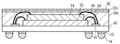
図4は実施例1に係る半導体装置の断面図である。図4を参照に、図1に対し、半導体チップ24の配線基板10とは反対の側にシート状樹脂部32aと、シート状樹脂部32aと配線基板10との間に設けられ半導体チップ22および24を封止する樹脂封止部30aとを有している。このとき、シート状樹脂部32aの厚さは約50μm、シート状樹脂部32aと半導体チップ24との間の樹脂封止部30aの厚さは約50μmである。また、ワイヤ28はシート状樹脂部32aに接している。その他の構成は図1と同じであり、同じ構成は同じ符号を付し説明を省略する。なお、シート状樹脂部32aの膜厚は10〜100μmとすることが好ましい。 FIG. 4 is a cross-sectional view of the semiconductor device according to the first embodiment. Referring to FIG. 4, with respect to FIG. 1, the sheet-shaped
実施例1によれば、図2(b)のように、半導体チップ24の配線基板10とは反対の側にシート状樹脂33aを配置し、シート状樹脂部32aを形成する。図3(b)のように、シート状樹脂33aと配線基板10との間に半導体チップ22および24を封止する樹脂封止部30aを形成する。このように、シート状樹脂33aが半導体チップ24の表面に配置された状態で樹脂封止部30aが形成される。よって、半導体チップ24の表面に樹脂部の未充填部が形成されることを抑制することができる。 According to the first embodiment, as shown in FIG. 2B, the sheet-shaped
また、図2(b)のように、下金型44の半導体チップ24が向かい合う面にシート状樹脂33aを配置することにより、半導体チップ24の表面にシート状樹脂部32aを形成することができる。 Further, as shown in FIG. 2B, the sheet-shaped
さらに、図3(a)のように、シート状樹脂33aと半導体チップ24との間に樹脂封止するための未硬化樹脂31を配置し、未硬化樹脂31で半導体チップ24を樹脂封止している。これにより、図4のように、シート状樹脂部32aと半導体チップ24との間に樹脂封止部30aの一部を設けることができる。よって、樹脂部に未充填部が形成されることを抑制することができる。 Further, as shown in FIG. 3A, an
さらに、図2(b)において配置したシート状樹脂33aはフィラーが不添加の樹脂である。よって、図4のシート状樹脂部32aはフィラーが不添加の樹脂となる。これにより、図1(a)で説明したようなフィラーの脱落部の発生を抑制することができる。さらに、樹脂封止部30aにはフィラーを添加することにより、樹脂部の強度を保つことができる。 Furthermore, the sheet-
さらに、図3(b)において、シート状樹脂33aの粘度を高くすることにより、成型中にワイヤ28がシート状樹脂33aに埋め込まれることを防止できる。よって、ワイヤ28はシート状樹脂部32aに接して形成される。これにより、ワイヤ28は樹脂部から露出することを抑制することができる。 Further, in FIG. 3B, by increasing the viscosity of the sheet-
実施例2はチップ搭載部として配線基板10を用い、樹脂封止部30bをトランンスファーモールド方式で成型した例である。図5(a)から図6(b)を用い、実施例2係る半導体装置の製造方法について説明する。図5(a)を参照に、半導体チップ22および24を樹脂封止するための上金型54と下金型50とを配置する。下金型50には被封止基板20を配置するための凹部57が設けられ、上金型54には樹脂封止部30bを成型するための空隙56が形成されている。さらに、下金型50に樹脂の格納部59、上金型54に樹脂を空隙56に導く注入路58が設けられている。 Example 2 is an example in which the
図5(b)を参照に、凹部57に被封止基板20を配置する。被封止基板20の構成は実施例1と同じであり、同じ構成には同じ符号を付し説明を省略する。上金型54の空隙56を上面に厚さ約100μmのシート状樹脂33bを配置する。つまり、配線基板10に搭載された半導体チップ24の配線基板10とは反対の側にシート状樹脂33bを配置する。言い換えれば、半導体チップ22および24を樹脂封止するための上金型54の半導体チップ24が向かい合う面53にシート状樹脂33bを配置する。シート状樹脂33bは、フィラーを有さず熱硬化性のエポキシ樹脂であり未硬化の状態で配置される。下金型50の格納部59に未硬化樹脂60を配置する。未硬化樹脂は、実施例1と同様に、フィラーを添加した熱硬化型のエポキシ樹脂である。 With reference to FIG. 5B, the substrate to be sealed 20 is disposed in the
図6(a)を参照に、上金型54と下金型50を合わせる。例えば175度に加熱する。このとき、シート状樹脂33aは実施例1のシート状樹脂33aに比べ粘度が低く、シート状樹脂33bにワイヤ28の少なくとも一部が埋め込まれる。また、シート状樹脂33bは半導体チップ24に接するように配置される。図6(b)を参照に、格納部59に挿入部62を導入することにより、未硬化樹脂60が注入路58を通りシート状樹脂33bと被封止基板20との間に注入される。以上により、未硬化のシート状樹脂33bが硬化しシート状樹脂部32bが形成される。また、配線基板10とシート状樹脂33bとの間に未硬化樹脂60が注入され半導体チップ22および24が封止され樹脂封止部30bが成型される。つまり未硬化樹脂60で半導体チップ22および24が樹脂封止される。なお、上金型54および下金型50を逆に配置し、被封止基板20を下の金型に、シート状樹脂33bを上の金型に配置してもよい。その後、被封止基板20を金型50、54から外し、配線基板10の半導体チップ22および24が搭載された面とは反対の面に半田ボール14を形成する。 Referring to FIG. 6A, the
図7は実施例2に係る半導体装置の断面図である。図7を参照に、図4に対し、ワイヤ28はシート状樹脂部32bに埋め込まれており、シート状樹脂部32bは半導体チップ24に接するように設けられている。その他の構成は図4と同じであり、同じ構成は同じ符号を付し説明を省略する。なお、実施例2ではシート状樹脂部32bの膜厚は約100μmである。この膜厚は、10〜150μmの範囲とすることが好ましい。 FIG. 7 is a cross-sectional view of the semiconductor device according to the second embodiment. Referring to FIG. 7, with respect to FIG. 4, the
トランスファーモールド法を用い封止樹脂する場合は、パッケージを薄くしようとすると、未硬化樹脂60を半導体チップ24と上金型54の間に注入することが求められる。このため樹脂の未充填部が発生しやすい。そこで、図6(a)および図6(b)のように、シート状樹脂33bが半導体チップ24に接するように半導体チップ22、24を樹脂封止する。つまり、シート状樹脂部32bは半導体チップ24に接するように設けられている。また、ワイヤ28の少なくとも一部はシート状樹脂部32bに埋め込まれている。これにより、トランスファーモールド法を用い封止樹脂する場合も半導体チップ24とシート状樹脂33bとの間に、樹脂部の未充填部が生じることを抑制することができる。 In the case of encapsulating resin using the transfer molding method, it is required to inject the
実施例1および実施例2のように、半導体チップ22および24は積層された半導体チップである。半導体チップを積層する場合、パッケージを薄くしようとすると、半導体チップ24上の樹脂部が薄くなり、特に、樹脂部に未充填部やフィラー脱落部、ワイヤの露出が発生しやすい。よって、本発明を適用することにより、よりその効果を奏することができる。 As in the first and second embodiments, the semiconductor chips 22 and 24 are stacked semiconductor chips. When the semiconductor chips are stacked, if the package is to be thinned, the resin portion on the
実施例3は図8のように樹脂封止部30cが、シート状樹脂部32cと半導体チップ24との間にも設けられ、ワイヤ28がシート状樹脂部32cに埋め込まれた例である。実施例1のようにバキュームデッピングモールド方式を用いた場合も、ワイヤ28をシート状樹脂部32cに埋め込ませることもできる。これにより、実施例1に比べ、パッケージを薄くすることができる。 In Example 3, as shown in FIG. 8, the
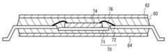
実施例4は、チップ搭載部としてリードフレーム70を用いた例である。図9を参照に、リードフレーム70はリード72と搭載部71を有している。搭載部71に半導体チップ74が搭載されている。半導体チップ74の搭載部71とは反対の側にシート状樹脂部82が設けられている。リード72の一部、搭載部71および半導体チップ74は樹脂封止部80により封止されている。シート状樹脂部82と搭載部71との間に樹脂封止部80が設けられ、半導体チップ74が樹脂封止されている。このように、リードフレーム70に半導体チップ74が実装された場合も、シート状樹脂部82を設けることができる。これにより、樹脂部に未充填部の発生またはワイヤの露出を抑制することができる。 Example 4 is an example in which a
リードフレーム70を用いたパッケージでは、図9のように樹脂封止部80がリードフレーム70の搭載部71の上下に設けられている。そこで、実施例5においては、図10のように、実施例4に加え、搭載部71の半導体チップ74とは反対の側に第2シート状樹脂部84が設けられ、樹脂封止部80は、シート状樹脂部82と第2シート状樹脂部84との間を封止する。これにより、搭載部71の半導体チップ74の側とは反対の側の樹脂封止部80を薄くした場合も、樹脂部の未充填部の発生を抑制することができる。実施例4および実施例5においては、シート状樹脂部82および第2シート状樹脂部84にフィラーを添加しないことによりフィラーの脱落部の発生を抑制することもできる。 In the package using the
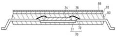
実施例6は、図11のように、実施例4の半導体装置に加え、シート状樹脂部82の半導体チップ74とは反対の側に導電性シート86が設けられている。また、図12のように、実施例3に係る半導体装置に加え、シート状樹脂部32cの半導体チップ24とは反対の側に導電性シート36が設けられている。導電性シート86および36は、例えば金属性シートや絶縁膜に配線を埋め込んだ構造とすることができる。例えば、ガラスエポキシ樹脂に銅配線を埋め込んだような構成とすることができる。導電性シート86および36を設けることにより、電磁波を遮蔽することができる。よって、電磁波障害等を抑制することができる。また、放熱板として機能する。さらに、パッケージの反りを抑制することもできる。さらに、レーザー捺印の際半導体チップ74および24にダメージが加わることを抑制することもできる。 In the sixth embodiment, as shown in FIG. 11, in addition to the semiconductor device of the fourth embodiment, a
シート状樹脂部32、82、84および樹脂封止部30、80は熱硬化性エポキシ樹脂以外も、例えば熱硬化性のポリイミド樹脂、マレイミド樹脂、シリコーン樹脂、フェノール樹脂、ポリウレタン樹脂またはアクリル樹脂を用いることができる。チップ搭載部は、絶縁基板に配線パターンを形成したパターンを設けた配線基板10や金属性材料よりなるリードフレーム70以外にも、半導体チップが搭載される部材であれば良い。シート状樹脂部32aから32cはフィラーを不添加の例であったが、フィラーを添加してもよい。 In addition to the thermosetting epoxy resin, for example, a thermosetting polyimide resin, a maleimide resin, a silicone resin, a phenol resin, a polyurethane resin, or an acrylic resin is used for the sheet-
以上、本発明の好ましい実施例について詳述したが、本発明は係る特定の実施例に限定されるものではなく、特許請求の範囲に記載された本発明の要旨の範囲内において、種々の変形・変更が可能である。
The preferred embodiments of the present invention have been described in detail above, but the present invention is not limited to such specific embodiments, and various modifications can be made within the scope of the gist of the present invention described in the claims.・ Change is possible.
Claims (13)
Translated fromJapanese前記半導体チップの前記チップ搭載部とは反対の側であって、かつ、前記半導体チップを樹脂封止するための金型の前記半導体チップが向かい合う面に、シート状樹脂を配置する工程と、
前記シート状樹脂と前記チップ搭載部との間において、未硬化樹脂を硬化させることにより、前記半導体チップを封止する樹脂封止部を形成する工程と、を有し、
前記チップ搭載部上において、前記半導体チップを前記樹脂封止部および前記シート状樹脂により封止する、半導体装置の製造方法。Mounting a semiconductor chip on the chip mounting portion;
Disposing a sheet-like resin on the opposite side of the chip mounting portion of the semiconductor chip and on the surface of the mold for resin-sealing the semiconductor chip facing the semiconductor chip;
Forming a resin sealing portion for sealing the semiconductor chip by curing an uncured resin between the sheet-shaped resin and the chip mounting portion;
A method of manufacturing a semiconductor device, wherein the semiconductor chip is sealed with the resin sealing portion and the sheet-like resin on the chip mounting portion.
該半導体チップを搭載するチップ搭載部と、
前記半導体チップの前記チップ搭載部とは反対の側に設けられたシート状樹脂部と、
前記シート状樹脂部と前記チップ搭載部との間に設けられ前記半導体チップを封止する樹脂封止部と、を具備し、
前記シート状樹脂部は前記半導体チップに接するように設けられており、
前記樹脂封止部はフィラーが添加された樹脂である一方、前記シート状樹脂部はフィラーが不添加の樹脂である、半導体装置。A semiconductor chip;
A chip mounting portion for mounting the semiconductor chip;
A sheet-like resin portion provided on the opposite side of the chip mounting portion of the semiconductor chip;
A resin sealing portion that is provided between the sheet-shaped resin portion and the chip mounting portion and seals the semiconductor chip;
The sheet-like resin portion is provided in contact with the semiconductor chip,
The resin sealing portion is a resin to which a filler is added, while the sheet-like resin portion is a resin to which a filler is not added .
該半導体チップを搭載するチップ搭載部と、
前記半導体チップの前記チップ搭載部とは反対の側に設けられたシート状樹脂部と、
前記シート状樹脂部と前記チップ搭載部との間に設けられ前記半導体チップを封止する樹脂封止部と、を具備し、
前記半導体チップと前記チップ搭載部とを接続するワイヤを具備し、前記ワイヤは前記シート状樹脂部に接しており、
前記樹脂封止部はフィラーが添加された樹脂である一方、前記シート状樹脂部はフィラーが不添加の樹脂である、半導体装置。A semiconductor chip;
A chip mounting portion for mounting the semiconductor chip;
A sheet-like resin portion provided on the opposite side of the chip mounting portion of the semiconductor chip;
A resin sealing portion that is provided between the sheet-shaped resin portion and the chip mounting portion and seals the semiconductor chip;
Comprising a wire connecting the semiconductor chip and the chip mounting portion, the wire is in contact with the sheet-like resin portion;
The resin sealing portion is a resin to which a filler is added, while the sheet-like resin portion is a resin to which a filler is not added .
該半導体チップを搭載するチップ搭載部と、
前記半導体チップの前記チップ搭載部とは反対の側に設けられたシート状樹脂部と、
前記シート状樹脂部と前記チップ搭載部との間に設けられ前記半導体チップを封止する樹脂封止部と、を具備し、
前記半導体チップと前記チップ搭載部とを接続するワイヤを具備し、前記ワイヤの少なくとも一部は前記シート状樹脂部に埋め込まれており、
前記樹脂封止部はフィラーが添加された樹脂である一方、前記シート状樹脂部はフィラーが不添加の樹脂である、半導体装置。A semiconductor chip;
A chip mounting portion for mounting the semiconductor chip;
A sheet-like resin portion provided on the opposite side of the chip mounting portion of the semiconductor chip;
A resin sealing portion that is provided between the sheet-shaped resin portion and the chip mounting portion and seals the semiconductor chip;
Comprising a wire connecting the semiconductor chip and the chip mounting portion, at least a part of the wire is embedded in the sheet-like resin portion;
The resin sealing portion is a resin to which a filler is added, while the sheet-like resin portion is a resin to which a filler is not added .
前記樹脂封止部は、前記シート状樹脂と前記第2シート状樹脂との間に設けられた、請求項8から10のいずれか一項に記載の半導体装置。Comprising a second sheet-like resin portion provided on the opposite side of the chip mounting portion from the semiconductor chip;
The resin sealing portion, said provided between the sheet-like resin and said second sheet-like resin, the semiconductor device according to any one of claims 810.
Applications Claiming Priority (1)
| Application Number | Priority Date | Filing Date | Title |
|---|---|---|---|
| PCT/JP2006/300543WO2007083352A1 (en) | 2006-01-17 | 2006-01-17 | Semiconductor device and method for manufacturing same |
Publications (2)
| Publication Number | Publication Date |
|---|---|
| JPWO2007083352A1 JPWO2007083352A1 (en) | 2009-06-11 |
| JP5036563B2true JP5036563B2 (en) | 2012-09-26 |
Family
ID=38287314
Family Applications (1)
| Application Number | Title | Priority Date | Filing Date |
|---|---|---|---|
| JP2007554753AExpired - Fee RelatedJP5036563B2 (en) | 2006-01-17 | 2006-01-17 | Semiconductor device and manufacturing method thereof |
Country Status (4)
| Country | Link |
|---|---|
| US (5) | US7566978B2 (en) |
| JP (1) | JP5036563B2 (en) |
| TW (1) | TWI344183B (en) |
| WO (1) | WO2007083352A1 (en) |
Cited By (1)
| Publication number | Priority date | Publication date | Assignee | Title |
|---|---|---|---|---|
| JP2012166432A (en)* | 2011-02-14 | 2012-09-06 | Apic Yamada Corp | Resin molding method, and resin molding apparatus |
Families Citing this family (23)
| Publication number | Priority date | Publication date | Assignee | Title |
|---|---|---|---|---|
| JP5036563B2 (en) | 2006-01-17 | 2012-09-26 | スパンション エルエルシー | Semiconductor device and manufacturing method thereof |
| KR20090043898A (en)* | 2007-10-30 | 2009-05-07 | 삼성전자주식회사 | Stacked packages and methods of manufacturing the same, and cards and systems comprising the stacked packages |
| US7923846B2 (en)* | 2007-11-16 | 2011-04-12 | Stats Chippac Ltd. | Integrated circuit package-in-package system with wire-in-film encapsulant |
| JP5543086B2 (en)* | 2008-06-25 | 2014-07-09 | ピーエスフォー ルクスコ エスエイアールエル | Semiconductor device and manufacturing method thereof |
| JP5086945B2 (en)* | 2008-09-05 | 2012-11-28 | 株式会社東芝 | Manufacturing method of semiconductor device |
| JP5715747B2 (en)* | 2008-09-30 | 2015-05-13 | セミコンダクター・コンポーネンツ・インダストリーズ・リミテッド・ライアビリティ・カンパニー | Circuit device and manufacturing method thereof |
| DE102009001373A1 (en)* | 2009-03-06 | 2010-09-09 | Robert Bosch Gmbh | Method for embedding an electrical assembly |
| CN102484102A (en)* | 2009-08-24 | 2012-05-30 | 本田技研工业株式会社 | Electronic device and method for manufacturing electronic device |
| JP2011054806A (en)* | 2009-09-02 | 2011-03-17 | Renesas Electronics Corp | Semiconductor device and method of manufacturing the same |
| JP5174874B2 (en)* | 2010-09-16 | 2013-04-03 | Towa株式会社 | Compression molding die and compression molding method |
| JP5824765B2 (en)* | 2011-01-11 | 2015-12-02 | アピックヤマダ株式会社 | Resin molding method, resin molding apparatus, and supply handler |
| CN104102422B (en)* | 2013-04-03 | 2018-05-01 | 阿里巴巴集团控股有限公司 | The page returns to the method and device of operation |
| CN105097748B (en)* | 2014-04-23 | 2018-07-13 | 北京富纳特创新科技有限公司 | Bonding line and semiconductor package part |
| JPWO2016092692A1 (en)* | 2014-12-12 | 2017-04-27 | 株式会社メイコー | Molded circuit module and manufacturing method thereof |
| JPWO2016092694A1 (en)* | 2014-12-12 | 2017-04-27 | 株式会社メイコー | Molded circuit module and manufacturing method thereof |
| WO2016092693A1 (en)* | 2014-12-12 | 2016-06-16 | 株式会社メイコー | Moudled circuit module, and production method therefor |
| WO2016092691A1 (en)* | 2014-12-12 | 2016-06-16 | 株式会社メイコー | Moulded circuit module, and production method therefor |
| WO2016092695A1 (en)* | 2014-12-12 | 2016-06-16 | 株式会社メイコー | Moulded circuit module, and production method therefor |
| JP6563593B2 (en)* | 2015-11-16 | 2019-08-21 | ヒューレット−パッカード デベロップメント カンパニー エル.ピー.Hewlett‐Packard Development Company, L.P. | Circuit package |
| FR3048305A1 (en)* | 2016-02-26 | 2017-09-01 | Stmicroelectronics (Grenoble 2) Sas | LOCALLY ENCAPSULATING BLOCK ELECTRONIC DEVICE WITH REDUCED THICKNESS |
| KR102420589B1 (en) | 2017-12-04 | 2022-07-13 | 삼성전자주식회사 | Semiconductor packages having a heat sink |
| US10304788B1 (en)* | 2018-04-11 | 2019-05-28 | Semiconductor Components Industries, Llc | Semiconductor power module to protect against short circuit event |
| US11031353B2 (en)* | 2019-08-23 | 2021-06-08 | Micron Technology, Inc. | Warpage control in microelectronic packages, and related assemblies and methods |
Family Cites Families (24)
| Publication number | Priority date | Publication date | Assignee | Title |
|---|---|---|---|---|
| SE9603787L (en)* | 1996-10-14 | 1998-04-15 | Combitech Traffic Syst Ab | Key device for control units in vehicles |
| US7469381B2 (en)* | 2007-01-07 | 2008-12-23 | Apple Inc. | List scrolling and document translation, scaling, and rotation on a touch-screen display |
| US20030205815A1 (en)* | 1999-06-09 | 2003-11-06 | Henry Chung | Fabrication method of integrated circuits with borderless vias and low dielectric constant inter-metal dielectrics |
| JP4150471B2 (en)* | 1999-06-24 | 2008-09-17 | 日東電工株式会社 | Manufacturing method of semiconductor element sealing sheet |
| US7830666B2 (en)* | 2000-01-06 | 2010-11-09 | Super Talent Electronics, Inc. | Manufacturing process for single-chip MMC/SD flash memory device with molded asymmetric circuit board |
| US6531407B1 (en)* | 2000-08-31 | 2003-03-11 | Micron Technology, Inc. | Method, structure and process flow to reduce line-line capacitance with low-K material |
| JP3420748B2 (en)* | 2000-12-14 | 2003-06-30 | 松下電器産業株式会社 | Semiconductor device and manufacturing method thereof |
| JP2003080537A (en)* | 2001-09-14 | 2003-03-19 | Citizen Electronics Co Ltd | Mold for molding plastics and molding method |
| US7312785B2 (en)* | 2001-10-22 | 2007-12-25 | Apple Inc. | Method and apparatus for accelerated scrolling |
| JP3739699B2 (en)* | 2001-12-20 | 2006-01-25 | 松下電器産業株式会社 | Method and apparatus for manufacturing electronic component mounted component |
| JP2003249607A (en)* | 2002-02-26 | 2003-09-05 | Seiko Epson Corp | Semiconductor device and its manufacturing method, circuit board, and electronic equipment |
| US7051169B2 (en)* | 2002-02-26 | 2006-05-23 | Kyocera Wireless Corp. | Memory configuration for a wireless communications device |
| JP2003258162A (en)* | 2002-02-27 | 2003-09-12 | Toshiba Corp | Primary and secondary mounting |
| JP2004031510A (en)* | 2002-06-24 | 2004-01-29 | Towa Corp | Resin member |
| JP4662324B2 (en)* | 2002-11-18 | 2011-03-30 | 太陽誘電株式会社 | Circuit module |
| JP4051326B2 (en)* | 2003-08-26 | 2008-02-20 | 京セラ株式会社 | Manufacturing method of electronic device |
| JP2005101356A (en)* | 2003-09-25 | 2005-04-14 | Toshiba Corp | Wireless card |
| JP4479209B2 (en)* | 2003-10-10 | 2010-06-09 | パナソニック株式会社 | Electronic circuit device, method for manufacturing the same, and apparatus for manufacturing electronic circuit device |
| JP2005157736A (en)* | 2003-11-26 | 2005-06-16 | Sony Corp | Radio communication module and method for manufacturing radio communication module |
| JP4089636B2 (en)* | 2004-02-19 | 2008-05-28 | 三菱電機株式会社 | Method for manufacturing thermally conductive resin sheet and method for manufacturing power module |
| JP2005242723A (en)* | 2004-02-27 | 2005-09-08 | Konica Minolta Photo Imaging Inc | Ic card |
| JP4553813B2 (en)* | 2005-08-29 | 2010-09-29 | Okiセミコンダクタ株式会社 | Manufacturing method of semiconductor device |
| JP5036563B2 (en)* | 2006-01-17 | 2012-09-26 | スパンション エルエルシー | Semiconductor device and manufacturing method thereof |
| JP4757056B2 (en)* | 2006-02-21 | 2011-08-24 | 富士通株式会社 | Resin layer forming method, semiconductor device and manufacturing method thereof |
- 2006
- 2006-01-17JPJP2007554753Apatent/JP5036563B2/ennot_activeExpired - Fee Related
- 2006-01-17WOPCT/JP2006/300543patent/WO2007083352A1/enactiveApplication Filing
- 2007
- 2007-01-17USUS11/654,703patent/US7566978B2/ennot_activeExpired - Fee Related
- 2007-01-17TWTW096101700Apatent/TWI344183B/ennot_activeIP Right Cessation
- 2009
- 2009-03-13USUS12/404,146patent/US8772953B2/ennot_activeExpired - Fee Related
- 2009-06-24USUS12/491,092patent/US7834470B2/ennot_activeExpired - Fee Related
- 2010
- 2010-10-07USUS12/900,370patent/US8530282B2/ennot_activeExpired - Fee Related
- 2013
- 2013-08-16USUS13/969,207patent/US8900928B2/enactiveActive
Cited By (1)
| Publication number | Priority date | Publication date | Assignee | Title |
|---|---|---|---|---|
| JP2012166432A (en)* | 2011-02-14 | 2012-09-06 | Apic Yamada Corp | Resin molding method, and resin molding apparatus |
Also Published As
| Publication number | Publication date |
|---|---|
| TWI344183B (en) | 2011-06-21 |
| US20080169552A1 (en) | 2008-07-17 |
| US7566978B2 (en) | 2009-07-28 |
| US20090256250A1 (en) | 2009-10-15 |
| US20110024922A1 (en) | 2011-02-03 |
| US8900928B2 (en) | 2014-12-02 |
| US20140035170A1 (en) | 2014-02-06 |
| US8772953B2 (en) | 2014-07-08 |
| US7834470B2 (en) | 2010-11-16 |
| US8530282B2 (en) | 2013-09-10 |
| WO2007083352A1 (en) | 2007-07-26 |
| TW200802638A (en) | 2008-01-01 |
| JPWO2007083352A1 (en) | 2009-06-11 |
| US20090174057A1 (en) | 2009-07-09 |
Similar Documents
| Publication | Publication Date | Title |
|---|---|---|
| JP5036563B2 (en) | Semiconductor device and manufacturing method thereof | |
| CN113130434B (en) | Package structure and manufacturing method thereof | |
| CN110875259B (en) | Semiconductor device with a semiconductor device having a plurality of semiconductor chips | |
| JP5192825B2 (en) | Semiconductor device, manufacturing method thereof, and manufacturing method of laminated semiconductor device | |
| US8890628B2 (en) | Ultra slim RF package for ultrabooks and smart phones | |
| US20140124906A1 (en) | Semiconductor package and method of manufacturing the same | |
| US20140124907A1 (en) | Semiconductor packages | |
| US10217685B2 (en) | Air-cavity package with dual signal-transition sides | |
| US11404348B2 (en) | Semiconductor package carrier board, method for fabricating the same, and electronic package having the same | |
| JP2007318076A (en) | Sip module | |
| JP2015176906A (en) | Semiconductor device and manufacturing method of semiconductor device | |
| JP6370920B2 (en) | Integrated circuit assembly having molding compound | |
| KR102561718B1 (en) | Integrated circuit packaging system with interposer support structure mechanism and method of manufacture thereof | |
| CN107546184B (en) | Semiconductor package and method for manufacturing the same | |
| US8546950B2 (en) | Semiconductor package and manufacturing method thereof | |
| US9123629B2 (en) | Chip package and method for forming the same | |
| US10629507B1 (en) | System in package (SIP) | |
| CN101286502A (en) | Semiconductor Package Structure | |
| US20060076694A1 (en) | Semiconductor device package with concavity-containing encapsulation body to prevent device delamination and increase thermal-transferring efficiency | |
| KR102603421B1 (en) | Integrated circuit packaging structure and manufacturing method thereof | |
| US11417581B2 (en) | Package structure | |
| CN112712153B (en) | Memory card structure and manufacturing method thereof | |
| US9318354B2 (en) | Semiconductor package and fabrication method thereof | |
| CN104218006A (en) | Semiconductor package | |
| JP4174008B2 (en) | Semiconductor device |
Legal Events
| Date | Code | Title | Description |
|---|---|---|---|
| RD04 | Notification of resignation of power of attorney | Free format text:JAPANESE INTERMEDIATE CODE: A7424 Effective date:20100303 | |
| RD03 | Notification of appointment of power of attorney | Free format text:JAPANESE INTERMEDIATE CODE: A7423 Effective date:20100616 | |
| RD03 | Notification of appointment of power of attorney | Free format text:JAPANESE INTERMEDIATE CODE: A7423 Effective date:20100805 | |
| A711 | Notification of change in applicant | Free format text:JAPANESE INTERMEDIATE CODE: A711 Effective date:20100922 | |
| A131 | Notification of reasons for refusal | Free format text:JAPANESE INTERMEDIATE CODE: A131 Effective date:20111129 | |
| A521 | Request for written amendment filed | Free format text:JAPANESE INTERMEDIATE CODE: A523 Effective date:20120105 | |
| A131 | Notification of reasons for refusal | Free format text:JAPANESE INTERMEDIATE CODE: A131 Effective date:20120403 | |
| A521 | Request for written amendment filed | Free format text:JAPANESE INTERMEDIATE CODE: A523 Effective date:20120510 | |
| TRDD | Decision of grant or rejection written | ||
| A01 | Written decision to grant a patent or to grant a registration (utility model) | Free format text:JAPANESE INTERMEDIATE CODE: A01 Effective date:20120605 | |
| A01 | Written decision to grant a patent or to grant a registration (utility model) | Free format text:JAPANESE INTERMEDIATE CODE: A01 | |
| A61 | First payment of annual fees (during grant procedure) | Free format text:JAPANESE INTERMEDIATE CODE: A61 Effective date:20120703 | |
| FPAY | Renewal fee payment (event date is renewal date of database) | Free format text:PAYMENT UNTIL: 20150713 Year of fee payment:3 | |
| R150 | Certificate of patent or registration of utility model | Ref document number:5036563 Country of ref document:JP Free format text:JAPANESE INTERMEDIATE CODE: R150 Free format text:JAPANESE INTERMEDIATE CODE: R150 | |
| FPAY | Renewal fee payment (event date is renewal date of database) | Free format text:PAYMENT UNTIL: 20150713 Year of fee payment:3 | |
| RD02 | Notification of acceptance of power of attorney | Free format text:JAPANESE INTERMEDIATE CODE: R3D02 | |
| FPAY | Renewal fee payment (event date is renewal date of database) | Free format text:PAYMENT UNTIL: 20150713 Year of fee payment:3 | |
| R250 | Receipt of annual fees | Free format text:JAPANESE INTERMEDIATE CODE: R250 | |
| S111 | Request for change of ownership or part of ownership | Free format text:JAPANESE INTERMEDIATE CODE: R313111 | |
| R350 | Written notification of registration of transfer | Free format text:JAPANESE INTERMEDIATE CODE: R350 | |
| R250 | Receipt of annual fees | Free format text:JAPANESE INTERMEDIATE CODE: R250 | |
| R250 | Receipt of annual fees | Free format text:JAPANESE INTERMEDIATE CODE: R250 | |
| R250 | Receipt of annual fees | Free format text:JAPANESE INTERMEDIATE CODE: R250 | |
| R250 | Receipt of annual fees | Free format text:JAPANESE INTERMEDIATE CODE: R250 | |
| LAPS | Cancellation because of no payment of annual fees |