JP5029893B2 - Light bulb shaped LED lamp and lighting device - Google Patents
Light bulb shaped LED lamp and lighting deviceDownload PDFInfo
- Publication number
- JP5029893B2 JP5029893B2JP2007223635AJP2007223635AJP5029893B2JP 5029893 B2JP5029893 B2JP 5029893B2JP 2007223635 AJP2007223635 AJP 2007223635AJP 2007223635 AJP2007223635 AJP 2007223635AJP 5029893 B2JP5029893 B2JP 5029893B2
- Authority
- JP
- Japan
- Prior art keywords
- led
- substrate
- holder
- light
- light source
- Prior art date
- Legal status (The legal status is an assumption and is not a legal conclusion. Google has not performed a legal analysis and makes no representation as to the accuracy of the status listed.)
- Expired - Fee Related
Links
Images


Classifications
- F—MECHANICAL ENGINEERING; LIGHTING; HEATING; WEAPONS; BLASTING
- F21—LIGHTING
- F21V—FUNCTIONAL FEATURES OR DETAILS OF LIGHTING DEVICES OR SYSTEMS THEREOF; STRUCTURAL COMBINATIONS OF LIGHTING DEVICES WITH OTHER ARTICLES, NOT OTHERWISE PROVIDED FOR
- F21V3/00—Globes; Bowls; Cover glasses
- F21V3/04—Globes; Bowls; Cover glasses characterised by materials, surface treatments or coatings
- F21V3/06—Globes; Bowls; Cover glasses characterised by materials, surface treatments or coatings characterised by the material
- F—MECHANICAL ENGINEERING; LIGHTING; HEATING; WEAPONS; BLASTING
- F21—LIGHTING
- F21K—NON-ELECTRIC LIGHT SOURCES USING LUMINESCENCE; LIGHT SOURCES USING ELECTROCHEMILUMINESCENCE; LIGHT SOURCES USING CHARGES OF COMBUSTIBLE MATERIAL; LIGHT SOURCES USING SEMICONDUCTOR DEVICES AS LIGHT-GENERATING ELEMENTS; LIGHT SOURCES NOT OTHERWISE PROVIDED FOR
- F21K9/00—Light sources using semiconductor devices as light-generating elements, e.g. using light-emitting diodes [LED] or lasers
- F21K9/20—Light sources comprising attachment means
- F21K9/23—Retrofit light sources for lighting devices with a single fitting for each light source, e.g. for substitution of incandescent lamps with bayonet or threaded fittings
- F—MECHANICAL ENGINEERING; LIGHTING; HEATING; WEAPONS; BLASTING
- F21—LIGHTING
- F21S—NON-PORTABLE LIGHTING DEVICES; SYSTEMS THEREOF; VEHICLE LIGHTING DEVICES SPECIALLY ADAPTED FOR VEHICLE EXTERIORS
- F21S8/00—Lighting devices intended for fixed installation
- F21S8/02—Lighting devices intended for fixed installation of recess-mounted type, e.g. downlighters
- F21S8/026—Lighting devices intended for fixed installation of recess-mounted type, e.g. downlighters intended to be recessed in a ceiling or like overhead structure, e.g. suspended ceiling
- F—MECHANICAL ENGINEERING; LIGHTING; HEATING; WEAPONS; BLASTING
- F21—LIGHTING
- F21V—FUNCTIONAL FEATURES OR DETAILS OF LIGHTING DEVICES OR SYSTEMS THEREOF; STRUCTURAL COMBINATIONS OF LIGHTING DEVICES WITH OTHER ARTICLES, NOT OTHERWISE PROVIDED FOR
- F21V3/00—Globes; Bowls; Cover glasses
- F—MECHANICAL ENGINEERING; LIGHTING; HEATING; WEAPONS; BLASTING
- F21—LIGHTING
- F21Y—INDEXING SCHEME ASSOCIATED WITH SUBCLASSES F21K, F21L, F21S and F21V, RELATING TO THE FORM OR THE KIND OF THE LIGHT SOURCES OR OF THE COLOUR OF THE LIGHT EMITTED
- F21Y2105/00—Planar light sources
- F21Y2105/10—Planar light sources comprising a two-dimensional array of point-like light-generating elements
- F—MECHANICAL ENGINEERING; LIGHTING; HEATING; WEAPONS; BLASTING
- F21—LIGHTING
- F21Y—INDEXING SCHEME ASSOCIATED WITH SUBCLASSES F21K, F21L, F21S and F21V, RELATING TO THE FORM OR THE KIND OF THE LIGHT SOURCES OR OF THE COLOUR OF THE LIGHT EMITTED
- F21Y2115/00—Light-generating elements of semiconductor light sources
- F21Y2115/10—Light-emitting diodes [LED]
- H—ELECTRICITY
- H01—ELECTRIC ELEMENTS
- H01L—SEMICONDUCTOR DEVICES NOT COVERED BY CLASS H10
- H01L2224/00—Indexing scheme for arrangements for connecting or disconnecting semiconductor or solid-state bodies and methods related thereto as covered by H01L24/00
- H01L2224/01—Means for bonding being attached to, or being formed on, the surface to be connected, e.g. chip-to-package, die-attach, "first-level" interconnects; Manufacturing methods related thereto
- H01L2224/42—Wire connectors; Manufacturing methods related thereto
- H01L2224/47—Structure, shape, material or disposition of the wire connectors after the connecting process
- H01L2224/48—Structure, shape, material or disposition of the wire connectors after the connecting process of an individual wire connector
- H01L2224/4805—Shape
- H01L2224/4809—Loop shape
- H01L2224/48091—Arched
- H—ELECTRICITY
- H01—ELECTRIC ELEMENTS
- H01L—SEMICONDUCTOR DEVICES NOT COVERED BY CLASS H10
- H01L2224/00—Indexing scheme for arrangements for connecting or disconnecting semiconductor or solid-state bodies and methods related thereto as covered by H01L24/00
- H01L2224/73—Means for bonding being of different types provided for in two or more of groups H01L2224/10, H01L2224/18, H01L2224/26, H01L2224/34, H01L2224/42, H01L2224/50, H01L2224/63, H01L2224/71
- H01L2224/732—Location after the connecting process
- H01L2224/73251—Location after the connecting process on different surfaces
- H01L2224/73265—Layer and wire connectors
Landscapes
- Engineering & Computer Science (AREA)
- General Engineering & Computer Science (AREA)
- Physics & Mathematics (AREA)
- Microelectronics & Electronic Packaging (AREA)
- Optics & Photonics (AREA)
- Led Device Packages (AREA)
- Arrangement Of Elements, Cooling, Sealing, Or The Like Of Lighting Devices (AREA)
- Non-Portable Lighting Devices Or Systems Thereof (AREA)
Description
Translated fromJapanese本発明は、LED(発光ダイオード)を光源として用いた電球形ランプおよびこのランプを用いた照明装置に関する。 The present invention relates to a light bulb shaped lamp using an LED (light emitting diode) as a light source and an illumination device using the lamp.
LEDは、その温度が上昇するに従い、光出力の低下とともに寿命も短くなることが知られている。このため、LEDを光源とするランプでは、LEDの温度上昇を抑制することが求められている。 It is known that the lifetime of an LED shortens as the light output decreases as its temperature rises. For this reason, in the lamp | ramp which uses LED as a light source, it is calculated | required to suppress the temperature rise of LED.
従来、こうした要請に配慮して、LEDから伝わる熱を外部に放出するための放熱部を備え、この放熱部を外部に露出させたLED電球が知られている(例えば、特許文献1参照。)。 Conventionally, in consideration of such a demand, an LED bulb that includes a heat radiating portion for releasing heat transmitted from the LED to the outside and exposes the heat radiating portion to the outside is known (for example, see Patent Document 1). .
この特許文献1の電球形LEDランプは、外部に露出する周部を有する金属製の外郭部材の光源取付け部に熱伝導するようにLEDが実装されたLED基板を取付けたものであり、LED基板の熱を金属製外郭部材の光源取付け部を介して周部に伝導させ、包熱効果を高めることによってLED基板の温度上昇を抑制している。
特許文献1の技術では、電球形LEDランプのLED基板と外郭部材の光源取付け部とが絶縁性部材を介して接続されていることから、熱伝導の抵抗が大きいので、光出力が大きく、発熱量の多い高出力用LED基板を用いた場合の放熱効果としては十分ではなかった。 In the technique of Patent Document 1, since the LED substrate of the bulb-type LED lamp and the light source mounting portion of the outer member are connected via an insulating member, the heat conduction resistance is large, so that the light output is large and heat is generated. When using a large amount of high-power LED substrate, the heat dissipation effect was not sufficient.
本発明は、上記課題に鑑みてなされたものであり、LED基板の温度上昇を効果的に抑制できる電球形LEDランプおよびこのLEDランプを用いた照明装置を提供することを目的とする。 The present invention has been made in view of the above problems, and an object of the present invention is to provide a light bulb shaped LED lamp that can effectively suppress an increase in temperature of an LED substrate and an illumination device using the LED lamp.
請求項1の電球形LEDランプは、外部に露出する周側面部、この周側面部の内側に一体に形成された光源取付け部を有する金属製のホルダと;このホルダの光源取付け部とは反対側に配設された口金と;金属基板、この金属基板の一面側に絶縁層を介して形成された配線パターン、前記金属基板の一面側に接着層を介して配設され、前記絶縁層の何れの表面よりも高い位置に配置されたLEDチップ、およびこのLEDチップと前記配線パターンとを接続するボンディングワイヤを有し、他面側が前記ホルダの光源取付け部に熱伝導するように取付けられたLED基板と;このLED基板を覆って前記ホルダの一面側に取付けられた透光性カバーと;前記LED基板の回路部品を有し、前記ホルダに設けられた点灯回路と;を具備していることを特徴とする。A light bulb shaped LED lamp according to claim 1 is a metal holder having a peripheral side surface portion exposed to the outside, a light source mounting portion integrally formed inside the peripheral side surface portion; and opposite to the light source mounting portion of the holder A base disposed on the side; a metal substrate, a wiring pattern formed on one side of the metal substrate via an insulating layer, and an adhesive layer on the one side of the metal substrate, It has an LED chip arranged at a position higher thanany surface, and a bonding wire for connecting the LED chip and the wiring pattern, and is attached so that the other surface side is thermally conducted to the light source mounting portion of the holder. An LED substrate; a translucent cover that covers the LED substrate and is attached to one side of the holder; and a lighting circuit that includes circuit components of the LED substrate and is provided in the holder. And wherein the door.
この発明で、ホルダは、鉄およびステンレス等の合金、またはこれらよりも熱伝導性が良い金属例えば銅およびその合金、更に、アルミニウムおよびその合金等を使用できる。この発明で、ホルダの放熱面積を増やすための構成として、ホルダの周側面部に、ローレット加工を施してその周側面部を粗面とすることは可能であり、これに代えて放熱フィンを形成することも可能である。更に、ホルダの周側面部を防錆のための保護膜でコーテングしてもよく、この場合、黒色の保護膜をコーテングすれば、ホルダから外部への熱輻射を更に向上できる点で好ましい。この発明で、ホルダに一体に形成された光源取付け部は、ネジ溝などからなるLED基板の取付け手段を有していてもよい。 In the present invention, the holder can use an alloy such as iron and stainless steel, or a metal having better thermal conductivity, such as copper and its alloy, and aluminum and its alloy. In this invention, as a configuration for increasing the heat radiation area of the holder, the peripheral side surface portion of the holder can be knurled to roughen the peripheral side surface portion, and instead, a heat radiation fin is formed. It is also possible to do. Further, the peripheral side surface portion of the holder may be coated with a protective film for preventing rust. In this case, it is preferable to coat a black protective film because the heat radiation from the holder to the outside can be further improved. In the present invention, the light source mounting portion formed integrally with the holder may have LED board mounting means formed of a screw groove or the like.
LED基板には、電気エネルギーを光に変換する発光素子、例えば半導体発光素子として発光ダイオード(LED)チップが実装されている。ただし、必要に応じてエレクトリックルミネッセンス素子(EL素子)をLEDチップに代えて用いることも可能である。
使用するLEDチップの数は複数個であって、基板に面実装されている。A light emitting diode (LED) chip is mounted on the LED substrate as a light emitting element that converts electrical energy into light, for example, a semiconductor light emitting element. However, if necessary, an electric luminescence element (EL element) can be used instead of the LED chip.
There are a plurality of LED chips to be used, and they are surface-mounted on the substrate.
LED基板の金属基板は、銅(Cu)やアルミニウム(Al)等の熱伝導性に優れた金属材料または合金材料によって一面側にLEDチップが面実装可能なように平板状に形成されている。金属基板の形状は矩形状、円形状、多角形状のいずれであってもよい。LED基板の他面側は、金属基板表面が直接または熱伝導性の良好な保護層を介して露出しており、ホルダの光源取付け部に直接または間接的に接触することによって熱伝導可能に取付けられている。 The metal substrate of the LED substrate is formed in a flat plate shape so that the LED chip can be surface-mounted on one side by a metal material or alloy material having excellent thermal conductivity such as copper (Cu) or aluminum (Al). The shape of the metal substrate may be any of a rectangular shape, a circular shape, and a polygonal shape. On the other side of the LED board, the surface of the metal board is exposed directly or through a protective layer with good thermal conductivity, so that it can be thermally conducted by directly or indirectly contacting the light source mounting part of the holder. It has been.
LED基板の金属基板の一面側には、絶縁性接着層を介してLEDチップが配設されており、LEDチップの配設箇所とは別の領域の基板の一面側に形成された絶縁層上には配線パターンが設けられている。このLEDチップと配線パターンとは、ボンディングワイヤによって接続されてLED基板の回路が形成されている。 An LED chip is disposed on one surface side of the metal substrate of the LED substrate via an insulating adhesive layer, and on the insulating layer formed on the one surface side of the substrate in a region different from the location where the LED chip is disposed Is provided with a wiring pattern. The LED chip and the wiring pattern are connected by a bonding wire to form an LED substrate circuit.
このLED基板の絶縁性接着層は、LEDチップを接着するダイボンド材等から構成されるものであって、LEDチップから基板への伝熱の抵抗部材となるが、その厚さ寸法が10〜100μmときわめて薄いものであるので、伝熱の抵抗は少ない。また、絶縁性接着層が比較的薄く構成されていても、個々のLEDチップ自体に印加される電圧および流れる電流はLED基板全体に比較して少なく、またLEDチップには絶縁性接着層側にサファイア等からなる絶縁性の素子基板が設けられているので、高度の絶縁性能は不要である。このように、比較的薄く構成された絶縁性接着層における熱抵抗は実質的に無視できる程度であり、LEDチップの発熱がきわめて良好に金属基板に放熱されることとなる。したがって、この金属基板の他面側をホルダの光源取付け部に直接または間接的に接触させることによって、熱伝導性能が飛躍的に向上し、光出力の高い高出力用LED基板を用いた場合であっても、十分な放熱効果と発揮することができる。 The insulating adhesive layer of the LED substrate is composed of a die bond material or the like that adheres the LED chip, and serves as a resistance member for heat transfer from the LED chip to the substrate, but the thickness dimension is 10 to 100 μm. Because it is extremely thin, there is little resistance to heat transfer. In addition, even if the insulating adhesive layer is configured to be relatively thin, the voltage applied to each LED chip itself and the flowing current are small compared to the entire LED substrate, and the LED chip has an insulating adhesive layer side. Since an insulating element substrate made of sapphire or the like is provided, a high degree of insulation performance is unnecessary. As described above, the thermal resistance of the insulating adhesive layer formed relatively thin is substantially negligible, and the heat generated by the LED chip is radiated to the metal substrate very well. Therefore, when the other surface side of this metal substrate is brought into direct or indirect contact with the light source mounting portion of the holder, the heat conduction performance is greatly improved, and a high output LED substrate with high light output is used. Even if it exists, it can exhibit with sufficient heat dissipation effect.
透光性カバーは、主に充電部をなすLED基板に対して他のものが接触することを妨げるため等に設けられるものであって、グローブ形状をなしていても、フラット状をなしていてもよい。このカバーがグローブである場合、その内面の一部に反射膜を設けることは妨げないとともに、カバーの形状は点状光源が発した光を例えば拡散または集光させるために任意形状とすることができる。更に、透光性カバーとして、点状光源が発した光を集光または拡散させるためのレンズを用いることも可能である。 The translucent cover is provided mainly to prevent other objects from coming into contact with the LED substrate that forms the charging part, and even if it has a glove shape, it has a flat shape. Also good. When this cover is a globe, it is not hindered to provide a reflective film on a part of its inner surface, and the shape of the cover may be any shape to diffuse or condense light emitted from a point light source, for example. it can. Furthermore, it is also possible to use a lens for condensing or diffusing the light emitted from the point light source as the translucent cover.
請求項1の発明では、金属基板に絶縁性接着層を介してLEDチップが実装されたLED基板の他面側をホルダの光源取付け部に直接または間接的に接触させることによって、光出力の高い高出力用LED基板を用いた場合であっても、十分な放熱効果と発揮することができる。 According to the first aspect of the present invention, the other surface side of the LED substrate on which the LED chip is mounted on the metal substrate via the insulating adhesive layer is brought into direct or indirect contact with the light source mounting portion of the holder, thereby increasing the light output. Even when a high-power LED substrate is used, a sufficient heat dissipation effect can be achieved.
請求項2は、請求項1記載の電球形LEDランプにおいて、配線パターン上に形成された光反射層を備え、LEDチップはこの光反射層より高い位置に配置されていることを特徴とする。さらに、ホルダの取付け部には前記LED基板の他面側が挿入される凹部を形成することができる。According to a second aspect of the present invention, in the bulb-type LED lamp according to the first aspect,a light reflecting layer formed on thewiring pattern is provided, and the LED chip is disposed at a position higher than the light reflecting layer. Furthermore, a concave portion into which the other surface side of the LED substrate is inserted can be formed in the attachment portion of the holder.
ホルダに形成された凹部は、LED基板の他面側が挿入可能な形状であればよく、深さ寸法は基板の厚さ寸法以下であればよい。このような凹部が形成されていると、LED基板の位置決めが容易であるとともに、光源取付け部とLED基板の他面側との間に粘性を有する充填物を介在させる場合に、充填物の流出を防止することができる。 The recessed part formed in the holder should just be the shape which can insert the other surface side of a LED board, and a depth dimension should just be below the thickness dimension of a board | substrate. When such a concave portion is formed, the LED substrate can be easily positioned, and when the viscous filler is interposed between the light source mounting portion and the other surface side of the LED substrate, the filling material flows out. Can be prevented.
請求項3は、請求項1または2記載の電球形LEDランプにおいて、前記ホルダの光源取付け部と前記LED基板の他面側との間には熱伝導性樹脂が設けられていることを特徴とする。 According to a third aspect of the present invention, in the light bulb shaped LED lamp according to the first or second aspect, a heat conductive resin is provided between the light source mounting portion of the holder and the other surface side of the LED substrate. To do.
ホルダの光源取付け部とLED基板の他面側との間に熱伝導性樹脂を設けることによって、これらの間に隙間が発生しにくくなり、熱伝導性が低下することが抑制される。 By providing the heat conductive resin between the light source mounting portion of the holder and the other surface side of the LED substrate, it becomes difficult to generate a gap between them, and the thermal conductivity is suppressed from decreasing.
請求項4は、請求項1ないし3いずれか一記載の電球形LEDランプにおいて、前記点灯回路は、前記回路部品が実装された回路基板を有しており、この回路基板が前記ホルダの他面側に配設され、前記LED基板および前記口金と電気的に接続されていることを特徴とする。 A light bulb shaped LED lamp according to any one of claims 1 to 3, wherein the lighting circuit includes a circuit board on which the circuit component is mounted, and the circuit board is provided on the other surface of the holder. It is arrange | positioned by the side and is electrically connected with the said LED board and the said nozzle | cap | die.
点灯回路はホルダの他面側に設けられるものであるが、ホルダの他面側に凹部を形成し、この凹部内に収容するのが好ましい。また、点灯回路の一部が口金の内側に収容される状態に配置されていてもよい。また、点灯回路とホルダとの間には絶縁部材を介在させておくのが好ましく、この絶縁部材には、合成樹脂例えばPP(ポリプロピレン)またはPBT(ポリブチレンテレフタレート)などを好適に用いることができる。 Although the lighting circuit is provided on the other surface side of the holder, it is preferable that a concave portion is formed on the other surface side of the holder and accommodated in the concave portion. Moreover, you may arrange | position in the state in which a part of lighting circuit is accommodated inside a nozzle | cap | die. Further, it is preferable to interpose an insulating member between the lighting circuit and the holder, and a synthetic resin such as PP (polypropylene) or PBT (polybutylene terephthalate) can be suitably used for the insulating member. .
請求項5は、請求項1ないし4いずれか一記載の電球形LEDランプにおいて、LED基板は、金属基板中央部のLEDチップの実装密度が疎であり、金属基板周縁部のLEDチップの実装密度が密となるように配置されていることを特徴とする。 The light bulb shaped LED lamp according to any one of claims 1 to 4, wherein the LED substrate has a low mounting density of the LED chip at the central portion of the metal substrate, and a mounting density of the LED chip at the peripheral portion of the metal substrate. Are arranged so as to be dense.
発熱部品であるLEDチップは、実装密度が高いほど互いに隣接する素子同士の熱影響が高くなり、点灯中の温度が上昇する傾向にある。ところが、LED基板は外部に露出する周側面部を一体に備えた金属製のホルダに取付けられるので、この周側面部に近い金属基板周縁部は放熱効果によって比較的温度が低くなることから、金属基板中央部と比較してLEDチップの実装密度を高めても温度上昇を抑制することが可能であることが分かった。 The LED chip that is a heat-generating component has a higher thermal effect between adjacent elements as the mounting density is higher, and the temperature during lighting tends to increase. However, since the LED substrate is attached to a metal holder that is integrally provided with a peripheral side surface exposed to the outside, the metal substrate peripheral portion near the peripheral side surface portion has a relatively low temperature due to the heat dissipation effect. It has been found that the temperature rise can be suppressed even if the mounting density of the LED chips is increased as compared with the central portion of the substrate.
請求項6は、請求項1ないし5いずれか一記載の電球形LEDランプにおいて、前記光源取付け部は、熱伝導性樹脂および接着樹脂を含んでなる接合材を介して周側面部の内側に一体に形成されていることを特徴とする。熱伝導性樹脂は例えば熱伝導率が比較的大きいシリコーン樹脂等であり、接着樹脂は相対的に接着性の良いシリコーン樹脂等である。熱伝導性シリコーン樹脂が光源取付け部とホルダの周側面部の内側を接着し、この熱伝導性シリコーン樹脂を接着性シリコーン樹脂が覆うような構造であってもよいし、逆に熱伝導性シリコーン樹脂が接着性シリコーン樹脂を覆っていても良い。 A light bulb shaped LED lamp according to any one of claims 1 to 5, wherein the light source mounting portion is integrated with the inside of the peripheral side surface portion via a bonding material including a heat conductive resin and an adhesive resin. It is characterized by being formed. The thermally conductive resin is, for example, a silicone resin having a relatively high thermal conductivity, and the adhesive resin is a silicone resin having relatively good adhesiveness. The structure may be such that the heat conductive silicone resin adheres to the inside of the peripheral side surface portion of the light source mounting portion and the holder, and this heat conductive silicone resin is covered with the adhesive silicone resin. The resin may cover the adhesive silicone resin.
いずれの場合であっても同種の接着材がよく、接着材の熱膨張係数の違いによる剥離を低減することができる。このような構成により、LEDチップから放射された熱は金属基板に伝熱し、熱伝導性樹脂に伝熱し、さらにホルダに伝熱して周側面部から外部に放射される。なお、熱伝導性シリコーン樹脂が接着性シリコーン樹脂を覆っている場合には、熱伝導性シリコーン樹脂表面から熱を放射することもできるので、放熱効果が向上する。 In any case, the same kind of adhesive is good, and peeling due to the difference in thermal expansion coefficient of the adhesive can be reduced. With such a configuration, the heat radiated from the LED chip is transferred to the metal substrate, transferred to the heat conductive resin, further transferred to the holder, and radiated to the outside from the peripheral side surface portion. In addition, since heat can also be radiated | emitted from the surface of a heat conductive silicone resin when the heat conductive silicone resin has covered the adhesive silicone resin, the heat dissipation effect improves.
請求項7の照明装置は、ソケットを有する器具本体と;この器具本体のソケットに装着される請求項1ないし6いずれか一記載の電球形LEDランプと;を具備していることを特徴とする。 The lighting device according to
本発明の電球形LEDランプによれば、金属基板に絶縁性接着層を介してLEDチップが実装されたLED基板の他面側をホルダの光源取付け部に直接または間接的に接触させることによって、光出力の高い高出力用LED基板を用いた場合であっても、十分な放熱効果と発揮することができ、高温状態での継続的な使用によってLEDチップの光出力性能が低下することを抑制することができる。 According to the light bulb shaped LED lamp of the present invention, by directly or indirectly contacting the light source mounting portion of the holder with the other surface side of the LED substrate on which the LED chip is mounted on the metal substrate via the insulating adhesive layer, Even when a high-power LED substrate with high light output is used, it can exhibit a sufficient heat dissipation effect and suppress the light output performance of the LED chip from being deteriorated by continuous use at high temperatures. can do.
図1〜図3を参照して本発明の第1実施形態を説明する。 A first embodiment of the present invention will be described with reference to FIGS.
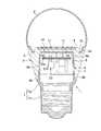
図1及び図2中符号1は電球形LEDランプ(以下ランプと略称する。)を示している。このランプ1は、金属製のホルダ2と、LEDチップ11と、透光性のカバー9と、点灯回路21と、絶縁部材6と、口金7とを具備している。 Reference numeral 1 in FIGS. 1 and 2 denotes a light bulb-type LED lamp (hereinafter abbreviated as a lamp). The lamp 1 includes a
ホルダ2は例えばアルミニウムの一体成形品からなる。図2及び図3に示すようにホルダ2は、外周面部3と、これと一体の光源取付け部4とからなり、外周面部3の内側に凹部5が形成されている。光源取付け部4は周部3の軸方向一端を閉じた奥壁で形成されており、凹部5は外周面部3の軸方向他端に開口されている。 The
外周面部3は、放熱面として機能するものであって、光源取付け部4から凹部5の開口縁部2aに向けて次第に径が小さくなる円錐状のテーパ面で形成されている。開口縁部2aの内周面には環状をなす係止溝2bが設けられている。外周面部3と光源取付け部4とが一体に連続する部位に環状の溝2cが形成されている。 The outer
溝2cは、例えば光源取付け部4を囲んで環状に設けられていて、光源取付け部4の周部外面に開放されている。この環状の溝2cはカバー取付け溝を兼ねている。また、光源取付け部4の中央部には凹部4aが設けられている。 For example, the
LED基板12には、LEDチップ11が100個実装されている。LEDチップ11の定格電流値は35mAであり、LED基板12の消費電力は13Wで、光出力は約800lmである。なお、本実施形態および他の実施形態の説明のために示す図面では、LEDチップ11の配置構造を分かりやすく説明するためにLEDチップ11を簡略化して記載しているので、LEDチップ11の大きさおよび実装数は実際のものとは相違している。 100
ホルダ2に形成された凹部4aは、LED基板12の他面側が挿入可能であり、深さ寸法は基板12の全体の厚さ寸法の約1/2である。この凹部4aによってLED基板12をホルダ2に固定する際に位置決めが容易に行うことができる。 The
また、凹部4aには、熱伝導性材料4bが充填されている。この熱伝導性材料4bは、グリース状のシリコーン樹脂に放熱用の金属酸化物等が混合されたものや、放熱用の金属酸化物を混合したエポキシ樹脂等の熱伝導性に優れた粘性を有する樹脂であり、光源取付け部とLED基板の他面側との間に隙間が発生することを防止して熱伝導性が低下することが抑制している。また、凹部4aに熱伝導性材料4bを充填することによって、粘性を有する熱伝導性材料4bが光源取付け部4以外の領域へ流出することを防止している。 The
LED基板12は、光源取付け部4の凹部4aに挿入された後、その基板周縁に図示しない接着剤を塗布することによってホルダ2に接着されている。なお、LED基板12のホルダ2への固着手段は接着剤に限定されることはなく、取付けねじやファスナ等の周知の取付け手段を用いることができる。 After the
透光性のカバー9は、ガラスまたは合成樹脂製などにより例えば半球状に形成されたグローブからなる。カバー9はその開口縁部9aをホルダ2の溝2cに嵌めることによってホルダ2に装着されている。したがって、カバー9は、光源取付け部4を覆い隠しており、LEDチップ11はカバー9の内面に対向している。 The translucent cover 9 is made of, for example, a globe formed in a hemispherical shape made of glass or synthetic resin. The cover 9 is attached to the
LEDチップ11を点灯させるための点灯回路20は、図2に示すように回路基板21aに各種の回路部品21bを取付けて、ユニット化されている。回路基板21aは円形状をなしており、回路部品21bはコンデンサ(図示しない)を含んでいる。回路部品21bの多くは、そのリード端子を回路基板21aに貫通させて回路基板21aの一面側に実装されていて、前記リード端子は回路基板21aの他面に設けられている図示しない回路パターンに半田付けされている。 The
点灯回路20は凹部5に収容されている。この点灯回路20はLEDチップ11に電気的に接続するための図示しない絶縁被覆電線と、後述する口金7に接続するための図示しない絶縁被覆電線とが導出されている。なお、点灯回路20は、その回路部品21bをLED基板12に実装することでLED基板12に一体的に実装して構成してもよい。 The
絶縁部材6は合成樹脂例えばポリブチレンテレフタレートの成形体である。この絶縁部材6は、後述する口金7に向けて開口するとともにこの開口側ほど大径となる円筒状部6b、及びこの円筒状部6bの一端に連続して前記開口に対向する閉鎖壁部6aを有してカップ状をなしている。絶縁部材6は、その外周面を凹部5の内周面に接触させるとともに、閉鎖壁部6aの外面を光源取付け部4の内面に接触させて設けられている。この絶縁部材6の内側に点灯回路20が収容されている。この場合、点灯回路20は、回路基板21aのリード端子が突出された面を閉鎖壁部6aに対向させるとともに、回路部品21bが実装された面を絶縁部材6の開口に向けた横置き姿勢で絶縁部材6に収容されている。 The insulating
点灯回路20に電源を供給するために外郭部材2の開口縁部2a側に配設された口金7は、口金要素7aこの口金要素7aに固定される連結部材7bとを有している。図示しないランプソケットに着脱自在に取付けられる口金要素7aは、その周部に例えば螺旋状のねじ山を有していて、図示しないランプソケットに着脱自在にねじ込まれる部分をなしている。連結部材7bは、合成樹脂例えばポリブチレンテレフタレートなどの絶縁材製であり、凹部5の開口縁部2aに接続されている。 A
このランプ1は、ホルダ2に設けた凹部5に点灯回路21を収容したので、点灯回路20を配置するためのスペースを外郭部材2に対してその軸方向に並べて確保する必要がない。これにより、ランプ1の軸方向長さが短くなり、コンパクトなランプ1とすることができる。 Since the lamp 1 accommodates the lighting circuit 21 in the
図3は、LED基板12の要部を拡大して示す断面図、図4はその上面図である。LED基板12は、パッケージ基板例えば金属基板13と、銀メッキ層14、絶縁層15と、複数の導体28と、複数の半導体発光素子例えばLEDチップ11と、ボンディングワイヤ27と、封止部材22とを備えて形成されている。 FIG. 3 is an enlarged cross-sectional view showing a main part of the
金属基板12aは、銅(Cu)からなるとともに、LED基板12して必要とされる発光面積を得るために所定形状例えば円盤形状をなしている。金属基板12aの一面側には、この金属基板12aと一体の凸部からなる素子取付け部13が例えばLEDチップ11と同数形成されている。素子取付け部13を除いた基板12aの主部の厚みは例えば0.18mmである。金属基板12aは、ホルダ4の凹部4aに挿入され、粘性を有する熱伝導性材料4bを介して光源取付け部4に金属基板12aの他面12cが接触するように取付けられている。 The
素子取付け部13の先端面13aは一面12bと平行な平坦面をなしている。素子取付け部13はその先端面13aから金属基板12aの一面12bに至るに従い次第に太く形成されている。言い換えれば、素子取付け部13は、その高さ方向と直交する断面積が先端面13aから金属基板12aの一面12bに至るに従い次第に大きくなる円錐台状に形成されている。そのため、素子取付け部13はその先端面13aから金属基板12aの一面にわたるテーパ状周面13bを有している。このテーパ状周面13bと金属基板12aの一面12bとはこれらの間に角を作ることなく弧状をなして連続している。先端面13aの直径は例えば0.57mmであり、素子取付け部13の最大径をなす根元の直径は例えば1.08mmである。 The
表面素子取付け部13の略全体に銀メッキ層14が被着されている。この銀メッキ層14は、表面素子取付け部13の先端面13a全体に被着された端面メッキ部14aと、これに一体に連続した表面素子取付け部13のテーパ状周面13bの略全体に被着された周面数メッキ部14bとからなる。銀メッキ層14は無電解メッキにより設けられた薄膜であって、その膜厚は例えば0.3μm〜0.4μmである。この銀メッキ層14の光の反射率は90%以上である。 A
絶縁層15には光反射性能を得るために例えば白色のガラスエポキシ基板が用いられている。なお、本実施例では絶縁層15を一層としたが、これは二層とすることもでき、それにより、一層のものよりも高い絶縁耐圧を確保できる。絶縁層15は素子取付け部3が個々に挿入される複数の通孔16を有している。通孔16は例えば円形で、その直径は素子取付け部13の最大径をなす根元部の直径以上に大きい。本実施形態では素子取付け部13の根元部の直径と同径の1.08mmとしてある。 For example, a white glass epoxy substrate is used for the insulating
絶縁層15は金属基板2の一面2bに接着層17により貼り合わされ金属基板12aに積層されている。接着層17は、紙や布等の繊維材料からなるシートに熱硬化性の接着樹脂を含浸してなり、絶縁層15の通孔16に個別に連通する複数の孔を有している。これらの孔の円形の縁によって、貼り合わせに伴い通孔16に挿入された素子取付け部13に向けて食み出した食み出し部17aを形成することが好ましい。この食み出し部17aはテーパ状周面3bに被着された周面メッキ部14bに連続している。 The insulating
なお、絶縁層15が金属基板12aに接着される前の状態では、接着層17の孔の直径は通孔16の直径より多少大きいが、食み出し部17aは、絶縁層15が金属基板12aに接着されるに伴い形成される。これは、予め接着層17が貼り付けられた絶縁層15を金属基板12aに押付けた状態のままで加熱炉に通して接着層17を加熱硬化することに伴い、前記押付けにより接着層17が圧縮されて変形することで、接着層17の孔が通孔16の直径より縮径されるからである。通孔16の内面16aに対する食み出し部17aの食み出し寸法Aは0.2mm以下である。この食み出し寸法Aは、接着層17の厚み及び金属基板12aへの絶縁層15の押付け力の加減等により規定できる。 In the state before the insulating
複数の導体18は、各LEDチップ11への通電要素としてこれらLEDチップ11を直列に接続するために、絶縁層15の金属基板12aに接着された裏面とは反対側の面にエッチング処理等により形成されている。これらの導体18は、銅(Cu)からなり、絶縁層15を金属基板12aに貼り合わせる前に設けられる。各導体18は、絶縁層15の長手方向に所定間隔毎に点在して二列形成されている。各列での複数の導体18は所定ピッチで各通孔16と交互に並べられている。 In order to connect the LED chips 11 in series as current-carrying elements to the LED chips 11, the plurality of
各LEDチップ11は例えば青色の光を発する青色LEDチップ11からなる。このLEDチップ11は、例えば窒化物半導体を用いてなるダブルワイヤー型であって、透光性を有する素子基板22の一面に半導体発光層23を積層して形成されている。素子基板22は例えばサファイア基板で作られている。半導体発光層23は反射膜を有しておらず、LEDチップ11の厚み方向の双方に光を放射できるとともに、素子基板22の側面から側方へも光を放射できる。 Each
これらのLEDチップ11は、素子基板22の前記一面と平行な他面を接着剤例えば透光性のシリコーン樹脂からなるダイボンド材26を用いて各素子取付け部3の先端面13aを覆っている銀メッキ層14の端面メッキ部14a上にダイボンドされている。それによって、各LEDチップ11は各導体8と交互に配置されている。ダイボンド材26の厚みは0.10mm以下である。ダイボンド材26はLEDチップ11から素子取付け部13への伝熱の抵抗部材となるが、以上のようにきわめて薄いので、このダイボンド材26での熱抵抗は実質的に無視できる程度である。金属基板12aの長手方向に交互に配置された導体18とLEDチップ11とは、ワイヤボンディングにより設けられたボンディングワイヤ27で電気的に直列に接続されている。 In these
LEDチップ11の半導体発光層23と素子取付け部13との間の絶縁耐圧は、ダイボンド材26だけではなく、このダイボンド材26よりもはるかに厚いサファイア製の素子基板22で確保されている。半導体発光層23の高さ位置を導体18表面の光反射層10より高く位置させるために、本実施形態ではLEDチップ11全体が導体8表面の光反射層10より高く位置されている。なお、LED基板12には光反射層10、銀メッキ層14を設けなくてもよい。 The withstand voltage between the semiconductor
こうした高さの差によって、ワイヤボンディングにおいて、ボンディングマシンでボンディングワイヤ17の一端を半導体発光層23の電極24,25にボールボンディングにより接合した後に、このボンディングワイヤ27の他端を導体18に接合する際、ボンディングマシンのボンディングツールの移動に絶縁層15が邪魔になり難く、又、ボンディングワイヤ27を斜め下方に無理に引くこともないので、ワイヤボンディングがし易い。 Due to the difference in height, in wire bonding, one end of the
更に、本実施形態のようにLEDチップ11全体が絶縁層15の表面よりも高い位置に配置されている好ましい構成では、LEDチップ11からその周囲に放射される光が、絶縁層15に妨げられることなく、通孔16の周辺に差し込み易い。それにより、LEDチップ11のまわりで光を反射させて光を取出すことができるので、光の取出し効率を高めることができる点で有利である。 Further, in a preferred configuration in which the
なお、本発明は、一つの素子取付け部13に一個のLEDチップ11を取付けることに制約されることはなく、一つの素子取付け部13に複数個のLEDチップ11を並べて取付けることも可能である。その場合、同じ色の光を発する複数個のLEDチップ11であっても、或いは異なる色の光を発する複数個のLEDチップ11であってもよく、異なる色の光を発する複数個のLEDチップ11を一つの素子取付け部13に取付ける場合には、赤色、黄色、青色の光を発する3個のLEDチップ11を並べて取付けることもできる。そして、一つの素子取付け部13に複数個のLEDチップ11を並べて取付けた構成においては、LED基板12の全光束を向上させることが可能である。 The present invention is not limited to mounting one
以上のように銀メッキ層14が略全体に被着された素子取付け部13を有した金属基板12a、光反射層10を有した導体18付きの絶縁層5、LEDチップ11、ボンディングワイヤ27によって、LED基板12の面状発光源が形成されている。 As described above, the
封止部材22は、リフレクタ20内に未硬化の状態で注入された後硬化されたものであり、前記面状発光源を埋めている。この封止部材22は絶縁層5の通孔6内に充填されている。それにより、封止部材22は、銀メッキ層14で覆われた素子取付け部3のテーパ状周面13b及び食み出し部17aに通孔16内で接してこれらを覆っている。封止部材22は、熱硬化性の透光性材料例えば透明シリコーン樹脂からなり、その内部に蛍光体(図示しない)が混入されている。本実施形態では白色系の照明光を得るために、LEDチップ11が発する光(具体的に青色の光)の一部により励起されて、このLEDチップ11が発する光とは異なる色の光(具体的には黄色の光)を放射する蛍光体が用いられ、この蛍光体は好ましくは略均一に分散した状態で封止部材22内に混入されている。 The sealing
この組み合わせにより、LED基板12の点灯により半導体発光層23から放出された青色の光の一部が蛍光体に当たることなく封止部材22を通過する一方で、青色の光が当たった蛍光体が励起されて黄色の光を放射し、この黄色の光が封止部材22を通過するので、これら補色関係にある二色の光の混合によってLED基板12は白色光を照射できる。 By this combination, a part of blue light emitted from the semiconductor
LED基板12は、各LEDチップ11に通電して、これらLEDチップ11を発光させることにより図3中矢印方向に光を取出して照明を行う。この点灯時に各LEDチップ11は発熱するが、LEDチップ11用の導体18の絶縁層15は金属基板12aとLEDチップ11との間には介在されていないとともに、LEDチップ11は金属基板12aの素子取付け部13上に直接的にダイボンドされているので、各LEDチップ11が発する熱は、絶縁層15に邪魔されることなく金属基板12aに直接的に伝導する。より具体的には、LEDチップ11の熱は、実質的に熱抵抗とはならないほど薄いダイボンド材26を通ってから、銀メッキ層14を経て金属基板12aの素子取付け部13に伝えられる。しかも、素子取付け部13は、LEDチップ11がダイボンドされた先端面13aから金属基板12aの主部に至るに従い次第に太く、言い換えれば、素子取付け部13の断面積が基板12aの主部に近付く程大きくなっているので、LEDチップ11から基板12aの主部に向けての熱伝導がより容易となる。そして、金属基板12aの熱はこの金属基板12aの背面12cからホルダ2の光源取付け部4に伝熱され、ホルダ2の周側面部3から放熱されるので、LEDチップ11の温度上昇は抑えられる。 The
こうしてLEDチップ11の熱が高効率に金属基板12aを介してホルダ2から外部に放出されるので、各LEDチップ11の温度上昇が効果的に抑制され、各LEDチップ11の温度を設計通りに維持できる。そのため、各LEDチップ11の発光効率の低下と、各LEDチップ11が発する光量のばらつきが抑制され、その結果的として、電球形LEDランプ1内の各LEDチップ11の発光効率の低下と発光色のむらを抑制できる。 Thus, the heat of the
図5は、LEDチップ11の配置を説明するLED基板12の概略上面図である。図5に示すように、円盤状のLED基板12の一面側には、多数のLEDチップ11が面状に実装されているが、その実装密度はLED基板12の中央部のLEDチップ11aの実装密度が疎であり、金属基板12の周縁部に向かうに従いLEDチップ11bの実装密度が次第に密となるように配置されている。 FIG. 5 is a schematic top view of the
発熱部品であるLEDチップ11は、実装密度が高いほど互いに隣接する素子同士の熱影響が高くなり、点灯中の温度が上昇する傾向にある。ところが、LED基板12は外部に露出する周側面部3を一体に備えた金属製のホルダ2に取付けられるので、この周側面部3に近い金属基板12aの周縁部付近は放熱効果によって比較的温度が低くなる。このため、金属基板12aの中央部付近よりもLEDチップ11の実装密度を高めても温度上昇を抑制することが可能であることが分かった。 The
このように、金属基板12aの中央部のLEDチップ11aの実装密度を高くしてLEDチップ11a同士の実装間隔を大きくし、金属基板12aの周縁部付近のLEDチップ11bの実装間隔を小さくすることで、各LEDチップ11の放熱効果が良好となり、熱影響に伴うランプ効率の低下が抑制される。また、各LEDチップ11の熱影響が均一化されることで、LED基板12の輝度均斉度が向上して輝度むらの発生を抑えることができる。 As described above, the mounting density of the LED chips 11a at the center of the
図6は、第2の実施形態の電球形LEDランプに使用されるLED基板12のLEDチップ11の配置を説明するLED基板12の概略上面図である。本実施形態の金属基板12aは八角形状の基板12を有しており、この基板12の一面側に格子状に配列された多数のLEDチップ11が面状に実装されている。その実装密度は、図5の実施形態と同様にLED基板12の中央部のLEDチップ11aの実装密度が疎であり、金属基板12の周縁部に向かうに従いLEDチップ11bの実装密度が次第に密となるように配置されている。このような配置構造にすることで、図5のLED基板12と同様の作用効果を奏することができる。 FIG. 6 is a schematic top view of the
また、LED基板12の形状が八角形であるので、LEDチップ11が実装されていない周縁部のスペースに点灯回路20との電気接続端子を配置したり、取付け手段を配置することができる。 Moreover, since the shape of the
図7は、第3の実施形態の電球形LEDランプに使用されるLED基板12の要部を拡大して示す概略上面図である。 FIG. 7 is a schematic top view showing an enlarged main part of the
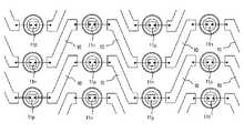
本実施形態のLED基板12は、交流電力で点灯するようにLEDチップ11が正極点灯用11pと負極点灯用11nの2種類の向きで点灯するように実装されており、正極点灯用11pおよび負極点灯用11nがそれぞれ直列回路を形成して、これら回路が最終的に並列接続されて一対の入力端子を形成し、この入力端子を介して点灯回路20から電力が入力されるよう回路を形成している。このような回路構成であれば、交流電力が入力されてもLEDチップ11が正極点灯用11pと負極点灯用11nの2種類の直列回路が交互に点灯するため、明るさのちらつきが発生することがなく、回路効率的にも有利である。 The
しかし、LEDチップ11の正極点灯用11pと負極点灯用11nの2種類がそれぞれ直線的な配列で実装された場合には、輝度むらが発生する可能性がある。本実施形態では、このような不具合を解消するために、見かけ上の直線位置に正極点灯用11pと負極点灯用11nの2種類のLEDチップ11が交互に配置されるように導電パターン10を形成している。この配置構成によって、片方の極性の回路に何らかの不具合が発生した場合であっても、点灯時の見え方としては全体として輝度が低下するものの、輝度むらはほとんど目立たないので、点灯外観が損なわれることがない。 However, when two types of
次に、本発明の第4実施形態を示す電球形LEDランプについて図8ないし9を参照して説明する。なお、第1実施形態と同じまたは同等の構成要素については、同一の符号を付してその詳細なる説明は省略する。 Next, a light bulb shaped LED lamp showing a fourth embodiment of the present invention will be described with reference to FIGS. In addition, about the component same or equivalent to 1st Embodiment, the same code | symbol is attached | subjected and the detailed description is abbreviate | omitted.
本実施形態の電球形LEDランプ1は、光源取付け部4が、熱伝導性樹脂30aおよび接着樹脂30bを含んでなる接合材30を介して周側面部3の内側に一体に形成されており、他の構成要素は第1実施形態のものとほぼ同様である。前記熱伝導性樹脂30aは熱伝導率が比較的大きいシリコーン樹脂であり、接着樹脂30bは相対的に接着性の良いシリコーン樹脂を使用している。熱伝導性シリコーン樹脂30aが光源取付け部4とホルダ2の周側面部3の内側を接着し、この熱伝導性シリコーン樹脂30aを接着性シリコーン樹脂30bが覆うような構造である。また、接着性シリコーン樹脂30bは透光性カバー9とホルダ2の境界部に配設されているので、透光性カバー9とホルダ2との接合を強固にすることもできる。 In the light bulb shaped LED lamp 1 of the present embodiment, the light
このような構成により、LEDチップ11から放射された熱は金属基板12aに伝熱し、熱伝導性樹脂30aに伝熱し、さらにホルダ2に伝熱して周側面部3から外部に放射され、ランプ内部が高温となることを低減している。このときに電球形LEDランプ1の温度を測定したグラフが図9である。図9のグラフの横軸はランプ点灯からの経過時間を1目盛10分で示し約60分の測定時間であり、縦軸は温度を示している。また、グラフ中、LEDチップ上温度(T1)は図8のT1の部分の温度を示し、金属基板下温度(T2)は図8のT2の部分の温度を示し、金属基板温度(T3)は図8のT3の部分の温度を示し、ホルダ温度(T4)は図8のT4の部分の温度を示し、周囲温度(T5)は図8のT5の部分の温度を示している。このグラフによると、LEDチップ、金属基板、ホルダの順に温度が低くなっているので、熱伝導性樹脂30aがLEDチップ11の熱を効果的に伝熱してホルダ2外に放熱されているもの考えられる。 With such a configuration, the heat radiated from the
次に、電球形LEDランプを光源とした照明器具の構成を説明する。図10に示すように、30は店舗等の天井面Xに設置された埋込み形ダウンライトとしての照明器具であり、下面に開口部31aを有する金属製の箱状をなした本体ケース31と、開口部31aに嵌合される金属製の反射体32で構成されている。反射体32は、例えばアルミニウム等の金属板で構成し、下面周囲に飾り枠32a一体に形成されている。反射体32の上面板の中央部には、電球形LEDランプ1の口金をねじ込むソケット33を配設する。 Next, the structure of the lighting fixture which used the light bulb-shaped LED lamp as a light source will be described. As shown in FIG. 10, 30 is a lighting fixture as an embedded downlight installed on a ceiling surface X of a store or the like, and a
この照明器具30は、光源となる電球形LEDランプ1の配光が一般白熱電球の配光に近似しているので、照明器具30内に配置されたソケット33近傍の反射体32への光の照射量が充分に確保され、反射体32の光学設計どおりの器具特性を得ることができる。 In this
1…電球形ランプ、2…ホルダ、3…外周面部、4…光源取付け部、4a…光源取付け部の凹部、5a…ストッパ部、9…透光性カバー、11…LEDチップ、12…LED基板、12a…金属基板、20…点灯回路、21a…回路基板、21b…回路部品、7…口金。 DESCRIPTION OF SYMBOLS 1 ... Light bulb-shaped lamp, 2 ... Holder, 3 ... Outer peripheral surface part, 4 ... Light source attachment part, 4a ... Recessed part of light source attachment part, 5a ... Stopper part, 9 ... Translucent cover, 11 ... LED chip, 12 ... LED board , 12a ... metal substrate, 20 ... lighting circuit, 21a ... circuit board, 21b ... circuit component, 7 ... base.
Claims (7)
Translated fromJapaneseこのホルダの光源取付け部とは反対側に配設された口金と;
金属基板、この金属基板の一面側に絶縁層を介して形成された配線パターン、前記金属基板の一面側に接着層を介して配設され、前記絶縁層の何れの表面よりも高い位置に配置されたLEDチップ、およびこのLEDチップと前記配線パターンとを接続するボンディングワイヤを有し、他面側が前記ホルダの光源取付け部に熱伝導するように取付けられたLED基板と;
このLED基板を覆って前記ホルダの一面側に取付けられた透光性カバーと;
前記LED基板の回路部品を有し、前記ホルダに設けられた点灯回路と;
を具備していることを特徴とする電球形LEDランプ。A metal holder having a peripheral side surface portion exposed to the outside and a light source mounting portion integrally formed inside the peripheral side surface portion;
A base disposed on the opposite side of the holder from the light source mounting;
A metal substrate, a wiring pattern formed on one surface side of the metal substrate via an insulating layer, and disposed on one surface side of the metal substrate via an adhesive layer, and disposed at a position higher thanany surface of the insulating layer An LED substrate, and an LED substrate that has a bonding wire that connects the LED chip and the wiring pattern, and is attached so that the other surface is thermally conducted to the light source attachment portion of the holder;
A translucent cover attached to one side of the holder covering the LED substrate;
A lighting circuit having circuit components of the LED substrate and provided in the holder;
A light bulb shaped LED lamp characterized by comprising:
この器具本体のソケットに装着される請求項1ないし6いずれか一記載の電球形LEDランプと;
を具備していることを特徴とする照明装置。An instrument body having a socket;
The bulb-type LED lamp according to any one of claims 1 to 6, which is mounted on a socket of the instrument body;
An illumination device comprising:
Priority Applications (1)
| Application Number | Priority Date | Filing Date | Title |
|---|---|---|---|
| JP2007223635AJP5029893B2 (en) | 2007-07-06 | 2007-08-30 | Light bulb shaped LED lamp and lighting device |
Applications Claiming Priority (3)
| Application Number | Priority Date | Filing Date | Title |
|---|---|---|---|
| JP2007178761 | 2007-07-06 | ||
| JP2007178761 | 2007-07-06 | ||
| JP2007223635AJP5029893B2 (en) | 2007-07-06 | 2007-08-30 | Light bulb shaped LED lamp and lighting device |
Publications (2)
| Publication Number | Publication Date |
|---|---|
| JP2009037995A JP2009037995A (en) | 2009-02-19 |
| JP5029893B2true JP5029893B2 (en) | 2012-09-19 |
Family
ID=40439697
Family Applications (1)
| Application Number | Title | Priority Date | Filing Date |
|---|---|---|---|
| JP2007223635AExpired - Fee RelatedJP5029893B2 (en) | 2007-07-06 | 2007-08-30 | Light bulb shaped LED lamp and lighting device |
Country Status (1)
| Country | Link |
|---|---|
| JP (1) | JP5029893B2 (en) |
Families Citing this family (67)
| Publication number | Priority date | Publication date | Assignee | Title |
|---|---|---|---|---|
| US10340424B2 (en) | 2002-08-30 | 2019-07-02 | GE Lighting Solutions, LLC | Light emitting diode component |
| US7758223B2 (en) | 2005-04-08 | 2010-07-20 | Toshiba Lighting & Technology Corporation | Lamp having outer shell to radiate heat of light source |
| JP4569683B2 (en) | 2007-10-16 | 2010-10-27 | 東芝ライテック株式会社 | Light emitting element lamp and lighting apparatus |
| JP5353216B2 (en) | 2008-01-07 | 2013-11-27 | 東芝ライテック株式会社 | LED bulb and lighting fixture |
| CN103470983A (en) | 2008-06-27 | 2013-12-25 | 东芝照明技术株式会社 | Light-emitting element lamp and lighting equipment |
| JP5304198B2 (en) | 2008-11-24 | 2013-10-02 | 東芝ライテック株式会社 | lighting equipment |
| JP5637344B2 (en) | 2009-02-19 | 2014-12-10 | 東芝ライテック株式会社 | Lamp apparatus and lighting apparatus |
| CN102334202B (en) | 2009-02-27 | 2014-12-31 | 东芝照明技术株式会社 | Light-emitting module and illumination apparatus |
| JP5333758B2 (en) | 2009-02-27 | 2013-11-06 | 東芝ライテック株式会社 | Lighting device and lighting fixture |
| JP5363596B2 (en)* | 2009-03-09 | 2013-12-11 | 毅 王 | Screwed LED |
| JP4989671B2 (en)* | 2009-03-18 | 2012-08-01 | シャープ株式会社 | Lighting device |
| JP4957927B2 (en) | 2009-05-29 | 2012-06-20 | 東芝ライテック株式会社 | Light bulb shaped lamp and lighting equipment |
| JP2010287459A (en)* | 2009-06-12 | 2010-12-24 | Suntec Inc | Led lighting module and lighting device using the same |
| KR101256124B1 (en) | 2009-06-18 | 2013-04-23 | 가부시끼가이샤 에스.케이.지 | lighting device |
| JP5354191B2 (en) | 2009-06-30 | 2013-11-27 | 東芝ライテック株式会社 | Light bulb shaped lamp and lighting equipment |
| JP5348410B2 (en) | 2009-06-30 | 2013-11-20 | 東芝ライテック株式会社 | Lamp with lamp and lighting equipment |
| JP2011049527A (en) | 2009-07-29 | 2011-03-10 | Toshiba Lighting & Technology Corp | Led lighting equipment |
| WO2011030479A1 (en)* | 2009-09-09 | 2011-03-17 | パナソニック株式会社 | Bulb-shaped lamp and lighting device |
| JP4612121B1 (en)* | 2009-09-09 | 2011-01-12 | パナソニック株式会社 | Light bulb shaped lamp and lighting device |
| EP2479474A4 (en)* | 2009-09-14 | 2013-06-19 | Panasonic Corp | BULB SHAPED LAMP |
| CN102177394A (en) | 2009-09-14 | 2011-09-07 | 松下电器产业株式会社 | bulb shaped lamp |
| JP2011071242A (en) | 2009-09-24 | 2011-04-07 | Toshiba Lighting & Technology Corp | Light emitting device and illuminating device |
| JP5327472B2 (en)* | 2009-09-25 | 2013-10-30 | 東芝ライテック株式会社 | Light bulb shaped lamp and lighting equipment |
| US8678618B2 (en) | 2009-09-25 | 2014-03-25 | Toshiba Lighting & Technology Corporation | Self-ballasted lamp having a light-transmissive member in contact with light emitting elements and lighting equipment incorporating the same |
| US8324789B2 (en) | 2009-09-25 | 2012-12-04 | Toshiba Lighting & Technology Corporation | Self-ballasted lamp and lighting equipment |
| US8593040B2 (en) | 2009-10-02 | 2013-11-26 | Ge Lighting Solutions Llc | LED lamp with surface area enhancing fins |
| EP2315284A3 (en) | 2009-10-21 | 2013-03-27 | Toshiba Lighting & Technology Corporation | Light-Emitting apparatus and luminaire |
| US8829771B2 (en) | 2009-11-09 | 2014-09-09 | Lg Innotek Co., Ltd. | Lighting device |
| US8471443B2 (en)* | 2009-11-09 | 2013-06-25 | Lg Innotek Co., Ltd. | Lighting device |
| JP2011129356A (en)* | 2009-12-17 | 2011-06-30 | Panasonic Corp | Bulb-shaped illumination light source |
| JP5393431B2 (en)* | 2009-12-19 | 2014-01-22 | 神保電器株式会社 | LED lighting device |
| JP5532299B2 (en)* | 2009-12-24 | 2014-06-25 | 東芝ライテック株式会社 | Light bulb shaped lamp and lighting equipment |
| KR100968142B1 (en)* | 2010-02-05 | 2010-07-06 | (주)위즈덤 세미컨덕터 | Led lighing system for growth promotion |
| JP5666148B2 (en)* | 2010-02-25 | 2015-02-12 | オリンピア照明株式会社 | lighting equipment |
| JP5534423B2 (en)* | 2010-03-16 | 2014-07-02 | 東芝ライテック株式会社 | Solid state light emitting device and lighting device |
| JP2011210380A (en)* | 2010-03-29 | 2011-10-20 | Sharp Corp | Lighting device |
| US10240772B2 (en)* | 2010-04-02 | 2019-03-26 | GE Lighting Solutions, LLC | Lightweight heat sinks and LED lamps employing same |
| JP5664964B2 (en)* | 2010-04-30 | 2015-02-04 | 東芝ライテック株式会社 | Lamp with lamp and lighting equipment |
| CN102308143A (en)* | 2010-04-30 | 2012-01-04 | 松下电器产业株式会社 | Lamp and illumination apparatus |
| JP5532231B2 (en) | 2010-05-11 | 2014-06-25 | 東芝ライテック株式会社 | Light emitting device and lighting device |
| CN102472461B (en) | 2010-05-19 | 2014-10-15 | 松下电器产业株式会社 | Led lamp and lighting device |
| US8388183B2 (en) | 2010-05-24 | 2013-03-05 | Panasonic Corporation | Lighting apparatus and lamp having a protrusion on an outer surface of an inner casing abutting an inner surface of an outer casing thereof |
| JP5545848B2 (en)* | 2010-06-24 | 2014-07-09 | シチズン電子株式会社 | Semiconductor light emitting device |
| JP5291054B2 (en)* | 2010-07-12 | 2013-09-18 | 株式会社エス・ケー・ジー | Lighting device |
| JP5668251B2 (en)* | 2010-08-31 | 2015-02-12 | 東芝ライテック株式会社 | Light bulb shaped lamp and lighting equipment |
| CN203147316U (en)* | 2010-11-09 | 2013-08-21 | 松下电器产业株式会社 | Lamp and lighting device |
| EP2803910B1 (en)* | 2010-11-30 | 2017-06-28 | LG Innotek Co., Ltd. | Lighting device |
| JP2012138288A (en)* | 2010-12-27 | 2012-07-19 | Taihei Dengyo Kaisha Ltd | Led bulb |
| JP4987141B2 (en)* | 2011-05-11 | 2012-07-25 | シャープ株式会社 | LED bulb |
| JP4925150B1 (en)* | 2011-05-28 | 2012-04-25 | 幸春 濱口 | Heat dissipation structure for LED lighting device |
| WO2012172880A1 (en)* | 2011-06-14 | 2012-12-20 | コニカミノルタホールディングス株式会社 | Organic el illumination device |
| JP5898881B2 (en)* | 2011-07-24 | 2016-04-06 | 交和電気産業株式会社 | Lighting device |
| US9127817B2 (en) | 2011-08-26 | 2015-09-08 | Lg Innotek Co., Ltd. | Lighting device with removable heat sink housing a power supply |
| EP2748513B1 (en)* | 2011-08-26 | 2017-02-08 | LG Innotek Co., Ltd. | Lighting device |
| JP5204936B2 (en)* | 2011-09-14 | 2013-06-05 | シャープ株式会社 | Lighting device |
| KR20130032110A (en) | 2011-09-22 | 2013-04-01 | 삼성전자주식회사 | Lighting device |
| JP5774432B2 (en)* | 2011-09-29 | 2015-09-09 | 北明電気工業株式会社 | Light source unit |
| DE102011083669B4 (en) | 2011-09-29 | 2019-10-10 | Osram Gmbh | Reflective surface area semiconductor light-emitting device and method of manufacture |
| CN103062645A (en)* | 2011-10-24 | 2013-04-24 | 广东德豪润达电气股份有限公司 | Light-emitting diode (LED) lighting lamp |
| WO2013073181A1 (en) | 2011-11-15 | 2013-05-23 | パナソニック株式会社 | Light-emitting module and lamp using same |
| KR20130104577A (en) | 2012-03-14 | 2013-09-25 | 삼성전자주식회사 | Lens and bulb type light emitting device lamp employing the same |
| US9500355B2 (en) | 2012-05-04 | 2016-11-22 | GE Lighting Solutions, LLC | Lamp with light emitting elements surrounding active cooling device |
| JP5505672B2 (en)* | 2013-01-11 | 2014-05-28 | 東芝ライテック株式会社 | Light bulb shaped lamp and lighting equipment |
| CN103753910B (en)* | 2013-12-03 | 2016-01-20 | 惠州市集和光电科技有限公司 | A kind of LED double-layer composite heat-conductive lamp holder and preparation method thereof |
| JP5590426B2 (en)* | 2013-12-24 | 2014-09-17 | 東芝ライテック株式会社 | Light bulb shaped lamp and lighting equipment |
| JP2015073131A (en)* | 2015-01-05 | 2015-04-16 | ローム株式会社 | Led light emitter and led bulb |
| JP2015146325A (en)* | 2015-03-27 | 2015-08-13 | 北明電気工業株式会社 | Light source unit, lighting device for tunnel, and lighting device for street light |
Family Cites Families (6)
| Publication number | Priority date | Publication date | Assignee | Title |
|---|---|---|---|---|
| JP2001243809A (en)* | 2000-02-28 | 2001-09-07 | Mitsubishi Electric Lighting Corp | Led electric bulb |
| JP4432275B2 (en)* | 2000-07-13 | 2010-03-17 | パナソニック電工株式会社 | Light source device |
| JP2004265664A (en)* | 2003-02-28 | 2004-09-24 | Toshiba Lighting & Technology Corp | Lighting equipment and lighting equipment |
| JP4254669B2 (en)* | 2004-09-07 | 2009-04-15 | 豊田合成株式会社 | Light emitting device |
| JP4329735B2 (en)* | 2005-06-28 | 2009-09-09 | 豊田合成株式会社 | LED lamp unit |
| JP2007012288A (en)* | 2005-06-28 | 2007-01-18 | Toshiba Lighting & Technology Corp | Lighting device and lighting fixture |
- 2007
- 2007-08-30JPJP2007223635Apatent/JP5029893B2/ennot_activeExpired - Fee Related
Also Published As
| Publication number | Publication date |
|---|---|
| JP2009037995A (en) | 2009-02-19 |
Similar Documents
| Publication | Publication Date | Title |
|---|---|---|
| JP5029893B2 (en) | Light bulb shaped LED lamp and lighting device | |
| CN102263095B (en) | Light-emitting device and lighting device | |
| JP5999498B2 (en) | LED and lighting device | |
| JP5578361B2 (en) | Lamp with lamp and lighting equipment | |
| JP5266075B2 (en) | Light bulb-type lighting device | |
| US20100219735A1 (en) | Lighting device and lighting fixture | |
| JP4866975B2 (en) | LED lamp and lighting fixture | |
| JP2014157795A (en) | Light source for lighting and lighting device | |
| JPWO2012057038A1 (en) | Light emitting module and lighting apparatus | |
| WO2011024861A1 (en) | Light-emitting device and illuminating device | |
| JP2015076281A (en) | Lighting device | |
| JP5849238B2 (en) | Lamp and lighting device | |
| CN102221144B (en) | Led lamp bulb | |
| WO2012008175A1 (en) | Lighting device | |
| JP2012109478A (en) | Light-emitting body and luminaire | |
| JP5447686B2 (en) | Light emitting module and lighting apparatus | |
| JP2010238972A (en) | Luminescent body and lighting fixture | |
| JP2012243643A (en) | Bulb type lamp and lighting device | |
| JP2012146552A (en) | Lighting device | |
| JP6390951B2 (en) | VEHICLE LIGHTING DEVICE AND VEHICLE LIGHT | |
| JP6191813B2 (en) | Illumination light source and illumination device | |
| WO2014030276A1 (en) | Bulb lamp and illumination device | |
| JP2017010948A (en) | Luminaire and vehicular lighting fixture | |
| JP2010238971A (en) | Luminescent body and lighting fixture | |
| JP5134164B1 (en) | LED lamp and lighting device |
Legal Events
| Date | Code | Title | Description |
|---|---|---|---|
| RD04 | Notification of resignation of power of attorney | Free format text:JAPANESE INTERMEDIATE CODE: A7424 Effective date:20081225 | |
| A621 | Written request for application examination | Free format text:JAPANESE INTERMEDIATE CODE: A621 Effective date:20100305 | |
| A977 | Report on retrieval | Free format text:JAPANESE INTERMEDIATE CODE: A971007 Effective date:20110602 | |
| A131 | Notification of reasons for refusal | Free format text:JAPANESE INTERMEDIATE CODE: A131 Effective date:20110609 | |
| A521 | Request for written amendment filed | Free format text:JAPANESE INTERMEDIATE CODE: A523 Effective date:20110804 | |
| A131 | Notification of reasons for refusal | Free format text:JAPANESE INTERMEDIATE CODE: A131 Effective date:20120216 | |
| A521 | Request for written amendment filed | Free format text:JAPANESE INTERMEDIATE CODE: A523 Effective date:20120412 | |
| TRDD | Decision of grant or rejection written | ||
| A01 | Written decision to grant a patent or to grant a registration (utility model) | Free format text:JAPANESE INTERMEDIATE CODE: A01 Effective date:20120531 | |
| A01 | Written decision to grant a patent or to grant a registration (utility model) | Free format text:JAPANESE INTERMEDIATE CODE: A01 | |
| A61 | First payment of annual fees (during grant procedure) | Free format text:JAPANESE INTERMEDIATE CODE: A61 Effective date:20120613 | |
| R151 | Written notification of patent or utility model registration | Ref document number:5029893 Country of ref document:JP Free format text:JAPANESE INTERMEDIATE CODE: R151 | |
| FPAY | Renewal fee payment (event date is renewal date of database) | Free format text:PAYMENT UNTIL: 20150706 Year of fee payment:3 | |
| LAPS | Cancellation because of no payment of annual fees |