JP5028228B2 - DC measuring device and limiting circuit - Google Patents
DC measuring device and limiting circuitDownload PDFInfo
- Publication number
- JP5028228B2 JP5028228B2JP2007290673AJP2007290673AJP5028228B2JP 5028228 B2JP5028228 B2JP 5028228B2JP 2007290673 AJP2007290673 AJP 2007290673AJP 2007290673 AJP2007290673 AJP 2007290673AJP 5028228 B2JP5028228 B2JP 5028228B2
- Authority
- JP
- Japan
- Prior art keywords
- voltage
- converter
- diode
- limiting circuit
- output
- Prior art date
- Legal status (The legal status is an assumption and is not a legal conclusion. Google has not performed a legal analysis and makes no representation as to the accuracy of the status listed.)
- Expired - Fee Related
Links
Images


Landscapes
- Testing Of Individual Semiconductor Devices (AREA)
- Measurement Of Current Or Voltage (AREA)
- Tests Of Electronic Circuits (AREA)
Description
Translated fromJapanese本発明は、ICテスタなどの直流試験装置に適用され、負荷に所望の電圧を印加して負荷に流れる電流を測定し、または負荷に所望の電流を供給して負荷の電圧測定をする直流測定装置に関し、特に、負荷に流れる過電流や負荷に印加される過電圧を制限することができる直流測定装置に関するものである。 The present invention is applied to a DC test apparatus such as an IC tester, and measures a current flowing through the load by applying a desired voltage to the load, or measuring a load voltage by supplying a desired current to the load. More particularly, the present invention relates to a direct current measuring apparatus capable of limiting an overcurrent flowing through a load and an overvoltage applied to the load.
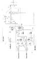
この種の従来の直流測定装置の一例を、図7に示す。
この直流測定装置は、測定対象である負荷に所望の電圧を印加してその負荷に流れる電流を測定するものであり、図7に示すように、測定対象である負荷4に印加すべき電圧を生成する電圧生成部1と、負荷4に流れる電流を設定値に制限する電流制限部2と、負荷4を接続する出力端子3と、を備えている(特許文献1参照)。An example of this type of conventional DC measuring apparatus is shown in FIG.
This direct current measuring device applies a desired voltage to a load to be measured and measures a current flowing through the load. As shown in FIG. 7, a voltage to be applied to the load 4 to be measured is measured. A voltage generation unit 1 to be generated, a current limiting unit 2 that limits a current flowing through the load 4 to a set value, and an
電圧生成部1は、D/A変換器(DAC)11、主増幅器12、インバータ13、電流検出抵抗14、バッファ回路15、および差動増幅器16などを備えている。
さらに詳述すると、D/A変換器11は、設定電圧を生成するための電圧に相当するデジタル値である設定電圧値をその値に応じたアナログ電圧に変換するものである。主増幅器12は、演算増幅器(オペアンプ)からなり、その非反転入力端子(+入力端子)にD/A変換器11から出力されるアナログ電圧が抵抗Riを介して供給されるようになっている。主増幅器12の反転入力端子(−入力端子)は、抵抗Rsを介して接地されている。主増幅器12の出力端子と反転入力端子との間には、コンデンサCsが接続されている。The voltage generation unit 1 includes a D / A converter (DAC) 11, a
More specifically, the D /
主増幅器12の出力端子は、インバータ(反転回路)13および電流検出抵抗14を介して出力端子3に接続されるとともに、その出力端子3は、バッファ回路15および帰還抵抗Rfを介して主増幅器12の非反転入力端子に接続されている。従って、主増幅器12は、負帰還増幅回路を構成している。
なお、主増幅器12は、その入力側にダイオードを互いに逆方向に並列接続した保護回路を備えている。The output terminal of the
The
電流検出抵抗14は、負荷4に流れる負荷電流(出力電流)Ioを検出するものであり、その両端が差動増幅器16の反転入力端子と非反転入力端子に接続されている。
電流制限部2は、D/A変換器21と、正側制限回路22と、D/A変換器23と、負側制限回路24とを備えている。
さらに詳述すると、D/A変換器21は、設定される正側の電流制限値と電流検出抵抗14の抵抗値とを掛け算した正の電圧を生成し、この正の電圧を出力するようになっている。The
The current limiting unit 2 includes a D /
More specifically, the D /
正側制限回路22は、図7に示すように、演算増幅器221と、入力抵抗R1p、R2pと、ダイオードD1pと、帰還抵抗R3pとから構成される。
演算増幅器221の反転入力端子には、入力抵抗R1pを介してD/A変換器21の出力電圧が供給されるとともに、入力抵抗R2pを介して差動増幅器16の出力電圧が供給されるようになっている。演算増幅器221の非反転入力端子は、接地されている。演算増幅器221の出力端子は、ダイオードD1pを介して主増幅器12の非反転入力端子に接続されている。また、演算増幅器221の出力端子は、ダイオードD1pおよび帰還抵抗R3pを介して演算増幅器221の反転入力端子に接続されている。As shown in FIG. 7, the positive
The output voltage of the D /
D/A変換器23は、設定される負側の電流制限値と電流検出抵抗14の抵抗値とを掛け算した負の電圧を生成し、この負の電圧を出力するようになっている。
負側制限回路24は、図7に示すように、演算増幅器241と、入力抵抗R1n、R2nと、ダイオードD1nと、帰還抵抗R3nとから構成される。
演算増幅器241の反転入力端子には、入力抵抗R1nを介してD/A変換器23の出力電圧が供給されるとともに、入力抵抗R2nを介して差動増幅器16の出力電圧が供給されるようになっている。演算増幅器241の非反転入力端子は、接地されている。演算増幅器241の出力端子は、ダイオードD1nを介して主増幅器12の非反転入力端子に接続されている。また、演算増幅器241の出力端子は、ダイオードD1nおよび帰還抵抗R3nを介して演算増幅器241の反転入力端子に接続されている。The D /
As shown in FIG. 7, the negative
The output voltage of the D /
次に、このような従来装置の動作例について、図7を参照して説明する。
まず、電圧生成部1が負荷4に所望の電圧を印加し、負荷4に流れる電流を測定する場合について説明する。
この場合には、主増幅器12は、出力端子3の出力電圧VoutがD/A変換器11の入力に設定される設定電圧値の設定電圧と等しくなるように動作し、その設定電圧が負荷4に印加される。このとき、負荷4に流れる負荷電流Ioが電流検出抵抗14に流れ、電流検出抵抗14の両端にはその負荷電流Ioに応じた電圧が発生する。そこで、差動増幅器16は、その負荷電流Ioの大きさに応じた電圧を取り出し、その電圧がA/D変換器(図示せず)でデジタル値に変換される。そして、そのデジタル値に基づいて負荷電流Ioが図示しない表示器などに表示される。Next, an operation example of such a conventional apparatus will be described with reference to FIG.
First, the case where the voltage generator 1 applies a desired voltage to the load 4 and measures the current flowing through the load 4 will be described.
In this case, the
次に、負荷4が例えばIC(集積回路)であって、そのICが故障している場合における電流制限部2の動作について説明する。
いま、負荷4に向かって流れる負荷電流Ioが過電流となり、差動増幅器16の負の出力電圧の絶対値がD/A変換器21の正の出力電圧よりも大きくなると、正側制限回路22の演算増幅器221の出力電圧が正電圧となる。この正電圧が逆流阻止用ダイオードD1pを通じ、さらに負帰還抵抗R3pを通じて演算増幅器221の反転入力端子に負帰還され、この反転入力端子の電圧がゼロになるように動作する。Next, the operation of the current limiting unit 2 when the load 4 is, for example, an IC (integrated circuit) and the IC has failed will be described.
Now, when the load current Io flowing toward the load 4 becomes an overcurrent, and the absolute value of the negative output voltage of the
ダイオードD1pと負帰還抵抗R3pの共通接続点は、差動増幅器16の出力電圧とD/A変換器21の出力電圧との差に応じた正電圧となり、この正電圧が主増幅器12の非反転入力端子に印加される。このため、インバータ13の出力電圧、すなわち出力端子3の出力電圧Voutが下がり、差動増幅器16の出力電圧の絶対値が、D/A変換器21の出力電圧と等しくなるように動作し、負荷電流IoはD/A変換器21に設定されている正電流制限値に制限(クランプ)される。
一方、負荷電流Ioがインバータ13側に向かう場合に、過電流になると、負側制限回路24が同様に動作し、負荷電流IoはD/A変換器23に設定されている負電流制限値に制限される。
On the other hand, when the load current Io goes to the
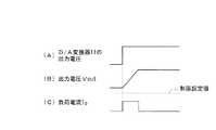
ところで、従来装置では、D/A変換器11の出力電圧が図8(A)に示すように変化し、これに応じて出力端子3の出力電圧Voutが変化する場合には、D/A変換器21、23から出力される正負の電流制限値に応じた正負の出力電圧の大小によって、電圧生成部1の出力電圧Voutのセトリング時間が異なるという不具合がある(図8(B)(C)参照)。 By the way, in the conventional apparatus, when the output voltage of the D /
例えば、正側制限回路22は、主増幅器12の非反転入力端子の電圧がVsであってD/A変換器21の正の出力電圧がVaとすると、Vs>Va×(−R3p/R1p)のときに制限ができるため、その値(Va×(−R3p/R1p))が電位Vsを超えると、正側制限回路22が動作してしまう。
この結果、正側制限回路22の制限電圧が低い場合には、それに応じて制限電圧値も下がり、その制限電圧が高い場合に比べて出力電圧Voutのスルーレート(セトリング時間)が長くなる(図8(B)(C)参照)。
ここで、図7における主増幅器12の最大スルーレートSRは、次の(1)式で表すことができる。
SR=Vs/Rs/Cs・・・(1)For example, the positive
As a result, when the limiting voltage of the positive
Here, the maximum slew rate SR of the
SR = Vs / Rs / Cs (1)
また、電圧生成部1の電圧生成時に、主増幅器12の入力に対する出力の過渡応答の指標である電圧セトリングが、以下の点で悪化する。
すなわち、負荷4は、バイパスコンデンサのようなコンデンサCLが並列に含まれる場合が一般的である。この場合には、D/A変換器11の出力電圧が図9(A)に示すように変化し、これによる出力電圧Voutの変化時に(図9(B)参照)、負荷4の他にコンデンサCLに電流が流れる。In addition, when the voltage generator 1 generates a voltage, voltage settling, which is an index of the transient response of the output with respect to the input of the
That is, the load 4 generally includes a capacitor CL such as a bypass capacitor in parallel. In this case, the output voltage of the D /
セトリング中に電流が供給される場合には、差動増幅器16の出力電圧をVbとすると、以下の制限が働く。
Vs>{Va×(−R3p/R1p)+Vb×(−R3p/R2p)}
この制限により、実際に決定した制限値より低い出力電流で制限がかかってしまう(図9(C)参照)。従って、正側制限回路22は、設定されている電流制限値よりも低い電流のときに電流制限動作を行うので、出力電圧Voutのセトリングが悪化するという不具合がある(図9(B)参照)。In the case where a current is supplied during settling, if the output voltage of the
Vs> {Va × (−R3p / R1p) + Vb × (−R3p / R2p)}
Due to this restriction, the restriction is applied at an output current lower than the actually determined restriction value (see FIG. 9C). Therefore, since the positive
従って、従来装置では、電圧生成部で所望の電圧を生成する際に、電流制限部に設定されている電流の設定制限値によってセトリング性能が悪化する場合があり、これは直流試験の高速化や高精度化にとって好ましいものではない。
そこで、本発明の目的は、上記の点に鑑み、電流などの測定時に、その電流の設定制限値によるセトリング性能を改善し、高速化、かつ高精度化に寄与できる直流測定装置を提供することにある。
また、本発明の他の目的は、その直流測定装置の上記の目的の実現に寄与できる制限回路を提供することにある。Therefore, in the conventional apparatus, when a desired voltage is generated by the voltage generation unit, the settling performance may be deteriorated due to the current setting limit value set in the current limiting unit. It is not preferable for high accuracy.
Therefore, in view of the above points, an object of the present invention is to provide a direct current measurement device that can improve the settling performance due to the current setting limit value when measuring current and the like, and can contribute to high speed and high accuracy. It is in.
Another object of the present invention is to provide a limiting circuit that can contribute to the realization of the above object of the DC measuring device.
上記の課題を解決し本発明の目的を達成するために、本発明は以下のような構成からなる。
第1の発明は、設定電圧に応じた電圧を出力する第1のD/A変換器と、前記第1のD/A変換器の出力電圧に基づいて前記設定電圧を生成してその設定電圧を負荷に供給する主増幅器と、前記負荷に流れる電流に応じた電圧を生成して出力する差動増幅器と、前記負荷に流れる所定の制限電流に応じた電圧を生成して出力する第2のD/A変換器と、前記差動増幅器の出力電圧と前記第2のD/A変換器の出力電圧との差を増幅し、これをダイオードを介して前記主増幅器の入力側に帰還する制限回路とを備え、前記制限回路は帰還抵抗を含む負帰還ループを有し、その負帰還ループは、前記制限回路の出力側にコンデンサおよびバッファ回路の双方を含むようにした。In order to solve the above problems and achieve the object of the present invention, the present invention has the following configuration.
According to a first aspect of the present invention, there is provided a first D / A converter that outputs a voltage corresponding to a set voltage, and the set voltage is generated based on an output voltage of the first D / A converter. A main amplifier that supplies a voltage to the load, a differential amplifier that generates and outputs a voltage according to the current flowing through the load, and a second amplifier that generates and outputs a voltage according to a predetermined limit current flowing through the load A limitation of amplifying the difference between the output voltage of the D / A converter and the differential amplifier and the output voltage of the second D / A converter and feeding this back to the input side of the main amplifier via a diode The limiting circuit has a negative feedback loop including a feedback resistor, and the negative feedback loop includesboth a capacitor and a buffer circuit on the output side of the limiting circuit.
第2の発明は、第1の発明において、前記制限回路のダイオードは、前記負帰還ループの一部を形成する第1のダイオードと、前記制限回路の出力を取り出す第2のダイオードと、からなる。 According to a second invention, in the first invention, the diode of the limiting circuit includes a first diode that forms a part of the negative feedback loop, and a second diode that extracts an output of the limiting circuit. .
第3の発明は、設定電圧に応じた電圧を出力する第1のD/A変換器と、前記第1のD/A変換器の出力電圧に基づいて前記設定電圧を生成してその設定電圧を負荷に供給する主増幅器と、前記負荷に流れる電流に応じた電圧を生成して出力する差動増幅器と、前記負荷に流れる所定の正および負の制限電流に応じた正および負の電圧をそれぞれ生成して出力する第2のD/A変換器および第3のD/A変換器と、前記差動増幅器の出力電圧と前記第2のD/A変換器の正の出力電圧との差を増幅し、これをダイオードを介して前記主増幅器の入力側に帰還する第1の制限回路と、前記差動増幅器の出力電圧と前記第3のD/A変換器の負の出力電圧との差を増幅し、これをダイオードを介して前記主増幅器の入力側に帰還する第2の制限回路と備え、前記第1および第2の制限回路は、帰還抵抗を含む第1および第2の負帰還ループをそれぞれ有し、その各負帰還ループは、前記各制限回路の出力側に共通のコンデンサおよび共通のバッファ回路のいずれか一方を含んでいる。According to athird aspect of the present invention, there is provided a first D / A converter that outputs a voltage corresponding to a set voltage, and the set voltage is generated based on an output voltage of the first D / A converter. A main amplifier that supplies a load to the load, a differential amplifier that generates and outputs a voltage according to the current flowing through the load, and a positive and negative voltage according to predetermined positive and negative limit currents flowing through the load. Second D / A converter and third D / A converter that generate and output, respectively, and the difference between the output voltage of the differential amplifier and the positive output voltage of the second D / A converter A first limiting circuit that feeds back to the input side of the main amplifier via a diode, an output voltage of the differential amplifier, and a negative output voltage of the third D / A converter A second limiting circuit amplifies the difference and feeds it back to the input side of the main amplifier through a diode. The first and second limiting circuits have first and second negative feedback loops each including a feedback resistor, and each negative feedback loop has a capacitor common to the output side of each limiting circuit. And any one of the common buffer circuits.
第4の発明は、設定電圧に応じた電圧を出力する第1のD/A変換器と、前記第1のD/A変換器の出力電圧に基づいて前記設定電圧を生成してその設定電圧を負荷に供給する主増幅器と、前記負荷に流れる電流に応じた電圧を生成して出力する差動増幅器と、前記負荷に流れる所定の正および負の制限電流に応じた正および負の電圧をそれぞれ生成して出力する第2のD/A変換器および第3のD/A変換器と、前記差動増幅器の出力電圧と前記第2のD/A変換器の正の出力電圧との差を増幅し、これをダイオードを介して前記主増幅器の入力側に帰還する第1の制限回路と、前記差動増幅器の出力電圧と前記第3のD/A変換器の負の出力電圧との差を増幅し、これをダイオードを介して前記主増幅器の入力側に帰還する第2の制限回路と備え、前記第1および第2の制限回路は、帰還抵抗を含む第1および第2の負帰還ループをそれぞれ有し、その各負帰還ループは、前記各制限回路の出力側に独立のコンデンサおよび独立のバッファ回路の双方を含んでいる。4th invention produces | generates the said setting voltage based on the 1st D / A converter which outputs the voltage according to a setting voltage, and the output voltage of the said 1st D / A converter, and the setting voltage A main amplifier that supplies a load to the load, a differential amplifier that generates and outputs a voltage according to the current flowing through the load, and a positive and negative voltage according to predetermined positive and negative limit currents flowing through the load. Second D / A converter and third D / A converter that generate and output, respectively, and the difference between the output voltage of the differential amplifier and the positive output voltage of the second D / A converter A first limiting circuit that feeds back to the input side of the main amplifier via a diode, an output voltage of the differential amplifier, and a negative output voltage of the third D / A converter A second limiting circuit amplifies the difference and feeds it back to the input side of the main amplifier through a diode. And wherein the first and second limiting circuit comprises a first and second negative feedback loop including a feedback resistor, respectively, the respective negative feedbackloop, independent of the capacitor the output side of the limiting circuit And an independent buffer circuit.
第5の発明は、第3または第4の発明において、前記第1の制限回路のダイオードは、前記第1の負帰還ループの一部を形成する第1のダイオードと、前記第1の制限回路の出力を取り出す第2のダイオードと、からなり、前記第2の制限回路のダイオードは、前記第2の負帰還ループの一部を形成する第3のダイオードと、前記第2の制限回路の出力を取り出す第4のダイオードと、からなる。According to afifth invention, in thethird orfourth invention, the diode of the first limiting circuit includes a first diode that forms a part of the first negative feedback loop, and the first limiting circuit. A second diode for taking out the output of the second limiting circuit, wherein the diode of the second limiting circuit is a third diode that forms part of the second negative feedback loop, and the output of the second limiting circuit a fourth diode to take out,Ru Tona.
第6の発明は、設定電流に応じた電圧を出力する第1のD/A変換器と、前記第1のD/A変換器の出力電圧に基づいて前記設定電流を生成してその設定電流を負荷に供給する主増幅器と、前記負荷の電圧を検出する電圧検出回路と、前記負荷に供給される所定の制限電圧を生成して出力する第2のD/A変換器と、前記電圧検出回路の検出電圧と前記第2のD/A変換器の出力電圧との差を増幅し、これをダイオードを介して前記主増幅器の入力側に帰還する制限回路とを備え、前記制限回路は帰還抵抗を含む負帰還ループを有し、その負帰還ループは、前記制限回路の出力側にコンデンサおよびバッファ回路の双方を含むようにした。According to asixth aspect of the present invention, there is provided a first D / A converter that outputs a voltage corresponding to a set current, and the set current is generated based on an output voltage of the first D / A converter. A main amplifier for supplying a load to the load, a voltage detection circuit for detecting a voltage of the load, a second D / A converter for generating and outputting a predetermined limit voltage supplied to the load, and the voltage detection A limiting circuit that amplifies a difference between a detection voltage of the circuit and an output voltage of the second D / A converter, and feeds back the amplified voltage to the input side of the main amplifier via a diode. A negative feedback loop including a resistor is included, and the negative feedback loop includesboth a capacitor and a buffer circuit on the output side of the limiting circuit.
第7の発明は、第6の発明において、前記制限回路のダイオードは、前記負帰還ループの一部を形成する第1のダイオードと、前記制限回路の出力を取り出す第2のダイオードと、からなる。Aseventh aspect of thesixth invention, the limiting circuit of the diode consists of a first diode which forms part of the negative feedback loop, and a second diode to take out the output of said limiting circuit, .
第8の発明は、設定電流に応じた電圧を出力する第1のD/A変換器と、前記第1のD/A変換器の出力電圧に基づいて前記設定電流を生成しその設定電流を負荷に供給する主増幅器と、前記負荷の電圧を検出する電圧検出回路と、前記負荷に供給される所定の制限電圧として正および負の電圧をそれぞれ生成して出力する第2のD/A変換器および第3のD/A変換器と、前記電圧検出回路の検出電圧と前記第2のD/A変換器の正の出力電圧との差を増幅し、これをダイオードを介して前記主増幅器の入力側に帰還する第1の制限回路と、前記電圧検出回路の検出電圧と前記第3のD/A変換器の負の出力電圧との差を増幅し、これをダイオードを介して前記主増幅器の入力側に帰還する第2の制限回路と備え、前記第1および第2の制限回路は、帰還抵抗を含む第1および第2の負帰還ループをそれぞれ有し、その各負帰還ループは、前記各制限回路の出力側に共通のコンデンサおよび共通のバッファ回路の双方を含んでいる。According to aneighth aspect of the present invention, a first D / A converter that outputs a voltage corresponding to a set current, the set current is generated based on an output voltage of the first D / A converter, and the set current is A main amplifier that supplies the load; a voltage detection circuit that detects the voltage of the load; and a second D / A converter that generates and outputs positive and negative voltages as predetermined limiting voltages supplied to the load. And a third D / A converter, amplifying a difference between a detection voltage of the voltage detection circuit and a positive output voltage of the second D / A converter, and this is amplified via a diode to the main amplifier A first limiting circuit that feeds back to the input side of the first and second amplifiers, and amplifies the difference between the detection voltage of the voltage detection circuit and the negative output voltage of the third D / A converter, and this is amplified via a diode. And a second limiting circuit that feeds back to the input side of the amplifier. Circuit has first and second negative feedback loop including a feedback resistor, respectively, the respective negative feedback loop includesboth the common capacitor and a common buffer circuit and the output side of the limiting circuit .
第9の発明は、設定電流に応じた電圧を出力する第1のD/A変換器と、前記第1のD/A変換器の出力電圧に基づいて前記設定電流を生成しその設定電流を負荷に供給する主増幅器と、前記負荷の電圧を検出する電圧検出回路と、前記負荷に供給される所定の制限電圧として正および負の電圧をそれぞれ生成して出力する第2のD/A変換器および第3のD/A変換器と、前記電圧検出回路の検出電圧と前記第2のD/A変換器の正の出力電圧との差を増幅し、これをダイオードを介して前記主増幅器の入力側に帰還する第1の制限回路と、前記電圧検出回路の検出電圧と前記第3のD/A変換器の負の出力電圧との差を増幅し、これをダイオードを介して前記主増幅器の入力側に帰還する第2の制限回路と備え、前記第1および第2の制限回路は、帰還抵抗を含む第1および第2の負帰還ループをそれぞれ有し、その各負帰還ループは、前記各制限回路の出力側に独立のコンデンサおよび独立のバッファ回路の双方を含んでいる。According to aninth aspect of the invention, a first D / A converter that outputs a voltage corresponding to a set current, and the set current is generated based on an output voltage of the first D / A converter, and the set current is A main amplifier that supplies the load; a voltage detection circuit that detects the voltage of the load; and a second D / A converter that generates and outputs positive and negative voltages as predetermined limiting voltages supplied to the load. And a third D / A converter, amplifying a difference between a detection voltage of the voltage detection circuit and a positive output voltage of the second D / A converter, and this is amplified via a diode to the main amplifier A first limiting circuit that feeds back to the input side of the first and second amplifiers, and amplifies the difference between the detection voltage of the voltage detection circuit and the negative output voltage of the third D / A converter, and this is amplified via a diode. And a second limiting circuit that feeds back to the input side of the amplifier. Circuit has first and second negative feedback loop including a feedback resistor, respectively, the respective negative feedback loopincludes both independent capacitors and independent of the buffer circuit to the output side of each of the limiting circuit .
第10の発明は、第8の発明または第9の発明において、前記第1の制限回路のダイオードは、前記第1の負帰還ループの一部を形成する第1のダイオードと、前記第1の制限回路の出力を取り出す第2のダイオードと、からなり、前記第2の制限回路のダイオードは、前記第2の負帰還ループの一部を形成する第3のダイオードと、前記第2の制限回路の出力を取り出す第4のダイオードと、からなる。In atenth aspect based on theeighth aspect or theninth aspect , the diode of the first limiting circuit includes a first diode forming a part of the first negative feedback loop, and the first diode. A second diode for extracting the output of the limiting circuit, the diode of the second limiting circuit being a third diode forming a part of the second negative feedback loop, and the second limiting circuit. a fourth diode extracting an output of,Ru Tona.
第11の発明は、所定の電圧を負荷に印加してその負荷の電流を測定する電流測定装置に使用される制限回路であって、演算増幅器と、前記演算増幅器の出力端子と反転入力端子との間に介在し、第1のダイオードおよび帰還抵抗を含む負帰還ループと、を備え、前記演算増幅器には、前記負荷の制限電流に応じた制限電圧と、前記負荷に流れる電流に応じて得られる検出電圧とを入力するようにし、前記負帰還ループは、前記演算増幅器の出力側にコンデンサおよびバッファ回路の双方を含むようにした。
第12の発明は、第11の発明において、前記演算増幅器の出力は、第2のダイオードを介して取り出すようにした。Aneleventh invention is a limiting circuit used in the current measuring device for measuring the current of the load by applying a predetermined voltage to a load, an operational amplifier and an output terminal and theinverting input terminal of the operational amplifier A negative feedback loop including a first diode and a feedback resistor, and the operational amplifier includes a limit voltage according to a limit current of the load and a current flowing through the load. The obtained detection voltage is input, and the negative feedback loop includesboth a capacitor and a buffer circuit on the output side of the operational amplifier.
In atwelfth aspect based on theeleventh aspect , the output of the operational amplifier is extracted via a second diode.
本発明の直流測定装置によれば、電流などの測定時に、その電流の設定制限値によるセトリング性能を改善し、高速化、かつ高精度化に寄与することができる。
また、本発明の制限回路によれば、本発明の直流測定装置の上記の効果の実現に寄与することができる。According to the direct current measuring device of the present invention, at the time of measuring a current or the like, it is possible to improve the settling performance due to the set limit value of the current, thereby contributing to speeding up and high accuracy.
Moreover, according to the limiting circuit of the present invention, it is possible to contribute to the realization of the above-described effect of the direct current measuring device of the present invention.
以下、本発明の実施の形態を、図面を参照して説明する。
(第1実施形態)
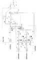
本発明の直流測定装置に係る第1実施形態は、測定対象である負荷に所望の電圧を印加してその負荷に流れる電流を測定するものであり、図1に示すように、測定対象である負荷4に印加すべき電圧を生成する電圧生成部1と、負荷4に流れる電流を設定値に制限する電流制限部6と、負荷4を接続する出力端子3と、を備えている。Hereinafter, embodiments of the present invention will be described with reference to the drawings.
(First embodiment)
1st Embodiment which concerns on the direct current | flow measuring apparatus of this invention applies a desired voltage to the load which is a measuring object, and measures the electric current which flows into the load, and is a measuring object as shown in FIG. A voltage generation unit 1 that generates a voltage to be applied to the load 4, a current limiting
電圧生成部1は、D/A変換器11、主増幅器12、インバータ13、電流検出抵抗14、バッファ回路15、および差動増幅器16などを備えている。ここで、この電圧生成部1の各構成要素は、図7に示す電圧生成部1の同一符号を付した各構成要素とその構成が基本的に同様であるので、その説明は省略する。
電流制限部6は、D/A変換器61と、正側制限回路62と、D/A変換器63と、負側制限回路64と、を備えている。ここで、正側制限回路62や負側制限回路64は、本発明の制限回路に対応する。The voltage generator 1 includes a D /
The current limiting
さらに詳述すると、D/A変換器61は、設定される正側の電流制限値と電流検出抵抗14の抵抗値とを掛け算した正の電圧を生成し、この正の電圧を出力するようになっている。
正側制限回路62は、差動増幅器16の出力電圧とD/A変換器61の出力電圧との差の電圧を増幅し、これをダイオードD1pおよびダイオードDc1を介して主増幅器12の非反転入力端子に帰還し、負荷4に流れる電流を正の電流制限値に制限するようになっている。More specifically, the D /
The positive
このために、正側制限回路62は、図1に示すように、演算増幅器621と、入力抵抗R1p、R2pと、逆流防止用のダイオードD1pと、帰還抵抗R3pと、直流遮断用のコンデンサCcと、入力インピーダンスが高いバッファ回路65と、ダイオードDc1と、を備えている。ここで、正側制限回路62において、ダイオードD2pは省略するようにしても良い。 For this reason, as shown in FIG. 1, the positive
演算増幅器621の反転入力端子には、入力抵抗R1pを介してD/A変換器61の出力電圧V4が供給されるとともに、入力抵抗R2pを介して差動増幅器16の出力電圧V5が供給されるようになっている。演算増幅器621の非反転入力端子は、接地されている。
演算増幅器621の出力端子は、ダイオードD1pおよびダイオードDc1を介して主増幅器12の非反転入力端子に接続されている。また、演算増幅器621の出力端子は、ダイオードD1p、バッファ回路65、コンデンサCc、および帰還抵抗R3pを介して演算増幅器621の反転入力端子に接続されている。従って、正側制限回路62は負帰還ループ(負帰還ループ回路)を有し、その負帰還ループは、帰還抵抗R3pの他に、コンデンサCcとバッファ回路65を含んでいる。The output voltage V4 of the D /
The output terminal of the
D/A変換器63は、設定される負側の電流制限値と電流検出抵抗14の抵抗値とを掛け算した負の電圧を生成し、この負の電圧を出力するようになっている。
負側制限回路64は、差動増幅器16の出力電圧とD/A変換器63の出力電圧との差の電圧を増幅し、これをダイオードD1nおよびダイオードDc2を介して主増幅器12の非反転入力端子に帰還し、負荷4に流れる電流を負の電流制限値に制限するようになっている。
このために、負側制限回路64は、図1に示すように、演算増幅器641と、入力抵抗R1n、R2nと、逆流防止用のダイオードD1nと、帰還抵抗R3nと、直流遮断用のコンデンサCcと、入力インピーダンスが高いバッファ回路65と、ダイオードDc2と、を備えている。ここで、負側制限回路64において、ダイオードD2nは省略するようにしても良い。The D /
The negative
Therefore, as shown in FIG. 1, the negative
演算増幅器641の反転入力端子には、入力抵抗R1nを介してD/A変換器63の出力電圧が供給されるとともに、入力抵抗R2nを介して差動増幅器16の出力電圧が供給されるようになっている。演算増幅器641の非反転入力端子は、接地されている。
演算増幅器641の出力端子は、ダイオードD1nおよびダイオードDc2を介して主増幅器12の非反転入力端子に接続されている。また、演算増幅器641の出力端子は、ダイオードD1n、バッファ回路65、コンデンサCc、および帰還抵抗R3nを介して演算増幅器641の反転入力端子に接続されている。従って、負側制限回路64は負帰還ループを有し、その負帰還ループは、帰還抵抗R3nの他に、コンデンサCcとバッファ回路65を含んでいる。The output voltage of the D /
The output terminal of the
ここで、バッファ回路65の非反転入力端子は、例えば高抵抗からなる抵抗Rbによって主増幅器12の非反転入力端子に接続されている。これは、制限回路62、64が制限動作をしないときに、バッファ回路65の非反転入力端子の電位が不定にならないように所定の電位に固定させるためである。
なお、正側制限回路62および負制限回路64は、いずれか一方が動作するようになっている。このため、正側制限回路62および負側制限回路64は、その負帰還ループ回路内にコンデンサCcとバッファ回路65を共有している。Here, the non-inverting input terminal of the
Note that either the
次に、このような構成からなる第1実施形態の動作例について、図面を参照して説明する。
まず、電圧生成部1が負荷4に所望の電圧を印加し、負荷4に流れる電流を測定する場合の動作は、図7の場合と同様であるので、その説明は省略する。
次に、ICなどの負荷4が故障し、負荷4に流れる電流が過電流の場合における電流制限部6の動作について説明する。
いま、負荷4に向かって流れる負荷電流Ioが過電流となり、差動増幅器16の負の出力電圧の絶対値がD/A変換器61の正の出力電圧よりも大きくなると、正側制限回路62の演算増幅器621の出力電圧が正電圧となる。この正電圧がダイオードD1pを通じ、さらにバッファ回路65、コンデンサCc、および負帰還抵抗R3pを通じて演算増幅器621の反転入力端子に負帰還され、この反転入力端子の電圧がゼロになるように動作する。Next, an operation example of the first embodiment having such a configuration will be described with reference to the drawings.
First, the operation when the voltage generator 1 applies a desired voltage to the load 4 and measures the current flowing through the load 4 is the same as in FIG.
Next, the operation of the current limiting
If the load current Io flowing toward the load 4 becomes an overcurrent, and the absolute value of the negative output voltage of the
ダイオードD1pとバッファ回路65の非反転入力端子の共通接続点は、差動増幅器16の出力電圧とD/A変換器61の出力電圧との差に応じた正電圧となり、この正電圧がダイオードDc1を介して主増幅器12の非反転入力端子に印加される。このため、インバータ13の出力電圧、すなわち出力端子3の出力電圧Voutが下がり、差動増幅器16の出力電圧の絶対値が、D/A変換器61の出力電圧と等しくなるように動作し、負荷電流IoはD/A変換器61に設定されている正電流制限値に制限(クランプ)される。
一方、負荷電流Ioがインバータ13側に向かう場合に、過電流になると、負側制限回路64が同様に動作し、負荷電流IoはD/A変換器63に設定されている負電流制限値に制限される。The common connection point between the diode D1p and the non-inverting input terminal of the
On the other hand, when the load current Io is directed to the
次に、この第1実施形態では、D/A変換器11の出力電圧が図2(A)に示すように変化する場合に、出力端子3の出力電圧Voutが図2(C)に示すように変化し、電流制限部6に設定される電流制限値の小さな場合に電圧生成部1のスルーレートが改善されるので、この点について、正側制限回路62側の動作を例に説明する。
この第1実施形態においても、最大スルーレートSRは上記の(1)式で表すことができ、最大スルーレートを発揮するときには、主増幅器12の非反転入力端子の電位Vsは、Vs=−VFとなる。ここで、VFは、ダイオードDc1の順方向電圧降下である。Next, in the first embodiment, when the output voltage of the D /
Also in the first embodiment, the maximum slew rate SR can be expressed by the above equation (1). When the maximum slew rate is exhibited, the potential Vs of the non-inverting input terminal of the
正側制限回路62では、帰還抵抗R3pとコンデンサCcとの接続点の電位V1は、V4×(−R3p/R1p)で制限される。ここで、V4は、D/A変換器61の出力電圧であり、正電流制限値に応じたものである。
このため、その電位V1がV1>V2の関係になると、正側制限回路62が動作することになり、これにより主増幅器12の非反転入力端子の電圧Vsが制限され、結果的に上記の出力電圧Voutのスルーレートが制限される。なお、V2はバッファ回路65の出力端子の電位であって、そのバッファ回路65の非反転入力端子の電位V3と等しい。
ところで、そのスルーレートが発生している間に正側制限回路62を動作させないためには、常時、V1≦V2の関係を満たす必要がある。In the positive
For this reason, when the potential V1 is in the relationship of V1> V2, the positive
By the way, in order not to operate the positive
ダイオードDc1がない場合には、D/A変換器61の出力電圧V4の値によってV1>V2になる場合がある。しかし、ダイオードDc1がある場合には、正側制限回路62が動作しようとした場合に、ダイオードD1pがオンしようとすると、そのダイオードDc1の順方向電圧降下VFによって、バッファ回路65の反転入力端子の電位V3は、V3=Vs+VFとなり、順方向電圧降下VFの分だけ増加する。このため、D/A変換器61の出力電圧による電位Vsの制限範囲(0〜V4×(−R3p/R1p))が、V3=Vs+VFを上回らなければ、正側制限回路62は動作しない。 When there is no diode Dc1, V1> V2 may be satisfied depending on the value of the output voltage V4 of the D /
以上の説明は、正側制限回路62側の例であるが、これらの動作は負側制限回路64側の場合も同様である。
従って、この第1実施形態では、D/A変換器61、63の設定電流制限値を超えない場合には、その設定電流制限値の大小、すなわちD/A変換器61,63の出力電圧の大小にかかわらず、電圧生成部1のスルーレートは変化せずに同じになる。
このため、この第1実施形態によれば、電圧生成部1の出力電圧Voutは、D/A変換器61、63の設定電流制限値の小さな場合には図2(C)に示すようになり、電流制限値の小さな場合に従来に比べてスルーレートが改善されることがわかる。The above description is an example on the positive
Therefore, in the first embodiment, when the set current limit value of the D /
Therefore, according to the first embodiment, the output voltage Vout of the voltage generator 1 is as shown in FIG. 2C when the set current limit values of the D /
次に、この第1実施形態において、D/A変換器11の出力電圧が図3(A)に示すように変化し、このときに出力端子3に負荷4が接続されていたり、またはその負荷4がコンデンサCLを含む場合の動作について説明する。
この場合には、そのD/A変換器11の出力電圧の変化に伴い、出力端子3の出力電圧Voutが図3(B)のように変化し、スルーレートがある。これに伴い、電流検出抵抗14に負荷電流Ioが流れ、これにより差動増幅器16の出力電圧はV5となる。正側制限回路62は、D/A変換器61の出力電圧V4と差動増幅器16の出力電圧V5の電圧比較によって動作しようとする。Next, in the first embodiment, the output voltage of the D /
In this case, as the output voltage of the D /
しかし、正側制限回路62は、その負帰還ループ内にバッファ回路65とコンデンサCcを含んでいる。このため、そのスルーレートの発生中に主増幅器12の非反転入力端子に電位Vsが発生しても、その電位Vsによる帰還抵抗R3pの電流発生を防止することができる。
このため、正側制限回路62は、抵抗R1p、R2p、設定制限電流値に応じたD/A変換器61の出力電圧V4、および差動増幅器16の出力電圧(負荷電流Io)だけで電流制限が決定される。However, the positive
For this reason, the positive
従って、スルーレートの発生中(セトリング中)に、図3(C)に示すような負荷電流Ioが流れても、正側制限回路62は、その負荷電流Ioが設定制限電流値を超えない限り電流制限動作を行わない。これらの事情は、D/A変換器63および負側制限回路64側においても同様である。
このため、この第1実施形態では、スルーレートの発生中において、電流制限部6の制限電流値が設定値以下の場合には、従来のように電流制限動作がないので、出力電圧Voutは図3(B)のような波形となってスルーレートの改善が図られる。Therefore, even if the load current Io as shown in FIG. 3C flows during the generation of the slew rate (during settling), the positive
For this reason, in the first embodiment, when the limit current value of the
次に、第1実施形態の特徴的な構成と、それに伴う作用効果をまとめると以下のようになる。
(1)第1実施形態では、正側制限回路62および負側制限回路64が、その各負帰還ループ内に直流を遮断するためのコンデンサCcを含むようにした。このため、D/A変換器11の出力電圧の変化によって出力電圧Voutがスルーレートを発生するときに、主増幅器12の非反転入力端子の電位VsがD/A変換器61、63の設定電流制限値に対応する出力電圧に影響されなくなる。従って、第1実施形態によれば、正側制限回路62および負側制限回路64のゲインを高めることができ、より高速でかつ高精度な電流制限動作が実現可能となる。Next, the characteristic configuration of the first embodiment and the operational effects associated therewith are summarized as follows.
(1) In the first embodiment, the positive
(2)また、第1実施形態では、正側制限回路62および負側制限回路64が、その各負帰還ループ内にバッファ回路65を設け、これによりその負帰還ループに電流が流れないようにした。このため、第1実施形態によれば、等価的に正側制限回路62および負側制限回路64の各入力インピーダンスを高めることができ、もって電圧生成部1の帰還量の減衰を防止でき、この結果、電圧生成部1の周波数特性を改善し、セトリング特性の改善を図ることができる。(2) Further, in the first embodiment, the positive
(3)さらに、第1実施形態では、正側制限回路62および負側制限回路64は、その各出力電圧をダイオードDc1、Dc2を介して主増幅器12の非反転入力端子にそれぞれ供給するようにした。このため、第1実施形態では、スルーレートの発生中に、バッファ回路65の非反転入力端子に流れる電流(正電圧スルーレート時には吸い込み電流、負電圧スルーレート時には吐き出し電流)を防止し、正側制限回路62および負側制限回路64の電流制限動作は行わない。従って、第1実施形態では、負荷電流Ioが設定電流制限値を超えない場合には電流制限動作を行わないので、設定電流制限値の大小にかかわらず電圧セトリングが変化せずに同じになる。(3) Furthermore, in the first embodiment, the positive
(4)なお、第1実施形態では、制限回路62、64の各負帰還ループはコンデンサCcおよびバッファ回路65を含み、さらに制限回路62、64の出力はダイオードDc1、Dc2を介して取り出すようにした。
しかし、本発明は、これらを全て含む必要はなく、少なくともそのうちの1つを含んでいれば良く、あるいはコンデンサCcとバッファ回路65の組み合わせや、コンデンサCcとダイオードDc1、Dc2の組み合わせなどであっても良い。これらの点は、以下の各実施形態の場合も同様である。(4) In the first embodiment, each negative feedback loop of the limiting
However, the present invention does not need to include all of them, and may include at least one of them, or a combination of the capacitor Cc and the
(第2実施形態)
図1に示す第1実施形態では、正側制限回路62と負側制限回路64はいずれか一方が動作して同時に動作することはないので、正側制限回路62および負側制限回路64の各負帰還ループは、コンデンサCcを共有するようにした。
しかし、この場合には、コンデンサCcを共有するので、正側制限回路62と負側制限回路64の各特性を、コンデンサCcの値によって異ならせることができない。
そこで、本発明の測定装置に係る第2実施形態は、図1に示す第1実施形態の構成を基本とし、図4に示すように、正側制限回路62および負側制限回路64の各負帰還ループがコンデンサCc1、Cc2を独立して含むようにし、コンデンサCc1、Cc2の容量値によって正側制限回路62および負側制限回路64が、必要に応じて、それぞれ任意の特性を得られるようにしたものである。(Second Embodiment)
In the first embodiment shown in FIG. 1, since either one of the positive
However, in this case, since the capacitor Cc is shared, the characteristics of the positive
Therefore, the second embodiment according to the measuring apparatus of the present invention is based on the configuration of the first embodiment shown in FIG. 1, and each of the negative
すなわち、正側制限回路62の負帰還ループは、帰還抵抗R3pの他に独立のコンデンサCc1を含むようにした。コンデンサCc1の一端側は帰還抵抗R3pに接続され、その他端側はバッファ回路65の出力端子に接続されている。また、負側制限回路64の負帰還ループは、帰還抵抗R3nの他に独立のコンデンサCc2を含むようにした。このコンデンサCc2の一端側は帰還抵抗R3nに接続され、その他端側はバッファ回路65の出力端子に接続されている。
なお、この第2実施形態では、上記の構成を除く他の部分の構成は、図1の第1実施形態の構成と同一であるので、同一の構成要素には同一符号を付してその詳細な説明は省略する。
このような構成からなる第2実施形態によれば、第1実施形態と同様の作用、効果を実現できる。That is, the negative feedback loop of the positive
In the second embodiment, the configuration of the other parts other than the above configuration is the same as the configuration of the first embodiment in FIG. The detailed explanation is omitted.
According to 2nd Embodiment which consists of such a structure, the effect | action and effect similar to 1st Embodiment are realizable.
(第3実施形態)
本発明の測定装置に係る第3実施形態は、図1に示す第1実施形態の構成を基本とし、図5に示すように、正側制限回路62および負側制限回路64の各負帰還ループが、コンデンサCc1、Cc2を独立して含むとともに、バッファ回路65A、65Bを独立して含むようにしたものである。
すなわち、正側制限回路62の負帰還ループは、帰還抵抗R3pの他に、独立のコンデンサCc1とバッファ回路65Aとを含むようにした。コンデンサCc1の一端側は帰還抵抗R3pに接続され、その他端側はバッファ回路65Aの出力端子に接続されている。また、バッファ回路65Aの非反転入力端子は、ダイオードD1pのカソードに接続されている。(Third embodiment)
The third embodiment according to the measuring apparatus of the present invention is based on the configuration of the first embodiment shown in FIG. 1, and each negative feedback loop of the positive
That is, the negative feedback loop of the positive
また、負側制限回路64の負帰還ループは、帰還抵抗R3nの他に、独立のコンデンサCc2とバッファ回路65Bとを含むようにした。コンデンサCc2の一端側は帰還抵抗R3nに接続され、その他端側はバッファ回路65Bの出力端子に接続されている。さらに、バッファ回路65Bの非反転入力端子は、ダイオードD1nのアノードに接続されている。
なお、この第3実施形態では、上記の構成を除く他の部分の構成は、図1の第1実施形態の構成と同一であるので、同一の構成要素には同一符号を付してその詳細な説明は省略する。Further, the negative feedback loop of the negative
In the third embodiment, the configuration of the other parts other than the above configuration is the same as the configuration of the first embodiment in FIG. The detailed explanation is omitted.
このような構成からなる第3実施形態によれば、正側制限回路62および負側制限回路64の各負帰還ループを独立に構成できるので、正側制限回路62および負側制限回路64の各特性を必要に応じて任意に設定できる上に、その各特性の影響を排除できる。
また、第3実施形態によれば、第1実施形態と同様の作用、効果を実現できる。According to the third embodiment having such a configuration, since the negative feedback loops of the positive
Further, according to the third embodiment, the same operation and effect as the first embodiment can be realized.
(第4実施形態)
本発明の測定装置に係る第4実施形態は、測定対象である負荷に所望の電流を供給してそのときの負荷の電圧を測定するものであり、図6に示すように、測定対象である負荷4に供給すべき電流を生成する電流生成部7と、そのときの負荷4の電圧を設定値に制限する電圧制限部8と、負荷4を接続する出力端子3と、を備えている。
電流生成部7は、図6に示すように、D/A変換器71、主増幅器72、インバータ73、電流検出抵抗74、差動増幅器75、バッファ回路76、およびインバータ77などを備えている。ここで、バッファ回路76とインバータ77が、出力電圧Voutを検出する電圧検出回路を構成する。(Fourth embodiment)
The fourth embodiment according to the measuring apparatus of the present invention supplies a desired current to a load that is a measurement target and measures the voltage of the load at that time, and is a measurement target as shown in FIG. A current generation unit 7 that generates a current to be supplied to the load 4, a voltage limiting unit 8 that limits the voltage of the load 4 at that time to a set value, and an
As shown in FIG. 6, the current generation unit 7 includes a D /
さらに詳述すると、D/A変換器71は、設定電流値をその値に応じたアナログ電圧に変換するものである。主増幅器72は、演算増幅器からなり、その非反転入力端子にD/A変換器71から出力されるアナログ電圧が抵抗Riを介して供給されるようになっている。主増幅器72の反転入力端子は、抵抗Rsを介して接地されている。また、主増幅器72の出力端子と反転入力端子との間には、コンデンサCsが接続されている。 More specifically, the D /
主増幅器72の出力端子は、インバータ(反転回路)73および電流検出抵抗74を介して出力端子3に接続されている。電流検出抵抗74は、負荷4に流れる電流Ioを検出するものであり、その両端が差動増幅器75の反転入力端子と非反転入力端子に接続されている。差動増幅器75の出力端子は、帰還抵抗Rfを介して主増幅器72の非反転入力端子に接続されている。従って、主増幅器72は、負帰還増幅回路を構成している。 The output terminal of the
バッファ回路76は、出力端子3の出力電圧Vout(負荷4の電圧)を検出し、この検出電圧はインバータ77で反転されて、後述の正側制限回路82および負側制限回路84の入力側に供給されるようになっている。
電圧制限部8は、D/A変換器81と、正側制限回路82と、D/A変換器83と、負側制限回路84とを備えている。
さらに詳述すると、D/A変換器81は、設定される正側の電圧制限値に応じた正の電圧を生成し、この正の電圧を出力するようになっている。The
The voltage limiting unit 8 includes a D /
More specifically, the D /
正側制限回路82は、インバータ77の出力電圧とD/A変換器81の出力電圧との差の電圧を増幅し、これをダイオードD1pおよびダイオードDc1を介して主増幅器72の非反転入力端子に帰還し、負荷4の電圧を正の電圧制限値に制限するようになっている。
このために、正側制限回路82は、図6に示すように、演算増幅器821と、入力抵抗R1p、R2pと、ダイオードD1pと、帰還抵抗R3pと、直流遮断用のコンデンサCc1と、入力インピーダンスが高いバッファ回路85Aと、ダイオードDc1と、を備えている。ここで、正側制限回路82において、ダイオードD2pは省略するようにしても良い。The positive
Therefore, as shown in FIG. 6, the positive
演算増幅器821の反転入力端子には、入力抵抗R1pを介してD/A変換器81の出力電圧が供給されるとともに、入力抵抗R2pを介してインバータ77の出力電圧が供給されるようになっている。また、演算増幅器821の非反転入力端子は、接地されている。
演算増幅器821の出力端子は、ダイオードD1pおよびダイオードDc1を介して主増幅器12の非反転入力端子に接続されている。また、演算増幅器821の出力端子は、ダイオードD1p、バッファ回路85A、コンデンサCc1、および帰還抵抗R3pを介して演算増幅器821の反転入力端子に接続されている。従って、正側制限回路82は負帰還ループを有し、その負帰還ループは、帰還抵抗R3pの他に、コンデンサCc1とバッファ回路85Aを含んでいる。The output voltage of the D /
The output terminal of the
D/A変換器83は、設定される負側の電圧制限値に応じた負の電圧を生成し、この負の電圧を出力するようになっている。
負側制限回路84は、インバータ77の出力電圧とD/A変換器83の出力電圧との差の電圧を増幅し、これをダイオードD1nおよびダイオードDc2を介して主増幅器72の非反転入力端子に帰還し、負荷4の電圧を負の電圧制限値に制限するようになっている。
このために、負側制限回路84は、図6に示すように、演算増幅器841と、入力抵抗R1n、R2nと、ダイオードD1nと、帰還抵抗R3nと、直流遮断用のコンデンサCc2と、入力インピーダンスが高いバッファ回路85Bと、ダイオードDc2と、を備えている。ここで、負側制限回路84において、ダイオードD2nは省略するようにしても良い。The D /
The negative
For this reason, as shown in FIG. 6, the negative
演算増幅器841の反転入力端子には、入力抵抗R1nを介してD/A変換器83の出力電圧が供給されるとともに、入力抵抗R2nを介してインバータ77の出力電圧が供給されるようになっている。また、演算増幅器841の非反転入力端子は、接地されている。
演算増幅器841の出力端子は、ダイオードD1nおよびダイオードDc2を介して主増幅器72の非反転入力端子に接続されている。また、演算増幅器841の出力端子は、ダイオードD1n、バッファ回路85B、コンデンサCc2、および帰還抵抗R3nを介して演算増幅器841の反転入力端子に接続されている。従って、負側制限回路84は負帰還ループを有し、その負帰還ループは、帰還抵抗R3nの他に、コンデンサCc2とバッファ回路85Bを含んでいる。
ここで、バッファ回路85A、85Bの非反転入力端子は、例えば高抵抗からなる抵抗Rbによって主増幅器72の非反転入力端子に接続されている。これは、制限回路82、84が制限動作をしないときに、バッファ回路85A、85Bの非反転入力端子の電位が不定にならないように所定の電位に固定させるためである。The output voltage of the D /
The output terminal of the
Here, the non-inverting input terminals of the
次に、このような構成からなる第4実施形態の動作例について、図面を参照して説明する。
まず、電流生成部7で生成する所望の電流を負荷4に供給し、このときの負荷4の電圧を測定する場合について説明する。
この場合には、D/A変換器71は、設定電流に対応するアナログ電圧に変換し、そのアナログ電圧を主増幅器72の非反転入力端子に供給する。これにより、電流検出抵抗74に負荷電流Ioが流れ、その両端には負荷電流Ioに応じた電圧が発生する。この電圧は差動増幅器75で増幅され、差動増幅器75の出力電圧が主増幅器72の反転入力端子に帰還され、負荷電流Ioが設定電流に等しくなるように動作する。
バッファ回路76には、負荷4の電圧(出力端子3の電圧)が入力され、この電圧をバッファ回路76から取り出し、この取り出した電圧がA/D変換器(図示せず)でデジタル値に変換される。そして、そのデジタル値が、負荷4の電圧として図示しない表示器などに表示される。Next, an operation example of the fourth embodiment having such a configuration will be described with reference to the drawings.
First, a case where a desired current generated by the current generator 7 is supplied to the load 4 and the voltage of the load 4 at this time is measured will be described.
In this case, the D /
The voltage of the load 4 (voltage of the output terminal 3) is input to the
次に、負荷4がオープンとなり、正の負荷電圧(出力端子3の電圧)が過電圧の場合における電圧制限部8の動作について説明する。
いま、バッファ回路76で検出されてインバータ77で反転された負の出力電圧の絶対値がD/A変換器81の正の出力電圧よりも大きくなると、正側制限回路82の演算増幅器821の出力電圧が正電圧となる。この正電圧がダイオードD1pを通じ、さらにバッファ回路85A、コンデンサCc1、および負帰還抵抗R3pを通じて演算増幅器821の反転入力端子に負帰還され、この反転入力端子の電圧がゼロになるように動作する。Next, the operation of the voltage limiting unit 8 when the load 4 is open and the positive load voltage (the voltage at the output terminal 3) is an overvoltage will be described.
Now, when the absolute value of the negative output voltage detected by the
ダイオードD1pとバッファ回路85Aの非反転入力端子の共通接続点は、インバータ77の出力電圧とD/A変換器81の出力電圧との差に応じた正電圧となり、この正電圧がダイオードDc1を介して主増幅器72の非反転入力端子に印加される。このため、インバータ73の出力電圧、すなわち出力端子3の出力電圧Voutが下がり、バッファ回路76の出力電圧の絶対値が、D/A変換器81の出力電圧と等しくなるように動作し、負荷電圧はD/A変換器81に設定されている正の電圧制限値に制限される。 The common connection point between the diode D1p and the non-inverting input terminal of the
一方、出力端子3が負の過電圧になった場合には、負側制限回路84が同様に動作し、出力端子3の電圧はD/A変換器83に設定されている負の電圧制限値に制限される。
なお、第4実施形態では、第1実施形態の場合と同様に、D/A変換器71の出力電圧が変化する場合に、出力端子3の出力電圧Voutが変化し、電圧制限部8に設定される電圧制限値の小さな場合に、電流生成部7のスルーレートが改善される。On the other hand, when the
In the fourth embodiment, as in the case of the first embodiment, when the output voltage of the D /
この場合の正側制限回路82などの動作原理は、第1実施形態の正側制限回路62などの動作原理と同様であるので、その説明は省略する。
また、第4実施形態において、第1実施形態の場合と同様に、出力端子3に接続される負荷4がコンデンサCLを含む場合に、スルーレートの改善が図られる。この場合の正側制限回路82などの動作原理も、第1実施形態の正側制限回路62などの動作原理と同様であるので、その説明は省略する。In this case, the operating principle of the positive-
Further, in the fourth embodiment, as in the case of the first embodiment, when the load 4 connected to the
次に、この第4実施形態の特徴的な構成と、それに伴う作用効果をまとめると以下のようになる。
(1)第4実施形態では、正側制限回路82および負側制限回路84が、その各負帰還ループ内に直流を遮断するためのコンデンサCc1、CC2を含むようにした。このため、D/A変換器71の出力電圧の変化によって出力電圧Voutが変化してスルーレートを発生するときに、主増幅器72の非反転入力端子の電位VsがD/A変換器81、83の設定電流制限値に対応する出力電圧に影響されなくなる。従って、第4実施形態によれば、正側制限回路82および負側制限回路84のゲインを高めることができ、より高速でかつ高精度な電圧制限動作が実現可能となる。Next, the characteristic configuration of the fourth embodiment and the operational effects associated therewith are summarized as follows.
(1) In the fourth embodiment, the positive-
(2)また、第4実施形態では、正側制限回路82および負側制限回路84が、その各負帰還ループ内にバッファ回路85A、85Bを設け、これによりその負帰還ループに電流が流れないようにした。このため、第4実施形態によれば、等価的に正側制限回路82および負側制限回路84の各入力インピーダンスを高めることができ、もって電流生成部7の帰還量の減衰を防止でき、この結果、電流生成部7の周波数特性を改善し、セトリング特性の改善を図ることができる。(2) In the fourth embodiment, the positive-
(3)さらに、第4実施形態では、正側制限回路82および負側制限回路84は、その各出力電圧をダイオードDc1、Dc2を介して主増幅器72の非反転入力端子にそれぞれ供給するようにした。このため、第4実施形態では、スルーレートの発生中に、バッファ回路85A、85Bの非反転入力端子に流れる電流(正電圧スルーレート時には吸い込み電流、負電圧スルーレート時には吐き出し電流)を防止し、正側制限回路82および負側制限回路84の電圧制限動作は行わない。従って、第4実施形態では、負荷4の電圧が設定電圧制限値を超えない場合には電圧制限動作を行わないので、設定電圧制限値の大小にかかわらず電圧セトリングが変化せずに同じになる。(3) Further, in the fourth embodiment, the positive-
(4)また、第4実施形態では、正側制限回路82および負側制限回路84の各負帰還ループを独立に構成するようにしたので、正側制限回路82および負側制限回路84特性を必要に応じてそれぞれ任意に設定できる上に、その各特性の影響を排除できる。
(5)なお、第4実施形態では、制限回路82、84の各負帰還ループはコンデンサCc1、Cc2およびバッファ回路85A、85Bを含み、さらに制限回路82、84の出力はダイオードDc1、Dc2を介して取り出すようにした。
しかし、本発明は、これらを全て含む必要はなく、少なくともそのうちの1つを含んでいれば良く、あるいはコンデンサCc1、Cc2とバッファ回路85A、85Bの組み合わせや、コンデンサCcc1、Cc2とダイオードDc1、Dc2の組み合わせなどであっても良い。(4) In the fourth embodiment, since the negative feedback loops of the positive
(5) In the fourth embodiment, each of the negative feedback loops of the limiting
However, the present invention does not need to include all of them, and may include at least one of them, or a combination of capacitors Cc1 and Cc2 and
1 電圧生成部
3 出力端子
4 負荷(測定対象)
6 電流制限部
7 電流生成部
8 電圧制限部
11、71 D/A変換器
12、72 主増幅器
13、73 インバータ
14、74 電流検出抵抗
15 バッファ回路
16 差動増幅器
61、63、81、83 D/A変換器
62、82 正側制限回路
64、84 負側制限回路
65、65A、65B バッファ回路
76 バッファ回路
85A、85B バッファ回路1
6 Current limiting unit 7 Current generating unit 8
Claims (12)
Translated fromJapanese前記第1のD/A変換器の出力電圧に基づいて前記設定電圧を生成してその設定電圧を負荷に供給する主増幅器と、
前記負荷に流れる電流に応じた電圧を生成して出力する差動増幅器と、
前記負荷に流れる所定の制限電流に応じた電圧を生成して出力する第2のD/A変換器と、
前記差動増幅器の出力電圧と前記第2のD/A変換器の出力電圧との差を増幅し、これをダイオードを介して前記主増幅器の入力側に帰還する制限回路とを備え、
前記制限回路は帰還抵抗を含む負帰還ループを有し、その負帰還ループは、前記制限回路の出力側にコンデンサおよびバッファ回路の双方を含むようにしたことを特徴とする直流測定装置。A first D / A converter that outputs a voltage corresponding to the set voltage;
A main amplifier that generates the set voltage based on an output voltage of the first D / A converter and supplies the set voltage to a load;
A differential amplifier that generates and outputs a voltage according to the current flowing through the load;
A second D / A converter that generates and outputs a voltage corresponding to a predetermined limit current flowing through the load;
A limiting circuit that amplifies the difference between the output voltage of the differential amplifier and the output voltage of the second D / A converter, and feeds this back to the input side of the main amplifier via a diode;
The DC circuit according to claim 1, wherein the limiting circuit has a negative feedback loop including a feedback resistor, and the negative feedback loop includesboth a capacitor and a buffer circuit on the output side of the limiting circuit.
前記第1のD/A変換器の出力電圧に基づいて前記設定電圧を生成してその設定電圧を負荷に供給する主増幅器と、
前記負荷に流れる電流に応じた電圧を生成して出力する差動増幅器と、
前記負荷に流れる所定の正および負の制限電流に応じた正および負の電圧をそれぞれ生成して出力する第2のD/A変換器および第3のD/A変換器と、
前記差動増幅器の出力電圧と前記第2のD/A変換器の正の出力電圧との差を増幅し、これをダイオードを介して前記主増幅器の入力側に帰還する第1の制限回路と、
前記差動増幅器の出力電圧と前記第3のD/A変換器の負の出力電圧との差を増幅し、これをダイオードを介して前記主増幅器の入力側に帰還する第2の制限回路と備え、
前記第1および第2の制限回路は、帰還抵抗を含む第1および第2の負帰還ループをそれぞれ有し、その各負帰還ループは、前記各制限回路の出力側に共通のコンデンサおよび共通のバッファ回路のいずれか一方を含んでいることを特徴とする直流測定装置。A first D / A converter that outputs a voltage corresponding to the set voltage;
A main amplifier that generates the set voltage based on an output voltage of the first D / A converter and supplies the set voltage to a load;
A differential amplifier that generates and outputs a voltage according to the current flowing through the load;
A second D / A converter and a third D / A converter that respectively generate and output positive and negative voltages corresponding to predetermined positive and negative limiting currents flowing through the load;
A first limiting circuit that amplifies a difference between an output voltage of the differential amplifier and a positive output voltage of the second D / A converter and feeds back the amplified voltage to the input side of the main amplifier via a diode; ,
A second limiting circuit that amplifies the difference between the output voltage of the differential amplifier and the negative output voltage of the third D / A converter and feeds back the amplified voltage to the input side of the main amplifier via a diode; Prepared,
The first and second limiting circuits have first and second negative feedback loops including feedback resistors, respectively, and each negative feedback loop has a common capacitor and a common on the output side of the limiting circuits. A direct current measuring device including any one of buffer circuits.
前記第1のD/A変換器の出力電圧に基づいて前記設定電圧を生成してその設定電圧を負荷に供給する主増幅器と、
前記負荷に流れる電流に応じた電圧を生成して出力する差動増幅器と、
前記負荷に流れる所定の正および負の制限電流に応じた正および負の電圧をそれぞれ生成して出力する第2のD/A変換器および第3のD/A変換器と、
前記差動増幅器の出力電圧と前記第2のD/A変換器の正の出力電圧との差を増幅し、これをダイオードを介して前記主増幅器の入力側に帰還する第1の制限回路と、
前記差動増幅器の出力電圧と前記第3のD/A変換器の負の出力電圧との差を増幅し、これをダイオードを介して前記主増幅器の入力側に帰還する第2の制限回路と備え、
前記第1および第2の制限回路は、帰還抵抗を含む第1および第2の負帰還ループをそれぞれ有し、その各負帰還ループは、前記各制限回路の出力側に独立のコンデンサおよび独立のバッファ回路の双方を含んでいることを特徴とする直流測定装置。A first D / A converter that outputs a voltage corresponding to the set voltage;
A main amplifier that generates the set voltage based on an output voltage of the first D / A converter and supplies the set voltage to a load;
A differential amplifier that generates and outputs a voltage according to the current flowing through the load;
A second D / A converter and a third D / A converter that respectively generate and output positive and negative voltages corresponding to predetermined positive and negative limiting currents flowing through the load;
A first limiting circuit that amplifies a difference between an output voltage of the differential amplifier and a positive output voltage of the second D / A converter and feeds back the amplified voltage to the input side of the main amplifier via a diode; ,
A second limiting circuit that amplifies the difference between the output voltage of the differential amplifier and the negative output voltage of the third D / A converter and feeds back the amplified voltage to the input side of the main amplifier via a diode; Prepared,
The first and second limiting circuits have first and second negative feedback loops including feedback resistors, respectively. Each negative feedback loophas an independent capacitor and an independent capacitor on the output side of each limiting circuit. A direct current measuring apparatus including both buffer circuits.
前記第2の制限回路のダイオードは、前記第2の負帰還ループの一部を形成する第3のダイオードと、前記第2の制限回路の出力を取り出す第4のダイオードと、からなることを特徴とする請求項3または請求項4に記載の直流測定装置。The diode of the first limiting circuit includes a first diode that forms a part of the first negative feedback loop, and a second diode that extracts an output of the first limiting circuit,
Said second limiting circuit of the diode, a third diode forming part of said second negative feedback loop, and a fourth diode to take out an output of said second limiting circuit, theRu Tona The direct current measuring device according to claim3 or4 , characterized by the above.
前記第1のD/A変換器の出力電圧に基づいて前記設定電流を生成してその設定電流を負荷に供給する主増幅器と、
前記負荷の電圧を検出する電圧検出回路と、
前記負荷に供給される所定の制限電圧を生成して出力する第2のD/A変換器と、
前記電圧検出回路の検出電圧と前記第2のD/A変換器の出力電圧との差を増幅し、これをダイオードを介して前記主増幅器の入力側に帰還する制限回路とを備え、
前記制限回路は帰還抵抗を含む負帰還ループを有し、その負帰還ループは、前記制限回路の出力側にコンデンサおよびバッファ回路の双方を含むようにしたことを特徴とする直流測定装置。A first D / A converter that outputs a voltage corresponding to the set current;
A main amplifier that generates the set current based on an output voltage of the first D / A converter and supplies the set current to a load;
A voltage detection circuit for detecting the voltage of the load;
A second D / A converter that generates and outputs a predetermined limit voltage supplied to the load;
A limiting circuit that amplifies the difference between the detection voltage of the voltage detection circuit and the output voltage of the second D / A converter, and feeds this back to the input side of the main amplifier via a diode;
The DC circuit according to claim 1, wherein the limiting circuit has a negative feedback loop including a feedback resistor, and the negative feedback loop includesboth a capacitor and a buffer circuit on the output side of the limiting circuit.
前記第1のD/A変換器の出力電圧に基づいて前記設定電流を生成しその設定電流を負荷に供給する主増幅器と、
前記負荷の電圧を検出する電圧検出回路と、
前記負荷に供給される所定の制限電圧として正および負の電圧をそれぞれ生成して出力する第2のD/A変換器および第3のD/A変換器と、
前記電圧検出回路の検出電圧と前記第2のD/A変換器の正の出力電圧との差を増幅し、これをダイオードを介して前記主増幅器の入力側に帰還する第1の制限回路と、
前記電圧検出回路の検出電圧と前記第3のD/A変換器の負の出力電圧との差を増幅し、これをダイオードを介して前記主増幅器の入力側に帰還する第2の制限回路と備え、
前記第1および第2の制限回路は、帰還抵抗を含む第1および第2の負帰還ループをそれぞれ有し、その各負帰還ループは、前記各制限回路の出力側に共通のコンデンサおよび共通のバッファ回路の双方を含んでいることを特徴とする直流測定装置。A first D / A converter that outputs a voltage corresponding to the set current;
A main amplifier that generates the set current based on an output voltage of the first D / A converter and supplies the set current to a load;
A voltage detection circuit for detecting the voltage of the load;
A second D / A converter and a third D / A converter that respectively generate and output positive and negative voltages as predetermined limiting voltages supplied to the load;
A first limiting circuit that amplifies a difference between a detection voltage of the voltage detection circuit and a positive output voltage of the second D / A converter, and feeds this back to the input side of the main amplifier via a diode; ,
A second limiting circuit that amplifies a difference between a detection voltage of the voltage detection circuit and a negative output voltage of the third D / A converter and feeds this back to the input side of the main amplifier via a diode; Prepared,
The first and second limiting circuits have first and second negative feedback loops including feedback resistors, respectively, and each negative feedback loop has a common capacitor and a common on the output side of the limiting circuits. A direct current measuring apparatus includingboth buffer circuits.
前記第1のD/A変換器の出力電圧に基づいて前記設定電流を生成しその設定電流を負荷に供給する主増幅器と、
前記負荷の電圧を検出する電圧検出回路と、
前記負荷に供給される所定の制限電圧として正および負の電圧をそれぞれ生成して出力する第2のD/A変換器および第3のD/A変換器と、
前記電圧検出回路の検出電圧と前記第2のD/A変換器の正の出力電圧との差を増幅し、これをダイオードを介して前記主増幅器の入力側に帰還する第1の制限回路と、
前記電圧検出回路の検出電圧と前記第3のD/A変換器の負の出力電圧との差を増幅し、これをダイオードを介して前記主増幅器の入力側に帰還する第2の制限回路と備え、
前記第1および第2の制限回路は、帰還抵抗を含む第1および第2の負帰還ループをそれぞれ有し、その各負帰還ループは、前記各制限回路の出力側に独立のコンデンサおよび独立のバッファ回路の双方を含んでいることを特徴とする直流測定装置。A first D / A converter that outputs a voltage corresponding to the set current;
A main amplifier that generates the set current based on an output voltage of the first D / A converter and supplies the set current to a load;
A voltage detection circuit for detecting the voltage of the load;
A second D / A converter and a third D / A converter that respectively generate and output positive and negative voltages as predetermined limiting voltages supplied to the load;
A first limiting circuit that amplifies a difference between a detection voltage of the voltage detection circuit and a positive output voltage of the second D / A converter, and feeds this back to the input side of the main amplifier via a diode; ,
A second limiting circuit that amplifies a difference between a detection voltage of the voltage detection circuit and a negative output voltage of the third D / A converter and feeds this back to the input side of the main amplifier via a diode; Prepared,
The first and second limiting circuits have first and second negative feedback loops including feedback resistors, respectively. Each negative feedback loophas an independent capacitor and an independent capacitor on the output side of each limiting circuit. A direct current measuring apparatus including both buffer circuits.
前記第2の制限回路のダイオードは、前記第2の負帰還ループの一部を形成する第3のダイオードと、前記第2の制限回路の出力を取り出す第4のダイオードと、からなることを特徴とする請求項8または請求項9に記載の直流測定装置。The diode of the first limiting circuit includes a first diode that forms a part of the first negative feedback loop, and a second diode that extracts an output of the first limiting circuit,
Said second limiting circuit of the diode, a third diode forming part of said second negative feedback loop, and a fourth diode to take out an output of said second limiting circuit, theRu Tona The direct current measuring device according to claim8 or9 , wherein
演算増幅器と、
前記演算増幅器の出力端子と反転入力端子との間に介在し、第1のダイオードおよび帰還抵抗を含む負帰還ループと、を備え、
前記演算増幅器には、前記負荷の制限電流に応じた制限電圧と、前記負荷に流れる電流に応じて得られる検出電圧とを入力するようにし、
前記負帰還ループは、前記演算増幅器の出力側にコンデンサおよびバッファ回路の双方を含むようにしたこと特徴とする制限回路。A limiting circuit used in a current measuring device that measures a current of a load by applying a predetermined voltage to the load,
An operational amplifier;
Interposed between the output terminal and theinverting input terminal of the operational amplifier, and a negative feedback loop including a first diode and a feedback resistor,
The operational amplifier is input with a limit voltage according to the limit current of the load and a detection voltage obtained according to the current flowing through the load,
The limiting circuit according to claim 1, wherein the negative feedback loop includesboth a capacitor and a buffer circuit on an output side of the operational amplifier.
Priority Applications (2)
| Application Number | Priority Date | Filing Date | Title |
|---|---|---|---|
| JP2007290673AJP5028228B2 (en) | 2006-11-15 | 2007-11-08 | DC measuring device and limiting circuit |
| US11/939,947US7446554B2 (en) | 2006-11-15 | 2007-11-14 | Direct current measuring apparatus and limiting circuit |
Applications Claiming Priority (3)
| Application Number | Priority Date | Filing Date | Title |
|---|---|---|---|
| JP2006309317 | 2006-11-15 | ||
| JP2006309317 | 2006-11-15 | ||
| JP2007290673AJP5028228B2 (en) | 2006-11-15 | 2007-11-08 | DC measuring device and limiting circuit |
Publications (2)
| Publication Number | Publication Date |
|---|---|
| JP2008145422A JP2008145422A (en) | 2008-06-26 |
| JP5028228B2true JP5028228B2 (en) | 2012-09-19 |
Family
ID=39605740
Family Applications (1)
| Application Number | Title | Priority Date | Filing Date |
|---|---|---|---|
| JP2007290673AExpired - Fee RelatedJP5028228B2 (en) | 2006-11-15 | 2007-11-08 | DC measuring device and limiting circuit |
Country Status (1)
| Country | Link |
|---|---|
| JP (1) | JP5028228B2 (en) |
Families Citing this family (1)
| Publication number | Priority date | Publication date | Assignee | Title |
|---|---|---|---|---|
| US11385261B2 (en)* | 2018-10-26 | 2022-07-12 | Keithley Instruments, Llc | Test and measurement instrument having overpulsed power supply and controlled slew rate |
Family Cites Families (5)
| Publication number | Priority date | Publication date | Assignee | Title |
|---|---|---|---|---|
| JPS60139281U (en)* | 1984-02-27 | 1985-09-14 | 株式会社アドバンテスト | voltage and current generator |
| JP2862296B2 (en)* | 1989-12-13 | 1999-03-03 | 株式会社アドバンテスト | Voltage applied current measuring device and current applied voltage measuring device |
| JPH04252969A (en)* | 1991-01-29 | 1992-09-08 | Mitsubishi Electric Corp | Peak holding circuit |
| JPH07218596A (en)* | 1994-02-03 | 1995-08-18 | Mitsubishi Electric Corp | Semiconductor test equipment |
| JPH08170949A (en)* | 1994-12-19 | 1996-07-02 | Jeol Ltd | Scan control type analyzer |
- 2007
- 2007-11-08JPJP2007290673Apatent/JP5028228B2/ennot_activeExpired - Fee Related
Also Published As
| Publication number | Publication date |
|---|---|
| JP2008145422A (en) | 2008-06-26 |
Similar Documents
| Publication | Publication Date | Title |
|---|---|---|
| US7446554B2 (en) | Direct current measuring apparatus and limiting circuit | |
| CN109564249B (en) | Current sense amplifier architecture and level shifter | |
| JP2008287549A (en) | Voltage generation device and direct current testing device using the same | |
| JP4707608B2 (en) | Measurement circuit and test equipment | |
| JP4977013B2 (en) | Power application circuit and test apparatus | |
| CN109782053B (en) | Power supply device | |
| JP6646380B2 (en) | Current detection circuit | |
| US6407603B2 (en) | Analog voltage isolation circuit | |
| JP6663165B2 (en) | Voltage and current supply circuit | |
| JP5028228B2 (en) | DC measuring device and limiting circuit | |
| JP5022377B2 (en) | Measurement circuit and test equipment | |
| JP2009139206A (en) | Insulation resistance tester | |
| JP4894805B2 (en) | Voltage clamp circuit | |
| JP4184245B2 (en) | Current / voltage conversion circuit | |
| JP7337723B2 (en) | Current supply circuit and resistance measuring device | |
| JP6574668B2 (en) | Impedance measurement circuit | |
| JP2008005104A (en) | Single differential converter | |
| JP5190103B2 (en) | Voltage generator, current generator | |
| KR102862053B1 (en) | Apparatus for signal amplification | |
| JP4859353B2 (en) | Amplification circuit and test apparatus | |
| KR101138692B1 (en) | Circuit for detecting a load current | |
| WO2023233793A1 (en) | Sensor amplification circuit | |
| JP3216753B2 (en) | DA conversion circuit device | |
| JPH0688839A (en) | Power supply current measuring device | |
| JP3707483B2 (en) | Current generator |
Legal Events
| Date | Code | Title | Description |
|---|---|---|---|
| A621 | Written request for application examination | Free format text:JAPANESE INTERMEDIATE CODE: A621 Effective date:20100909 | |
| A977 | Report on retrieval | Free format text:JAPANESE INTERMEDIATE CODE: A971007 Effective date:20120315 | |
| A131 | Notification of reasons for refusal | Free format text:JAPANESE INTERMEDIATE CODE: A131 Effective date:20120327 | |
| A521 | Request for written amendment filed | Free format text:JAPANESE INTERMEDIATE CODE: A523 Effective date:20120521 | |
| TRDD | Decision of grant or rejection written | ||
| A01 | Written decision to grant a patent or to grant a registration (utility model) | Free format text:JAPANESE INTERMEDIATE CODE: A01 Effective date:20120612 | |
| A01 | Written decision to grant a patent or to grant a registration (utility model) | Free format text:JAPANESE INTERMEDIATE CODE: A01 | |
| A61 | First payment of annual fees (during grant procedure) | Free format text:JAPANESE INTERMEDIATE CODE: A61 Effective date:20120625 | |
| FPAY | Renewal fee payment (event date is renewal date of database) | Free format text:PAYMENT UNTIL: 20150629 Year of fee payment:3 | |
| R150 | Certificate of patent or registration of utility model | Free format text:JAPANESE INTERMEDIATE CODE: R150 | |
| LAPS | Cancellation because of no payment of annual fees |