JP5026847B2 - Method for improving image performance of liquid crystal display device and liquid crystal display panel - Google Patents
Method for improving image performance of liquid crystal display device and liquid crystal display panelDownload PDFInfo
- Publication number
- JP5026847B2 JP5026847B2JP2007108273AJP2007108273AJP5026847B2JP 5026847 B2JP5026847 B2JP 5026847B2JP 2007108273 AJP2007108273 AJP 2007108273AJP 2007108273 AJP2007108273 AJP 2007108273AJP 5026847 B2JP5026847 B2JP 5026847B2
- Authority
- JP
- Japan
- Prior art keywords
- region
- electrically connected
- voltage
- liquid crystal
- common line
- Prior art date
- Legal status (The legal status is an assumption and is not a legal conclusion. Google has not performed a legal analysis and makes no representation as to the accuracy of the status listed.)
- Active
Links
Images


Classifications
- G—PHYSICS
- G09—EDUCATION; CRYPTOGRAPHY; DISPLAY; ADVERTISING; SEALS
- G09G—ARRANGEMENTS OR CIRCUITS FOR CONTROL OF INDICATING DEVICES USING STATIC MEANS TO PRESENT VARIABLE INFORMATION
- G09G3/00—Control arrangements or circuits, of interest only in connection with visual indicators other than cathode-ray tubes
- G09G3/20—Control arrangements or circuits, of interest only in connection with visual indicators other than cathode-ray tubes for presentation of an assembly of a number of characters, e.g. a page, by composing the assembly by combination of individual elements arranged in a matrix no fixed position being assigned to or needed to be assigned to the individual characters or partial characters
- G09G3/34—Control arrangements or circuits, of interest only in connection with visual indicators other than cathode-ray tubes for presentation of an assembly of a number of characters, e.g. a page, by composing the assembly by combination of individual elements arranged in a matrix no fixed position being assigned to or needed to be assigned to the individual characters or partial characters by control of light from an independent source
- G09G3/36—Control arrangements or circuits, of interest only in connection with visual indicators other than cathode-ray tubes for presentation of an assembly of a number of characters, e.g. a page, by composing the assembly by combination of individual elements arranged in a matrix no fixed position being assigned to or needed to be assigned to the individual characters or partial characters by control of light from an independent source using liquid crystals
- G09G3/3611—Control of matrices with row and column drivers
- G09G3/3648—Control of matrices with row and column drivers using an active matrix
- G—PHYSICS
- G09—EDUCATION; CRYPTOGRAPHY; DISPLAY; ADVERTISING; SEALS
- G09G—ARRANGEMENTS OR CIRCUITS FOR CONTROL OF INDICATING DEVICES USING STATIC MEANS TO PRESENT VARIABLE INFORMATION
- G09G2300/00—Aspects of the constitution of display devices
- G09G2300/04—Structural and physical details of display devices
- G09G2300/0439—Pixel structures
- G09G2300/0443—Pixel structures with several sub-pixels for the same colour in a pixel, not specifically used to display gradations
- G09G2300/0447—Pixel structures with several sub-pixels for the same colour in a pixel, not specifically used to display gradations for multi-domain technique to improve the viewing angle in a liquid crystal display, such as multi-vertical alignment [MVA]
- G—PHYSICS
- G09—EDUCATION; CRYPTOGRAPHY; DISPLAY; ADVERTISING; SEALS
- G09G—ARRANGEMENTS OR CIRCUITS FOR CONTROL OF INDICATING DEVICES USING STATIC MEANS TO PRESENT VARIABLE INFORMATION
- G09G2300/00—Aspects of the constitution of display devices
- G09G2300/08—Active matrix structure, i.e. with use of active elements, inclusive of non-linear two terminal elements, in the pixels together with light emitting or modulating elements
- G09G2300/0809—Several active elements per pixel in active matrix panels
- G—PHYSICS
- G09—EDUCATION; CRYPTOGRAPHY; DISPLAY; ADVERTISING; SEALS
- G09G—ARRANGEMENTS OR CIRCUITS FOR CONTROL OF INDICATING DEVICES USING STATIC MEANS TO PRESENT VARIABLE INFORMATION
- G09G2300/00—Aspects of the constitution of display devices
- G09G2300/08—Active matrix structure, i.e. with use of active elements, inclusive of non-linear two terminal elements, in the pixels together with light emitting or modulating elements
- G09G2300/0876—Supplementary capacities in pixels having special driving circuits and electrodes instead of being connected to common electrode or ground; Use of additional capacitively coupled compensation electrodes
- G—PHYSICS
- G09—EDUCATION; CRYPTOGRAPHY; DISPLAY; ADVERTISING; SEALS
- G09G—ARRANGEMENTS OR CIRCUITS FOR CONTROL OF INDICATING DEVICES USING STATIC MEANS TO PRESENT VARIABLE INFORMATION
- G09G2320/00—Control of display operating conditions
- G09G2320/02—Improving the quality of display appearance
- G09G2320/028—Improving the quality of display appearance by changing the viewing angle properties, e.g. widening the viewing angle, adapting the viewing angle to the view direction
- G—PHYSICS
- G09—EDUCATION; CRYPTOGRAPHY; DISPLAY; ADVERTISING; SEALS
- G09G—ARRANGEMENTS OR CIRCUITS FOR CONTROL OF INDICATING DEVICES USING STATIC MEANS TO PRESENT VARIABLE INFORMATION
- G09G3/00—Control arrangements or circuits, of interest only in connection with visual indicators other than cathode-ray tubes
- G09G3/20—Control arrangements or circuits, of interest only in connection with visual indicators other than cathode-ray tubes for presentation of an assembly of a number of characters, e.g. a page, by composing the assembly by combination of individual elements arranged in a matrix no fixed position being assigned to or needed to be assigned to the individual characters or partial characters
- G09G3/34—Control arrangements or circuits, of interest only in connection with visual indicators other than cathode-ray tubes for presentation of an assembly of a number of characters, e.g. a page, by composing the assembly by combination of individual elements arranged in a matrix no fixed position being assigned to or needed to be assigned to the individual characters or partial characters by control of light from an independent source
- G09G3/36—Control arrangements or circuits, of interest only in connection with visual indicators other than cathode-ray tubes for presentation of an assembly of a number of characters, e.g. a page, by composing the assembly by combination of individual elements arranged in a matrix no fixed position being assigned to or needed to be assigned to the individual characters or partial characters by control of light from an independent source using liquid crystals
- G09G3/3611—Control of matrices with row and column drivers
- G09G3/3614—Control of polarity reversal in general
Landscapes
- Engineering & Computer Science (AREA)
- Chemical & Material Sciences (AREA)
- Crystallography & Structural Chemistry (AREA)
- Physics & Mathematics (AREA)
- Computer Hardware Design (AREA)
- General Physics & Mathematics (AREA)
- Theoretical Computer Science (AREA)
- Liquid Crystal (AREA)
- Liquid Crystal Display Device Control (AREA)
- Control Of Indicators Other Than Cathode Ray Tubes (AREA)
Description
Translated fromJapanese本発明は、液晶ディスプレイ装置の画像の性能を向上させる方法及び液晶ディスプレイパネルに関し、特に、液晶ディスプレイ装置のサブピクセル及びその駆動方法に関するものである。 The present invention relates to a method and a liquid crystal display panel for improving image performance of a liquid crystal display device, and more particularly, to a subpixel of a liquid crystal display device and a driving method thereof.
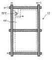
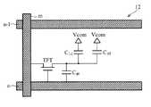
図1及び図2に示すように、従来のカラー液晶ディスプレイ(以下「LCD」という。)パネル1は、通常、赤(R)、緑(G)、及び青(B)の3つの主カラーからなる複数のサブピクセル10を含む。このRGBの3色成分は、対応するカラーフィルターを用いて実現することができる。図2は、従来のLCDパネルの画素構造の平面図である。図2に示すように、1つの画素は、3つのサブピクセル12R、12G、12Bに分けることができる。図3は、一般の透過型LCDのサブピクセルの構造を表している。図3に示すように、サブピクセル12は、カラーフィルター42及び上基板40の上に配置されたITO電極を含む。LCDのサブピクセル12の下部分には、下透過電極64、保護層65、及び素子層62が下基板60に配置される。サブピクセル12は、上電極と下電極の間に配置された液晶層50を更に含む。上電極は、通常コモンラインに接続され、コモンライン上の電圧はVcomで表示される(図5参照)。図4に示すように、下電極は、スイッチング素子、または薄膜トランジスタ(TFT)によってデータラインmに電気的に接続され、かつ、このスイッチング素子、またはTFTは、ゲートライン(n+1)上の信号によって導通される。図5は、サブピクセル12の等価回路を示す。一般的に、サブピクセル12はいくつかのコンデンサと関連している。コンデンサCLCは、サブピクセルの液晶層の電荷容量である。コンデンサCSTは、サブピクセルの中の電荷蓄積コンデンサであり、ゲートライン信号が通過した後の上電極と下電極との間の電位を維持する。コンデンサCgsは、ゲートとソースとの間のコンデンサであり、サブピクセルにおいて、TFTと保護層と複数のコンデンサの1つと関連がある。ゲートライン信号がオンのとき、それがTFTを駆動し、これらのコンデンサを充電し、少なくともゲートライン信号のオフ前に、透過電極64の電位(VPIXEL)をデータラインmにある信号に実質的に等しくさせる。LCDサブピクセルの設計に基づいて、VPIXELは、一般的にフィードスルー電圧降下として知られる量で減少される。従来のLCDパネル(例えば、マルチドメイン垂直配向(MVA)パネル)では、ガンマ曲線の変化により、ディスプレイの色が視野角に伴って大きく変化する。As shown in FIGS. 1 and 2, a conventional color liquid crystal display (hereinafter referred to as “LCD”)
よって、LCDパネルの色に対する視野角の影響を減少する駆動方法及び画素構造を提供することが望まれている。 Accordingly, it would be desirable to provide a driving method and pixel structure that reduces the effect of viewing angle on the color of the LCD panel.
本発明の代表例の透過型液晶ディスプレイ装置(透過型LCD)は画素構造を有する。この画素構造では、サブピクセルの各々が少なくとも第1領域と少なくとも第2領域とに分けられ、各領域が電極ペアを有する。第1領域の電極ペアがTFTによってゲートライン及びデータラインの少なくとも1つに電気的に接続された第1下電極と、第1コモンラインによって第1電圧に電気的に接続された第1上電極とを含む。第2領域の電極ペアは、もう1つのTFTによってゲートラインかつデータラインの少なくとも1つに電気的に接続された第2下電極、及び第2コモンラインによって第2電圧に電気的に接続された第2上電極を含む。第1電圧及び第2電圧のそれぞれがコモン信号と実質的に異なる信号を有する。A transmissive liquid crystal display device (transmissive LCD) as a representative example of the present invention has a pixel structure. In this pixel structure, each sub-pixel is divided into at least a first region and at least a second region, and each region has an electrode pair. A firstlower electrode in which an electrode pair in the first region is electrically connected to at least one of a gate line and a data line by a TFT; and afirst upper electrode electrically connected to a first voltage by a first common line Including. The electrode pair of the second region is electrically connected to the second voltage by the second common electrode and the secondlower electrode electrically connected to at least one of the gate line and the data line by another TFT. A secondupper electrode is included. Each of the first voltage and the second voltage has a signal substantially different from the common signal.
一方で、各画素は、第1領域の第1下電極と第1コモンラインとの間に電気的に接続された第1蓄積コンデンサ、及び第2領域の第2下電極と第2コモンラインとの間に電気的に接続された第2蓄積コンデンサを有する。Meanwhile, each pixel includes a first storage capacitor electrically connected between the firstlower electrode and the first common line in the first region, and asecond lower electrode and a second common line in the second region. The second storage capacitor is electrically connected between the two.
他の実施例では、画素が第3領域を有する。そして、第3領域が第3電極ペアを有する。さらに第3電極ペアが、異なるTFTによってゲートライン及びデータラインの少なくとも1つに接続された第3下電極と、第3コモンラインによって第3電圧に接続された第3上電極と、を含む。各領域は第2蓄積コンデンサを有し、それぞれの電極ペアと並列接続される。In another embodiment, the pixel has a third region. The third region has a third electrode pair. Furthermore, the third electrode pair includes athird lower electrode connected to at least one of the gate line and the data line by different TFTs, and athird upper electrode connected to the third voltage by the third common line. Each region has a second storage capacitor and is connected in parallel with the respective electrode pair.
本発明のLCDのサブピクセルとその駆動方法によれば、カラーサブピクセルを2つのサブ領域に分け、各サブ領域が別個のスイッチング素子及び蓄積コンデンサを有し、相補的極性の振幅電圧を用いていることにより異なる画素反転構造を達成することが可能となり、従来のディスプレイの色が視野角に伴って大きく変化する問題を改善することができる。 According to the LCD sub-pixel of the present invention and the driving method thereof, the color sub-pixel is divided into two sub-regions, each sub-region having a separate switching element and storage capacitor, and using an amplitude voltage of complementary polarity. This makes it possible to achieve a different pixel inversion structure, which can improve the problem that the color of the conventional display changes greatly with the viewing angle.
本発明についての目的、特徴、及び長所が一層明確に理解されるよう、以下に実施例を示しつつ、図面を参照しながら詳細に、本発明の好適実施形態を説明する。 In order that the objectives, features, and advantages of the present invention will be more clearly understood, preferred embodiments of the present invention will be described in detail with reference to the accompanying drawings.
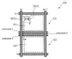
本発明のLCDパネルでは、カラーサブピクセルが2つの領域又は2つ以上の領域に分けることができる。図6に示すように、例えば、カラーサブピクセル120が2つの領域121と領域122とに分けられる。各サブ領域が1つの下電極を有する。図6に示すように、領域121が下電極161を有し、スイッチング素子TFT1を通してデータラインmに電気的に接続される。領域122が下電極162を有し、もう1つのスイッチング素子TFT2を通してデータラインmに電気的に接続される。スイッチング素子TFT1及びTFT2は、ゲートライン(n−1)上の信号により導通される。また、サブピクセル120が2つのコモンラインcommon1及びcommon2と互いに関わり、コモンラインcommon1及びcommon2が上電極141及び電極142(図8参照)のそれぞれ別個に電圧レベルを与えている(すなわち両電極それぞれに差動電圧(異なる電圧;differential voltage)を与えている。)。サブピクセル120が、もう1つのコモンラインcommon3と選択的に互いに関連する。LCDパネルの表示品質(画質の性能)を改善するために、各カラーサブピクセルが、図7Aに示すように、不透明な材料でできたブラックマトリクス(BM)170を有する。また、図7Bに示すように、サブピクセルは、カラーフィルター172を有する。図7Cに示すように、従来のLCDパネルと比べ、サブピクセルが、2つの上電極141及び上電極142を有する。これらの電極は、コモンラインcommon1及びcommon2にそれぞれ接続される。図8に示すように、ブラックマトリクス170は、上基板140の上に配置することができる。カラーフィルター172と、上電極141及び上電極142は、ブラックマトリクス170の上に配置することができる。カラーサブピクセル140の下部分には、下電極161、下電極162、保護層165、及び素子層164が下基板160上に配置されることができる。 In the LCD panel of the present invention, the color subpixel can be divided into two regions or two or more regions. As shown in FIG. 6, for example, the
また、サブ領域121が電荷蓄積コンデンサCST1及びその他のコンデンサ(例えばコンデンサCgs1)と相関性を有する。同様に、サブ領域122は、電荷蓄積コンデンサCST2及びその他のコンデンサ(例えばコンデンサCgs2)と相関性を有する(相関関係がある)。電荷蓄積コンデンサCST1及びCST2がコモン電圧Vcom(図6のコモンラインcommon3)にそれぞれ接続され、固定電位を有する。図9に示すように、上電極141がコモンラインcommon1に電気的に接続され、上電極142がコモンラインcommon2に電気的に接続される。Also has a correlation with the
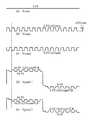
図10の(a)〜図10の(h)は、異なるゲートライン、データライン、及びコモンライン上の信号を表している。図10の(a)は、ゲートライン(n−1)の信号を表しており、図10の(b)は、ゲートラインnの信号を表しており、図10の(c)は、ゲートライン(n+1)の信号を表している。図9に示されるサブピクセル120は、ゲートライン(n−1)によって駆動される。図10の(d)及び図10の(e)は、コモンラインcommon1及びcommon2上の信号を表している。図示されるように、コモンライン上の信号は、好ましくは、周期的な振幅(振動)形式であり、かつ、この2つの信号は互いに同期し、かつ異なる極性を有する。図10の(f)は、データラインmの上の信号を表している。図示されるように、データライン上の信号レベルは異なる値を有する可能性があるが、ゲートラインn−1期間の信号レベルV_signalのみが、サブ領域121の電極上とサブ領域122の電極上の電位を決定する。図10の(g)が、サブ領域121の電極161に用いられる電圧VPIXEL1を表しており、図10の(h)が、サブ領域122の電極162に用いられる電圧VPIXEL2を表している。FIGS. 10A to 10H show signals on different gate lines, data lines, and common lines. 10A shows the signal of the gate line (n−1), FIG. 10B shows the signal of the gate line n, and FIG. 10C shows the gate line. (N + 1) signals are represented. The
サブ領域121の、電極161と電極141との間の1フレーム時間実効(r.m.s.)電位圧VPIXEL1_RMSと、サブ領域122の電極162と電極142との間の1フレーム時間実効(r.m.s.)電位圧VPIXEL2_RMSは、数式(1)と(2)でそれぞれ表される:
この中のCothersは、コンデンサCgs、サブ領域のスイッチング素子、及び保護層、又は素子層と相関する静電容量を含む。注意すべき点は、本発明の実施例は、1*ΔVcomを実施例としているが、これを限定するものではなく、n*ΔVcomとすることもでき、nは、1より大きい、または等しい自然数である。即ち、1.5*ΔVcom、2*ΔVcom、4*ΔVcom、4*ΔVcom、・・・、n*ΔVcom等である点である。One frame time effective (rms) potential voltage VPIXEL1_RMS between the
C others in this includes a capacitorC gs, the switching elements of sub-regions, and the protective layer, or the capacitance correlates with the element layer. It should be noted that although the embodiment of the present invention uses 1* ΔVcom as an example, the present invention is not limited to this, and may be n* ΔVcom, where n is a natural number greater than or equal to 1. It is. That is, 1.5* ΔVcom, 2* ΔVcom, 4* ΔVcom, 4* ΔVcom,..., N* ΔVcom, and the like.
本発明のもう1つの実施例では、同じサブ領域のコンデンサCLC及びCSTが同じコモンラインに接続されるようにされている。図11に示されるように、サブ領域121のコンデンサCLC1及びCST1は、コモンラインcommon1に接続され、かつ、サブ領域122のコンデンサCLC2及びCST2は、コモンラインcommon2に接続される。電位VPIXEL1及びVPIXEL2は、数式(4)及び(5)でそれぞれ表される:
また、第2部分の実効(r.m.s.)値は、(6)で表される:
以上の数式が電荷蓄積容量を含むことから、コモンラインcommon1及びcommon2の接合電圧は、CLC値に対して感受性(sensitivity)が低下する。これは、LCDパネルを製造する上で、より高い製造誤差を許容させる。同時に、ΔVcomの振幅を減少することができる。注意すべき点は、本明細書では、1*ΔVcomを実施例としているが、これに限定されるものではなく、n*ΔVcomとすることもでき(nは自然数)、即ち、1.5*ΔVcom、2*ΔVcom、4*ΔVcom、4*ΔVcom、・・・、n*ΔVcom等とすることができる点である。In another embodiment of the present invention, capacitors CLC and CST in the same sub-region are connected to the same common line. As shown in FIG. 11, the capacitors CLC1 and CST1 in the
The effective (rms) value of the second part is represented by (6):
Since the above formulas includes a charge storage capacitor, the junction voltage of the common line common1 and common2is sensitive (sensitivity) is decreased with respect toC LC value. This allows a higher manufacturing error in manufacturing the LCD panel. At the same time, the amplitude of ΔVcom can be reduced. In this specification, 1* ΔVcom is taken as an example in the present specification, but is not limited thereto, and may be n* ΔVcom (n is a natural number), that is, 1.5* ΔVcom, 2* ΔVcom, 4* ΔVcom, 4* ΔVcom,..., N* ΔVcom, and the like.
本発明の他の実施例では、カラーサブピクセルはまた、3つのサブ領域に分けられることができる。図12に示すように、サブピクセル120’は、上電極141、142、及び143と下電極161、162、及び163で画定された3つのサブ領域121、122、及び123を有する。例えば、上電極141、142、及び143は、コモンラインcommon1、common3、common2にそれぞれ接続される。同様に、図13に示すように、電荷蓄積コンデンサCST1、CST2、CST3は、コモンラインcommon1、common3、common2にそれぞれ接続される。よって、電位VPIXEL1、VPIXEL2、VPIXEL3は、数式(7)〜(9)でそれぞれ表される:
また、数式(7)〜(9)の第2部分の実効(r.m.s.)値は、(10)で表される。
In addition, the effective (r.m.s.) value of the second part of the mathematical formulas (7) to (9) is represented by (10).
図14の(a)〜(j)は、異なるゲートライン、データライン、コモンライン上の信号を表している。図14の(a)は、ゲートライン(n−1)の信号を表しており、図14の(b)は、ゲートラインnの信号を表しており、図14の(c)は、ゲートライン(n+1)の信号を表している。図14の(d)は、上電極141及び電荷蓄積コンデンサCST1に提供されたコモンラインcommon1上の信号を表しており、図14の(e)は、上電極143及び電荷蓄積コンデンサCST3に提供されたコモンラインcommon2上の信号を表しており、図14の(f)は、上電極142と電荷蓄積コンデンサCST2に提供されたコモンラインcommon3上の信号を表している。図示されるように、コモンラインcommon1及びcommon2の信号では、好ましくは、実質的に交番態様の2つの電位を有する。コモンラインcommon3の信号では、好ましくは固定電圧を有するが、これを限定するものでなく、実質的に変動可能な電圧とすることができる。図14の(g)は、データラインm上の信号を表している。図14の(h)は、サブ領域121の電極161に用いられる電圧VPIXEL1を表しており、図14の(i)は、サブ領域122の電極162に用いられる電圧VPIXEL2を表しており、図14の(j)は、サブ領域123の電極163に用いられる電圧VPIXEL3を表している。注意しなければならないのは、本発明の実施例は、1*ΔVcomを実施例に適用しているが、これを限定するものではなく、n*ΔVcomとすることもでき、nは、1より大きい、または等しい自然数である点である。即ち、1.5*ΔVcom、2*ΔVcom、4*ΔVcom、4*ΔVcom、...、n*ΔVcomなどである。14A to 14J show signals on different gate lines, data lines, and common lines. 14A shows the signal of the gate line (n−1), FIG. 14B shows the signal of the gate line n, and FIG. 14C shows the gate line. (N + 1) signals are represented. FIG. 14 (d) represents the signal on common line common1 provided above the
本発明のもう1つの実施例では、カラーサブピクセルはまた、図15に示すように、3つのサブ領域121、122、及び123に分けられることができる。サブ領域121、122、及び123は、下電極161、162、及び163で画定される。しかし、2つの上電極141及び上電極142のみ有する。ここでは、サブピクセル120と相関する4つのコンデンサを有する。コンデンサCST1が下電極161と相関し、コンデンサCST1−2が下電極162と相関し、コンデンサCST2−3が下電極162と相関し、かつ、コンデンサCST3は、下電極163と相関する。例えば、仮に、コンデンサCST1及びCST1−2をコモンラインcommon1にそれぞれ接続させ、かつ、コンデンサCST2−3及びCST13をコモンラインcommon2にそれぞれ接続させた場合、サブ領域121、122、123と相関した電位VPIXEL1、VPIXEL2、VPIXEL3は、数式(11)〜(13)でそれぞれ表される:
数式(12)では、CLC1−2及びCLC2−3は、サブ領域122の液晶層と相関する静電容量である。仮に、サブ領域の設計をCLC1−2=CLC2−3、かつ、
CST1−2=CST2−3にした場合、数式(12)は:
に簡略化することができる。
また、数式(11)〜(13)の第2部分の実効(r.m.s.)値は、(14)で表される:
In Expression (12), CLC1-2 and CLC2-3 are capacitances correlated with the liquid crystal layer in the
When CST1-2 = CST2-3 , formula (12) is:
Can be simplified.
In addition, the effective (r.m.s.) value of the second part of the formulas (11) to (13) is represented by (14):
ここで注意すべき点は、図15の実施例では、3つのサブ領域の駆動波形が実質的に図12の実施例の駆動波形と同じ点にある。図15の実施例で付加された利点は、2つのコモンラインcommon1とcommon2の使用のみを必要とする点である。図12の下電極162のように、図15の下電極162もゲートライン信号(図13参照)によって駆動されたスイッチング素子TFT2を通してデータラインに接続される。さらに注意すべき点は、本発明の実施例は、1*ΔVcomを実施例としているが、これを限定するものではなく、n*ΔVcomとすることもでき、nは、1より大きい又は等しい自然数である。即ち、1.5*ΔVcom、2*ΔVcom、4*ΔVcom、4*ΔVcom、・・・、n*ΔVcom等である点にある。It should be noted that in the embodiment of FIG. 15, the driving waveforms of the three sub-regions are substantially the same as the driving waveforms of the embodiment of FIG. An advantage added in the embodiment of FIG. 15 is that it requires only the use of two common lines common1 and common2. Like the
図10及び図14では、コモンラインcommon1及びcommon2の信号レベルが、振幅周期又は期間(各2つのゲートライン信号と実質的に等しい)内で変更され、それは実質的に2倍または3倍以上の振幅周期であることもできる。図16に示すように、実質的に2倍となった振幅周期が、その振幅周期を4つのゲートライン信号に実質的に等しくさせる。図16の(a)は、ゲートライン(n−1)の信号を表しており、図16の(b)は、ゲートラインnの信号を表しており、図16の(c)は、ゲートライン(n+1)の信号を表している。図16の(d)と図16の(e)は、コモンラインcommon1及びcommon2の信号をそれぞれ表している。図16の(f)は、データラインm上の信号を表している。図16の(g)は、サブ領域121の電極161の電圧VPIXEL1を表しており、図16の(h)は、サブ領域122の電極162の電圧VPIXEL2を表している。10 and 14, the signal levels of common lines common1 and common2 are changed within an amplitude period or period (substantially equal to each two gate line signals), which is substantially two times or more than three times. It can also be an amplitude period. As shown in FIG. 16, the amplitude period substantially doubled causes the amplitude period to be substantially equal to the four gate line signals. 16A shows the signal of the gate line (n−1), FIG. 16B shows the signal of the gate line n, and FIG. 16C shows the gate line. (N + 1) signals are represented. (D) in FIG. 16 and (e) in FIG. 16 represent signals of the common lines common1 and common2, respectively. FIG. 16F shows a signal on the data line m. FIG.16G shows the voltage VPIXEL1 of the
以上をまとめると、本発明のLCDパネルでは、サブピクセルは、少なくとも2つのサブ領域に分けられ、各サブ領域は、別個の電極ペアを有し、差動電圧により、1つのサブ領域の液晶層全体の電位をもう1つのサブ領域と実質的に異ならせる。特に、各サブ領域が別個の上電極と別個の下電極を有するとき、異なるサブ領域の下電極は、好ましくは、同じデータラインにそれぞれ接続されるが、これを限定するものではない。また、異なるサブ領域の上電極は、異なるコモンラインに接続され、好ましくは、前記異なるコモンラインの電気的性質は、実質的に互いに異なるが、これを限定するものではない。また、各サブ領域は、別個の電荷蓄積コンデンサを有する。異なるサブ領域の電荷蓄積コンデンサは、電気的性質が実質的に同じ電圧、または電気的性質が実質的に異なるコモンラインに接続されることができる。コモンラインcommon1及びcommon2の信号では、好ましくは、2つの信号レベル間で交番するが、極性が実質的に異なる実質的に同じ振幅波形を有する。よって、1つのサブ領域の輝度が実質的に低下したとき、もう1つのサブ領域の輝度が実質的に上昇する。 In summary, in the LCD panel of the present invention, the sub-pixel is divided into at least two sub-regions, each sub-region has a separate electrode pair, and the liquid crystal layer of one sub-region is formed by a differential voltage. The overall potential is made substantially different from the other subregion. In particular, when each sub-region has a separate upper electrode and a separate lower electrode, the lower electrodes of the different sub-regions are preferably connected to the same data line, respectively, but this is not a limitation. Further, the upper electrodes of different sub-regions are connected to different common lines. Preferably, the electrical properties of the different common lines are substantially different from each other, but the present invention is not limited thereto. Each subregion also has a separate charge storage capacitor. The charge storage capacitors in different sub-regions can be connected to voltages having substantially the same electrical properties or common lines having substantially different electrical properties. The signals of common lines common1 and common2 preferably have substantially the same amplitude waveform alternating between the two signal levels, but with substantially different polarities. Therefore, when the luminance of one sub-region is substantially reduced, the luminance of the other sub-region is substantially increased.
正フレーム及び負フレームの適当な振幅電圧波形がLCDパネルの画素のサブ領域に別個に提供されたとき、異なる画素反転の効果を達成することができる。図17の(d)及び図17の(e)は、カラーサブピクセル120のサブ領域121及び122に別個に提供された波形を表しており、図17では、2*ΔVcomを実施例としてそれぞれ説明しているが、これを限定するものではなく、その他の倍率のΔVcomとすることもできる。図17の(d)に示される波形は、図16の(h)の波形に実質的に似ているが、2つのフレーム時間に延伸される。同様に、図17の(e)に示される波形は、図16の(g)の波形に実質的に似ているが、2つのフレーム時間に実質的に延伸される。仮に、図17の(a)に示されるように、固定のVcom信号を略5.5Vにした場合、Vcom1またはサブ領域121の振幅電圧と、Vcom2又はサブ領域121は、図17の(b)及び図17の(c)に示すように、実質的にn*ΔVcomに5.5Vプラス又は5.5Vマイナスとなる。また、図17では、1*ΔVcom及び2*ΔVcomを実施例として説明しているが、これを限定するものではない。また、Vcom1及びVcom2の信号は極性においてのみ実質的に異なる。仮に、V_signalを正フレームで略10.5Vにし、負フレームで略0.5Vにした場合、正フレーム期間内では、VPIXEL1は、約(10.5V+2ΔVcom×結合率(カップリング比(couplung ratio);CR))と約10.5Vの間で交番し、VPIXEL2は、約10.5Vと約(10.5V−2ΔVcom×CR)の間で交番する。負フレーム期間内では、VPIXEL1は、約0.5Vと約(0.5V−2ΔVcom×CR)の間で交番し、VPIXEL2は、約(0.5V+2ΔVcom×CR)と約0.5Vの間で交番する。ここでは、サブ領域121の結合率CRに関しては、CLC1/(CLC1+CST+Cothers)であり、サブ領域122の結合率CRに関しては、CLC2/(CLC2+CST+Cothers)(数式1と数式2)である。Different pixel inversion effects can be achieved when appropriate amplitude voltage waveforms for the positive and negative frames are provided separately to the pixel sub-regions of the LCD panel. FIGS. 17D and 17E show waveforms separately provided in the
図18Aと図18Bは、正フレームと負フレーム期間内の画素の概略図を表している。上向きに指している矢印は、各カラーピクセルR、Gと、Bのサブ領域121のプルアップのV_signalを示しており、下向きに指している矢印は、各カラーピクセルR、Gと、Bのサブ領域122のプルダウンのV_signalを示している。文字“H”は、印加された電圧が実質的に比較的高いことからサブ領域がより明るいことを示している。同様に、文字“L”は、印加された電圧が実質的に比較的低いことからサブ領域がより暗いことを示している。図19Aに示すように、波形VPIXEL1とVPIXEL2をLCDパネルの複数の画素に供給し、ドット反転構造を達成することが可能である。図19Bと図19Cに示すように、実質的に類似の波形を供給してツーライン(2行)(two−line)反転構造とカラム反転を達成することも可能である。18A and 18B show schematic diagrams of pixels in the positive frame and negative frame periods. The arrow pointing upward indicates the V_signal of the pull-up of each color pixel R, G, and
よって、カラーサブピクセルを2つのサブ領域に分け、各サブ領域が別個のスイッチング素子と蓄積コンデンサを有することで、相補的極性の振幅電圧を用いて異なる画素反転構造を達成することが可能である。 Thus, it is possible to achieve different pixel inversion structures using complementary polarity amplitude voltages by dividing the color sub-pixel into two sub-regions, each sub-region having a separate switching element and storage capacitor. .
注意すべき点は、本発明の実施例で述べた、2つのコモンライン上の信号が、周期性の振幅(振動)形式であることである。この2つの信号は互いに同期するため実質的に異なる極性を実施例としているがこれを限定するものではなく、その他の型式を用いることもできる。例えば、2つの信号が実質的に同じ極性で同期する、2つの信号が実質的に異なる極性で同期しない、又は、2つの信号が実質的に同じ極性だが同期しない、又は、その他の型式、または上述の組み合わせの型式を用いることもできる。また、仮に、第3のコモンラインも存在するとき、第3のコモンライン上の信号が、2つのコモンライン上の信号に選択的に合わせて変えられる。例えば、数値、極性、その他、若しくは上述の組み合わせに合わせて変えられる。換言すると、第3コモンライン上の信号が、実質的に前記第1コモンライン上の信号及び前記第2コモンライン上の信号の少なくとも1つと異なるようにする。また、仮に第3コモンライン上の信号値が、本発明の上述の実施例で述べた第1と第2コモンライン上の信号の実効値(r.m.s.)以外の場合でも、例えば、第1と第2コモンライン上の信号の平均値とすることができ、またはその他の方法、または上述の組み合わせであることもできる。また、本発明の上述の実施例で述べたサブピクセルで分けられた複数のサブ領域は、各領域が電極ペアを有する。前記領域のその中の1つの電極ペアは、電極を含み、1つのTFTによってゲートラインとデータラインの少なくとも1つに電気的に接続される。前記領域のその中のもう1つの電極ペアは、電極を含み、もう1つのTFTによってゲートラインとデータラインの少なくとも1つに電気的に接続され、異なる領域の中の電極で、異なるTFTによって同じ電極ライン及びデータラインに電気的に接続されるのを実施例としているが、これも、このことを限定するものではない。即ち、本発明の上述の実施例で述べた、異なるTFTによってゲートライン及びデータラインの少なくとも1つに電気的に接続された異なる領域の中の電極が異なる。 It should be noted that the signals on the two common lines described in the embodiments of the present invention are in the form of periodic amplitude (vibration). Since these two signals are synchronized with each other, substantially different polarities are taken as an example, but this is not a limitation, and other types can be used. For example, two signals are synchronized with substantially the same polarity, two signals are not synchronized with substantially different polarity, or two signals are substantially the same polarity but not synchronized, or other types, or The combination type described above can also be used. If the third common line is also present, the signal on the third common line is selectively changed to the signal on the two common lines. For example, it can be changed in accordance with a numerical value, polarity, other, or a combination described above. In other words, the signal on the third common line is substantially different from at least one of the signal on the first common line and the signal on the second common line. Even if the signal value on the third common line is other than the effective value (rms) of the signal on the first and second common lines described in the above embodiment of the present invention, for example, , The average value of the signals on the first and second common lines, or other methods or combinations of the above. In addition, each of the plurality of sub-regions divided by the sub-pixels described in the above embodiment of the present invention has an electrode pair. One electrode pair in the region includes electrodes and is electrically connected to at least one of the gate line and the data line by one TFT. Another electrode pair in the region includes an electrode and is electrically connected to at least one of the gate line and the data line by another TFT, and the electrode in a different region is the same by a different TFT. Although the embodiment is described as being electrically connected to the electrode line and the data line, this is not limited thereto. That is, the electrodes in the different regions electrically connected to at least one of the gate line and the data line by different TFTs as described in the above embodiments of the present invention are different.
また、本発明は、透過型LCDパネルと連結した形態を実施例として説明しているが、本発明は、半透過型LCDパネル、または反射型LCDパネルを用いることもできる。 Further, although the present invention has been described by way of an embodiment in which a transmissive LCD panel is connected, a transflective LCD panel or a reflective LCD panel can also be used in the present invention.
以上、本発明の好適な実施例を例示したが、これは本発明を限定するものではなく、本発明の精神及び範囲を逸脱しない限りにおいては、当業者であれば行い得る少々の変更や修飾を付加することは可能である。従って、本発明が保護を請求する範囲は、特許請求の範囲を基準とする。 The preferred embodiments of the present invention have been described above, but this does not limit the present invention, and a few changes and modifications that can be made by those skilled in the art without departing from the spirit and scope of the present invention. It is possible to add. Accordingly, the scope of the protection claimed by the present invention is based on the scope of the claims.
1 液晶表示装置
10 画素
12、12R、12G、12B サブピクセル
40、140 上基板
42 カラーフィルター
44 ITO電極
50 液晶層
60、160 下基板
62、164 素子層
64 下透過電極
65、165 保護層
120、120’、120” サブピクセル
121、122、123 サブ領域
161、162、163 下電極
141、142、143上電極
170 ブラックマトリクス
172 カラーフィルター
DESCRIPTION OF
Claims (14)
Translated fromJapanese当該複数のサブピクセルは、少なくとも第1領域及び第2領域に分かれ、ゲートライン及びデータラインにより、複数の画素を画定する液晶層を持つ液晶ディスプレイ装置の画像の性能を向上させる方法であって、
前記サブピクセルの前記第1領域における前記液晶層を挟んで互いに対向する電極である第1電極ペアは、前記ゲートライン上の信号によって駆動される第1スイッチング素子を介して前記データラインに電気的に接続された第1下電極と、第1コモンラインに電気的に接続された第1上電極と、を備え、
前記サブピクセルの前記第2領域における前記液晶層を挟んで互いに対向する電極である第2電極ペアは、前記ゲートライン上の信号によって駆動される第2スイッチング素子を介して前記データラインに電気的に接続された第2下電極と、第2コモンラインに電気的に接続された第2上電極と、を備え、
前記第1コモンラインに第1電圧を印加し、
前記第2コモンラインに第2電圧を印加し、
前記第2電圧と前記第1電圧は、第1値と第2値との間で互いに位相が異なる交番する波形であることを特徴とする液晶ディスプレイ装置の画像の性能を向上させる方法。At least some of the plurality of pixels include a plurality of sub-pixels;
The plurality of subpixelsare divided into at least a first region and a second region,and a method for improving image performance of a liquid crystal display device having a liquid crystal layer defining a plurality of pixels by gate linesand data lines,
A first electrode pair that is an electrode facing each other across the liquid crystal layer in the first region of the sub-pixel is electrically connected to the data line via a first switching element driven by a signal on the gate line. A first lower electrode connected to the first common electrode, and a first upper electrode electrically connected to the first common line,
A second electrode pair that is an electrode facing each other across the liquid crystal layer in the second region of the subpixel is electrically connected to the data line via a second switching element driven by a signal on the gate line. A second lower electrode connected to the second common electrode, anda second upper electrode electrically connected to the second common line,
Applying a first voltage to the first common line;
Applying a second voltage to the second common line;
The method of improving image performance of a liquid crystal display device, wherein the second voltage and the first voltage are alternating waveforms having different phases between the first value and the second value.
前記第3コモンラインに第3電圧を印加し、その結果、該第3電圧を、前記第1電圧及び前記第2電圧の少なくともいずれかと異ならせるステップを更に含む請求項1に記載の液晶ディスプレイ装置の画像の性能を向上させる方法。Each region of the sub-pixel has a storage capacitor connected to a third common line;
The liquid crystal display device according to claim 1, further comprising: applying a third voltage to the third common line, and as a result, making the third voltage different from at least one of the first voltage and the second voltage. To improve image performance.
前記第1画素コンデンサ及び前記第1蓄積コンデンサが、前記第1領域の前記第1下電極と前記第1コモンラインとの間に電気的に接続され、及び、前記第2画素コンデンサ及び前記第2蓄積コンデンサが、前記第2領域の前記第2下電極と前記第2コモンラインとの間に電気的に接続されている請求項1に記載の液晶ディスプレイ装置の画像の性能を向上させる方法。The sub-pixel includes a first pixel capacitor, a first storage capacitor, a second pixel capacitor, and a second storage capacitor;
The first pixel capacitor and the first storage capacitor are electrically connected between the first lower electrode and the first common line in the first region, and the second pixel capacitor and the second storage capacitor. The method according to claim 1, wherein a storage capacitor is electrically connected between the second lower electrode and the second common line in the second region.
前記サブピクセルのそれぞれの前記第3領域で第3電極ペアを、前記液晶層の前記第1側及び第2側のそれぞれに対向する側に配置し、
前記第3電極ペアが前記ゲートライン上の信号によって駆動される第3スイッチング素子によって、前記データラインに電気的に接続された第3下電極及び第3コモンラインに電気的に接続された第3上電極を含み、
前記第3コモンラインに第3電圧を印加し、その結果、前記第3電圧を、前記第1電圧及び第2電圧の少なくとも1つと異ならせることを更に含む請求項1に記載の液晶ディスプレイ装置の画像の性能を向上させる方法。The sub-pixel further includes a third region;
A third electrode pair in each of the third regions of the sub-pixels is disposed on a side of the liquid crystal layer facing the first side and the second side;
The third electrode pair is electrically connected to a third lower electrode and a third common line electrically connected to the data line by a third switching element driven by a signal on the gate line. Including an upper electrode,
2. The liquid crystal display device according to claim 1, further comprising applying a third voltage to the third common line so that the third voltage is different from at least one of the first voltage and the second voltage. A way to improve image performance.
前記第1領域の前記第1下電極と前記第1コモンラインとの間に電気的に接続された第1画素コンデンサ及び第1蓄積コンデンサと、
前記第2領域の前記第2下電極と前記第2コモンラインとの間に電気的に接続された第2画素コンデンサ及び第2蓄積コンデンサと、
前記第3領域の前記第3下電極と前記第3コモンラインとの間に電気的に接続された第3画素コンデンサと第3蓄積コンデンサと、を含む請求項5に記載の液晶ディスプレイ装置の画像の性能を向上させる方法。The subpixel is
A first pixel capacitor and a first storage capacitor electrically connected between the first lower electrode of the first region and the first common line;
A second pixel capacitor and a second storage capacitor electrically connected between the second lower electrode of the second region and the second common line;
The image of the liquid crystal display device according to claim 5, further comprising: a third pixel capacitor and a third storage capacitor electrically connected between the third lower electrode and the third common line in the third region. To improve performance.
前記ゲートラインの信号によって駆動される第3スイッチング素子を介して、前記第3電極を前記データラインに電気的に接続する請求項1に記載の液晶ディスプレイ装置の画像の性能を向上させる方法。A third lower electrode is disposed between the first lower electrode of the first electrode pair and the second lower electrode of the second electrode pair;
The method according to claim 1, wherein the third electrode is electrically connected to the data line through a third switching element driven by a signal of the gate line.
前記第1領域と前記第2領域との間に配置された、前記第1領域に隣接する第3領域と、前記第2領域に隣接する第4領域と、
前記第1領域の前記第1下電極と前記第1コモンラインとの間に電気的に接続された第1画素コンデンサ及び第1蓄積コンデンサと、
前記第2領域の前記第2下電極と前記第2コモンラインとの間に電気的に接続された第2画素コンデンサ及び第2蓄積コンデンサと、
前記第3領域の前記第3下電極と前記第1コモンラインとの間に電気的に接続された第3蓄積コンデンサと、
前記第4領域の前記第3下電極と前記第2コモンラインとの間に電気的に接続された第4蓄積コンデンサと、を含む請求項7に記載の液晶ディスプレイ装置の画像の性能を向上させる方法。The subpixel is
A third region adjacent to the first region, a fourth region adjacent to the second region, disposed between the first region and the second region;
A first pixel capacitor and a first storage capacitor electrically connected between the first lower electrode of the first region and the first common line;
A second pixel capacitor and a second storage capacitor electrically connected between the second lower electrode of the second region and the second common line;
A third storage capacitor electrically connected between the third lower electrode of the third region and the first common line;
The liquid crystal display device according to claim 7, further comprising a fourth storage capacitor electrically connected between the third lower electrode of the fourth region and the second common line. Method.
前記サブピクセルの前記第1領域における前記液晶層を挟んで互いに対向する電極である第1電極ペアであって、前記ゲートライン上の信号によって駆動される第1スイッチング素子を介して前記データラインに電気的に接続された第1下電極と、第1コモンラインに電気的に接続された第1上電極と、を含む前記第1電極ペアと、
前記サブピクセルの前記第2領域における前記液晶層を挟んで互いに対向する電極である第2電極ペアであって、前記ゲートライン上の信号によって駆動される第2スイッチング素子を介して前記データラインに電気的に接続された第2下電極と、第2コモンラインに電気的に接続された第2上電極と、を含む前記第2電極ペアと、
を備え、
前記第1コモンラインが第1電圧と接続され、
前記第2コモンラインが第2電圧と接続され、
前記第1電圧と前記第2電圧とは、第1値と第2値の間で互いに位相が異なる交番する波形であることを特徴とする液晶ディスプレイパネル。At least some of the plurality of pixels includes a plurality of sub-pixels, the plurality of sub-pixels, defines at least a first region isdivided into a second region, a plurality of pixels by the gate lines and the data lines A liquid crystal display panel having a liquid crystal layer,
A first electrode pair which is an electrode opposed to each other across the liquid crystal layer in the first region of the sub-pixel, and is connected to the data line via a first switching element driven by a signal on the gate line. The first electrode pair comprising: a first lower electrode electrically connected; and a first upper electrode electrically connected to a first common line;
A second electrode pair which is an electrode facing each other across the liquid crystal layer in the second region of the subpixel, and is connected to the data line via a second switching element driven by a signal on the gate line. The second electrode pair comprising: a second lower electrode electrically connected; and a second upper electrode electrically connected to a second common line;
With
The first common line is connected to a first voltage;
The second common line is connected to a second voltage;
The liquid crystal display panel according to claim 1, wherein the first voltage and the second voltage are alternating waveforms having different phases between the first value and the second value.
前記第1領域の前記第1下電極と前記第1コモンラインとの間に電気的に接続された第1画素コンデンサ及び第1蓄積コンデンサと、
前記第2領域の前記第2下電極と前記第2コモンラインとの間に電気的に接続された第2画素コンデンサ及び第2蓄積コンデンサと、を更に含む請求項9に記載の液晶ディスプレイパネル。Each of the sub-pixels is
A first pixel capacitor and a first storage capacitor electrically connected between the first lower electrode of the first region and the first common line;
10. The liquid crystal display panel according to claim 9, further comprising a second pixel capacitor and a second storage capacitor electrically connected between the second lower electrode of the second region and the second common line.
前記サブピクセルの各々が、前記サブピクセルの各々の前記第2領域の前記液晶層の互いに対向する第1及び第2の側に配置され、第3スイッチング素子によって、前記データラインに電気的に接続された第3下電極及び第3コモンラインに電気的に接続された第3上電極を含み、
前記第3コモンラインが第3電圧に電気的に接続され、かつ、前記第3電圧が前記第1電圧及び第2電圧の少なくとも1つと異なる第3電極ペアを更に含む請求項9に記載の液晶ディスプレイパネル。The sub-pixel is divided into the first region, the second region, and the third region;
Each of the sub-pixels is disposed on the first and second sides of the liquid crystal layer facing each other in the second region of each of the sub-pixels, and is electrically connected to the data line by a third switching element. A third upper electrode electrically connected to the third lower electrode and the third common line,
The liquid crystal according to claim 9, further comprising a third electrode pair in which the third common line is electrically connected to a third voltage, and the third voltage is different from at least one of the first voltage and the second voltage. Display panel.
前記第1領域の前記第1下電極と前記第1コモンラインとの間に電気的に接続された第1画素コンデンサ及び第1蓄積コンデンサと、
前記第2領域の前記第2下電極と前記第2コモンラインとの間に電気的に接続された第2画素コンデンサ及び第2蓄積コンデンサと、
前記第3領域の前記第3下電極と前記第3コモンラインとの間に電気的に接続された第3画素コンデンサ及び第3蓄積コンデンサと、
を更に含む請求項13に記載の液晶ディスプレイパネル。Each of the sub-pixels is
A first pixel capacitor and a first storage capacitor electrically connected between the first lower electrode of the first region and the first common line;
A second pixel capacitor and a second storage capacitor electrically connected between the second lower electrode of the second region and the second common line;
A third pixel capacitor and a third storage capacitor electrically connected between the third lower electrode of the third region and the third common line;
The liquid crystal display panel according to claim 13, further comprising:
Applications Claiming Priority (2)
| Application Number | Priority Date | Filing Date | Title |
|---|---|---|---|
| US11/405,974US7589703B2 (en) | 2006-04-17 | 2006-04-17 | Liquid crystal display with sub-pixel structure |
| US11/405,974 | 2006-04-17 |
Publications (2)
| Publication Number | Publication Date |
|---|---|
| JP2007286624A JP2007286624A (en) | 2007-11-01 |
| JP5026847B2true JP5026847B2 (en) | 2012-09-19 |
Family
ID=38604384
Family Applications (1)
| Application Number | Title | Priority Date | Filing Date |
|---|---|---|---|
| JP2007108273AActiveJP5026847B2 (en) | 2006-04-17 | 2007-04-17 | Method for improving image performance of liquid crystal display device and liquid crystal display panel |
Country Status (4)
| Country | Link |
|---|---|
| US (1) | US7589703B2 (en) |
| JP (1) | JP5026847B2 (en) |
| CN (1) | CN100465744C (en) |
| TW (1) | TWI336872B (en) |
Families Citing this family (29)
| Publication number | Priority date | Publication date | Assignee | Title |
|---|---|---|---|---|
| US8107030B2 (en)* | 2005-09-15 | 2012-01-31 | Haip L. Ong | Pixels using associated dot polarity for multi-domain vertical alignment liquid crystal displays |
| WO2008018552A1 (en)* | 2006-08-10 | 2008-02-14 | Sharp Kabushiki Kaisha | Liquid crystal display |
| TWI345748B (en)* | 2006-09-05 | 2011-07-21 | Chunghwa Picture Tubes Ltd | Thin film transistor liquid crystal display |
| TWI356222B (en)* | 2006-09-18 | 2012-01-11 | Chimei Innolux Corp | Liquid crystal display panel and liquid crystal di |
| TWI358050B (en)* | 2007-01-24 | 2012-02-11 | Au Optronics Corp | Pixel structure and method for generating drive vo |
| TWI372929B (en)* | 2007-03-30 | 2012-09-21 | Chunghwa Picture Tubes Ltd | Pixel structure and driving method |
| TWI363912B (en)* | 2007-06-20 | 2012-05-11 | Au Optronics Corp | Display panel and fabricating method thereof, electro-optical device comprising said display panel, and fabricating method thereof |
| KR101487738B1 (en)* | 2007-07-13 | 2015-01-29 | 삼성디스플레이 주식회사 | Liquid crystal display and method of driving thereof |
| CN101809492B (en)* | 2007-11-29 | 2012-09-19 | 夏普株式会社 | Display device and driving method of display device |
| TWI362528B (en) | 2008-01-02 | 2012-04-21 | Au Optronics Corp | Pixel structure and liquid crystal display having the same |
| CN101221332B (en)* | 2008-01-17 | 2010-06-23 | 友达光电股份有限公司 | Pixel structure and LCD with the same |
| JP5486850B2 (en)* | 2008-06-20 | 2014-05-07 | 三星ディスプレイ株式會社 | Display panel, liquid crystal display device including the same, and manufacturing method thereof |
| TWI404024B (en)* | 2008-06-30 | 2013-08-01 | Innolux Corp | Driving methods of pixel set, flat display panel and flat panel display apparatus |
| KR101549962B1 (en)* | 2008-11-28 | 2015-09-04 | 삼성디스플레이 주식회사 | Liquid crystal display |
| TWI386743B (en)* | 2009-12-01 | 2013-02-21 | Au Optronics Corp | Display panel |
| KR20120056110A (en)* | 2010-11-24 | 2012-06-01 | 삼성모바일디스플레이주식회사 | Liquid crystal display and inversion driving method |
| US8564628B2 (en) | 2011-01-26 | 2013-10-22 | Nokia Corporation | Display apparatus |
| TWI559047B (en)* | 2012-06-13 | 2016-11-21 | 友達光電股份有限公司 | Pixel array substrate, liquid crystal display and method of manufacturing liquid crystal display |
| KR101961145B1 (en) | 2012-10-17 | 2019-03-26 | 삼성디스플레이 주식회사 | Display apparatus |
| TWI486928B (en)* | 2012-11-16 | 2015-06-01 | Au Optronics Corp | Display and detecting method thereof |
| CN103513484B (en)* | 2013-06-19 | 2017-03-01 | 深圳市华星光电技术有限公司 | Liquid crystal array substrate and liquid crystal array substrate method of testing |
| JP6214767B2 (en)* | 2013-10-21 | 2017-10-18 | ビーイー・エアロスペース・インコーポレーテッドB/E Aerospace, Inc. | Independently articulating seat pan for aircraft seats |
| CN104076565A (en)* | 2014-06-11 | 2014-10-01 | 深圳市华星光电技术有限公司 | Array substrate and display device |
| US10288953B2 (en) | 2016-10-18 | 2019-05-14 | Shenzhen China Star Optoelectronics Technology Co., Ltd. | Pixel structure and liquid crystal display panel |
| CN106249498B (en)* | 2016-10-18 | 2019-07-16 | 深圳市华星光电技术有限公司 | A kind of dot structure and liquid crystal display panel |
| TWI662327B (en)* | 2018-02-09 | 2019-06-11 | 友達光電股份有限公司 | Display panel |
| CN109143703B (en)* | 2018-09-07 | 2022-03-04 | 上海中航光电子有限公司 | Display panel and 3D printing device |
| CN110136625A (en)* | 2019-05-17 | 2019-08-16 | 京东方科技集团股份有限公司 | Display panel and display device |
| CN117457658A (en)* | 2022-12-31 | 2024-01-26 | Tcl华星光电技术有限公司 | Array substrate and display panel |
Family Cites Families (23)
| Publication number | Priority date | Publication date | Assignee | Title |
|---|---|---|---|---|
| US4775861A (en) | 1984-11-02 | 1988-10-04 | Nec Corporation | Driving circuit of a liquid crystal display panel which equivalently reduces picture defects |
| JP2514731B2 (en) | 1990-02-05 | 1996-07-10 | シャープ株式会社 | Active matrix display |
| JP3029489B2 (en) | 1991-07-25 | 2000-04-04 | キヤノン株式会社 | Display device |
| US5260818A (en) | 1992-05-11 | 1993-11-09 | Industrial Technology Research Institute | Display panel provided with repair capability of defective elements |
| JPH07152013A (en)* | 1993-11-29 | 1995-06-16 | Nippondenso Co Ltd | Liquid crystal display element |
| US6819309B1 (en)* | 1999-07-07 | 2004-11-16 | Canon Kabushiki Kaisha | Double-face display device |
| KR100390456B1 (en)* | 2000-12-13 | 2003-07-07 | 엘지.필립스 엘시디 주식회사 | Liquid crystal display panel and method for manufacturing the same |
| JP4757393B2 (en) | 2001-03-23 | 2011-08-24 | Nec液晶テクノロジー株式会社 | Liquid crystal display device and manufacturing method thereof |
| KR100401377B1 (en)* | 2001-07-09 | 2003-10-17 | 엘지.필립스 엘시디 주식회사 | Liquid Crystal Display Device and Driving Method for the same |
| JP3895952B2 (en)* | 2001-08-06 | 2007-03-22 | 日本電気株式会社 | Transflective liquid crystal display device and manufacturing method thereof |
| JP4111785B2 (en)* | 2001-09-18 | 2008-07-02 | シャープ株式会社 | Liquid crystal display |
| JP2003131636A (en) | 2001-10-30 | 2003-05-09 | Hitachi Ltd | Liquid crystal display |
| JP4019697B2 (en) | 2001-11-15 | 2007-12-12 | 株式会社日立製作所 | Liquid crystal display |
| US6862052B2 (en) | 2001-12-14 | 2005-03-01 | Samsung Electronics Co., Ltd. | Liquid crystal display, thin film transistor array panel for liquid crystal display and manufacturing method thereof |
| JP4342200B2 (en)* | 2002-06-06 | 2009-10-14 | シャープ株式会社 | Liquid crystal display |
| CN1176397C (en)* | 2002-07-15 | 2004-11-17 | 统宝光电股份有限公司 | Liquid crystal display device with a light guide plate |
| CN1209661C (en)* | 2002-08-02 | 2005-07-06 | Nec液晶技术株式会社 | Thin film transistor style LCD with color filter for reducing spot defects |
| JP2004279904A (en) | 2003-03-18 | 2004-10-07 | Fujitsu Display Technologies Corp | Liquid crystal display device and method of manufacturing the same |
| KR20040105934A (en) | 2003-06-10 | 2004-12-17 | 삼성전자주식회사 | Liquid crystal display having multi domain and panel for the same |
| KR101157223B1 (en)* | 2003-10-29 | 2012-06-15 | 엘지디스플레이 주식회사 | In plane switching mode liquid crystal display device and fabrication method threrof |
| JP4265788B2 (en) | 2003-12-05 | 2009-05-20 | シャープ株式会社 | Liquid crystal display |
| KR101121211B1 (en) | 2004-02-17 | 2012-03-23 | 치 메이 옵토일렉트로닉스 코포레이션 | Liquid crystal display device, color filter substrate and protruding structure, and manufacturing method thereof |
| JP4467334B2 (en)* | 2004-03-04 | 2010-05-26 | シャープ株式会社 | Liquid crystal display |
- 2006
- 2006-04-17USUS11/405,974patent/US7589703B2/enactiveActive
- 2007
- 2007-02-13TWTW096105264Apatent/TWI336872B/enactive
- 2007-03-09CNCNB2007100862145Apatent/CN100465744C/enactiveActive
- 2007-04-17JPJP2007108273Apatent/JP5026847B2/enactiveActive
Also Published As
| Publication number | Publication date |
|---|---|
| US7589703B2 (en) | 2009-09-15 |
| CN101017303A (en) | 2007-08-15 |
| CN100465744C (en) | 2009-03-04 |
| US20070242009A1 (en) | 2007-10-18 |
| JP2007286624A (en) | 2007-11-01 |
| TWI336872B (en) | 2011-02-01 |
| TW200741626A (en) | 2007-11-01 |
Similar Documents
| Publication | Publication Date | Title |
|---|---|---|
| JP5026847B2 (en) | Method for improving image performance of liquid crystal display device and liquid crystal display panel | |
| US8537084B2 (en) | Liquid crystal panel and display apparatus including liquid crystal panel | |
| JP5148494B2 (en) | Liquid crystal display | |
| US8760479B2 (en) | Liquid crystal display | |
| US8373633B2 (en) | Multi-domain vertical alignment liquid crystal display with charge sharing | |
| US8040447B2 (en) | Method of driving display device comprising electrically connecting a control capacitor to the second pixel electrode and changing the voltage of the first pixel electrode by changing a voltage of a first storage line | |
| US8803777B2 (en) | Display apparatus and method of driving the same | |
| CN101900915B (en) | Liquid crystal display | |
| US8169391B2 (en) | Display apparatus | |
| CN102231256B (en) | Display sub-pixel circuit and flat display panel using same | |
| WO2010103726A1 (en) | Array substrate, liquid crystal panel, liquid crystal display device, and television receiver | |
| JP2008058941A (en) | Display panel | |
| GB2403336A (en) | Liquid crystal display device and method for driving the same | |
| KR20080022920A (en) | LCD Display | |
| CN102648436A (en) | Liquid crystal display device | |
| WO2016187921A1 (en) | High-definition liquid crystal display pixel circuit | |
| KR101048700B1 (en) | LCD and its driving method | |
| KR20060078575A (en) | LCD panel and driving method thereof | |
| KR101186878B1 (en) | VA mode LCD and driving method thereof | |
| KR20120000333A (en) | LCD Display | |
| WO2012093630A1 (en) | Liquid crystal display device | |
| KR100531478B1 (en) | Liquid crystal display panel and method of dirving the same | |
| WO2010125716A1 (en) | Display device and drive method for display devices | |
| KR20070077350A (en) | Liquid crystal display | |
| KR20040020318A (en) | Liquid crystal display and driving method thereof |
Legal Events
| Date | Code | Title | Description |
|---|---|---|---|
| RD02 | Notification of acceptance of power of attorney | Free format text:JAPANESE INTERMEDIATE CODE: A7422 Effective date:20100625 | |
| A977 | Report on retrieval | Free format text:JAPANESE INTERMEDIATE CODE: A971007 Effective date:20100714 | |
| A131 | Notification of reasons for refusal | Free format text:JAPANESE INTERMEDIATE CODE: A131 Effective date:20100723 | |
| A601 | Written request for extension of time | Free format text:JAPANESE INTERMEDIATE CODE: A601 Effective date:20101020 | |
| A602 | Written permission of extension of time | Free format text:JAPANESE INTERMEDIATE CODE: A602 Effective date:20101026 | |
| A601 | Written request for extension of time | Free format text:JAPANESE INTERMEDIATE CODE: A601 Effective date:20101116 | |
| A602 | Written permission of extension of time | Free format text:JAPANESE INTERMEDIATE CODE: A602 Effective date:20101119 | |
| A521 | Request for written amendment filed | Free format text:JAPANESE INTERMEDIATE CODE: A523 Effective date:20101221 | |
| A02 | Decision of refusal | Free format text:JAPANESE INTERMEDIATE CODE: A02 Effective date:20110304 | |
| A521 | Request for written amendment filed | Free format text:JAPANESE INTERMEDIATE CODE: A523 Effective date:20110704 | |
| A911 | Transfer to examiner for re-examination before appeal (zenchi) | Free format text:JAPANESE INTERMEDIATE CODE: A911 Effective date:20110711 | |
| A912 | Re-examination (zenchi) completed and case transferred to appeal board | Free format text:JAPANESE INTERMEDIATE CODE: A912 Effective date:20110729 | |
| A01 | Written decision to grant a patent or to grant a registration (utility model) | Free format text:JAPANESE INTERMEDIATE CODE: A01 | |
| A61 | First payment of annual fees (during grant procedure) | Free format text:JAPANESE INTERMEDIATE CODE: A61 Effective date:20120621 | |
| FPAY | Renewal fee payment (event date is renewal date of database) | Free format text:PAYMENT UNTIL: 20150629 Year of fee payment:3 | |
| R150 | Certificate of patent or registration of utility model | Ref document number:5026847 Country of ref document:JP Free format text:JAPANESE INTERMEDIATE CODE: R150 | |
| R250 | Receipt of annual fees | Free format text:JAPANESE INTERMEDIATE CODE: R250 | |
| R250 | Receipt of annual fees | Free format text:JAPANESE INTERMEDIATE CODE: R250 | |
| R250 | Receipt of annual fees | Free format text:JAPANESE INTERMEDIATE CODE: R250 | |
| R250 | Receipt of annual fees | Free format text:JAPANESE INTERMEDIATE CODE: R250 | |
| R250 | Receipt of annual fees | Free format text:JAPANESE INTERMEDIATE CODE: R250 | |
| R250 | Receipt of annual fees | Free format text:JAPANESE INTERMEDIATE CODE: R250 | |
| R250 | Receipt of annual fees | Free format text:JAPANESE INTERMEDIATE CODE: R250 | |
| R250 | Receipt of annual fees | Free format text:JAPANESE INTERMEDIATE CODE: R250 | |
| R250 | Receipt of annual fees | Free format text:JAPANESE INTERMEDIATE CODE: R250 | |
| S111 | Request for change of ownership or part of ownership | Free format text:JAPANESE INTERMEDIATE CODE: R313113 | |
| R350 | Written notification of registration of transfer | Free format text:JAPANESE INTERMEDIATE CODE: R350 | |
| R250 | Receipt of annual fees | Free format text:JAPANESE INTERMEDIATE CODE: R250 |