JP5019668B2 - Display device and control method thereof - Google Patents
Display device and control method thereofDownload PDFInfo
- Publication number
- JP5019668B2 JP5019668B2JP2000282175AJP2000282175AJP5019668B2JP 5019668 B2JP5019668 B2JP 5019668B2JP 2000282175 AJP2000282175 AJP 2000282175AJP 2000282175 AJP2000282175 AJP 2000282175AJP 5019668 B2JP5019668 B2JP 5019668B2
- Authority
- JP
- Japan
- Prior art keywords
- signal
- circuit
- display
- gate
- display device
- Prior art date
- Legal status (The legal status is an assumption and is not a legal conclusion. Google has not performed a legal analysis and makes no representation as to the accuracy of the status listed.)
- Expired - Lifetime
Links
- 238000000034methodMethods0.000titledescription3
- 239000004973liquid crystal related substanceSubstances0.000claimsdescription61
- 239000000758substrateSubstances0.000claimsdescription11
- 230000004044responseEffects0.000claimsdescription5
- 238000006243chemical reactionMethods0.000claimsdescription3
- 239000011159matrix materialSubstances0.000claimsdescription3
- 230000001934delayEffects0.000claims1
- 239000003990capacitorSubstances0.000description11
- 238000010586diagramMethods0.000description7
- 238000005070samplingMethods0.000description7
- 230000003068static effectEffects0.000description7
- 230000000694effectsEffects0.000description6
- 239000010410layerSubstances0.000description3
- 239000004065semiconductorSubstances0.000description3
- 10210003628525-hydroxyvitamin D-1 alpha hydroxylase, mitochondrialHuman genes0.000description2
- 102100039435C-X-C motif chemokine 17Human genes0.000description2
- 101000875403Homo sapiens 25-hydroxyvitamin D-1 alpha hydroxylase, mitochondrialProteins0.000description2
- 101000889048Homo sapiens C-X-C motif chemokine 17Proteins0.000description2
- 230000000295complement effectEffects0.000description2
- 230000005684electric fieldEffects0.000description2
- 239000011229interlayerSubstances0.000description2
- 101150110971CIN7 geneProteins0.000description1
- 101100286980Daucus carota INV2 geneProteins0.000description1
- 101150110298INV1 geneProteins0.000description1
- 239000004642PolyimideSubstances0.000description1
- 101100397044Xenopus laevis invs-a geneProteins0.000description1
- 101100397045Xenopus laevis invs-b geneProteins0.000description1
- 239000000853adhesiveSubstances0.000description1
- 230000001070adhesive effectEffects0.000description1
- 229910052782aluminiumInorganic materials0.000description1
- XAGFODPZIPBFFR-UHFFFAOYSA-NaluminiumChemical compound[Al]XAGFODPZIPBFFR-UHFFFAOYSA-N0.000description1
- 230000007423decreaseEffects0.000description1
- 230000006866deteriorationEffects0.000description1
- 230000001747exhibiting effectEffects0.000description1
- AMGQUBHHOARCQH-UHFFFAOYSA-Nindium;oxotinChemical compound[In].[Sn]=OAMGQUBHHOARCQH-UHFFFAOYSA-N0.000description1
- 239000000463materialSubstances0.000description1
- 230000002093peripheral effectEffects0.000description1
- 229910021420polycrystalline siliconInorganic materials0.000description1
- 229920001721polyimidePolymers0.000description1
- 238000012827research and developmentMethods0.000description1
- 230000000630rising effectEffects0.000description1
- 239000003566sealing materialSubstances0.000description1
Images


Classifications
- G—PHYSICS
- G02—OPTICS
- G02F—OPTICAL DEVICES OR ARRANGEMENTS FOR THE CONTROL OF LIGHT BY MODIFICATION OF THE OPTICAL PROPERTIES OF THE MEDIA OF THE ELEMENTS INVOLVED THEREIN; NON-LINEAR OPTICS; FREQUENCY-CHANGING OF LIGHT; OPTICAL LOGIC ELEMENTS; OPTICAL ANALOGUE/DIGITAL CONVERTERS
- G02F1/00—Devices or arrangements for the control of the intensity, colour, phase, polarisation or direction of light arriving from an independent light source, e.g. switching, gating or modulating; Non-linear optics
- G02F1/01—Devices or arrangements for the control of the intensity, colour, phase, polarisation or direction of light arriving from an independent light source, e.g. switching, gating or modulating; Non-linear optics for the control of the intensity, phase, polarisation or colour
- G02F1/13—Devices or arrangements for the control of the intensity, colour, phase, polarisation or direction of light arriving from an independent light source, e.g. switching, gating or modulating; Non-linear optics for the control of the intensity, phase, polarisation or colour based on liquid crystals, e.g. single liquid crystal display cells
- G02F1/133—Constructional arrangements; Operation of liquid crystal cells; Circuit arrangements
- G—PHYSICS
- G09—EDUCATION; CRYPTOGRAPHY; DISPLAY; ADVERTISING; SEALS
- G09G—ARRANGEMENTS OR CIRCUITS FOR CONTROL OF INDICATING DEVICES USING STATIC MEANS TO PRESENT VARIABLE INFORMATION
- G09G3/00—Control arrangements or circuits, of interest only in connection with visual indicators other than cathode-ray tubes
- G09G3/20—Control arrangements or circuits, of interest only in connection with visual indicators other than cathode-ray tubes for presentation of an assembly of a number of characters, e.g. a page, by composing the assembly by combination of individual elements arranged in a matrix no fixed position being assigned to or needed to be assigned to the individual characters or partial characters
- G09G3/34—Control arrangements or circuits, of interest only in connection with visual indicators other than cathode-ray tubes for presentation of an assembly of a number of characters, e.g. a page, by composing the assembly by combination of individual elements arranged in a matrix no fixed position being assigned to or needed to be assigned to the individual characters or partial characters by control of light from an independent source
- G09G3/36—Control arrangements or circuits, of interest only in connection with visual indicators other than cathode-ray tubes for presentation of an assembly of a number of characters, e.g. a page, by composing the assembly by combination of individual elements arranged in a matrix no fixed position being assigned to or needed to be assigned to the individual characters or partial characters by control of light from an independent source using liquid crystals
- G09G3/3611—Control of matrices with row and column drivers
- G09G3/3648—Control of matrices with row and column drivers using an active matrix
- G09G3/3659—Control of matrices with row and column drivers using an active matrix the addressing of the pixel involving the control of two or more scan electrodes or two or more data electrodes, e.g. pixel voltage dependant on signal of two data electrodes
- G—PHYSICS
- G09—EDUCATION; CRYPTOGRAPHY; DISPLAY; ADVERTISING; SEALS
- G09G—ARRANGEMENTS OR CIRCUITS FOR CONTROL OF INDICATING DEVICES USING STATIC MEANS TO PRESENT VARIABLE INFORMATION
- G09G2300/00—Aspects of the constitution of display devices
- G09G2300/08—Active matrix structure, i.e. with use of active elements, inclusive of non-linear two terminal elements, in the pixels together with light emitting or modulating elements
- G09G2300/0809—Several active elements per pixel in active matrix panels
- G09G2300/0842—Several active elements per pixel in active matrix panels forming a memory circuit, e.g. a dynamic memory with one capacitor
- G09G2300/0857—Static memory circuit, e.g. flip-flop
- G—PHYSICS
- G09—EDUCATION; CRYPTOGRAPHY; DISPLAY; ADVERTISING; SEALS
- G09G—ARRANGEMENTS OR CIRCUITS FOR CONTROL OF INDICATING DEVICES USING STATIC MEANS TO PRESENT VARIABLE INFORMATION
- G09G2330/00—Aspects of power supply; Aspects of display protection and defect management
- G09G2330/02—Details of power systems and of start or stop of display operation
- G09G2330/021—Power management, e.g. power saving
Landscapes
- Physics & Mathematics (AREA)
- Engineering & Computer Science (AREA)
- General Physics & Mathematics (AREA)
- Crystallography & Structural Chemistry (AREA)
- Chemical & Material Sciences (AREA)
- Theoretical Computer Science (AREA)
- Computer Hardware Design (AREA)
- Nonlinear Science (AREA)
- Mathematical Physics (AREA)
- Optics & Photonics (AREA)
- Control Of Indicators Other Than Cathode Ray Tubes (AREA)
- Liquid Crystal Display Device Control (AREA)
- Liquid Crystal (AREA)
- Ultra Sonic Daignosis Equipment (AREA)
Description
Translated fromJapanese【0001】
【発明の属する技術分野】
本発明は表示装置に関し、特に携帯可能な表示装置に用いて好適な表示装置に関する。
【0002】
【従来の技術】
近年、携帯可能な表示装置、例えば携帯テレビ、携帯電話等が市場ニーズとして要求されている。かかる要求に応じて表示装置の小型化、軽量化、低消費電力化に対応すべく研究開発が盛んに行われている。
【0003】
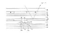
図6に従来例に係る液晶表示装置の一表示画素の回路構成図を示す。絶縁性基板(不図示)上に、ゲート信号線51、ドレイン信号線61とが交差して形成されており、その交差部近傍に両信号線51、61に接続されたTFT65が設けられている。TFT65のソース11sは液晶21の表示電極80に接続されている。
【0004】
また、表示電極80の電圧を1フィールド期間、保持するための補助容量85が設けられており、この補助容量85の一方の端子86はTFT65のソース11sに接続され、他方の電極87には各表示画素に共通の電位が印加されている。
ここで、ゲート信号線51に走査信号が印加されると、TFT65はオン状態となり、ドレイン信号線61からアナログ映像信号が表示電極80に伝達されると共に、補助容量85に保持される。表示電極80に印加された映像信号電圧が液晶21に印加され、その電圧に応じて液晶21が配向することにより液晶表示を得ることができる。
したがって、動画像、静止画像に関係なく表示を得ることができる。かかる液晶表示装置に静止画像を表示する場合、例えば携帯電話の液晶表示部の一部に携帯電話を駆動するためのバッテリの残量表示として、乾電池の画像を表示することになる。
【0005】
しかしながら、上述した構成の液晶表示装置においては、静止画像を表示する場合であっても、動画像を表示する場合と同様に、走査信号でTFT65をオン状態にして、映像信号を各表示画素に再書き込みする必要が生じていた。
そのため、走査信号及び映像信号等の駆動信号を発生するためのドライバ回路、及びドライバ回路の動作タイミングを制御するための各種信号を発生する外部LSIは常時動作するため、常に大きな電力を消費していた。このため、限られた電源しか備えていない携帯電話等では、その使用可能時間が短くなるという欠点があった。
【0006】
これに対して、各表示画素にスタティック型メモリを備えた液晶表示装置が特開平8−194205号に開示されている。同公報の一部を引用して説明すると、この液晶表示装置は、図7に示すように、2段インバータINV1,INV2を正帰還させた形のメモリ、即ちスタティック型メモリをデジタル映像信号の保持回路として用いることにより、消費電力を低減するものである。
ここで、スタティック型メモリに保持された2値デジタル映像信号に応じて、スイッチ素子24は参照線Vrefと表示電極80との間の抵抗値を制御し、液晶21のバイアス状態を調整している。一方、共通電極には交流信号Vcomを入力する。本装置は理想上、静止画像のように表示画像に変化がなければ、メモリへのリフレッシュは不要である。
【0007】
【発明が解決しようとする課題】
上述したように、従来の液晶表示装置ではアナログ映像信号に対応してフルカラーの動画像を表示するのに適している。一方、デジタル映像信号を保持するためのスタティック型メモリを備えた液晶表示装置では、低階調度の静止画像を表示すると共に、消費電力を低減するのに適している。
【0008】
しかしながら、両液晶表示装置は映像信号源を異にしているため、1つの表示装置において、フルカラーの動画像表示と、静止画像表示とを同時に実現することができなかった。また、スタティック型メモリを備えた液晶表示装置で静止画像表示を行う場合、液晶表示装置に各種の制御信号を出力する外部LSIの低消費電力化の試みはなされていなかった。
【0009】
そこで、本発明の目的とするところは、1つの表示装置(例えば、1枚の液晶表示パネル)でフルカラーの動画像表示と、低消費電力の静止画像表示という2種類の表示に対応することを可能とすることである。
【0010】
また、本発明の他の目的は、表示装置に外付けされた外部LSIを含めた表示システム全体の大幅な低消費電力を図ることである。
【0011】
【課題を解決するための手段】
本願に開示される発明のうち、主なものは以下の通りである。
【0012】
本発明の表示装置(請求項1)は、基板上の一方向に配置された複数のゲート信号線と、前記ゲート信号線に順次走査信号を供給するゲートドライバと、前記ゲート線と交差する方向に配置された複数のドレイン信号線と、前記ドレイン信号線を順次選択し、該ドレイン信号線に映像信号を供給するドレインドライバと、
前記ゲートドライバもしくは/及びドレインドライバにタイミング制御信号を供給するタイミング制御回路と、マトリックス状に配置され、前記ゲート信号線からの走査信号により選択されると共に前記ドレイン信号線から映像信号が供給される表示電極とを有する表示装置において、
前記表示電極毎に配置され、逐次入力される映像信号を前記表示電極に逐次供給する第1の表示回路と、前記表示電極に対応して配置され、映像信号を保持する保持回路を備え、該保持回路が保持した信号に応じた電圧を前記表示電極に供給する第2の表示回路と、回路選択信号に応じて、第1及び第2の表示回路を選択する回路選択回路と、を備え、前記第2の表示回路が選択された時において、動作が不要な所定回路への電源電圧の供給を停止する回路を備えることを特徴とする。
【0013】
また、如何なる回路へ電源電圧の供給を停止するかについて、好ましい実施態様は以下の通りである。
【0014】
入力デジタル映像信号をアナログ映像信号に変換するDA変換回路を更に備え、前記第2の表示回路が選択された時において、前記DA変換回路への電源電圧の供給を停止することである。DA変換回路は比較的大きな電力を消費するため、電力の削減効果は大である。
【0015】
また、アナログ映像信号を増幅する増幅回路を更に備え、前記第2の表示回路が選択されたときにおいて、前記増幅回路への電源電圧の供給を停止することである。増幅回路も比較的大きな電力を消費するため、電力の削減効果は大である。
【0016】
さらに、前記第2の表示回路が選択された時において、前記ゲートドライバもしくは/及びドレインドライバへの電源電圧の供給を停止することである。
ゲートドライバ、ドレインドライバもまた比較的大きな電力を消費するため、電力の削減効果は大である。
【0017】
また、デジタル表示モード時において前記表示パネル内のドライバへの電源電圧の供給を停止する。
【0018】
また、請求項1の表示装置に加えて、前記タイミング制御回路は前記表示パネルの液晶の対向電極に供給される第1の交流駆動信号を発振し、該第1の交流駆動信号に比較して長周期の第2の交流駆動信号を発生する発振器と、前記第2の表示回路が選択された時において、前記タイミング制御回路から前記第2の交流駆動信号に切り換える第3の切換回路と、を備えることである。
【0019】
対向電極には液晶の劣化防止のため交流駆動信号を供給する必要があるが、デジタル表示モード時においては、表示パネルのフリッカーが問題とならないため、
アナログ表示モード時に比べて長周期の交流駆動信号でも十分である。
【0020】
そこで、前記モード切換信号に応じて、前記第1及び第2の交流駆動信号とを切り換えることにより、デジタル表示モード時の消費電力を低減することができる。ここで、第2の交流駆動信号の周期は一垂直期間以上であることが低消費電力化の点で好ましい。
【0021】
また、前記第2の表示回路が選択された時において、前記タイミング制御回路への電源電圧の供給を停止する。タイミング制御回路とは別個に、第2の交流駆動信号を発生する発振器を備えているので、タイミング制御回路への電源電圧の供給を停止しても問題ない。これにより、デジタル表示モード時の消費電力を更に低減することができる。
【0022】
【発明の実施の形態】
次に、本発明の実施形態に係る表示装置について説明する。図1に本発明の表示装置を液晶表示装置に適用した場合の回路構成図を示す。
【0023】
301はフリップフロップ302,303から成るDFFである。初段のフリップフロップ302に入力されるデジタル表示モード切換信号DHが、「H(ハイ)」になると、タイミングコントローラ305からの垂直期間終了信号Vendに同期して、フリップフロップ302はモード切り換え信号MDを出力する。
【0024】
また、次の垂直期間終了信号Vendに同期して、フリップフロップ303は停止制御信号LAを出力する。モード切換信号MD、停止制御信号LAは後述する各回路の動作を制御する。
【0025】
タイミングコントローラ305はシステムクロックCLK、水平同期信号Hsync、垂直同期信号Vsyncに基づいて、パネル制御信号PC、垂直期間終了信号Vend、表示パネル100に収納された液晶の対向電極を反転駆動するための交流駆動信号FRP、DAコンバータ310の動作クロックDACCLKを出力する。ここで、上記のパネル制御信号PCにはパネル走査信号のトリガ信号となる水平スタートパルスSTH、垂直スタートパルスSTVが含まれる。
【0026】
ANDゲート306はタイミングコントローラ305の動作を停止させるための信号を出力する。このANDゲートには上記の停止制御信号LA及びデジタル表示モード切換信号DHが入力されている。したがって、タイミングコントローラ305は両信号が「H」のとき動作が停止する(デジタル表示モード時)。また、デジタル表示モード切換信号DHが「L」になると、停止状態が解除され、アナログ表示モードへ復帰可能に構成されている。
【0027】
また、タイミングコントローラ305とは独立して発振器307が設けられている。発振器307は、デジタル表示モード時の交流駆動信号の信号源となるもので、タイミングコントローラ305が出力する交流駆動信号FRPの信号周期(通常は一水平期間)に比して長周期の交流駆動信号を発生する。
【0028】
ここで、デジタル表示モード時には、後述するように、デジタル映像信号をスタティックな保持回路によって保持すると共に、その保持信号に応じて表示電極に印加する信号を選択するという構成を採用しているので、アナログ表示モード時のように補助容量のリークによる映像信号の減衰のおそれがないため、比較的低周波の交流駆動信号で足りるのである。そして、その信号周期は一垂直期間(60HZに相当する)以上であることが低消費電力化のために好ましい。
【0029】
発振器307の出力と、タイミングコントローラ305が出力する交流駆動信号FRPとはモード切換信号MDに応じて、切換回路SW3によって切り換えられ演算増幅器308によって増幅された後に対向電極端子COMに入力される。また、発振器307の出力信号はインバータ回路309によって位相が反転され、さらに演算増幅器315によって増幅された後に信号端子LSIGに入力される。これら2つの逆位相の信号ペアは後述するようにデジタル表示モードにおいて、「白」又は「黒」を表示するために利用される。
【0030】
DAコンバータ310は外部から入力されるR,G,Bのデジタル映像信号データをアナログ映像信号に変換する。ここで、R,G,Bの各デジタル映像信号データは通常8ビット構成である。その最上位ビットとDA変換され更に演算増幅器311によって増幅されたアナログ映像信号は、切換回路SW1に入力される。そして両信号は、モード切換信号MDに応じて切換回路SW1によって切り換えられ、表示パネル100のR,G,B端子へと出力される。
【0031】
なお、本実施の形態では後述する表示パネル100内のデジタル映像信号データを保持するための保持回路が1ビット構成になっているため、最上位ビットのみを出力する構成になっているが、保持回路を多ビット構成にすればそれに応じた多ビットのデジタル映像信号を出力する構成に変更することができる。
【0032】
また、切換回路SW2はモード切換信号MDに応じて、表示パネル100の端子LVDDに「H」又は「L」を出力する。これに応じて、表示パネル100は後述するように、アナログ表示モード(LVDD=「L」)、デジタル表示モード(LVDD=[H])に切り換えられる。
【0033】
また、電源回路320は電源入力に基づいて、電源電圧VDD1,VDD2(例えば5V)、VCC1,VCC2(例えば8〜10V)、VEE1,VEE2(例えば−4〜−5V)を生成する。電源回路320の各電源出力線321,322,323には切換回路SW4,SW5,SW6が設けられ、前述したANDゲート306の出力に応じて開閉し、所定回路へのVDD1、VCC1、VEE1の供給を制御可能に構成されている。
【0034】
ここで、ANDゲート306の出力が「H」になると、切換回路SW4,SW5,SW6が開き、電源電圧VDD1,VCC1,VEE1が供給された回路、即ちDAコンバータ310、演算増幅器311、タイミングコントローラ305、表示パネル100の内部ドライバへの電源供給が停止される。
【0035】
次に、上述した構成の表示装置の動作について図2のタイミング図を参照しながら説明する。デジタル表示モード切換信号DHが「H」に切り換えられると、垂直期間が終了したタイミングで発生する垂直期間信号Vendの立ち上がりに同期して、モード切換信号MDが「H」に立ち上がる。
【0036】
すると、切換回路SW3により端子LVDDが「H」に立ち上がり、表示パネル100はデジタル表示モードに切り換えられる。同時に、切換回路SW1が切り換えられ、最上位ビットのデジタル映像信号データがR,G,B端子に出力される。また、切換回路SW2により交流駆動信号(対向電極端子COMに入力される信号)が低周波に切り換えられる。こうして、一垂直期間(次のVendが立ち上がるまでの期間)をかけて、表示パネル100の1フィールドにデジタル映像信号データが書き込まれる。
【0037】
書き込みのための一垂直期間が終了し、次の信号Vendが到来すると、これに同期して停止制御信号LAが立ち上がる。すると、ANDゲート306の出力が「H」に立ち上がり、これに基づいてタイミングコントローラ305の動作が停止する。すなわち、各種パネル制御信号PC、DAコンバータ310への動作クロックDACCLK等の出力信号が固定される。これにより、DAコンバータ310の動作も停止する。
【0038】
さらに、ANDゲート306の出力が「H」に立ち上がると、切換回路SW4,SW5,SW6が開き、DAコンバータ310、演算増幅器311、タイミングコントローラ305、表示パネル100の内部ドライバへの電源供給が停止される。
【0039】
このように本発明によれば、デジタル表示モードにおいて不要な回路の動作を停止させるだけでなく、電源電圧の供給を停止しているので、回路の静消費電流も無くすことができ、大幅に消費電力を低減することができる。その効果は、動作を停止させるだけの場合の約1/5である。
【0040】
次に、アナログ表示モードに復帰させる場合には、デジタル表示モード切換信号DHが「L」に切り換えられる。すると、ANDゲート306の出力が「L」になるので、タイミングコントローラ305が再び動作を開始する。また、モード切換信号MDが「L」に立ち下がると、切換回路SW1はアナログ映像信号を出力するように切り換わる。同時に、切換回路SW2はタイミングコントローラ305からの交流駆動信号FRPを端子COMへ出力するように切り換えられる。さらに切換回路SW3はVEE側に切り換えられ、表示パネル100は通常のアナログ表示モードに設定される。
【0041】
また、ANDゲート306の出力が「L」になると、切換回路SW4,SW5,SW6が閉じ、DAコンバータ310、演算増幅器311、タイミングコントローラ305、表示パネル100の内部ドライバへの電源供給が再開される。こうして、表示パネル100は、通常のアナログ表示モードに復帰する。
【0042】
次に上述した表示パネル100本体の回路構成について図3を参照しながら詳しく説明する。絶縁基板10上に、走査信号を供給するゲートドライバ50に接続された複数のゲート信号線51が一方向に配置されており、これらのゲート信号線51と交差する方向に複数のドレイン信号線61が配置されている。
【0043】
ドレイン信号線61には、ドレインドライバ60から出力されるサンプリングパルスのタイミングに応じて、サンプリングトランジスタSP1,SP2,…,SPnがオンし、データ信号線62のデータ信号が供給される。ここで、データ信号線62のデータ信号は、前述した表示パネル100の外部の切換回路SW1の切り換えに応じて供給されるデジタル映像信号又はアナログ映像信号である(図1)。
【0044】
液晶表示パネル100は、ゲート信号線51からの走査信号により選択されると共に、ドレイン信号線61からのデータ信号が供給される複数の表示画素200がマトリックス状に配置されて構成されている。
【0045】
以下、表示画素200の詳細な構成について説明する。ゲート信号線51とドレイン信号線61の交差部近傍には、Pチャネル型TFT41及びNチャネル型42から成る回路選択回路40が設けられている。TFT41,42の両ドレインはドレイン信号線61に接続されると共に、それらの両ゲートは選択信号線88に接続されている。TFT41,42は、選択信号線88からの選択信号に応じていづれか一方がオンする。また、後述するように回路選択回路40と対を成して、回路選択回路43が設けられている。ここで、選択信号線88は、表示パネル100の端子LVDDから配線された信号線である。
【0046】
回路選択回路40,43により、後述するアナログ映像信号表示(フルカラー動画像対応)とデジタル映像表示(低消費電力、静止画像対応)とを選択して切換えることが可能となる。また、回路選択回路40に隣接して、Nチャネル型TFT71及びNチャネル型TFT72から成る画素選択回路70が配置されている。TFT71,72はそれぞれ回路選択回路40のTFT41,42と縦列に接続されると共に、それらの両ゲートにはゲート信号線51が接続されている。TFT71,72はゲート信号線51からの走査信号に応じて両方が同時にオンするように構成されている。
【0047】
また、アナログ映像信号を保持するための補助容量85が設けられている。補助容量85の一方の電極86はTFT71のソース71sに接続されている。他方の電極87は共通の補助容量線88に接続され、バイアス電圧VSCが供給されている。回路選択回路70の各TFTのゲートが開いてアナログ映像信号が液晶21に印加されると、その信号は1フィールド期間保持されなければならないが、液晶21のみではその信号の電圧は時間経過とともに次第に低下してしまう。そうすると、表示むらとして現れてしまい良好な表示が得られなくなる。そこでその電圧を1フィールド期間保持するために補助容量85を設けている。
【0048】
この補助容量85と液晶21との間には、回路選択回路43のPチャネル型TFT44が設けられ、回路選択回路43のTFT41と同時にオンオフするように構成されている。
【0049】
また、画素選択回路70のTFT72と液晶21の表示電極80との間には、保持回路110、信号選択回路120が設けられている。保持回路110は、正帰還された2つのインバータ回路から成り、デジタル2値を保持するスタティック型メモリを構成している。
【0050】
また、信号選択回路120は、保持回路110からの信号に応じて信号を選択する回路であって、2つのNチャネル型TFT121、122で構成されている。TFT121、122のゲートには保持回路110からの相補的な出力信号がそれぞれ印加されているので、TFT121、122は相補的にオンオフする。
【0051】
ここで、TFT122がオンすると交流駆動信号(信号B)が選択され、TFT121がオンすると、対向電極信号VCOM(信号A)が選択され、回路選択回路43のTFT45を介して、液晶21に電圧を印加する表示電極80に供給される。ここで、対向電極信号VCOM(信号A)は前述した発振器307からの信号に相当し、信号Bは前述した発振器307の出力が反転された信号に相当している。
【0052】
上述した構成を要約すれば、画素選択素子であるTFT71及びアナログ映像信号を保持する補助容量85から成る回路(第1の表示装置)と、画素選択素子であるTFT72、2値のデジタル映像信号を保持する保持回路110、信号選択回路12から成る回路(第2の表示装置)とが1つの表示画素200内に設けられ、更に、これら2つの回路を選択するための回路選択回路40,43が設けられている。
【0053】
次に、液晶パネル200の周辺回路について説明する。液晶パネル200の絶縁性基板10とは別基板の外付け回路基板90には、パネル駆動用LSI91が設けられている。この外付け回路基板90のパネル駆動用LSI91から垂直スタート信号STVがゲートドライバ50に入力され、水平スタート信号STHがドレインドライバ60に入力される。また映像信号がデータ線62に入力される。ここで、パネル駆動用LSI91は前述したタイミングコントローラ305に相当するものである。
【0054】
次に、図1乃至図4を参照しながら、上述した構成の表示パネルの駆動方法について説明する。図4は、液晶表示装置がデジタル表示モードに選択された場合のタイミング図である。
(1)アナログ表示モードの場合
モード切換信号MD(「L」)に応じて、アナログ表示モードが選択されると、切換回路SW1により、データ信号線62にアナログ映像信号が出力される状態に設定されると共に、回路選択信号線88の電位が「L」となり、回路選択回路40,43のTFT41,44がオンする。
【0055】
また、水平スタート信号STHに基づくサンプリング信号に応じてサンプリングトランジスタSPがオンしデータ信号線62のアナログ映像信号がドレイン信号線61に供給される。
【0056】
また、垂直スタート信号STVに基づいて、走査信号がゲート信号線51に供給される。走査信号に応じて、TFT71がオンすると、ドレイン信号線61からアナログ映像信号Sigが表示電極80に伝達されると共に、補助容量85に保持される。表示電極80に印加された映像信号電圧が液晶21に印加され、その電圧に応じて液晶21が配向することにより液晶表示を得ることができる。
【0057】
このアナログ表示モードでは、映像信号電圧を逐次入力するので、フルカラーの動画像を表示するのに好適である。ただし、外付け回路基板90のLSI91、各ドライバ50,60にはそれらを駆動するために、絶えず電力が消費されている。
(2)デジタル表示モード
モード信号切換信号MD(「H」)に応じて、デジタル表示モードが選択されると、データ信号線62にデジタル映像信号が出力される状態に設定されると共に、回路選択信号線88の電位が「H」となり、保持回路110が動作可能な状態になる。また、回路選択回路40,43のTFT41,44がオフすると共に、TFT42,45がオンする。
【0058】
また、外付け回路基板90のパネル駆動用LSI91(タイミングコントローラ305)から、ゲートドライバ50及びドレインドライバ60にスタート信号STV,STHが入力される。それに応じてサンプリング信号が順次発生し、それぞれのサンプリング信号に応じてサンプリングトランジスタSP1,SP2,…,SPnが順にオンしてデジタル映像信号Sigをサンプリングして各ドレイン信号線61に供給する。
【0059】
ここで第1行、即ち走査信号G1が印加されるゲート信号線51について説明する。まず、走査信号G1によってゲート信号線51に接続された各表示画素P11、P12、…P1nの各TFTが1水平走査期間オンする。
【0060】
第1行第1列の表示画素P11に注目すると、サンプリング信号SP1によってサンプリングしたデジタル映像信号S11がドレイン信号線61に入力される。そしてTFT72が走査信号G1によってオン状態になるとそのドレイン信号D1が保持回路110に入力される。
【0061】
この保持回路110で保持された信号は、信号選択回路120に入力されて、この信号選択回路120で信号A又は信号Bを選択して、その選択した信号が表示電極80に印加され、その電圧が液晶21に印加される。
【0062】
こうしてゲート信号線51から最終行のゲート信号線51まで走査することにより、1画面分(1フィールド期間)のスキャン、即ち全ドットスキャンによるデジタル信号の書き込みが終了し、保持回路110に書き込まれたデジタル映像信号に応じた1画面が表示される。
【0063】
ここで、1画面が表示されると、前述したように、停止制御信号LAに基づいて、ゲートドライバ50並びにドレインドライバ60、外付けのパネル駆動用LSI91(タイミングコントローラ305)等の不要な回路への電圧供給を停止しそれらの駆動を止める。
【0064】
保持回路110には常に電圧VDD,VSSを供給して駆動し、また、低周波の交流駆動信号VCOM(例えば60Hz)を液晶21の対向電極32に、各信号A及び信号Bを選択回路120に供給する。即ち、対向電極32には交流駆動信号VCOM印加し、液晶表示パネル100がノーマリーホワイト(NW)の場合には、信号Aには対向電極32と同じ交流駆動信号VCOMを印加し、信号Bには信号Aと逆位相の交流駆動信号が印加される。
【0065】
このとき、ドレイン信号線61にデジタル映像信号で「H(ハイ)」が保持回路110に入力された場合には、信号選択回路120において第1のTFT121には「L」が入力されることになるので第1のTFT121はオフとなり、他方の第2のTFT122には「H」が入力されることになるので第2のTFT122はオンとなる。
【0066】
そうすると、信号Bが選択されて液晶の表示電極80には、対向電極32と逆位相の信号Bの電圧が印加され、液晶が電界によって立ち上がるため、ノーマリーホワイトの表示パネルでは表示としては黒表示として観察できる。
【0067】
ドレイン信号線61にデジタル映像信号で「L」が保持回路110に入力された場合には、信号選択回路120において第1のTFT121には「H」が入力されることになるので第1のTFT121はオンとなり、他方の第2のTFT122には「L」が入力されることになるので第2のTFT122はオフとなる。そうすると、信号Aが選択されて液晶には信号Aが印加される。即ち、対向電極32と同じ位相の信号が印加されるため、電界が発生せず液晶は立ち上がらないため、ノーマリーホワイトの表示パネルでは表示としては白表示として観察できる。
【0068】
このデジタル表示モードにおいては、1画面分を書き込みそれを保持することにより静止画像として表示でき、各ドライバ50,60及びLSI91等の駆動、及び電源の供給を停止するので、大幅に低消費電力化することができる。
【0069】
本発明の表示装置は、液晶表示装置の中でも特に、反射型液晶表示装置に適用することが好ましい。そこで、この反射型液晶表示装置のデバイス構造について図5を参照しながら説明する。
【0070】
図5に示すように、一方の絶縁性基板10上に、多結晶シリコンから成り島化された半導体層11上にゲート絶縁膜12を形成し、半導体層11の上方であってゲート絶縁膜12上にゲート電極13を形成する。
【0071】
ゲート電極13の両側に位置する下層の半導体層11には、ソース11s及びドレイン11dが形成されている。ゲート電極13及びゲート絶縁膜12上には層間絶縁膜14を堆積し、そのドレイン11dに対応した位置及びソース11sに対応した位置にコンタクトホール15が形成されており、そのコンタクトホール15を介してドレイン11dはドレイン電極16に接続されており、ソース11sは層間絶縁膜14上に設けた平坦化絶縁膜17に設けたコンタクトホール18も介して表示電極19に接続されている。
【0072】
平坦化絶縁膜17上に形成された各表示電極19はアルミニウム(Al)等の反射材料から成っている。各表示電極19及び平坦化絶縁膜17上には液晶21を配向するポリイミド等から成る配向膜20が形成されている。
【0073】
他方の絶縁性基板30上には、赤(R)、緑(G)、青(B)の各色を呈するカラーフィルタ31、ITO(Indium Tin Oxide)等の透明導電性膜から成る対向電極32、及び液晶21を配向する配向膜33が順に形成されている。カラー表示としない場合にはカラーフィルタ31は不要である。
【0074】
こうして形成された一対の絶縁性基板10,30の周辺を接着性シール材によって接着し、それによって形成された空隙に液晶21を充填して、反射型液晶表示装置が完成する。
【0075】
図中点線矢印で示すように、観察者1側から入射した外光は、対向電極基板30から順に入射し、表示電極19によって反射されて、観察者1側に出射し、表示を観察者1が観察することができる。
【0076】
このように、反射型液晶表示装置は外光を反射させて表示を観察する方式であり、透過型の液晶表示装置のように、観察者側と反対側にいわゆるバックライトを用いる必要が無いため、そのバックライトを点灯させるための電力を必要としない。従って、本発明の表示装置として、バックライト不要で低消費電力化に適した反射型液晶表示装置であることが好ましい。
【0077】
上述の実施の形態においては、1画面の全ドットスキャン期間には、対向電極電圧及び信号A及びBの電圧は印加している場合について示したが、本発明はそれに限定されるものではなく、この期間においてもこれらの各電圧を印加しなくても良い。しかしながら消費電力を低減させるためには、好ましくは印加しない方が良い。
【0078】
また、上述の実施の形態においては、デジタル表示モードにおいて、1ビットのデジタルデータ信号を入力した場合について説明したが、本発明はそれに限定されるものではなく、複数ビットのデジタルデータ信号の場合でも適用することが可能である。そうすることにより、多階調の表示を行うことができる。その際、入力するビット数に応じた保持回路及び信号選択回路の数にする必要がある。
【0079】
また、上述の実施の形態においては、静止画像を液晶表示パネルの一部に表示する場合を説明したが、本願はそれに限定されるものではなく、全表示画素に静止画を表示することも可能であり、本願発明の特有の効果を奏するものである。
【0080】
上述の実施の形態においては、反射型液晶表示装置の場合について説明したが、1画素内でTFT、保持回路、信号選択回路及び信号配線を除く領域に透明電極を配置することにより、透過型液晶表示装置にも用いることができる。
【0081】
【発明の効果】
本発明の表示装置によれば、1つの表示パネルで、アナログ表示モードによるフルカラーの動画像表示と、デジタル表示モードによる低消費電力対応の階調数の少ない静止画像表示という2種類の表示を選択することが可能なる。
【0082】
特に、デジタル表示モードが選択された場合には、不要な回路への動作を停止するだけでなく、電源供給を停止しているので、表示装置全体としての消費電力を大幅に低減することができる。
【0083】
これにより、バッテリ等の限られた電源を用いた携帯用テレビ、携帯電話に本発明の表示装置を用いた場合にも消費電力が少ないので長時間の表示を可能とすることができる。
【図面の簡単な説明】
【図1】本発明の実施形態に係る液晶表示装置の回路構成図である。
【図2】本発明の実施形態に係る映像信号の切換回路の回路構成図である。
【図3】本発明の実施形態に係る液晶表示装置の他の回路構成図である。
【図4】本発明の実施形態に係る液晶表示装置のタイミング図である。
【図5】反射型液晶表示装置の断面図である。
【図6】従来例に係る液晶表示装置の回路構成図である。
【図7】従来例に係る液晶表示装置の他の回路構成図である。
【符号の説明】
301 DFF
305 タイミングコントローラ
306 ANDゲート
310 DAコンバータ
320 電源回路
10 絶縁性基板
13 ゲート
21 液晶
40 回路選択回路
43 回路選択回路
50 ゲートドライバ
51 ゲート信号線
60 ドレインドライバ
61 ドレイン信号線
70 画素選択回路
85 補助容量
110 保持回路
120 信号選択回路[0001]
BACKGROUND OF THE INVENTION
The present invention relates to a display device, and more particularly to a display device suitable for use in a portable display device.
[0002]
[Prior art]
In recent years, portable display devices such as mobile TVs and mobile phones have been required as market needs. In response to such demands, research and development has been actively conducted to cope with the reduction in size, weight, and power consumption of display devices.
[0003]
FIG. 6 shows a circuit configuration diagram of one display pixel of a liquid crystal display device according to a conventional example. A
[0004]
Further, an
Here, when a scanning signal is applied to the
Therefore, a display can be obtained regardless of a moving image or a still image. When a still image is displayed on such a liquid crystal display device, for example, an image of a dry cell is displayed as a battery remaining amount display for driving the mobile phone on a part of the liquid crystal display unit of the mobile phone.
[0005]
However, in the liquid crystal display device having the above-described configuration, even when a still image is displayed, the TFT 65 is turned on by a scanning signal and a video signal is sent to each display pixel as in the case of displaying a moving image. There was a need to rewrite.
For this reason, driver circuits for generating drive signals such as scanning signals and video signals, and external LSIs for generating various signals for controlling the operation timing of the driver circuits always operate, and thus always consume large power. It was. For this reason, a mobile phone or the like having only a limited power source has a drawback that the usable time is shortened.
[0006]
On the other hand, a liquid crystal display device having a static memory in each display pixel is disclosed in Japanese Patent Laid-Open No. 8-194205. Describing a part of the publication, this liquid crystal display device, as shown in FIG. 7, retains a digital video signal in a memory in which two-stage inverters INV1 and INV2 are positively fed back, that is, a static memory. By using it as a circuit, power consumption is reduced.
Here, according to the binary digital video signal held in the static memory, the
[0007]
[Problems to be solved by the invention]
As described above, the conventional liquid crystal display device is suitable for displaying a full-color moving image corresponding to an analog video signal. On the other hand, a liquid crystal display device having a static memory for holding a digital video signal is suitable for displaying a still image with a low gradation and reducing power consumption.
[0008]
However, since both liquid crystal display devices have different video signal sources, full color moving image display and still image display cannot be realized simultaneously in one display device. In addition, when a still image is displayed on a liquid crystal display device having a static memory, no attempt has been made to reduce the power consumption of an external LSI that outputs various control signals to the liquid crystal display device.
[0009]
Therefore, an object of the present invention is to support two types of display, that is, full-color moving image display and low power consumption still image display with one display device (for example, one liquid crystal display panel). It is possible.
[0010]
Another object of the present invention is to significantly reduce power consumption of the entire display system including an external LSI externally attached to the display device.
[0011]
[Means for Solving the Problems]
Among the inventions disclosed in the present application, main ones are as follows.
[0012]
A display device according to the present invention (Claim 1) includes a plurality of gate signal lines arranged in one direction on a substrate, a gate driver for sequentially supplying a scanning signal to the gate signal lines, and a direction intersecting the gate lines. A plurality of drain signal lines disposed on the drain signal line; and a drain driver that sequentially selects the drain signal lines and supplies a video signal to the drain signal lines;
A timing control circuit for supplying a timing control signal to the gate driver or / and the drain driver, and a matrix, which are selected by a scanning signal from the gate signal line and are supplied with a video signal from the drain signal line In a display device having a display electrode,
A first display circuit that is arranged for each display electrode and sequentially supplies video signals that are sequentially input to the display electrode; and a holding circuit that is arranged corresponding to the display electrodes and holds the video signal, A second display circuit for supplying a voltage corresponding to the signal held by the holding circuit to the display electrode, and a circuit selection circuit for selecting the first and second display circuits according to the circuit selection signal, When the second display circuit is selected, a circuit for stopping supply of power supply voltage to a predetermined circuit that does not require operation is provided.
[0013]
A preferred embodiment of the circuit to which the supply of the power supply voltage is stopped is as follows.
[0014]
A DA conversion circuit for converting an input digital video signal into an analog video signal is further provided, and supply of power supply voltage to the DA conversion circuit is stopped when the second display circuit is selected. Since the DA converter circuit consumes relatively large power, the power reduction effect is great.
[0015]
Further, an amplifier circuit for amplifying the analog video signal is further provided, and supply of the power supply voltage to the amplifier circuit is stopped when the second display circuit is selected. Since the amplifier circuit also consumes a relatively large amount of power, the power reduction effect is significant.
[0016]
Further, when the second display circuit is selected, the supply of the power supply voltage to the gate driver or / and the drain driver is stopped.
Since the gate driver and the drain driver also consume relatively large power, the power reduction effect is great.
[0017]
In the digital display mode, the supply of power supply voltage to the driver in the display panel is stopped.
[0018]
In addition to the display device according to claim 1, the timing control circuit oscillates a first AC drive signal supplied to the counter electrode of the liquid crystal of the display panel and compares it with the first AC drive signal. An oscillator that generates a long-cycle second AC drive signal; and a third switching circuit that switches from the timing control circuit to the second AC drive signal when the second display circuit is selected. It is to prepare.
[0019]
Although it is necessary to supply an AC drive signal to the counter electrode to prevent liquid crystal deterioration, flickering of the display panel is not a problem in the digital display mode.
A long-period AC drive signal is sufficient as compared with the analog display mode.
[0020]
Therefore, the power consumption in the digital display mode can be reduced by switching between the first and second AC drive signals in accordance with the mode switching signal. Here, the period of the second AC drive signal is preferably one vertical period or more in terms of low power consumption.
[0021]
Further, when the second display circuit is selected, the supply of the power supply voltage to the timing control circuit is stopped. Since the oscillator for generating the second AC drive signal is provided separately from the timing control circuit, there is no problem even if the supply of the power supply voltage to the timing control circuit is stopped. Thereby, the power consumption in the digital display mode can be further reduced.
[0022]
DETAILED DESCRIPTION OF THE INVENTION
Next, a display device according to an embodiment of the present invention will be described. FIG. 1 shows a circuit configuration diagram when the display device of the present invention is applied to a liquid crystal display device.
[0023]
A
[0024]
Further, the flip-
[0025]
The
[0026]
The AND
[0027]
In addition, an
[0028]
Here, in the digital display mode, as will be described later, the digital video signal is held by a static holding circuit, and a configuration is adopted in which a signal applied to the display electrode is selected according to the holding signal. Since there is no risk of attenuation of the video signal due to leakage of the auxiliary capacitor as in the analog display mode, a relatively low frequency AC drive signal is sufficient. The signal period is preferably one vertical period (corresponding to 60 Hz) or more in order to reduce power consumption.
[0029]
The output of the
[0030]
The
[0031]
In this embodiment, since a holding circuit for holding digital video signal data in the
[0032]
Further, the switching circuit SW2 outputs “H” or “L” to the terminal LVDD of the
[0033]
The
[0034]
Here, when the output of the AND
[0035]
Next, the operation of the display device having the above-described configuration will be described with reference to the timing chart of FIG. When the digital display mode switching signal DH is switched to “H”, the mode switching signal MD rises to “H” in synchronization with the rising of the vertical period signal Vend generated at the timing when the vertical period ends.
[0036]
Then, the terminal LVDD rises to “H” by the switching circuit SW3, and the
[0037]
When one vertical period for writing ends and the next signal Vend arrives, the stop control signal LA rises in synchronization therewith. Then, the output of the AND
[0038]
Further, when the output of the AND
[0039]
As described above, according to the present invention, not only the operation of unnecessary circuits in the digital display mode is stopped, but also the supply of the power supply voltage is stopped. Electric power can be reduced. The effect is about 1/5 of the case where the operation is merely stopped.
[0040]
Next, when returning to the analog display mode, the digital display mode switching signal DH is switched to “L”. Then, since the output of the AND
[0041]
Further, when the output of the AND
[0042]
Next, the circuit configuration of the
[0043]
Sampling transistors SP1, SP2,..., SPn are turned on according to the timing of the sampling pulse output from the
[0044]
The liquid
[0045]
Hereinafter, a detailed configuration of the
[0046]
The
[0047]
In addition, an
[0048]
A P-
[0049]
A holding
[0050]
The
[0051]
Here, when the
[0052]
To summarize the above-described configuration, a circuit (first display device) including a
[0053]
Next, peripheral circuits of the
[0054]
Next, a method for driving the display panel having the above-described configuration will be described with reference to FIGS. FIG. 4 is a timing chart when the liquid crystal display device is selected in the digital display mode.
(1) In the case of the analog display mode When the analog display mode is selected according to the mode switching signal MD (“L”), the switching circuit SW1 sets the state in which the analog video signal is output to the data signal
[0055]
Further, the sampling transistor SP is turned on according to the sampling signal based on the horizontal start signal STH, and the analog video signal of the data signal
[0056]
A scanning signal is supplied to the
[0057]
In this analog display mode, the video signal voltage is sequentially input, which is suitable for displaying a full-color moving image. However, the
(2) When the digital display mode is selected according to the digital display mode mode signal switching signal MD (“H”), the digital video signal is set to be output to the data signal
[0058]
Further, start signals STV and STH are input to the
[0059]
Here, the first row, that is, the
[0060]
When attention is paid to the display pixel P11 in the first row and first column, the digital video signal S11 sampled by the sampling signal SP1 is inputted to the
[0061]
The signal held by the holding
[0062]
By scanning from the
[0063]
Here, when one screen is displayed, as described above, based on the stop control signal LA, to unnecessary circuits such as the
[0064]
The holding
[0065]
At this time, when “H (high)” is input to the
[0066]
Then, the signal B is selected, and the voltage of the signal B having the opposite phase to the
[0067]
When “L” is input to the
[0068]
In this digital display mode, it can be displayed as a still image by writing and holding one screen, and driving of each
[0069]
The display device of the present invention is preferably applied to a reflective liquid crystal display device among liquid crystal display devices. The device structure of this reflective liquid crystal display device will be described with reference to FIG.
[0070]
As shown in FIG. 5, on one insulating
[0071]
A
[0072]
Each
[0073]
On the other insulating
[0074]
The periphery of the pair of insulating
[0075]
As indicated by the dotted arrows in the figure, the external light incident from the viewer 1 side enters from the
[0076]
Thus, the reflective liquid crystal display device is a method of observing the display by reflecting external light, and unlike the transmissive liquid crystal display device, it is not necessary to use a so-called backlight on the side opposite to the viewer side. Does not require power to turn on its backlight. Therefore, the display device of the present invention is preferably a reflective liquid crystal display device that does not require a backlight and is suitable for low power consumption.
[0077]
In the above-described embodiment, the case where the counter electrode voltage and the voltages of the signals A and B are applied during the entire dot scan period of one screen has been described, but the present invention is not limited thereto. It is not necessary to apply these voltages during this period. However, in order to reduce power consumption, it is preferable not to apply.
[0078]
In the above-described embodiment, the case where a 1-bit digital data signal is input in the digital display mode has been described. However, the present invention is not limited thereto, and even in the case of a multi-bit digital data signal. It is possible to apply. By doing so, multi-gradation display can be performed. At that time, it is necessary to set the number of holding circuits and signal selection circuits according to the number of input bits.
[0079]
In the above-described embodiment, the case where a still image is displayed on a part of a liquid crystal display panel has been described. However, the present application is not limited thereto, and a still image can be displayed on all display pixels. Thus, the present invention has a characteristic effect of the present invention.
[0080]
In the above-described embodiment, the case of the reflective liquid crystal display device has been described. However, by disposing a transparent electrode in a region excluding the TFT, the holding circuit, the signal selection circuit, and the signal wiring in one pixel, the transmissive liquid crystal It can also be used for a display device.
[0081]
【Effect of the invention】
According to the display device of the present invention, one display panel selects two types of display: full-color moving image display in the analog display mode and still image display with a low number of gradations corresponding to low power consumption in the digital display mode. It becomes possible to do.
[0082]
In particular, when the digital display mode is selected, not only the operation to unnecessary circuits is stopped, but also the power supply is stopped, so that the power consumption of the entire display device can be greatly reduced. .
[0083]
Accordingly, even when the display device of the present invention is used for a portable television or a mobile phone using a limited power source such as a battery, the display can be performed for a long time because of low power consumption.
[Brief description of the drawings]
FIG. 1 is a circuit configuration diagram of a liquid crystal display device according to an embodiment of the present invention.
FIG. 2 is a circuit configuration diagram of a video signal switching circuit according to an embodiment of the present invention.
FIG. 3 is another circuit configuration diagram of the liquid crystal display device according to the embodiment of the present invention.
FIG. 4 is a timing chart of the liquid crystal display device according to the embodiment of the invention.
FIG. 5 is a cross-sectional view of a reflective liquid crystal display device.
FIG. 6 is a circuit configuration diagram of a liquid crystal display device according to a conventional example.
FIG. 7 is another circuit configuration diagram of a liquid crystal display device according to a conventional example.
[Explanation of symbols]
301 DFF
305
Claims (6)
Translated fromJapanese前記ゲート信号線に順次走査信号を供給するゲートドライバと、
前記ゲート線と交差する方向に配置された複数のドレイン信号線と、
前記ドレイン信号線を順次選択し、該ドレイン信号線に映像信号を供給するドレインドライバと、前記ゲートドライバもしくは/及びドレインドライバにタイミング制御信号を供給するタイミング制御回路と、
マトリックス状に配置され、前記ゲート信号線からの走査信号により選択されると共に前記ドレイン信号線から映像信号が供給される表示電極とを有する表示装置において、
入力デジタル映像信号をアナログ映像信号に変換するDA変換回路と、
前記表示電極毎に配置され、逐次入力される前記アナログ映像信号を前記表示電極に逐次供給し、アナログ表示を行う第1の表示回路と、
前記表示電極に対応して配置され、前記入力デジタル映像信号を保持する保持回路を備え、該保持回路が保持した信号に応じた電圧を前記表示電極に供給し、デジタル表示を行う第2の表示回路と、
選択信号に応じて前記第1及び第2の表示回路を選択する回路選択回路と、
外部から入力されるモード設定信号に基づき、前記回路選択回路に前記選択信号を入力する制御回路を備え、
前記制御回路は、前記第2の表示回路への切換を指示する前記モード設定信号を垂直期間終了信号に応じて遅延し、停止信号を生成する遅延回路と、前記モード設定信号および前記停止信号が入力されるANDゲート回路から成り、
前記ANDゲート回路からの出力信号によって、前記第2の表示回路が選択された後に、前記DA変換回路への電源電圧の供給を停止する
ことを特徴とする表示装置。A plurality of gate signal lines arranged in one direction on the substrate;
A gate driver for sequentially supplying scanning signals to the gate signal lines;
A plurality of drain signal lines arranged in a direction crossing the gate line;
A drain driver that sequentially selects the drain signal line and supplies a video signal to the drain signal line; a timing control circuit that supplies a timing control signal to the gate driver or / and the drain driver;
In a display device having a display electrode arranged in a matrix and selected by a scanning signal from the gate signal line and supplied with a video signal from the drain signal line,
A DA conversion circuit for converting an input digital video signal into an analog video signal;
A first display circuit that is arranged for each display electrode and sequentially supplies theanalog video signals that are sequentially input to the display electrodesto perform analog display ;
A second display which is arranged corresponding to the display electrode and includes a holding circuit for holding theinput digital video signal , and supplies a voltage corresponding to the signal held by the holding circuit to the display electrodeto perform digital display Circuit,
A circuit selection circuit for selecting the first and second display circuitsin response to a selection signal ;
Based on a mode setting signal input from the outside, comprising a control circuit forinputting the selection signal to the circuit selection circuit ,
The control circuit delays themode setting signal instructing switching to the second display circuitin accordance with avertical period end signal, generates a stop signal, and themode setting signal and the stop signal are It consists of aninput AND gate circuit ,
A display device,wherein after the second display circuit is selected by an output signal from theAND gate circuit, supply of a power supply voltage to theDA converter circuit is stopped.
該第1の交流駆動信号に比較して長周期の第2の交流駆動信号を発生する発振器と、
前記第2の表示回路が選択された後において、前記タイミング制御回路から前記第2の交流駆動信号に切り換える第3の切換回路と、を備えることを特徴とする請求項1に記載の表示装置。The timing control circuit oscillates a first AC driving signal supplied to the counter electrode of the liquid crystal of the display panel,
An oscillator for generating a second AC drive signal having a long period compared to the first AC drive signal;
The display device according to claim 1, further comprising: a third switching circuit that switches from the timing control circuit to the second AC drive signal after the second display circuit is selected.
Priority Applications (7)
| Application Number | Priority Date | Filing Date | Title |
|---|---|---|---|
| JP2000282175AJP5019668B2 (en) | 2000-09-18 | 2000-09-18 | Display device and control method thereof |
| TW090119450ATW588313B (en) | 2000-09-18 | 2001-08-09 | Display apparatus and method for controlling same |
| US09/953,233US7019738B2 (en) | 2000-09-18 | 2001-09-17 | Display device and its control method |
| KR10-2001-0057105AKR100469877B1 (en) | 2000-09-18 | 2001-09-17 | Display device and method of controlling the same |
| EP01122308AEP1189192A3 (en) | 2000-09-18 | 2001-09-18 | Display device and its control method |
| CNB011331755ACN1299150C (en) | 2000-09-18 | 2001-09-18 | Display and control method thereof |
| US11/338,821US7808495B2 (en) | 2000-09-18 | 2006-01-25 | Display device and its control method |
Applications Claiming Priority (1)
| Application Number | Priority Date | Filing Date | Title |
|---|---|---|---|
| JP2000282175AJP5019668B2 (en) | 2000-09-18 | 2000-09-18 | Display device and control method thereof |
Related Child Applications (1)
| Application Number | Title | Priority Date | Filing Date |
|---|---|---|---|
| JP2011273250ADivisionJP2012063790A (en) | 2011-12-14 | 2011-12-14 | Display device |
Publications (2)
| Publication Number | Publication Date |
|---|---|
| JP2002091396A JP2002091396A (en) | 2002-03-27 |
| JP5019668B2true JP5019668B2 (en) | 2012-09-05 |
Family
ID=18766728
Family Applications (1)
| Application Number | Title | Priority Date | Filing Date |
|---|---|---|---|
| JP2000282175AExpired - LifetimeJP5019668B2 (en) | 2000-09-18 | 2000-09-18 | Display device and control method thereof |
Country Status (6)
| Country | Link |
|---|---|
| US (2) | US7019738B2 (en) |
| EP (1) | EP1189192A3 (en) |
| JP (1) | JP5019668B2 (en) |
| KR (1) | KR100469877B1 (en) |
| CN (1) | CN1299150C (en) |
| TW (1) | TW588313B (en) |
Families Citing this family (48)
| Publication number | Priority date | Publication date | Assignee | Title |
|---|---|---|---|---|
| JP4868652B2 (en)* | 2001-04-11 | 2012-02-01 | 三洋電機株式会社 | Display device |
| JP4638117B2 (en)* | 2002-08-22 | 2011-02-23 | シャープ株式会社 | Display device and driving method thereof |
| JP3873149B2 (en)* | 2002-12-11 | 2007-01-24 | 株式会社日立製作所 | Display device |
| KR100945577B1 (en) | 2003-03-11 | 2010-03-08 | 삼성전자주식회사 | Driving device of liquid crystal display and method thereof |
| US7388579B2 (en) | 2003-05-01 | 2008-06-17 | Motorola, Inc. | Reduced power consumption for a graphics accelerator and display |
| KR100737887B1 (en)* | 2003-05-20 | 2007-07-10 | 삼성전자주식회사 | Driving circuit, flat panel display having same and driving method thereof |
| JP4779288B2 (en)* | 2003-05-28 | 2011-09-28 | 富士ゼロックス株式会社 | Image display device |
| JP2005043865A (en)* | 2003-07-08 | 2005-02-17 | Seiko Epson Corp | Display device driving method and driving device |
| KR100430102B1 (en)* | 2003-10-09 | 2004-05-04 | 주식회사 케이이씨 | Gate operation circuit for liquid crystal display device |
| KR100606715B1 (en)* | 2004-04-20 | 2006-08-01 | 엘지전자 주식회사 | Liquid crystal display interface device and interfacing method of mobile communication terminal |
| KR101103889B1 (en)* | 2004-12-29 | 2012-01-12 | 엘지디스플레이 주식회사 | Liquid crystal display device and driving method thereof |
| JP2006203333A (en)* | 2005-01-18 | 2006-08-03 | Canon Inc | Bidirectional remote control unit |
| JP2006285118A (en)* | 2005-04-05 | 2006-10-19 | Hitachi Displays Ltd | Display device |
| KR101214520B1 (en) | 2005-04-26 | 2012-12-24 | 가부시키가이샤 한도오따이 에네루기 켄큐쇼 | Light emitting device and method for driving thereof |
| JP5291865B2 (en)* | 2005-05-02 | 2013-09-18 | 株式会社半導体エネルギー研究所 | Display device, display module, and electronic device |
| CN102394049B (en) | 2005-05-02 | 2015-04-15 | 株式会社半导体能源研究所 | Driving method of display device |
| JP5057694B2 (en)* | 2005-05-02 | 2012-10-24 | 株式会社半導体エネルギー研究所 | Display device, display module, and electronic device |
| US7636078B2 (en) | 2005-05-20 | 2009-12-22 | Semiconductor Energy Laboratory Co., Ltd. | Display device and electronic device |
| US8847861B2 (en) | 2005-05-20 | 2014-09-30 | Semiconductor Energy Laboratory Co., Ltd. | Active matrix display device, method for driving the same, and electronic device |
| JP5386060B2 (en)* | 2005-05-20 | 2014-01-15 | 株式会社半導体エネルギー研究所 | Display device |
| JP5386059B2 (en)* | 2005-05-20 | 2014-01-15 | 株式会社半導体エネルギー研究所 | Display device |
| US20070040789A1 (en)* | 2005-08-17 | 2007-02-22 | Samsung Electronics Co., Ltd. | Protection device for gate integrated circuit, gate driver, liquid crystal display including the same and method of protecting a gate IC in a display |
| CN101174064B (en)* | 2006-06-08 | 2010-06-02 | 友达光电股份有限公司 | Driving circuit, time sequence controller and driving method of liquid crystal display |
| KR20080036844A (en)* | 2006-10-24 | 2008-04-29 | 삼성전자주식회사 | Timing controller and liquid crystal display including the same |
| TW200822700A (en)* | 2006-11-03 | 2008-05-16 | Innolux Display Corp | Display system and display method thereof |
| US9866785B2 (en)* | 2007-08-15 | 2018-01-09 | Advanced Micro Devices, Inc. | Automatic reduction of video display device power consumption |
| JP5298284B2 (en)* | 2007-11-30 | 2013-09-25 | 株式会社ジャパンディスプレイ | Image display device and driving method thereof |
| JP5066432B2 (en)* | 2007-11-30 | 2012-11-07 | 株式会社ジャパンディスプレイイースト | Image display device |
| GB2460409B (en)* | 2008-05-27 | 2012-04-04 | Sony Corp | Driving circuit for a liquid crystal display |
| KR101717460B1 (en)* | 2009-10-16 | 2017-03-17 | 가부시키가이샤 한도오따이 에네루기 켄큐쇼 | Liquid crystal display device and electronic device including the liquid crystal display device |
| KR102143040B1 (en)* | 2009-10-16 | 2020-08-11 | 가부시키가이샤 한도오따이 에네루기 켄큐쇼 | Liquid crystal display device and electronic apparatus having the same |
| KR102257564B1 (en) | 2009-12-18 | 2021-05-31 | 가부시키가이샤 한도오따이 에네루기 켄큐쇼 | Driving method of display device and display device |
| KR102135326B1 (en)* | 2010-01-24 | 2020-07-20 | 가부시키가이샤 한도오따이 에네루기 켄큐쇼 | Display device |
| DE102010011029A1 (en)* | 2010-03-11 | 2011-09-15 | Osram Opto Semiconductors Gmbh | Portable electronic device |
| US9697788B2 (en)* | 2010-04-28 | 2017-07-04 | Semiconductor Energy Laboratory Co., Ltd. | Liquid crystal display device |
| JP2015102596A (en)* | 2013-11-21 | 2015-06-04 | ラピスセミコンダクタ株式会社 | Drive device of display device |
| CN106471566B (en)* | 2014-06-25 | 2019-01-25 | 夏普株式会社 | Display device and driving method thereof |
| US20160203798A1 (en)* | 2015-01-13 | 2016-07-14 | Vastview Technology Inc. | Liquid crystal display device having at least three electrodes in each pixel area |
| CN105068108B (en)* | 2015-07-22 | 2018-04-03 | 成都理工大学 | It is a kind of based on the multi-functional neutron and gamma detector singly popped one's head in |
| CN105407298B (en)* | 2015-10-10 | 2019-02-12 | 浙江大华技术股份有限公司 | A kind of VGA Inverse problem circuit and method |
| KR102577409B1 (en)* | 2016-08-22 | 2023-09-14 | 엘지디스플레이 주식회사 | Controller, display device, and the method for driving the display device |
| CN106935202B (en)* | 2017-05-19 | 2019-01-18 | 京东方科技集团股份有限公司 | Pixel circuit and its driving method, display device |
| CN106971686A (en)* | 2017-05-25 | 2017-07-21 | 上海中航光电子有限公司 | Display device and its driving method |
| CN107833559B (en)* | 2017-12-08 | 2023-11-28 | 合肥京东方光电科技有限公司 | Pixel driving circuit, organic light emitting display panel and pixel driving method |
| CN108877731B (en)* | 2018-09-20 | 2021-08-24 | 京东方科技集团股份有限公司 | Display panel driving method, display panel |
| CN112863415A (en)* | 2019-11-28 | 2021-05-28 | 京东方科技集团股份有限公司 | Pixel driving circuit and display device |
| KR102756227B1 (en)* | 2019-12-27 | 2025-01-17 | 엘지디스플레이 주식회사 | OLED display device and driving method therefor |
| CN111667797A (en)* | 2020-06-30 | 2020-09-15 | 联想(北京)有限公司 | Electronic equipment and control method thereof |
Family Cites Families (39)
| Publication number | Priority date | Publication date | Assignee | Title |
|---|---|---|---|---|
| JPS5823091A (en) | 1981-08-04 | 1983-02-10 | セイコーインスツルメンツ株式会社 | Picture display unit |
| JPH04107623A (en)* | 1990-08-28 | 1992-04-09 | Seiko Epson Corp | display device |
| KR950005225B1 (en)* | 1991-03-26 | 1995-05-22 | 가부시끼가이샤 히다찌세이사꾸쇼 | Data processor |
| JP2784615B2 (en)* | 1991-10-16 | 1998-08-06 | 株式会社半導体エネルギー研究所 | Electro-optical display device and driving method thereof |
| JP2557606B2 (en)* | 1992-06-04 | 1996-11-27 | 株式会社東芝 | Display control device and power down control method for the display control device |
| JP3240218B2 (en)* | 1992-08-19 | 2001-12-17 | 株式会社日立製作所 | Information processing device capable of multi-color display |
| US5537650A (en)* | 1992-12-14 | 1996-07-16 | International Business Machines Corporation | Method and apparatus for power management in video subsystems |
| JP3298301B2 (en)* | 1994-04-18 | 2002-07-02 | カシオ計算機株式会社 | Liquid crystal drive |
| CN1046164C (en)* | 1994-10-13 | 1999-11-03 | 凌阳科技股份有限公司 | Divisible LCD panel driver |
| JPH08194205A (en) | 1995-01-18 | 1996-07-30 | Toshiba Corp | Active matrix display |
| JP3630489B2 (en)* | 1995-02-16 | 2005-03-16 | 株式会社東芝 | Liquid crystal display |
| JPH08263016A (en)* | 1995-03-17 | 1996-10-11 | Semiconductor Energy Lab Co Ltd | Active matrix liquid crystal display device |
| JPH08336162A (en)* | 1995-06-08 | 1996-12-17 | Rohm Co Ltd | Rgb encoder and electronic equipment incorporated with the same |
| JP3318666B2 (en)* | 1995-09-22 | 2002-08-26 | シャープ株式会社 | Liquid crystal display |
| US5945972A (en)* | 1995-11-30 | 1999-08-31 | Kabushiki Kaisha Toshiba | Display device |
| KR100474786B1 (en)* | 1995-12-14 | 2005-07-07 | 세이코 엡슨 가부시키가이샤 | Display method of operation, display device and electronic device |
| JP3245733B2 (en)* | 1995-12-28 | 2002-01-15 | 株式会社アドバンスト・ディスプレイ | Liquid crystal display device and driving method thereof |
| JP3319561B2 (en) | 1996-03-01 | 2002-09-03 | 株式会社東芝 | Liquid crystal display |
| KR100270147B1 (en)* | 1996-03-01 | 2000-10-16 | 니시무로 타이죠 | Lcd apparatus |
| JP3305946B2 (en) | 1996-03-07 | 2002-07-24 | 株式会社東芝 | Liquid crystal display |
| EP0797182A1 (en) | 1996-03-19 | 1997-09-24 | Hitachi, Ltd. | Active matrix LCD with data holding circuit in each pixel |
| JP3261519B2 (en)* | 1996-06-11 | 2002-03-04 | 株式会社日立製作所 | Liquid crystal display |
| KR100236570B1 (en)* | 1996-05-15 | 2000-01-15 | 비센트 비.인그라시아 | Operation system and its method of liquid crystal display |
| JPH09329806A (en)* | 1996-06-11 | 1997-12-22 | Toshiba Corp | Liquid crystal display |
| JP3488577B2 (en)* | 1996-08-30 | 2004-01-19 | 株式会社東芝 | Matrix type display device |
| JPH10105132A (en)* | 1996-10-03 | 1998-04-24 | Nec Gumma Ltd | Lcd control circuits for reducing power consumption |
| US5790090A (en)* | 1996-10-16 | 1998-08-04 | International Business Machines Corporation | Active matrix liquid crystal display with reduced drive pulse amplitudes |
| US5952991A (en)* | 1996-11-14 | 1999-09-14 | Kabushiki Kaisha Toshiba | Liquid crystal display |
| GB2320345B (en)* | 1996-12-12 | 1998-11-18 | John Quentin Phillipps | Portable computer apparatus |
| KR19980060007A (en)* | 1996-12-31 | 1998-10-07 | 김광호 | Power consumption reduction circuit of liquid crystal display |
| JP3156045B2 (en)* | 1997-02-07 | 2001-04-16 | 株式会社日立製作所 | Liquid crystal display |
| JP3231696B2 (en)* | 1998-03-04 | 2001-11-26 | 山形日本電気株式会社 | LCD drive circuit |
| JPH11282006A (en)* | 1998-03-27 | 1999-10-15 | Sony Corp | Liquid crystal display device |
| JP3408149B2 (en)* | 1998-04-27 | 2003-05-19 | シャープ株式会社 | Standby power consumption controller |
| JP3629712B2 (en) | 1998-08-04 | 2005-03-16 | セイコーエプソン株式会社 | Electro-optical device and electronic apparatus |
| KR100552290B1 (en) | 1998-09-03 | 2006-05-22 | 삼성전자주식회사 | Driving circuit and driving method of liquid crystal display |
| JP2000228874A (en)* | 1999-02-05 | 2000-08-15 | Victor Co Of Japan Ltd | Power supply circuit |
| JP2000250494A (en)* | 1999-03-02 | 2000-09-14 | Seiko Instruments Inc | Circuit for bias power supply |
| JP2001242819A (en) | 2000-12-28 | 2001-09-07 | Seiko Epson Corp | Electro-optical devices and electronic equipment |
- 2000
- 2000-09-18JPJP2000282175Apatent/JP5019668B2/ennot_activeExpired - Lifetime
- 2001
- 2001-08-09TWTW090119450Apatent/TW588313B/ennot_activeIP Right Cessation
- 2001-09-17USUS09/953,233patent/US7019738B2/ennot_activeExpired - Lifetime
- 2001-09-17KRKR10-2001-0057105Apatent/KR100469877B1/ennot_activeExpired - Fee Related
- 2001-09-18CNCNB011331755Apatent/CN1299150C/ennot_activeExpired - Lifetime
- 2001-09-18EPEP01122308Apatent/EP1189192A3/ennot_activeWithdrawn
- 2006
- 2006-01-25USUS11/338,821patent/US7808495B2/ennot_activeExpired - Fee Related
Also Published As
| Publication number | Publication date |
|---|---|
| CN1345024A (en) | 2002-04-17 |
| KR100469877B1 (en) | 2005-02-02 |
| TW588313B (en) | 2004-05-21 |
| KR20020022008A (en) | 2002-03-23 |
| EP1189192A3 (en) | 2005-11-16 |
| CN1299150C (en) | 2007-02-07 |
| US7808495B2 (en) | 2010-10-05 |
| US7019738B2 (en) | 2006-03-28 |
| JP2002091396A (en) | 2002-03-27 |
| US20060132421A1 (en) | 2006-06-22 |
| EP1189192A2 (en) | 2002-03-20 |
| US20020036626A1 (en) | 2002-03-28 |
Similar Documents
| Publication | Publication Date | Title |
|---|---|---|
| JP5019668B2 (en) | Display device and control method thereof | |
| KR100462133B1 (en) | Display apparatus | |
| KR100481099B1 (en) | Display device | |
| JP2012088737A (en) | Display device | |
| JP2012088736A (en) | Display device | |
| JP4868652B2 (en) | Display device | |
| JP4204204B2 (en) | Active matrix display device | |
| JP3883817B2 (en) | Display device | |
| JP5004386B2 (en) | Display device and driving method thereof | |
| JP4115099B2 (en) | Display device | |
| JP3863729B2 (en) | Display device | |
| JP2012063790A (en) | Display device | |
| JP3768097B2 (en) | Display device | |
| JP4845281B2 (en) | Display device | |
| JP3668115B2 (en) | Display device | |
| JP3711006B2 (en) | Display device | |
| JP4963761B2 (en) | Display device | |
| JP2002091397A (en) | Display device | |
| JP4278314B2 (en) | Active matrix display device | |
| JP4197852B2 (en) | Active matrix display device | |
| JP4297629B2 (en) | Active matrix display device | |
| JP2002333864A (en) | Display device | |
| JP4297628B2 (en) | Active matrix display device |
Legal Events
| Date | Code | Title | Description |
|---|---|---|---|
| RD01 | Notification of change of attorney | Free format text:JAPANESE INTERMEDIATE CODE: A7421 Effective date:20051227 | |
| A621 | Written request for application examination | Free format text:JAPANESE INTERMEDIATE CODE: A621 Effective date:20070911 | |
| A977 | Report on retrieval | Free format text:JAPANESE INTERMEDIATE CODE: A971007 Effective date:20101008 | |
| A131 | Notification of reasons for refusal | Free format text:JAPANESE INTERMEDIATE CODE: A131 Effective date:20101130 | |
| A521 | Written amendment | Free format text:JAPANESE INTERMEDIATE CODE: A523 Effective date:20110128 | |
| A131 | Notification of reasons for refusal | Free format text:JAPANESE INTERMEDIATE CODE: A131 Effective date:20111018 | |
| RD02 | Notification of acceptance of power of attorney | Free format text:JAPANESE INTERMEDIATE CODE: A7422 Effective date:20111116 | |
| RD04 | Notification of resignation of power of attorney | Free format text:JAPANESE INTERMEDIATE CODE: A7424 Effective date:20111130 | |
| A521 | Written amendment | Free format text:JAPANESE INTERMEDIATE CODE: A523 Effective date:20111214 | |
| TRDD | Decision of grant or rejection written | ||
| A01 | Written decision to grant a patent or to grant a registration (utility model) | Free format text:JAPANESE INTERMEDIATE CODE: A01 Effective date:20120515 | |
| A01 | Written decision to grant a patent or to grant a registration (utility model) | Free format text:JAPANESE INTERMEDIATE CODE: A01 | |
| A61 | First payment of annual fees (during grant procedure) | Free format text:JAPANESE INTERMEDIATE CODE: A61 Effective date:20120612 | |
| R151 | Written notification of patent or utility model registration | Ref document number:5019668 Country of ref document:JP Free format text:JAPANESE INTERMEDIATE CODE: R151 | |
| FPAY | Renewal fee payment (event date is renewal date of database) | Free format text:PAYMENT UNTIL: 20150622 Year of fee payment:3 | |
| R250 | Receipt of annual fees | Free format text:JAPANESE INTERMEDIATE CODE: R250 | |
| EXPY | Cancellation because of completion of term |