JP5019573B2 - Memory control circuit, memory system, memory control method thereof, and integrated circuit - Google Patents
Memory control circuit, memory system, memory control method thereof, and integrated circuitDownload PDFInfo
- Publication number
- JP5019573B2 JP5019573B2JP2006284142AJP2006284142AJP5019573B2JP 5019573 B2JP5019573 B2JP 5019573B2JP 2006284142 AJP2006284142 AJP 2006284142AJP 2006284142 AJP2006284142 AJP 2006284142AJP 5019573 B2JP5019573 B2JP 5019573B2
- Authority
- JP
- Japan
- Prior art keywords
- memory
- odt
- data
- signal
- control
- Prior art date
- Legal status (The legal status is an assumption and is not a legal conclusion. Google has not performed a legal analysis and makes no representation as to the accuracy of the status listed.)
- Expired - Fee Related
Links
Images


Classifications
- G—PHYSICS
- G11—INFORMATION STORAGE
- G11C—STATIC STORES
- G11C29/00—Checking stores for correct operation ; Subsequent repair; Testing stores during standby or offline operation
- G11C29/02—Detection or location of defective auxiliary circuits, e.g. defective refresh counters
- G—PHYSICS
- G06—COMPUTING OR CALCULATING; COUNTING
- G06F—ELECTRIC DIGITAL DATA PROCESSING
- G06F13/00—Interconnection of, or transfer of information or other signals between, memories, input/output devices or central processing units
- G06F13/14—Handling requests for interconnection or transfer
- G06F13/16—Handling requests for interconnection or transfer for access to memory bus
- G06F13/1668—Details of memory controller
- G—PHYSICS
- G11—INFORMATION STORAGE
- G11C—STATIC STORES
- G11C29/00—Checking stores for correct operation ; Subsequent repair; Testing stores during standby or offline operation
- G11C29/02—Detection or location of defective auxiliary circuits, e.g. defective refresh counters
- G11C29/025—Detection or location of defective auxiliary circuits, e.g. defective refresh counters in signal lines
- G—PHYSICS
- G11—INFORMATION STORAGE
- G11C—STATIC STORES
- G11C29/00—Checking stores for correct operation ; Subsequent repair; Testing stores during standby or offline operation
- G11C29/02—Detection or location of defective auxiliary circuits, e.g. defective refresh counters
- G11C29/028—Detection or location of defective auxiliary circuits, e.g. defective refresh counters with adaption or trimming of parameters
- G—PHYSICS
- G11—INFORMATION STORAGE
- G11C—STATIC STORES
- G11C29/00—Checking stores for correct operation ; Subsequent repair; Testing stores during standby or offline operation
- G11C29/04—Detection or location of defective memory elements, e.g. cell constructio details, timing of test signals
- G11C29/50—Marginal testing, e.g. race, voltage or current testing
- G11C29/50008—Marginal testing, e.g. race, voltage or current testing of impedance
- G—PHYSICS
- G11—INFORMATION STORAGE
- G11C—STATIC STORES
- G11C5/00—Details of stores covered by group G11C11/00
- G11C5/06—Arrangements for interconnecting storage elements electrically, e.g. by wiring
- G11C5/063—Voltage and signal distribution in integrated semi-conductor memory access lines, e.g. word-line, bit-line, cross-over resistance, propagation delay
- G—PHYSICS
- G11—INFORMATION STORAGE
- G11C—STATIC STORES
- G11C7/00—Arrangements for writing information into, or reading information out from, a digital store
- G11C7/10—Input/output [I/O] data interface arrangements, e.g. I/O data control circuits, I/O data buffers
- G11C7/1051—Data output circuits, e.g. read-out amplifiers, data output buffers, data output registers, data output level conversion circuits
- G—PHYSICS
- G11—INFORMATION STORAGE
- G11C—STATIC STORES
- G11C5/00—Details of stores covered by group G11C11/00
- G11C5/02—Disposition of storage elements, e.g. in the form of a matrix array
- G11C5/04—Supports for storage elements, e.g. memory modules; Mounting or fixing of storage elements on such supports
- Y—GENERAL TAGGING OF NEW TECHNOLOGICAL DEVELOPMENTS; GENERAL TAGGING OF CROSS-SECTIONAL TECHNOLOGIES SPANNING OVER SEVERAL SECTIONS OF THE IPC; TECHNICAL SUBJECTS COVERED BY FORMER USPC CROSS-REFERENCE ART COLLECTIONS [XRACs] AND DIGESTS
- Y02—TECHNOLOGIES OR APPLICATIONS FOR MITIGATION OR ADAPTATION AGAINST CLIMATE CHANGE
- Y02D—CLIMATE CHANGE MITIGATION TECHNOLOGIES IN INFORMATION AND COMMUNICATION TECHNOLOGIES [ICT], I.E. INFORMATION AND COMMUNICATION TECHNOLOGIES AIMING AT THE REDUCTION OF THEIR OWN ENERGY USE
- Y02D10/00—Energy efficient computing, e.g. low power processors, power management or thermal management
Landscapes
- Engineering & Computer Science (AREA)
- Theoretical Computer Science (AREA)
- Physics & Mathematics (AREA)
- General Engineering & Computer Science (AREA)
- General Physics & Mathematics (AREA)
- Dram (AREA)
- Memory System (AREA)
Description
Translated fromJapanese本発明は、半導体メモリ装置を制御するメモリ制御回路とメモリシステム、及びそのメモリ制御方法、及び集積回路に関し、特にオンダイターミネーション(On-Die Termination)機構を含む半導体メモリデバイスへのアクセスを制御する技術に関するものである。The present invention relates to a memory control circuit and amemory system for controlling a semiconductor memory device, a memory control method therefor, and an integrated circuit, and more particularly to a technology for controlling access to a semiconductor memory device including an on-die termination mechanism. It is about.
半導体メモリ装置を含むシステムでは、プリント基板上に半導体メモリのデバイス或はメモリモジュールを配置し、電気信号の伝送によりコマンド及びデータの授受が行われる。この電気信号が伝送される伝送路では、データバスやメモリデバイスの接続点等ではインピーダンスが異なるため、信号の反射により電気的ノイズが発生し、信号品質の低下を招いていた。 In a system including a semiconductor memory device, a semiconductor memory device or memory module is arranged on a printed circuit board, and commands and data are exchanged by transmitting electrical signals. In the transmission path through which the electric signal is transmitted, the impedance differs at the connection point of the data bus, the memory device, etc., so that electric noise is generated due to the reflection of the signal, leading to a decrease in signal quality.
近年のプロセッサやLSI内部の動作周波数が飛躍的に高くなリ、それに伴ってメモリデバイス間でのデータ転送レートが向上されてきている。しかし、上述した電気的ノイズによる信号品質の低下は、メモリデバイスとチップ間の高速データ転送を阻害する大きな要因の一つになっていた。このような電気的ノイズに対処するために、例えばDDR−SDRAMでは、プリント基板上の伝送路の端に終端抵抗を取り付けて信号反射の影響を低減させている。しかしながら、同一伝送路内に複数のメモリデバイスが実装されている場合は、アクセス対象のメモリデバイスへの電気信号は、アクセス非対象のメモリデバイスからの信号反射の影響を受ける。このため、上述の伝送路端の終端抵抗のみでは信号反射の影響を低減させることができず、高速データ転送が困難であった。従って、より高速なデータ転送を実現するためには、より高精度な反射信号の処理が必要となる。 In recent years, the operating frequency inside processors and LSIs has been dramatically increased, and accordingly, the data transfer rate between memory devices has been improved. However, the above-described deterioration in signal quality due to electrical noise has become one of the major factors that hinder high-speed data transfer between the memory device and the chip. In order to cope with such electrical noise, for example, in a DDR-SDRAM, a termination resistor is attached to the end of a transmission line on a printed circuit board to reduce the influence of signal reflection. However, when a plurality of memory devices are mounted in the same transmission path, the electrical signal to the access target memory device is affected by signal reflection from the non-access target memory device. For this reason, the effect of signal reflection cannot be reduced only by the termination resistance at the end of the transmission line, and high-speed data transfer is difficult. Therefore, in order to realize higher-speed data transfer, it is necessary to process the reflected signal with higher accuracy.
この高精度な反射信号の処理を行うものとして、例えばDDR2−SDRAMにて実現されたものがオンダイターミネーション(On-Die Termination:以下ODT)である。このDDR2−SDRAMでは、メモリデバイス内部に終端抵抗を有し、ODT制御信号により各メモリデバイスの終端抵抗のオン/オフの切り替えを可能としている。 For example, on-die termination (hereinafter referred to as ODT) is realized by a DDR2-SDRAM as a device that performs processing of this highly accurate reflected signal. This DDR2-SDRAM has a termination resistor inside the memory device, and the termination resistance of each memory device can be switched on / off by an ODT control signal.
図7は、DDR2−SDRAMにおけるODTの構成を説明する図である。 FIG. 7 is a diagram for explaining the configuration of the ODT in the DDR2-SDRAM.
メモリデバイス703は、データ信号やデータストローブ信号に対する終端抵抗Rt701をダイ上に実装している。そして、外部からのODT制御信号302によりスイッチ702のオン/オフを切替えることにより、終端抵抗Rt701のオン/オフを切り替えている。 In the
図4は、データバスのデータとODT制御信号との関係を説明する図である。 FIG. 4 is a diagram for explaining the relationship between data on the data bus and the ODT control signal.
ODT制御信号(ODT)がオン(ハイレベル)になると、CLKの立ち上がりでODT制御信号のオンを検知したタイミング401からtAOND後のタイミング402で、スイッチ702をオンにして終端抵抗Rtをオンにする(403)。次にODT制御信号のオフを検知したCLKの立ち上がりのタイミング404からtAOFD後のタイミング405で、スイッチ702をオンにして終端抵抗Rtをオフに切り替えている。現在、市場で入手されるDDR2−SDRAMでは、通常、時間tAONDはメモリクロックの2サイクル分、tAOFDは、メモリクロックの2.5サイクル分としている。 When the ODT control signal (ODT) is turned on (high level), the
このようなDDR2−SDRAMを用いることにより、同一の伝送路内に複数のメモリデバイスが実装されている場合でも、信号の反射による影響を少なくできる。即ち、アクセスしないメモリデバイスの終端抵抗をオンにすることにより、アクセス対象のメモリデバイスに対する信号反射の影響を抑制でき、これにより、より高速なデータ転送が可能となる。但し、このDDR2−SDRAMに実装されているODTを使用して信号品質を向上させるためには、メモリデバイスを制御するメモリコントローラにおいてODT制御信号を的確に出力する必要がある。特許文献1には、メモリデバイスのODTとODTによるシグナルインテグリティの向上に関する技術が記載されている。
DDR2−SDRAMを採用したメモリでは、ODTをオンにすることにより信号品質を向上できるという利点がある反面、多くのメモリデバイスでODTをオンにすることによって、メモリデバイスの消費電力を増大させるという欠点がある。通常、メモリデバイスに対するアクセス時、アクセス対象のメモリデバイスに応じてODT制御信号を出力するメモリデバイスを固定している。しかしながら、同一のLSIを複数種のプリント基板やシステムに搭載する場合、動作周波数や伝送路の特性が異なるため、一律にODTを制御しなくてもシステムが動作可能な信号品質を得ることができる場合がある。従って、信号品質の観点だけでODTを切替えると不要なODTの切替えが増えてしまい、結果的にメモリデバイスの消費電力を増やしてしまうという問題がある。 A memory employing a DDR2-SDRAM has an advantage that signal quality can be improved by turning on the ODT, but on the other hand, the power consumption of the memory device is increased by turning on the ODT in many memory devices. There is. Normally, when accessing a memory device, a memory device that outputs an ODT control signal according to the memory device to be accessed is fixed. However, when the same LSI is mounted on multiple types of printed circuit boards and systems, the operating frequency and transmission path characteristics are different, so that signal quality that allows the system to operate without uniform ODT control can be obtained. There is a case. Therefore, if ODT is switched only from the viewpoint of signal quality, unnecessary ODT switching increases, resulting in an increase in power consumption of the memory device.
本発明の目的は、上記従来技術の問題点を解決することにある。 An object of the present invention is to solve the above-mentioned problems of the prior art.
本発明の特徴は、複数のメモリデバイスのODT制御を的確に実現できるメモリ制御回路とメモリシステム、及びそのメモリ制御方法、及び集積回路を提供することにある。This onset bright feature is to provide a memory control circuit andthe memory system can be realized accurately ODT control of a plurality of memorydevices, and memory control methodthereof, and an integrated circuit.
上記目的を達成するために本発明の一態様に係るメモリ制御回路は以下のような構成を備える。即ち、
On-Die Termination(ODT)機構を有する複数のメモリデバイスを接続可能なメモリ制御回路であって、
メモリアクセス要求を解釈し、当該解釈に基づいて許可信号を発行するコマンド制御手段と、前記コマンド制御手段による前記メモリアクセス要求の解釈に基づいて、前記複数のメモリデバイスの少なくとも1つに対してデータを送信または前記複数のメモリデバイスの少なくとも1つからデータを受信するデータ制御手段と、前記コマンド制御手段からの許可信号に基づいて、前記複数のメモリデバイスの少なくとも1つへ保持手段を介してODT制御信号を発行するODT制御手段と、を有し、前記コマンド制御手段は、前記メモリデバイスにおける信号反射を抑制するために前記データ制御手段と前記メモリデバイスとの間のデータの発生に対して少なくとも前記保持手段によって生じる遅延分先立って前記許可信号を発行することを特徴とする。In order to achieve the above object, a memory control circuit according to one embodiment of the present invention has the following configuration. That is,
A memory control circuit capable of connecting a plurality of memory devices having an on-die termination (ODT) mechanism,
Command control means for interpreting the memory access request and issuing a permission signal based on the interpretation, and data for at least one of the plurality of memory devices based on the interpretation of the memory access request by the command control means Data control means for transmitting or receiving data from at least one of the plurality of memory devices, and ODT via holding means to at least one of the plurality of memory devices based on a permission signal from the command control means ODT control means for issuing a control signal, the command control means at least for the generation of data between the data control means and the memory device to suppress signal reflection in the memory device The permission signal is issued in advance of a delay caused by the holding means. .
上記目的を達成するために本発明の一態様に係るメモリシステムは以下のような構成を備える。即ち、
データバスと、On-Die Termination(ODT)機構を有する複数のメモリデバイスと、前記データバスを介して前記複数のメモリデバイスの少なくとも1つにデータを送信するデータ出力手段と、メモリアクセス要求を解釈し、当該解釈に基づいて前記メモリデバイスのODT機構を有効にするための許可信号を発行するコマンド制御手段と、前記コマンド制御手段からの許可信号に基づいて、前記複数のメモリデバイスの少なくとも1つに保持手段を介してODT制御信号を発行するODT制御手段と、を有し、前記コマンド制御手段は、前記データ出力手段から前記メモリデバイスへデータが出力される間前記ODT機構が有効となるように、少なくとも前記保持手段によって生じる遅延分先立って前記許可信号を発行することを特徴とする。In order to achieve the above object, a memorysystem according to one embodiment of the present invention includes the following arrangement. That is,
A data bus, a plurality of memory devices having an on-die termination (ODT) mechanism, a data output means for transmitting data to at least one of the plurality of memory devices via the data bus, and interpreting a memory access request And a command control means for issuing a permission signal for enabling the ODT mechanism of the memory device based on the interpretation, and at least one of the plurality of memory devices based on the permission signal from the command control means. ODT control means for issuing an ODT control signal via a holding means, and the command control means is configured to enable the ODT mechanism while data is output from the data output means to the memory device. In addition, the permission signal is issued at least in advance of a delay caused by the holding means.
本発明によれば、複数のメモリデバイスのODT制御を的確に実現できる。 According to the present invention, ODT control of a plurality of memory devices can be accurately realized.
以下、添付図面を参照して本発明の好適な実施の形態を詳しく説明する。尚、以下の実施の形態は特許請求の範囲に係る本発明を限定するものでなく、また本実施の形態で説明されている特徴の組み合わせの全てが本発明の解決手段に必須のものとは限らない。 Hereinafter, preferred embodiments of the present invention will be described in detail with reference to the accompanying drawings. The following embodiments do not limit the present invention according to the claims, and all combinations of features described in the present embodiments are essential to the solution means of the present invention. Not exclusively.
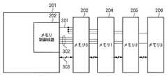
図2は、本実施の形態におけるメモリデバイスとメモリ制御回路を実装したLSIとの接続を示した概念図である。 FIG. 2 is a conceptual diagram showing the connection between the memory device and the LSI mounted with the memory control circuit in the present embodiment.
このシステムは、LSI201に実装されたメモリ制御回路202と、メモリデバイス0〜3(203〜206)とを有している。ここでLSI201に接続可能なメモリデバイスの数は最大4とする。メモリ制御回路202とメモリデバイス203〜206とは、アドレスやコマンド、チップセレクト信号等を伝送するコマンド信号群301と、ODT制御信号群302、データ、データストローブを転送するデータバス303により接続されている。 This system includes a
図3は、本実施の形態におけるメモリ制御回路202と、各メモリデバイス203〜206との間の信号接続を説明する図である。 FIG. 3 is a diagram for explaining signal connections between the
信号群301に含まれるバンクアドレスBA、アドレスA、行アドレスストローブRAS#、列アドレスストローブCAS#、ライトイネーブルWE#、データマスクDQM信号は、各メモリデバイス203〜206に対して共通に分配されている。一方、各メモリデバイスを選択するチップ選択信号CS0,CS1,CS2,CS3と、各メモリデバイスのODTを制御するODT制御信号302(ODT0,ODT1,ODT2,ODT3)は、各メモリデバイス203〜206に対して独立に接続されている。なお、ここで#は、負論理(ロウツルー)信号であることを示している。また、これらODT制御信号302は、メモリデバイス203〜206に対するODT制御信号に加えて、メモリ制御回路202が実装されるLSI201自身に対する制御信号(ODT)も含んでいる。尚、本実施の形態では、このLSI201自身に対するODT制御信号(ODT)の出力タイミングは、図4で示されるように、メモリデバイスでの制御タイミングと同様のタイミングとしている。しかし、メモリデバイスとLSIとで制御タイミングが異なる場合でも、それぞれ独立にタイミングを調整することで実現できることは言うまでも無い。これらの信号は、全てメモリ制御回路202から各メモリデバイス203〜206へ向かう単方向信号として実装される。The bank address BA, address A, row address strobe RAS #, column address strobe CAS #, write enable WE #, and data mask DQM signal included in the
更に、このメモリ制御回路202と各メモリデバイス203〜206間の双方向信号群としてデータバス303があり、これにはデータ信号DQとデータストローブ信号DQSが含まれている。 Further, there is a
メモリ制御回路202は、これら信号群を制御することにより、メモリデバイス203〜206との間でのデータ転送を可能にしている。 The
次に、図1を参照して、本実施の形態に係るメモリ制御回路202におけるODT制御について説明する。 Next, ODT control in the
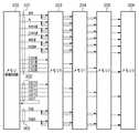
図1は、本実施の形態に係るメモリ制御回路202の構成を示すブロック図である。 FIG. 1 is a block diagram showing a configuration of the
本実施の形態に係るメモリ制御回路202は、メモリデータ制御部101、メモリコマンド制御部102、バスインターフェース回路103、ODT制御回路112を有している。 The
バスインターフェース回路103は、例えばCPU(不図示)等のバスマスタからのメモリアクセス要求を受取ると、アクセスするアドレス、リード/ライトの種別等をメモリコマンド制御部102へ転送する。またメモリデバイスに書き込むデータ、メモリデバイスから読み出したデータを、メモリデータ制御部101との間で送受信する。メモリデータ制御部101は、このバスインターフェース103とのデータの授受を行うとともに、メモリコマンド制御部102からのタイミング信号115に基づいて、メモリデバイスへのデータの送受信を実行する。 When receiving a memory access request from a bus master such as a CPU (not shown), for example, the
メモリコマンド制御部102は、バスインターフェース103から受信したメモリアクセス要求に含まれるアドレスと、リード/ライトの種別に基づいてメモリデバイスへのアクセスコマンドを作成する。また、メモリバス側のタイミング制御を行って信号群301を制御している。また、メモリコマンド制御部102は、自らが発行するメモリコマンドに応答して、データバス303上にデータがドライブされるタイミングを算出し、そのタイミングに応じてODT制御信号302の駆動を指示するODT許可信号110を発行する。このODT許可信号110は、各メモリデバイス203〜206に対して発行されるODT制御信号302が、データバス303上にデータが出力される間有効となるように制御される。ここで、データバス303へデータが出力される際、そのデータが有効となるtAOND(図4)前にODT制御信号がオン(ハイレベル)となる。そして、データバス303へのデータ出力が終了する際、そのデータバスのデータを無効にするタイミングのtAOFD前にODT制御信号がオフとなるように制御される。 The memory
こうして後述するように、ODT制御回路112で生成されるODT制御信号302は、フリップフロップ116を介して、ODT許可信号110の出力から最大1クロックサイクル遅延して出力される。従って、メモリコマンド制御部102から発行されるODT許可信号110は、データバス303のデータドライブに対して、tAONDとtAOFDのそれぞれに最大1サイクル加算したサイクル分先立ってハイレベルになるように制御されている。そしてメモリコマンド制御部102は、ODT許可信号110の発行と同時に、ODT方向信号109と、ODTデバイス信号108を発行する。ODT方向信号109は、データバス303にドライブされるデータのリード/ライトの種別を示し、ODTデバイス信号108は、データバス303にドライブされるデータのターゲットとなるメモリデバイスを示す。これらODTデバイス信号108、ODT方向信号109、ODT許可信号110は、ODT制御回路112に転送され、ODT制御回路112内で出力するODT制御信号302を決定する。尚、ODT方向信号109は、本実施の形態では、リード時はロウレベル、ライト時はハイレベルに設定されている。 Thus, as will be described later, the
以下、ODT制御回路112の構成と、その動作について説明する。 Hereinafter, the configuration and operation of the
ODT制御回路112は、ODT制御レジスタ104,105と、各メモリデバイスに対するODT制御信号302を生成するロジック回路を具備している。ここでODT制御レジスタ104は、メモリデバイスへのデータの書込み時におけるODTを制御するデータを記憶しており、ODT制御レジスタ105は、メモリデバイスからのデータの読出し時におけるODTを制御するデータを記憶している。 The
図5(A)は、ODT制御レジスタ104,105の構成を示す図である。尚、ここでODT制御レジスタ104,105は、各メモリデバイスとリード・ライトそれぞれ独立に設けられている。 FIG. 5A is a diagram illustrating the configuration of the ODT control registers 104 and 105. Here, the ODT control registers 104 and 105 are provided independently for each memory device and read / write.
本実施の形態では、最大4組のメモリデバイスの接続が可能であるため、4個のメモリデバイスに対してリード(読出し用)及びライト(書き込み用)それぞれのレジスタが設けられ、合計8個のODT制御レジスタが設けられている。 In this embodiment, since a maximum of four memory devices can be connected, a read (read) register and a write (write) register are provided for four memory devices, for a total of eight. An ODT control register is provided.
ODT制御レジスタのそれぞれは、図5(A)に示すように、接続される4つのメモリデバイス203〜206とLSI201自身に対応する5つのフィールドに分類されている。メモリデバイスに発行されるチップセレクト信号、及びリード/ライトの種別に応じて、どのODT制御信号をオンにするか否かが指定される。本実施の形態では、このフィールドに「1」が設定されている時(図5(B)参照)に、そのフィールドに対応するメモリデバイスに対するODT制御信号をオンにするものとする。 Each of the ODT control registers is classified into five fields corresponding to the four
図5(B)は、ODT制御レジスタ104,105の具体的な設定値の一例を示す図である。但し、これら設定値はあくまでも一例であって、メモリデバイスのメーカが推奨している仕様、或は、このLSI201、メモリデバイスを含むシステムの特性に応じた値に設定できることはもちろんである。 FIG. 5B is a diagram illustrating an example of specific setting values of the ODT control registers 104 and 105. However, these setting values are merely examples, and it is a matter of course that the setting values can be set according to the specifications recommended by the manufacturer of the memory device or the characteristics of the system including the
ここで、これら8個のODT制御レジスタから、実際にメモリアクセス時に使用するODT制御レジスタの選択は、メモリコマンド制御部102から発行されるODTデバイス信号108とODT方向信号109に基づいて行われる。本実施の形態では、セレクタ106によりメモリデバイスを選択し、セレクタ107によりリード/ライトの種別を選択することにより決定されるが、本発明はこの構成に限定されるものではない。 Here, from these eight ODT control registers, the ODT control register to be actually used at the time of memory access is selected based on the ODT device signal 108 and the ODT direction signal 109 issued from the memory
こうして選択されたODT制御レジスタの値は、AND回路111によりODT許可信号110と論理積が取られ、各メモリデバイス203〜206及びLSI201自身に対するODT制御信号302として出力される。 The value of the ODT control register thus selected is ANDed with the ODT permission signal 110 by the AND
図5(B)は、本実施の形態に係る制御レジスタの設定値の一例を示す図である。 FIG. 5B is a diagram illustrating an example of setting values of the control register according to the present embodiment.
図5(B)のように設定されると、メモリデバイス0(203)に対してデータの書込み要求(ライトアクセス)を発行する場合は、メモリデバイス1(204)に相当するODT制御信号のみがオンするように制御される。 When set as shown in FIG. 5B, when a data write request (write access) is issued to the memory device 0 (203), only the ODT control signal corresponding to the memory device 1 (204) is sent. Controlled to turn on.
またメモリデバイス1(204)に対してリードアクセスを発行する場合には、メモリデバイス0(CS0)、メモリデバイス2(CS2)、メモリデバイス3(CS3)、チップ自身に対するODT制御信号(OWN)をオンにするように制御される。即ち、メモリデバイス1(204)以外の全てのメモリデバイスのODT制御信号がオンになる。 When issuing a read access to the memory device 1 (204), the ODT control signal (OWN) for the memory device 0 (CS0), the memory device 2 (CS2), the memory device 3 (CS3), and the chip itself is sent. Controlled to turn on. That is, the ODT control signal of all memory devices other than the memory device 1 (204) is turned on.
また、メモリデバイス3(206)に対してデータの書込みを行う場合は、全てのフィールドに「0」が設定されているため、全てのODT制御信号をオフにするように制御される。 In addition, when data is written to the memory device 3 (206), all fields are set to “0”, so that all ODT control signals are controlled to be turned off.
図6は、図5(B)に示す設定値の下で、メモリデバイス2(205)のリードアクセスに続いて、メモリデバイス1(204)へライトアクセスが発行された場合の、ODT制御回路112に関連する信号とODT制御信号との関連を示す図である。 FIG. 6 shows an
図において、メモリデバイス2(205)のリードアクセス時には、601で示すODTリード制御レジスタ(CS2)の内容(10001)が選択されてセレクタ107から出力される。そしてODT許可信号110がハイレベルになった後の最初のクロック(CLK)の立上がりのタイミングT1で、フリップフロップ116からODT制御信号が出力される。この時のODT制御信号は、CS0とOWNに対応するODT0とODT_OWN信号のみがハイレベルとなった信号である。そして、ODT許可信号110がロウレベルになった後の最初のクロック(CLK)の立上がりのタイミングT2で、フリップフロップ116のラッチデータは「0」にリセットされて、ODT制御信号がロウレベルにリセットされる。In the figure, at the time of read access of the memory device 2 (205), the content (10001) of the ODT read control register (CS2) indicated by 601 is selected and output from the
次にメモリデバイス1(204)のライトアクセス時には、602で示すODTリード制御レジスタ(CS1)の内容(00110)が選択されてセレクタ107から出力される。そしてODT許可信号110がハイレベルになった後の最初のクロック(CLK)の立上がりのタイミングT3で、フリップフロップ116からODT制御信号が出力される。この時のODT制御信号は、CS2とCS3に対応するODT2とODT3のみがハイレベルとなった信号である。そして、ODT許可信号110がロウレベルになった後の最初のクロック(CLK)の立上がりのタイミングT4で、フリップフロップ116のラッチデータは「0」にリセットされて、ODT制御信号がロウレベルにリセットされる。 Next, at the time of write access of the memory device 1 (204), the content (00110) of the ODT read control register (CS1) indicated by 602 is selected and output from the
尚、本実施の形態では、メモリデバイスに対するODT制御信号302をハイレベル(有効)にする指定を、メモリ制御回路202のプログラマブルレジスタ104,105の設定値に従って決定している。 In the present embodiment, the designation of setting the
しかし本願発明はこれに限定されるものでなく、LSI201に外付けのメモリ素子に、これらODT制御レジスタ104,105と同様に各種設定値を記憶させて、その設定値を参照して上述の制御を行っても良い。 However, the present invention is not limited to this, and various setting values are stored in a memory element external to the
以上説明したように本実施の形態によれば、アクセス対象のメモリデバイスに対してODT制御信号302を有効にするメモリデバイスをプログラマブルに決定してODT制御を行うことができる。これにより、あるLSIのメモリアクセス制御や、メモリ動作速度が変更された場合、或は、このLSIを含むシステム、或は基板の構成が変更された場合であっても、的確なメモリデバイスのODT制御を実現することが可能となる。 As described above, according to the present embodiment, it is possible to perform ODT control by programmably determining a memory device that enables the
また、メモリデバイスとの間のデータ転送に影響を及ぼさない範囲で、不要なODT制御信号の発行を抑止することができるため、ODT時の電力消費を抑えることが可能となる。 In addition, since it is possible to suppress the issuance of unnecessary ODT control signals within a range that does not affect data transfer with the memory device, it is possible to suppress power consumption during ODT.
Claims (15)
Translated fromJapaneseメモリアクセス要求を解釈し、当該解釈に基づいて許可信号を発行するコマンド制御手段と、
前記コマンド制御手段による前記メモリアクセス要求の解釈に基づいて、前記複数のメモリデバイスの少なくとも1つに対してデータを送信または前記複数のメモリデバイスの少なくとも1つからデータを受信するデータ制御手段と、
前記コマンド制御手段からの許可信号に基づいて、前記複数のメモリデバイスの少なくとも1つへ保持手段を介してODT制御信号を発行するODT制御手段と、を有し、
前記コマンド制御手段は、前記メモリデバイスにおける信号反射を抑制するために前記データ制御手段と前記メモリデバイスとの間のデータの発生に対して少なくとも前記保持手段によって生じる遅延分先立って前記許可信号を発行することを特徴とするメモリ制御回路。A memory control circuit capable of connecting a plurality of memory devices having an on-die termination (ODT) mechanism,
Command control meansfor interpreting the memory access request and issuing a permission signalbased on the interpretation ;
Based on the memory access request interpretation by the command control unit, a data control means forreceiving data from at least one of saidplurality of memory at least one feed datatosignal or the plurality of memory devices in the device ,
ODT control means for issuing an ODT control signal to at least one of the plurality of memory devices via aholding meansbased on a permission signal from the command control means,
The command control means issues the permission signal at least in advance of a delaycaused by the holding means withrespect to the generation of data between the data control means and the memory device to suppress signal reflection in the memory device. A memory control circuit.
前記ODT制御手段は、前記記憶手段に記憶されている設定情報に基づいて、前記複数のメモリデバイスのそれぞれのODT機構を制御することを特徴とする請求項1に記載のメモリ制御回路。The memory control circuit according to claim 1, wherein the ODT control unit controls each ODT mechanism of the plurality of memory devices based on setting information stored in the storage unit.
前記ODT制御手段は、アクセス対象のメモリデバイスと、アクセスがリードであるかライトであるかに基づいて、前記複数のメモリデバイスのそれぞれのODT機構を制御することを特徴とする請求項1乃至5のいずれか1項に記載のメモリ制御回路。The command control meansfurther comprises command generation meansfor generating an access address and a read or write signal for the memory device based on an access request from a bus master,
The ODT control means, and the access target memory device, access is basedcrab is either aread-write,claim 1, wherein thecontroller controls the respectiveODT mechanism of the plurality of memory devicesThe memory control circuit accordingto any one of the above .
On-Die Termination(ODT)機構を有する複数のメモリデバイスと、
前記データバスを介して前記複数のメモリデバイスの少なくとも1つにデータを送信するデータ出力手段と、
メモリアクセス要求を解釈し、当該解釈に基づいて前記メモリデバイスのODT機構を有効にするための許可信号を発行するコマンド制御手段と、
前記コマンド制御手段からの許可信号に基づいて、前記複数のメモリデバイスの少なくとも1つに保持手段を介してODT制御信号を発行するODT制御手段と、を有し、
前記コマンド制御手段は、前記データ出力手段から前記メモリデバイスへデータが出力される間前記ODT機構が有効となるように、少なくとも前記保持手段によって生じる遅延分先立って前記許可信号を発行することを特徴とするメモリシステム。A data bus,
A plurality of memory devices having an on-die termination (ODT) mechanism;
And dataoutput means fortransmitting datato at least one of saidplurality of memory devicesthrough the data bus,
Command control meansfor interpreting a memory access request and issuing a permission signal for enabling the ODT mechanism of the memory devicebased on the interpretation ;
ODT control means for issuing an ODT control signal to at least one of the plurality of memory devices via aholding meansbased on a permission signal from the command control means,
The command control means issues the permission signal at least in advance of a delaycaused by the holding meansso that the ODT mechanism is valid while data is output from the data output means to the memory device. And memory system.
メモリアクセス要求を解釈し、当該解釈に基づいて許可信号を発行するコマンド制御工程と、
データ制御手段が、前記コマンド制御工程における前記メモリアクセス要求の解釈に基づいて、前記複数のメモリデバイスの少なくとも1つに対してデータを送信または前記複数のメモリデバイスの少なくとも1つからデータを受信するデータ制御工程と、
前記コマンド制御工程における許可信号に基づいて、前記複数のメモリデバイスの少なくとも1つに保持手段を介してODT制御信号を発行するODT制御工程と、を有し、
前記コマンド制御工程では、前記メモリデバイスにおける信号反射を抑制するために、前記データ制御手段と前記メモリデバイスとの間のデータの発生に対して少なくとも前記保持手段によって生じる遅延分先立って前記許可信号を発行することを特徴とするメモリ制御方法。A memory control method in a memory control circuit capable of connecting a plurality of memory devices having an on-die termination (ODT) mechanism,
A command control stepof interpreting the memory access request and issuing a permission signalbased on the interpretation ;
Data control means, on the basis of the interpretation of the memory access requests in the command control step,receiving data from at least one of transmission or the plurality of memory devices datato at least one of saidplurality of memory devices A data control process;
An ODT control step of issuing an ODT control signal to the at least one of the plurality of memory devices via aholding unitbased on a permission signal in the command control step,
In the command control step,in order to suppress signal reflection in the memory device, the permission signal is set in advance at leastby a delaycaused by the holding unit withrespect to generation of data between the data control unit and the memory device. A memory control method characterized by issuing.
前記コマンド制御手段は、前記データ出力手段から前記メモリデバイスへデータが出力される間前記ODT機構が有効となるように、少なくとも前記保持手段によって生じる遅延分先立って前記許可信号を発行することを特徴とするメモリ制御方法。The command control means issues the permission signal at least in advance of a delay caused by the holding means so that the ODT mechanism is valid while data is output from the data output means to the memory device. Memory control method.
Priority Applications (8)
| Application Number | Priority Date | Filing Date | Title |
|---|---|---|---|
| JP2006284142AJP5019573B2 (en) | 2006-10-18 | 2006-10-18 | Memory control circuit, memory system, memory control method thereof, and integrated circuit |
| EP12002246.2AEP2479676B1 (en) | 2006-10-18 | 2007-10-15 | Memory control circuit, memory control method, and integrated circuit |
| US12/441,139US8076954B2 (en) | 2006-10-18 | 2007-10-15 | Memory control circuit, memory control method, and integrated circuit |
| PCT/JP2007/070070WO2008047756A1 (en) | 2006-10-18 | 2007-10-15 | Memory control circuit, method, and integrated circuit |
| CN2007800389041ACN101529394B (en) | 2006-10-18 | 2007-10-15 | Memory control circuit, memory control method and integrated circuit |
| CN201310052387.0ACN103325420B (en) | 2006-10-18 | 2007-10-15 | Memory control device, memory control method and memory system |
| EP07829804AEP2075703A4 (en) | 2006-10-18 | 2007-10-15 | Memory control circuit, method, and integrated circuit |
| US13/294,107US8664972B2 (en) | 2006-10-18 | 2011-11-10 | Memory control circuit, memory control method, and integrated circuit |
Applications Claiming Priority (1)
| Application Number | Priority Date | Filing Date | Title |
|---|---|---|---|
| JP2006284142AJP5019573B2 (en) | 2006-10-18 | 2006-10-18 | Memory control circuit, memory system, memory control method thereof, and integrated circuit |
Publications (3)
| Publication Number | Publication Date |
|---|---|
| JP2008102706A JP2008102706A (en) | 2008-05-01 |
| JP2008102706A5 JP2008102706A5 (en) | 2011-12-22 |
| JP5019573B2true JP5019573B2 (en) | 2012-09-05 |
Family
ID=39313983
Family Applications (1)
| Application Number | Title | Priority Date | Filing Date |
|---|---|---|---|
| JP2006284142AExpired - Fee RelatedJP5019573B2 (en) | 2006-10-18 | 2006-10-18 | Memory control circuit, memory system, memory control method thereof, and integrated circuit |
Country Status (5)
| Country | Link |
|---|---|
| US (2) | US8076954B2 (en) |
| EP (2) | EP2075703A4 (en) |
| JP (1) | JP5019573B2 (en) |
| CN (2) | CN103325420B (en) |
| WO (1) | WO2008047756A1 (en) |
Families Citing this family (26)
| Publication number | Priority date | Publication date | Assignee | Title |
|---|---|---|---|---|
| US7486104B2 (en) | 2006-06-02 | 2009-02-03 | Rambus Inc. | Integrated circuit with graduated on-die termination |
| JP5430880B2 (en)* | 2008-06-04 | 2014-03-05 | ピーエスフォー ルクスコ エスエイアールエル | Memory module, method of using the same, and memory system |
| US8041865B2 (en)* | 2008-08-04 | 2011-10-18 | Qimonda Ag | Bus termination system and method |
| US7741867B2 (en)* | 2008-10-30 | 2010-06-22 | Hewlett-Packard Development Company, L.P. | Differential on-line termination |
| JP5344577B2 (en)* | 2009-02-19 | 2013-11-20 | エヌイーシーコンピュータテクノ株式会社 | Memory control apparatus and control method |
| JP4853554B2 (en)* | 2009-07-27 | 2012-01-11 | 株式会社ニコン | Digital camera |
| JP5346259B2 (en) | 2009-09-08 | 2013-11-20 | ルネサスエレクトロニクス株式会社 | Semiconductor integrated circuit |
| JP5390310B2 (en) | 2009-09-08 | 2014-01-15 | ルネサスエレクトロニクス株式会社 | Semiconductor integrated circuit |
| JP5363252B2 (en) | 2009-09-09 | 2013-12-11 | ルネサスエレクトロニクス株式会社 | Semiconductor integrated circuit |
| KR101688599B1 (en)* | 2010-06-01 | 2016-12-23 | 삼성전자 주식회사 | Mode conversion method, display driving Integrated Circuit and image processing system applying the method |
| US8274308B2 (en) | 2010-06-28 | 2012-09-25 | Intel Corporation | Method and apparatus for dynamic memory termination |
| US9153296B2 (en) | 2010-06-28 | 2015-10-06 | Intel Corporation | Methods and apparatuses for dynamic memory termination |
| US9239806B2 (en) | 2011-03-11 | 2016-01-19 | Micron Technology, Inc. | Systems, devices, memory controllers, and methods for controlling memory |
| CN103927286B (en)* | 2013-01-16 | 2018-05-15 | 森富科技股份有限公司 | memory structure for reducing reflection signal |
| KR102275812B1 (en) | 2015-09-04 | 2021-07-14 | 삼성전자주식회사 | Semiconductor memory device for improving signal integrity issue in center pad type of stacked chip structure |
| US10141935B2 (en)* | 2015-09-25 | 2018-11-27 | Intel Corporation | Programmable on-die termination timing in a multi-rank system |
| US20170255412A1 (en)* | 2016-03-04 | 2017-09-07 | Intel Corporation | Techniques for Command Based On Die Termination |
| KR20170112289A (en)* | 2016-03-31 | 2017-10-12 | 삼성전자주식회사 | Nonvolatile memory device, memory system including the same and method of operating nonvolatile memory device |
| KR102471160B1 (en)* | 2017-05-16 | 2022-11-25 | 삼성전자주식회사 | Nonvolatile memory including on-die-termination circuit and Storage device including the nonvolatile memory |
| US10340022B2 (en)* | 2017-05-16 | 2019-07-02 | Samsung Electronics Co., Ltd. | Nonvolatile memory including on-die-termination circuit and storage device including the nonvolatile memory |
| US10528515B2 (en)* | 2017-06-27 | 2020-01-07 | Intel Corporation | Memory channel driver with echo cancellation |
| KR102553266B1 (en)* | 2017-11-03 | 2023-07-07 | 삼성전자 주식회사 | Memory device including on-die-termination circuit |
| US10720197B2 (en) | 2017-11-21 | 2020-07-21 | Samsung Electronics Co., Ltd. | Memory device for supporting command bus training mode and method of operating the same |
| CN109101387A (en)* | 2018-08-15 | 2018-12-28 | 晶晨半导体(深圳)有限公司 | The adjustment method and system of DDR module |
| KR20210010691A (en) | 2019-07-17 | 2021-01-28 | 삼성전자주식회사 | Memory device and memory package |
| CN116820344B (en)* | 2023-07-03 | 2024-04-26 | 摩尔线程智能科技(北京)有限责任公司 | Memory access circuit and memory access method, integrated circuit and electronic device |
Family Cites Families (32)
| Publication number | Priority date | Publication date | Assignee | Title |
|---|---|---|---|---|
| US6347367B1 (en)* | 1999-01-29 | 2002-02-12 | International Business Machines Corp. | Data bus structure for use with multiple memory storage and driver receiver technologies and a method of operating such structures |
| JP4794059B2 (en)* | 2001-03-09 | 2011-10-12 | 富士通セミコンダクター株式会社 | Semiconductor device |
| JP3799251B2 (en)* | 2001-08-24 | 2006-07-19 | エルピーダメモリ株式会社 | Memory device and memory system |
| JP2003197753A (en)* | 2001-12-26 | 2003-07-11 | Elpida Memory Inc | Memory device and memory bus transmission system |
| KR100471162B1 (en)* | 2002-02-27 | 2005-03-08 | 삼성전자주식회사 | High speed memory system |
| KR100422451B1 (en)* | 2002-05-24 | 2004-03-11 | 삼성전자주식회사 | method for controlling on-die termination and control circuit therefore |
| CN100565490C (en) | 2002-11-20 | 2009-12-02 | 微米技术有限公司 | Active termination control through on-module registers |
| US7142461B2 (en)* | 2002-11-20 | 2006-11-28 | Micron Technology, Inc. | Active termination control though on module register |
| KR100541045B1 (en)* | 2003-05-13 | 2006-01-10 | 삼성전자주식회사 | Dual bank system, memory for use in this system, and on-die termination method of this memory |
| KR100604843B1 (en)* | 2004-03-26 | 2006-07-31 | 삼성전자주식회사 | Memory module having on-die termination circuit and its control method |
| US7516281B2 (en)* | 2004-05-25 | 2009-04-07 | Micron Technology, Inc. | On-die termination snooping for 2T applications in a memory system implementing non-self-terminating ODT schemes |
| US20050289287A1 (en)* | 2004-06-11 | 2005-12-29 | Seung-Man Shin | Method and apparatus for interfacing between test system and embedded memory on test mode setting operation |
| TWI249104B (en)* | 2004-06-23 | 2006-02-11 | Via Tech Inc | Control device, method, and system for accessing data from an external memory module |
| US7437497B2 (en)* | 2004-08-23 | 2008-10-14 | Apple Inc. | Method and apparatus for encoding memory control signals to reduce pin count |
| US7289383B2 (en)* | 2004-08-23 | 2007-10-30 | Apple Inc. | Reducing the number of power and ground pins required to drive address signals to memory modules |
| US7138823B2 (en)* | 2005-01-20 | 2006-11-21 | Micron Technology, Inc. | Apparatus and method for independent control of on-die termination for output buffers of a memory device |
| JP2006284142A (en) | 2005-04-04 | 2006-10-19 | Kubota Corp | Drying equipment |
| DE102005036528B4 (en)* | 2005-07-29 | 2012-01-26 | Qimonda Ag | Memory module and method for operating a memory module |
| US7560956B2 (en)* | 2005-08-03 | 2009-07-14 | Micron Technology, Inc. | Method and apparatus for selecting an operating mode based on a determination of the availability of internal clock signals |
| US7259585B2 (en)* | 2005-09-28 | 2007-08-21 | International Business Machines Corporation | Selective on-die termination for improved power management and thermal distribution |
| KR100805696B1 (en)* | 2005-09-29 | 2008-02-21 | 주식회사 하이닉스반도체 | Semiconductor memory device |
| US7372293B2 (en)* | 2005-12-07 | 2008-05-13 | Intel Corporation | Polarity driven dynamic on-die termination |
| US7414426B2 (en)* | 2005-12-07 | 2008-08-19 | Intel Corporation | Time multiplexed dynamic on-die termination |
| JP4857815B2 (en)* | 2006-02-28 | 2012-01-18 | 富士ゼロックス株式会社 | Memory system |
| JP4615461B2 (en)* | 2006-03-10 | 2011-01-19 | 京セラミタ株式会社 | Memory controller |
| US7486104B2 (en)* | 2006-06-02 | 2009-02-03 | Rambus Inc. | Integrated circuit with graduated on-die termination |
| KR100734320B1 (en)* | 2006-06-16 | 2007-07-02 | 삼성전자주식회사 | On-die termination control method of memory devices sharing signal line |
| JP4895183B2 (en)* | 2006-07-21 | 2012-03-14 | キヤノン株式会社 | Memory controller |
| US7755951B2 (en)* | 2006-09-01 | 2010-07-13 | Canon Kabushiki Kaisha | Data output apparatus, memory system, data output method, and data processing method |
| KR100866601B1 (en)* | 2006-12-04 | 2008-11-03 | 삼성전자주식회사 | Apparatus and method for controlling termination resistance of semiconductor device |
| US7843213B1 (en)* | 2009-05-21 | 2010-11-30 | Nanya Technology Corp. | Signal termination scheme for high speed memory modules |
| US8274308B2 (en)* | 2010-06-28 | 2012-09-25 | Intel Corporation | Method and apparatus for dynamic memory termination |
- 2006
- 2006-10-18JPJP2006284142Apatent/JP5019573B2/ennot_activeExpired - Fee Related
- 2007
- 2007-10-15WOPCT/JP2007/070070patent/WO2008047756A1/enactiveApplication Filing
- 2007-10-15CNCN201310052387.0Apatent/CN103325420B/ennot_activeExpired - Fee Related
- 2007-10-15EPEP07829804Apatent/EP2075703A4/ennot_activeWithdrawn
- 2007-10-15CNCN2007800389041Apatent/CN101529394B/ennot_activeExpired - Fee Related
- 2007-10-15EPEP12002246.2Apatent/EP2479676B1/ennot_activeCeased
- 2007-10-15USUS12/441,139patent/US8076954B2/ennot_activeExpired - Fee Related
- 2011
- 2011-11-10USUS13/294,107patent/US8664972B2/enactiveActive
Also Published As
| Publication number | Publication date |
|---|---|
| US20120060003A1 (en) | 2012-03-08 |
| WO2008047756A1 (en) | 2008-04-24 |
| EP2479676B1 (en) | 2016-01-13 |
| EP2479676A1 (en) | 2012-07-25 |
| CN101529394A (en) | 2009-09-09 |
| US8076954B2 (en) | 2011-12-13 |
| CN101529394B (en) | 2013-03-13 |
| EP2075703A4 (en) | 2009-12-02 |
| CN103325420A (en) | 2013-09-25 |
| US20090230989A1 (en) | 2009-09-17 |
| JP2008102706A (en) | 2008-05-01 |
| US8664972B2 (en) | 2014-03-04 |
| EP2075703A1 (en) | 2009-07-01 |
| CN103325420B (en) | 2016-07-13 |
Similar Documents
| Publication | Publication Date | Title |
|---|---|---|
| JP5019573B2 (en) | Memory control circuit, memory system, memory control method thereof, and integrated circuit | |
| US6981089B2 (en) | Memory bus termination with memory unit having termination control | |
| EP1668523B2 (en) | Integrated circuit with bi-modal data strobe | |
| JP4599409B2 (en) | Commands that control different processes on different chips | |
| US5721860A (en) | Memory controller for independently supporting synchronous and asynchronous DRAM memories | |
| KR100201057B1 (en) | Integrated circuit i/o using a high performance bus interface | |
| US7260691B2 (en) | Apparatus and method for initialization of a double-sided DIMM having at least one pair of mirrored pins | |
| CN111352881B (en) | Signal transmitting and receiving device, storage device and method of operating the same | |
| US6785189B2 (en) | Method and apparatus for improving noise immunity in a DDR SDRAM system | |
| US8289767B2 (en) | Providing a ready-busy signal from a non-volatile memory device to a memory controller | |
| JP4782830B2 (en) | Non-DRAM indicator and method for accessing data not stored in a DRAM array | |
| US7864604B2 (en) | Multiple address outputs for programming the memory register set differently for different DRAM devices | |
| JP5087886B2 (en) | Memory control device | |
| JP2010192031A (en) | Semiconductor memory device, memory module including the same, and data processing system | |
| JP2010192030A (en) | Semiconductor memory device, memory module including the same, and data processing system | |
| JP2006516059A (en) | Control of active termination via module registers | |
| CN111274162B (en) | Dual in-line memory module device of storage-level memory and data access method | |
| US20130314968A1 (en) | Offsetting clock package pins in a clamshell topology to improve signal integrity | |
| CN117195820A (en) | Design method and equipment of DDR (double data rate) expansion circuit in board-mounted memory mode | |
| TWI818436B (en) | memory system | |
| US12367943B2 (en) | Reference voltage adjustment per path for high speed memory signaling | |
| TWI830830B (en) | Signal transmitting and receiving apparatus, method of operating the same, memory device, and method of operating the same | |
| TWI715331B (en) | Control method of memory system |
Legal Events
| Date | Code | Title | Description |
|---|---|---|---|
| A521 | Request for written amendment filed | Free format text:JAPANESE INTERMEDIATE CODE: A523 Effective date:20091013 | |
| A621 | Written request for application examination | Free format text:JAPANESE INTERMEDIATE CODE: A621 Effective date:20091013 | |
| A521 | Request for written amendment filed | Free format text:JAPANESE INTERMEDIATE CODE: A523 Effective date:20111108 | |
| A131 | Notification of reasons for refusal | Free format text:JAPANESE INTERMEDIATE CODE: A131 Effective date:20120116 | |
| A521 | Request for written amendment filed | Free format text:JAPANESE INTERMEDIATE CODE: A523 Effective date:20120313 | |
| TRDD | Decision of grant or rejection written | ||
| A01 | Written decision to grant a patent or to grant a registration (utility model) | Free format text:JAPANESE INTERMEDIATE CODE: A01 Effective date:20120608 | |
| A01 | Written decision to grant a patent or to grant a registration (utility model) | Free format text:JAPANESE INTERMEDIATE CODE: A01 | |
| A61 | First payment of annual fees (during grant procedure) | Free format text:JAPANESE INTERMEDIATE CODE: A61 Effective date:20120611 | |
| R151 | Written notification of patent or utility model registration | Ref document number:5019573 Country of ref document:JP Free format text:JAPANESE INTERMEDIATE CODE: R151 | |
| FPAY | Renewal fee payment (event date is renewal date of database) | Free format text:PAYMENT UNTIL: 20150622 Year of fee payment:3 | |
| LAPS | Cancellation because of no payment of annual fees |