Movatterモバイル変換


[0]ホーム

URL:


JP5018565B2 - Micro contact printing method and micro contact printing apparatus - Google Patents

Micro contact printing method and micro contact printing apparatus
Download PDF

Info

Publication number
JP5018565B2
JP5018565B2JP2008055672AJP2008055672AJP5018565B2JP 5018565 B2JP5018565 B2JP 5018565B2JP 2008055672 AJP2008055672 AJP 2008055672AJP 2008055672 AJP2008055672 AJP 2008055672AJP 5018565 B2JP5018565 B2JP 5018565B2
Authority
JP
Japan
Prior art keywords
stamp
substrate
sample substrate
support
sample
Prior art date
Legal status (The legal status is an assumption and is not a legal conclusion. Google has not performed a legal analysis and makes no representation as to the accuracy of the status listed.)
Active
Application number
JP2008055672A
Other languages
Japanese (ja)
Other versions
JP2009208413A (en
Inventor
亮也 高橋
Current Assignee (The listed assignees may be inaccurate. Google has not performed a legal analysis and makes no representation or warranty as to the accuracy of the list.)
Brother Industries Ltd
Original Assignee
Brother Industries Ltd
Priority date (The priority date is an assumption and is not a legal conclusion. Google has not performed a legal analysis and makes no representation as to the accuracy of the date listed.)
Filing date
Publication date
Application filed by Brother Industries LtdfiledCriticalBrother Industries Ltd
Priority to JP2008055672ApriorityCriticalpatent/JP5018565B2/en
Publication of JP2009208413ApublicationCriticalpatent/JP2009208413A/en
Application grantedgrantedCritical
Publication of JP5018565B2publicationCriticalpatent/JP5018565B2/en
Activelegal-statusCriticalCurrent
Anticipated expirationlegal-statusCritical

Links

Images

Landscapes

Description

Translated fromJapanese

本発明は、マイクロコンタクトプリント方法、及びマイクロコンタクトプリント装置に関する。そしてより詳細には、試料基板上にスタンプを載置させ、スタンプの自重にてスタンプを試料基板に押圧させることによって、スタンプに付着する被覆膜の材料を試料基板に転写させるマイクロコンタクトプリント方法及びマイクロコンタクトプリント装置に関する。  The present invention relates to a microcontact printing method and a microcontact printing apparatus. More specifically, a microcontact printing method for transferring the material of the coating film adhering to the stamp to the sample substrate by placing the stamp on the sample substrate and pressing the stamp against the sample substrate by its own weight. And a microcontact printing apparatus.

マイクロコンタクトプリント法は、スタンプの微細な凹凸部表面に被覆膜の材料を付着させた状態で、スタンプを被転写基板に密着させることによって、パターン化した被覆膜を被転写基板の表面に形成させる方法である。本方法は、微細な被覆膜のパターンを安価に量産可能であるとして注目されており、実現に向けて研究がすすめられている。  In the microcontact printing method, a patterned coating film is applied to the surface of a substrate to be transferred by closely attaching the material of the coating film to the surface of the fine irregularities of the stamp, with the stamp closely attached to the substrate to be transferred. It is a method of forming. This method is attracting attention as it allows mass production of a fine coating film pattern at low cost, and research is being carried out toward its realization.

マイクロコンタクトプリント法では、例えば、被覆膜材料としてチオールや有機シランを使用し、試料基板に転写させることにより、試料基板に自己組織化有機単分子膜(Self Assembled Monolayer、以下「SAM」という。)が形成される。そして形成されたSAM最表面にある官能基を任意に選択することによって、試料基板上にさまざまな機能を付与した微細なパターンを形成させることが可能となる。  In the micro-contact printing method, for example, thiol or organosilane is used as a coating film material and transferred to a sample substrate, whereby the sample substrate is self-assembled organic monolayer (hereinafter referred to as “SAM”). ) Is formed. Then, by arbitrarily selecting a functional group on the formed SAM outermost surface, it is possible to form a fine pattern having various functions on the sample substrate.

マイクロコンタクトプリント法において被転写基板上に均一な被覆膜を形成させるためには、スタンプと被転写基板との並行度を高度に維持した状態で双方を密着させる必要があることが知られている。そして、高度に並行度を維持可能なマイクロコンタクトプリント装置として、被転写基板を固定するための第一ステーションが、X軸微粗動ダイヤルとY軸微粗動ダイヤルとを備えたX−Yステージからなるマイクロコンタクトプリント装置が提案されている(例えば、特許文献1参照)。このマイクロコンタクトプリント装置では、X軸微粗動ダイヤルとY軸微粗動ダイヤルとを調整することによってスタンプと被転写基板との並行度を高度に維持することが可能となっているため、スタンプと被転写体とを密着させてスタンプの凹凸部に付着する被覆膜の材料を被転写体に均一に転写させることが可能となっている。
特開2005−129791号公報
It is known that in order to form a uniform coating film on a substrate to be transferred in the micro contact printing method, it is necessary to closely adhere both of the stamp and the substrate to be transferred while maintaining a high degree of parallelism. Yes. As a microcontact printing apparatus capable of maintaining a high degree of parallelism, the first station for fixing the transfer substrate includes an X-Y coarse adjustment dial and a Y-axis fine adjustment dial. There has been proposed a microcontact printing apparatus (see, for example, Patent Document 1). In this microcontact printing apparatus, it is possible to maintain a high degree of parallelism between the stamp and the transfer substrate by adjusting the X-axis fine coarse movement dial and the Y-axis fine coarse movement dial. It is possible to uniformly transfer the material of the coating film adhering to the concavo-convex portion of the stamp to the transfer object by bringing the image and the transfer object into close contact with each other.
JP 2005-129791 A

しかしながら特許文献1に記載のマイクロコンタクトプリント装置では、スタンプと被転写基板との高度な並行度を実現するために複雑な制御機能を備える必要があり、装置が高コストとなってしまって、低コストなプロセスであるというマイクロコンタクトプリント法の利点を生かしきれないという問題点があった。  However, in the microcontact printing apparatus described inPatent Document 1, it is necessary to provide a complicated control function in order to realize a high degree of parallelism between the stamp and the transferred substrate, which increases the cost of the apparatus. There is a problem that the advantages of the microcontact printing method, which is a costly process, cannot be fully utilized.

本発明は上記課題を解決するためになされたものであり、低コストでスタンプと被転写基板との並行度を維持しつつ双方を密着させることが可能なマイクロコンタクトプリント装置、及びマイクロコンタクトプリント方法を提供することを目的とする。  The present invention has been made in order to solve the above-described problem, and a microcontact printing apparatus and a microcontact printing method capable of bringing the stamp and the substrate to be transferred into close contact with each other while maintaining parallelism at low cost. The purpose is to provide.

上記課題を解決するために、請求項1に係る発明のマイクロコンタクトプリント方法は、スタンプの表面に付着された被覆膜の材料を試料基板の表面に転写し、前記試料基板上に、所定パターンの被覆膜を形成するマイクロコンタクトプリント方法であって、前記試料基板の上方に配置されているスタンプであって下面に被覆膜の材料が付着されているスタンプの周縁部分を下方から接離可能に支持する支持体と、当該支持体に接離可能に支持された状態の当該スタンプの下方に配置されている前記試料基板を下方から固定した基板台とを上下方向に相対移動させ、当該スタンプと当該試料基板とを近接させる第一移動工程と、前記第一移動工程にて前記スタンプと前記試料基板とを近接させるように前記支持体と前記基板台とを相対移動させ、前記スタンプと前記試料基板とを接触させた後、さらに継続して前記支持体と前記基板台とを相対移動させることによって、前記支持体から前記スタンプを離隔させ、前記試料基板の上側に前記スタンプを載置させる載置工程と、前記載置工程において、前記試料基板上に前記スタンプが載置され、前記支持体から前記スタンプが離隔した後、当該スタンプの上方より当該スタンプに対して気体を放出することにより、当該試料基板に当該スタンプを押圧する圧力転写工程と、前記載置工程の後、前記支持体と前記基板台とを相対移動させることによって、前記試料基板から前記スタンプを離隔させる第二移動工程とを備え、前記載置工程により前記試料基板上に前記スタンプが載置された際に、当該スタンプの自重によって当該試料基板に当該スタンプが押圧され、当該スタンプに付着されている被覆膜の材料が前記試料基板に転写されることを特徴とする。In order to solve the above-described problem, the microcontact printing method according to the first aspect of the present invention transfers the coating film material attached to the surface of the stamp onto the surface of the sample substrate, and a predetermined pattern is formed on the sample substrate. A microcontact printing method for forming a coating film of the stamp, wherein the peripheral portion of the stamp, which is disposed above the sample substrate and has the coating film material attached to the lower surface, is contacted and separated from below. A support body that can be supported, and a substrate base that fixes the sample substrate disposed below the stamp in a state of being supported so as to be able to contact and separate from the support body, relative to each other in the vertical direction, A first moving step of bringing the stamp and the sample substrate close to each other; and the support and the substrate stage are relatively moved so that the stamp and the sample substrate are brought close to each other in the first moving step. Then, after the stamp and the sample substrate are brought into contact with each other, the stamper is separated from the support by continuously moving the support and the substrate base, and the stamp is placed on the upper side of the sample substrate. In the placing step of placing the stamp and the placing stepdescribed above, after the stamp is placed on the sample substrate and the stamp is separated from the support, a gas is applied to the stamp from above the stamp. The stamp is separated from the sample substrate by relatively moving the support and the substrate table afterthe pressure transfer step of pressing the stamp against the sample substrate and the placingstep. A second moving step, and when the stamp is placed on the sample substrate by the placing step, the sample base is caused by its own weight. The stamp is pressed, the material of the coating film is attached to the stamp, characterized in that it is transferred to the sample substrate.

また、請求項に係る発明のマイクロコンタクトプリント装置は、スタンプの表面に付着された被覆膜の材料を試料基板の表面に転写し、前記試料基板上に、所定パターンの被覆膜を形成するためのマイクロコンタクトプリント装置であって、下面に被覆膜の材料が付着された前記スタンプの周縁部分を下方から接離可能に支持する支持体と、前記支持体に支持された状態の前記スタンプの下方に前記試料基板を配置するために、当該試料基板を下方から固定する基板台と、前記スタンプが前記支持体に支持されている状態の当該支持体と前記試料基板が前記基板台に固定されている状態の当該基板台とを上下方向に相対移動させ、当該スタンプと当該試料基板とを近接させる第一移動手段と、前記第一移動手段により前記スタンプと前記試料基板とを近接させるように前記支持体と前記基板台とを相対移動させ、前記スタンプと前記試料基板とを接触させた後、さらに継続して前記支持体と前記基板台とを相対移動させ、前記試料基板の上側に前記スタンプを載置させることによって、前記支持体から前記スタンプが離隔した場合において、前記支持体から前記スタンプが離隔した状態を検出する離隔状態検出手段と、前記離隔状態検出手段により前記支持体から前記スタンプが隔離したことを検出した後、前記支持体と前記基板台とを相対移動させることによって、前記試料基板から前記スタンプを離隔させる第二移動手段とを備え、前記第一移動手段により前記試料基板上に前記スタンプが載置された際、当該スタンプの自重によって当該試料基板に当該スタンプが押圧され、当該スタンプに付着されている被覆膜の材料が前記試料基板に転写されることを特徴とする。According to asecond aspect of the present invention, there is provided a microcontact printing apparatus for transferring a coating film material attached to a surface of a stamp onto a surface of a sample substrate, and forming a coating film having a predetermined pattern on the sample substrate. And a support that supports a peripheral portion of the stamp having a coating film material attached to a lower surface thereof so as to be able to contact and separate from below, and the support that is supported by the support. In order to dispose the sample substrate below the stamp, a substrate stand for fixing the sample substrate from below, and the support and the sample substrate in a state where the stamp is supported by the support are attached to the substrate stand. A first moving means for relatively moving the substrate table in a fixed state in the vertical direction to bring the stamp and the sample substrate close to each other, and the stamp and the sample by the first moving means. Relative movement of the support and the substrate stage so as to bring the substrate close to each other, contact the stamp and the sample substrate, and then continue the relative movement of the support and the substrate stage, A separation state detection means for detecting a state in which the stamp is separated from the support when the stamp is separated from the support by placing the stamp on the upper side of the sample substrate, and the separation state detection A second moving means for separating the stamp from the sample substrate by relatively moving the support and the substrate base after detecting that the stamp is separated from the support by means, When the stamp is placed on the sample substrate by the first moving means, the stamp is pressed against the sample substrate by its own weight. Wherein the material of the coating film is attached to the stamp is transferred to the sample substrate.

また、請求項に係る発明のマイクロコンタクトプリント装置は、請求項に記載の発明の構成に加えて、前記スタンプの上方より当該スタンプに対して気体を放出する気体放出手段をさらに備え、前記離隔状態検出手段において前記支持体から前記スタンプが離隔したことを検出した場合に、前記気体放出手段により前記スタンプに対して気体を放出し、前記試料基板に当該スタンプを押圧することを特徴とする。Furthermore, microcontact printing apparatus of the invention according toclaim3, in addition to the configuration of the invention according toclaim2, further comprising a gas release means for releasing the gas with respect to the stamp from above of the stamp, the When the separation state detecting means detects that the stamp is separated from the support, the gas releasing means releases gas to the stamp and presses the stamp against the sample substrate. .

また、請求項に係る発明のマイクロコンタクトプリント装置は、請求項またはに記載の発明の構成に加えて、前記試料基板を下方から固定する前記基板台において、前記試料基板の下面と接する少なくとも上面部分が柔軟材料によって構成されている。According to afourth aspect of the present invention, in addition to the configuration of thesecond orthird aspect of the invention, the microcontact printing apparatus is in contact with the lower surface of the sample substrate in the substrate stand for fixing the sample substrate from below. At least the upper surface portion is made of a flexible material.

また、請求項に係る発明のマイクロコンタクトプリント装置は、請求項またはに記載の発明の構成に加えて、前記試料基板を下方から固定する前記基板台において、前記試料基板の下面と接する少なくとも上面部分が硬質材料によって構成されていると共に、その下側部分を柔軟材料によって構成されている。According to afifth aspect of the present invention, in addition to the configuration of thesecond orthird aspect of the invention, the microcontact printing apparatus is in contact with the lower surface of the sample substrate in the substrate stand for fixing the sample substrate from below. At least the upper surface portion is made of a hard material, and the lower portion thereof is made of a flexible material.

また、請求項に係る発明のマイクロコンタクトプリント装置は、請求項またはに記載の発明の構成に加えて、前記試料基板を下方から固定する前記基板台の上面を弾性的に支持する弾性支持手段を備えている。According to asixth aspect of the present invention, in addition to the configuration of thesecond orthird aspect of the invention, the microcontact printing apparatus elastically supports the upper surface of the substrate base for fixing the sample substrate from below. Support means are provided.

請求項1に係る発明のマイクロコンタクトプリント方法では、試料基板上にスタンプを置き、スタンプの自重によって、試料基板にスタンプを押圧させてスタンプ上の被覆膜の材料を試料基板に転写させる。このことによって、複雑な制御を行うことなく、容易にスタンプと試料基板とを平行に配置させ、均一にスタンプ上の被覆膜の材料を転写させることが可能となる。またマイクロコンタクトプリント方法では、スタンプの自重による押圧に加えて、気体圧力によってスタンプと試料基板とを押圧させる。このことによって、自重では不足する押圧の圧力を補充することが可能となる。In the microcontact printing method according to the first aspect of the present invention, a stamp is placed on the sample substrate, and the stamp substrate is pressed against the sample substrate by the weight of the stamp so that the material of the coating film on the stamp is transferred to the sample substrate. Accordingly, it is possible to easily arrange the stamp and the sample substrate in parallel without performing complicated control, and to uniformly transfer the material of the coating film on the stamp.In the microcontact printing method, the stamp and the sample substrate are pressed by a gas pressure in addition to the pressing due to the weight of the stamp. This makes it possible to replenish the pressing pressure that is insufficient under its own weight.

また、請求項に係る発明のマイクロコンタクトプリント装置では、試料基板上にスタンプを置き、スタンプの自重によって、スタンプと試料基板とを押圧させてスタンプ上の被覆膜の材料を試料基板に転写させることが可能となる。このことによって、複雑な制御を行うことなく、容易にスタンプと試料基板とを平行に配置させ、均一にスタンプ上の被覆膜の材料を転写させることが可能となる。In the microcontact printing apparatus of the invention according toclaim2 , a stamp is placed on the sample substrate, and the stamp and the sample substrate are pressed by the dead weight of the stamp to transfer the material of the coating film on the stamp to the sample substrate. It becomes possible to make it. Accordingly, it is possible to easily arrange the stamp and the sample substrate in parallel without performing complicated control, and to uniformly transfer the material of the coating film on the stamp.

また、請求項に係る発明のマイクロコンタクトプリント装置では、スタンプの自重によるスタンプと試料基板との押圧に加えて、気体圧力によってスタンプと試料基板とを押圧させる。このことによって、請求項に記載の発明の効果に加えて、自重では不足する押圧の圧力を補充することが可能となる。In the microcontact printing apparatus according to thethird aspect of the invention, the stamp and the sample substrate are pressed by gas pressure in addition to the pressing of the stamp and the sample substrate by the weight of the stamp. Thus, in addition to the effect of the invention described inclaim2 , it becomes possible to replenish the pressure of the press that is insufficient under the own weight.

また、請求項に係る発明のマイクロコンタクトプリント装置では、請求項またはに記載の発明の効果に加えて、基板台を固定させないことで、試料基板がスタンプと接触するときに局所的な圧力集中を分散させ、均一にスタンプ上の被覆膜の材料を転写させることが可能となる。Moreover, in the microcontact printing apparatus of the invention according toclaim4 , in addition to the effect of the invention ofclaim2 or3 , by not fixing the substrate stand, when the sample substrate comes into contact with the stamp, It is possible to disperse the pressure concentration and uniformly transfer the coating film material on the stamp.

また、請求項に係る発明のマイクロコンタクトプリント装置では、請求項またはに記載の発明の効果に加えて、基板台を固定させないことで、試料基板がスタンプと接触するときに局所的な圧力集中を分散させ、均一にスタンプ上の被覆膜の材料を転写させることが可能となる。In addition, in the microcontact printing apparatus of the invention according toclaim5 , in addition to the effect of the invention ofclaim2 or3 , by not fixing the substrate stand, when the sample substrate comes into contact with the stamp, It is possible to disperse the pressure concentration and uniformly transfer the coating film material on the stamp.

また、請求項に係る発明のマイクロコンタクトプリント装置では、請求項またはに記載の発明の効果に加えて、基板台を固定させないことで、試料基板がスタンプと接触するときに局所的な圧力集中を分散させ、均一にスタンプ上の被覆膜の材料を転写させることが可能となる。In addition, in the microcontact printing apparatus of the invention according toclaim6 , in addition to the effect of the invention ofclaim2 or3 , by not fixing the substrate stand, when the sample substrate comes into contact with the stamp, It is possible to disperse the pressure concentration and uniformly transfer the coating film material on the stamp.

以下、本発明を具現化したマイクロコンタクトプリント装置100、及びマイクロコンタクトプリント装置100を使用したマイクロコンタクトプリント方法について、図面を参照して説明する。なお以下の図面は、本発明が採用しうる技術的特徴を説明するために用いられるものであり、記載されている装置の構成、各種処理のフローチャートなどは、特に特定的な記載がない限り、それのみに限定する趣旨ではなく、単なる説明例である。  Hereinafter, amicrocontact printing apparatus 100 embodying the present invention and a microcontact printing method using themicrocontact printing apparatus 100 will be described with reference to the drawings. The following drawings are used to explain the technical features that can be adopted by the present invention, and the configuration of the apparatus described, the flowchart of various processes, etc., unless otherwise specified, It is not intended to be limited to that, but merely an illustrative example.

本発明のマイクロコンタクトプリント装置100は、マイクロコンタクトプリント法を実現するための装置である。本装置では、スタンプ2(及びスタンプホルダー1)(図2参照)を試料基板3(図1参照)上に載置させ、スタンプ2(及びスタンプホルダー1)の自重によってスタンプ2を試料基板3に押圧させることにより、スタンプ2表面の微細な凹凸部に付着する被覆膜材料を試料基板3に転写させる。  Themicrocontact printing apparatus 100 of the present invention is an apparatus for realizing a microcontact printing method. In this apparatus, the stamp 2 (and the stamp holder 1) (see FIG. 2) is placed on the sample substrate 3 (see FIG. 1), and thestamp 2 is placed on thesample substrate 3 by the dead weight of the stamp 2 (and the stamp holder 1). By pressing, the coating film material adhering to the fine irregularities on the surface of thestamp 2 is transferred to thesample substrate 3.

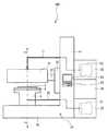
はじめに、図1及び図2を参照して、マイクロコンタクトプリント装置100について説明する。図1は、マイクロコンタクトプリント装置100の物理的構成を示す側面図であり、図2は、スタンパー31及び基板台5の図1中A−A線における矢視方向断面図である。なお、図1における左側をマイクロコンタクトプリント装置100の前方、図1における右側をマイクロコンタクトプリント装置100の後方、図1における紙面手前側をマイクロコンタクトプリント装置100の右方、図1における紙面手奥行き側をマイクロコンタクトプリント装置100の左方とする。  First, themicrocontact printing apparatus 100 will be described with reference to FIGS. 1 and 2. FIG. 1 is a side view showing the physical configuration of themicrocontact printing apparatus 100, and FIG. 2 is a cross-sectional view taken along the line AA in FIG. 1 is the front side of themicrocontact printing apparatus 100, the right side of FIG. 1 is the rear side of themicrocontact printing apparatus 100, the front side of the paper in FIG. 1 is the right side of themicrocontact printing apparatus 100, and the depth of the paper surface in FIG. The side is the left side of themicrocontact printing apparatus 100.

はじめに、図1を参照して、マイクロコンタクトプリント装置100の物理的構成について説明する。図1に示すように、マイクロコンタクトプリント装置100は、水平方向に配置されたベッド部40と、当該ベッド部40の後方端部より垂直方向に立設された脚柱部41とから構成される、側面視逆L字形状のベース34を備えている。  First, the physical configuration of themicrocontact printing apparatus 100 will be described with reference to FIG. As shown in FIG. 1, themicrocontact printing apparatus 100 includes abed portion 40 arranged in a horizontal direction and apedestal column portion 41 erected in a vertical direction from a rear end portion of thebed portion 40. Thebase 34 is provided with an L-shaped base 34 in a side view.

そして、ベース34におけるベッド部40の上側には、マイクロコンタクトプリント装置100により被覆膜材料を転写させる試料基板3を配置するための基板台5が配置されている。基板台5は、その上面に水平面部を備えた側面視略T字形状を有している。また、当該水平面部の上側には基板サポートステージ4が配置されており、被覆膜材料の転写処理が実施される場合には、当該基板サポートステージ4の上側に試料基板3が配置される。また、基板台5の右側面には吸入ホース20の一端側が接続され、当該吸入ホース20の他端側がベース34の脚柱部41の前側面に接続されている。  Asubstrate stage 5 for arranging thesample substrate 3 on which the coating film material is transferred by the microcontact printing apparatus 100 is arranged above thebed portion 40 in thebase 34. Thesubstrate base 5 has a substantially T shape in side view with a horizontal surface portion on the upper surface thereof. Further, thesubstrate support stage 4 is disposed above the horizontal plane portion, and thesample substrate 3 is disposed above thesubstrate support stage 4 when the coating film material transfer process is performed. Further, one end side of thesuction hose 20 is connected to the right side surface of thesubstrate base 5, and the other end side of thesuction hose 20 is connected to the front side surface of thepedestal 41 of thebase 34.

基板台5は、上方からスタンプ2(図2参照)が試料基板3に対して押圧される場合において、試料基板3を下方から支持するために設けられている。また、基板サポートステージ4は、上側に配置される試料基板3を基板台5に密着させるために設けられている。基板サポートステージ4を構成する材料としては、試料基板3との親和性が良好で試料基板3を密着させ易く、且つ、柔軟性を備えた材料が使用される。このことによって、試料基板3自体が反りや凹凸を有する場合であっても、基板台5に密着させることが可能となる。さらに、試料基板3自体が反りを有していることにより生じるスタンプ2押圧時の圧力集中を、試料基板3全体に均一に分散させることができ、良好に被覆膜材料を試料基板3に転写させることが可能となる。基板サポートステージ4の材料としては、例えば、ゴム、スポンジ、PDMS(Polydimethysiloxane)が挙げられる。  Thesubstrate stand 5 is provided to support thesample substrate 3 from below when the stamp 2 (see FIG. 2) is pressed against thesample substrate 3 from above. Further, thesubstrate support stage 4 is provided in order to bring thesample substrate 3 disposed on the upper side into close contact with the substrate table 5. As a material constituting thesubstrate support stage 4, a material having good affinity with thesample substrate 3, easy adhesion of thesample substrate 3, and flexibility is used. As a result, even when thesample substrate 3 itself has warpage or unevenness, it can be brought into close contact with the substrate table 5. Furthermore, the pressure concentration when thestamp 2 is pressed due to the warping of thesample substrate 3 itself can be uniformly distributed over theentire sample substrate 3, and the coating film material can be satisfactorily transferred to thesample substrate 3. It becomes possible to make it. Examples of the material for thesubstrate support stage 4 include rubber, sponge, and PDMS (Polydimethylsiloxane).

吸入ホース20は、試料基板3と基板サポートステージ4との隙間からエアを吸入するためのホースであり、試料基板3と基板サポートステージ4との隙間の圧力を減圧させることによって、試料基板3を基板サポートステージ4に吸着させている(詳細は後述する。)。吸入ホース20は、ベース34の脚柱部41の内部を経由してバキュームポンプ61(後述)に接続されている。  Thesuction hose 20 is a hose for sucking air from the gap between thesample substrate 3 and thesubstrate support stage 4, and the pressure in the gap between thesample substrate 3 and thesubstrate support stage 4 is reduced to remove thesample substrate 3. It is adsorbed on the substrate support stage 4 (details will be described later). Thesuction hose 20 is connected to a vacuum pump 61 (described later) via the inside of thepedestal 41 of thebase 34.

また、ベース34の脚柱部41の前側面にはスライダ33が配置され、スライダ33より前方水平方向にスタンパーアーム32が延設され、さらにスタンパーアーム32の前端部には直方体形状のスタンパー31が接続されている。スタンパー31の平面視形状は基板台5の平面視形状よりも大きくなるように設定されている。また、スタンパー31は、スタンパーアーム32に支持された状態で基板台5の上方に配置されている。また、スタンパー31の上側には、エア等の気体を注入する気体注入ホース11が接続されており、気体注入ホース11におけるスタンパー31と接続する側と反対側の端部は、ベース34の脚柱部41の前側に接続された状態となっている。  Further, aslider 33 is disposed on the front side surface of thepedestal 41 of thebase 34, astamper arm 32 extends in front of theslider 33 in the horizontal direction, and arectangular parallelepiped stamper 31 is provided at the front end of thestamper arm 32. It is connected. The plan view shape of thestamper 31 is set to be larger than the plan view shape of the substrate table 5. Thestamper 31 is disposed above the substrate table 5 while being supported by thestamper arm 32. Agas injection hose 11 for injecting a gas such as air is connected to the upper side of thestamper 31, and the end of thegas injection hose 11 opposite to the side connected to thestamper 31 is a pedestal of thebase 34. It is connected to the front side of theportion 41.

スライダ33は、延設されたスタンパーアーム32及びスタンパー31を三次元方向に駆動可能な駆動機構を備えている。駆動機構は、コントロールボックス36(後述)に内蔵されている制御基板50(図3参照)に設けられたCPU51(図3参照)からの指示に基づいて、スタンパーアーム32及びスタンパー31を移動させる。  Theslider 33 includes a drive mechanism that can drive theextended stamper arm 32 andstamper 31 in a three-dimensional direction. The drive mechanism moves thestamper arm 32 and thestamper 31 based on an instruction from a CPU 51 (see FIG. 3) provided on a control board 50 (see FIG. 3) built in a control box 36 (described later).

スタンパー31の内部には、試料基板3に被覆膜材料を転写するためのスタンプ2(図2参照)が配置されている(詳細は後述する。)。  A stamp 2 (see FIG. 2) for transferring the coating film material to thesample substrate 3 is disposed inside the stamper 31 (details will be described later).

気体注入ホース11は、加圧孔9(図2参照)を介してスタンパー31内部の空間部分(以下、「加圧室15」という。(図2参照))に向けて気体を放出することにより、スタンプ2(図2参照)が試料基板3に押圧される場合の圧力を補填するために設けられている。気体注入ホース11は、ベース34の脚柱部41の内部を経由してコンプレッサ62に接続されている。  Thegas injection hose 11 discharges gas toward the space portion inside the stamper 31 (hereinafter referred to as “pressurizingchamber 15” (see FIG. 2)) through the pressurizing hole 9 (see FIG. 2). The stamp 2 (see FIG. 2) is provided to compensate for the pressure when thesample substrate 3 is pressed. Thegas injection hose 11 is connected to thecompressor 62 via the inside of thepedestal 41 of thebase 34.

また、ベース34の脚柱部41の右方側面には、表示装置63と入力装置56とが夫々設けられている。表示装置63には、マイクロコンタクトプリント装置100の駆動状態が表示されるとともに、CCDカメラ13(図2参照)にて観察された画像が表示される。表示される画像は、オペレータによるスタンパー31の位置合わせの際に使用される。また、入力装置56は、レバーやボタン、スイッチ等から構成されている。そして、オペレータが入力装置56を操作することにより、マイクロコンタクトプリント装置100の電源制御、各種設定、及び各種駆動制御を行うことが可能となっている。  Further, adisplay device 63 and aninput device 56 are provided on the right side surface of thepedestal 41 of thebase 34, respectively. On thedisplay device 63, the driving state of themicrocontact printing apparatus 100 is displayed, and an image observed by the CCD camera 13 (see FIG. 2) is displayed. The displayed image is used when the operator aligns thestamper 31. Theinput device 56 includes a lever, a button, a switch, and the like. When the operator operates theinput device 56, it is possible to perform power control, various settings, and various drive controls of themicrocontact printing apparatus 100.

また、ベース34の脚柱部41の後側面には、バキュームポンプ61を内部に備えたバキュームポンプ格納筺体37、制御基板50(図3参照)を内部に備えたコントロールボックス36、及び、コンプレッサ62を内部に備えたコンプレッサ格納筺体35が、夫々配置されている。  Further, on the rear side surface of thepedestal 41 of thebase 34, avacuum pump housing 37 having avacuum pump 61 therein, acontrol box 36 having a control board 50 (see FIG. 3) inside, and acompressor 62 are provided. Are respectively disposed in thecompressor housings 35.

これらのうち、バキュームポンプ格納筺体37の内部に配置されているバキュームポンプ61は、吸入ホース20と接続されており、吸入ホース20を介して気体を吸入する。このことにより、試料基板3と基板サポートステージ4との隙間を減圧し、試料基板3を基板サポートステージ4に吸着させることが可能となっている。また、コンプレッサ格納筺体35の内部に配置されているコンプレッサ62は、気体注入ホース11と接続されており、気体注入ホース11を介して気体を放出する。このことにより、スタンプホルダー1(図2参照)に向けて気体を放出してスタンプ2を試料基板3に押圧させることが可能となっている。また、コントロールボックス36には、マイクロコンタクトプリント装置100の制御処理を司る制御基板50(図3参照)が内蔵されている。そして制御基板50が備えるCPU51(図3参照)により、スライダ33、バキュームポンプ61、及びコンプレッサ62の制御、入力装置56を介した入力操作の監視、CCDカメラ13(図2参照)の観察画像の表示装置63への表示、圧力センサスイッチ6(図2参照)の圧力検出等の処理を実行している(図3参照、後述)。  Among these, thevacuum pump 61 disposed inside thevacuum pump housing 37 is connected to thesuction hose 20 and sucks gas through thesuction hose 20. As a result, the gap between thesample substrate 3 and thesubstrate support stage 4 can be decompressed, and thesample substrate 3 can be adsorbed to thesubstrate support stage 4. Further, thecompressor 62 disposed inside thecompressor housing 35 is connected to thegas injection hose 11 and discharges gas through thegas injection hose 11. Thus, it is possible to release the gas toward the stamp holder 1 (see FIG. 2) and press thestamp 2 against thesample substrate 3. Thecontrol box 36 incorporates a control board 50 (see FIG. 3) that controls the control processing of themicrocontact printing apparatus 100. Then, the CPU 51 (see FIG. 3) provided in thecontrol board 50 controls theslider 33, thevacuum pump 61, and thecompressor 62, monitors the input operation via theinput device 56, and displays the observation image of the CCD camera 13 (see FIG. 2). Processing such as display on thedisplay device 63 and pressure detection of the pressure sensor switch 6 (see FIG. 2) is executed (see FIG. 3 and described later).

次に、図2を参照して、基板台5及びスタンパー31の物理的構成について説明する。はじめに、基板台5について説明する。基板台5は、その上面に水平部分を備えた正面視略T字形状を有しており、水平部分の上側には、柔軟性を有する基板サポートステージ4が配置されている。また、基板台5には吸入通路19が内設されている。吸入通路19はその中間部分において3方向に分岐した形状を有しており、一端部は基板台5の右側面において吸入ホース20に接続され、その他の端部は、基板サポートステージ4を貫通して孔部(「基板吸着孔17」という。)が表出された状態となっている。従って、この状態でバキュームポンプ61(図1参照)を駆動させて基板吸着孔17から気体を吸入し、基板サポートステージ4と試料基板3との隙間の圧力を減圧させることによって、試料基板3を基板台5に吸着させることが可能となっている。  Next, with reference to FIG. 2, the physical structure of the board |substrate stand 5 and thestamper 31 is demonstrated. First, thesubstrate stand 5 will be described. Thesubstrate stand 5 has a substantially T-shape in front view with a horizontal portion on the upper surface, and a flexiblesubstrate support stage 4 is disposed above the horizontal portion. Asuction passage 19 is provided in the substrate table 5. Thesuction passage 19 has a shape branched in three directions at an intermediate portion thereof, one end is connected to thesuction hose 20 on the right side surface of thesubstrate base 5, and the other end penetrates thesubstrate support stage 4. The hole (referred to as “substrate suction hole 17”) is exposed. Accordingly, in this state, the vacuum pump 61 (see FIG. 1) is driven to suck the gas from thesubstrate suction hole 17, and the pressure in the gap between thesubstrate support stage 4 and thesample substrate 3 is reduced, whereby thesample substrate 3 is removed. It can be adsorbed to the substrate table 5.

次いで、スタンパー31について説明する。スタンパー31は、被覆膜材料が凹凸部に付着されたスタンプ2を備えている。そして、上方からスタンプ2を試料基板3に押圧して被覆膜材料を転写させるために、基板台5の上方に配置される。スタンパー31は、スタンプ2を下面に接着させた状態の透明のスタンプホルダー1と、スタンプホルダー1を下方から接離可能に支持するスタンパー枠7と、スタンプホルダー1とスタンパー枠7との接触部分に設けられた圧力センサスイッチ6と、加圧室15の圧力を制御するための開閉式圧力調整弁8と、気体注入ホース11からの気体を加圧室15に放出するための加圧孔9と、スタンプホルダー1を透してスタンプ2及び下方の試料基板3を観察するためのCCDカメラ13とを備えている。  Next, thestamper 31 will be described. Thestamper 31 includes astamp 2 in which a coating film material is attached to the uneven portion. In order to transfer the coating film material by pressing thestamp 2 against thesample substrate 3 from above, it is disposed above the substrate table 5. Thestamper 31 includes atransparent stamp holder 1 in a state where thestamp 2 is bonded to the lower surface, astamper frame 7 that supports thestamp holder 1 so that thestamp holder 1 can be contacted and separated from below, and a contact portion between thestamp holder 1 and thestamper frame 7. Apressure sensor switch 6 provided; an open / closepressure regulating valve 8 for controlling the pressure in the pressurizingchamber 15; and apressurizing hole 9 for releasing the gas from thegas injection hose 11 to the pressurizingchamber 15. And aCCD camera 13 for observing thestamp 2 and thelower sample substrate 3 through thestamp holder 1.

スタンパー31は、平面視正方形状を有している。そして図2に示すように、水平部7aと、水平部の周縁部より下方鉛直方向に延設された鉛直部7bと、鉛直部7bの下端部よりスタンパー31の内方に延設された支持部7cとから構成されるスタンパー枠7を備えている。スタンパー枠7は、下面に開口部を備えた略直方体形状となっており、鉛直部7bの後側においてスタンパーアーム32(図1参照)と接続されている。そして、支持部7cにおいて、スタンプホルダー1を下方から接離可能に支持している。  Thestamper 31 has a square shape in plan view. And as shown in FIG. 2, thehorizontal part 7a, thevertical part 7b extended in the vertical direction below the peripheral part of the horizontal part, and the support extended inward of thestamper 31 from the lower end part of thevertical part 7bA stamper frame 7 composed of aportion 7c is provided. Thestamper frame 7 has a substantially rectangular parallelepiped shape with an opening on the lower surface, and is connected to the stamper arm 32 (see FIG. 1) on the rear side of thevertical portion 7b. Thesupport portion 7c supports thestamp holder 1 so as to be able to contact and separate from below.

スタンプホルダー1は、鉛直部7bの内接面の平面視形状と同じ平面視形状を有している。そして、外力が加わっていない状態では、支持部7cに下方から接離可能に支持されている。また、スタンプホルダー1に対して上方に押力が加えられた場合に、支持部7cと離隔して鉛直部7bの内接面に沿い上下方に移動する。なお、スタンパー枠7とスタンプホルダー1とに囲まれることにより、加圧室15は気密な状態となっている。さらに、スタンプホルダー1の下面には、被覆膜材料が付着される凹凸面を下方に向けた状態でスタンプ2が接着されている。  Thestamp holder 1 has the same planar view shape as the planar view shape of the inscribed surface of thevertical portion 7b. In a state where no external force is applied, thesupport portion 7c is supported so as to be able to contact and separate from below. Further, when a pressing force is applied to thestamp holder 1 upward, thestamp holder 1 moves upward and downward along the inscribed surface of thevertical portion 7b apart from thesupport portion 7c. The pressurizingchamber 15 is airtight by being surrounded by thestamper frame 7 and thestamp holder 1. Further, thestamp 2 is bonded to the lower surface of thestamp holder 1 with the uneven surface to which the coating film material is attached facing downward.

スタンプ2及びスタンプホルダー1の重量は、スタンプ2及びスタンプホルダー1を試料基板3上に載置させ、これらの自重によりスタンプ2を試料基板3に押圧させる場合に最適な圧力が加わるように、あらかじめ調整されている。また、水平部7aに配置されたCCDカメラ13(後述)により、スタンプホルダー1を透してスタンプ2及び試料基板3を観察可能とするために、スタンプホルダー1は透明な材料にて形成されている。また、スタンプ2が試料基板3に押圧される場合において、スタンプ2の凹凸の形成状態が不均一であると、スタンプ2に均一に圧力が印加されず良好に被覆膜材料が転写されない可能性がある。このことを防止するために、スタンプホルダー1は、柔軟性のある材料にて形成されていてもよい。スタンプホルダー1を構成する材料としては、透過率の高い公知の材料が使用される。例えば、ガラス、プラスチックが挙げられる。また、柔軟性のある材料が使用されても構わない。例えばPDMSが挙げられる。  The weight of thestamp 2 and thestamp holder 1 is set in advance so that an optimum pressure is applied when thestamp 2 and thestamp holder 1 are placed on thesample substrate 3 and thestamp 2 is pressed against thesample substrate 3 by their own weight. It has been adjusted. Thestamp holder 1 is made of a transparent material so that thestamp 2 and thesample substrate 3 can be observed through thestamp holder 1 by a CCD camera 13 (described later) disposed in thehorizontal portion 7a. Yes. Further, when thestamp 2 is pressed against thesample substrate 3, if the unevenness of thestamp 2 is not uniform, pressure may not be uniformly applied to thestamp 2 and the coating film material may not be transferred well. There is. In order to prevent this, thestamp holder 1 may be formed of a flexible material. As a material constituting thestamp holder 1, a known material having a high transmittance is used. Examples thereof include glass and plastic. Further, a flexible material may be used. An example is PDMS.

支持部7cの上面に設けられている圧力センサスイッチ6は、スタンプホルダー1と支持部7cとの接離状態を検出するために設けられている。そして、スタンプホルダー1が支持部7cと接触し、支持部7cがスタンプホルダー1を支持しているか、又は、スタンプホルダー1が支持部7cと接触しておらず、支持部7cがスタンプホルダー1を支持していないかを検出する。  Thepressure sensor switch 6 provided on the upper surface of thesupport portion 7c is provided to detect the contact / separation state between thestamp holder 1 and thesupport portion 7c. Thestamp holder 1 is in contact with thesupport portion 7c, and thesupport portion 7c is supporting thestamp holder 1, or thestamp holder 1 is not in contact with thesupport portion 7c, and thesupport portion 7c is Detect if not supported.

また、鉛直部7bには、開閉式圧力調整弁8が設けられている。開閉式圧力調整弁8は、加圧室15の圧力を調整するために設けられている。そして、加圧室15の圧力が所定値以上になった場合に、弁を開放して圧力を下げる。このように、開閉式圧力調整弁8にて加圧室15の圧力が所定値以下なるように調整することによって、スタンプホルダー1に過度な力が働いてしまうことを防止している。  In addition, an open / closepressure regulating valve 8 is provided in thevertical portion 7b. The open / closepressure adjusting valve 8 is provided to adjust the pressure in the pressurizingchamber 15. Then, when the pressure in the pressurizingchamber 15 becomes a predetermined value or more, the valve is opened to lower the pressure. In this way, by adjusting the pressure in the pressurizingchamber 15 to be equal to or lower than the predetermined value by the open / closepressure regulating valve 8, it is possible to prevent an excessive force from acting on thestamp holder 1.

また、水平部7aには、CCDカメラ13と加圧孔9とが設けられている。そして、水平部7aの平面視正方形状の中心側に下方を観察可能な状態でCCDカメラ13が複数設けられており、CCDカメラ13の外側に下方に気体を放出可能な状態で加圧孔9が複数設けられている。  Thehorizontal portion 7a is provided with aCCD camera 13 and apressure hole 9. A plurality ofCCD cameras 13 are provided at the center side of the square shape in plan view of thehorizontal portion 7a so that the lower side can be observed, and the pressure holes 9 are provided outside theCCD camera 13 so that gas can be discharged downward. Are provided.

CCDカメラ13は、被覆膜材料の転写処理(図4、図5参照)が実施される前に、スタンプ2と試料基板3との位置関係を確認するために設けられている。スタンプ2はスタンプホルダー1の下面の任意の部分に接着させることが可能であり、試料基板3は基板サポートステージ4上面の任意の部分に吸着させることが可能となっている。従って、双方が固定される位置によっては、スタンパー31を下方に移動させた場合に、スタンプ2と試料基板3とが所望の位置関係で接触しない状況が発生しうる。そこでこのような状況を防止するために、被覆膜材料の転写処理の前にあらかじめCCDカメラ13にてスタンプホルダー1を透してスタンプ2と試料基板3とを観察し、観察画像を表示装置63(図1参照)に表示させる。オペレータは、表示装置63に表示されている観察画像を確認し、スタンプ2と試料基板3とが所望の位置関係に配置されていない場合には、入力装置56(図1参照)を操作してスライダ33(図1参照)を駆動させ、スタンパー31を前後左右方向に移動させる。そして、スタンプ2と試料基板3とが所望の位置関係に配置されるように、スタンパー31の位置を調整する。このことによって、確実に試料基板3にスタンプ2が所望の位置関係で接触して押圧され、スタンプ2に付着する被覆膜材料が試料基板3に転写される。  TheCCD camera 13 is provided to confirm the positional relationship between thestamp 2 and thesample substrate 3 before the coating film material transfer process (see FIGS. 4 and 5) is performed. Thestamp 2 can be adhered to an arbitrary portion on the lower surface of thestamp holder 1, and thesample substrate 3 can be adsorbed to an arbitrary portion on the upper surface of thesubstrate support stage 4. Therefore, depending on the position where both are fixed, there may occur a situation where thestamp 2 and thesample substrate 3 do not contact with each other when thestamper 31 is moved downward. Therefore, in order to prevent such a situation, thestamp 2 and thesample substrate 3 are observed through thestamp holder 1 in advance by theCCD camera 13 before the coating film material is transferred, and the observation image is displayed on the display device. 63 (see FIG. 1). The operator checks the observation image displayed on thedisplay device 63, and operates the input device 56 (see FIG. 1) when thestamp 2 and thesample substrate 3 are not arranged in a desired positional relationship. The slider 33 (see FIG. 1) is driven to move thestamper 31 in the front-rear and left-right directions. Then, the position of thestamper 31 is adjusted so that thestamp 2 and thesample substrate 3 are arranged in a desired positional relationship. This ensures that thestamp 2 is brought into contact with and pressed against thesample substrate 3 in a desired positional relationship, and the coating film material adhering to thestamp 2 is transferred to thesample substrate 3.

加圧孔9は、スタンパー31の上側に接続されている気体注入ホース11を介してコンプレッサ62(図1参照)より放出される気体をスタンプホルダー1(図2参照)に向けて放出するために、孔を加圧室15に向けた状態で配置されている。このことによって、スタンプ2を試料基板3に押圧させる力を補填し、スタンプ2に付着されている被覆膜材料を良好に試料基板3に転写させる。  The pressurizinghole 9 discharges the gas released from the compressor 62 (see FIG. 1) toward the stamp holder 1 (see FIG. 2) via thegas injection hose 11 connected to the upper side of thestamper 31. The holes are arranged in a state where the holes are directed to the pressurizingchamber 15. As a result, the force for pressing thestamp 2 against thesample substrate 3 is compensated, and the coating film material attached to thestamp 2 is transferred to thesample substrate 3 satisfactorily.

以上説明したように、マイクロコンタクトプリント装置100は、外力が加わっていない状態では、スタンプ2とスタンプホルダー1とがスタンパー枠7により下方から接離可能に支持された状態となっている。そして、被覆膜材料の転写処理時においては、スライダ33が制御され、スタンパー31が下方に移動することによって、試料基板3にスタンプ2とスタンプホルダー1とが載置され、スタンプ2及びスタンプホルダー1に対してスタンパー枠7がさらに下方に移動することにより、そのスタンパー枠7がスタンプホルダー1から離隔する。この状態で、スタンプ2とスタンプホルダー1との自重によりスタンプ2が試料基板3に押圧される。このことによって、スタンプ2と試料基板3とを平行に配置した状態で、被覆膜材料を試料基板3に転写させることが可能となる。また、スタンプ2が試料基板3に押圧されている状態で、加圧孔9よりスタンプホルダー1に向けて気体を放出し、スタンプ2を試料基板3に押し付ける。このことによって、スタンプ2及びスタンプホルダー1の自重では押圧する力が不足するような場合であっても、押圧する力を補填することが可能となり、良好に被覆膜材料を試料基板3に転写させることが可能となる。  As described above, themicrocontact printing apparatus 100 is in a state in which thestamp 2 and thestamp holder 1 are supported by thestamper frame 7 so as to be able to contact and separate from below when no external force is applied. When the coating film material is transferred, theslider 33 is controlled, and thestamper 31 moves downward, whereby thestamp 2 and thestamp holder 1 are placed on thesample substrate 3, and thestamp 2 and the stamp holder are placed. When thestamper frame 7 moves further downward relative to 1, thestamper frame 7 is separated from thestamp holder 1. In this state, thestamp 2 is pressed against thesample substrate 3 by the weight of thestamp 2 and thestamp holder 1. This makes it possible to transfer the coating film material to thesample substrate 3 in a state where thestamp 2 and thesample substrate 3 are arranged in parallel. Further, in a state where thestamp 2 is pressed against thesample substrate 3, gas is released from thepressure hole 9 toward thestamp holder 1, and thestamp 2 is pressed against thesample substrate 3. As a result, even if the pressing force of thestamp 2 and thestamp holder 1 is insufficient, the pressing force can be compensated, and the coating film material can be satisfactorily transferred to thesample substrate 3. It becomes possible to make it.

さらに、基板サポートステージ4は、柔軟性のある材料にて形成されている。このことによって、試料基板3にスタンプ2が押圧される場合において、局所的に圧力が印加されてしまう場合に、基板サポートステージ4が撓むことにより圧力集中を分散させることが可能となる。このことによって、スタンプ2を均一に試料基板3に押圧させることが可能となり、良好に被覆膜材料を試料基板3に転写させることが可能となる。  Further, thesubstrate support stage 4 is formed of a flexible material. As a result, when thestamp 2 is pressed against thesample substrate 3 and the pressure is locally applied, the pressure concentration can be dispersed by thesubstrate support stage 4 being bent. As a result, thestamp 2 can be uniformly pressed against thesample substrate 3, and the coating film material can be transferred to thesample substrate 3 satisfactorily.

次いで、コントロールボックス36(図1参照)内に備えられている制御基板50の電気的構成について、図3を参照して説明する。図3は、制御基板50の電気的構成を示すブロック図である。  Next, the electrical configuration of thecontrol board 50 provided in the control box 36 (see FIG. 1) will be described with reference to FIG. FIG. 3 is a block diagram showing an electrical configuration of thecontrol board 50.

制御基板50には、図3に示すように、マイクロコンタクトプリント装置100(図1参照)の制御処理を司るCPU51が設けられている。また、CPU51が制御処理を実行するために必要なプログラムやパラメータを記憶する不揮発性記憶素子であるROM52と、CPU51がプログラムに基づいて処理を実行する場合に発生する一時的なデータを記憶する揮発性記憶素子であるRAM53とが夫々設けられている。そして、CPU51がROM52及びRAM53のデータを読み出し、また必要に応じてRAM53にデータを記憶させることが可能なように、双方はバスを介して電気的に接続した状態となっている。また、CPU51にて実行される時間監視処理を可能とするためのタイマ58が設けられている。そして、CPU51に対して所定の周期信号を出力することが可能なように、タイマ58はCPU51と電気的に接続された状態となっている。  As shown in FIG. 3, thecontrol board 50 is provided with aCPU 51 that performs control processing of the microcontact printing apparatus 100 (see FIG. 1). In addition, aROM 52 that is a non-volatile storage element that stores programs and parameters necessary for theCPU 51 to execute control processing, and a volatile memory that stores temporary data generated when theCPU 51 executes processing based on the program. Each of theRAMs 53 is a volatile memory element. Then, both are electrically connected via a bus so that theCPU 51 can read the data in theROM 52 and theRAM 53 and store the data in theRAM 53 as necessary. In addition, atimer 58 for enabling time monitoring processing executed by theCPU 51 is provided. Thetimer 58 is electrically connected to theCPU 51 so that a predetermined periodic signal can be output to theCPU 51.

また、制御基板50には、バキュームポンプ61を駆動させるための駆動回路71と、コンプレッサ62を駆動させるための駆動回路72と、表示装置63を駆動させるための駆動回路73と、スライダ33を駆動させるための駆動回路74とが設けられており、CPU51による制御が可能なように、夫々の駆動回路とCPU51とが電気的に接続した状態となっている。駆動回路71は、バキュームポンプ61の気体吸入駆動の制御を実行することが可能な回路であり、バキュームポンプ61と電気的に接続されている。また、駆動回路72は、コンプレッサ62の気体放出駆動の制御を実行することが可能な回路であり、コンプレッサ62と電気的に接続されている。また、駆動回路73は、表示装置63にマイクロコンタクトプリント装置100の駆動状態を通知するための情報や、CCDカメラ13にて観察された画像等を表示させることが可能な回路であり、表示装置63と電気的に接続されている。また、駆動回路74は、スライダ33を制御してスタンパーアーム32及びスタンパー31を三次元方向に駆動させることが可能な回路であり、スライダ33と電気的に接続されている。  Thecontrol board 50 also drives adrive circuit 71 for driving thevacuum pump 61, adrive circuit 72 for driving thecompressor 62, adrive circuit 73 for driving thedisplay device 63, and theslider 33. Thedrive circuit 74 is provided so that the respective drive circuits and theCPU 51 are electrically connected so that the control by theCPU 51 is possible. Thedrive circuit 71 is a circuit capable of executing control of gas suction drive of thevacuum pump 61, and is electrically connected to thevacuum pump 61. Thedrive circuit 72 is a circuit capable of executing control of gas discharge drive of thecompressor 62, and is electrically connected to thecompressor 62. Thedrive circuit 73 is a circuit that can display information for notifying thedisplay device 63 of the drive state of themicrocontact printing apparatus 100, an image observed by theCCD camera 13, and the like. 63 is electrically connected. Thedrive circuit 74 is a circuit that can drive thestamper arm 32 and thestamper 31 in a three-dimensional direction by controlling theslider 33, and is electrically connected to theslider 33.

また、制御基板50に設けられているCPU51には、支持部7c(図2参照)に設けられている圧力センサスイッチ6が接続されており、圧力センサスイッチ6とスタンプホルダー1との接触の有無を検知可能な状態となっている。そして、CPU51は、圧力センサスイッチ6とスタンプホルダー1とが接触している場合に、支持部7cがスタンプホルダー1を支持した状態であると判断し、圧力センサスイッチ6とスタンプホルダー1とが接触していない場合に、支持部7cとスタンプホルダー1とが離隔し、スタンプ2(及びスタンプホルダー1)が試料基板3に載置した状態であると判断している。  Further, theCPU 51 provided on thecontrol board 50 is connected to thepressure sensor switch 6 provided on thesupport portion 7c (see FIG. 2), and whether or not thepressure sensor switch 6 and thestamp holder 1 are in contact with each other. Can be detected. Then, when thepressure sensor switch 6 and thestamp holder 1 are in contact, theCPU 51 determines that thesupport portion 7c is in a state of supporting thestamp holder 1, and thepressure sensor switch 6 and thestamp holder 1 are in contact with each other. If not, it is determined that thesupport portion 7c and thestamp holder 1 are separated from each other and the stamp 2 (and the stamp holder 1) is placed on thesample substrate 3.

また、制御基板50に設けられているCPU51には、水平部7a(図2参照)に設けられているCCDカメラ13が接続されており、CCDカメラ13により観察された画像のデータを受信することが可能な状態となっている。なお、受信した画像のデータは駆動回路73を介して表示装置63に表示させている。また、ベース34の脚柱部41(図1参照)の右方側面に設けられている入力装置56が接続されており、入力装置56を介した入力操作の監視をすることが可能な状態となっている。  TheCPU 51 provided on thecontrol board 50 is connected to theCCD camera 13 provided on thehorizontal portion 7a (see FIG. 2), and receives image data observed by theCCD camera 13. Is possible. The received image data is displayed on thedisplay device 63 via thedrive circuit 73. Further, aninput device 56 provided on the right side surface of the pedestal 41 (see FIG. 1) of thebase 34 is connected, and the input operation via theinput device 56 can be monitored. It has become.

次いで、マイクロコンタクトプリント装置100(図1参照)が備えるCPU51により実行される被覆膜材料の転写処理について、図4及び図5のフローチャートを参照して説明する。図4及び図5は、マイクロコンタクトプリント装置100のCPU51により実行される被覆膜材料の転写処理のフローチャートを示している。なお、図4及び図5に示す処理を実行させるプログラムはROM52に記憶されており、CPU51はこのプログラムを読み込んで処理を実行する。また、図4及び図5に示す処理は、オペレータにより入力装置56を介して入力が行われ、マイクロコンタクトプリント装置100による被腹膜材料の転写処理の実行指示がなされた場合に起動される。  Next, the coating film material transfer process executed by theCPU 51 provided in the microcontact printing apparatus 100 (see FIG. 1) will be described with reference to the flowcharts of FIGS. 4 and 5 show a flowchart of the coating film material transfer process executed by theCPU 51 of themicrocontact printing apparatus 100. FIG. A program for executing the processing shown in FIGS. 4 and 5 is stored in theROM 52, and theCPU 51 reads this program and executes the processing. 4 and 5 is started when an input is performed by the operator via theinput device 56 and themicrocontact printing apparatus 100 issues an instruction to execute the peritoneal material transfer process.

図4に示すように、転写処理が起動されると、はじめに、CPU51は、オペレータによるスタンパー31の位置調整が可能なように、CCDカメラ13による観察処理を開始する。そして得られる観察画像データを表示装置63に表示させる(S10)。  As shown in FIG. 4, when the transfer process is started, first, theCPU 51 starts the observation process by theCCD camera 13 so that the operator can adjust the position of thestamper 31. The obtained observation image data is displayed on the display device 63 (S10).

次いで、スタンプ2が配置されていない場合には、オペレータによりスタンプ2がスタンプホルダー1に接着され固定される。また、スタンプ2の凹凸面には被覆膜の材料が付着された状態となっている。ここで、試料基板3が基板台5上に配置されていない場合には、オペレータにより試料基板3が配置される。そして、試料基板3が基板サポートステージ4に配置された旨の入力操作が入力装置56(図1参照)を介してなされた場合には、CPU51は、駆動回路71を制御してバキュームポンプ61を駆動させ、試料基板3と基板サポートステージ4との隙間を減圧して試料基板3を吸着させる(S11)。  Next, when thestamp 2 is not arranged, thestamp 2 is adhered and fixed to thestamp holder 1 by the operator. Further, the material of the coating film is attached to the uneven surface of thestamp 2. Here, when thesample substrate 3 is not arranged on thesubstrate stand 5, thesample substrate 3 is arranged by the operator. When an input operation indicating that thesample substrate 3 is placed on thesubstrate support stage 4 is performed via the input device 56 (see FIG. 1), theCPU 51 controls thedrive circuit 71 to switch thevacuum pump 61 on. Driven to depressurize the gap between thesample substrate 3 and thesubstrate support stage 4 to adsorb the sample substrate 3 (S11).

次いで、表示装置63に表示されるCCDカメラ13の観察画像として、スタンプ2と試料基板3とが映し出され、オペレータによりスタンプ2と試料基板3との位置関係が確認される。ここで、スタンプ2と試料基板3とが所望の位置関係に配置されていない状態となっている場合には、オペレータにより入力装置56を介しスタンパー31を移動させるための入力操作が実施される。  Next, thestamp 2 and thesample substrate 3 are displayed as an observation image of theCCD camera 13 displayed on thedisplay device 63, and the positional relationship between thestamp 2 and thesample substrate 3 is confirmed by the operator. Here, when thestamp 2 and thesample substrate 3 are not arranged in a desired positional relationship, an input operation for moving thestamper 31 via theinput device 56 is performed by the operator.

そこでCPU51は、入力装置56よりスタンパー31を移動させるための入力操作が実行されたことを検出した場合には(S12:YES)、入力操作に応じ、駆動回路74を制御してスライダ33を駆動させ、スタンパー31を前後左右方向に移動させる(S14)。このことによって、スタンプ2の真下に試料基板3が配置される。そしてS13の処理に移行する。一方、スタンプ2と試料基板3とが所望の位置関係に配置されている場合には、入力装置56よりスタンパー31を移動させるための入力操作は行われないため(S12:NO)、そのままS13の処理に移行する。  Therefore, when theCPU 51 detects that an input operation for moving thestamper 31 from theinput device 56 is executed (S12: YES), theCPU 51 controls thedrive circuit 74 to drive theslider 33 according to the input operation. Thestamper 31 is moved in the front-rear and left-right directions (S14). As a result, thesample substrate 3 is disposed directly below thestamp 2. Then, the process proceeds to S13. On the other hand, when thestamp 2 and thesample substrate 3 are arranged in a desired positional relationship, an input operation for moving thestamper 31 from theinput device 56 is not performed (S12: NO). Transition to processing.

S13においては、CPU51は、オペレータにより転写処理の開始指示がなされたかどうかを判断する(S13)。何ら入力操作が実行されず、転写処理の開始指示がなされない場合には(S13:NO)、S12に戻り、継続して入力装置56よりスタンパー31を移動させるための入力操作を監視する(S12)。一方、オペレータにより入力装置56が操作され、転写処理の開始指示が選択された場合(S13:YES)、スタンプ2の直下に試料基板3が位置する状態となっていると判断して、転写処理を開始する。  In S13, theCPU 51 determines whether or not the operator has instructed to start the transfer process (S13). If no input operation is executed and no transfer processing start instruction is issued (S13: NO), the process returns to S12, and the input operation for continuously moving thestamper 31 from theinput device 56 is monitored (S12). ). On the other hand, when theinput device 56 is operated by the operator and an instruction to start the transfer process is selected (S13: YES), it is determined that thesample substrate 3 is positioned immediately below thestamp 2, and the transfer process is performed. To start.

オペレータにより転写処理の開始指示が選択されると、CPU51は、駆動回路74を制御してスライダ33を駆動させ、スタンパー31を下方に移動させる(以下、スタンパー31を下方に移動させる工程を「第一移動工程」という。)。このことによって、支持部7cに接離可能に支持されているスタンプホルダー1に接着されているスタンプ2と試料基板3とが徐々に接近し、そして双方は接触する。  When an instruction to start the transfer process is selected by the operator, theCPU 51 controls thedrive circuit 74 to drive theslider 33 to move thestamper 31 downward (hereinafter, the step of moving thestamper 31 downward is referred to as “first step”. One moving process ”). As a result, thestamp 2 bonded to thestamp holder 1 supported so as to be able to come in contact with and away from thesupport portion 7c and thesample substrate 3 gradually approach each other, and both come into contact with each other.

第一移動工程においてスタンパー31が下方に移動され、スタンプ2と試料基板3とが接触した状態で、CPU51は、さらに駆動回路74を制御してスライダ33を駆動させ、スタンパー31をさらに下方に移動させる(S15)。スタンプ2が接着したスタンプホルダー1は、支持部7cに接離可能に下方から支持された状態であるため、スタンパー31がさらに下方に移動することにより、スタンプホルダー1及びスタンプ2は試料基板3の上面に載置され、スタンプホルダー1は支持部7cから離隔した状態となる。そしてこの状態で、スタンプホルダー1及びスタンプ2の自重によりスタンプ2が試料基板3に押圧される。このことにより、スタンプ2に付着している被覆膜材料が試料基板3に転写される。  In the first movement step, thestamper 31 is moved downward, and thestamp 2 and thesample substrate 3 are in contact with each other, theCPU 51 further controls thedrive circuit 74 to drive theslider 33 and moves thestamper 31 further downward. (S15). Since thestamp holder 1 to which thestamp 2 is bonded is supported from below so as to be able to come into contact with and separate from thesupport portion 7c, thestamp holder 31 moves further downward, so that thestamp holder 1 and thestamp 2 are attached to thesample substrate 3. Thestamp holder 1 is placed on the upper surface and is separated from thesupport portion 7c. In this state, thestamp 2 is pressed against thesample substrate 3 by the weight of thestamp holder 1 and thestamp 2. As a result, the coating film material adhering to thestamp 2 is transferred to thesample substrate 3.

CPU51は、第一移動工程の過程で、支持部7cに配置されている圧力センサスイッチ6の状態を常時監視している(S17:NO)。そして、スタンプホルダー1及びスタンプ2が試料基板3の上面に載置した状態となることにより、支持部7cからスタンプホルダー1が離隔する。CPU51は圧力センサスイッチ6を介して離隔状態を検出し(S17:YES)、スタンプホルダー1及びスタンプ2が試料基板3に載置されたと判断する(以下、スタンプホルダー1及びスタンプ2を試料基板3上に載置させる工程を「載置工程」という。)。  TheCPU 51 constantly monitors the state of thepressure sensor switch 6 disposed on thesupport portion 7c during the first movement process (S17: NO). Then, when thestamp holder 1 and thestamp 2 are placed on the upper surface of thesample substrate 3, thestamp holder 1 is separated from thesupport portion 7c. TheCPU 51 detects the separation state via the pressure sensor switch 6 (S17: YES), and determines that thestamp holder 1 and thestamp 2 are placed on the sample substrate 3 (hereinafter, thestamp holder 1 and thestamp 2 are referred to as the sample substrate 3). The process of placing on top is referred to as the “placement process”).

載置工程においてスタンプホルダー1及びスタンプ2が試料基板3に載置された場合、次いでCPU51は、駆動回路72を制御してコンプレッサ62を駆動させ、気体注入ホース11を介して加圧孔9より加圧室15内に気体を放出させる(S19)。気体が放出されることにより、スタンプホルダー1が下方に押し下げられる。このことによって、さらにスタンプ2が試料基板3に押圧され、スタンプ2に付着した被覆膜材料が試料基板3に転写される(以下、気体を放出してスタンプ2を試料基板3に押圧させる工程を「圧力転写工程」という。)。  When thestamp holder 1 and thestamp 2 are placed on thesample substrate 3 in the placement step, theCPU 51 then controls thedrive circuit 72 to drive thecompressor 62 and from thepressure hole 9 via thegas injection hose 11. Gas is discharged into the pressurizing chamber 15 (S19). By releasing the gas, thestamp holder 1 is pushed downward. As a result, thestamp 2 is further pressed against thesample substrate 3, and the coating film material adhering to thestamp 2 is transferred to the sample substrate 3 (hereinafter, a step of releasing the gas and pressing thestamp 2 against the sample substrate 3). Is referred to as a “pressure transfer process”).

CPU51は、圧力転写工程において加圧孔9より気体を放出し、スタンプ2を試料基板3に押圧させた後、駆動回路74を制御してスライダ33の下方移動を停止させる(S21)。次いでCPU51は、図5に示すように、S19において気体を放出したタイミングからの経過時間を監視する(S23)。そして、所定の時間が経過するまで継続して駆動回路72を制御してコンプレッサ62を駆動させる。このことにより、継続して気体注入ホース11を介して加圧孔9よりスタンプホルダー1に向けて気体が放出される(S23:NO)。  In the pressure transfer process, theCPU 51 releases gas from thepressure hole 9 and presses thestamp 2 against thesample substrate 3, and then controls thedrive circuit 74 to stop the downward movement of the slider 33 (S21). Next, as shown in FIG. 5, theCPU 51 monitors the elapsed time from the timing at which the gas is released in S19 (S23). Then, thecompressor 62 is driven by controlling thedrive circuit 72 continuously until a predetermined time elapses. Thus, gas is continuously released from thepressure hole 9 toward thestamp holder 1 through the gas injection hose 11 (S23: NO).

そして、S19において気体を放出したタイミングからの経過時間が所定時間となった場合(S23:YES)、CPU51は、駆動回路72を制御してコンプレッサ62の駆動を停止させ、加圧孔9からの気体の放出を停止させる(S25)。なおこの状態では、スタンプホルダー1及びスタンプ2の自重と、加圧室15内の圧力により、スタンプ2が継続して試料基板3に押圧されている状態となっており、スタンプ2に付着した被覆膜材料が試料基板3に転写されている。次いで、CPU51は、コンプレッサ62の駆動を停止させて気体の放出を停止させたタイミングからの経過時間の監視を開始する(S27)。  If the elapsed time from the timing at which the gas is released in S19 reaches a predetermined time (S23: YES), theCPU 51 controls thedrive circuit 72 to stop the drive of thecompressor 62 and The release of gas is stopped (S25). In this state, thestamp 2 is continuously pressed against thesample substrate 3 by the weight of thestamp holder 1 and thestamp 2 and the pressure in the pressurizingchamber 15. The covering material is transferred to thesample substrate 3. Next, theCPU 51 starts monitoring the elapsed time from the timing when the driving of thecompressor 62 is stopped and the release of gas is stopped (S27).

CPU51は、気体の放出を停止させたタイミングからの経過時間が所定時間未満である状態では(S27:NO)、継続してスタンプホルダー1及びスタンプ2を試料基板3に載置させた状態を保持し、スタンプ2に付着した被覆膜材料を試料基板3に転写させる。そして、気体の放出を停止させたタイミングからの経過時間が所定時間となった場合に(S27:YES)、駆動回路74を制御してスライダ33を駆動させ、スタンパー31を上方に移動させる(S29)(以下、「第二移動工程」という。)。第二移動工程により、支持部7cがスタンプホルダー1を下方から支持した状態となり、スタンプ2が試料基板3から離隔する。そして処理を終了する。  In a state where the elapsed time from the timing when the gas release is stopped is less than the predetermined time (S27: NO), theCPU 51 keeps the state in which thestamp holder 1 and thestamp 2 are continuously placed on thesample substrate 3. Then, the coating film material attached to thestamp 2 is transferred to thesample substrate 3. Then, when the elapsed time from the timing at which the gas release is stopped reaches a predetermined time (S27: YES), thedrive circuit 74 is controlled to drive theslider 33 and move thestamper 31 upward (S29). (Hereinafter referred to as “second moving step”). As a result of the second moving step, thesupport portion 7 c supports thestamp holder 1 from below, and thestamp 2 is separated from thesample substrate 3. Then, the process ends.

次いで、上述した第一移動工程〜載置工程〜圧力転写工程〜第二移動工程におけるスタンパー31及び基板台5の状態について、図6〜図9を参照して説明する。図6は、第一移動工程におけるスタンパー31及び基板台5の状態を示しており、図7は、第一移動工程の結果スタンプ2と試料基板3とが接触した状態を示しており、図8は、載置工程及び圧力転写工程におけるスタンパー31及び基板台5の状態を示しており、図9は、第二移動工程におけるスタンパー31及び基板台5の状態を示している。なお以下においては、図4及び図5にて示した被覆膜の転写処理のフローチャートの各処理に対応付けて各工程におけるスタンパー31及び基板台5の状態を説明する。  Next, the states of thestamper 31 and thesubstrate base 5 in the above-described first movement process, placement process, pressure transfer process, and second movement process will be described with reference to FIGS. FIG. 6 shows the state of thestamper 31 and the substrate table 5 in the first movement process, and FIG. 7 shows the state in which thestamp 2 and thesample substrate 3 are in contact with each other as a result of the first movement process. FIG. 9 shows the state of thestamper 31 and the substrate table 5 in the placing process and the pressure transfer process, and FIG. 9 shows the state of thestamper 31 and the substrate table 5 in the second movement process. In the following, the state of thestamper 31 and thesubstrate base 5 in each process will be described in association with each process in the flowchart of the coating film transfer process shown in FIGS. 4 and 5.

はじめに、図6を参照して、第一移動工程におけるスタンパー31及び基板台5の状態について説明する。図6に示すように、第一移動工程が開始する前に、試料基板3が基板サポートステージ4に配置され、試料基板3と基板サポートステージ4との隙間が減圧されることによって、試料基板3が吸着され固定される(S11)。そして、オペレータが表示装置63を介してCCDカメラ13の観察画像を確認し、必要に応じて入力装置56が操作され、スタンパー31の位置が調整される(S12:YES→S14)。その結果、スタンプ2と試料基板3とが所望の位置関係に配置された状態となる。  First, the state of thestamper 31 and thesubstrate base 5 in the first movement process will be described with reference to FIG. As shown in FIG. 6, thesample substrate 3 is placed on thesubstrate support stage 4 before the first movement step is started, and the gap between thesample substrate 3 and thesubstrate support stage 4 is decompressed, whereby thesample substrate 3 Is adsorbed and fixed (S11). Then, the operator confirms the observation image of theCCD camera 13 via thedisplay device 63, theinput device 56 is operated as necessary, and the position of thestamper 31 is adjusted (S12: YES → S14). As a result, thestamp 2 and thesample substrate 3 are arranged in a desired positional relationship.

そしてこの状態でオペレータによりスタンパー31を下方に移動させる指示がなされると(S13:YES)、スタンパー31は下方に移動し、スタンプ2と試料基板3とが接近、接触する。なおこの状態では、未だスタンプホルダー1は支持部7cに支持されている。  In this state, when the operator gives an instruction to move thestamper 31 downward (S13: YES), thestamper 31 moves downward, and thestamp 2 and thesample substrate 3 approach and contact each other. In this state, thestamp holder 1 is still supported by thesupport portion 7c.

次に、図7を参照して、第一移動工程の結果スタンプ2と試料基板3とが接触した状態について説明する。図7に示すように、第一移動工程においてスタンパー31が下方に移動した結果、スタンプ2と試料基板3とが接触する。なお、この状態では、支持部7cとスタンプホルダー1とは離隔しておらず、圧力センサスイッチ6は離隔状態を検出していない(S17:NO)。  Next, a state where thestamp 2 and thesample substrate 3 are in contact with each other as a result of the first moving process will be described with reference to FIG. As shown in FIG. 7, as a result of thestamper 31 moving downward in the first moving step, thestamp 2 and thesample substrate 3 come into contact with each other. In this state, thesupport portion 7c and thestamp holder 1 are not separated from each other, and thepressure sensor switch 6 does not detect the separated state (S17: NO).

次に、図8を参照して、載置工程及び圧力転写工程におけるスタンパー31及び基板台5の状態について説明する。図8に示すように、スタンプ2と試料基板3とが接触した後も、継続してスタンパー31は下方に移動する。このことによって、スタンプ2及びスタンプホルダー1が試料基板3上に載置される。そして、支持部7cとスタンプホルダー1とが離隔し、圧力センサスイッチ6が離隔状態を検出する(S17:YES)。この状態で、スタンプ2及びスタンプホルダー1の自重により、スタンプ2が試料基板に押圧される。そして、スタンプ2に付着した被覆膜材料が試料基板3に転写される。  Next, with reference to FIG. 8, the state of thestamper 31 and the substrate table 5 in the mounting process and the pressure transfer process will be described. As shown in FIG. 8, even after thestamp 2 and thesample substrate 3 come into contact with each other, thestamper 31 continues to move downward. As a result, thestamp 2 and thestamp holder 1 are placed on thesample substrate 3. Then, thesupport portion 7c and thestamp holder 1 are separated from each other, and thepressure sensor switch 6 detects the separated state (S17: YES). In this state, thestamp 2 is pressed against the sample substrate by the weight of thestamp 2 and thestamp holder 1. Then, the coating film material attached to thestamp 2 is transferred to thesample substrate 3.

次いで、圧力センサスイッチ6が支持部7cとスタンプホルダー1とが離隔した状態を検出すると、加圧孔9より気体が放出され(S19)、スタンプホルダー1が下方に押圧される。このことによって、スタンプ2の試料基板3への押圧が補填され、スタンプ2に付着する被覆膜材料が試料基板3に転写される。なお、第一移動工程より継続して下方移動していたスタンパー31は、圧力センサスイッチ6が支持部7cとスタンプホルダー1とが隔離したことを検知した時点で移動が停止する(S21)。また、加圧孔9からの気体の放出は、所定時間が経過した後停止する(S23:YES→S25)。そしてこの状態で所定時間保持され(S27:NO)、スタンプ2及びスタンプホルダー1の自重と、加圧室15の圧力により、スタンプ2が試料基板3に継続して押し付けられる。  Next, when thepressure sensor switch 6 detects a state in which thesupport portion 7c and thestamp holder 1 are separated from each other, gas is released from the pressure hole 9 (S19), and thestamp holder 1 is pressed downward. As a result, the pressing of thestamp 2 against thesample substrate 3 is compensated, and the coating film material adhering to thestamp 2 is transferred to thesample substrate 3. Thestamper 31 that has continued to move downward from the first moving step stops moving when thepressure sensor switch 6 detects that thesupport portion 7c and thestamp holder 1 are isolated (S21). Further, the release of the gas from the pressurizinghole 9 stops after a predetermined time has elapsed (S23: YES → S25). In this state, thestamp 2 is held for a predetermined time (S27: NO), and thestamp 2 is continuously pressed against thesample substrate 3 by the weight of thestamp 2 and thestamp holder 1 and the pressure of the pressurizingchamber 15.

次に、図9を参照して、第二移動工程におけるスタンパー31及び基板台5の状態について説明する。図9に示すように、スタンプ2が試料基板3に押圧された状態で所定時間が経過した場合(S27:YES)、スライダ33が駆動してスタンパー31が上方に移動する(S29)。すると、支持部7cがスタンプホルダー1を支持する状態となって、スタンプ2と試料基板3とは離隔する。このことによって、一連の被覆膜の転写処理は終了する。  Next, with reference to FIG. 9, the state of thestamper 31 and the substrate table 5 in the second movement process will be described. As shown in FIG. 9, when the predetermined time has passed with thestamp 2 being pressed against the sample substrate 3 (S27: YES), theslider 33 is driven and thestamper 31 is moved upward (S29). Then, thesupport portion 7c supports thestamp holder 1, and thestamp 2 and thesample substrate 3 are separated from each other. This completes a series of coating film transfer processes.

以上説明したように、マイクロコンタクトプリント装置100では、スタンプ2が接着した状態のスタンプホルダー1は、下方から接離可能に支持部7cに支持されている。また試料基板3は、基板台5の上面の基板サポートステージ4に吸着された状態で配置されている。基板サポートステージ4は柔軟性のある材料にて形成されているため、基板吸着孔17から気体が吸入されて試料基板3が基板サポートステージ4に吸着された場合に、試料基板3自体の反りや凹凸に倣って基板サポートステージ4が変形する。このことによって、良好に試料基板3を吸着させることが可能となる。  As described above, in themicrocontact printing apparatus 100, thestamp holder 1 in a state where thestamp 2 is bonded is supported by thesupport portion 7c so as to be able to contact and separate from below. Thesample substrate 3 is arranged in a state of being adsorbed to thesubstrate support stage 4 on the upper surface of the substrate table 5. Since thesubstrate support stage 4 is made of a flexible material, when the gas is sucked from thesubstrate suction hole 17 and thesample substrate 3 is sucked to thesubstrate support stage 4, the warp or thesample substrate 3 itself is warped. Thesubstrate support stage 4 is deformed following the unevenness. As a result, thesample substrate 3 can be favorably adsorbed.

そして、スタンパー31を下方に移動させて、スタンプ2を試料基板3に接触させる(第一移動工程)。そしてさらに継続してスタンパー31を下方に移動させることによって、支持部7cからスタンプホルダー1が離隔し、スタンプ2が試料基板3に載置した状態となる(載置工程)。この状態で、スタンプ2及びスタンプホルダー1の自重により、スタンプ2が試料基板3に押圧され、スタンプ2の凹凸に付着した被覆膜材料が試料基板3に転写される。スタンプ2及びスタンプホルダー1は、支持部7cから離隔した状態であるので、試料基板3への局所的な圧力に応じて水平方向の角度を変化させる。このことにより、複雑な制御を行うことなくスタンプ2と試料基板3とが高度に並行に保持され、スタンプ2に付着した被覆膜材料を均一に試料基板3に転写させることが可能となる。  Then, thestamper 31 is moved downward to bring thestamp 2 into contact with the sample substrate 3 (first movement step). Further, by continuously moving thestamper 31 downward, thestamp holder 1 is separated from thesupport portion 7c, and thestamp 2 is placed on the sample substrate 3 (placement step). In this state, thestamp 2 is pressed against thesample substrate 3 by the weight of thestamp 2 and thestamp holder 1, and the coating film material adhering to the unevenness of thestamp 2 is transferred to thesample substrate 3. Since thestamp 2 and thestamp holder 1 are separated from thesupport portion 7c, the angle in the horizontal direction is changed according to the local pressure on thesample substrate 3. As a result, thestamp 2 and thesample substrate 3 are held highly in parallel without performing complicated control, and the coating film material attached to thestamp 2 can be uniformly transferred to thesample substrate 3.

また、載置工程においてスタンプ2が試料基板3に載置された状態で、加圧孔9よりスタンプホルダー1に向けて気体が放出される。このことにより、スタンプ2がさらに下方に押圧され、スタンプ2が試料基板3に押圧される力を補填する。このことにより、スタンプ2及びスタンプホルダー1の自重ではスタンプ2を試料基板3に押圧する力が不足する場合に、加圧孔9からの気体放出によって押圧の力を補填することが可能となる。  Further, gas is released from thepressure hole 9 toward thestamp holder 1 in a state where thestamp 2 is placed on thesample substrate 3 in the placing step. As a result, thestamp 2 is further pressed downward, and the force with which thestamp 2 is pressed against thesample substrate 3 is compensated. As a result, when the weight of pressing thestamp 2 against thesample substrate 3 is insufficient due to the weight of thestamp 2 and thestamp holder 1, it is possible to compensate the pressing force by releasing the gas from thepressure hole 9.

そして所定時間が経過した後、スタンパー31が上方に移動し、支持部7cがスタンプ2及びスタンプホルダー1を支持する状態となり、試料基板3からスタンプ2が離隔する。このことによって、被覆膜の転写処理が終了する。  Then, after a predetermined time has elapsed, thestamper 31 moves upward, thesupport portion 7c is in a state of supporting thestamp 2 and thestamp holder 1, and thestamp 2 is separated from thesample substrate 3. This completes the coating film transfer process.

尚、上記実施の形態における第一移動工程、載置工程、圧力転写工程、及び第二移動工程を経て実行される被覆膜材料の転写処理にて、被覆膜材料を試料基板に転写する方法が、本発明の「マイクロコンタクトプリント方法」に相当する。また、支持部7cを備えたスタンパー枠7が、本発明の「支持体」に相当し、図4におけるS15にて、スタンパー31を下方に移動させるために、駆動回路74を制御してスライダ33を駆動させる制御を行うCPU51が、本発明の「第一移動手段」に相当し、S17において、スタンパー31からスタンプホルダー1が離隔したことを、圧力センサスイッチ6を介して検出する処理を行うCPU51が、本発明の「離隔状態検出手段」に相当し、図5におけるS29にて、スタンパー31を上方に移動させるために、駆動回路74を制御してスライダ33を駆動させる制御を行うCPU51が、本発明の「第二移動手段」に相当し、図4におけるS19にて、加圧孔9より気体を放出させるために、駆動回路72を制御してコンプレッサ62を駆動させる制御を行うCPU51が、本発明の「気体放出手段」に相当する。また、基板サポートステージ4を形成する材料が、本発明の「柔軟材料」に相当する。  Note that the coating film material is transferred to the sample substrate in the coating film material transfer process performed through the first movement process, the placing process, the pressure transfer process, and the second movement process in the above embodiment. The method corresponds to the “microcontact printing method” of the present invention. Thestamper frame 7 provided with thesupport portion 7c corresponds to the “support” of the present invention. In S15 in FIG. 4, theslider 33 is controlled by controlling thedrive circuit 74 in order to move thestamper 31 downward. TheCPU 51 that performs control for driving is equivalent to the “first moving means” of the present invention. In S17, theCPU 51 that performs processing for detecting the separation of thestamp holder 1 from thestamper 31 via thepressure sensor switch 6 Is equivalent to the “separation state detection means” of the present invention, and in S29 in FIG. 5, theCPU 51 that controls thedrive circuit 74 to drive theslider 33 in order to move thestamper 31 upward, This corresponds to the “second moving means” of the present invention, and in step S19 in FIG. CPU51 performs control to drive the 62 corresponds to the "outgassing" of the invention. The material forming thesubstrate support stage 4 corresponds to the “flexible material” of the present invention.

尚、本発明は上記実施の形態に限定されるものではなく、本発明の要旨を逸脱しない範囲内において種々の変更が可能であることは勿論である。本実施の形態においては、スタンプ2及びスタンプホルダー1を支持するスタンパー31を下方に移動させることによって、試料基板3上にスタンプ2及びスタンプホルダー1を載置させ、被覆膜材料の転写処理を実行したが、これに限定されるものではない。従って、スタンパー31を固定し、試料基板3を吸着させた基板台5を上方に移動させることにより、スタンプ2及びスタンプホルダー1を試料基板3に載置させて被覆膜材料の転写処理を実行しても構わない。また双方を相対的に移動させて接近させることにより、スタンプ2及びスタンプホルダー1を試料基板3に載置させて被覆膜材料の転写処理を実行しても構わない。  It should be noted that the present invention is not limited to the above-described embodiment, and it is needless to say that various modifications can be made without departing from the gist of the present invention. In this embodiment, thestamper 31 that supports thestamp 2 and thestamp holder 1 is moved downward to place thestamp 2 and thestamp holder 1 on thesample substrate 3, and the transfer process of the coating film material is performed. Although executed, the present invention is not limited to this. Accordingly, thestamper 31 is fixed and thesubstrate stage 5 on which thesample substrate 3 is adsorbed is moved upward so that thestamp 2 and thestamp holder 1 are placed on thesample substrate 3 and the coating film material is transferred. It doesn't matter. Alternatively, thestamp 2 and thestamp holder 1 may be placed on thesample substrate 3 by relatively moving both of them to approach each other and the coating film material transfer process may be executed.

また、本実施の形態においては、基板台5の上面に柔軟材料にて形成された基板サポートステージ4を配置し、基板サポートステージ4の上側に試料基板3を配置させていたが、これに限定されるものではなく、試料基板3からの圧力に対して柔軟に変形し、スタンプ2の押圧により試料基板3に印加される圧力を均一に分散させることが可能であれば、他の構成であっても構わない。以下基板台5の構成の変形例について説明する。
<変形例1>
In the present embodiment, thesubstrate support stage 4 made of a flexible material is arranged on the upper surface of the substrate table 5 and thesample substrate 3 is arranged on the upper side of thesubstrate support stage 4. However, the present invention is not limited to this. However, other configurations may be used as long as the pressure applied to thesample substrate 3 can be uniformly dispersed by pressing thestamp 2 by being deformed flexibly with respect to the pressure from thesample substrate 3. It doesn't matter. Hereinafter, modified examples of the configuration of thesubstrate base 5 will be described.
<Modification 1>

変形例1における基板台5の構成について、図10を参照して説明する。図10は、変形例1における基板台5の物理的構成を示す断面図である。  The structure of the board | substrate stand 5 in themodification 1 is demonstrated with reference to FIG. FIG. 10 is a cross-sectional view showing a physical configuration of thesubstrate base 5 in the first modification.

図10に示すように、基板台5は、その上面に基板サポートステージ4が配置され、基板サポートステージ4の上面に載置板14が配置されている。基板サポートステージ4は、柔軟性のある材料により構成されており、上方からの圧力に応じて形状を変形させることが可能な状態となっている。また、載置板14は、硬性を有する板状体であり、基板サポートステージ4の上面を覆うように配置されている。載置板14の材料としては、例えば、ステンレス、鉄、銅などの金属が挙げられる。  As shown in FIG. 10, thesubstrate stand 5 has asubstrate support stage 4 disposed on the upper surface thereof, and aplacement plate 14 disposed on the upper surface of thesubstrate support stage 4. Thesubstrate support stage 4 is made of a flexible material, and can be deformed according to the pressure from above. Further, the mountingplate 14 is a plate-like body having rigidity, and is disposed so as to cover the upper surface of thesubstrate support stage 4. Examples of the material of the mountingplate 14 include metals such as stainless steel, iron, and copper.

上記構成の基板台5を使用して被覆膜材料の転写処理が実施された場合について説明する。第一移動工程においてスタンパー31が下方に移動し、スタンプ2と試料基板3とが接触する。そして継続してスタンパー31が下方に移動し、スタンプ2及びスタンプホルダー1が試料基板3に載置される。さらに、加圧孔9から気体が放出され、スタンプホルダー1が下方に押し下げられる。このことによって、スタンプ2が試料基板3に押圧される。  A case where the coating film material is transferred using thesubstrate base 5 having the above configuration will be described. In the first movement process, thestamper 31 moves downward, and thestamp 2 and thesample substrate 3 come into contact with each other. Then, thestamper 31 continues to move downward, and thestamp 2 and thestamp holder 1 are placed on thesample substrate 3. Further, gas is released from thepressure hole 9 and thestamp holder 1 is pushed downward. As a result, thestamp 2 is pressed against thesample substrate 3.

ここで、試料基板3とスタンプ2とが平行状態となっていない場合には、スタンプ2の押圧に伴う試料基板3への圧力が不均一な状態となる。すると、局所的に強い圧力が加わっている部分の基板サポートステージ4が凹み、載置板14の水平方向の角度が変化することによって、局所的な圧力が分散される。そして、スタンプ2試料基板3とが平行状態となる。この状態で試料基板3にスタンプ2が押圧されることによって、スタンプ2の圧力が試料基板3に均一に加わることとなり、スタンプ2に付着した被覆膜の材料を均一に試料基板3に転写させることが可能となる。  Here, when thesample substrate 3 and thestamp 2 are not in a parallel state, the pressure on thesample substrate 3 accompanying the pressing of thestamp 2 is in a non-uniform state. Then, the portion of thesubstrate support stage 4 to which a strong local pressure is applied is recessed, and the horizontal angle of the mountingplate 14 changes, whereby the local pressure is dispersed. Then, thestamp 2 and thesample substrate 3 are in a parallel state. When thestamp 2 is pressed against thesample substrate 3 in this state, the pressure of thestamp 2 is uniformly applied to thesample substrate 3, and the coating film material attached to thestamp 2 is uniformly transferred to thesample substrate 3. It becomes possible.

尚、上記変形例1における載置板14が、本発明の「硬質材料」に相当する。
<変形例2>
The mountingplate 14 inModification 1 corresponds to the “hard material” of the present invention.
<Modification 2>

変形例2における基板台5の構成について、図11を参照して説明する。図11は、変形例2における基板台5の物理的構成を示す断面図である。  The structure of the board | substrate stand 5 in themodification 2 is demonstrated with reference to FIG. FIG. 11 is a cross-sectional view showing a physical configuration of the substrate table 5 in the second modification.

図11に示すように、基板台5は、その上面に複数の弾性体16が配置され、弾性体16の上面に載置板14が配置されている。弾性体16は、弾性力のある材料により構成されており、上方からの圧力に応じて上下方向に伸縮可能な状態となっている。また、載置板14は、硬性を有する板状体であり、基板サポートステージ4の上面を覆うように配置されている。弾性体16の材料としては、例えば、バネが挙げられる。  As shown in FIG. 11, a plurality ofelastic bodies 16 are disposed on the upper surface of thesubstrate stand 5, and aplacement plate 14 is disposed on the upper surface of theelastic body 16. Theelastic body 16 is made of an elastic material and can be expanded and contracted in the vertical direction according to the pressure from above. Further, the mountingplate 14 is a plate-like body having rigidity, and is disposed so as to cover the upper surface of thesubstrate support stage 4. Examples of the material of theelastic body 16 include a spring.

上記構成の基板台5を使用して被覆膜材料の転写処理が実施された場合について説明する。第一移動工程においてスタンパー31が下方に移動し、スタンプ2と試料基板3とが接触する。そして継続してスタンパー31が下方に移動し、スタンプ2及びスタンプホルダー1が試料基板3に載置される。さらに、加圧孔9から気体が放出され、スタンプホルダー1が下方に押圧される。このことによって、スタンプ2が試料基板3に押圧される。  A case where the coating film material is transferred using thesubstrate base 5 having the above configuration will be described. In the first movement process, thestamper 31 moves downward, and thestamp 2 and thesample substrate 3 come into contact with each other. Then, thestamper 31 continues to move downward, and thestamp 2 and thestamp holder 1 are placed on thesample substrate 3. Further, gas is released from thepressure hole 9 and thestamp holder 1 is pressed downward. As a result, thestamp 2 is pressed against thesample substrate 3.

ここで、試料基板3とスタンプ2とが平行状態となっていない場合には、スタンプ2の押圧時に伴う試料基板3への圧力が不均一な状態となる。すると、局所的に強い圧力が加わっている部分の弾性体16が凹み、載置板14の水平方向の角度が変化することによって、局所的な圧力が分散される。そして、スタンプ2試料基板3とが平行状態となる。この状態で試料基板3にスタンプ2が押圧されることによって、スタンプ2の圧力が試料基板3に均一に加わることとなり、スタンプ2に付着した被覆膜の材料を均一に試料基板3に転写させることが可能となる。
Here, when thesample substrate 3 and thestamp 2 are not in a parallel state, the pressure applied to thesample substrate 3 when thestamp 2 is pressed becomes non-uniform. Then, theelastic body 16 in a portion where a strong pressure is locally applied is recessed, and the horizontal angle of the mountingplate 14 is changed, whereby the local pressure is dispersed. Then, thestamp 2 and thesample substrate 3 are in a parallel state. When thestamp 2 is pressed against thesample substrate 3 in this state, the pressure of thestamp 2 is uniformly applied to thesample substrate 3, and the coating film material attached to thestamp 2 is uniformly transferred to thesample substrate 3. It becomes possible.

尚、上記変形例2における弾性体16が、本発明の「弾性支持手段」に相当する。  Theelastic body 16 inModification 2 corresponds to the “elastic support means” of the present invention.

マイクロコンタクトプリント装置100の物理的構成を示す側面図である。2 is a side view showing a physical configuration of themicrocontact printing apparatus 100. FIG.スタンパー31及び基板台5の断面図である。3 is a cross-sectional view of astamper 31 and asubstrate base 5. FIG.制御基板50の電気的構成を示すブロック図である。3 is a block diagram showing an electrical configuration of acontrol board 50. FIG.被覆膜の転写処理のフローチャートである。It is a flowchart of the transfer process of a coating film.被覆膜の転写処理のフローチャートである。It is a flowchart of the transfer process of a coating film.第一移動工程におけるスタンパー31及び基板台5の状態を示した図である 。It is the figure which showed the state of thestamper 31 and the board | substrate stand 5 in a 1st movement process.第一移動工程の結果スタンプ2と試料基板3とが接触した状態を示した図で ある。It is the figure which showed the state which thestamp 2 and thesample substrate 3 contacted as a result of the 1st movement process.載置工程及び圧力転写工程におけるスタンパー31及び基板台5の状態を示 した図である。FIG. 6 is a diagram showing the state of thestamper 31 and thesubstrate base 5 in the placing process and the pressure transfer process.第二移動工程におけるスタンパー31及び基板台5の状態を示した図である 。It is the figure which showed the state of thestamper 31 and the board | substrate stand 5 in a 2nd movement process.変形例1における基板台5の物理的構成を示す断面図である。FIG. 9 is a cross-sectional view showing a physical configuration of a substrate table 5 inModification 1.変形例2における基板台5の物理的構成を示す断面図である。It is sectional drawing which shows the physical structure of the board | substrate stand 5 in themodification 2. FIG.

1 スタンプホルダー
2 スタンプ
3 試料基板
4 基板サポートステージ
5 基板台
6 圧力センサスイッチ
7 スタンパー枠
7a 水平部
7b 鉛直部
7c 支持部
8 開閉式圧力調整弁
9 加圧孔
11 気体注入ホース
14 載置板
15 加圧室
16 弾性体
31 スタンパー
33 スライダ
34 ベース
40 ベッド部
41 脚柱部
DESCRIPTION OFSYMBOLS 1Stamp holder 2Stamp 3Sample substrate 4Substrate support stage 5Substrate stand 6Pressure sensor switch 7Stamper frame 7aHorizontal portion 7bVertical portion 7cSupport portion 8 Opening / closing typepressure regulating valve 9Pressurizing hole 11Gas injection hose 14Mounting plate 15Pressurizing chamber 16Elastic body 31Stamper 33Slider 34Base 40Bed part 41 Leg part

Claims (6)

Translated fromJapanese
スタンプの表面に付着された被覆膜の材料を試料基板の表面に転写し、前記試料基板上に、所定パターンの被覆膜を形成するマイクロコンタクトプリント方法であって、
前記試料基板の上方に配置されているスタンプであって下面に被覆膜の材料が付着されているスタンプの周縁部分を下方から接離可能に支持する支持体と、当該支持体に接離可能に支持された状態の当該スタンプの下方に配置されている前記試料基板を下方から固定した基板台とを上下方向に相対移動させ、当該スタンプと当該試料基板とを近接させる第一移動工程と、
前記第一移動工程にて前記スタンプと前記試料基板とを近接させるように前記支持体と前記基板台とを相対移動させ、前記スタンプと前記試料基板とを接触させた後、さらに継続して前記支持体と前記基板台とを相対移動させることによって、前記支持体から前記スタンプを離隔させ、前記試料基板の上側に前記スタンプを載置させる載置工程と、
前記載置工程において、前記試料基板上に前記スタンプが載置され、前記支持体から前記スタンプが離隔した後、当該スタンプの上方より当該スタンプに対して気体を放出することにより、当該試料基板に当該スタンプを押圧する圧力転写工程と、
前記載置工程の後、前記支持体と前記基板台とを相対移動させることによって、前記試料基板から前記スタンプを離隔させる第二移動工程とを備え、
前記載置工程により前記試料基板上に前記スタンプが載置された際に、当該スタンプの自重によって当該試料基板に当該スタンプが押圧され、当該スタンプに付着されている被覆膜の材料が前記試料基板に転写されることを特徴とするマイクロコンタクトプリント方法。
A microcontact printing method for transferring a coating film material attached to the surface of a stamp onto the surface of a sample substrate, and forming a coating film of a predetermined pattern on the sample substrate,
A stamp that is disposed above the sample substrate and that supports the peripheral portion of the stamp with the coating film material attached to the lower surface so as to be able to contact and separate from below, and can be contacted and separated from the support A first moving step of moving the sample substrate disposed below the stamp in a supported state relative to the substrate table fixed from below, and bringing the stamp and the sample substrate close to each other.
The support and the substrate stage are relatively moved so that the stamp and the sample substrate are brought close to each other in the first moving step, and the stamp and the sample substrate are brought into contact with each other. Placing the stamp on the upper side of the sample substrate by separating the stamp from the support by moving the support and the substrate base relative to each other; and
In the placing step, after the stamp is placed on the sample substrate and the stamp is separated from the support body, a gas is released from above the stamp to the stamp substrate to thereby release the stamp on the sample substrate. A pressure transfer step of pressing the stamp;
A second moving step of separating the stamp from the sample substrate by relatively moving the support and the substrate base after the placing step;
When the stamp is placed on the sample substrate by the placing step, the stamp is pressed against the sample substrate by its own weight, and the material of the coating film attached to the stamp is the sample. A microcontact printing method, wherein the method is transferred to a substrate.
スタンプの表面に付着された被覆膜の材料を試料基板の表面に転写し、前記試料基板上に、所定パターンの被覆膜を形成するためのマイクロコンタクトプリント装置であって、
下面に被覆膜の材料が付着された前記スタンプの周縁部分を下方から接離可能に支持する支持体と、
前記支持体に支持された状態の前記スタンプの下方に前記試料基板を配置するために、当該試料基板を下方から固定する基板台と、
前記スタンプが前記支持体に支持されている状態の当該支持体と前記試料基板が前記基板台に固定されている状態の当該基板台とを上下方向に相対移動させ、当該スタンプと当該試料基板とを近接させる第一移動手段と、
前記第一移動手段により前記スタンプと前記試料基板とを近接させるように前記支持体と前記基板台とを相対移動させ、前記スタンプと前記試料基板とを接触させた後、さらに継続して前記支持体と前記基板台とを相対移動させ、前記試料基板の上側に前記スタンプを載置させることによって、前記支持体から前記スタンプが離隔した場合において、前記支持体から前記スタンプが離隔した状態を検出する離隔状態検出手段と、
前記離隔状態検出手段により前記支持体から前記スタンプが隔離したことを検出した後、前記支持体と前記基板台とを相対移動させることによって、前記試料基板から前記スタンプを離隔させる第二移動手段とを備え、
前記第一移動手段により前記試料基板上に前記スタンプが載置された際、当該スタンプの自重によって当該試料基板に当該スタンプが押圧され、当該スタンプに付着されている被覆膜の材料が前記試料基板に転写されることを特徴とするマイクロコンタクトプリント装置。
A microcontact printing apparatus for transferring a coating film material attached to the surface of a stamp to the surface of a sample substrate, and forming a coating film of a predetermined pattern on the sample substrate,
A support that supports a peripheral portion of the stamp having a coating film material attached to its lower surface so as to be able to contact and separate from below;
A substrate table for fixing the sample substrate from below in order to dispose the sample substrate below the stamp supported by the support;
The support in a state where the stamp is supported by the support and the substrate base in a state in which the sample substrate is fixed to the substrate base are relatively moved in the vertical direction, and the stamp and the sample substrate are First moving means for bringing them close together,
The support and the substrate base are moved relative to each other so that the stamp and the sample substrate are brought close to each other by the first moving means, and the stamp and the sample substrate are brought into contact with each other. Detecting the state where the stamp is separated from the support when the stamp is separated from the support by moving the body and the substrate base relative to each other and placing the stamp on the upper side of the sample substrate Separating state detecting means for
Second movement means for separating the stamp from the sample substrate by relatively moving the support and the substrate base after detecting that the stamp is separated from the support by the separation state detection means; With
When the stamp is placed on the sample substrate by the first moving means, the stamp is pressed against the sample substrate by its own weight, and the material of the coating film attached to the stamp is the sample. A microcontact printing apparatus which is transferred to a substrate.
前記スタンプの上方より当該スタンプに対して気体を放出する気体放出手段をさらに備え、
前記離隔状態検出手段において前記支持体から前記スタンプが離隔したことを検出した場合に、前記気体放出手段により前記スタンプに対して気体を放出し、前記試料基板に当該スタンプを押圧することを特徴とする請求項に記載のマイクロコンタクトプリント装置。
Gas discharge means for discharging gas to the stamp from above the stamp;
When the separation state detection means detects that the stamp is separated from the support, the gas release means releases gas to the stamp and presses the stamp against the sample substrate. The microcontact printing apparatus according to claim2 .
前記試料基板を下方から固定する前記基板台において、前記試料基板の下面と接する少なくとも上面部分を柔軟材料によって構成したことを特徴とする請求項またはに記載のマイクロコンタクトプリント装置。In the substrate table for fixing the sample substrate from below, microcontact printing apparatus as claimed in claim2 or3, characterized by being configured by a flexible material at least the upper surface portion in contact with the lower surface of the sample substrate. 前記試料基板を下方から固定する前記基板台において、前記試料基板の下面と接する少なくとも上面部分を硬質材料によって構成すると共に、その下側部分を柔軟材料によって構成したことを特徴とする請求項またはに記載のマイクロコンタクトプリント装置。In the substrate table for fixing the sample substrate from below, as well as constituted by a rigid material at least upper surface portions in contact with the lower surface of the sample substrate according to claim2 or, characterized in that to constitute a lower portion thereof by a flexible material microcontact printing apparatus as claimed in3. 前記試料基板を下方から固定する前記基板台の上面を弾性的に支持する弾性支持手段を備えたことを特徴とする請求項またはに記載のマイクロコンタクトプリント装置。Microcontact printing apparatus as claimed in claim2 or3, characterized in that an elastic support means for supporting said substrate an upper surface of a table for fixing the sample substrate from below elastically.
JP2008055672A2008-03-062008-03-06 Micro contact printing method and micro contact printing apparatusActiveJP5018565B2 (en)

Priority Applications (1)

Application NumberPriority DateFiling DateTitle
JP2008055672AJP5018565B2 (en)2008-03-062008-03-06 Micro contact printing method and micro contact printing apparatus

Applications Claiming Priority (1)

Application NumberPriority DateFiling DateTitle
JP2008055672AJP5018565B2 (en)2008-03-062008-03-06 Micro contact printing method and micro contact printing apparatus

Publications (2)

Publication NumberPublication Date
JP2009208413A JP2009208413A (en)2009-09-17
JP5018565B2true JP5018565B2 (en)2012-09-05

Family

ID=41182024

Family Applications (1)

Application NumberTitlePriority DateFiling Date
JP2008055672AActiveJP5018565B2 (en)2008-03-062008-03-06 Micro contact printing method and micro contact printing apparatus

Country Status (1)

CountryLink
JP (1)JP5018565B2 (en)

Families Citing this family (2)

* Cited by examiner, † Cited by third party
Publication numberPriority datePublication dateAssigneeTitle
NL2005735A (en)*2009-12-232011-06-27Asml Netherlands BvImprint lithographic apparatus and imprint lithographic method.
WO2013035759A1 (en)*2011-09-062013-03-14Scivax株式会社Fluid pressure imprinting device provided with rigid stage, and pressurizing stage

Family Cites Families (5)

* Cited by examiner, † Cited by third party
Publication numberPriority datePublication dateAssigneeTitle
SE515607C2 (en)*1999-12-102001-09-10Obducat Ab Device and method for fabrication of structures
JP4679546B2 (en)*2002-06-182011-04-27株式会社名機製作所 Press forming method
JP4625247B2 (en)*2003-10-242011-02-02株式会社ナノテック Micro contact printing method and apparatus
JP2005178236A (en)*2003-12-222005-07-07Matsushita Electric Works LtdMethod for molding article having minute shape and molding machine
JP4725280B2 (en)*2005-10-132011-07-13パナソニック電工株式会社 Fine shape molding method

Also Published As

Publication numberPublication date
JP2009208413A (en)2009-09-17

Similar Documents

PublicationPublication DateTitle
KR101512590B1 (en)Detaching apparatus and detaching method
CN102177010B (en)Device and method for thermoforming by hot-plate heating
TWI701476B (en) Attaching device
JP5468142B2 (en) Film adhesion apparatus and adhesion method
CN101075036A (en)Substrate assembling apparatus and substrate assembling method using the same
TWI499477B (en)Work setting apparatus, work setting method, and work holder removing method
JP5875250B2 (en) Imprint apparatus, imprint method, and device manufacturing method
JPWO2006115106A1 (en) Screen printer
JP3886353B2 (en) Film sticking method and apparatus
TW200918315A (en)Method and device for patching film
CN101813847B (en)Substrate bonding apparatus and method
CN103201201A (en)Thin plate-shaped workpiece adhesion and retention method, thin plate-shaped workpiece adhesion and retention device, and manufacturing system
JP2010280088A (en) Screen printing mask cleaning device and screen printing machine
TW200715436A (en)Electronic component mounting device and method
JP2009137007A (en)Substrate punching apparatus
KR20190094867A (en)A apparatus for attaching a flexible sheet to a curved window glass
JP5018565B2 (en) Micro contact printing method and micro contact printing apparatus
CN101930169A (en) Imprint mold separation device
CN106061740B (en)Silk-screen printing device and method for printing screen
CN101389209A (en) Bracket positioning mechanism and bracket for component mounting device
JP2007254072A (en) Glass plate handling device
WO2009057405A1 (en)Machine and method for mounting electronic component
TWI554365B (en)Work holder, work setting apparatus, and work setting method
JP2012232826A (en)Device and method for peeling seal
JP2008304640A (en) Positioning equipment and method and assembly equipment and method

Legal Events

DateCodeTitleDescription
A621Written request for application examination

Free format text:JAPANESE INTERMEDIATE CODE: A621

Effective date:20100215

A977Report on retrieval

Free format text:JAPANESE INTERMEDIATE CODE: A971007

Effective date:20120217

A131Notification of reasons for refusal

Free format text:JAPANESE INTERMEDIATE CODE: A131

Effective date:20120221

A521Written amendment

Free format text:JAPANESE INTERMEDIATE CODE: A523

Effective date:20120411

TRDDDecision of grant or rejection written
A01Written decision to grant a patent or to grant a registration (utility model)

Free format text:JAPANESE INTERMEDIATE CODE: A01

Effective date:20120515

A01Written decision to grant a patent or to grant a registration (utility model)

Free format text:JAPANESE INTERMEDIATE CODE: A01

A61First payment of annual fees (during grant procedure)

Free format text:JAPANESE INTERMEDIATE CODE: A61

Effective date:20120528

R150Certificate of patent or registration of utility model

Ref document number:5018565

Country of ref document:JP

Free format text:JAPANESE INTERMEDIATE CODE: R150

Free format text:JAPANESE INTERMEDIATE CODE: R150

FPAYRenewal fee payment (event date is renewal date of database)

Free format text:PAYMENT UNTIL: 20150622

Year of fee payment:3


[8]ページ先頭

©2009-2025 Movatter.jp