JP5015267B2 - Display device and manufacturing method thereof - Google Patents
Display device and manufacturing method thereofDownload PDFInfo
- Publication number
- JP5015267B2 JP5015267B2JP2009545365AJP2009545365AJP5015267B2JP 5015267 B2JP5015267 B2JP 5015267B2JP 2009545365 AJP2009545365 AJP 2009545365AJP 2009545365 AJP2009545365 AJP 2009545365AJP 5015267 B2JP5015267 B2JP 5015267B2
- Authority
- JP
- Japan
- Prior art keywords
- current
- pixel circuit
- tft
- circuit
- dummy
- Prior art date
- Legal status (The legal status is an assumption and is not a legal conclusion. Google has not performed a legal analysis and makes no representation as to the accuracy of the status listed.)
- Active
Links
Images


Classifications
- G—PHYSICS
- G09—EDUCATION; CRYPTOGRAPHY; DISPLAY; ADVERTISING; SEALS
- G09G—ARRANGEMENTS OR CIRCUITS FOR CONTROL OF INDICATING DEVICES USING STATIC MEANS TO PRESENT VARIABLE INFORMATION
- G09G3/00—Control arrangements or circuits, of interest only in connection with visual indicators other than cathode-ray tubes
- G09G3/20—Control arrangements or circuits, of interest only in connection with visual indicators other than cathode-ray tubes for presentation of an assembly of a number of characters, e.g. a page, by composing the assembly by combination of individual elements arranged in a matrix no fixed position being assigned to or needed to be assigned to the individual characters or partial characters
- G09G3/22—Control arrangements or circuits, of interest only in connection with visual indicators other than cathode-ray tubes for presentation of an assembly of a number of characters, e.g. a page, by composing the assembly by combination of individual elements arranged in a matrix no fixed position being assigned to or needed to be assigned to the individual characters or partial characters using controlled light sources
- G09G3/30—Control arrangements or circuits, of interest only in connection with visual indicators other than cathode-ray tubes for presentation of an assembly of a number of characters, e.g. a page, by composing the assembly by combination of individual elements arranged in a matrix no fixed position being assigned to or needed to be assigned to the individual characters or partial characters using controlled light sources using electroluminescent panels
- G09G3/32—Control arrangements or circuits, of interest only in connection with visual indicators other than cathode-ray tubes for presentation of an assembly of a number of characters, e.g. a page, by composing the assembly by combination of individual elements arranged in a matrix no fixed position being assigned to or needed to be assigned to the individual characters or partial characters using controlled light sources using electroluminescent panels semiconductive, e.g. using light-emitting diodes [LED]
- G09G3/3208—Control arrangements or circuits, of interest only in connection with visual indicators other than cathode-ray tubes for presentation of an assembly of a number of characters, e.g. a page, by composing the assembly by combination of individual elements arranged in a matrix no fixed position being assigned to or needed to be assigned to the individual characters or partial characters using controlled light sources using electroluminescent panels semiconductive, e.g. using light-emitting diodes [LED] organic, e.g. using organic light-emitting diodes [OLED]
- G09G3/3225—Control arrangements or circuits, of interest only in connection with visual indicators other than cathode-ray tubes for presentation of an assembly of a number of characters, e.g. a page, by composing the assembly by combination of individual elements arranged in a matrix no fixed position being assigned to or needed to be assigned to the individual characters or partial characters using controlled light sources using electroluminescent panels semiconductive, e.g. using light-emitting diodes [LED] organic, e.g. using organic light-emitting diodes [OLED] using an active matrix
- G09G3/3233—Control arrangements or circuits, of interest only in connection with visual indicators other than cathode-ray tubes for presentation of an assembly of a number of characters, e.g. a page, by composing the assembly by combination of individual elements arranged in a matrix no fixed position being assigned to or needed to be assigned to the individual characters or partial characters using controlled light sources using electroluminescent panels semiconductive, e.g. using light-emitting diodes [LED] organic, e.g. using organic light-emitting diodes [OLED] using an active matrix with pixel circuitry controlling the current through the light-emitting element
- G—PHYSICS
- G09—EDUCATION; CRYPTOGRAPHY; DISPLAY; ADVERTISING; SEALS
- G09G—ARRANGEMENTS OR CIRCUITS FOR CONTROL OF INDICATING DEVICES USING STATIC MEANS TO PRESENT VARIABLE INFORMATION
- G09G2300/00—Aspects of the constitution of display devices
- G09G2300/04—Structural and physical details of display devices
- G09G2300/0439—Pixel structures
- G09G2300/0465—Improved aperture ratio, e.g. by size reduction of the pixel circuit, e.g. for improving the pixel density or the maximum displayable luminance or brightness
- G—PHYSICS
- G09—EDUCATION; CRYPTOGRAPHY; DISPLAY; ADVERTISING; SEALS
- G09G—ARRANGEMENTS OR CIRCUITS FOR CONTROL OF INDICATING DEVICES USING STATIC MEANS TO PRESENT VARIABLE INFORMATION
- G09G2300/00—Aspects of the constitution of display devices
- G09G2300/08—Active matrix structure, i.e. with use of active elements, inclusive of non-linear two terminal elements, in the pixels together with light emitting or modulating elements
- G09G2300/0809—Several active elements per pixel in active matrix panels
- G09G2300/0819—Several active elements per pixel in active matrix panels used for counteracting undesired variations, e.g. feedback or autozeroing
- G—PHYSICS
- G09—EDUCATION; CRYPTOGRAPHY; DISPLAY; ADVERTISING; SEALS
- G09G—ARRANGEMENTS OR CIRCUITS FOR CONTROL OF INDICATING DEVICES USING STATIC MEANS TO PRESENT VARIABLE INFORMATION
- G09G2300/00—Aspects of the constitution of display devices
- G09G2300/08—Active matrix structure, i.e. with use of active elements, inclusive of non-linear two terminal elements, in the pixels together with light emitting or modulating elements
- G09G2300/0809—Several active elements per pixel in active matrix panels
- G09G2300/0842—Several active elements per pixel in active matrix panels forming a memory circuit, e.g. a dynamic memory with one capacitor
- G09G2300/0861—Several active elements per pixel in active matrix panels forming a memory circuit, e.g. a dynamic memory with one capacitor with additional control of the display period without amending the charge stored in a pixel memory, e.g. by means of additional select electrodes
- G—PHYSICS
- G09—EDUCATION; CRYPTOGRAPHY; DISPLAY; ADVERTISING; SEALS
- G09G—ARRANGEMENTS OR CIRCUITS FOR CONTROL OF INDICATING DEVICES USING STATIC MEANS TO PRESENT VARIABLE INFORMATION
- G09G2300/00—Aspects of the constitution of display devices
- G09G2300/08—Active matrix structure, i.e. with use of active elements, inclusive of non-linear two terminal elements, in the pixels together with light emitting or modulating elements
- G09G2300/0876—Supplementary capacities in pixels having special driving circuits and electrodes instead of being connected to common electrode or ground; Use of additional capacitively coupled compensation electrodes
- G—PHYSICS
- G09—EDUCATION; CRYPTOGRAPHY; DISPLAY; ADVERTISING; SEALS
- G09G—ARRANGEMENTS OR CIRCUITS FOR CONTROL OF INDICATING DEVICES USING STATIC MEANS TO PRESENT VARIABLE INFORMATION
- G09G2320/00—Control of display operating conditions
- G09G2320/02—Improving the quality of display appearance
- G09G2320/0233—Improving the luminance or brightness uniformity across the screen
- G—PHYSICS
- G09—EDUCATION; CRYPTOGRAPHY; DISPLAY; ADVERTISING; SEALS
- G09G—ARRANGEMENTS OR CIRCUITS FOR CONTROL OF INDICATING DEVICES USING STATIC MEANS TO PRESENT VARIABLE INFORMATION
- G09G2320/00—Control of display operating conditions
- G09G2320/02—Improving the quality of display appearance
- G09G2320/0285—Improving the quality of display appearance using tables for spatial correction of display data
- G—PHYSICS
- G09—EDUCATION; CRYPTOGRAPHY; DISPLAY; ADVERTISING; SEALS
- G09G—ARRANGEMENTS OR CIRCUITS FOR CONTROL OF INDICATING DEVICES USING STATIC MEANS TO PRESENT VARIABLE INFORMATION
- G09G2320/00—Control of display operating conditions
- G09G2320/02—Improving the quality of display appearance
- G09G2320/029—Improving the quality of display appearance by monitoring one or more pixels in the display panel, e.g. by monitoring a fixed reference pixel
- G—PHYSICS
- G09—EDUCATION; CRYPTOGRAPHY; DISPLAY; ADVERTISING; SEALS
- G09G—ARRANGEMENTS OR CIRCUITS FOR CONTROL OF INDICATING DEVICES USING STATIC MEANS TO PRESENT VARIABLE INFORMATION
- G09G2320/00—Control of display operating conditions
- G09G2320/04—Maintaining the quality of display appearance
- G09G2320/043—Preventing or counteracting the effects of ageing
Landscapes
- Engineering & Computer Science (AREA)
- Physics & Mathematics (AREA)
- Computer Hardware Design (AREA)
- General Physics & Mathematics (AREA)
- Theoretical Computer Science (AREA)
- Control Of Indicators Other Than Cathode Ray Tubes (AREA)
- Electroluminescent Light Sources (AREA)
- Control Of El Displays (AREA)
Description
Translated fromJapanese本発明は、有機EL(Electro Luminescence)ディスプレイやFED(Field Emission Display)等の電流量に応じて発光状態が変化する素子を用いた電流制御型の表示装置およびその製造方法に関するものである。 The present invention relates to a current control type display device using an element whose light emission state changes according to the amount of current, such as an organic EL (Electro Luminescence) display or FED (Field Emission Display), and a method for manufacturing the same.
近年、軽量、薄型、高速応答のディスプレイの需要が高まるにつれ、有機EL(Electro Luminescence)ディスプレイやFED(Field Emission Display)の研究開発が活性化してきている。 In recent years, research and development of organic EL (Electro Luminescence) displays and FEDs (Field Emission Displays) have been activated as demand for lightweight, thin, and fast response displays increases.
有機EL素子では、輝度と電圧との関係が、駆動時間や周辺温度などよって容易に変動してしまうため、電圧制御型の駆動方法では輝度のばらつきを抑えることが困難である。一方、有機EL素子では、輝度と電流とは比例関係にあり、周辺温度などの外的要因の影響も少ない。このため、有機ELディスプレイの駆動方式としては主に電流制御型が用いられている。 In the organic EL element, the relationship between the luminance and the voltage easily fluctuates depending on the driving time, the ambient temperature, and the like. Therefore, it is difficult to suppress the luminance variation by the voltage control type driving method. On the other hand, in an organic EL element, luminance and current are in a proportional relationship, and the influence of external factors such as ambient temperature is small. For this reason, the current control type is mainly used as the driving method of the organic EL display.
ところで、これらのディスプレイにおいては、画素回路および駆動回路を構成するスイッチング素子としてTFT(Thin Film Transistor)が用いられている。そして、このようなTFTには、アモルファスシリコン、低温多結晶シリコン、CG(Continuous Grain)シリコン等が用いられている。 In these displays, TFTs (Thin Film Transistors) are used as switching elements constituting the pixel circuit and the drive circuit. For such TFT, amorphous silicon, low-temperature polycrystalline silicon, CG (Continuous Grain) silicon, or the like is used.
しかしながら、TFTには、一般に、閾値(閾値電圧)や移動度といった特性(駆動能力)にばらつきが生じやすいという問題がある。 However, TFTs generally have a problem that variations in characteristics (driving ability) such as threshold (threshold voltage) and mobility tend to occur.
特に、主として携帯電話などの小型用途として使用される多結晶シリコン(p−Si)は、その形成過程においてレーザーアニールを行うため、レーザースキャンの継ぎ目において特性のばらつきが生じやすい。すなわち、パネル化した場合、1回のレーザースキャン(レーザー照射)でアニールされた範囲は比較的均一だが、レーザースキャンの境界面におけるTFTの特性のばらつきが筋状の画像欠陥として観察されやすい。また、1回のレーザースキャン(レーザー照射)でアニールされた範囲内においても、TFTの特性のばらつきが生じる場合があり、画像の表示むらが生じてしまう場合がある。 In particular, polycrystalline silicon (p-Si), which is mainly used for small applications such as mobile phones, is subject to laser annealing in the formation process, and thus tends to have variations in characteristics at the seam of laser scanning. That is, when the panel is formed, the range annealed by one laser scan (laser irradiation) is relatively uniform, but variations in TFT characteristics on the boundary surface of the laser scan are easily observed as streak-like image defects. Further, even within the range annealed by one laser scan (laser irradiation), variations in TFT characteristics may occur, and image display unevenness may occur.
このような特性のばらつきを補償する方法として、(1)画素回路内にばらつきを補償するための回路を設ける方法、あるいは(2)外部に補償機能を設ける方法などが提案されている。 As a method for compensating for such variation in characteristics, (1) a method for providing a circuit for compensating variation in the pixel circuit, or (2) a method for providing a compensation function outside is proposed.
例えば、特許文献1には、上記(1)の方法を採用した有機ELディスプレイの画素回路構成が開示されている。 For example,
図9は、特許文献1に開示されている画素回路の回路構成を示す説明図である。この図に示す画素回路100は、駆動用TFT110、スイッチ用TFT120,130,140、コンデンサ150,160、および有機EL素子(OLED)170から構成されている。なお、上記TFTはいずれもPチャネル型である。 FIG. 9 is an explanatory diagram illustrating a circuit configuration of the pixel circuit disclosed in
駆動用TFT11のソース端子は電源ライン184(+VDD)に接続されており、駆動用TFT11のドレイン端子はスイッチ用TFT130のソース端子に接続されている。また、スイッチ用TFT130のドレイン端子は有機EL素子170を介してGND(共通陰極)に接続されている。また、駆動用TFT110のゲート端子は、コンデンサ160の一端に接続され、コンデンサ160の他端はスイッチ用TFT140のドレイン端子に接続されている。また、スイッチ用TFT140のソース端子はデータライン180に接続されており、スイッチ用TFT140のゲート端子はセレクトライン181に接続されている。また、スイッチ用TFT120のソース端子は駆動用TFT110のゲート端子とコンデンサ160との間に接続され、スイッチ用TFT120のドレイン端子は駆動用TFT110のドレイン端子とスイッチ用TFT130のソース端子との間に接続され、スイッチ用TFT120のゲート端子はオートゼロライン182に接続されている。また、スイッチ用TFT130のゲート端子は照明ライン183に接続されている。また、コンデンサ150の一端は電源ライン184に接続され、他端は駆動用TFT110のゲート端子とコンデンサ160との間に接続されている。 The source terminal of the driving TFT 11 is connected to the power supply line 184 (+ VDD), and the drain terminal of the
図10は、画素回路100における動作タイミングを示す説明図である。 FIG. 10 is an explanatory diagram showing operation timing in the pixel circuit 100.
まず、第1期間に、オートゼロライン182および照明ライン183をLow電位にする。これにより、スイッチ用TFT120および130が導通状態となり、駆動用TFT110のドレイン端子とゲート端子とが同電位になる。この際、駆動用TFT110も導通状態になり、電源ライン184から駆動用TFT110およびスイッチ用TFT130を介して有機EL素子170に向けて電流が流れる。このとき、データライン180を基準電位Vstdにセットしておき、セレクトライン181をLow電位にしてコンデンサ160のスイッチ用TFT140側の端子を基準電位Vstdとしておく。 First, in the first period, the
次いで、第2期間に、照明ライン183をHi電位にすることにより、スイッチ用TFT130を非導通状態にする。この状態では、駆動用TFT110のゲート端子には、駆動用TFT110およびスイッチ用TFT120を通じて電源ライン184からの電流が流れる。そして、駆動用TFT110のゲート端子の電位は徐々に上昇し、閾値電圧Vth(Vthは駆動用TFT110のゲート・ソース間電圧であって負の値)に対応した値(+VDD+Vth)となったときに駆動用TFT110は非導通状態となる。 Next, in the second period, the switching
第3期間においては、オートゼロライン182をHi電位にすることにより、スイッチ用TFT120を非導通状態にする。これにより、そのときのスイッチ用TFT120のゲート端子電位と基準電位との差がコンデンサ160に記憶される。すなわち、駆動用TFT110のゲート端子の電位は、データライン180の電位が基準電位Vstdであるときに、閾値状態(ゲート・ソース間の電圧差が閾値電圧Vthとなる状態)に対応した値(+VDD+Vth)となる。 In the third period, the
第4期間では、データライン180の電位が基準電位Vstdからデータ電位Vdataに変更される。この状態では、駆動用TFT110のゲート端子の電位は、基準電位Vstdとデータ電位Vdataとの電位差だけ変動する。 In the fourth period, the potential of the
第3期間において、駆動用TFT110は閾値状態に設定されており、この基準電位Vstdとデータ電位Vdataとの電位差に対応した電流が流れるように設定される。したがって、駆動用TFT110の閾値電圧Vthに関係なく、基準電位Vstdとデータ電位Vdataとの電位差によって電流値を決定することができる。 In the third period, the driving
その後、第5期間において、セレクトライン181をHi電位にすることにより、スイッチ用TFT140を非導通状態として、この駆動用TFT110のゲート端子の電位をコンデンサ150の端子間電圧として保持し、画素回路100の選択期間を終了する。 Thereafter, in the fifth period, the
その後、照明ライン183をLow電位にすることによって、前記第4期間において設定した電流値が駆動用TFT110を介して有機EL素子170に流れる。 Thereafter, by setting the
これにより、図9に示す画素回路100では、駆動用TFT110に流れる電流は閾値電圧Vthのばらつきに影響されることなく決定されるため、TFTの閾値電圧のばらつきに左右されることなく、有機EL素子170へ出力する電流値を設定することができるようになっている。 As a result, in the pixel circuit 100 shown in FIG. 9, since the current flowing through the driving
また、特許文献2には、上記(2)の一例として、各駆動素子の電流能力を測定して外部回路に設けたメモリに記憶させ、パネル表示時に各画素に供給するデータ電位を、駆動素子の能力に応じて変化させる技術が開示されている。具体的には、特許文献2には、各画素回路の有機EL素子に電流を供給する電流供給ライン毎に電流測定素子を設け、1本の走査線に走査電圧を与え、それと同期して各データ線に所定のデータ電位を供給して電流測定素子により有機EL素子に流れる電流値を測定し、その後、同一の走査線に走査電圧を与え、それと同期して各データ線に電気光学素子を0階調にするデータ信号を供給して電流測定素子により有機EL素子に流れる電流値を測定する動作を各走査線に対して行い、得られた電流測定値に基づいて各画素のアクティブ素子に与えるデータ電位を補正する技術が開示されている。
しかしながら、上記特許文献1の技術では、各画素回路100に4つのTFTと2つのコンデンサとを備える必要があるので、画素の開口率が低下するという問題、および歩留まりが低下するという問題がある。 However, in the technique disclosed in
また、特許文献2の技術では、外部回路によって電流補正を行うことにより、画素回路の回路構成の増大を最小限に抑えることができるものの、全ての画素回路の電流能力を記憶するメモリを外部回路に設ける必要があるため、表示装置全体としての製造コストが増大するという問題、および外部回路の実装面積が増大するという問題がある。 Further, in the technique of
本発明は、上記問題点を解決するものであり、その目的は、電流制御型の表示装置において、画素回路および外部回路の回路規模の増大を最小限に留めつつ、画素回路に備えられる駆動用TFTの特性のばらつきに起因する表示品質の低下を抑制することにある。 The present invention solves the above problems, and an object of the present invention is to provide a driving circuit provided in a pixel circuit while minimizing an increase in the circuit scale of the pixel circuit and the external circuit in a current control type display device. The object is to suppress a decrease in display quality due to variations in TFT characteristics.
本発明の表示装置は、上記の課題を解決するために、互いに交差する複数の走査ラインおよび複数のデータラインと、走査ラインとデータラインとの各交点に対応して配置された画素回路と、画像データに応じたデータ電位を上記データラインに供給するソースドライバと、上記各画素回路をソースドライバから出力されたデータ電位を供給される選択期間と供給されない非選択期間とに切り替えるための走査信号を上記走査ラインに供給する走査ドライバとを備え、上記各画素回路は、ゲート端子を上記走査ラインに接続され、ソース端子を上記データラインに接続されたスイッチ用TFTと、ゲート端子を上記スイッチ用TFTのドレイン端子に接続され、電源電位に保たれた電流供給ラインにソース端子を接続された駆動用TFTと、上記駆動用TFTのドレイン端子に接続された、電流量に応じて発光状態が変化する光学素子とを備えており、上記データ電位に応じて上記駆動用TFTを介して上記光学素子に流れる電流量を制御することによって画像データに応じた画像を表示する電流制御型の表示装置であって、上記画素回路は、一端側を上記駆動用TFTのゲート端子に接続され、他端側を容量帰還ラインに接続された保持容量を有しており、選択期間中の画素回路における上記駆動用TFTのゲート端子に所定電位を供給したときにこの駆動用TFTに流れる電流である帰還電流を入力端子に入力され、入力された帰還電流を電圧に変換し、変換した電圧に応じた電位を出力端子から出力する電流電圧変換回路と、選択期間中の上記画素回路に対応する上記容量帰還ラインを上記電流電圧変換回路の出力端子に接続し、非選択期間中の画素回路に対応する上記容量帰還ラインを、一定電位を供給する一定電位供給ラインに接続する切替スイッチとを備えていることを特徴としている。 In order to solve the above problems, a display device of the present invention includes a plurality of scanning lines and a plurality of data lines intersecting with each other, a pixel circuit arranged corresponding to each intersection of the scanning lines and the data lines, A source driver that supplies a data potential corresponding to image data to the data line, and a scanning signal for switching each pixel circuit between a selection period in which the data potential output from the source driver is supplied and a non-selection period in which the data potential is not supplied Each of the pixel circuits has a gate terminal connected to the scan line, a source terminal connected to the data line, and a gate terminal used for the switch. A driving TFT connected to a drain terminal of the TFT and having a source terminal connected to a current supply line maintained at a power supply potential; An optical element connected to the drain terminal of the driving TFT and whose light emission state changes according to the amount of current, and the amount of current flowing to the optical element via the driving TFT according to the data potential The pixel circuit has one end connected to the gate terminal of the driving TFT and the other end connected to a capacitive feedback line. A feedback capacitor, which is a current that flows through the driving TFT when a predetermined potential is supplied to the gate terminal of the driving TFT in the pixel circuit during the selection period, is input to the input terminal. And converting the input feedback current into a voltage, outputting a potential corresponding to the converted voltage from the output terminal, and the capacitance result corresponding to the pixel circuit during the selection period. A switch that connects the line to the output terminal of the current-voltage conversion circuit and connects the capacitive feedback line corresponding to the pixel circuit during the non-selection period to a constant potential supply line that supplies a constant potential. It is characterized by.
上記の構成によれば、電流電圧変換回路が、選択期間中の画素回路における駆動用TFTのゲート端子に所定電位を供給したときにこの駆動用TFTに流れる電流である帰還電流を入力端子に入力され、入力された帰還電流を電圧に変換し、変換した電圧に応じた電位を出力端子から出力する。そして、切替スイッチが、選択期間中の上記画素回路に対応する上記容量帰還ラインを上記電流電圧変換回路の出力端子に接続する。これにより、選択期間中の画素回路における保持容量の一端に当該画素回路に備えられる駆動用TFTのTFT特性に応じた電位が供給され、この保持容量の他端にはデータ電位が供給される。また、上記画素回路が非選択期間になると、切替スイッチによって容量帰還ラインは一定電位を供給する一定電位供給ラインに接続される。その結果、容量帰還ラインに接続された保持容量の一端に供給される電位は一定電位分だけシフトする。これにより、選択期間中に、画像データに応じたデータ電位を駆動用TFTのTFT特性に応じて補正した電位を駆動用TFTのゲート端子に供給することができる。したがって、画素回路に備えられる駆動用TFTのTFT特性のばらつきに起因する画像欠陥が生じることを防止できる。 According to the above configuration, when the current-voltage conversion circuit supplies a predetermined potential to the gate terminal of the driving TFT in the pixel circuit during the selection period, a feedback current that is a current flowing through the driving TFT is input to the input terminal. The input feedback current is converted into a voltage, and a potential corresponding to the converted voltage is output from the output terminal. The changeover switch connects the capacitive feedback line corresponding to the pixel circuit during the selection period to the output terminal of the current-voltage conversion circuit. Accordingly, a potential corresponding to the TFT characteristics of the driving TFT provided in the pixel circuit is supplied to one end of the storage capacitor in the pixel circuit during the selection period, and a data potential is supplied to the other end of the storage capacitor. When the pixel circuit is in a non-selection period, the capacitive feedback line is connected to a constant potential supply line that supplies a constant potential by the changeover switch. As a result, the potential supplied to one end of the storage capacitor connected to the capacitor feedback line is shifted by a certain potential. Thus, during the selection period, a potential obtained by correcting the data potential corresponding to the image data according to the TFT characteristics of the driving TFT can be supplied to the gate terminal of the driving TFT. Therefore, it is possible to prevent image defects caused by variations in TFT characteristics of driving TFTs provided in the pixel circuit.
また、画素回路内にTFT特性のばらつきを補償するための回路を設けた従来の構成に比べて画素回路の構成を簡略化することができるので、表示領域の開口率を向上させることができる。また、表示領域の外部に備えられる外部回路として電流電圧変換回路を設けるだけでよいので、外部回路の回路規模の増大を最小限に抑えることができる。 In addition, the pixel circuit configuration can be simplified as compared with the conventional configuration in which a circuit for compensating for variations in TFT characteristics is provided in the pixel circuit, so that the aperture ratio of the display region can be improved. Further, since it is only necessary to provide a current-voltage conversion circuit as an external circuit provided outside the display area, an increase in the circuit scale of the external circuit can be minimized.
また、上記走査ラインの延伸方向の端部に備えられる画素回路は表示領域の外部に設けられたダミー画素回路であり、上記走査ラインに接続された表示領域内の画素回路が選択期間中であるときに、上記ダミー画素回路に備えられた上記駆動用TFTのゲート端子に所定電位を印加したときにこの駆動用TFTに流れる電流を上記帰還電流として上記電流電圧変換回路に入力する構成としてもよい。 The pixel circuit provided at the end of the scanning line in the extending direction is a dummy pixel circuit provided outside the display area, and the pixel circuit in the display area connected to the scanning line is in the selection period. In some cases, a current flowing through the driving TFT when a predetermined potential is applied to the gate terminal of the driving TFT provided in the dummy pixel circuit may be input to the current-voltage conversion circuit as the feedback current. .
上記の構成によれば、走査ラインの延伸方向に垂直な方向に隣接する画素間において画素回路に備えられる駆動用TFTのTFT特性のばらつきに起因する筋状の画像欠陥が生じることを防止できる。また、表示領域の外部に備えられたダミー画素回路に帰還電流を電流電圧変換回路に出力するための電流出力回路を設ければよく、表示領域内の各画素回路に帰還電流を電流電圧変換回路に出力するための電流出力回路を設ける必要がないので、表示領域の開口率を向上させることができる。 According to the above configuration, it is possible to prevent a streak-like image defect caused by variation in TFT characteristics of the driving TFT provided in the pixel circuit between pixels adjacent in the direction perpendicular to the extending direction of the scanning line. A dummy pixel circuit provided outside the display region may be provided with a current output circuit for outputting a feedback current to the current-voltage conversion circuit, and the feedback current is supplied to each pixel circuit in the display region. Therefore, it is not necessary to provide a current output circuit for outputting to the display area, so that the aperture ratio of the display area can be improved.
また、上記ダミー画素回路は上記光学素子を備えておらず、上記ダミー画素回路に備えられる駆動用TFTは、ドレイン端子を上記電流電圧変換回路の入力端子に接続された、当該ダミー画素回路に対応する走査ラインに接続されている表示領域内の画素回路の駆動用TFTと実質的に同じTFT特性を有するダミー駆動TFTであり、選択期間中の画素回路が接続されている走査ラインに対応する上記ダミー画素回路における上記ダミー駆動TFTのゲート端子に所定電位を供給したときにこのダミー駆動TFTに流れる電流を上記帰還電流として上記電流電圧変換回路に入力する構成としてもよい。 The dummy pixel circuit does not include the optical element, and the driving TFT provided in the dummy pixel circuit corresponds to the dummy pixel circuit in which the drain terminal is connected to the input terminal of the current-voltage conversion circuit. A dummy driving TFT having substantially the same TFT characteristics as the driving TFT of the pixel circuit in the display area connected to the scanning line, and corresponding to the scanning line to which the pixel circuit in the selection period is connected A configuration may be adopted in which when a predetermined potential is supplied to the gate terminal of the dummy drive TFT in the dummy pixel circuit, a current flowing through the dummy drive TFT is input to the current-voltage conversion circuit as the feedback current.
上記の構成によれば、上記ダミー駆動TFTは上記駆動用TFTと実質的に同じTFT特性を有している。したがって、このダミー駆動TFTのゲート端子に所定電位を印加したときにこのダミー駆動TFTに流れる電流を上記帰還電流として電流電圧変換回路に入力することにより、このダミー駆動TFTが備えられているダミー画素回路に対応する走査ラインに接続された表示領域内の各画素回路に備えられている駆動用TFTのゲート端子に、画像データに応じたデータ電位を当該駆動用TFTのTFT特性に応じて補正した電位を供給することができる。これにより、走査ラインの延伸方向に垂直な方向に隣接する画素間において画素回路に備えられる駆動用TFTのTFT特性のばらつきに起因する筋状の画像欠陥が生じることを防止できる。また、電流電圧回路を走査ライン毎または複数の走査ライン毎に設ければよく、各画素回路に帰還電流を電流電圧変換回路に出力するための電流出力回路を設ける必要がないので、各画素回路の回路構成を簡略化することができる。 According to the above configuration, the dummy drive TFT has substantially the same TFT characteristics as the drive TFT. Therefore, when a predetermined potential is applied to the gate terminal of the dummy drive TFT, the current flowing through the dummy drive TFT is input to the current-voltage conversion circuit as the feedback current, so that the dummy pixel having the dummy drive TFT is provided. The data potential corresponding to the image data is corrected in accordance with the TFT characteristics of the driving TFT at the gate terminal of the driving TFT provided in each pixel circuit in the display area connected to the scanning line corresponding to the circuit. A potential can be supplied. As a result, it is possible to prevent streak-like image defects due to variations in TFT characteristics of the driving TFTs provided in the pixel circuit between pixels adjacent to each other in the direction perpendicular to the scanning line extending direction. In addition, it is only necessary to provide a current / voltage circuit for each scanning line or each of a plurality of scanning lines, and it is not necessary to provide each pixel circuit with a current output circuit for outputting a feedback current to the current / voltage conversion circuit. The circuit configuration can be simplified.
また、上記ダミー画素回路は、上記ダミー駆動TFTと、ゲート端子を上記走査ラインに接続され、所定電位を供給するためのダミーデータラインにソース端子を接続され、ドレイン端子を上記ダミー駆動TFTのゲート端子に接続されたダミースイッチ用TFTと、上記ダミー駆動TFTと上記電流電圧変換回路の入力端子との間に、上記走査ラインに接続されたスイッチング素子とを備えており、当該ダミー画素回路に対応する走査ラインに接続された表示領域内の画素回路が選択期間であるときに上記ダミースイッチ用TFTおよび上記スイッチング素子が導通し、非選択期間であるときに上記ダミースイッチ用TFTおよび上記スイッチング素子が遮断される構成であってもよい。また、上記ダミー画素回路は、上記ダミー駆動TFTのゲート端子に接続された第2スイッチング素子をさらに備え、上記第2スイッチング素子を、当該ダミー画素回路に対応する走査ラインに接続された表示領域内の画素回路が選択期間であるときには上記ダミー駆動TFTのゲート端子に所定電位を供給する一方、非選択期間であるときには上記ダミー駆動TFTのゲート端子にこのダミー駆動TFTを遮断させるための電位を供給する構成であってもよい。 The dummy pixel circuit has a gate terminal connected to the scan line, a source terminal connected to a dummy data line for supplying a predetermined potential, and a drain terminal connected to the gate of the dummy drive TFT. A dummy switch TFT connected to a terminal, and a switching element connected to the scan line between the dummy drive TFT and the input terminal of the current-voltage conversion circuit, and corresponding to the dummy pixel circuit When the pixel circuit in the display area connected to the scanning line is in the selection period, the dummy switch TFT and the switching element are turned on, and in the non-selection period, the dummy switch TFT and the switching element are The structure blocked | interrupted may be sufficient. The dummy pixel circuit further includes a second switching element connected to the gate terminal of the dummy driving TFT, and the second switching element is disposed in a display area connected to a scanning line corresponding to the dummy pixel circuit. When the pixel circuit is in the selection period, a predetermined potential is supplied to the gate terminal of the dummy drive TFT, while in the non-selection period, a potential for cutting off the dummy drive TFT is supplied to the gate terminal of the dummy drive TFT. It may be configured to.
上記の各構成によれば、上記ダミー画素回路を簡単な構成で実現できるとともに、駆動用TFTのゲート端子に所定電位を供給したときにこの駆動用TFTに流れる電流を高精度に検出できる。 According to each of the above configurations, the dummy pixel circuit can be realized with a simple configuration, and a current flowing through the driving TFT when a predetermined potential is supplied to the gate terminal of the driving TFT can be detected with high accuracy.
また、上記各駆動用TFTはレーザーアニールによる結晶化工程を経て形成されたものであり、上記レーザーアニールはレーザー照射スポットを走査ラインの延伸方向に沿って移動させるスキャン処理を、走査ラインの延伸方向に垂直な方向に位置をずらして順次繰り返すことによって行われており、上記ダミー画素回路は、走査ライン毎、または、1回の上記スキャン処理におけるレーザー照射スポット内に上記駆動用TFTが含まれる画素回路が接続されている走査ライン毎に設けられている構成としてもよい。 Further, each of the driving TFTs is formed through a crystallization process by laser annealing, and the laser annealing performs a scanning process for moving the laser irradiation spot along the extending direction of the scanning line. The dummy pixel circuit is a pixel in which the driving TFT is included in a laser irradiation spot in each scanning line or in one scanning process. A configuration may be employed in which each scanning line to which a circuit is connected is provided.
上記の構成によれば、ダミー駆動TFTと、このダミー駆動TFTを備えたダミー画素回路に対応する走査ラインに接続されている各画素回路の駆動用TFTとは、1回のスキャン処理によって結晶化されたものである。したがって、当該ダミー駆動TFTのTFT特性を当該各駆動用TFTのTFT特性とを実質的に同じにできる。このため、走査ラインの延伸方向に垂直な方向に隣接する画素間において画素回路に備えられる駆動用TFTのTFT特性のばらつきに起因する筋状の画像欠陥が生じることをより高精度に防止できる。特に、異なるスキャン処理におけるレーザー照射スポットの境界部において駆動用TFTのTFT特性のばらつきに起因する筋状の画像欠陥が生じやすいが、上記の構成によればこのようなレーザー照射スポットの境界部における筋状の画像欠陥を防止できる。 According to the above configuration, the dummy driving TFT and the driving TFT of each pixel circuit connected to the scanning line corresponding to the dummy pixel circuit including the dummy driving TFT are crystallized by a single scanning process. It has been done. Therefore, the TFT characteristics of the dummy driving TFT can be made substantially the same as the TFT characteristics of the driving TFTs. For this reason, it is possible to prevent the occurrence of streak-like image defects caused by variations in TFT characteristics of the driving TFTs provided in the pixel circuit between pixels adjacent to each other in the direction perpendicular to the extending direction of the scanning line. In particular, streak-like image defects are likely to occur due to variations in TFT characteristics of driving TFTs at the boundary between laser irradiation spots in different scanning processes. Streaky image defects can be prevented.
また、上記ダミー駆動TFTの形状およびサイズは、当該ダミー駆動TFTを備えたダミー画素回路に対応する走査ラインに接続されている表示領域内の画素回路に備えられている駆動用TFTの形状およびサイズと略同一である構成としてもよい。 The shape and size of the dummy drive TFT are the same as the shape and size of the drive TFT provided in the pixel circuit in the display region connected to the scanning line corresponding to the dummy pixel circuit provided with the dummy drive TFT. It is good also as a structure substantially the same.
上記の構成によれば、ダミー駆動TFTのTFT特性を、当該ダミー駆動TFTを備えたダミー画素回路に対応する走査ラインに接続されている表示領域内の画素回路に備えられている駆動用TFTのTFT特性と実質的に同じにできる。このため、走査ラインの延伸方向に垂直な方向に隣接する画素間において画素回路に備えられる駆動用TFTのTFT特性のばらつきに起因する筋状の画像欠陥が生じることをより高精度に防止できる。特に、異なるスキャン処理におけるレーザー照射スポットの境界部において駆動用TFTのTFT特性のばらつきに起因する筋状の画像欠陥が生じやすいが、上記の構成によればこのようなレーザー照射スポットの境界部における筋状の画像欠陥を防止できる。 According to the above configuration, the TFT characteristics of the dummy driving TFT are determined by the driving TFT provided in the pixel circuit in the display area connected to the scanning line corresponding to the dummy pixel circuit including the dummy driving TFT. The TFT characteristics can be made substantially the same. For this reason, it is possible to prevent the occurrence of streak-like image defects caused by variations in TFT characteristics of the driving TFTs provided in the pixel circuit between pixels adjacent to each other in the direction perpendicular to the extending direction of the scanning line. In particular, streak-like image defects are likely to occur due to variations in TFT characteristics of driving TFTs at the boundary between laser irradiation spots in different scanning processes. Streaky image defects can be prevented.
また、同一の走査ラインに接続されている画素回路のうちの少なくとも1つの画素回路は、上記駆動用TFTのドレイン端子と上記光学素子との間に接続され、当該ドレイン端子の接続先を上記光学素子と上記電流電圧回路の入力端子とのいずれかに切り替えるスイッチ手段を備えており、上記走査ラインに接続された画素回路の選択期間における前半期間に、上記データラインを介して上記駆動用TFTのゲート端子に所定電位を供給するとともに、上記ドレイン端子の接続先を上記電流電圧回路の入力端子にするように上記スイッチ手段を切り替えて上記駆動用TFTに流れる電流を上記帰還電流として上記電流電圧変換回路に入力し、上記選択期間における後半期間に、上記データラインを介して駆動用TFTのゲート端子に画像データに応じたデータ電位を供給するとともに、上記ドレイン端子の接続先を上記光学素子にするように上記スイッチ手段を切り替える構成としてもよい。 In addition, at least one of the pixel circuits connected to the same scanning line is connected between the drain terminal of the driving TFT and the optical element, and the connection destination of the drain terminal is connected to the optical circuit. Switch means for switching to either the element or the input terminal of the current / voltage circuit, and in the first half of the selection period of the pixel circuit connected to the scan line, While supplying a predetermined potential to the gate terminal, the switch means is switched so that the connection destination of the drain terminal becomes the input terminal of the current voltage circuit, and the current-voltage conversion is performed using the current flowing through the driving TFT as the feedback current. In the latter half of the selection period, image data is input to the gate terminal of the driving TFT via the data line. It supplies the data potential corresponding to, or the connection destination of the drain terminal a configuration for switching the switching means so as to the optical element.
上記の構成によれば、走査ラインの延伸方向に垂直な方向に隣接する画素間において画素回路に備えられる駆動用TFTのTFT特性のばらつきに起因する筋状の画像欠陥が生じることを防止できる。また、従来の一般的な画素回路に上記スイッチ手段を設けるだけでよいので、画素回路の回路構成の増大を最小限に抑えることができる。 According to the above configuration, it is possible to prevent a streak-like image defect caused by variation in TFT characteristics of the driving TFT provided in the pixel circuit between pixels adjacent in the direction perpendicular to the extending direction of the scanning line. Further, since only the above-described switch means need be provided in a conventional general pixel circuit, an increase in the circuit configuration of the pixel circuit can be minimized.
また、上記電流電圧変換回路は、ダイオード接続されたトランジスタからなる電流電圧変換素子と、上記入力端子に入力された上記帰還電流と同じ量の電流を上記電流電圧変換素子に流すカレントミラー回路とを備え、上記電流電圧変換素子によって上記帰還電流を電圧に変換し、変換した電圧に応じた電位を上記出力端子から出力する構成であってもよい。 The current-voltage conversion circuit includes: a current-voltage conversion element including a diode-connected transistor; and a current mirror circuit that causes the same amount of current as the feedback current input to the input terminal to flow through the current-voltage conversion element. The feedback current may be converted into a voltage by the current-voltage conversion element, and a potential corresponding to the converted voltage may be output from the output terminal.
上記の構成によれば、電流電圧変換回路を簡単な構成で実現できるので、外部回路の回路構成の増大を最小限に抑えることができる。 According to the above configuration, since the current-voltage conversion circuit can be realized with a simple configuration, an increase in the circuit configuration of the external circuit can be minimized.
また、上記電流電圧変換回路は、上記電流電圧変換素子と上記出力端子との間に接続された、ゲインが1以上のアンプを備えている構成であってもよい。 The current-voltage conversion circuit may include an amplifier having a gain of 1 or more connected between the current-voltage conversion element and the output terminal.
上記の構成によれば、電流電圧変換素子の出力電位を増幅して上記容量帰還ラインに供給することができる。これにより、各画素回路に備えられる駆動用TFTおよびスイッチ用TFTの寄生容量に起因する駆動用TFTのゲート端子の電位が減衰することを補償することができる。 According to the above configuration, the output potential of the current-voltage conversion element can be amplified and supplied to the capacitive feedback line. Thereby, it is possible to compensate for the attenuation of the potential of the gate terminal of the driving TFT due to the parasitic capacitance of the driving TFT and the switching TFT provided in each pixel circuit.
また、上記電流供給ラインは、共通のデータラインに接続されている各画素回路の駆動用TFTのソース端子に接続されており、上記各画素回路の駆動用TFTのゲート端子に所定電位を供給したときにこの駆動用TFTに流れる電流量をあらかじめ測定した結果に基づいて、共通の電流供給ラインに接続されている各画素回路についての上記電流量の平均値または総和を算出した結果を上記電流供給ライン毎に記憶する記憶手段と、上記各電流供給ラインに対応する上記各データラインに供給する画像データに応じたデータ電位を、上記記憶手段に記憶されている上記平均値または上記総和に基づいて、上記走査ラインの延伸方向に並ぶ各画素回路間における駆動用TFTのTFT特性のばらつきを補償するように補正する補正手段とを備えている構成としてもよい。 The current supply line is connected to the source terminal of the driving TFT of each pixel circuit connected to the common data line, and supplies a predetermined potential to the gate terminal of the driving TFT of each pixel circuit. On the basis of the result of measuring the amount of current flowing through the driving TFT in advance, the average value or sum of the amounts of current for the pixel circuits connected to the common current supply line is calculated as the current supply. Based on the average value or the sum total stored in the storage means, the storage means for storing each line and the data potential corresponding to the image data supplied to the data lines corresponding to the current supply lines. Correction means for correcting so as to compensate for variations in TFT characteristics of the driving TFT between the pixel circuits arranged in the extending direction of the scanning line. And it may be configured are.
上記の構成によれば、走査ラインの延伸方向に垂直な方向に並ぶ画素間における駆動用TFTのTFT特性のばらつきに起因する筋状の画像欠陥を防止できるという効果に加えて、走査ラインの延伸方向に並ぶ画素間における駆動用TFTのTFT特性のばらつきに起因する画像欠陥(画像の表示むら)を防止できる。また、1画素あたりの電流のばらつきは走査ライン毎にTFT特性のばらつきを補償をした分小さくなる。このため、1画素あたりの電流値を記憶するメモリのビット数を削減できるので、記憶手段に要求される記憶容量を上記特許文献2における上記メモリよりも低減できる。したがって、表示装置の製造コストを低減できる。 According to the above configuration, in addition to the effect of preventing streak-like image defects caused by variation in TFT characteristics of the driving TFT between pixels arranged in the direction perpendicular to the scanning line extending direction, the scanning line extending Image defects (uneven display of images) due to variations in TFT characteristics of driving TFTs between pixels arranged in the direction can be prevented. Further, the variation in current per pixel is reduced by compensating for the variation in TFT characteristics for each scanning line. For this reason, since the number of bits of the memory for storing the current value per pixel can be reduced, the storage capacity required for the storage means can be reduced as compared with the memory in
本発明の表示装置の製造方法は、上記のダミー画素回路を備えた表示装置の製造方法であって、上記各駆動用TFTをレーザーアニールによる結晶化工程を経て形成し、上記結晶化工程を、レーザー照射スポットを走査ラインの延伸方向に沿って移動させるスキャン処理を、走査ラインの延伸方向に垂直な方向に位置をずらして順次繰り返すことによって行い、上記ダミー画素回路を、走査ライン毎、または、1回の上記スキャン処理におけるレーザー照射スポット内に上記駆動用TFTが含まれる画素回路が接続されている走査ライン毎に設けることを特徴としている。 A manufacturing method of a display device of the present invention is a manufacturing method of a display device including the above-described dummy pixel circuit, wherein each driving TFT is formed through a crystallization process by laser annealing, and the crystallization process is performed. A scanning process for moving the laser irradiation spot along the extending direction of the scanning line is performed by sequentially repeating the shift in the direction perpendicular to the extending direction of the scanning line, and the dummy pixel circuit is performed for each scanning line, or It is characterized in that it is provided for each scanning line to which a pixel circuit including the driving TFT is connected in a laser irradiation spot in one scanning process.
上記の方法によれば、ダミー駆動TFTと、このダミー駆動TFTを備えたダミー画素回路に対応する走査ラインに接続されている各画素回路の駆動用TFTとを、1回のスキャン処理によって結晶化する。したがって、当該ダミー駆動TFTのTFT特性を当該各駆動用TFTのTFT特性とを実質的に同じにできる。このため、走査ラインの延伸方向に垂直な方向に隣接する画素間において画素回路に備えられる駆動用TFTのTFT特性のばらつきに起因する筋状の画像欠陥が生じることをより高精度に防止できる。特に、異なるスキャン処理におけるレーザー照射スポットの境界部において駆動用TFTのTFT特性のばらつきに起因する筋状の画像欠陥が生じやすいが、上記の構成によればこのようなレーザー照射スポットの境界部における筋状の画像欠陥を防止できる。 According to the above method, the dummy driving TFT and the driving TFT of each pixel circuit connected to the scanning line corresponding to the dummy pixel circuit including the dummy driving TFT are crystallized by one scanning process. To do. Therefore, the TFT characteristics of the dummy driving TFT can be made substantially the same as the TFT characteristics of the driving TFTs. For this reason, it is possible to prevent the occurrence of streak-like image defects caused by variations in TFT characteristics of the driving TFTs provided in the pixel circuit between pixels adjacent to each other in the direction perpendicular to the extending direction of the scanning line. In particular, streak-like image defects are likely to occur due to variations in TFT characteristics of driving TFTs at the boundary between laser irradiation spots in different scanning processes. Streaky image defects can be prevented.
1,1b,1c 表示装置
DSW1,DSW2,DSW3 スイッチ用TFT
11 ソースドライバ回路
12 コントロール回路
13 ゲートドライバ回路
14 電流電圧変換回路
21 シフトレジスタ
22 レジスタ
23 ラッチ
24 D/Aコンバータ
31 電流ラッチ回路
41 電源
42 メモリ素子
43 演算素子
Aij 画素回路
Bi 電流出力回路
CM カレントミラー回路
Cs コンデンサ
CSW 切替スイッチ
CSi 容量帰還ライン
Cgs 寄生容量
DrDTFT 電流電圧変換素子
EL 有機EL素子
Ei 切替信号ライン、切替信号
FBi 電流帰還ライン
Gi 走査ライン
Mj 電流測定素子
OA アンプ
Sj データライン
VPj 電流供給ライン
Vdata データ電位1, 1b, 1c Display device DSW1, DSW2, DSW3 Switch TFT
11
〔実施形態1〕
本発明の一実施形態について説明する。なお、本実施形態では、有機EL素子を用いた表示装置に本発明を適用する場合について説明する。ただし、本発明の適用対象はこれに限るものではなく、電流制御型の表示装置、すなわち電流量に応じて発光状態が変化する素子を用いた表示装置であれば適用できる。例えば、FED(Field Emission Display)に適用してもよい。
An embodiment of the present invention will be described. In the present embodiment, a case where the present invention is applied to a display device using an organic EL element will be described. However, the application target of the present invention is not limited to this, and any current control type display device, that is, a display device using an element whose light emission state changes according to the amount of current can be applied. For example, the present invention may be applied to FED (Field Emission Display).
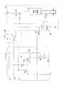
(1−1.表示装置1の全体構成)
図2は、本実施形態にかかる表示装置1の構成を示す説明図である。この図に示すように、表示装置1は、複数の画素回路Aij(iは1〜nの整数、jは1〜mの整数)と電流出力回路(ダミー画素回路)Bi(iは1〜nの整数)と、ソースドライバ回路11と、ゲートドライバ回路13と、コントロール回路12と、電流電圧変換回路14とを備えている。(1-1. Overall Configuration of Display Device 1)
FIG. 2 is an explanatory diagram illustrating a configuration of the
画素回路Aijは、複数の互いに平行に配されたデータラインSjと、これらに直交する複数の互いに平行に配された走査ラインGiとの各交差点に対応してマトリクス状に配置されている。電流出力回路Biは、走査ラインGi毎に設けられており、画素回路Aijからなる表示領域の外部に配置されており、走査ラインGiに接続された各画素回路Ai1〜Aimに備えられる駆動用TFTの特性に応じた電流を電流電圧変換回路14に帰還させるものである。電流電圧変換回路14は、電流出力回路Biから帰還した電流を電圧に変換する回路である。なお、画素回路Aij、電流出力回路Bi、および電流電圧変換回路14の詳細については後述する。 The pixel circuit Aij is arranged in a matrix corresponding to each intersection of a plurality of data lines Sj arranged in parallel to each other and a plurality of scanning lines Gi arranged orthogonal to each other. The current output circuit Bi is provided for each scanning line Gi, and is disposed outside the display area including the pixel circuit Aij. The driving TFT provided in each of the pixel circuits Ai1 to Aim connected to the scanning line Gi. The current corresponding to the characteristic is fed back to the current-
データラインSjは、ソースドライバ回路11から画素回路Aijに表示する画像データに応じたデータ信号を供給するための信号線である。また、走査ラインGiは、ゲートドライバ回路13から画素回路Aijに走査信号を供給するための信号線である。 The data line Sj is a signal line for supplying a data signal corresponding to image data to be displayed on the pixel circuit Aij from the
ソースドライバ回路11は、mビットのシフトレジスタ21と、レジスタ22と、ラッチ23と、m個のD/Aコンバータ24とを備えている。 The
シフトレジスタ21は、縦続接続されたm個のレジスタ(図示せず)を有している。このシフトレジスタ21では、コントロール回路12から先頭のレジスタに入力されるスタートパルスSPが、コントロール回路12から入力されるクロックCLKに同期して各段のレジスタを順次転送され、各段のレジスタへのスタートパルスSPの入力タイミングに応じて各段のレジスタからタイミングパルスDLPがレジスタ22へ出力される。 The shift register 21 has m registers (not shown) connected in cascade. In the shift register 21, the start pulse SP input from the
レジスタ22には、タイミングパルスDLPが入力されるタイミングでコントロール回路12から表示データDAが入力される。レジスタ22に表示データDAが一列分記憶されると、コントロール回路12からラッチ23に入力されるラッチパルスLPに同期して上記一列分の表示データDAがラッチ23に入力される。ラッチ23に保持された表示データDAのそれぞれは対応するD/Aコンバータ24へ出力される。 The display data DA is input from the
D/Aコンバータ24は、各データラインSjに対し1つずつ設けられており、ラッチ23から入力される表示データDAをアナログの信号電圧に変換して対応するデータラインSjに出力する。 One D /
ゲートドライバ回路13は、シフトレジスタ回路と、論理演算回路と、バッファとを含んでいる(いずれも図示せず)。 The
シフトレジスタ回路はn個の継続接続されたレジスタからなり、コントロール回路12からゲートドライバ回路13の先頭のレジスタに入力されたスタートパルスYIが、コントロール回路12から入力されるクロックYCKに同期して各段のレジスタ回路を順次転送され、各段のレジスタから論理演算回路に順次出力される。 The shift register circuit is composed of n continuously connected registers. The start pulse YI input from the
論理演算回路は、各段のレジスタに対応してそれぞれ設けられており、各段のレジスタ入力されたパルスとコントロール回路12から入力されたタイミング信号OEとに基づいて論理演算を行い、論理演算の結果に応じた電圧を各段の論理演算回路に対応して設けられたバッファを介して各段に対応する走査ラインGiに出力する。 The logical operation circuits are provided corresponding to the registers of the respective stages, perform logical operations based on the pulses input to the registers of the respective stages and the timing signal OE input from the
各走査ラインGiにはm個の画素回路Ai1〜Aimと電流出力回路Biとが接続されており、画素回路Ai1〜Aimはこれらのグループ単位で走査ラインGiによって走査される。これにより、各走査ラインGiに対して、ソースドライバ回路11から各データラインを介して供給されるデータ電位を当該各走査ラインGiに接続された各画素回路Ai1〜Aimに書き込むタイミングに応じた信号電圧が印加される。 Each of the scanning lines Gi is connected to m pixel circuits Ai1 to Aim and a current output circuit Bi, and the pixel circuits Ai1 to Aim are scanned by the scanning line Gi in units of these groups. Thereby, for each scanning line Gi, a signal corresponding to the timing at which the data potential supplied from the
このように、ソースドライバ回路11は、ある走査ライン1行分の画素回路へデータを一度に送信する線順次走査型の回路である。ただし、ソースドライバ回路11の構成はこれに限るものではなく、画素1つ1つに順次データを送信する点順次走査型の回路であっても構わない。点順次走査型の回路の場合、ある走査ラインの選択中は、データラインSjの電圧はデータラインの容量により保持される。なお、ここでは点順次走査型の回路についての詳細な説明は省略する。 As described above, the
コントロール回路12は、ソースドライバ回路11に、上記のスタートパルスSP、クロックCLK、表示データDA、ラッチパルスLPを出力するとともに、ゲートドライバ回路13に上記のタイミング信号OE、スタートパルスYI、クロックYCKを出力する。 The
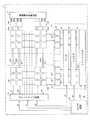
(1−2.画素回路、電流出力回路、および電流電圧変換回路の構成)
次に、表示装置1に備えられる画素回路Aij、電流出力回路Bi、および電流電圧変換回路14の構成について説明する。図1は、画素回路Aij、電流出力回路Bi、および電流電圧変換回路14の構成を示す回路図である。なお、図1は、画素回路Aij、電流出力回路Bi、および電流電圧変換回路14のうち、1本の走査ラインGiに対応する部分のみを示している。(1-2. Configuration of Pixel Circuit, Current Output Circuit, and Current-Voltage Conversion Circuit)
Next, the configuration of the pixel circuit Aij, the current output circuit Bi, and the current-
図1に示すように、画素回路Aijは、駆動用TFTであるDTFT、スイッチ用TFTであるSW、コンデンサ(保持容量)Cs、および有機EL素子ELを備えている。なお、図1では、走査ラインGiに対応する画素回路Ai1〜Aimのうち、電流出力回路Biと隣接する画素回路Aim(走査ドライバ回路13から最も離れた画素回路Aim)のみを示しているが、他の画素回路Ai1〜Aim−1についても同様の構成である。また、有機EL素子ELとしては、従来から公知の種々の有機EL素子を用いることができる。 As shown in FIG. 1, the pixel circuit Aij includes a DTFT that is a driving TFT, a SW that is a switching TFT, a capacitor (holding capacity) Cs, and an organic EL element EL. In FIG. 1, only the pixel circuit Aim (pixel circuit Aim farthest from the scan driver circuit 13) adjacent to the current output circuit Bi among the pixel circuits Ai1 to Aim corresponding to the scan line Gi is shown. The other pixel circuits Ai1 to Aim-1 have the same configuration. Moreover, conventionally well-known various organic EL elements can be used as the organic EL element EL.
電流出力回路Biは、ダミー駆動TFTであるDDTFT、スイッチ用TFTであるDSW1,DSW2,DSW3、および切替スイッチCSWを備えている。なお、本実施形態では切替スイッチCSWを電流出力回路Biに設けているが、これに限らず、電流電圧変換回路14に設けてもよく、電流出力回路Biと電流電圧変換回路14との間に独立して設けてもよい。 The current output circuit Bi includes a DDTFT serving as a dummy drive TFT, DSW1, DSW2, DSW3 serving as switching TFTs, and a changeover switch CSW. In the present embodiment, the changeover switch CSW is provided in the current output circuit Bi. However, the present invention is not limited to this, and may be provided in the current-
また、各画素回路Aijおよび各電流出力回路Biは、共通のガラス基板上に形成されており、各画素回路Aijが備えられる領域が表示領域となり、各電流出力回路Biは表示領域の外部に備えられている。また、共通の走査ライン上に備えられる画素回路と電流出力回路とについて、当該画素回路に備えられるDTFTと、当該電流出力回路に備えられるDDTFTとは、その製造工程において、レーザーアニールによる結晶化工程を同一のレーザースキャン(1回のレーザー照射)によって行われたものである。具体的には、レーザーアニールによる結晶化工程におけるレーザースキャンの主走査方向(各回のレーザースキャンにおけるレーザースポットの移動方向;長尺方法)が走査ラインGiの延伸方向と平行になっており、共通の走査ライン上に備えられる画素回路のDTFTと電流出力回路のDDTFTとは、同一のレーザースキャンによって結晶化されたものである。また、これら各DTFTとDDTFTとは形状(アスペクト比)およびサイズが同一になるように形成されている。このため、走査ラインGi上の画素回路Ai1〜Aimに備えられるDTFTと、この走査ラインGi上の電流出力回路Biに備えられるDDTFTとは、閾値(閾値電圧)や移動度といった特性(駆動能力)が実質的に同一である。 Each pixel circuit Aij and each current output circuit Bi are formed on a common glass substrate, and an area in which each pixel circuit Aij is provided becomes a display area, and each current output circuit Bi is provided outside the display area. It has been. Further, regarding the pixel circuit and the current output circuit provided on the common scanning line, the DTFT provided in the pixel circuit and the DDTFT provided in the current output circuit include a crystallization process by laser annealing in the manufacturing process. Are performed by the same laser scanning (one laser irradiation). Specifically, the main scanning direction of the laser scan in the crystallization process by laser annealing (the moving direction of the laser spot in each laser scan; the long method) is parallel to the extending direction of the scanning line Gi, The DTFT of the pixel circuit and the DDTFT of the current output circuit provided on the scan line are crystallized by the same laser scan. Each DTFT and DDFT are formed so as to have the same shape (aspect ratio) and size. For this reason, the DTFT provided in the pixel circuits Ai1 to Aim on the scan line Gi and the DDTFT provided in the current output circuit Bi on the scan line Gi have characteristics (drive capability) such as a threshold value (threshold voltage) and mobility. Are substantially the same.
電流電圧変換回路14は、カレントミラー回路CM、およびダイオード接続された電流電圧変換素子であるDrDTFTを備えている。なお、電流電圧変換回路14は、画素回路Aij毎に備えられる必要はなく、全画素回路Aijに対して少なくとも1つ備えていればよい。 The current-
なお、本実施形態では、画素回路Aij、電流出力回路Bi、および電流電圧変換回路14に備えられる各TFT(スイッチング素子)として、低温ポリシリコンTFT、CG(Continuous Grain)シリコンTFT、あるいはアモルファスシリコンTFTを用いる。これらのTFTの構成および作成プロセスは公知であるため、本実施形態ではその説明を省略する。なお、各TFTの構成はこれに限らず、他のTFTを用いてもよい。 In this embodiment, as each TFT (switching element) provided in the pixel circuit Aij, the current output circuit Bi, and the current-
また、本実施形態では、画素回路Aijに備えられるSW(スイッチ用TFT)、電流出力回路Biに備えられるDSW1,DSW2(スイッチ用TFT)、および電流電圧変換回路14に備えられるカレントミラー回路CMに備えられるTFTa,TFTbとしてNチャネル型のTFTを用いた。また、画素回路Aijに備えられるDTFT(駆動用TFT)、電流出力回路Biに備えられるDDTFT(ダミー駆動TFT)およびDSW3(スイッチ用TFT)、および電流電圧変換回路14に備えられるDrDTFT(電流電圧変換素子)としてPチャネル型のTFTを用いた。ただし、各TFTの構成はこれに限らず、本実施形態における各回路と同様の動作を実現できる構成であればよい。 In the present embodiment, the SW (switching TFT) provided in the pixel circuit Aij, the DSW1 and DSW2 (switching TFT) provided in the current output circuit Bi, and the current mirror circuit CM provided in the current-
電流電圧変換回路14に備えられるDrDTFTのソース端子は電源電位Vpを供給するラインに接続されている。また、このDrDTFTのドレイン端子は、カレントミラー回路CMを構成するTFTbのソース端子と、DrDTFT自身のゲート端子と、電流出力回路Biに備えられる切替スイッチCSWの端子cとに接続されている。 The source terminal of the DrDTFT provided in the current-
カレントミラー回路CMは、TFTaおよびTFTbの2つのTFTによって構成されている。TFTbのソース端子は上記したようにDrDTFTのドレイン端子に接続されており、TFTbのドレイン端子はGND(共通陰極)に接続されている。また、TFTbのゲート端子は、TFTaのゲート端子に接続されている。また、TFTaのドレイン端子はGNDに接続されており、TFTaのソース端子は、電流帰還ラインFB1〜DBnを介して各電流出力回路Biに備えられるDSW2のドレイン端子に接続されている。 The current mirror circuit CM is composed of two TFTs, TFTa and TFTb. The source terminal of TFTb is connected to the drain terminal of DrDTFT as described above, and the drain terminal of TFTb is connected to GND (common cathode). The gate terminal of TFTb is connected to the gate terminal of TFTa. The drain terminal of TFTa is connected to GND, and the source terminal of TFTa is connected to the drain terminal of DSW2 provided in each current output circuit Bi via current feedback lines FB1 to DBn.
電流出力回路Biに備えられる切替スイッチCSWの端子aは、容量帰還ラインCSiを介して走査ラインGiに接続された各画素回路Ai1〜AimにおけるコンデンサCsの一端に接続されている。また、切替スイッチCSWの端子bは、電流電圧変換回路14に備えられるDrDTFTのゲート端子およびドレイン端子に接続されており、切替スイッチCSWの端子cは一定電位Vrefを供給するラインに接続されている。この一定電位Vrefは表示装置1に備えられたVref生成部(図示せず)が電源電圧等に基づいて生成する。そして、切替スイッチCSWは、走査ラインGiに供給される電圧に応じて、端子a−端子b間を接続した状態と、端子a−端子c間を接続した状態とに切り替えられる。具体的には、走査ラインGiに供給される制御信号GiがL(ローレベル)の場合に端子a−端子c間が接続された状態になり、制御信号GiがH(ハイレベル)の場合に端子a−端子b間が接続された状態になる。 A terminal a of the changeover switch CSW provided in the current output circuit Bi is connected to one end of the capacitor Cs in each of the pixel circuits Ai1 to Aim connected to the scanning line Gi through the capacitive feedback line CSi. A terminal b of the changeover switch CSW is connected to a gate terminal and a drain terminal of a DrDTFT provided in the current-
電流出力回路Biに備えられるDDTFTのソース端子は、電源電位Vpを供給する端子、およびDSW3のソース端子に接続されている。また、DDTFTのドレイン端子は、DSW2のソース端子に接続されている。また、DDTFTのゲート端子は、DSW3のドレイン端子、およびDSW1のソース端子に接続されている。 A source terminal of the DDTFT provided in the current output circuit Bi is connected to a terminal for supplying the power supply potential Vp and a source terminal of the DSW3. The drain terminal of the DDTFT is connected to the source terminal of DSW2. The gate terminal of the DDTFT is connected to the drain terminal of DSW3 and the source terminal of DSW1.
DSW1〜DSW3のゲート端子は、いずれも走査ラインGiに接続されている。また、DSW1のドレイン端子は、DDTFTを駆動するダミーデータ電位Viniを供給するラインに接続されている。なお、ダミーデータ電位Viniは、画素回路Aijに対する中間調のデータ電位に相当する電位に設定することが好ましい。また、ダミーデータ電位Viniは、ソースドライバ回路11において生成されてもよく、図示しない他の回路によって生成されてもよい。 The gate terminals of DSW1 to DSW3 are all connected to the scanning line Gi. The drain terminal of DSW1 is connected to a line for supplying a dummy data potential Vini for driving the DDTFT. Note that the dummy data potential Vini is preferably set to a potential corresponding to a halftone data potential for the pixel circuit Aij. The dummy data potential Vini may be generated in the
画素回路Aijに備えられるDTFTのソース端子は、電源電位Vpを供給するライン(電流供給ラインVPi)に接続される。また、DTFTのドレイン端子は、有機EL素子ELを介してGNDに接続されている。また、DTFTのゲート端子は、コンデンサCsの他端、およびSWのドレイン端子に接続されている。なお、コンデンサCsの一端は、上記したように、電流出力回路Biに備えられる切替スイッチCSWの端子aに接続されている。 The source terminal of the DTFT provided in the pixel circuit Aij is connected to a line (current supply line VPi) that supplies the power supply potential Vp. The drain terminal of the DTFT is connected to GND via the organic EL element EL. The gate terminal of the DTFT is connected to the other end of the capacitor Cs and the drain terminal of SW. Note that one end of the capacitor Cs is connected to the terminal a of the changeover switch CSW provided in the current output circuit Bi as described above.
SWのソース端子はデータラインSjに接続されており、SWのゲート端子は走査ラインGiに接続されている。 The source terminal of SW is connected to the data line Sj, and the gate terminal of SW is connected to the scanning line Gi.
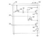
(1−3.画素回路、電流出力回路、および電流電圧変換回路の動作)
次に、表示装置1に備えられる画素回路Aij、電流出力回路Bi、および電流電圧変換回路14の動作について説明する。図3は、画素回路Aij、電流出力回路Bi、および電流電圧変換回路14の動作を示すタイミングチャートであり、この図には、走査ラインGi−1,Gi,Gi+1、容量帰還ラインCSi−1,CSi,CSi+1の信号変化のタイミングが示されている。(1-3. Operations of Pixel Circuit, Current Output Circuit, and Current-Voltage Conversion Circuit)
Next, operations of the pixel circuit Aij, the current output circuit Bi, and the current-
なお、この図に示した各走査ラインGi−1,Gi,Gi+1、および各容量帰還ラインCSi−1,CSi,CSi+1の信号は、同じデータラインSjに接続された画素回路A(i−1)j,Aij,A(i+j)jについての信号を示している。また、走査ラインGi−1および各容量帰還ラインCSi−1の信号は、走査ラインGiの前に走査される走査ラインGi−1に接続される画素回路A(i−1)jに対応しており、走査ラインGi+1および各容量帰還ラインCSi+1の信号は、走査ラインGiの次に走査される走査ラインGi+1に接続される画素回路A(i+1)jに対応している。 It should be noted that the signals of the scanning lines Gi-1, Gi, Gi + 1 and the capacitive feedback lines CSi-1, CSi, CSi + 1 shown in this figure are the pixel circuits A (i-1) connected to the same data line Sj. Signals for j, Aij, and A (i + j) j are shown. The signals of the scanning line Gi-1 and each capacitive feedback line CSi-1 correspond to the pixel circuit A (i-1) j connected to the scanning line Gi-1 scanned before the scanning line Gi. The signals of the scanning line Gi + 1 and each capacitive feedback line CSi + 1 correspond to the pixel circuit A (i + 1) j connected to the scanning line Gi + 1 scanned next to the scanning line Gi.
まず、走査ラインGiに供給する信号をHにする。これにより、画素回路AijのSWが導通し、データラインSjに供給されているデータ電位VdataがDTFTのゲート端子およびコンデンサCsの一端に供給される。また、走査ラインGiがHになったことにより、電流出力回路BiのDSW1,DSW2が導通し、DSW3が遮断される。また、切替スイッチCSWが切り替えられて容量帰還ラインCSiがDrDTFTの出力側に接続される。これにより、DDTFTのゲート端子の電位はダミーデータ電位Viniになり、電流帰還ラインFBiを介してDDTFTのコンダクタンス(DDTFTのTFT特性)に応じた電流が電流電圧変換回路14にフィードバックされる。電流電圧変換回路14にフィードバックされた電流と同じ量の電流がカレントミラー回路CMによってDrDTFTに流され、DrDTFTで電圧に変換され、容量帰還ラインCSiを介してコンデンサCsの他端の電位を変化させる。この際のコンデンサCsの他端における電位の変化量は、電流出力回路Biに備えられたDDTFTのTFT特性に依存した量になる。なお、上記変化後のコンデンサCsの他端における電位をVCSiとする。First, the signal supplied to the scanning line Gi is set to H. As a result, the SW of the pixel circuit Aij becomes conductive, and the data potential Vdata supplied to the data line Sj is supplied to the gate terminal of the DTFT and one end of the capacitor Cs. Further, when the scanning line Gi becomes H, DSW1 and DSW2 of the current output circuit Bi are turned on, and DSW3 is shut off. Further, the changeover switch CSW is switched to connect the capacitive feedback line CSi to the output side of the DrDTFT. As a result, the potential of the gate terminal of the DDTFT becomes the dummy data potential Vini, and a current corresponding to the conductance of the DDTFT (TFT characteristics of the DDTFT) is fed back to the current-
これにより、DTFTのゲート端子およびコンデンサCsの一端にデータラインSjに供給されているデータ電位Vdataに応じた電位が書き込まれるとともに、DDTFTのTFT特性が検出されてこのTFT特性に応じた電位がコンデンサCsの他端に書き込まれる。 As a result, the potential corresponding to the data potential Vdata supplied to the data line Sj is written to the gate terminal of the DTFT and one end of the capacitor Cs, and the TFT characteristics of the DDTFT are detected and the potential corresponding to the TFT characteristics is Written at the other end of Cs.
その後、走査ラインGiの選択期間が終了し、走査ラインGiがLになると、電流出力回路Biから電流電圧変換回路14への電流帰還ラインFBiを介した電流の帰還が遮断されるとともに、切替スイッチCSWが切り替えられて容量帰還ラインCSiが一定電位Vrefを供給するラインに接続される。その結果、DTFTのゲート電位はVCSi−Vrefだけシフト(変化)する。これにより、DTFTのTFT特性のばらつきが補償される。Thereafter, when the selection period of the scanning line Gi ends and the scanning line Gi becomes L, the feedback of the current through the current feedback line FBi from the current output circuit Bi to the current-
上記の動作によってDTFTのTFT特性のばらつきが補償される理由について以下に説明する。 The reason why variation in TFT characteristics of the DTFT is compensated by the above operation will be described below.
一般に、TFTの飽和領域においては、ドレーン−ソース間を流れる電流IELは、ゲート−ソース間電圧をVgsとしたとき、チャネル長変調効果を無視すれば、
IEL=1/2・W/L・Cox・μ(Vgs−Vth)2・・・(1)
で表される。ここで、W/LはTFTのアスペクト比、CoxはTFTのゲート容量、μはTFTの移動度、VthはTFTの閾値(閾値電圧)である。したがって、DTFTのドレーン−ソース間を流れる電流IELは、DTFTの閾値に依存したものとなる。Generally, in the saturation region of a TFT, the current IEL flowing between the drain and the source can be ignored if the channel length modulation effect is ignored when the gate-source voltage is Vgs.
IEL = 1/2 · W / L · Cox · μ (Vgs−Vth)2 (1)
It is represented by Here, W / L is the TFT aspect ratio, Cox is the TFT gate capacitance, μ is the TFT mobility, and Vth is the TFT threshold (threshold voltage). Therefore, the current IEL flowing between the drain and the source of the DTFT depends on the threshold value of the DTFT.
ここで、あらかじめゲート−ソース間に与える信号電圧Vgsを、データ電位VdataにVthだけオフセットを加えた電圧、すなわち、Vgs=Vdata+Vthとしておけば、
IEL=1/2・W/L・Cox・μ(Vdata)2 ・・・(2)
となり、ドレーン−ソース間を流れる電流IELは、閾値Vthのばらつきの影響を受けることがなくなる。なお、上記(1)式は、DDTFTについてもそのまま適用できる。また、上述したように、DTFTとDDTFTの閾値Vthは、略同一の値である。Here, if the signal voltage Vgs given between the gate and the source is previously set to a voltage obtained by adding an offset by Vth to the data potential Vdata, that is, Vgs = Vdata + Vth,
IEL = 1/2 · W / L · Cox · μ (Vdata)2 (2)
Thus, the current IEL flowing between the drain and the source is not affected by the variation in the threshold value Vth. The above equation (1) can be applied to the DDTFT as it is. Further, as described above, the threshold values Vth of the DTFT and the DDTFT are substantially the same value.
上記したように、走査ラインGiがHになったとき、DDTFTを流れる電流は電流帰還ラインFBiを介して電流電圧変換回路14に帰還し、帰還した電流と同じ量の電流がカレントミラー回路CMによってDrDTFTに流れる。この時、ダイオード接続されたDrDTFTの両端の電圧VgsDrは、 As described above, when the scanning line Gi becomes H, the current flowing through the DDTFT is fed back to the current-

となる。ここで、IELはDrTFTのドレーン−ソース間を流れる電流、μnはDrTFTの移動度、CoxはDrTFTのゲート容量、WD/LDはDrTFTのアスペクト比、VthDrはDrDTFTの閾値である。It becomes. Here, IEL is the current flowing between the drain and source of the DrTFT, μn is the mobility of the DrTFT, Cox is the gate capacitance of the DrTFT, WD / LD is the aspect ratio of the DrTFT, and VthDr is the threshold of the DrDTFT.
ここで、DrTFTとDDTFTのアスペクト比が同一ならば、
VgsDr=VgsD−VthD+VthDr
が成り立つ。したがって、選択期間中、容量帰還ラインCSiの電位VCSiは、
VCSi=Vp−VgsDr
=Vp−VgsD+VthD−VthDr
となる。ここで、選択期間中(走査ラインGiがHの期間中)は、DDTFTのゲート電位はダミーデータ電位Viniなので、
Vini=Vp−VgsDである。したがって、
VCSi=Vini+VthD−VthDr
となっている。Here, if the aspect ratio of DrTFT and DDTFT is the same,
VgsDr = VgsD−VthD + VthDr
Holds. Therefore, during the selection period, the potential VCSi of the capacitive feedback lineCSi is
VCSi = Vp-VgsDr
= Vp-VgsD + VthD-VthDr
It becomes. Here, during the selection period (during the scanning line Gi is H), the gate potential of the DDTFT is the dummy data potential Vini.
Vini = Vp−VgsD. Therefore,
VCSi = Vini + VthD−VthDr
It has become.
また、選択期間中、DTFTのゲート端子にはデータラインSjに供給されたデータ電位Vdataが書き込まれている。 Further, during the selection period, the data potential Vdata supplied to the data line Sj is written to the gate terminal of the DTFT.
その後、選択期間が終了し(走査ラインGiがLになり)、容量帰還ラインCSiの電位が一定電位Vrefに変化すると、DTFTのゲート電位Vgは、理想的には、
Vg=Vdata+Vini+VthD−VthDr−Vref
IEL=k・(Vdata+Vini+VthD−VthDr−Vref−Vth)2・・・(3)
となる。ここで、DTFTの閾値VthとDDTFTの閾値VthDは等しいので、
IEL=k・(Vdata+Vini−VthDr−Vref)2
である。Thereafter, when the selection period ends (the scanning line Gi becomes L) and the potential of the capacitive feedback line CSi changes to the constant potential Vref, the gate potential Vg of the DTFT is ideally
Vg = Vdata + Vini + VthD−VthDr−Vref
IEL = k · (Vdata + Vini + VthD−VthDr−Vref−Vth)2 (3)
It becomes. Here, since the threshold Vth of the DTFT and the threshold VthD of the DDTFT are equal,
IEL = k · (Vdata + Vini−VthDr−Vref)2
It is.
したがって、各画素回路Aijに備えられたDTFTの閾値Vth(TFT特性)のばらつきを補償できる。つまり、表示画面の各行(各走査ライン)について、これら各行間におけるDTFTのTFT特性のばらつきを補償し、DTFTのTFT特性のばらつきに起因して筋状の画像欠陥が生じることを防止できる。 Therefore, it is possible to compensate for variations in the threshold value Vth (TFT characteristics) of the DTFT provided in each pixel circuit Aij. That is, for each row (each scanning line) on the display screen, variations in the TFT characteristics of the DTFT between these rows can be compensated, and streak image defects can be prevented from occurring due to variations in the TFT characteristics of the DTFT.
以上のように、本実施形態にかかる表示装置1は、走査ラインGi毎に、この走査ラインGiに接続された画素回路Aijに備えられるDTFTと実質的に同じTFT特性を有するDDTFT(ダミー駆動TFT)を備えている。そして、DDTFTのゲート端子にダミーデータ電位Viniを供給したときにDDTFTを流れる電流を電流電圧変換回路14に帰還させ、この電流を電圧に変換した結果に基づいて各画素回路AijのDTFTのゲート電位を制御する。 As described above, in the
これにより、走査ラインGi毎のDTFTのTFT特性のばらつきを補償することができるので、DTFTのTFT特性のばらつきに起因する筋状の画像欠陥を防止できる。 As a result, variations in the TFT characteristics of the DTFT for each scanning line Gi can be compensated, so that streak-like image defects due to variations in the TFT characteristics of the DTFT can be prevented.
また、従来の補正型画素回路(画素回路にばらつき補償機能を設けた従来の構成)に比べて、画素回路の構成を簡略化して回路規模を小さくできる。また、電流出力回路Bi、および電流電圧変換回路14を表示領域の外部に配置することができるので、従来の補正型画素回路を備えた表示装置よりも画素の開口率を向上させることができる。 In addition, the configuration of the pixel circuit can be simplified and the circuit scale can be reduced as compared with a conventional correction pixel circuit (conventional configuration in which a variation compensation function is provided in the pixel circuit). In addition, since the current output circuit Bi and the current-
また、電流電圧変換回路14は、カレントミラー回路CMと電流電圧変換素子DrDTFTとによって構成される簡便な構成で実現できる。また、電流電圧変換回路14は、全画素回路Aijに対して1つだけ備えればよい。このため、外部回路の回路規模の増大を最小限に抑えることができる。ただし、電流電圧変換回路14の数はこれに限るものではない。 The current-
また、本実施形態では、電流出力回路Biを走査ラインGi毎に1つずつ設けるだけでいいので、外部回路の回路規模の増大を抑制できる。なお、本実施形態は、電流出力回路Biを走査ラインGi毎に設けているが、これに限らず、例えば複数の走査ライン毎に設けてもよい。ただし、切替スイッチCSWについては走査ライン毎に設けることが好ましい。 Further, in the present embodiment, it is only necessary to provide one current output circuit Bi for each scanning line Gi, so that an increase in the circuit scale of the external circuit can be suppressed. In the present embodiment, the current output circuit Bi is provided for each scanning line Gi. However, the present invention is not limited to this. For example, the current output circuit Bi may be provided for each of a plurality of scanning lines. However, the changeover switch CSW is preferably provided for each scanning line.
また、本実施形態では、共通の走査ラインに接続されている各画素回路Aijおよび電流出力回路Biについて、当該各画素回路AijのDTFTと当該電流出力回路BiのDDTFTとは、レーザーアニールによる結晶化工程を同一のレーザースキャンによって行われたものであり、その形状およびサイズが同じである。このため、共通の走査ラインGiに対応するDTFTとDDTFTとは、閾値や移動度といった駆動能力が実質的に同一である。したがって、DDTFTを流れる電流に基づいてこのDDTFTが備えられる電流出力回路Biと同じ走査ラインGiに接続される画素回路AijのDTFTのゲート電位を制御することにより、副走査方向(データラインSjの延伸方向)についてのDTFTの閾値特性のばらつきを精度よく補償することができる。また、レーザーの継ぎ目でのDTFTの閾値特性のばらつきを精度よく補償することができる。 In this embodiment, for each pixel circuit Aij and current output circuit Bi connected to a common scanning line, the DTFT of each pixel circuit Aij and the DDFT of the current output circuit Bi are crystallized by laser annealing. The process is performed by the same laser scanning, and the shape and size are the same. For this reason, the DTFT and DDTFT corresponding to the common scanning line Gi have substantially the same driving capability such as threshold value and mobility. Therefore, by controlling the gate potential of the DTFT of the pixel circuit Aij connected to the same scanning line Gi as the current output circuit Bi provided with the DDFT based on the current flowing through the DDFT, the sub-scanning direction (the extension of the data line Sj) is controlled. Variation in threshold characteristics of the DTFT with respect to (direction) can be compensated with high accuracy. In addition, it is possible to accurately compensate for variations in threshold characteristics of the DTFT at the laser joint.
なお、レーザーアニールの幅(同一のレーザースキャンにおける副走査方向の幅)が各画素回路Aijの副走査方向の幅よりも大きい場合、このレーザーアニールの幅に含まれる走査ライン毎に、電流出力回路を1つずつ設けるようにしてもよい。この場合、1回のレーザースキャンのスキャン範囲に含まれる各走査ラインに対応する各画素回路のDTFTのTFT特性と、このスキャン範囲に含まれる電流出力回路のDDTFTのTFT特性とは実質的に同じになる。したがって、副走査方向(データラインSjの延伸方向)についてのDTFTの閾値特性のばらつき、特にレーザーの継ぎ目でのDTFTの閾値特性のばらつきを精度よく補償することができる。また、電流出力回路の数を削減し、回路規模を低減することができる。 When the width of laser annealing (width in the sub-scanning direction in the same laser scan) is larger than the width of each pixel circuit Aij in the sub-scanning direction, a current output circuit is provided for each scanning line included in the laser annealing width. May be provided one by one. In this case, the TFT characteristics of the DTFT of each pixel circuit corresponding to each scanning line included in the scanning range of one laser scan and the TFT characteristics of the DTFT of the current output circuit included in this scanning range are substantially the same. become. Therefore, variations in the threshold characteristics of the DTFT in the sub-scanning direction (the extending direction of the data line Sj), in particular, variations in the threshold characteristics of the DTFT at the laser joint can be accurately compensated. Further, the number of current output circuits can be reduced and the circuit scale can be reduced.
また、本実施形態では、上述したように、走査ラインGiの選択期間後にこの走査ラインGiに接続された各画素回路Ai1〜Aimに備えられるDTFTのゲート電位をこれら各DTFTの駆動能力(閾値)に応じて変化させる。ところが、このゲート電位の変化量は、コンデンサCsとDTFTの寄生容量Cgs(図1参照)とによって減衰してしまう場合がある。 In the present embodiment, as described above, the gate potential of the DTFT provided in each of the pixel circuits Ai1 to Aim connected to the scanning line Gi after the selection period of the scanning line Gi is used as the drive capability (threshold value) of each DTFT. It changes according to. However, the amount of change in the gate potential may be attenuated by the capacitor Cs and the parasitic capacitance Cgs of the DTFT (see FIG. 1).
そこで、このゲート電位の変化量の減衰を補うために、図4に示すように、電流電圧変換回路14に備えられるDrDTFTの出力側(DrDTFTのゲート端子)に、アンプ(バッファアンプ)OAを設け、このアンプOAのゲインAvを1以上に設定してもよい。なお、このアンプOAのゲインAvは、コンデンサCsの容量をCs、DTFTの寄生容量をCgsとすると、Av=Cs+Cgs/Cs程度に設定することが好ましい。これにより、カップリングによる上記変化量の減衰を補償することができる。また、DrDTFTからの出力信号を、アンプOAを介して出力することにより、容量帰還ラインCSiを低出力インピダンスにしてその駆動能力を上昇させることができる。 Therefore, in order to compensate for the attenuation of the change amount of the gate potential, an amplifier (buffer amplifier) OA is provided on the output side of the DrDTFT (gate terminal of DrDTFT) provided in the current-
〔実施形態2〕
本発明の他の実施形態について説明する。なお、説明の便宜上、実施形態1と同じ機能を有する部材については同じ符号を付し、その説明を省略する。[Embodiment 2]
Another embodiment of the present invention will be described. For convenience of explanation, members having the same functions as those in the first embodiment are denoted by the same reference numerals, and description thereof is omitted.
実施形態1では、各画素回路Aijによって構成される表示領域(有効表示エリア)に隣接する位置に電流出力回路(ダミー画素)Biを設け、この電流出力回路Biから電流電圧変換回路14への帰還電流に基づいて各画素回路Aijに備えられるDTFT(駆動TFT)のゲート電位を制御していた。これに対して、本実施形態では、電流出力回路Biを設けず、画素回路Aijから電流電圧変換回路14に電流を帰還させ、この帰還電流に基づいて各画素回路Aijに備えられるDTFTのゲート電位を制御する。 In the first embodiment, a current output circuit (dummy pixel) Bi is provided at a position adjacent to a display area (effective display area) constituted by each pixel circuit Aij, and feedback from the current output circuit Bi to the current-
図5は、本実施形態にかかる表示装置1bの概略構成を示す説明図である。この図に示すように、表示装置1bは、電流出力回路(ダミー画素)Biが設けられていない点、電流電圧変換回路14への電流帰還ラインFBiが共通の走査ラインGiに対応する各画素回路Ai1〜Aimと電流電圧変換回路14とを結ぶように設けられている点、およびゲートドライバ回路13から共通の走査ラインGiに対応する各画素回路Ai1〜Aimに切替信号Eiを供給するための切替信号ラインEiが設けられている点が異なっている。上記の切替信号の詳細については後述する。 FIG. 5 is an explanatory diagram showing a schematic configuration of the
図6は、表示装置1bに備えられる画素回路Aijおよび電流電圧変換回路14の構成を示す回路図である。 FIG. 6 is a circuit diagram showing the configuration of the pixel circuit Aij and the current-
この図に示すように、各画素回路Aijは、実施形態1の表示装置1における各画素回路Aijの構成に加えて、スイッチ用TFTであるSW2,SW3を備えている。本実施形態では、SW2としてNチャネル型のTFT、SW3としてPチャネル型のTFTを用いた。 As shown in this figure, each pixel circuit Aij includes SW2 and SW3, which are switching TFTs, in addition to the configuration of each pixel circuit Aij in the
SW2のソース端子はDTFTのドレイン端子に接続されており、ドレイン端子は電流帰還ラインFBiに接続されており、ゲート端子は切替信号ラインEiに接続されている。SW3のソース端子はDTFTのドレイン端子に接続されており、ドレイン端子は有機EL素子ELに接続されており、ゲート端子は切替信号ラインEiに接続されている。 The source terminal of SW2 is connected to the drain terminal of the DTFT, the drain terminal is connected to the current feedback line FBi, and the gate terminal is connected to the switching signal line Ei. The source terminal of SW3 is connected to the drain terminal of the DTFT, the drain terminal is connected to the organic EL element EL, and the gate terminal is connected to the switching signal line Ei.
切替信号ラインEiは、ゲートドライバ回路13に接続されており、ゲートドライバ回路13から走査ラインGiに接続された各画素回路Aijへ、走査ラインGiの選択期間を前半期間と後半期間とに分割するための切替信号Eiを供給する。上記の切替信号Eiは、Gi同様、ゲートドライバ回路13がコントロール回路12から入力される信号に基づいて生成する。具体的には、例えば、周期がクロックYCKと同一であるゲーテドクロックECKをコントロール回路12からゲートドライバ13に入力し、制御信号GiとゲーテドクロックECKとの論理積により切替信号Eiを生成する方法が考えられる。この場合、切替信号Eiの幅(周期)はゲーテドクロックECKの幅(周期)に等しくなる。前半期間および後半期間の長さは同じでなくてもよい。 The switching signal line Ei is connected to the
電流電圧変換回路14は、実施形態1の表示装置1における電流電圧変換回路14の構成に加えて、電流ラッチ回路31を備えている。電流ラッチ回路31の詳細については後述する。なお、本実施形態では、実施形態1と異なり、走査ラインGiに接続された各画素回路Aijからの帰還電流が電流電圧変換回路14に帰還することになるので、カレントミラー回路CMの面積比やDrDTFTのサイズを適宜調整すればよい。例えば、1走査行あたりm個の電流出力回路が設けられている場合、DrDTFTとDTFTのアスペクト比を同一にし、カレントミラーの面積比をTFTa:TFTb=m:1とするように調整してもよい。 The current-
図7は、表示装置1bにおける画素回路Aij、および電流電圧変換回路14の動作を示すタイミングチャートである。 FIG. 7 is a timing chart showing operations of the pixel circuit Aij and the current-
まず、走査ラインGiに供給する信号および切替信号ラインEiに供給する切替信号EiをHにする。これにより、画素回路AijのSWが導通し、データラインSjに供給されているデータ電位VdataがDTFTのゲート端子およびコンデンサCsの一端に供給される。また、SW2が導通し、SW3が遮断される。これにより、電流帰還ラインFBiを介してDTFTのコンダクタンス(DTFTのTFT特性)に応じた電流が電流電圧変換回路14にフィードバックされる。これにより、電流電圧変換回路14にフィードバックされた電流と同じ量の電流が電流電圧変換回路14のカレントミラー回路CMによって電流ラッチ回路31でラッチされるとともに、DrDTFTに流れる。これにより、DrDTFTで電流が電圧に変換され、実施形態1と同様に、容量帰還ラインCSiを介してコンデンサCsの他端の電位がVCSiに変化する。このときのコンデンサCsの他端における電位の変化量は、画素回路Ai1〜Aimに備えられた各DTFTの閾値(TFT特性)の平均値に依存した量になる。なお、選択期間の前半期間には、データラインSjにはダミーデータ電位Viniが供給される。ダミーデータ電位Viniは、画素回路Aijに対する中間調のデータ電位に相当する電位に設定することが好ましい。First, the signal supplied to the scanning line Gi and the switching signal Ei supplied to the switching signal line Ei are set to H. As a result, the SW of the pixel circuit Aij becomes conductive, and the data potential Vdata supplied to the data line Sj is supplied to the gate terminal of the DTFT and one end of the capacitor Cs. Further, SW2 is conducted and SW3 is shut off. As a result, a current corresponding to the conductance of the DTFT (DTFT TFT characteristics) is fed back to the current-
その後、切替信号EiをLにして選択期間の後半期間に切り替える。切替信号EiがLになると、SW2が遮断され、SW3が導通する。また、電流電圧変換回路14に備えられた電流ラッチ回路31の動作が切り替えられ、電流ラッチ回路31にラッチされていた電流がDrDTFTに流れる。そして、この電流がDrDTFTで電圧に変換される。なお、選択期間の前半期間に電流帰還ラインFBiを介して電流電圧変換回路14に帰還した電流は電流ラッチ回路31でラッチされているので、容量帰還ラインCSiの電位は選択期間の前半期間と後半期間とで変わらない。選択期間の後半期間には、データラインSjには画像データに応じたデータ電位Vdataが供給される。 Thereafter, the switching signal Ei is set to L to switch to the second half of the selection period. When the switching signal Ei becomes L, SW2 is cut off and SW3 is turned on. Further, the operation of the
これにより、DTFTのゲート端子およびコンデンサCsの一端にデータラインSjに供給されているデータ電位Vdataに応じた電位が書き込まれるとともに、DTFTのTFT特性が検出されてこの閾値に応じた電位がコンデンサCsの他端に書き込まれる。 As a result, a potential corresponding to the data potential Vdata supplied to the data line Sj is written to the gate terminal of the DTFT and one end of the capacitor Cs, and the TFT characteristics of the DTFT are detected and the potential corresponding to the threshold is set to the capacitor Cs. Is written at the other end.
その後、走査ラインGiの選択期間が終了し、走査ラインGiがLになると、各画素回路Ai1〜Aimから電流電圧変換回路14への電流帰還ラインFBiを介した電流の帰還が遮断されるとともに、切替スイッチCSWが切り替えられて容量帰還ラインCSiが一定電位Vrefを供給するラインに接続される。その結果、DTFTのゲート電位は、実施形態1と同様、VCSi−Vrefだけシフトする。これにより、DTFTのTFT特性のばらつきが補償される。Thereafter, when the selection period of the scanning line Gi ends and the scanning line Gi becomes L, current feedback via the current feedback line FBi from the pixel circuits Ai1 to Aim to the current-
以上のように、本実施形態にかかる表示装置1では、同一の走査ラインGiに接続されている各画素回路Ai1〜Aimから電流電圧変換回路14にDTFTのコンダクタンスに応じた電流を帰還させ、この帰還電流に基づいて各DTFTのゲート電位を制御する。これにより、同一の走査ラインGiに接続されている全画素回路に備えられるDTFTのコンダクタンスに応じた電流の平均値に基づいて各DTFTの駆動電圧を制御できる。したがって、各画素回路に備えられるDTFTのTFT特性のばらつきに起因する表示品位の低下をより高精度に補償することができる。 As described above, in the
なお、図4に示した例と同様、電流電圧変換回路14に備えられるDrDTFTの出力側(DrDTFTのゲート端子)に、アンプOAを設け、ゲインAvが1以上のアンプOAの設定してもよい。 As in the example shown in FIG. 4, an amplifier OA may be provided on the output side of the DrDTFT provided in the current-voltage conversion circuit 14 (the gate terminal of the DrDTFT), and the amplifier OA having a gain Av of 1 or more may be set. .
また、本実施形態では、同一の走査ラインGiに接続された各画素回路Ai1〜Aimを全て電流帰還ラインFBiに接続することにより、これら各画素回路Ai1〜Aimに備えられるDTFTのコンダクタンスに応じた電流の平均値に基づいてこれら各DTFTのTFT特性のばらつきを補償しているが、これに限るものではない。 Further, in the present embodiment, all the pixel circuits Ai1 to Aim connected to the same scanning line Gi are connected to the current feedback line FBi, so that the conductance of the DTFT provided in each of the pixel circuits Ai1 to Aim is determined. Although variations in TFT characteristics of each DTFT are compensated based on the average value of the current, the present invention is not limited to this.
実施形態1で説明したように、共通の走査ラインGiに接続されている各画素回路Aijは、当該各画素回路AijのDTFTの製造工程において、レーザーアニールによる結晶化工程を同一のレーザースキャンによって行い、その形状およびサイズが同じになるように形成されている。この場合、共通の走査ラインGiに対応する各DTFTは、TFT特性が実質的に同一でなる。 As described in the first embodiment, each pixel circuit Aij connected to the common scanning line Gi performs a crystallization process by laser annealing by the same laser scan in the manufacturing process of the DTFT of each pixel circuit Aij. The shape and size are the same. In this case, the TFT characteristics of the DTFTs corresponding to the common scanning line Gi are substantially the same.
そこで、例えば、同一の走査ラインGiに接続された各画素回路Aijのうちの1つ以上の画素回路を電流帰還ラインBFiに接続し、当該画素回路に備えられるDTFTのコンダクタンスに応じた電流に基づいて画素回路Aijに備えられるDTFTのTFT特性のばらつきを補償するようにしてもよい。 Therefore, for example, one or more pixel circuits among the pixel circuits Aij connected to the same scanning line Gi are connected to the current feedback line BFi, and based on the current according to the conductance of the DTFT provided in the pixel circuit. Thus, variations in TFT characteristics of the DTFT provided in the pixel circuit Aij may be compensated.
これにより、画素回路に備えられるDTFTのTFT特性のばらつき(レーザースキャンの副走査方向(データラインSjの延伸方向)についてのDTFTのTFT特性のばらつき)に起因する筋状の画像欠陥を精度よく防止するとともに、電流帰還ラインFBiに接続されていない画素回路の回路構成を簡略化することができる。また、表示領域内に設けられる電流帰還ラインFBiの長さ(占有面積)を短くすることができる。 As a result, it is possible to accurately prevent streak-like image defects caused by variations in TFT characteristics of the DTFT provided in the pixel circuit (variations in TFT characteristics of the DTFT in the sub-scanning direction of the laser scan (the extending direction of the data line Sj)). In addition, the circuit configuration of the pixel circuit that is not connected to the current feedback line FBi can be simplified. In addition, the length (occupied area) of the current feedback line FBi provided in the display region can be shortened.
〔実施形態3〕
本発明のさらに他の実施形態について説明する。なお、説明の便宜上、上述の実施形態と同様の機能を有する部材には同じ符号を付し、その説明を省略する。[Embodiment 3]
Still another embodiment of the present invention will be described. For convenience of explanation, members having the same functions as those of the above-described embodiment are denoted by the same reference numerals, and description thereof is omitted.
実施形態1,2では、同一の走査ラインに接続されている各画素回路に備えられる各DTFTの電流能力(各DTFTのコンダクタンスに応じた電流)を検出し、この電流能力に応じてDTFTのゲート電位を制御することで走査ライン毎のDTFTの閾値のばらつきを補償していた。ただし、実施形態1,2では、同一の走査ラインに接続されている画素回路毎のDTFTのTFT特性のばらつきについては補償していなかった。これに対して、本実施形態では、走査ライン毎のDTFTの閾値のばらつきに加えて、同一の走査ラインに接続されている画素回路毎のDTFTのTFT特性のばらつきをも補償する。 In the first and second embodiments, the current capability of each DTFT provided in each pixel circuit connected to the same scan line (current corresponding to the conductance of each DTFT) is detected, and the gate of the DTFT is detected according to this current capability. By controlling the potential, variations in the threshold value of the DTFT for each scanning line were compensated. However, in the first and second embodiments, variations in TFT characteristics of the DTFT for each pixel circuit connected to the same scanning line are not compensated. On the other hand, in this embodiment, in addition to variations in the threshold value of the DTFT for each scanning line, variations in TFT characteristics of the DTFT for each pixel circuit connected to the same scanning line are also compensated.
図8は、本実施形態にかかる表示装置1cの概略構成を示す説明図である。なお、本実施形態では、実施形態1にかかる表示装置1に同一の走査ラインに接続されている画素回路毎のDTFTにおけるTFT特性のばらつきを補償するための構成を付加した実施例について説明するが、実施形態2にかかる表示装置1bに同様の構成を付加してもよい。 FIG. 8 is an explanatory diagram illustrating a schematic configuration of the display device 1c according to the present embodiment. In the present embodiment, an example will be described in which the
図8に示すように、表示装置1cは、実施形態1における表示装置1の構成に加えて、電流測定素子Mj、メモリ素子42、および演算素子43を備えている。 As illustrated in FIG. 8, the display device 1 c includes a current measurement element Mj, a
電流測定素子Mjは、電源41から各画素回路Aijの有機EL素子ELに電流を供給するための電流供給ラインVpi毎に備えられ、これら各電流供給ラインVpiに流れる電流を測定する。なお、各電流供給ラインM1〜Mmは、それぞれ、データラインS1〜Smに接続された画素回路に電流を供給するようになっている。 The current measuring element Mj is provided for each current supply line Vpi for supplying current from the
メモリ素子42は、各電流測定素子Mjによる電流測定結果を記憶するためのものであり、このメモリ素子42は、演算素子43を介してソースドライバ回路11に接続されている。 The
演算素子43は、コントロール回路12とソースドライバ回路11のレジスタ22との間に備えられている。そして、この演算素子43は、コントロール回路12から出力された各データラインSjに対応する表示データDAをメモリ素子42に記憶されている各電流供給ラインMjについての電流測定結果に基づいて各画素回路に備えられるDTFTのTFT特性のばらつきを補償するように補正してソースドライバ回路11のレジスタ22に出力する。 The
次に、電流測定素子Mjによる電流測定方法、およびメモリ素子42に記憶させる電流測定結果について説明する。 Next, a current measurement method using the current measurement element Mj and a current measurement result stored in the
まず、走査ラインG1に走査電圧(Hの電圧)を与えて、走査ラインG1上の各画素回路A11〜Am1に備えられているSWを導通させる。なお、この際の電流出力回路Biおよび電流電圧変換回路14の動作は実施形態1で説明した動作と同様である。また、これと同期して、各データラインSjを介して所定のデータ電位(例えば、電流−輝度特性において輝度を等分割した場合に相当する電流を実現するための電圧)を入力する。実施形態1と同様の補償が行われた後、各画素回路A11〜Am1におけるDTFTには、コンデンサCsに蓄積された電荷量に応じて、電流供給ラインVPjから各画素回路A11〜Am1に備えられた有機EL素子ELに電流が流れ込む。このときのDTFTのゲート電位は、データ電位を選択行のDTFTの電流能力(たとえば平均値)により補償した電位になっており、それに応じた電流が有機EL素子ELに流れる。この際、各有機EL素子ELに流れる電流量を電流測定素子Mjによって測定する。なお、上記の測定結果をメモリ素子42あるいはメモリ素子42とは異なる他の記憶素子(図示せず)に一端記憶させておくようにしてもよい。また、電流測定素子Mjの構成は特に限定されるものではなく、電流量を測定できるものであればよい。 First, a scanning voltage (H voltage) is applied to the scanning line G1, and the SWs provided in the pixel circuits A11 to Am1 on the scanning line G1 are turned on. The operations of the current output circuit Bi and the current-
その後、再び走査ラインG1に走査電圧を与えて、走査ラインG1上の各画素回路A11〜Am1に備えられているSWを導通させる。なお、この際の電流出力回路Biおよび電流電圧変換回路14の動作は実施形態1で説明した動作と同様である。また、これと同期して、各データラインSjを介して有機EL素子ELを0階調にするためのデータ電位を入力する。これにより、走査ラインG1上の各画素回路A11〜Am1に備えられた有機EL素子ELに電流が流れなくなる。 Thereafter, a scanning voltage is again applied to the scanning line G1, and the SWs provided in the pixel circuits A11 to Am1 on the scanning line G1 are turned on. The operations of the current output circuit Bi and the current-
走査ラインG1に対して行った上記の走査を、走査ラインG2〜Gnについても順次行っていく。これにより、各有機EL素子ELに流れる電流値を全て測定する。そして、各電流供給ラインVPjに接続されている各画素回路の有機EL素子ELに流れる電流量の平均値あるいは総和を電流供給ラインVpi毎に算出して算出結果をメモリ素子42に記憶させる。 The above scanning performed on the scanning line G1 is sequentially performed on the scanning lines G2 to Gn. As a result, all current values flowing through the organic EL elements EL are measured. Then, an average value or a sum of current amounts flowing through the organic EL elements EL of the pixel circuits connected to the current supply lines VPj is calculated for each current supply line Vpi, and the calculation result is stored in the
なお、上記電流量の測定処理、上記平均値あるいは上記総和の算出処理、および算出結果の記憶処理は、例えば、表示装置1cの製造時、ユーザーからの指示があったとき、メンテナンス時、これらの処理を前回行ったときからの経過時間あるいは表示装置1cの累積使用時間が所定時間に達した時などに行うようにすればよい。 The current amount measurement process, the average value or the total sum calculation process, and the calculation result storage process are performed, for example, when the display device 1c is manufactured, when an instruction is given from the user, or during maintenance. What is necessary is just to perform it, for example, when the elapsed time from the previous processing or when the accumulated usage time of the display device 1c has reached a predetermined time.
表示装置1cにおいて画像表示を行うときには、まず、コントロール回路12から出力された各データラインSjに対応する表示データDAを、演算素子43が、メモリ素子42に記憶させておいた電流供給ラインVPj毎の電流量の平均値あるいは総和に基づいて、走査ラインGiの延伸方向に並ぶ各画素回路AijのDTFTのTFT特性のばらつきを補償するように補正し、ソースドライバ回路11に出力する。その後、実施形態1で説明した動作と同様の動作を行って画像表示を行う。 When an image is displayed on the display device 1c, first, the display data DA corresponding to each data line Sj output from the
以上のように、本実施形態にかかる表示装置1cは、所定のデータ電位を供給したときに有機EL素子ELに流れる電流量を各画素回路について測定し、同一の電流供給ラインVPjに接続されている各画素回路についての上記電流量の平均値あるいは総和をメモリ素子42に記憶させておく。そして、画像表示を行う際、演算素子43が、コントロール回路12から出力される各データラインSjに対応する表示データDAを、メモリ素子42に記憶させておいた上記電流量の平均値あるいは総和に基づいて補正する。その後、実施形態1と同様の駆動を行って画像表示を行う。 As described above, the display device 1c according to the present embodiment measures the amount of current flowing through the organic EL element EL when a predetermined data potential is supplied for each pixel circuit, and is connected to the same current supply line VPj. The average value or sum of the current amounts for each pixel circuit is stored in the
これにより、実施形態1にかかる表示装置1と同様、走査ラインGi毎のDTFTのTFT特性のばらつきに起因する筋状の画像結果を防止できる。さらに、走査ラインGiの延伸方向に並ぶ各画素回路におけるDTFTのTFT特性のばらつきに起因する画像欠陥(画像の表示むら)についても抑制することができる。したがって、DTFTのTFT特性のばらつきに起因する画像欠陥をより高精度に補償できる。 As a result, similar to the
また、表示装置1cでは、実施形態1にかかる表示装置1と同様の補償を行った上での電流値をメモリ素子に記憶させる。したがって、上記特許文献2と比較して、1画素あたりの電流のばらつきは行単位の補償をした分小さくなる。このため、1画素あたりの電流値を記憶するメモリのビット数の削減が可能であり、結果としてメモリ素子42の記憶容量を低減できる。 Further, in the display device 1c, the current value after performing the same compensation as in the
本発明は上述した実施形態に限定されるものではなく、請求項に示した範囲で種々の変更が可能である。すなわち、請求項に示した範囲で適宜変更した技術的手段を組み合わせて得られる実施形態についても本発明の技術的範囲に含まれる。 The present invention is not limited to the above-described embodiments, and various modifications can be made within the scope shown in the claims. That is, embodiments obtained by combining technical means appropriately modified within the scope of the claims are also included in the technical scope of the present invention.
本発明は、電流制御型の表示装置に適用できる。 The present invention can be applied to a current control type display device.
Claims (12)
Translated fromJapanese上記各画素回路は、一端側を上記駆動用TFTのゲート端子に接続され、他端側を容量帰還ラインに接続された保持容量を有しており、
選択期間中の画素回路における上記駆動用TFTのゲート端子に所定電位を供給したときにこの駆動用TFTに流れる電流である帰還電流を入力端子に入力され、入力された帰還電流を電圧に変換し、変換した電圧に応じた電位を出力端子から出力する電流電圧変換回路と、
選択期間中の上記画素回路に対応する上記容量帰還ラインを上記電流電圧変換回路の出力端子に接続し、非選択期間中の画素回路に対応する上記容量帰還ラインを、一定電位を供給する一定電位供給ラインに接続する切替スイッチとを備えていることを特徴とする表示装置。A plurality of scanning lines and a plurality of data lines intersecting each other, a pixel circuit arranged corresponding to each intersection of the scanning lines and the data lines, and a source driver for supplying a data potential corresponding to image data to the data lines A scanning driver for supplying a scanning signal to the scanning line for switching each pixel circuit between a selection period in which the data potential output from the source driver is supplied and a non-selection period in which the data potential is not supplied. Is a switching TFT whose gate terminal is connected to the scanning line and whose source terminal is connected to the data line, and a current supply line whose gate terminal is connected to the drain terminal of the switching TFT and which is kept at the power supply potential. A driving TFT having a source terminal connected to the same, and an amount of current connected to the drain terminal of the driving TFT And an optical element whose emission state changes in response to the current, and a current for displaying an image according to the image data by controlling the amount of current flowing through the optical element via the driving TFT according to the data potential. A control-type display device,
Each pixel circuit has a storage capacitor having one end connected to the gate terminal of the driving TFT and the other end connected to a capacitor feedback line.
When a predetermined potential is supplied to the gate terminal of the driving TFT in the pixel circuit during the selection period, a feedback current that is a current flowing through the driving TFT is input to the input terminal, and the input feedback current is converted into a voltage. A current-voltage conversion circuit that outputs a potential corresponding to the converted voltage from the output terminal;
The capacitance feedback line corresponding to the pixel circuit during the selection period is connected to the output terminal of the current-voltage conversion circuit, and the capacitance feedback line corresponding to the pixel circuit during the non-selection period is supplied to the constant potential. A display device comprising a changeover switch connected to a supply line.
上記走査ラインに接続された表示領域内の画素回路が選択期間中であるときに、上記ダミー画素回路に備えられた上記駆動用TFTのゲート端子に所定電位を印加したときにこの駆動用TFTに流れる電流を上記帰還電流として上記電流電圧変換回路に入力することを特徴とする請求項1に記載の表示装置。The pixel circuit provided at the end of the scanning line in the extending direction is a dummy pixel circuit provided outside the display area,
When a pixel circuit in the display area connected to the scanning line is in a selection period, a predetermined potential is applied to the gate terminal of the driving TFT provided in the dummy pixel circuit. The display device according to claim 1, wherein a flowing current is input to the current-voltage conversion circuit as the feedback current.
上記ダミー画素回路に備えられる駆動用TFTは、ドレイン端子を上記電流電圧変換回路の入力端子に接続された、当該ダミー画素回路に対応する走査ラインに接続されている表示領域内の画素回路の駆動用TFTと実質的に同じTFT特性を有するダミー駆動TFTであり、
選択期間中の画素回路が接続されている走査ラインに対応する上記ダミー画素回路における上記ダミー駆動TFTのゲート端子に所定電位を供給したときにこのダミー駆動TFTに流れる電流を上記帰還電流として上記電流電圧変換回路に入力することを特徴とする請求項2に記載の表示装置。The dummy pixel circuit does not include the optical element,
The driving TFT provided in the dummy pixel circuit drives the pixel circuit in the display area connected to the scanning line corresponding to the dummy pixel circuit, the drain terminal of which is connected to the input terminal of the current-voltage conversion circuit. Is a dummy drive TFT having substantially the same TFT characteristics as the TFT for use,
When a predetermined potential is supplied to the gate terminal of the dummy drive TFT in the dummy pixel circuit corresponding to the scanning line to which the pixel circuit in the selection period is connected, the current flowing through the dummy drive TFT is used as the feedback current as the current. The display device according to claim 2, wherein the display device inputs the voltage conversion circuit.
上記ダミー駆動TFTと、
ゲート端子を上記走査ラインに接続され、所定電位を供給するためのダミーデータラインにソース端子を接続され、ドレイン端子を上記ダミー駆動TFTのゲート端子に接続されたダミースイッチ用TFTと、
上記ダミー駆動TFTと上記電流電圧変換回路の入力端子との間に、上記走査ラインに接続されたスイッチング素子とを備えており、
当該ダミー画素回路に対応する走査ラインに接続された表示領域内の画素回路が選択期間であるときに上記ダミースイッチ用TFTおよび上記スイッチング素子が導通し、非選択期間であるときに上記ダミースイッチ用TFTおよび上記スイッチング素子が遮断されることを特徴とする請求項3に記載の表示装置。The dummy pixel circuit is
The dummy drive TFT;
A dummy switch TFT having a gate terminal connected to the scan line, a source terminal connected to a dummy data line for supplying a predetermined potential, and a drain terminal connected to the gate terminal of the dummy drive TFT;
A switching element connected to the scan line is provided between the dummy drive TFT and the input terminal of the current-voltage conversion circuit,
When the pixel circuit in the display area connected to the scanning line corresponding to the dummy pixel circuit is in the selection period, the dummy switch TFT and the switching element are conductive, and when the pixel circuit is in the non-selection period, the dummy switch The display device according to claim 3, wherein the TFT and the switching element are cut off.
上記第2スイッチング素子を、当該ダミー画素回路に対応する走査ラインに接続された表示領域内の画素回路が選択期間であるときには上記ダミー駆動TFTのゲート端子に所定電位を供給する一方、非選択期間であるときには上記ダミー駆動TFTのゲート端子にこのダミー駆動TFTを遮断させるための電位を供給することを特徴とする請求項4に記載の表示装置。The dummy pixel circuit further includes a second switching element connected to the gate terminal of the dummy drive TFT,
When the pixel circuit in the display region connected to the scanning line corresponding to the dummy pixel circuit is in the selection period, the second switching element is supplied with a predetermined potential to the gate terminal of the dummy drive TFT, while in the non-selection period 5. The display device according to claim 4, wherein a potential for interrupting the dummy drive TFT is supplied to the gate terminal of the dummy drive TFT.
上記ダミー画素回路は、走査ライン毎、または、1回の上記スキャン処理におけるレーザー照射スポット内に上記駆動用TFTが含まれる画素回路が接続されている走査ライン毎に設けられていることを特徴とする請求項2に記載の表示装置。Each of the driving TFTs is formed through a crystallization process by laser annealing. In the laser annealing, a scanning process for moving a laser irradiation spot along the extending direction of the scanning line is performed perpendicularly to the extending direction of the scanning line. It is done by shifting the position in a different direction and repeating sequentially,
The dummy pixel circuit is provided for each scanning line or each scanning line to which a pixel circuit including the driving TFT is included in a laser irradiation spot in one scanning process. The display device according to claim 2.
上記走査ラインに接続された画素回路の選択期間における前半期間に、上記データラインを介して上記駆動用TFTのゲート端子に所定電位を供給するとともに、上記ドレイン端子の接続先を上記電流電圧回路の入力端子にするように上記スイッチ手段を切り替えて上記駆動用TFTに流れる電流を上記帰還電流として上記電流電圧変換回路に入力し、
上記選択期間における後半期間に、上記データラインを介して駆動用TFTのゲート端子に画像データに応じたデータ電位を供給するとともに、上記ドレイン端子の接続先を上記光学素子にするように上記スイッチ手段を切り替えることを特徴とする請求項1に記載の表示装置。At least one of the pixel circuits connected to the same scanning line is connected between the drain terminal of the driving TFT and the optical element, and the connection destination of the drain terminal is connected to the optical element. Switch means for switching to any one of the input terminals of the current-voltage circuit,
In the first half of the selection period of the pixel circuit connected to the scan line, a predetermined potential is supplied to the gate terminal of the driving TFT via the data line, and the connection destination of the drain terminal is connected to the current voltage circuit. The switch means is switched so as to be an input terminal, and the current flowing through the driving TFT is input to the current-voltage conversion circuit as the feedback current,
In the latter half of the selection period, the switch means supplies a data potential corresponding to image data to the gate terminal of the driving TFT via the data line, and connects the drain terminal to the optical element. The display device according to claim 1, wherein the display device is switched.
ダイオード接続されたトランジスタからなる電流電圧変換素子と、
上記入力端子に入力された上記帰還電流と同じ量の電流を上記電流電圧変換素子に流すカレントミラー回路とを備え、
上記電流電圧変換素子によって上記帰還電流を電圧に変換し、変換した電圧に応じた電位を上記出力端子から出力することを特徴とする請求項1に記載の表示装置。The current-voltage conversion circuit is
A current-voltage conversion element composed of a diode-connected transistor;
A current mirror circuit for flowing the same amount of current as the feedback current input to the input terminal to the current-voltage conversion element;
The display device according to claim 1, wherein the feedback current is converted into a voltage by the current-voltage conversion element, and a potential corresponding to the converted voltage is output from the output terminal.
上記各画素回路の駆動用TFTのゲート端子に所定電位を供給したときにこの駆動用TFTに流れる電流量をあらかじめ測定した結果に基づいて、共通の電流供給ラインに接続されている各画素回路についての上記電流量の平均値または総和を算出した結果を上記電流供給ライン毎に記憶する記憶手段と、
上記各電流供給ラインに対応する上記各データラインに供給する画像データに応じたデータ電位を、上記記憶手段に記憶されている上記平均値または上記総和に基づいて、上記走査ラインの延伸方向に並ぶ各画素回路間における駆動用TFTのTFT特性のばらつきを補償するように補正する補正手段とを備えていることを特徴とする請求項1に記載の表示装置。The current supply line is connected to the source terminal of the driving TFT of each pixel circuit connected to the common data line,
For each pixel circuit connected to a common current supply line based on the result of measuring in advance the amount of current flowing through the driving TFT when a predetermined potential is supplied to the gate terminal of the driving TFT of each pixel circuit Storage means for storing, for each current supply line, the result of calculating the average value or the sum of the current amounts of
Data potentials corresponding to the image data supplied to the data lines corresponding to the current supply lines are arranged in the extending direction of the scanning line based on the average value or the sum total stored in the storage means. 2. The display device according to claim 1, further comprising correction means for correcting so as to compensate for variations in TFT characteristics of the driving TFT between the pixel circuits.
上記各駆動用TFTをレーザーアニールによる結晶化工程を経て形成し、
上記結晶化工程を、レーザー照射スポットを走査ラインの延伸方向に沿って移動させるスキャン処理を、走査ラインの延伸方向に垂直な方向に位置をずらして順次繰り返すことによって行い、
上記ダミー画素回路を、走査ライン毎、または、1回の上記スキャン処理におけるレーザー照射スポット内に上記駆動用TFTが含まれる画素回路が接続されている走査ライン毎に設けることを特徴とする表示装置の製造方法。It is a manufacturing method of the display device according to claim 2,
Each driving TFT is formed through a crystallization process by laser annealing,
The crystallization step is performed by sequentially repeating the scan process of moving the laser irradiation spot along the extending direction of the scanning line while shifting the position in a direction perpendicular to the extending direction of the scanning line,
A display device characterized in that the dummy pixel circuit is provided for each scanning line or for each scanning line to which a pixel circuit including the driving TFT is connected in a laser irradiation spot in one scanning process. Manufacturing method.
Priority Applications (1)
| Application Number | Priority Date | Filing Date | Title |
|---|---|---|---|
| JP2009545365AJP5015267B2 (en) | 2007-12-11 | 2008-09-11 | Display device and manufacturing method thereof |
Applications Claiming Priority (4)
| Application Number | Priority Date | Filing Date | Title |
|---|---|---|---|
| JP2007319969 | 2007-12-11 | ||
| JP2007319969 | 2007-12-11 | ||
| PCT/JP2008/066440WO2009075129A1 (en) | 2007-12-11 | 2008-09-11 | Display device and its manufacturing method |
| JP2009545365AJP5015267B2 (en) | 2007-12-11 | 2008-09-11 | Display device and manufacturing method thereof |
Publications (2)
| Publication Number | Publication Date |
|---|---|
| JPWO2009075129A1 JPWO2009075129A1 (en) | 2011-04-28 |
| JP5015267B2true JP5015267B2 (en) | 2012-08-29 |
Family
ID=40755375
Family Applications (1)
| Application Number | Title | Priority Date | Filing Date |
|---|---|---|---|
| JP2009545365AActiveJP5015267B2 (en) | 2007-12-11 | 2008-09-11 | Display device and manufacturing method thereof |
Country Status (5)
| Country | Link |
|---|---|
| US (1) | US8242985B2 (en) |
| EP (1) | EP2219173A4 (en) |
| JP (1) | JP5015267B2 (en) |
| CN (1) | CN101802900B (en) |
| WO (1) | WO2009075129A1 (en) |
Families Citing this family (17)
| Publication number | Priority date | Publication date | Assignee | Title |
|---|---|---|---|---|
| CA2496642A1 (en)* | 2005-02-10 | 2006-08-10 | Ignis Innovation Inc. | Fast settling time driving method for organic light-emitting diode (oled) displays based on current programming |
| JP2012141456A (en)* | 2010-12-28 | 2012-07-26 | Casio Comput Co Ltd | Light emitting device, method for driving the same, and electronic device |
| CN102654975B (en)* | 2011-11-01 | 2014-08-20 | 京东方科技集团股份有限公司 | AMOLED (active matrix/organic light emitting diode) drive compensation circuit and method and display device thereof |
| KR20130087927A (en)* | 2012-01-30 | 2013-08-07 | 삼성디스플레이 주식회사 | Apparatus for processing image signal and method thereof |
| KR102057286B1 (en)* | 2013-02-21 | 2019-12-19 | 삼성디스플레이 주식회사 | Organic Light Emitting Display |
| KR102057642B1 (en)* | 2013-04-02 | 2019-12-23 | 삼성디스플레이 주식회사 | Display Device |
| US9911799B2 (en) | 2013-05-22 | 2018-03-06 | Samsung Display Co., Ltd. | Organic light-emitting display apparatus and method of repairing the same |
| TWI600000B (en)* | 2013-05-23 | 2017-09-21 | Joled Inc | Image signal processing circuit, image signal processing method and display device |
| KR102051633B1 (en)* | 2013-05-27 | 2019-12-04 | 삼성디스플레이 주식회사 | Pixel, display device comprising the same and driving method thereof |
| KR102068263B1 (en)* | 2013-07-10 | 2020-01-21 | 삼성디스플레이 주식회사 | Organic light emitting display device and method of driving the same |
| KR101597037B1 (en) | 2014-06-26 | 2016-02-24 | 엘지디스플레이 주식회사 | Organic Light Emitting Display For Compensating Electrical Characteristics Deviation Of Driving Element |
| KR102212772B1 (en)* | 2014-07-31 | 2021-02-08 | 삼성디스플레이 주식회사 | Display panel and organic light emitting display device including the same |
| KR20160076179A (en)* | 2014-12-22 | 2016-06-30 | 삼성디스플레이 주식회사 | Electroluminescent display device and method of driving the same |
| CN107424561B (en)* | 2017-08-30 | 2020-01-07 | 京东方科技集团股份有限公司 | An organic light-emitting display panel, its driving method and driving device |
| CN107578746B (en)* | 2017-10-17 | 2019-08-23 | 京东方科技集团股份有限公司 | Image element driving method, device and display device |
| CN117296477A (en)* | 2022-04-22 | 2023-12-26 | 京东方科技集团股份有限公司 | Display substrate and display device |
| US12307941B1 (en)* | 2024-04-24 | 2025-05-20 | Himax Technologies Limited | Display device and control method thereof |
Citations (2)
| Publication number | Priority date | Publication date | Assignee | Title |
|---|---|---|---|---|
| JP2006154521A (en)* | 2004-11-30 | 2006-06-15 | Sony Corp | Pixel circuit and display device and method for driving them |
| JP2006251822A (en)* | 2001-09-21 | 2006-09-21 | Semiconductor Energy Lab Co Ltd | Semiconductor device |
Family Cites Families (7)
| Publication number | Priority date | Publication date | Assignee | Title |
|---|---|---|---|---|
| US6229506B1 (en) | 1997-04-23 | 2001-05-08 | Sarnoff Corporation | Active matrix light emitting diode pixel structure and concomitant method |
| JP4251377B2 (en) | 1997-04-23 | 2009-04-08 | 宇東科技股▲ふん▼有限公司 | Active matrix light emitting diode pixel structure and method |
| JP2002278513A (en) | 2001-03-19 | 2002-09-27 | Sharp Corp | Electro-optical device |
| JP2004054200A (en)* | 2001-09-21 | 2004-02-19 | Semiconductor Energy Lab Co Ltd | Semiconductor device |
| SG120075A1 (en) | 2001-09-21 | 2006-03-28 | Semiconductor Energy Lab | Semiconductor device |
| CA2443206A1 (en)* | 2003-09-23 | 2005-03-23 | Ignis Innovation Inc. | Amoled display backplanes - pixel driver circuits, array architecture, and external compensation |
| TWI253610B (en)* | 2004-12-24 | 2006-04-21 | Quanta Display Inc | Display device and display panel, pixel circuitry and compensating mechanism thereof |
- 2008
- 2008-09-11CNCN2008801087522Apatent/CN101802900B/enactiveActive
- 2008-09-11JPJP2009545365Apatent/JP5015267B2/enactiveActive
- 2008-09-11EPEP08859074Apatent/EP2219173A4/ennot_activeWithdrawn
- 2008-09-11WOPCT/JP2008/066440patent/WO2009075129A1/enactiveApplication Filing
- 2008-09-11USUS12/733,747patent/US8242985B2/enactiveActive
Patent Citations (2)
| Publication number | Priority date | Publication date | Assignee | Title |
|---|---|---|---|---|
| JP2006251822A (en)* | 2001-09-21 | 2006-09-21 | Semiconductor Energy Lab Co Ltd | Semiconductor device |
| JP2006154521A (en)* | 2004-11-30 | 2006-06-15 | Sony Corp | Pixel circuit and display device and method for driving them |
Also Published As
| Publication number | Publication date |
|---|---|
| JPWO2009075129A1 (en) | 2011-04-28 |
| US20100238149A1 (en) | 2010-09-23 |
| WO2009075129A1 (en) | 2009-06-18 |
| EP2219173A1 (en) | 2010-08-18 |
| US8242985B2 (en) | 2012-08-14 |
| EP2219173A4 (en) | 2011-01-26 |
| CN101802900B (en) | 2013-07-03 |
| CN101802900A (en) | 2010-08-11 |
Similar Documents
| Publication | Publication Date | Title |
|---|---|---|
| JP5015267B2 (en) | Display device and manufacturing method thereof | |
| JP6656265B2 (en) | Display device and driving method thereof | |
| CN105190739B (en) | Display device and its driving method | |
| US8847939B2 (en) | Method of driving and a driver for a display device including an electric current driving element | |
| JP6129318B2 (en) | Display device and driving method thereof | |
| CN100545895C (en) | Display device and method for driving display device | |
| JP5240581B2 (en) | Pixel drive device, light emitting device, drive control method thereof, and electronic apparatus | |
| JP5632591B2 (en) | Display device and driving method thereof | |
| WO2014208459A1 (en) | Display device and drive method for same | |
| JP6282823B2 (en) | Driving circuit, display device, and driving method | |
| JP2019074750A (en) | Display device | |
| CN108352149B (en) | Flexible display device and bending state detection method thereof | |
| WO2014208458A1 (en) | Display device and drive method therefor | |
| WO2017115713A1 (en) | Pixel circuit, and display device and driving method therefor | |
| TWI537922B (en) | Display device | |
| KR20180002851A (en) | Pixel circuit, display device, and driving method thereof | |
| JP2004145197A (en) | Display device and display panel | |
| JP2007316454A (en) | Image display device | |
| WO2014046029A1 (en) | Data line driving circuit, display device including same, and data line driving method | |
| CN107111986A (en) | Display device and its driving method | |
| JP2011191620A (en) | Display device and display driving method | |
| JP2007086347A (en) | Display device | |
| WO2020202260A1 (en) | Display device and driving method therefor | |
| WO2018167835A1 (en) | Organic electroluminescence display device | |
| JP4502602B2 (en) | Display device |
Legal Events
| Date | Code | Title | Description |
|---|---|---|---|
| TRDD | Decision of grant or rejection written | ||
| A01 | Written decision to grant a patent or to grant a registration (utility model) | Free format text:JAPANESE INTERMEDIATE CODE: A01 Effective date:20120508 | |
| A01 | Written decision to grant a patent or to grant a registration (utility model) | Free format text:JAPANESE INTERMEDIATE CODE: A01 | |
| A61 | First payment of annual fees (during grant procedure) | Free format text:JAPANESE INTERMEDIATE CODE: A61 Effective date:20120606 | |
| FPAY | Renewal fee payment (event date is renewal date of database) | Free format text:PAYMENT UNTIL: 20150615 Year of fee payment:3 | |
| R150 | Certificate of patent or registration of utility model | Ref document number:5015267 Country of ref document:JP Free format text:JAPANESE INTERMEDIATE CODE: R150 Free format text:JAPANESE INTERMEDIATE CODE: R150 |