JP5008280B2 - 基板処理装置および基板処理方法 - Google Patents
基板処理装置および基板処理方法Download PDFInfo
- Publication number
- JP5008280B2 JP5008280B2JP2005216159AJP2005216159AJP5008280B2JP 5008280 B2JP5008280 B2JP 5008280B2JP 2005216159 AJP2005216159 AJP 2005216159AJP 2005216159 AJP2005216159 AJP 2005216159AJP 5008280 B2JP5008280 B2JP 5008280B2
- Authority
- JP
- Japan
- Prior art keywords
- substrate
- processing
- unit
- processing unit
- liquid
- Prior art date
- Legal status (The legal status is an assumption and is not a legal conclusion. Google has not performed a legal analysis and makes no representation as to the accuracy of the status listed.)
- Expired - Lifetime
Links
Images


Classifications
- G—PHYSICS
- G03—PHOTOGRAPHY; CINEMATOGRAPHY; ANALOGOUS TECHNIQUES USING WAVES OTHER THAN OPTICAL WAVES; ELECTROGRAPHY; HOLOGRAPHY
- G03F—PHOTOMECHANICAL PRODUCTION OF TEXTURED OR PATTERNED SURFACES, e.g. FOR PRINTING, FOR PROCESSING OF SEMICONDUCTOR DEVICES; MATERIALS THEREFOR; ORIGINALS THEREFOR; APPARATUS SPECIALLY ADAPTED THEREFOR
- G03F7/00—Photomechanical, e.g. photolithographic, production of textured or patterned surfaces, e.g. printing surfaces; Materials therefor, e.g. comprising photoresists; Apparatus specially adapted therefor
- G03F7/70—Microphotolithographic exposure; Apparatus therefor
- G03F7/708—Construction of apparatus, e.g. environment aspects, hygiene aspects or materials
- G03F7/70991—Connection with other apparatus, e.g. multiple exposure stations, particular arrangement of exposure apparatus and pre-exposure and/or post-exposure apparatus; Shared apparatus, e.g. having shared radiation source, shared mask or workpiece stage, shared base-plate; Utilities, e.g. cable, pipe or wireless arrangements for data, power, fluids or vacuum
- G—PHYSICS
- G03—PHOTOGRAPHY; CINEMATOGRAPHY; ANALOGOUS TECHNIQUES USING WAVES OTHER THAN OPTICAL WAVES; ELECTROGRAPHY; HOLOGRAPHY
- G03F—PHOTOMECHANICAL PRODUCTION OF TEXTURED OR PATTERNED SURFACES, e.g. FOR PRINTING, FOR PROCESSING OF SEMICONDUCTOR DEVICES; MATERIALS THEREFOR; ORIGINALS THEREFOR; APPARATUS SPECIALLY ADAPTED THEREFOR
- G03F7/00—Photomechanical, e.g. photolithographic, production of textured or patterned surfaces, e.g. printing surfaces; Materials therefor, e.g. comprising photoresists; Apparatus specially adapted therefor
- G03F7/70—Microphotolithographic exposure; Apparatus therefor
- G03F7/70216—Mask projection systems
- G03F7/70341—Details of immersion lithography aspects, e.g. exposure media or control of immersion liquid supply
Landscapes
- Engineering & Computer Science (AREA)
- Physics & Mathematics (AREA)
- General Physics & Mathematics (AREA)
- Computer Networks & Wireless Communication (AREA)
- Health & Medical Sciences (AREA)
- Environmental & Geological Engineering (AREA)
- Epidemiology (AREA)
- Public Health (AREA)
- Cleaning Or Drying Semiconductors (AREA)
- Exposure Of Semiconductors, Excluding Electron Or Ion Beam Exposure (AREA)
- Container, Conveyance, Adherence, Positioning, Of Wafer (AREA)
Description
第1の発明に係る基板処理装置は、液浸法により基板に露光処理を行う露光装置に隣接するように配置される基板処理装置であって、基板に処理を行うための処理部と、処理部と露光装置との間で基板の受け渡しを行うための受け渡し部とを備え、処理部は、露光装置による露光処理前の基板に感光性材料からなる感光性膜を形成する第1の処理ユニットを含み、受け渡し部は、露光装置による露光処理後に基板の洗浄を行うとともに洗浄後の基板を乾燥させる第2の処理ユニットと、処理部、露光装置および第2の処理ユニットの間で基板を搬送する搬送手段とを含み、搬送手段は、露光装置への基板の搬送および露光装置からの基板の搬送を行う搬送機構を含み、搬送機構は、第1および第2の保持手段を有し、露光装置への基板の搬送時には第1の保持手段により基板を保持し、露光装置からの基板の搬送時には第2の保持手段により基板を保持するものである。
また、露光装置への基板の搬送時には搬送機構の第1の保持手段により基板が保持され、露光装置からの基板の搬送時には搬送機構の第2の保持手段により基板が保持される。この場合、第1の保持手段は露光処理前の液体が付着していない基板を搬送する際に用いられ、第2の保持手段は露光処理後の液体が付着した基板を搬送する際に用いられる。そのため、第1の保持手段に液体が付着することがないので、露光処理前の基板に液体が付着することを防止することができる。それにより、雰囲気中の塵埃等の付着による基板の汚染を防止することができる。その結果、露光装置において解像性能の劣化等による処理不良の発生を防止することができる。
また、第2の処理ユニットにより基板の乾燥前に基板の洗浄が行われるので、露光時に液体が付着した基板を露光装置から第2の処理ユニットへ搬送する間に基板に雰囲気中の塵埃等が付着しても、その付着物を確実に取り除くことができる。それにより、基板の処理不良を確実に防止することができる。
第2の保持手段は第1の保持手段よりも下方に設けられてもよい。この場合、第2の保持手段および第2の保持手段が保持する基板から液体が落下したとしても、第1の保持手段および第1の保持手段が保持する基板に液体が付着することがない。それにより、露光処理前の基板に液体が付着することが確実に防止される。
(3)
第2の処理ユニットは、基板上に不活性ガスを供給することにより基板を乾燥させてもよい。この場合、不活性ガスを用いるので、基板上の膜への化学的影響を防止しつつ基板を確実に乾燥させることができる。
受け渡し部は、基板に所定の処理を行う第3の処理ユニットと基板が一時的に載置される載置部とをさらに含み、搬送手段は、処理部、第3の処理ユニットおよび載置部の間で基板を搬送する搬送ユニットをさらに含み、搬送機構は、載置部、第2の処理ユニットおよび露光装置の間で基板を搬送し、露光装置から第2の処理ユニットに基板を搬送してもよい。
第3の処理ユニットは、基板の周縁部を露光するエッジ露光部を含んでもよい。この場合、エッジ露光部において基板の周縁部に露光処理が行われる。
第2の処理ユニットは、基板を略水平に保持する基板保持手段と、基板保持手段により保持された基板をその基板に垂直な軸の周りで回転させる回転駆動手段と、基板保持手段に保持された基板上に洗浄液を供給する洗浄液供給手段と、洗浄液供給手段により基板上に洗浄液が供給された後に基板上に不活性ガスを供給する不活性ガス供給手段とを備えてもよい。
不活性ガス供給手段は、洗浄液供給手段により基板上に供給された洗浄液が基板上の中心部から外方へ移動することにより基板上から排除されるように不活性ガスを供給してもよい。
第2の処理ユニットは、洗浄液供給手段により洗浄液が供給された後であって不活性ガス供給手段により不活性ガスが供給される前に、基板上にリンス液を供給するリンス液供給手段をさらに備えてもよい。
不活性ガス供給手段は、リンス液供給手段により基板上に供給されたリンス液が基板上の中心部から外方へ移動することにより基板上から排除されるように不活性ガスを供給してもよい。
第2の処理ユニットは、液体および気体を含む混合流体を基板に供給する流体ノズルにより基板の洗浄処理を行ってもよい。
第2の処理ユニットは、流体ノズルから不活性ガスおよび洗浄液を含む混合流体を基板に供給することにより基板の洗浄処理を行ってもよい。
第2の処理ユニットは、基板上に不活性ガスを供給することにより基板の乾燥処理を行う不活性ガス供給手段を含んでもよい。この場合、不活性ガスを用いるので、基板上の膜への化学的影響を防止しつつ基板を確実に乾燥させることができる。
流体ノズルは不活性ガス供給手段として機能してもよい。この場合、流体ノズルから基板上に不活性ガスが供給され、基板の乾燥処理が行われる。これにより、不活性ガス供給手段を流体ノズルと別個に設ける必要がない。その結果、簡単な構造で基板の洗浄および乾燥処理を確実に行うことができる。
第2の処理ユニットは、基板を略水平に保持する基板保持手段と、基板保持手段により保持された基板をその基板に垂直な軸の周りで回転させる回転駆動手段とをさらに含んでもよい。
第2の処理ユニットは、流体ノズルから基板上に供給された混合流体が基板上の中心部から外方へ移動することにより基板上から排除されるように不活性ガスを供給してもよい。
第2の処理ユニットは、流体ノズルから混合流体が供給された後であって不活性ガス供給手段により不活性ガスが供給される前に、基板上にリンス液を供給するリンス液供給手段をさらに含んでもよい。
流体ノズルはリンス液供給手段として機能してもよい。この場合、流体ノズルから基板上にリンス液が供給される。これにより、リンス液供給手段を流体ノズルと別個に設ける必要がない。その結果、簡単な構造で基板の洗浄および乾燥処理を確実に行うことができる。
第2の処理ユニットは、リンス液供給手段により基板上に供給されたリンス液が基板上の中心部から外方へ移動することにより基板上から排除されるように不活性ガスを供給してもよい。
流体ノズルは、液体が流通する液体流路と、気体が流通する気体流路と、液体流路に連通して開口する液体吐出口と、液体吐出口の近傍に設けられるとともに気体流路に連通して開口する気体吐出口とを有してもよい。
第2の発明に係る基板処理方法は、第1の処理ユニットを含む処理部と、搬送手段および第2の処理ユニットを含む受け渡し部とを備え、液浸法により基板に露光処理を行う露光装置に隣接するように配置された基板処理装置において基板を処理する方法であって、処理部において第1の処理ユニットにより基板に感光性材料からなる感光性膜を形成する工程と、受け渡し部において搬送手段により基板を処理部から露光装置に搬送する工程と、受け渡し部において露光装置による露光処理後に基板を搬送手段により第2の処理ユニットに搬送する工程と、受け渡し部において第2の処理ユニットにより基板の洗浄を行う工程と、基板の洗浄を行う工程の後に受け渡し部において第2の処理ユニットにより基板の乾燥を行う工程と、受け渡し部において第2の処理ユニットにより乾燥された基板を搬送手段により処理部に搬送する工程とを備え、搬送手段は、第1および第2の保持手段を有する搬送機構を含み、搬送手段により基板を処理部から露光装置に搬送する工程は、搬送機構の第1の保持手段により基板を保持して露光装置に搬送する工程を含み、露光装置による露光処理後に基板を搬送手段により第2の処理ユニットに搬送する工程は、搬送機構の第2の保持手段により基板を保持して露光装置から搬送する工程を含むものである。
第2の発明に係る基板処理方法においては、処理部の第1の処理ユニットにより基板に処理液が塗布される。その後、基板は受け渡し部の搬送手段により露光装置へと搬送される。露光装置により露光処理が施された基板は、搬送手段により受け渡し部の第2の処理ユニットへと搬送される。そこで、第2の処理ユニットにより基板が洗浄された後に乾燥される。乾燥された基板は、搬送手段により処理部に搬送される。
このように、露光処理後の基板が、初めに受け渡し部の第2の処理ユニットにより乾燥されるので露光装置において基板に液体が付着しても、その液体が基板処理装置内に落下することを防止することができる。その結果、基板処理装置の動作不良を防止することができる。
また、露光後に、基板上の処理液の成分が基板上に残留した液体中に溶出することを確実に防止することができる。その結果、基板上に形成された露光パターンが変形することを防止することができる。
また、露光装置への基板の搬送時には搬送機構の第1の保持手段により基板が保持され、露光装置からの基板の搬送時には搬送機構の第2の保持手段により基板が保持される。この場合、第1の保持手段は露光処理前の液体が付着していない基板を搬送する際に用いられ、第2の保持手段は露光処理後の液体が付着した基板を搬送する際に用いられる。そのため、第1の保持手段に液体が付着することがないので、露光処理前の基板に液体が付着することを防止することができる。それにより、雰囲気中の塵埃等の付着による基板の汚染を防止することができる。その結果、露光装置において解像性能の劣化等による処理不良の発生を防止することができる。
また、第2の処理ユニットにおいて露光後の基板の洗浄が行われるので、露光時に液体が付着した基板を露光装置から第2の処理ユニットへ搬送する間に基板に雰囲気中の塵埃等が付着しても、その付着物を確実に取り除くことができる。それにより、基板の処理不良を確実に防止することができる。
(21)
第2の処理ユニットにより基板の洗浄を行う工程は、記第2の処理ユニットにおいて液体および気体を含む混合流体を基板に供給する流体ノズルにより基板の洗浄を行う工程を含んでもよい。
(1−1)基板処理装置の構成
図1は、本発明の第1の実施の形態に係る基板処理装置の平面図である。
本実施の形態に係る基板処理装置500の動作について説明する。
を採用しているが、これに限定されず、SMIF(Standard Mechanical Inter Face)ポッドや収納基板Wを外気に曝すOC(open cassette)等を用いてもよい。さらに、イン
デクサロボットIR、第1〜第4のセンターロボットCR1〜CR4およびインターフェース用搬送機構IFRには、それぞれ基板Wに対して直線的にスライドさせてハンドの進退動作を行う直動型搬送ロボットを用いているが、これに限定されず、関節を動かすことにより直線的にハンドの進退動作を行う多関節型搬送ロボットを用いてもよい。
ここで、上記の乾燥処理ユニットDRYについて図面を用いて詳細に説明する。
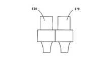
まず、乾燥処理ユニットDRYの構成について説明する。図4は乾燥処理ユニットDRYの構成を説明するための図である。
次に、上記の構成を有する乾燥処理ユニットDRYの処理動作について説明する。なお、以下に説明する乾燥処理ユニットDRYの各構成要素の動作は、図1のメインコントローラ30により制御される。
また、図4に示した乾燥処理ユニットDRYにおいては、洗浄処理用ノズル650と乾燥処理用ノズル670とが別個に設けられているが、図6に示すように、洗浄処理用ノズル650と乾燥処理用ノズル670とを一体に設けてもよい。この場合、基板Wの洗浄処理時または乾燥処理時に洗浄処理用ノズル650および乾燥処理用ノズル670をそれぞれ別々に移動させる必要がないので、駆動機構を単純化することができる。
上記のように、本実施の形態に係る基板処理装置500のインターフェースブロック13においては、フォトレジスト膜の形成された基板Wがインターフェース用搬送機構IFRにより露光装置14に搬入され、露光処理の施された基板Wがインターフェース用搬送機構IFRにより乾燥処理ユニットDRYに搬入される。乾燥処理ユニットDRYにより基板Wの乾燥処理が行われる。
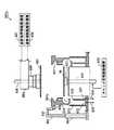
次に、インターフェース用搬送機構IFRについて説明する。図12はインターフェース用搬送機構IFRの構成および動作を説明するための図である。
まず、インターフェース用搬送機構IFRの構成について説明する。図12に示すように、インターフェース用搬送機構IFRの固定台21にはハンド支持台24が±θ方向に回転可能でかつ±Z方向に昇降可能に搭載される。ハンド支持台24は、回転軸25を介して固定台21内のモータM2に連結しており、このモータM2によりハンド支持台24が回転する。ハンド支持台24には、基板Wを水平姿勢で保持する2個のハンドH5,H6が進退可能に上下に設けられる。
上記のように、本実施の形態においては、基板Wを基板載置部PASS9から露光装置14へと搬送する際および乾燥処理ユニットDRYから基板載置部PASS10へと搬送する際には、インターフェース用搬送機構IFRのハンドH5を用い、基板Wを露光装置14から乾燥処理ユニットDRYへと搬送する際にはハンドH6を用いる。すなわち、露光処理後の液体が付着した基板Wの搬送にはハンドH6が用いられ、露光処理前の液体が付着していない基板Wの搬送にはハンドH5が用いられる。そのため、ハンドH5に基板Wの液体が付着することがない。
なお、本実施の形態においては、1台のインターフェース用搬送機構IFRによって、基板載置部PASS9から露光装置14への搬送、露光装置14から乾燥処理ユニットDRYへの搬送および乾燥処理ユニットDRYから基板載置部PASS10への搬送を行っているが、複数のインターフェース用搬送機構IFRを用いて基板Wの搬送を行ってもよい。
(2−1)2流体ノズルを用いた乾燥処理ユニット
第2の実施の形態に係る基板処理装置が第1の実施の形態に係る基板処理装置と異なるのは、乾燥処理ユニットDRYにおいて図4の洗浄処理用ノズル650および乾燥処理用ノズル670の代わりに図13に示すような2流体ノズルが用いられる点である。第2の実施の形態に係る基板処理装置の他の部分の構成は、第1の実施の形態に係る基板処理装置と同様である。
なお、図13の2流体ノズル950を用いた場合においては、2流体ノズル950により基板Wにリンス液を供給しているが、別個のノズルを用いて基板Wにリンス液を供給してもよい。
第2の実施の形態に係る基板処理装置500のインターフェースブロック13においては、フォトレジスト膜の形成された基板Wがインターフェース用搬送機構IFRにより露光装置14に搬入され、露光処理の施された基板Wがインターフェース用搬送機構IFRにより乾燥処理ユニットDRYに搬入される。乾燥処理ユニットDRYにより基板Wの洗浄処理が行われる。この場合、露光処理後に基板Wに付着した水滴残渣、および基板W上の有機膜からの溶出物等は、乾燥処理ユニットDRYにおいて2流体ノズル950から洗浄液と不活性ガスとの混合流体が基板Wに供給されることにより取り除かれる。
本実施の形態においては、反射防止膜用処理ブロック10、レジスト膜用処理ブロック11および現像処理ブロック12が処理部に相当し、インターフェースブロック13が受け渡し部に相当し、塗布ユニットRESが第1の処理ユニットに相当し、乾燥処理ユニットDRY,DRYaが第2の処理ユニットに相当し、エッジ露光部EEWが第3の処理ユニットに相当し、基板載置部PASS9,10が載置部に相当し、第4のセンターロボットCR4が搬送ユニットに相当し、インターフェース用搬送機構IFRが搬送機構に相当する。
10 反射防止膜用処理ブロック
11 レジスト膜用処理ブロック
12 現像処理ブロック
13 インターフェースブロック
14 露光装置
60 キャリア載置台
70 反射防止膜用塗布処理部
80 レジスト膜用塗布処理部
90 現像処理部
95 乾燥処理部
100,101 反射防止膜用熱処理部
110,111 レジスト膜用熱処理部
120,121 現像用熱処理部
311a 液体吐出口
311b 液体導入部
312a 気体吐出口
312b 気体通過部
500 基板処理装置
621 スピンチャック
625 回転軸
636 チャック回転駆動機構
650 洗浄処理用ノズル
670,770,870 乾燥処理用ノズル
682 遮断板
950 2流体ノズル
CR1 第1のセンターロボット
CR2 第2のセンターロボット
CR3 第3のセンターロボット
CR4 第4のセンターロボット
RES 塗布ユニット
EEW エッジ露光部
DRY,DRYa 乾燥処理ユニット
IR インデクサロボット
IFR インターフェース用搬送機構
W 基板
PASS1〜PASS10 基板載置部
Claims (21)
- 液浸法により基板に露光処理を行う露光装置に隣接するように配置される基板処理装置であって、
基板に処理を行うための処理部と、
前記処理部と前記露光装置との間で基板の受け渡しを行うための受け渡し部とを備え、
前記処理部は、前記露光装置による露光処理前の基板に感光性材料からなる感光性膜を形成する第1の処理ユニットを含み、
前記受け渡し部は、前記露光装置による露光処理後に基板の洗浄を行うとともに洗浄後の基板を乾燥させる第2の処理ユニットと、
前記処理部、前記露光装置および前記第2の処理ユニットの間で基板を搬送する搬送手段とを含み、
前記搬送手段は、前記露光装置への基板の搬送および前記露光装置からの基板の搬送を行う搬送機構を含み、
前記搬送機構は、第1および第2の保持手段を有し、前記露光装置への基板の搬送時には前記第1の保持手段により基板を保持し、前記露光装置からの基板の搬送時には前記第2の保持手段により基板を保持することを特徴とする基板処理装置。 - 前記第2の保持手段は前記第1の保持手段よりも下方に設けられたことを特徴とする請求項1記載の基板処理装置。
- 前記第2の処理ユニットは、基板上に不活性ガスを供給することにより基板を乾燥させることを特徴とする請求項1または2記載の基板処理装置。
- 前記受け渡し部は、基板に所定の処理を行う第3の処理ユニットと基板が一時的に載置される載置部とをさらに含み、
前記搬送手段は、前記処理部、前記第3の処理ユニットおよび前記載置部の間で基板を搬送する搬送ユニットをさらに含み、
前記搬送機構は、前記載置部、前記第2の処理ユニットおよび前記露光装置の間で基板を搬送し、前記露光装置から前記第2の処理ユニットに基板を搬送することを特徴とする請求項1〜3のいずれかに記載の基板処理装置。 - 前記第3の処理ユニットは、基板の周縁部を露光するエッジ露光部を含むことを特徴とする請求項4記載の基板処理装置。
- 前記第2の処理ユニットは、
基板を略水平に保持する基板保持手段と、
前記基板保持手段により保持された基板をその基板に垂直な軸の周りで回転させる回転駆動手段と、
前記基板保持手段に保持された基板上に洗浄液を供給する洗浄液供給手段と、
前記洗浄液供給手段により基板上に洗浄液が供給された後に基板上に不活性ガスを供給する不活性ガス供給手段とを備えることを特徴とする請求項1〜5のいずれかに記載の基板処理装置。 - 前記不活性ガス供給手段は、前記洗浄液供給手段により基板上に供給された洗浄液が基板上の中心部から外方へ移動することにより基板上から排除されるように不活性ガスを供給することを特徴とする請求項6記載の基板処理装置。
- 前記第2の処理ユニットは、
前記洗浄液供給手段により洗浄液が供給された後であって前記不活性ガス供給手段により不活性ガスが供給される前に、基板上にリンス液を供給するリンス液供給手段をさらに備えることを特徴とする請求項6記載の基板処理装置。 - 前記不活性ガス供給手段は、前記リンス液供給手段により基板上に供給されたリンス液が基板上の中心部から外方へ移動することにより基板上から排除されるように不活性ガスを供給することを特徴とする請求項8記載の基板処理装置。
- 前記第2の処理ユニットは、液体および気体を含む混合流体を基板に供給する流体ノズルにより基板の洗浄処理を行うことを特徴とする請求項1記載の基板処理装置。
- 前記第2の処理ユニットは、前記流体ノズルから不活性ガスおよび洗浄液を含む混合流体を基板に供給することにより基板の洗浄処理を行うことを特徴とする請求項10記載の基板処理装置。
- 前記第2の処理ユニットは、基板上に不活性ガスを供給することにより基板の乾燥処理を行う不活性ガス供給手段を含むことを特徴とする請求項10または11記載の基板処理装置。
- 前記流体ノズルは前記不活性ガス供給手段として機能することを特徴とする請求項12記載の基板処理装置。
- 前記第2の処理ユニットは、
基板を略水平に保持する基板保持手段と、
前記基板保持手段により保持された基板をその基板に垂直な軸の周りで回転させる回転駆動手段とをさらに含むことを特徴とする請求項12または13記載の基板処理装置。 - 前記第2の処理ユニットは、前記流体ノズルから基板上に供給された混合流体が基板上の中心部から外方へ移動することにより基板上から排除されるように不活性ガスを供給することを特徴とする請求項12〜14のいずれかに記載の基板処理装置。
- 前記第2の処理ユニットは、
前記流体ノズルから混合流体が供給された後であって前記不活性ガス供給手段により前記不活性ガスが供給される前に、基板上にリンス液を供給するリンス液供給手段をさらに含むことを特徴とする請求項12〜14のいずれかに記載の基板処理装置。 - 前記流体ノズルは前記リンス液供給手段として機能することを特徴とする請求項16記載の基板処理装置。
- 前記第2の処理ユニットは、前記リンス液供給手段により基板上に供給されたリンス液が基板上の中心部から外方へ移動することにより基板上から排除されるように不活性ガスを供給することを特徴とする請求項16または17記載の基板処理装置。
- 前記流体ノズルは、液体が流通する液体流路と、気体が流通する気体流路と、前記液体流路に連通して開口する液体吐出口と、前記液体吐出口の近傍に設けられるとともに前記気体流路に連通して開口する気体吐出口とを有することを特徴とする請求項10〜18のいずれかに記載の基板処理装置。
- 第1の処理ユニットを含む処理部と、搬送手段および第2の処理ユニットを含む受け渡し部とを備え、液浸法により基板に露光処理を行う露光装置に隣接するように配置された基板処理装置において基板を処理する方法であって、
前記処理部において前記第1の処理ユニットにより基板に感光性材料からなる感光性膜を形成する工程と、
前記受け渡し部において前記搬送手段により基板を前記処理部から前記露光装置に搬送する工程と、
前記受け渡し部において前記露光装置による露光処理後に基板を前記搬送手段により前記第2の処理ユニットに搬送する工程と、
前記受け渡し部において前記第2の処理ユニットにより基板の洗浄を行う工程と、
前記基板の洗浄を行う工程の後に前記受け渡し部において前記第2の処理ユニットにより基板の乾燥を行う工程と、
前記受け渡し部において前記第2の処理ユニットにより乾燥された基板を前記搬送手段により前記処理部に搬送する工程とを備え、
前記搬送手段は、第1および第2の保持手段を有する搬送機構を含み、
前記搬送手段により基板を前記処理部から前記露光装置に搬送する工程は、前記搬送機構の前記第1の保持手段により基板を保持して前記露光装置に搬送する工程を含み、
前記露光装置による露光処理後に基板を前記搬送手段により前記第2の処理ユニットに搬送する工程は、前記搬送機構の前記第2の保持手段により基板を保持して前記露光装置から搬送する工程を含むことを特徴とする基板処理方法。 - 前記第2の処理ユニットにより基板の洗浄を行う工程は、
前記第2の処理ユニットにおいて液体および気体を含む混合流体を基板に供給する流体ノズルにより基板の洗浄を行う工程を含むことを特徴とする請求項20記載の基板処理方法。
Priority Applications (4)
| Application Number | Priority Date | Filing Date | Title |
|---|---|---|---|
| JP2005216159AJP5008280B2 (ja) | 2004-11-10 | 2005-07-26 | 基板処理装置および基板処理方法 |
| US11/273,465US20060098979A1 (en) | 2004-11-10 | 2005-11-10 | Substrate processing apparatus and substrate processing method |
| CN2005101204401ACN1773376B (zh) | 2004-11-10 | 2005-11-10 | 基板处理装置及基板处理方法 |
| US12/754,872US8496761B2 (en) | 2004-11-10 | 2010-04-06 | Substrate processing apparatus and substrate processing method |
Applications Claiming Priority (5)
| Application Number | Priority Date | Filing Date | Title |
|---|---|---|---|
| JP2004326309 | 2004-11-10 | ||
| JP2004326309 | 2004-11-10 | ||
| JP2005095784 | 2005-03-29 | ||
| JP2005095784 | 2005-03-29 | ||
| JP2005216159AJP5008280B2 (ja) | 2004-11-10 | 2005-07-26 | 基板処理装置および基板処理方法 |
Publications (2)
| Publication Number | Publication Date |
|---|---|
| JP2006310723A JP2006310723A (ja) | 2006-11-09 |
| JP5008280B2true JP5008280B2 (ja) | 2012-08-22 |
Family
ID=36316446
Family Applications (1)
| Application Number | Title | Priority Date | Filing Date |
|---|---|---|---|
| JP2005216159AExpired - LifetimeJP5008280B2 (ja) | 2004-11-10 | 2005-07-26 | 基板処理装置および基板処理方法 |
Country Status (3)
| Country | Link |
|---|---|
| US (2) | US20060098979A1 (ja) |
| JP (1) | JP5008280B2 (ja) |
| CN (1) | CN1773376B (ja) |
Cited By (1)
| Publication number | Priority date | Publication date | Assignee | Title |
|---|---|---|---|---|
| KR20160035995A (ko)* | 2014-09-24 | 2016-04-01 | 램 리써치 코포레이션 | 건조 모듈 내의 이동식 가스 노즐 |
Families Citing this family (16)
| Publication number | Priority date | Publication date | Assignee | Title |
|---|---|---|---|---|
| JP5154008B2 (ja)* | 2004-11-10 | 2013-02-27 | 株式会社Sokudo | 基板処理装置および基板処理方法 |
| JP5008280B2 (ja)* | 2004-11-10 | 2012-08-22 | 株式会社Sokudo | 基板処理装置および基板処理方法 |
| JP4926433B2 (ja)* | 2004-12-06 | 2012-05-09 | 株式会社Sokudo | 基板処理装置および基板処理方法 |
| JP5154006B2 (ja)* | 2004-12-06 | 2013-02-27 | 株式会社Sokudo | 基板処理装置 |
| JP5154007B2 (ja)* | 2004-12-06 | 2013-02-27 | 株式会社Sokudo | 基板処理装置 |
| JP4794232B2 (ja)* | 2004-12-06 | 2011-10-19 | 株式会社Sokudo | 基板処理装置 |
| JP4514657B2 (ja)* | 2005-06-24 | 2010-07-28 | 株式会社Sokudo | 基板処理装置 |
| JP4761907B2 (ja)* | 2005-09-28 | 2011-08-31 | 株式会社Sokudo | 基板処理装置 |
| JP2007201078A (ja)* | 2006-01-25 | 2007-08-09 | Sokudo:Kk | 基板処理装置 |
| JP5132108B2 (ja) | 2006-02-02 | 2013-01-30 | 株式会社Sokudo | 基板処理装置 |
| JP4832201B2 (ja)* | 2006-07-24 | 2011-12-07 | 大日本スクリーン製造株式会社 | 基板処理装置 |
| JP2008060302A (ja)* | 2006-08-31 | 2008-03-13 | Sokudo:Kk | 基板処理装置 |
| JP5779168B2 (ja)* | 2012-12-04 | 2015-09-16 | 東京エレクトロン株式会社 | 周縁部塗布装置、周縁部塗布方法及び周縁部塗布用記録媒体 |
| CN106338418B (zh)* | 2015-07-02 | 2021-07-20 | 生捷科技控股公司 | 分配和混合试剂的系统和方法 |
| JP6577385B2 (ja)* | 2016-02-12 | 2019-09-18 | 株式会社荏原製作所 | 基板保持モジュール、基板処理装置、および基板処理方法 |
| US20220223997A1 (en)* | 2021-01-13 | 2022-07-14 | Zebra Technologies Corporation | User-Installable Wireless Communications Module |
Family Cites Families (108)
| Publication number | Priority date | Publication date | Assignee | Title |
|---|---|---|---|---|
| US3961100A (en)* | 1974-09-16 | 1976-06-01 | Rca Corporation | Method for developing electron beam sensitive resist films |
| JPS5911628A (ja) | 1982-07-12 | 1984-01-21 | Mitsubishi Electric Corp | パタ−ン形成法 |
| US4751170A (en)* | 1985-07-26 | 1988-06-14 | Nippon Telegraph And Telephone Corporation | Silylation method onto surface of polymer membrane and pattern formation process by the utilization of silylation method |
| JPS6381820A (ja)* | 1986-09-25 | 1988-04-12 | Toshiba Corp | レジストパタ−ン形成方法 |
| US5202716A (en)* | 1988-02-12 | 1993-04-13 | Tokyo Electron Limited | Resist process system |
| KR970003907B1 (ko)* | 1988-02-12 | 1997-03-22 | 도오교오 에레구토론 가부시끼 가이샤 | 기판처리 장치 및 기판처리 방법 |
| JP2931820B2 (ja) | 1991-11-05 | 1999-08-09 | 東京エレクトロン株式会社 | 板状体の処理装置及び搬送装置 |
| JPH06124873A (ja)* | 1992-10-09 | 1994-05-06 | Canon Inc | 液浸式投影露光装置 |
| JP3032999B2 (ja) | 1992-11-09 | 2000-04-17 | 東京エレクトロン株式会社 | 処理装置 |
| JP2753930B2 (ja)* | 1992-11-27 | 1998-05-20 | キヤノン株式会社 | 液浸式投影露光装置 |
| US5442415A (en)* | 1994-08-15 | 1995-08-15 | Industrial Technology Research Institute | Armless transparency projector |
| JP2996127B2 (ja)* | 1995-02-17 | 1999-12-27 | 日本電気株式会社 | パターン形成方法 |
| US5788868A (en)* | 1995-09-04 | 1998-08-04 | Dainippon Screen Mfg. Co., Ltd. | Substrate transfer method and interface apparatus |
| TW396490B (en) | 1997-11-14 | 2000-07-01 | Dainippon Screen Mfg | Wafer processor |
| JPH11260686A (ja)* | 1998-03-11 | 1999-09-24 | Toshiba Corp | 露光方法 |
| US6261378B1 (en)* | 1998-03-23 | 2001-07-17 | Tokyo Electron Limited | Substrate cleaning unit and cleaning method |
| WO1999049504A1 (fr) | 1998-03-26 | 1999-09-30 | Nikon Corporation | Procede et systeme d'exposition par projection |
| US6319322B1 (en)* | 1998-07-13 | 2001-11-20 | Tokyo Electron Limited | Substrate processing apparatus |
| JP3642696B2 (ja) | 1999-02-26 | 2005-04-27 | 大日本スクリーン製造株式会社 | 基板保持装置およびそれを用いた基板処理装置 |
| JP2000340544A (ja) | 1999-05-27 | 2000-12-08 | Sharp Corp | 半導体装置の製造方法 |
| US6402400B1 (en)* | 1999-10-06 | 2002-06-11 | Tokyo Electron Limited | Substrate processing apparatus |
| JP4170943B2 (ja) | 1999-10-19 | 2008-10-22 | 東京エレクトロン株式会社 | 基板処理装置 |
| US6402401B1 (en)* | 1999-10-19 | 2002-06-11 | Tokyo Electron Limited | Substrate processing apparatus and substrate processing method |
| KR100348938B1 (ko)* | 1999-12-06 | 2002-08-14 | 한국디엔에스 주식회사 | 포토리소그라피 공정을 위한 반도체 제조장치 |
| JP2001203143A (ja) | 2000-01-20 | 2001-07-27 | Nikon Corp | 基板処理装置 |
| JP3698403B2 (ja)* | 2000-02-28 | 2005-09-21 | 東京エレクトロン株式会社 | 回転式液処理装置 |
| JP4054159B2 (ja)* | 2000-03-08 | 2008-02-27 | 東京エレクトロン株式会社 | 基板処理方法及びその装置 |
| US6634806B2 (en)* | 2000-03-13 | 2003-10-21 | Tokyo Electron Limited | Substrate processing method and substrate processing apparatus |
| JP2001357567A (ja)* | 2000-04-14 | 2001-12-26 | Tdk Corp | 光ディスク原盤の製造方法 |
| JP3559219B2 (ja) | 2000-05-09 | 2004-08-25 | 東京エレクトロン株式会社 | 塗布現像処理システム及び塗布現像処理方法 |
| TW594835B (en)* | 2000-05-09 | 2004-06-21 | Tokyo Electron Ltd | System for coating and developing |
| US7451774B2 (en)* | 2000-06-26 | 2008-11-18 | Applied Materials, Inc. | Method and apparatus for wafer cleaning |
| JP3625755B2 (ja)* | 2000-09-13 | 2005-03-02 | 大日本スクリーン製造株式会社 | 基板処理装置 |
| JP2002148820A (ja)* | 2000-11-15 | 2002-05-22 | Clariant (Japan) Kk | パターン形成方法及びこの方法に使用される処理剤 |
| JP3841641B2 (ja) | 2000-12-27 | 2006-11-01 | 大日本スクリーン製造株式会社 | 基板処理装置 |
| JP4124400B2 (ja)* | 2001-01-19 | 2008-07-23 | 大日本スクリーン製造株式会社 | 基板処理装置 |
| KR100507019B1 (ko)* | 2001-02-07 | 2005-08-09 | 동경 엘렉트론 주식회사 | 무전해 도금 처리 방법 및 무전해 도금 처리 장치 |
| JP2002273360A (ja) | 2001-03-22 | 2002-09-24 | Dainippon Screen Mfg Co Ltd | 基板処理装置 |
| US6558053B2 (en)* | 2001-04-19 | 2003-05-06 | Dainippon Screen Mfg. Co., Ltd. | Substrate processing apparatus |
| TW538472B (en) | 2001-04-27 | 2003-06-21 | Kobe Steel Ltd | Method and system for processing substrate |
| JP3778815B2 (ja) | 2001-06-21 | 2006-05-24 | 大日本スクリーン製造株式会社 | 基板洗浄装置 |
| JP2003007664A (ja)* | 2001-06-22 | 2003-01-10 | Ses Co Ltd | 枚葉式基板洗浄方法および枚葉式基板洗浄装置 |
| JP4053263B2 (ja)* | 2001-08-17 | 2008-02-27 | 株式会社ルネサステクノロジ | 半導体装置の製造方法 |
| US20030045098A1 (en)* | 2001-08-31 | 2003-03-06 | Applied Materials, Inc. | Method and apparatus for processing a wafer |
| US7280883B2 (en)* | 2001-09-06 | 2007-10-09 | Dainippon Screen Mfg. Co., Ltd. | Substrate processing system managing apparatus information of substrate processing apparatus |
| JP2003086479A (ja) | 2001-09-07 | 2003-03-20 | Dainippon Screen Mfg Co Ltd | 基板処理システム、基板処理装置管理方法、基板処理装置、プログラム及び記録媒体 |
| JP3725809B2 (ja)* | 2001-09-19 | 2005-12-14 | 大日本スクリーン製造株式会社 | 基板処理装置および基板処理方法 |
| JP2003093943A (ja)* | 2001-09-26 | 2003-04-02 | Dainippon Screen Mfg Co Ltd | 基板処理装置および基板処理方法 |
| TW561516B (en)* | 2001-11-01 | 2003-11-11 | Tokyo Electron Ltd | Substrate processing apparatus and substrate processing method |
| KR100672632B1 (ko)* | 2001-11-06 | 2007-02-09 | 엘지.필립스 엘시디 주식회사 | 액정표시소자의 약액교환방법 및 그 장치 |
| JP2003205265A (ja) | 2002-01-11 | 2003-07-22 | Tokyo Electron Ltd | 塗布膜形成装置及びその方法 |
| TWI261875B (en)* | 2002-01-30 | 2006-09-11 | Tokyo Electron Ltd | Processing apparatus and substrate processing method |
| KR100469359B1 (ko)* | 2002-02-20 | 2005-02-02 | 엘지.필립스 엘시디 주식회사 | 액정표시소자용 합착 장치 |
| JP4570008B2 (ja)* | 2002-04-16 | 2010-10-27 | 東京エレクトロン株式会社 | 液処理装置および液処理方法 |
| JP4342147B2 (ja)* | 2002-05-01 | 2009-10-14 | 大日本スクリーン製造株式会社 | 基板処理装置 |
| JP2004015023A (ja) | 2002-06-11 | 2004-01-15 | Dainippon Screen Mfg Co Ltd | 基板処理装置およびその方法 |
| US6832863B2 (en)* | 2002-06-11 | 2004-12-21 | Dainippon Screen Mfg. Co., Ltd. | Substrate treating apparatus and method |
| JP3831310B2 (ja) | 2002-07-18 | 2006-10-11 | 東京エレクトロン株式会社 | 処理装置 |
| JP4298238B2 (ja) | 2002-08-27 | 2009-07-15 | 大日本スクリーン製造株式会社 | 基板処理装置および基板処理システム |
| KR100493849B1 (ko)* | 2002-09-30 | 2005-06-08 | 삼성전자주식회사 | 웨이퍼 건조 장치 |
| JP2004134674A (ja)* | 2002-10-11 | 2004-04-30 | Toshiba Corp | 基板処理方法、加熱処理装置、パターン形成方法 |
| JP4702920B2 (ja) | 2002-11-12 | 2011-06-15 | 大日本スクリーン製造株式会社 | 基板処理方法および基板処理装置 |
| US7524771B2 (en)* | 2002-10-29 | 2009-04-28 | Dainippon Screen Mfg. Co., Ltd. | Substrate processing method using alkaline solution and acid solution |
| JP4087328B2 (ja) | 2002-11-28 | 2008-05-21 | 東京エレクトロン株式会社 | 塗布、現像装置及び塗布、現像装置の運転方法 |
| KR100935291B1 (ko)* | 2002-11-28 | 2010-01-06 | 도쿄엘렉트론가부시키가이샤 | 기판 처리 시스템 및 도포 현상 장치 |
| KR20050085026A (ko)* | 2002-12-10 | 2005-08-29 | 가부시키가이샤 니콘 | 광학 소자 및 그 광학 소자를 사용한 투영 노광 장치 |
| KR100505328B1 (ko)* | 2002-12-12 | 2005-07-29 | 엘지.필립스 엘시디 주식회사 | 구리 몰리브덴막에서 몰리브덴 잔사를 제거할 수 있는식각용액 및 그 식각 방법 |
| JP4170864B2 (ja)* | 2003-02-03 | 2008-10-22 | 大日本スクリーン製造株式会社 | 基板処理装置および基板処理装置における基板搬送方法および基板処理方法 |
| TW200424767A (en) | 2003-02-20 | 2004-11-16 | Tokyo Ohka Kogyo Co Ltd | Immersion exposure process-use resist protection film forming material, composite film, and resist pattern forming method |
| JP2004273894A (ja) | 2003-03-11 | 2004-09-30 | Renesas Technology Corp | 半導体集積回路装置の製造方法 |
| JP4307132B2 (ja) | 2003-04-16 | 2009-08-05 | 大日本スクリーン製造株式会社 | 基板処理装置 |
| JP2004342654A (ja) | 2003-05-13 | 2004-12-02 | Dainippon Screen Mfg Co Ltd | 基板処理装置 |
| KR20060009356A (ko)* | 2003-05-15 | 2006-01-31 | 가부시키가이샤 니콘 | 노광 장치 및 디바이스 제조 방법 |
| JP4397646B2 (ja)* | 2003-07-30 | 2010-01-13 | 東京エレクトロン株式会社 | 基板処理装置および基板処理方法 |
| WO2005015627A1 (en)* | 2003-08-07 | 2005-02-17 | Ebara Corporation | Substrate processing apparatus, substrate processing method, and substrate holding apparatus |
| JP4265766B2 (ja) | 2003-08-25 | 2009-05-20 | 東京応化工業株式会社 | 液浸露光プロセス用レジスト保護膜形成用材料、該保護膜形成材料からなるレジスト保護膜、および該レジスト保護膜を用いたレジストパターン形成方法 |
| US7070915B2 (en)* | 2003-08-29 | 2006-07-04 | Tokyo Electron Limited | Method and system for drying a substrate |
| US6873938B1 (en)* | 2003-09-17 | 2005-03-29 | Asml Netherlands B.V. | Adaptive lithographic critical dimension enhancement |
| JP3993549B2 (ja)* | 2003-09-30 | 2007-10-17 | 株式会社東芝 | レジストパターン形成方法 |
| KR20060126949A (ko) | 2003-10-08 | 2006-12-11 | 가부시키가이샤 니콘 | 기판 반송 장치와 기판 반송 방법, 노광 장치와 노광 방법,및 디바이스 제조 방법 |
| JP4194495B2 (ja) | 2004-01-07 | 2008-12-10 | 東京エレクトロン株式会社 | 塗布・現像装置 |
| JP3857692B2 (ja) | 2004-01-15 | 2006-12-13 | 株式会社東芝 | パターン形成方法 |
| JP4220423B2 (ja)* | 2004-03-24 | 2009-02-04 | 株式会社東芝 | レジストパターン形成方法 |
| JP4535489B2 (ja)* | 2004-03-31 | 2010-09-01 | 東京エレクトロン株式会社 | 塗布・現像装置 |
| JP4061284B2 (ja) | 2004-03-31 | 2008-03-12 | 大日本スクリーン製造株式会社 | 基板処理装置 |
| JP4401879B2 (ja) | 2004-07-07 | 2010-01-20 | 東京エレクトロン株式会社 | 基板の回収方法及び基板処理装置 |
| US7259829B2 (en)* | 2004-07-26 | 2007-08-21 | Asml Netherlands B.V. | Lithographic apparatus and device manufacturing method |
| JP2006049757A (ja) | 2004-08-09 | 2006-02-16 | Tokyo Electron Ltd | 基板処理方法 |
| JP4271109B2 (ja) | 2004-09-10 | 2009-06-03 | 東京エレクトロン株式会社 | 塗布、現像装置、レジストパターン形成方法、露光装置及び洗浄装置 |
| JP2006310724A (ja)* | 2004-11-10 | 2006-11-09 | Dainippon Screen Mfg Co Ltd | 基板処理装置および基板処理方法 |
| JP5154008B2 (ja)* | 2004-11-10 | 2013-02-27 | 株式会社Sokudo | 基板処理装置および基板処理方法 |
| JP4463081B2 (ja)* | 2004-11-10 | 2010-05-12 | 大日本スクリーン製造株式会社 | 基板処理装置および基板処理方法 |
| JP5008280B2 (ja)* | 2004-11-10 | 2012-08-22 | 株式会社Sokudo | 基板処理装置および基板処理方法 |
| JP4381285B2 (ja) | 2004-11-11 | 2009-12-09 | 株式会社Sokudo | 基板処理装置および基板処理方法 |
| US7362412B2 (en)* | 2004-11-18 | 2008-04-22 | International Business Machines Corporation | Method and apparatus for cleaning a semiconductor substrate in an immersion lithography system |
| JP5008268B2 (ja) | 2004-12-06 | 2012-08-22 | 株式会社Sokudo | 基板処理装置および基板処理方法 |
| JP4926433B2 (ja) | 2004-12-06 | 2012-05-09 | 株式会社Sokudo | 基板処理装置および基板処理方法 |
| JP4794232B2 (ja)* | 2004-12-06 | 2011-10-19 | 株式会社Sokudo | 基板処理装置 |
| JP5154007B2 (ja) | 2004-12-06 | 2013-02-27 | 株式会社Sokudo | 基板処理装置 |
| JP5154006B2 (ja) | 2004-12-06 | 2013-02-27 | 株式会社Sokudo | 基板処理装置 |
| US7245348B2 (en)* | 2005-01-21 | 2007-07-17 | Tokyo Electron Limited | Coating and developing system and coating and developing method with antireflection film and an auxiliary block for inspection and cleaning |
| JP4622571B2 (ja)* | 2005-02-18 | 2011-02-02 | セイコーエプソン株式会社 | 液体噴射装置 |
| DE102005017516B3 (de)* | 2005-04-15 | 2007-01-25 | Infineon Technologies Ag | Fotolithografische Abbildungseinrichtung und Vorrichtung zum Erzeugen einer Beleuchtungsverteilung |
| JP4514657B2 (ja)* | 2005-06-24 | 2010-07-28 | 株式会社Sokudo | 基板処理装置 |
| JP4522329B2 (ja)* | 2005-06-24 | 2010-08-11 | 株式会社Sokudo | 基板処理装置 |
| US7766565B2 (en)* | 2005-07-01 | 2010-08-03 | Sokudo Co., Ltd. | Substrate drying apparatus, substrate cleaning apparatus and substrate processing system |
| JP4761907B2 (ja) | 2005-09-28 | 2011-08-31 | 株式会社Sokudo | 基板処理装置 |
| JP5192206B2 (ja)* | 2007-09-13 | 2013-05-08 | 株式会社Sokudo | 基板処理装置および基板処理方法 |
- 2005
- 2005-07-26JPJP2005216159Apatent/JP5008280B2/janot_activeExpired - Lifetime
- 2005-11-10CNCN2005101204401Apatent/CN1773376B/zhactiveActive
- 2005-11-10USUS11/273,465patent/US20060098979A1/ennot_activeAbandoned
- 2010
- 2010-04-06USUS12/754,872patent/US8496761B2/enactiveActive
Cited By (2)
| Publication number | Priority date | Publication date | Assignee | Title |
|---|---|---|---|---|
| KR20160035995A (ko)* | 2014-09-24 | 2016-04-01 | 램 리써치 코포레이션 | 건조 모듈 내의 이동식 가스 노즐 |
| KR102479165B1 (ko)* | 2014-09-24 | 2022-12-19 | 램 리써치 코포레이션 | 건조 모듈 내의 이동식 가스 노즐 |
Also Published As
| Publication number | Publication date |
|---|---|
| US8496761B2 (en) | 2013-07-30 |
| US20100190116A1 (en) | 2010-07-29 |
| CN1773376A (zh) | 2006-05-17 |
| US20060098979A1 (en) | 2006-05-11 |
| JP2006310723A (ja) | 2006-11-09 |
| CN1773376B (zh) | 2010-06-23 |
Similar Documents
| Publication | Publication Date | Title |
|---|---|---|
| JP5154008B2 (ja) | 基板処理装置および基板処理方法 | |
| JP4845463B2 (ja) | 基板処理装置 | |
| JP4926433B2 (ja) | 基板処理装置および基板処理方法 | |
| KR100758623B1 (ko) | 기판처리 장치 및 기판처리 방법 | |
| JP4667252B2 (ja) | 基板処理装置 | |
| JP5154007B2 (ja) | 基板処理装置 | |
| JP4771816B2 (ja) | 基板処理装置 | |
| JP4832201B2 (ja) | 基板処理装置 | |
| JP5008280B2 (ja) | 基板処理装置および基板処理方法 | |
| JP5008268B2 (ja) | 基板処理装置および基板処理方法 | |
| JP2007214365A (ja) | 基板処理装置 | |
| JP4514657B2 (ja) | 基板処理装置 | |
| JP5154006B2 (ja) | 基板処理装置 | |
| JP2007201078A (ja) | 基板処理装置 | |
| JP4794232B2 (ja) | 基板処理装置 | |
| JP2007201077A (ja) | 基板処理装置 | |
| JP2007189139A (ja) | 基板処理装置 | |
| CN100535757C (zh) | 基板处理装置 | |
| JP4753641B2 (ja) | 基板処理システム | |
| JP2007208021A (ja) | 基板処理装置および基板処理方法 | |
| JP4579029B2 (ja) | 基板処理装置 | |
| JP2007012998A (ja) | 基板洗浄装置およびそれを備えた基板処理システム | |
| JP2007036121A (ja) | 基板処理装置 |
Legal Events
| Date | Code | Title | Description |
|---|---|---|---|
| A711 | Notification of change in applicant | Free format text:JAPANESE INTERMEDIATE CODE: A712 Effective date:20070129 | |
| A621 | Written request for application examination | Free format text:JAPANESE INTERMEDIATE CODE: A621 Effective date:20070919 | |
| A131 | Notification of reasons for refusal | Free format text:JAPANESE INTERMEDIATE CODE: A131 Effective date:20100706 | |
| A521 | Request for written amendment filed | Free format text:JAPANESE INTERMEDIATE CODE: A523 Effective date:20100831 | |
| A02 | Decision of refusal | Free format text:JAPANESE INTERMEDIATE CODE: A02 Effective date:20110118 | |
| A521 | Request for written amendment filed | Free format text:JAPANESE INTERMEDIATE CODE: A523 Effective date:20110413 | |
| A911 | Transfer to examiner for re-examination before appeal (zenchi) | Free format text:JAPANESE INTERMEDIATE CODE: A911 Effective date:20110512 | |
| A912 | Re-examination (zenchi) completed and case transferred to appeal board | Free format text:JAPANESE INTERMEDIATE CODE: A912 Effective date:20110603 | |
| A521 | Request for written amendment filed | Free format text:JAPANESE INTERMEDIATE CODE: A523 Effective date:20120425 | |
| A01 | Written decision to grant a patent or to grant a registration (utility model) | Free format text:JAPANESE INTERMEDIATE CODE: A01 | |
| A61 | First payment of annual fees (during grant procedure) | Free format text:JAPANESE INTERMEDIATE CODE: A61 Effective date:20120529 | |
| R150 | Certificate of patent or registration of utility model | Free format text:JAPANESE INTERMEDIATE CODE: R150 Ref document number:5008280 Country of ref document:JP Free format text:JAPANESE INTERMEDIATE CODE: R150 | |
| FPAY | Renewal fee payment (event date is renewal date of database) | Free format text:PAYMENT UNTIL: 20150608 Year of fee payment:3 | |
| S533 | Written request for registration of change of name | Free format text:JAPANESE INTERMEDIATE CODE: R313533 | |
| R350 | Written notification of registration of transfer | Free format text:JAPANESE INTERMEDIATE CODE: R350 | |
| R250 | Receipt of annual fees | Free format text:JAPANESE INTERMEDIATE CODE: R250 | |
| R250 | Receipt of annual fees | Free format text:JAPANESE INTERMEDIATE CODE: R250 | |
| R250 | Receipt of annual fees | Free format text:JAPANESE INTERMEDIATE CODE: R250 | |
| R250 | Receipt of annual fees | Free format text:JAPANESE INTERMEDIATE CODE: R250 | |
| R250 | Receipt of annual fees | Free format text:JAPANESE INTERMEDIATE CODE: R250 | |
| R250 | Receipt of annual fees | Free format text:JAPANESE INTERMEDIATE CODE: R250 | |
| R250 | Receipt of annual fees | Free format text:JAPANESE INTERMEDIATE CODE: R250 | |
| R250 | Receipt of annual fees | Free format text:JAPANESE INTERMEDIATE CODE: R250 | |
| R250 | Receipt of annual fees | Free format text:JAPANESE INTERMEDIATE CODE: R250 | |
| R250 | Receipt of annual fees | Free format text:JAPANESE INTERMEDIATE CODE: R250 |