JP5008026B2 - Display device with input function - Google Patents
Display device with input functionDownload PDFInfo
- Publication number
- JP5008026B2 JP5008026B2JP2007019139AJP2007019139AJP5008026B2JP 5008026 B2JP5008026 B2JP 5008026B2JP 2007019139 AJP2007019139 AJP 2007019139AJP 2007019139 AJP2007019139 AJP 2007019139AJP 5008026 B2JP5008026 B2JP 5008026B2
- Authority
- JP
- Japan
- Prior art keywords
- liquid crystal
- electrode
- display device
- substrate
- light
- Prior art date
- Legal status (The legal status is an assumption and is not a legal conclusion. Google has not performed a legal analysis and makes no representation as to the accuracy of the status listed.)
- Active
Links
Images


Classifications
- G—PHYSICS
- G06—COMPUTING OR CALCULATING; COUNTING
- G06F—ELECTRIC DIGITAL DATA PROCESSING
- G06F3/00—Input arrangements for transferring data to be processed into a form capable of being handled by the computer; Output arrangements for transferring data from processing unit to output unit, e.g. interface arrangements
- G06F3/01—Input arrangements or combined input and output arrangements for interaction between user and computer
- G06F3/03—Arrangements for converting the position or the displacement of a member into a coded form
- G06F3/041—Digitisers, e.g. for touch screens or touch pads, characterised by the transducing means
- G06F3/044—Digitisers, e.g. for touch screens or touch pads, characterised by the transducing means by capacitive means
- G06F3/0443—Digitisers, e.g. for touch screens or touch pads, characterised by the transducing means by capacitive means using a single layer of sensing electrodes
- G—PHYSICS
- G06—COMPUTING OR CALCULATING; COUNTING
- G06F—ELECTRIC DIGITAL DATA PROCESSING
- G06F3/00—Input arrangements for transferring data to be processed into a form capable of being handled by the computer; Output arrangements for transferring data from processing unit to output unit, e.g. interface arrangements
- G06F3/01—Input arrangements or combined input and output arrangements for interaction between user and computer
- G06F3/03—Arrangements for converting the position or the displacement of a member into a coded form
- G06F3/041—Digitisers, e.g. for touch screens or touch pads, characterised by the transducing means
- G06F3/0412—Digitisers structurally integrated in a display
- G—PHYSICS
- G02—OPTICS
- G02F—OPTICAL DEVICES OR ARRANGEMENTS FOR THE CONTROL OF LIGHT BY MODIFICATION OF THE OPTICAL PROPERTIES OF THE MEDIA OF THE ELEMENTS INVOLVED THEREIN; NON-LINEAR OPTICS; FREQUENCY-CHANGING OF LIGHT; OPTICAL LOGIC ELEMENTS; OPTICAL ANALOGUE/DIGITAL CONVERTERS
- G02F1/00—Devices or arrangements for the control of the intensity, colour, phase, polarisation or direction of light arriving from an independent light source, e.g. switching, gating or modulating; Non-linear optics
- G02F1/01—Devices or arrangements for the control of the intensity, colour, phase, polarisation or direction of light arriving from an independent light source, e.g. switching, gating or modulating; Non-linear optics for the control of the intensity, phase, polarisation or colour
- G02F1/13—Devices or arrangements for the control of the intensity, colour, phase, polarisation or direction of light arriving from an independent light source, e.g. switching, gating or modulating; Non-linear optics for the control of the intensity, phase, polarisation or colour based on liquid crystals, e.g. single liquid crystal display cells
- G02F1/133—Constructional arrangements; Operation of liquid crystal cells; Circuit arrangements
- G02F1/1333—Constructional arrangements; Manufacturing methods
- G02F1/13338—Input devices, e.g. touch panels
- G—PHYSICS
- G02—OPTICS
- G02F—OPTICAL DEVICES OR ARRANGEMENTS FOR THE CONTROL OF LIGHT BY MODIFICATION OF THE OPTICAL PROPERTIES OF THE MEDIA OF THE ELEMENTS INVOLVED THEREIN; NON-LINEAR OPTICS; FREQUENCY-CHANGING OF LIGHT; OPTICAL LOGIC ELEMENTS; OPTICAL ANALOGUE/DIGITAL CONVERTERS
- G02F1/00—Devices or arrangements for the control of the intensity, colour, phase, polarisation or direction of light arriving from an independent light source, e.g. switching, gating or modulating; Non-linear optics
- G02F1/01—Devices or arrangements for the control of the intensity, colour, phase, polarisation or direction of light arriving from an independent light source, e.g. switching, gating or modulating; Non-linear optics for the control of the intensity, phase, polarisation or colour
- G02F1/13—Devices or arrangements for the control of the intensity, colour, phase, polarisation or direction of light arriving from an independent light source, e.g. switching, gating or modulating; Non-linear optics for the control of the intensity, phase, polarisation or colour based on liquid crystals, e.g. single liquid crystal display cells
- G02F1/133—Constructional arrangements; Operation of liquid crystal cells; Circuit arrangements
- G02F1/1333—Constructional arrangements; Manufacturing methods
- G02F1/1335—Structural association of cells with optical devices, e.g. polarisers or reflectors
- G02F1/133528—Polarisers
- G—PHYSICS
- G02—OPTICS
- G02F—OPTICAL DEVICES OR ARRANGEMENTS FOR THE CONTROL OF LIGHT BY MODIFICATION OF THE OPTICAL PROPERTIES OF THE MEDIA OF THE ELEMENTS INVOLVED THEREIN; NON-LINEAR OPTICS; FREQUENCY-CHANGING OF LIGHT; OPTICAL LOGIC ELEMENTS; OPTICAL ANALOGUE/DIGITAL CONVERTERS
- G02F1/00—Devices or arrangements for the control of the intensity, colour, phase, polarisation or direction of light arriving from an independent light source, e.g. switching, gating or modulating; Non-linear optics
- G02F1/01—Devices or arrangements for the control of the intensity, colour, phase, polarisation or direction of light arriving from an independent light source, e.g. switching, gating or modulating; Non-linear optics for the control of the intensity, phase, polarisation or colour
- G02F1/13—Devices or arrangements for the control of the intensity, colour, phase, polarisation or direction of light arriving from an independent light source, e.g. switching, gating or modulating; Non-linear optics for the control of the intensity, phase, polarisation or colour based on liquid crystals, e.g. single liquid crystal display cells
- G02F1/133—Constructional arrangements; Operation of liquid crystal cells; Circuit arrangements
- G02F1/1333—Constructional arrangements; Manufacturing methods
- G02F1/1335—Structural association of cells with optical devices, e.g. polarisers or reflectors
- G02F1/13363—Birefringent elements, e.g. for optical compensation
- G—PHYSICS
- G06—COMPUTING OR CALCULATING; COUNTING
- G06F—ELECTRIC DIGITAL DATA PROCESSING
- G06F3/00—Input arrangements for transferring data to be processed into a form capable of being handled by the computer; Output arrangements for transferring data from processing unit to output unit, e.g. interface arrangements
- G06F3/01—Input arrangements or combined input and output arrangements for interaction between user and computer
- G06F3/03—Arrangements for converting the position or the displacement of a member into a coded form
- G06F3/041—Digitisers, e.g. for touch screens or touch pads, characterised by the transducing means
- G06F3/044—Digitisers, e.g. for touch screens or touch pads, characterised by the transducing means by capacitive means
- G06F3/0445—Digitisers, e.g. for touch screens or touch pads, characterised by the transducing means by capacitive means using two or more layers of sensing electrodes, e.g. using two layers of electrodes separated by a dielectric layer
Landscapes
- Engineering & Computer Science (AREA)
- Physics & Mathematics (AREA)
- Theoretical Computer Science (AREA)
- General Engineering & Computer Science (AREA)
- General Physics & Mathematics (AREA)
- Nonlinear Science (AREA)
- Human Computer Interaction (AREA)
- Crystallography & Structural Chemistry (AREA)
- Optics & Photonics (AREA)
- Chemical & Material Sciences (AREA)
- Mathematical Physics (AREA)
- Liquid Crystal (AREA)
- Devices For Indicating Variable Information By Combining Individual Elements (AREA)
- Position Input By Displaying (AREA)
- Switches That Are Operated By Magnetic Or Electric Fields (AREA)
Description
Translated fromJapanese本発明は、例えばタッチパネルのような入力機能が付加された入力機能付表示装置に関する。 The present invention relates to a display device with an input function to which an input function such as a touch panel is added.
近年、パーソナルデジタルアシスタント(PDA)、パーソナルコンピュータなどの小型情報電子機器の普及に伴い、表示画面上に指やペンなどの物体を接触させることにより入力操作を行う、いわゆるタッチパネル機能が付加された表示装置が広く利用されている。このようなタッチパネルにおいて、指などの接触位置を検出する方法として静電容量方式がある(例えば、特許文献1、2参照)。
静電容量方式は、人間が指で表示面に触れることで形成された静電容量を介して微弱な電流を流し、この電流量から接触位置の検出を行う方式である。ここで、静電容量方式では、平面状に形成された検出電極と検出電極上に積層された誘電体膜とを用いており、誘電体膜を指などで触れることで静電容量を形成している。In recent years, with the spread of small information electronic devices such as personal digital assistants (PDAs) and personal computers, a display with a so-called touch panel function that performs an input operation by bringing an object such as a finger or a pen into contact with the display screen is added. The device is widely used. In such a touch panel, there is a capacitance method as a method for detecting a contact position of a finger or the like (see, for example,
The capacitance method is a method in which a weak current is passed through a capacitance formed by a person touching a display surface with a finger, and a contact position is detected from this amount of current. Here, the capacitance method uses a detection electrode formed in a planar shape and a dielectric film laminated on the detection electrode, and the capacitance is formed by touching the dielectric film with a finger or the like. ing.
このような静電容量方式を用いたタッチパネル機能付きの液晶表示装置では、液晶層を駆動するために一対の電極間に供給している駆動信号によって発生した電界が検出電極に到達することで、この電界成分がノイズとなって接触位置の検出精度が低くなるという問題がある。ここで、前者のタッチパネル機能付きの液晶表示装置では、駆動信号から生成された信号により発生したノイズを除去することが図られている。
しかしながら、上記従来のタッチパネル機能付きの液晶表示装置においても、以下の課題が残されている。すなわち、従来のタッチパネル機能付きの液晶表示装置では、ノイズを除去する信号を生成するために複雑なシステムが必要であるという問題がある。 However, the following problems remain in the conventional liquid crystal display device with a touch panel function. That is, the conventional liquid crystal display device with a touch panel function has a problem that a complicated system is required to generate a signal for removing noise.
本発明は、上記従来の問題に鑑みてなされたもので、複雑なシステムを要することなくノイズの影響を抑制できる入力機能付表示装置を提供することを目的とする。 The present invention has been made in view of the above-described conventional problems, and an object thereof is to provide a display device with an input function capable of suppressing the influence of noise without requiring a complicated system.
本発明は、上記課題を解決するために以下の構成を採用した。すなわち、本発明にかかる入力機能付表示装置は、液晶層を駆動する一対の電極が設けられた第1基板と、該第1基板と液晶層を介して対向配置され、該液晶装置側に、電位が固定されると共に、ストライプ状に配置された複数の複屈折構造体を有するシールド導体を備える第2基板と、第2基板の外面に積層して設けられた検出電極及び誘電体膜と、該誘電体膜を介して検出電極との間に形成される静電容量の形成位置を検出する検出手段とを備え、シールド導体が、該シールド導体に入射した光に対し、複屈折構造体の延在方向と略直交する偏光方向を有する偏光成分を透過させ、複屈折構造体の延在方向と略平行な偏光方向を有する偏光成分を遮断する。The present invention employs the following configuration in order to solve theabove problems. That is, the display device with an input function according to the present invention includes a first substrate in which a pair of electrodes for driving the liquid crystal layer is provided, it is oppositely arranged with said first substrateand the liquid crystallayer, in the liquid crystal device side A second substrate includinga shield conductor having a plurality of birefringent structures arranged in a stripe shape and having a fixed potential; a detection electrode and a dielectric film provided on the outer surface ofthe second substrate; , and detecting means for detecting a formation position of the electrostatic capacitance formed between thedetection electrodethrough the dielectric film,the shield conductor, for light incident on the shield conductor, birefringence structure A polarized light component having a polarization direction substantially orthogonal to the extending direction of the body is transmitted, and a polarized light component having a polarization direction substantially parallel to the extending direction of the birefringent structure is blocked .
この発明では、第2基板の液晶層側にシールド導体を設けることで、第2基板を大きく厚くせずに複雑なシステムを要することなく液晶層の駆動信号によるノイズの影響を抑制し、表示面への接触位置の検出精度が向上する。また、液晶層と近接して設けられているシールド導体が偏光板として機能することで、液晶層を透過してからシールド導体に入射するまでの光の偏光状態の変化が小さくなるので、コントラストが向上する。
すなわち、一対の電極に液晶層の駆動信号を供給することによって第2基板に向けて発生する電界が、シールド導体により遮断される。このため、一対の電極と検出電極との間でカップリングが発生することを防止できる。ここで、第1基板に液晶層を駆動する一対の電極が設けられており、一対の電極とシールド導体との距離が十分に確保されている。そのため、液晶層の駆動信号によって発生してシールド導体に向かう電界の強度は、いわゆる縦電界方式の電極構造を採用する場合と比較して小さくなる。これにより、シールド導体による電界の遮断がより効果的に行われる。したがって、複雑なシステムを別途設けずに第2基板を大幅に厚くすることなく、一対の電極と検出電極とのカップリングを防止して駆動信号によるノイズの影響が抑制される。また、シールド導体を第2基板に一体的に形成して第2基板を大きく厚くしないことで、十分な透過率を確保できる。
また、シールド導体と検出電極との間が十分に離間しているため、シールド導体と検出電極との間に容量成分が形成されることを防止できる。
そして、シールド導体に入射した光は、複屈折構造体の延在方向とほぼ直交する偏光方向を有する偏光成分がシールド導体を透過すると共に延在方向とほぼ平行な偏光方向を有する偏光成分がシールド導体により遮断される。このため、シールド導体は、偏光板として機能する。ここで、第2基板の外面側に偏光板を配置する場合と比較して偏光板として機能するシールド導体が液晶層と近接して配置されているため、液晶層を透過してからシールド導体または偏光板に入射するまでに散乱や複屈折に起因した光の偏光状態の変化量が小さくなる。これにより、シールド導体による偏光光の透過または遮断を精度よく行え、コントラストの向上が図れる。また、偏光板として機能するシールド導体を第2基板に形成することにより、光軸合わせを精度よく行える。In this invention, by providing a shield conductor on the liquid crystal layer side of the second substrate, the influence of noise due to the drive signal of the liquid crystal layer is suppressed without requiring a complicated system without making the second substrate large and thick, and the display surface The detection accuracy of the contact position is improved. In addition, since the shield conductor provided in the vicinity of the liquid crystal layer functions as a polarizing plate, the change in the polarization state of light from the transmission through the liquid crystal layer to the incidence on the shield conductor is reduced, so that the contrast is reduced. improves.
That is, the electric field generated toward the second substrate by supplying the liquid crystal layer drive signal to the pair of electrodes is blocked by the shield conductor. For this reason, it can prevent that coupling generate | occur | produces between a pair of electrode and a detection electrode. Here, a pair of electrodes for driving the liquid crystal layer is provided on the first substrate, and a sufficient distance between the pair of electrodes and the shield conductor is ensured. Therefore, the intensity of the electric field generated by the driving signal of the liquid crystal layer and directed to the shield conductor is smaller than that in the case where a so-called vertical electric field type electrode structure is adopted. Thereby, electric field interruption by the shield conductor is performed more effectively. Therefore, the coupling between the pair of electrodes and the detection electrodes is prevented and the influence of noise due to the drive signal is suppressed without significantly increasing the thickness of the second substrate without separately providing a complicated system. Moreover, sufficient transmittance can be ensured by forming the shield conductor integrally with the second substrate and making the second substrate not thick.
Further, since the shield conductor and the detection electrode are sufficiently separated from each other, it is possible to prevent a capacitance component from being formed between the shield conductor and the detection electrode.
The light incident on the shield conductor is shielded by the polarization component having a polarization direction substantially orthogonal to the extending direction of the birefringent structure and the polarization component having a polarization direction substantially parallel to the extending direction. Cut off by conductor. For this reason, the shield conductor functions as a polarizing plate. Here, since the shield conductor functioning as a polarizing plate is disposed close to the liquid crystal layer as compared with the case where the polarizing plate is disposed on the outer surface side of the second substrate, the shield conductor or The amount of change in the polarization state of light due to scattering and birefringence becomes small before entering the polarizing plate. Thus, the polarized light can be transmitted or blocked with high accuracy by the shield conductor, and the contrast can be improved. Further, by forming a shield conductor functioning as a polarizing plate on the second substrate, optical axis alignment can be performed with high accuracy.
また、本発明にかかる入力機能付表示装置は、シールド導体が、遮光膜を構成する被覆部を備えることが好ましい。
この発明では、シールド導体が遮光膜を兼ねることにより、部品点数を削減して製造工程の簡略化が図れる。The input-capable display device according to the presentinvention Rudo conductor is preferably provided with a coating portion constituting the light-shielding film.
In this invention, since the shield conductor also serves as the light shielding film, the number of parts can be reduced and the manufacturing process can be simplified.
また、本発明にかかる入力機能付表示装置は、シールド導体が、光反射性材料で構成されていることが好ましい。
この発明では、シールド導体に入射した光のうちシールド導体によって遮断される光を反射することで、第2基板の光の吸収による加熱を抑制できる。The input-capable display device according to the presentinvention Rudo conductors, it is preferably composed of a light reflective material.
In this invention, the heat by absorption of the light of the 2nd board | substrate can be suppressed by reflecting the light interrupted | blocked by the shield conductor among the light which injected into the shield conductor.
また、本発明にかかる入力機能付表示装置は、シールド導体が、光吸収性材料で構成されていることが好ましい。
この発明では、シールド導体に入射した光のうち遮断される光を吸収することで、反射によるコントラストの低下を抑制できる。
The input-capable display device according to the presentinvention Rudo conductors, it is preferably composed of a light absorbing material.
In this invention, by absorbing the light that is blocked out of the light incident on the shield conductor, it is possible to suppress a decrease in contrast due to reflection.
[第1の実施形態]
以下、本発明における入力機能付表示装置の第1の実施形態を、図面に基づいて説明する。なお、以下の説明に用いる各図面では、各部材を認識可能な大きさとするために縮尺を適宜変更している。ここで、図1は入力機能付液晶表示装置の概略断面図、図2は図1の等価回路図、図3はサブ画素領域を示す平面構成図、図4は図3のA−A矢視断面図である。[First Embodiment]
Hereinafter, a display device with an input function according to a first embodiment of the present invention will be described with reference to the drawings. In each drawing used in the following description, the scale is appropriately changed to make each member a recognizable size. 1 is a schematic cross-sectional view of the liquid crystal display device with an input function, FIG. 2 is an equivalent circuit diagram of FIG. 1, FIG. 3 is a plan view showing a sub-pixel region, and FIG. 4 is an AA view of FIG. It is sectional drawing.
〔入力機能付表示装置〕
本実施形態における入力機能付液晶表示装置(入力機能付表示装置)1は、透過型のカラー液晶表示装置であって、R(赤)、G(緑)、B(青)の各色光を出力する3個のサブ画素領域で1個の画素を構成する液晶表示装置である。ここで、表示を構成する最小単位となる表示領域を「サブ画素領域」と称する。[Display device with input function]
A liquid crystal display device with an input function (display device with an input function) 1 according to the present embodiment is a transmissive color liquid crystal display device and outputs light of each color of R (red), G (green), and B (blue). This is a liquid crystal display device in which one pixel is constituted by three sub-pixel regions. Here, the display area which is the minimum unit constituting the display is referred to as a “sub-pixel area”.
最初に、本実施形態における入力機能付液晶表示装置1の概略構成について説明する。
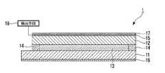
本実施形態における入力機能付液晶表示装置1は、図1に示すように、アクティブマトリックス基板である素子基板(第1基板)11と、素子基板11と対向配置された対向基板(第2基板)12と、素子基板11及び対向基板12に挟持された液晶層13とを備えており、素子基板11の外面側(液晶層13から離間する側)から照明光を照射する構成となっている。
また、入力機能付液晶表示装置1は、素子基板11と対向基板12とが対向する対向領域の外周部に設けられた平面視でほぼ矩形の枠状のシール材14を有しており、このシール材によって素子基板11と対向基板12とが貼り合わされている。そして、入力機能付液晶表示装置1のうちシール材14の内側に、画像表示領域が形成される。
さらに、入力機能付液晶表示装置1は、対向基板12の外面側に設けられた検出電極15と、素子基板11の外面側に設けられた偏光板16及び検出電極15の外面側に設けられた誘電体膜17と、誘電体膜17を介して検出電極15との間に形成される静電容量の形成位置を検出する検出手段18とを備えている。First, a schematic configuration of the liquid
As shown in FIG. 1, the liquid
In addition, the liquid
Further, the liquid
入力機能付液晶表示装置1の画像表示領域には、図2に示すように、複数のサブ画素領域がマトリックス状に配置されている。この複数のサブ画素領域のそれぞれには、画素電極(一方の電極)21と、画素電極21をスイッチング制御するためのTFT(Thin Film Transistor:薄膜トランジスタ)素子22とが形成されている。また、画像表示領域には、複数のデータ線23及び走査線24が格子状に配置されている。
TFT素子22は、ソースがデータ線23に接続され、ゲートが走査線24に接続され、ドレインが画素電極21に接続されている。In the image display area of the liquid
The
データ線23は、入力機能付液晶表示装置1に設けられた駆動回路(図示略)から供給される画像信号S1、S2、…、Snを各サブ画素領域に供給する構成となっている。ここで、データ線23は、画像信号S1〜Snをこの順で線順次で供給してもよく、互いに隣接する複数のデータ線23同士に対してグループごとに供給してもよい。
走査線24は、入力機能付液晶表示装置1に設けられた駆動回路(図示略)から供給される走査信号G1、G2、…、Gmを各サブ画素領域に供給する構成となっている。ここで、走査線24は、走査信号G1〜Gmを所定のタイミングでパルス的に線順次で供給する。The
The
また、入力機能付液晶表示装置1は、スイッチング素子であるTFT素子22が走査信号G1〜Gmの入力により一定期間だけオン状態とされることで、データ線23から供給される画像信号S1〜Snが所定のタイミングで画素電極21に書き込まれる構成となっている。そして、画素電極21を介して液晶に書き込まれた所定レベルの画像信号S1〜Snは、画素電極21と後述する共通電極(他方の電極)43との間で一定期間保持される。 Further, in the liquid
次に、入力機能付液晶表示装置1の詳細な構成について、図3及び図4を参照しながら説明する。なお、図3では、対向基板12の図示を省略している。また、図3において、平面視でほぼ矩形状のサブ画素領域の長軸方向をX軸方向、短軸方向をY軸方向とする。
素子基板11は、図4に示すように、例えばガラスや石英、プラスチックなどの透光性材料からなる基板本体31と、基板本体31の内側(液晶層13側)から順次積層された下地保護膜32、ゲート絶縁膜33、第1層間絶縁膜34、第2層間絶縁膜35、第3層間絶縁膜36及び配向膜37とを備えている。
また、素子基板11は、下地保護膜32の内側の表面に配置された半導体層41と、ゲート絶縁膜33の内側の表面に配置された走査線24と、第1層間絶縁膜34の内側の表面に配置されたデータ線23及び接続電極42と、第2層間絶縁膜35の内側の表面に配置された共通電極43と、第3層間絶縁膜36の内側の表面に配置された画素電極21とを備えている。Next, a detailed configuration of the liquid
As shown in FIG. 4, the
The
下地保護膜32は、例えばSiO2(酸化シリコン)などの透光性のシリコン酸化物で構成されており、基板本体31を被覆している。なお、下地保護膜32は、SiO2に限らず、SiN(窒化シリコン)やSiON(酸窒化シリコン)、セラミックス薄膜などの絶縁材料で構成してもよい。
ゲート絶縁膜33は、例えばSiO2などの透光性材料で構成されており、下地保護膜32上に形成された半導体層41を覆うように設けられている。
第1層間絶縁膜34は、例えばSiO2などの透光性材料で構成されており、ゲート絶縁膜33及びゲート絶縁膜33上に形成された走査線24を覆うように設けられている。
第2層間絶縁膜35は、例えばアクリルなどの透光性材料で構成されており、第1層間絶縁膜34及び第1層間絶縁膜34上に形成されたデータ線23及び接続電極42を覆うように設けられている。
第3層間絶縁膜36は、例えばSiNなどの透光性材料で構成されており、第2層間絶縁膜35の内側の表面に形成された共通電極43を覆うように設けられている。
配向膜37は、例えばポリイミドなどの樹脂材料で構成されており、第3層間絶縁膜36上に形成された画素電極21を覆うように設けられている。また、配向膜37の表面には、図3に示すサブ画素領域の短軸方向(Y軸方向)を配向方向とする配向処理が施されている。The base
The
The first
The second
The third
The
半導体層41は、図3及び図4に示すように平面視でほぼL字状であって、平面視でゲート絶縁膜33を介して走査線24と重なる領域の一部を含んで形成され、ポリシリコンなどの半導体で構成されている。そして、半導体層41には、平面視でゲート絶縁膜33を介して走査線24と重なる領域にチャネル領域41aが設けられている。
また、半導体層41は、不純物イオンを打ち込むことによって形成されたソース領域41b及びドレイン領域41cを有している。そして、半導体層41を主体としてTFT素子22が構成される。なお、チャネル領域41aは、ポリシリコンに不純物イオンを打ち込まないことによって形成される。ここで、半導体層41は、ソース領域及びドレイン領域に不純物濃度が相対的に高い高濃度領域と相対的に低い低濃度(LDD(Lightly Doped Drain))領域とを形成したLDD構造としてもよい。The
The
走査線24は、平面視でほぼ矩形状のサブ画素領域の短軸方向(Y軸方向)に沿って配置されており、例えばAl(アルミニウム)などの金属材料で構成されている。また、走査線24のうちゲート絶縁膜33を介してチャネル領域41aと対向配置する部分は、ゲート電極として機能する。
データ線23は、平面視でサブ画素領域の長軸方向(X軸方向)に沿って配置されており、例えばAlなどの金属材料で構成されている。また、データ線23は、ゲート絶縁膜33及び第1層間絶縁膜34を貫通するコンタクトホールH1を介して半導体層41のソース領域41bに接続されている。すなわち、データ線23は、X軸方向に沿って配置されたTFT素子22同士を接続している。
接続電極42は、第2層間絶縁膜35を貫通するコンタクトホールH2を介して半導体層41のドレイン領域41cに接続されている。The scanning lines 24 are arranged along the short axis direction (Y-axis direction) of the substantially rectangular sub-pixel region in plan view, and are made of a metal material such as Al (aluminum), for example. Further, the portion of the
The
The
共通電極43は、第2層間絶縁膜35を覆うように形成されており、例えばITO(酸化インジウムスズ)などの透光性導電材料で構成されている。そして、共通電極43のうち画素電極21と接続電極42との導通を図る後述するコンタクトホールH3の近傍には、画素電極21との絶縁状態を確保するために、開口部43aが形成されている。
また、共通電極43には、例えば液晶層13の駆動に用いられる所定の一定の電圧あるいは0V、または所定の一定の電位とこれと異なる他の所定の一定の電位とが周期的(フレーム期間ごとまたはフィールド期間ごと)に切り替わる信号が印加される。The
Further, for example, a predetermined constant voltage or 0 V used for driving the
画素電極21は、図3及び図4に示すように、平面視でほぼ梯子形状であって、共通電極43と同様に、例えばITOなどの透光性導電材料で構成されている。そして、画素電極21は、平面視で矩形の枠状の枠部21aと、ほぼサブ画素領域の短軸方向(Y軸方向)に延在すると共にサブ画素領域の長軸方向(X軸方向)で間隔をあけて複数配置された帯状部21bとを備えている。 As shown in FIGS. 3 and 4, the
枠部21aは、2対の帯状電極を平面視でほぼ矩形の枠状となるように接続した構成となっており、互いに対向する2対の辺がそれぞれ長軸方向(X軸方向)及び短軸方向(Y軸方向)に沿って延在している。また、枠部21aは、第2層間絶縁膜35及び第3層間絶縁膜36を貫通するコンタクトホールH3を介して、接続電極42に接続されている。これにより、画素電極21がTFT素子22のドレインと接続される。
帯状部21bは、互いが平行となるように形成されており、その両端がそれぞれ枠部21aのうちY軸方向に沿って延在する部分と接続されている。また、帯状部21bは、その延在方向がY軸方向と非平行となるように設けられている。すなわち、帯状部21bは、その延在方向が平面視においてデータ線23から近接する一端から離間する他端に向かうにしたがって走査線24に近接するように形成されている。
以上より、入力機能付液晶表示装置1は、帯状部21bと共通電極43との間に電圧を印加し、これによって生じる基板平面方向の電界(横電界)によって液晶を駆動する構成となっている。これにより、画素電極21及び共通電極43は、FFS(Fringe-Field Switching)方式の電極構造を構成している。The
The belt-
As described above, the liquid
一方、対向基板12は、図4に示すように、例えばガラスや石英、プラスチックなどの透光性材料で構成された基板本体51と、基板本体51の内側(液晶層13側)の表面に順次積層されたシールド電極(シールド導体)52、遮光膜53、カラーフィルタ層54及び配向膜55とを備えている。
シールド電極52は、対向基板12の内側の表面に形成されており、所定の間隔をあけてストライプ状に配置された複数の複屈折構造体52aを有している。すなわち、シールド電極52は、ワイヤグリッド構造を有している。そして、シールド電極52は、液晶層13などを介して画素電極21及び共通電極43と重なっている。
複屈折構造体52aは、その延在方向がサブ画素領域の長軸方向(図2に示すX軸方向)とほぼ平行で、例えばAlなどの光反射性を有する導電材料で構成されている。また、複屈折構造体52aは、その幅が例えば150nm、ピッチが例えば100〜150nmとなっている。
そして、シールド電極52は、複屈折構造体52aの延在方向に対してほぼ平行な方向に振動する偏光光を反射させ、延在方向に対してほぼ直交する方向に振動する偏光光を透過させる。ここで、シールド電極52は、そのシート抵抗が例えば1kΩ/sq以下となっている。また、シールド電極52は、例えば基板本体51上にスパッタ法などを用いて複屈折構造体52aを構成する金属膜を形成し、これをパターニングすることによって形成される。また、シールド電極52は、対向基板12の端部において導電材料で構成された基板間導通部材(図示略)を介して素子基板11に設けられた配線部(図示略)との導通が確保されている。そして、シールド電極52は、この配線部を介してほぼ一定の電位を示している。
ここで、シールド電極52の内側の表面には、1/4波長板を配置してもよい。1/4波長板を配置することで、誘電体膜17の外面から入射した外光が素子基板11で反射して再び射出することを防止できる。なお、1/4波長板に合わせて、シールド電極52の透過軸を適宜変更する。On the other hand, as shown in FIG. 4, the
The
The
The
Here, a quarter-wave plate may be disposed on the inner surface of the
遮光膜53は、シールド電極52の表面のうち平面視でサブ画素領域の縁部であって液晶層13などを介してTFT素子22、データ線23及び走査線24と重なる領域に平面視でほぼ格子状に形成されており、サブ画素領域を縁取っている。
また、カラーフィルタ層54は、遮光膜53を覆うように各サブ画素領域に対応して配置されており、例えばアクリルなどで構成されて各サブ画素領域で表示する色に対応する色材を含有している。
配向膜55は、例えばポリイミドなどの透光性の樹脂材料で構成されており、カラーフィルタ層54を覆うように設けられている。そして、配向膜55の内側の表面には、配向膜55の配向方向と同方向のラビング処理が施されている。The
The
The
液晶層13を構成する液晶分子は、配向膜37、55にサブ画素領域の短軸方向(Y軸方向)を配向方向とする配向処理が施されているため、画素電極21及び共通電極43の間に電圧を印加しない状態(オフ状態)において、Y軸方向に沿って水平に配向している。また、液晶分子は、画素電極21及び共通電極43の間に電圧を印加した状態(オン状態)において、帯状部21bの延在方向と直交する方向に沿って配向する。したがって、液晶層13では、オフ状態とオン状態とにおける液晶分子の配向状態の差異に基づく複屈折性を利用して液晶層13を透過する光に対して位相差を付与している。 The liquid crystal molecules constituting the
検出電極15は、対向基板12の内側の表面の全面に形成されており、例えばITOなどの透光性導電材料で構成されている。また、平面視でほぼ矩形状の検出電極15の4隅には、検出手段18からの検出信号が供給される端子部(図示略)がそれぞれ設けられている。 The
偏光板16は、例えばポリビニルアルコール(PVA)の誘電体材料を用いて形成されたフィルムを基体として構成されている。そして、偏光板16は、その透過軸がサブ画素領域の長軸方向(図2に示すX軸方向)に沿うように設けられている。したがって、偏光板16及びシールド電極52は、その透過軸が互いにほぼ直交するように設けられている。
誘電体膜17は、偏光板16と同様にポリビニルアルコール(PVA)のフィルムを基体として構成されている。
また、偏光板16の内側には、光学補償フィルム(図示略)を配置してもよい。光学補償フィルムを配置することで、入力機能付液晶表示装置1を斜視した場合の液晶層13の位相差を補償することができ、光漏れを減少させてコントラストを増加させることができる。光学補償フィルムとしては、負の一軸性媒体と正の一軸性媒体とを組み合わせたものや、各方向の屈折率がnx>nz>nyである二軸性媒体が用いられる。The
The
An optical compensation film (not shown) may be disposed inside the
検出手段18は、検出電極15に設けられた上記端子部にそれぞれ同相同電位の交流電圧を印加して検出電極15の面内に均一な電界を発生させる構成となっている。また、検出手段18は、誘電体膜17を介して検出電極15との間に形成された静電容量を介して流れる電流量の測定値から指などの接触位置を検出する構成となっている。 The detection means 18 is configured to generate a uniform electric field in the plane of the
〔入力機能付液晶表示装置の動作〕
次に、このような構成の入力機能付液晶表示装置1の動作について説明する。素子基板11の外面側から入射した光は、偏光板16によってサブ画素領域の長軸方向(図3に示すX軸方向)に平行な直線偏光に変換されて液晶層13に入射する。
ここで、オフ状態の場合であれば、液晶層13に入射した直線偏光は、液晶層13により入射時と同一の偏光状態で液晶層13から射出する。そして、この直線偏光は、その偏光方向がシールド電極52の透過軸と直交するため、シールド電極52で遮断され、サブ画素領域が暗表示となる。
一方、オン状態の場合であれば、液晶層13に入射した直線偏光は、液晶層13により所定の位相差(1/2波長分)が付与され、入射時の偏光方向と直交する直線偏光に変換されて液晶層13から射出する。そして、この直線偏光は、その偏光方向がシールド電極52の透過軸と平行であるため、シールド電極52を透過して表示光として視認され、サブ画素領域が明表示となる。[Operation of LCD with input function]
Next, the operation of the liquid
Here, in the off state, the linearly polarized light incident on the
On the other hand, in the case of the on state, the linearly polarized light incident on the
このとき、データ線23から液晶層13を駆動するための画像信号S1〜Snを供給すると、素子基板11に設けられた画素電極21と共通電極43との間で電界が発生する。ここで、画素電極21及び共通電極43と対向基板12に設けられたシールド電極52と間に十分な間隔が形成されている。そのため、画像信号S1〜Snの供給により画素電極21及び共通電極43からシールド電極52に向かうノイズとなる電界の強度が、例えばTNモード液晶などのいわゆる縦電界方式の電極構造のように共通電極を対向基板に設ける場合と比較して、小さくなる。したがって、シールド電極52によって画素電極21及び共通電極43から検出電極15に向かう電界が効果的に遮断される。 At this time, when image signals S <b> 1 to Sn for driving the
そして、検出電極15に面内で均一な交流電圧を印加した状態で誘電体膜17に人間の指などが触れると、誘電体膜17を介して検出電極15と指などとの間で静電容量が形成される。このため、検出電極15に設けられた端子部から静電容量を介して電流が流れる。検出手段18は、静電容量が形成されることによって流れた電流量を、例えば検出領域の四隅からそれぞれ検出し、それらの情報からから指などの接触位置を検出する。ここで、検出電極15とシールド電極52との間に基板本体51などが設けられており、十分な間隔が形成されているため、検出電極15とシールド電極52との間に容量成分が形成されることが防止される。 When a human finger or the like touches the
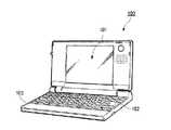
〔電子機器〕
以上のような構成の入力機能付液晶表示装置1は、例えば図5に示すようなモバイル型パーソナルコンピュータ100の表示部101として用いられる。このモバイル型パーソナルコンピュータ100は、表示部101と、キーボード102を有する本体部103とを備えている。〔Electronics〕
The liquid
以上のように、本実施形態における入力機能付液晶表示装置1によれば、対向基板12にシールド電極52を設けることで、対向基板12を大幅に厚肉化させずに複雑なシステムを用いることなく液晶層13の駆動時に発生するノイズの影響を抑制し、表示面への接触位置の検出精度が向上する。また、シールド電極52が偏光板として機能することで、液晶層13を透過してからシールド電極52に入射するまでの光の偏光状態の変化量を抑制し、コントラストが向上する。
また、画素電極21及び共通電極43とシールド電極52との距離が十分に確保されており、液晶層13の駆動時に発生するノイズの影響が縦電界方式の電極構造を用いる場合と比較して小さくなるので、シールド電極52によるノイズの遮断が有効に行われる。
そして、シールド電極52と検出電極15との間が十分に離間しているので、シールド電極52と検出電極15との間に容量成分が形成されない。
さらに、シールド電極52がAlなどの光反射性の導電材料で構成されており、シールド電極52で遮断される光を反射させるので、光の吸収による対向基板12の加熱を抑制できる。As described above, according to the liquid crystal display device with an
In addition, the distance between the
Since the
Furthermore, since the
[第2の実施形態]
次に、本発明における入力機能付液晶表示装置の第2の実施形態を、図面に基づいて説明する。ここで、図6は、サブ画素領域を示す断面図である。なお、本実施形態では、第1の実施形態とサブ画素領域の構成が異なるため、この点を中心に説明すると共に、上記実施形態で説明した構成要素には同一符号を付し、その説明を省略する。[Second Embodiment]
Next, a second embodiment of the liquid crystal display device with an input function according to the present invention will be described with reference to the drawings. Here, FIG. 6 is a cross-sectional view showing the sub-pixel region. In this embodiment, since the configuration of the sub-pixel region is different from that of the first embodiment, this point will be mainly described, and the same reference numerals are given to the components described in the above embodiment, and the description will be given. Omitted.
本実施形態における入力機能付液晶表示装置110では、図6に示すように、対向基板111に設けられたシールド電極112が遮光膜を兼ねている。
すなわち、対向基板111は、基板本体51と、基板本体51の内側の表面に順次積層されたシールド電極112、カラーフィルタ層54及び配向膜55とを備えている。
シールド電極112は、複屈折構造体112aと被覆部112bとを有している。
被覆部112bは、平面視でサブ画素領域の縁部であって液晶層13などを介してTFT素子22、データ線23及び走査線24と重なる領域に平面視でほぼ格子状に形成されており、サブ画素領域を縁取っている。In the liquid crystal display device with an
That is, the counter substrate 111 includes a
The
The covering
以上のように、本実施形態における入力機能付液晶表示装置110によっても、上述した実施形態と同様の作用、効果を奏するが、シールド電極112が遮光膜として機能することにより、部品点数の削減及び製造工程の簡略化が図れる。 As described above, the liquid crystal display device with an
なお、本発明は上記実施形態に限定されるものではなく、本発明の趣旨を逸脱しない範囲において種々の変更を加えることが可能である。
例えば、シールド電極を対向基板の端部に設けられた基板間導通部材を介して素子基板と導通させることによってシールド電極の電位を固定しているが、シールド電極の電位が固定されれば、他の方法を用いてもよい。
また、シールド電極をAlなどの光反射性を有する導電材料で構成しているが、例えばCr(クロム)などの光吸収性を有する導電材料で構成してもよい。これにより、シールド電極で遮断される光を吸収して反射による表示品質の劣化を防止できる。
そして、素子基板も、対向基板と同様に、液晶層側にワイヤグリッド構造を有する複数の複屈折構造体を設け、素子基板の外面に偏光板を配置しない構成としてもよい。In addition, this invention is not limited to the said embodiment, A various change can be added in the range which does not deviate from the meaning of this invention.
For example, the potential of the shield electrode is fixed by making the shield electrode conductive with the element substrate via the inter-substrate conductive member provided at the end of the counter substrate, but if the potential of the shield electrode is fixed, the other The method may be used.
The shield electrode is made of a light-reflective conductive material such as Al, but may be made of a light-absorbing conductive material such as Cr (chromium). Thereby, it is possible to absorb light blocked by the shield electrode and prevent display quality from being deteriorated due to reflection.
Further, similarly to the counter substrate, the element substrate may have a configuration in which a plurality of birefringent structures having a wire grid structure are provided on the liquid crystal layer side and no polarizing plate is disposed on the outer surface of the element substrate.
また、入力機能付液晶表示装置は、画素電極及び共通電極がFFS方式の電極構造を有しているが、IPS(In-Plane Switching)方式など、いわゆる横電界方式を用いた他の電極構造を採用してもよい。
そして、入力機能付液晶表示装置は、透過型の液晶表示装置となっているが、反射型や半透過反射型のような他の液晶表示装置の構成としてもよい。また、カラー液晶表示装置に限られない。In the liquid crystal display device with an input function, the pixel electrode and the common electrode have an FFS type electrode structure, but other electrode structures using a so-called lateral electric field type such as an IPS (In-Plane Switching) type are used. It may be adopted.
The liquid crystal display device with an input function is a transmissive liquid crystal display device, but may have a configuration of another liquid crystal display device such as a reflective type or a transflective type. Moreover, it is not restricted to a color liquid crystal display device.
また、入力機能付液晶表示装置を備える電子機器としては、モバイル型パーソナルコンピュータに限らず、携帯電話機やPDA(Personal Digital Assistant:携帯情報端末機)、パーソナルコンピュータ、ノート型パーソナルコンピュータ、ワークステーション、デジタルスチルカメラ、車載用モニタ、カーナビゲーション装置、ヘッドアップディスプレイ、デジタルビデオカメラ、テレビジョン受像機、ビューファインダ型あるいはモニタ直視型のビデオテープレコーダ、ページャ、電子手帳、電卓、電子ブックやプロジェクタ、ワードプロセッサ、テレビ電話機、POS端末、タッチパネルを備える機器などのような他の電子機器であってもよい。 In addition, the electronic device provided with the liquid crystal display device with an input function is not limited to a mobile personal computer, but a mobile phone, a PDA (Personal Digital Assistant), a personal computer, a notebook personal computer, a workstation, a digital Still camera, in-vehicle monitor, car navigation system, head-up display, digital video camera, television receiver, viewfinder type or monitor direct-view type video tape recorder, pager, electronic notebook, calculator, electronic book and projector, word processor, Other electronic devices such as a video phone, a POS terminal, a device including a touch panel may be used.
1,110 入力機能付液晶表示装置、11 素子基板(第1基板)、12,111 対向基板(第2基板)、13 液晶層、15 検出電極、17 誘電体膜、18 検出手段、21 画素電極(一方の電極)、43 共通電極(他方の電極)、52,112 シールド電極(シールド導体)、52a,112a 複屈折構造体、112b 被覆部1,110 liquid crystal display device with input function, 11 element substrate (first substrate), 12, 111 counter substrate (second substrate), 13 liquid crystal layer, 15 detection electrode, 17 dielectric film, 18 detection means, 21 pixel electrode (One electrode), 43 common electrode (the other electrode), 52, 112 shield electrode (shield conductor), 52a, 112a birefringent structure, 112b covering portion
Claims (4)
Translated fromJapanese該第1基板と前記液晶層を介して対向配置され、該液晶装置側に、電位が固定されると共に、ストライプ状に配置された複数の複屈折構造体を有するシールド導体を備える第2基板と、
前記第2基板の外面に積層して設けられた検出電極及び誘電体膜と、
該誘電体膜を介して前記検出電極との間に形成される静電容量の形成位置を検出する検出手段とを備え、
前記シールド導体が、該シールド導体に入射した光に対し、前記複屈折構造体の延在方向と略直交する偏光方向を有する偏光成分を透過させ、前記複屈折構造体の延在方向と略平行な偏光方向を有する偏光成分を遮断する入力機能付表示装置。A first substrate provided with a pair of electrodes for driving a liquid crystal layer;
A second substrateprovided with a shield conductor having a plurality of birefringent structures arranged in stripes and having a potential fixed to the first substrate and the liquid crystal layer, the potential being fixed on the liquid crystal device side; ,
A sensing electrode and a dielectric film provided on the outer surface of the second substrate;
Detecting means for detecting a formation position of a capacitance formed between the detection electrode and the detection electrode via the dielectric film;
The shield conductor transmits a polarization component having a polarization direction substantially orthogonal to the extending direction of the birefringent structure to the light incident on the shield conductor, and is substantially parallel to the extending direction of the birefringent structure. A display device withan input functionfor blocking a polarization component having a different polarization direction .
Priority Applications (5)
| Application Number | Priority Date | Filing Date | Title |
|---|---|---|---|
| JP2007019139AJP5008026B2 (en) | 2007-01-30 | 2007-01-30 | Display device with input function |
| US11/956,385US7633566B2 (en) | 2007-01-30 | 2007-12-14 | Input-capable display device |
| KR1020080006953AKR101456710B1 (en) | 2007-01-30 | 2008-01-23 | Input-capable display device |
| TW097102677ATWI442291B (en) | 2007-01-30 | 2008-01-24 | Input-capable display device |
| CN2008100032670ACN101236319B (en) | 2007-01-30 | 2008-01-28 | Display device with input function |
Applications Claiming Priority (1)
| Application Number | Priority Date | Filing Date | Title |
|---|---|---|---|
| JP2007019139AJP5008026B2 (en) | 2007-01-30 | 2007-01-30 | Display device with input function |
Publications (2)
| Publication Number | Publication Date |
|---|---|
| JP2008186714A JP2008186714A (en) | 2008-08-14 |
| JP5008026B2true JP5008026B2 (en) | 2012-08-22 |
Family
ID=39667516
Family Applications (1)
| Application Number | Title | Priority Date | Filing Date |
|---|---|---|---|
| JP2007019139AActiveJP5008026B2 (en) | 2007-01-30 | 2007-01-30 | Display device with input function |
Country Status (5)
| Country | Link |
|---|---|
| US (1) | US7633566B2 (en) |
| JP (1) | JP5008026B2 (en) |
| KR (1) | KR101456710B1 (en) |
| CN (1) | CN101236319B (en) |
| TW (1) | TWI442291B (en) |
Families Citing this family (59)
| Publication number | Priority date | Publication date | Assignee | Title |
|---|---|---|---|---|
| JP5051690B2 (en) | 2007-01-30 | 2012-10-17 | 株式会社ジャパンディスプレイウェスト | Display device with input function |
| JP4816668B2 (en) | 2008-03-28 | 2011-11-16 | ソニー株式会社 | Display device with touch sensor |
| JP4471019B2 (en)* | 2008-04-15 | 2010-06-02 | ソニー株式会社 | Illumination device and display device |
| JP5213581B2 (en)* | 2008-08-18 | 2013-06-19 | 株式会社ジャパンディスプレイウェスト | Display device |
| US8310609B2 (en)* | 2008-09-30 | 2012-11-13 | Sony Corporation | Liquid crystal device, electronic apparatus, and method of manufacturing liquid crystal device |
| JP5454872B2 (en)* | 2008-09-30 | 2014-03-26 | 株式会社ジャパンディスプレイ | Liquid crystal devices and electronic equipment |
| US20100117988A1 (en)* | 2008-11-12 | 2010-05-13 | Adrian Marc Simon Jacobs | Optical element and touch sensor |
| US20100208176A1 (en)* | 2009-02-17 | 2010-08-19 | Chi Mei Optoelectronics Corporation | Wide Viewing Angle Transflective Liquid Crystal Displays |
| JP5140018B2 (en) | 2009-02-24 | 2013-02-06 | 株式会社ジャパンディスプレイイースト | LCD with input function |
| JP2010211116A (en)* | 2009-03-12 | 2010-09-24 | Hitachi Displays Ltd | Display device incorporating touch panel |
| US8643624B2 (en)* | 2009-03-18 | 2014-02-04 | Synaptics Incorporated | Capacitive sensing using a segmented common voltage electrode of a display |
| TWI497157B (en)* | 2009-06-19 | 2015-08-21 | Tpk Touch Solutions Inc | Touch ips liquid crystal display |
| JP5297927B2 (en)* | 2009-07-22 | 2013-09-25 | 株式会社ジャパンディスプレイウェスト | LCD panel |
| JP5300640B2 (en) | 2009-07-27 | 2013-09-25 | 株式会社ジャパンディスプレイウェスト | Capacitance type input device and electro-optical device with input device |
| RU2012106129A (en)* | 2009-07-31 | 2013-09-10 | Шарп Кабусики Кайся | ELECTRODE SUBSTRATE, METHOD FOR MANUFACTURING ELECTRODE SUBSTRATE AND IMAGE DISPLAY DEVICE |
| JP5333969B2 (en)* | 2009-09-15 | 2013-11-06 | 株式会社ジャパンディスプレイ | Liquid crystal devices and electronic equipment |
| JP5255547B2 (en)* | 2009-10-13 | 2013-08-07 | アルプス電気株式会社 | Capacitive touchpad input device |
| JP5439114B2 (en)* | 2009-10-21 | 2014-03-12 | 株式会社ジャパンディスプレイ | Capacitance type input device and electro-optical device with input device |
| KR101695285B1 (en)* | 2009-12-22 | 2017-01-24 | 엘지디스플레이 주식회사 | Liquid Crystal Display Device and Method for Manufacturing the Same |
| CN102884496B (en)* | 2010-02-26 | 2017-06-30 | 辛纳普蒂克斯公司 | Modify demodulation to avoid interference |
| US9898121B2 (en) | 2010-04-30 | 2018-02-20 | Synaptics Incorporated | Integrated capacitive sensing and displaying |
| KR101319347B1 (en)* | 2010-06-10 | 2013-10-16 | 엘지디스플레이 주식회사 | Liquid Crystal Display Panel Associated with Touch Panel |
| JP5615647B2 (en)* | 2010-09-24 | 2014-10-29 | 株式会社ジャパンディスプレイ | Display device with touch detection function and electronic device |
| JP5682270B2 (en)* | 2010-12-06 | 2015-03-11 | 大日本印刷株式会社 | Measuring method using biosensor and biosensor |
| JP5925896B2 (en) | 2011-09-07 | 2016-05-25 | シナプティクス インコーポレイテッド | Capacitive detection during hidden update time |
| JP2013101420A (en)* | 2011-11-07 | 2013-05-23 | Japan Display West Co Ltd | Display device and electronic apparatus |
| KR101984161B1 (en)* | 2011-11-08 | 2019-05-31 | 삼성전자 주식회사 | Touch screen panel and portable device |
| US8970547B2 (en) | 2012-02-01 | 2015-03-03 | Synaptics Incorporated | Noise-adapting touch sensing window |
| WO2014000368A1 (en)* | 2012-06-29 | 2014-01-03 | 上海天马微电子有限公司 | Capacitive liquid crystal display touch panel |
| US10073568B2 (en) | 2012-08-15 | 2018-09-11 | Synaptics Incorporated | System and method for interference avoidance for a display device comprising an integrated sensing device |
| KR101968929B1 (en)* | 2012-09-11 | 2019-04-16 | 삼성디스플레이 주식회사 | Sensor substrate, method of manufacturing the same and sensing display panel having the same |
| US10073550B2 (en) | 2012-09-20 | 2018-09-11 | Synaptics Incorporated | Concurrent input sensing and display updating |
| KR102018740B1 (en)* | 2013-01-02 | 2019-09-06 | 삼성디스플레이 주식회사 | Display having touch sensing function |
| KR102141459B1 (en)* | 2013-03-22 | 2020-08-05 | 가부시키가이샤 한도오따이 에네루기 켄큐쇼 | Liquid crystal display device |
| KR20140118027A (en)* | 2013-03-28 | 2014-10-08 | 삼성디스플레이 주식회사 | Liquid crystal display device |
| CN103500044B (en)* | 2013-09-30 | 2015-08-12 | 京东方科技集团股份有限公司 | Touch display panel and touch display unit |
| US9442615B2 (en) | 2013-10-02 | 2016-09-13 | Synaptics Incorporated | Frequency shifting for simultaneous active matrix display update and in-cell capacitive touch |
| US9582099B2 (en) | 2014-03-31 | 2017-02-28 | Synaptics Incorporated | Serrated input sensing intervals |
| US9298309B2 (en) | 2014-04-29 | 2016-03-29 | Synaptics Incorporated | Source driver touch transmitter in parallel with display drive |
| US10175827B2 (en) | 2014-12-23 | 2019-01-08 | Synaptics Incorporated | Detecting an active pen using a capacitive sensing device |
| US9280233B1 (en)* | 2014-12-23 | 2016-03-08 | Synaptics Incorporated | Routing for touch sensor electrodes |
| US10394391B2 (en) | 2015-01-05 | 2019-08-27 | Synaptics Incorporated | System and method for reducing display artifacts |
| US10275070B2 (en) | 2015-01-05 | 2019-04-30 | Synaptics Incorporated | Time sharing of display and sensing data |
| WO2016140282A1 (en)* | 2015-03-03 | 2016-09-09 | シャープ株式会社 | Display device equipped with touch sensor |
| JP2016177280A (en)* | 2015-03-18 | 2016-10-06 | 株式会社半導体エネルギー研究所 | Display device, electronic device, and driving method of display device |
| TWI765634B (en)* | 2015-03-27 | 2022-05-21 | 日商半導體能源研究所股份有限公司 | Touch panel |
| CN104698700B (en) | 2015-04-01 | 2018-05-08 | 上海天马微电子有限公司 | Touch display panel and display device |
| CN104793803A (en)* | 2015-05-11 | 2015-07-22 | 京东方科技集团股份有限公司 | Touch control substrate and manufacturing method and touch control display device thereof |
| TWI562051B (en)* | 2015-09-04 | 2016-12-11 | Coretronic Corp | Touch projection screen and projection system |
| US10037112B2 (en) | 2015-09-30 | 2018-07-31 | Synaptics Incorporated | Sensing an active device'S transmission using timing interleaved with display updates |
| US10592022B2 (en) | 2015-12-29 | 2020-03-17 | Synaptics Incorporated | Display device with an integrated sensing device having multiple gate driver circuits |
| CN105718116A (en)* | 2016-02-01 | 2016-06-29 | 京东方科技集团股份有限公司 | Touch panel, manufacturing method thereof and touch display screen |
| JP6977074B2 (en)* | 2016-05-18 | 2021-12-08 | 株式会社ジャパンディスプレイ | Display device and sensor device |
| US20190348008A1 (en)* | 2016-08-22 | 2019-11-14 | Sharp Kabushiki Kaisha | Touch-panel-equipped display device |
| CN106501982A (en)* | 2016-12-13 | 2017-03-15 | 昆山龙腾光电有限公司 | Compound liquid crystal indicator |
| CN110945658A (en)* | 2017-05-09 | 2020-03-31 | Ka成像股份有限公司 | Apparatus for radiation detection in digital imaging system |
| CN110460705A (en)* | 2019-08-31 | 2019-11-15 | 深圳阜时科技有限公司 | Biological characteristic detection system and electronic equipment |
| CN112882272B (en) | 2021-03-01 | 2022-04-12 | 武汉华星光电技术有限公司 | Liquid crystal display device having a plurality of pixel electrodes |
| DE102023103809B3 (en)* | 2023-02-16 | 2024-08-01 | Novem Car Interior Design Gmbh | molded part |
Family Cites Families (7)
| Publication number | Priority date | Publication date | Assignee | Title |
|---|---|---|---|---|
| JP3573154B2 (en)* | 1996-03-14 | 2004-10-06 | セイコーエプソン株式会社 | Liquid crystal device and electronic equipment using the same |
| US6259490B1 (en)* | 1998-08-18 | 2001-07-10 | International Business Machines Corporation | Liquid crystal display device |
| JP3532146B2 (en)* | 2000-08-09 | 2004-05-31 | 住友ゴム工業株式会社 | Transparent electromagnetic wave shielding member and method of manufacturing the same |
| JP4507480B2 (en) | 2001-12-27 | 2010-07-21 | ソニー株式会社 | Display device |
| JP2006146895A (en) | 2004-10-22 | 2006-06-08 | Sharp Corp | Display device with touch sensor and driving method thereof |
| KR101374887B1 (en)* | 2006-05-16 | 2014-03-13 | 삼성디스플레이 주식회사 | Display panel |
| JP5051690B2 (en)* | 2007-01-30 | 2012-10-17 | 株式会社ジャパンディスプレイウェスト | Display device with input function |
- 2007
- 2007-01-30JPJP2007019139Apatent/JP5008026B2/enactiveActive
- 2007-12-14USUS11/956,385patent/US7633566B2/enactiveActive
- 2008
- 2008-01-23KRKR1020080006953Apatent/KR101456710B1/ennot_activeExpired - Fee Related
- 2008-01-24TWTW097102677Apatent/TWI442291B/enactive
- 2008-01-28CNCN2008100032670Apatent/CN101236319B/enactiveActive
Also Published As
| Publication number | Publication date |
|---|---|
| TWI442291B (en) | 2014-06-21 |
| US7633566B2 (en) | 2009-12-15 |
| KR101456710B1 (en) | 2014-10-31 |
| JP2008186714A (en) | 2008-08-14 |
| TW200839591A (en) | 2008-10-01 |
| CN101236319A (en) | 2008-08-06 |
| KR20080071490A (en) | 2008-08-04 |
| CN101236319B (en) | 2011-08-03 |
| US20080180584A1 (en) | 2008-07-31 |
Similar Documents
| Publication | Publication Date | Title |
|---|---|---|
| JP5008026B2 (en) | Display device with input function | |
| JP5051690B2 (en) | Display device with input function | |
| CN106605169B (en) | Liquid crystal display device and substrate for display device | |
| KR20090080487A (en) | Electro-optical devices, methods of manufacturing electro-optical devices, and electronic devices | |
| JP4924224B2 (en) | Photodetector built-in display device and electronic device | |
| JP5255876B2 (en) | Liquid crystal display device and electronic apparatus using the same | |
| US12169331B2 (en) | Display device with touch sensors and its wiring | |
| JP4905011B2 (en) | Liquid crystal device and electronic device | |
| JP4858082B2 (en) | Electro-optical device and electronic apparatus | |
| JP2008157997A (en) | Liquid crystal device and electronic device | |
| JP5397982B2 (en) | Liquid crystal display device and electronic device | |
| JP2008145572A (en) | Liquid crystal display | |
| JP4923947B2 (en) | Electro-optical device and electronic apparatus | |
| JP5009114B2 (en) | Liquid crystal display device and electronic device | |
| JP4905242B2 (en) | Liquid crystal device and electronic device | |
| JP2008209852A (en) | Liquid crystal device and electronic device | |
| JP2008275966A (en) | Liquid crystal display device and electronic equipment |
Legal Events
| Date | Code | Title | Description |
|---|---|---|---|
| A621 | Written request for application examination | Free format text:JAPANESE INTERMEDIATE CODE: A621 Effective date:20091111 | |
| A521 | Request for written amendment filed | Free format text:JAPANESE INTERMEDIATE CODE: A821 Effective date:20091112 | |
| A711 | Notification of change in applicant | Free format text:JAPANESE INTERMEDIATE CODE: A711 Effective date:20100526 | |
| RD02 | Notification of acceptance of power of attorney | Free format text:JAPANESE INTERMEDIATE CODE: A7422 Effective date:20100526 | |
| A977 | Report on retrieval | Free format text:JAPANESE INTERMEDIATE CODE: A971007 Effective date:20111013 | |
| A131 | Notification of reasons for refusal | Free format text:JAPANESE INTERMEDIATE CODE: A131 Effective date:20111018 | |
| A521 | Request for written amendment filed | Free format text:JAPANESE INTERMEDIATE CODE: A523 Effective date:20111216 | |
| TRDD | Decision of grant or rejection written | ||
| A711 | Notification of change in applicant | Free format text:JAPANESE INTERMEDIATE CODE: A711 Effective date:20120330 | |
| A01 | Written decision to grant a patent or to grant a registration (utility model) | Free format text:JAPANESE INTERMEDIATE CODE: A01 Effective date:20120403 | |
| A61 | First payment of annual fees (during grant procedure) | Free format text:JAPANESE INTERMEDIATE CODE: A61 Effective date:20120416 | |
| A01 | Written decision to grant a patent or to grant a registration (utility model) | Free format text:JAPANESE INTERMEDIATE CODE: A01 | |
| A61 | First payment of annual fees (during grant procedure) | Free format text:JAPANESE INTERMEDIATE CODE: A61 Effective date:20120523 | |
| R155 | Notification before disposition of declining of application | Free format text:JAPANESE INTERMEDIATE CODE: R155 | |
| R150 | Certificate of patent or registration of utility model | Free format text:JAPANESE INTERMEDIATE CODE: R150 Ref document number:5008026 Country of ref document:JP Free format text:JAPANESE INTERMEDIATE CODE: R150 | |
| FPAY | Renewal fee payment (event date is renewal date of database) | Free format text:PAYMENT UNTIL: 20150608 Year of fee payment:3 | |
| R250 | Receipt of annual fees | Free format text:JAPANESE INTERMEDIATE CODE: R250 | |
| R250 | Receipt of annual fees | Free format text:JAPANESE INTERMEDIATE CODE: R250 | |
| R250 | Receipt of annual fees | Free format text:JAPANESE INTERMEDIATE CODE: R250 | |
| R250 | Receipt of annual fees | Free format text:JAPANESE INTERMEDIATE CODE: R250 | |
| R250 | Receipt of annual fees | Free format text:JAPANESE INTERMEDIATE CODE: R250 | |
| S111 | Request for change of ownership or part of ownership | Free format text:JAPANESE INTERMEDIATE CODE: R313111 | |
| R350 | Written notification of registration of transfer | Free format text:JAPANESE INTERMEDIATE CODE: R350 | |
| R250 | Receipt of annual fees | Free format text:JAPANESE INTERMEDIATE CODE: R250 | |
| R250 | Receipt of annual fees | Free format text:JAPANESE INTERMEDIATE CODE: R250 | |
| R250 | Receipt of annual fees | Free format text:JAPANESE INTERMEDIATE CODE: R250 | |
| R250 | Receipt of annual fees | Free format text:JAPANESE INTERMEDIATE CODE: R250 | |
| R250 | Receipt of annual fees | Free format text:JAPANESE INTERMEDIATE CODE: R250 | |
| R250 | Receipt of annual fees | Free format text:JAPANESE INTERMEDIATE CODE: R250 | |
| S111 | Request for change of ownership or part of ownership | Free format text:JAPANESE INTERMEDIATE CODE: R313113 | |
| R350 | Written notification of registration of transfer | Free format text:JAPANESE INTERMEDIATE CODE: R350 |