JP5007860B2 - Vector processing equipment - Google Patents
Vector processing equipmentDownload PDFInfo
- Publication number
- JP5007860B2 JP5007860B2JP2007108256AJP2007108256AJP5007860B2JP 5007860 B2JP5007860 B2JP 5007860B2JP 2007108256 AJP2007108256 AJP 2007108256AJP 2007108256 AJP2007108256 AJP 2007108256AJP 5007860 B2JP5007860 B2JP 5007860B2
- Authority
- JP
- Japan
- Prior art keywords
- instruction
- issue
- stage
- flag
- order
- Prior art date
- Legal status (The legal status is an assumption and is not a legal conclusion. Google has not performed a legal analysis and makes no representation as to the accuracy of the status listed.)
- Expired - Fee Related
Links
- 238000001514detection methodMethods0.000claimsdescription14
- 238000003672processing methodMethods0.000claims4
- 230000002860competitive effectEffects0.000description1
- 238000010586diagramMethods0.000description1
- 230000000694effectsEffects0.000description1
Images


Landscapes
- Advance Control (AREA)
Description
Translated fromJapanese本発明は、ベクトル処理装置に関する。 The present invention relates to a vector processing device.
従来のベクトル処理装置を図3を参照して説明する。 A conventional vector processing apparatus will be described with reference to FIG.
図3において、901は命令デコードステージ1、902は命令デコーダ、903は命令デコードステージ2、904はリソース一致検出回路、905は命令発行ステージ0、906は命令発行ステージ1、907はビジーフラグ、908は発行チェック回路、909は発行ステージ0、1の発行指示、910は命令発行が命令発行ステージ0、1のどちらかを指示する命令指示フラグ、911は910の命令指示フラグでセレクトされた命令発行ステージ0、1の命令が格納される発行命令で構成される。901の命令デコードステージ1にセットされた命令は、902の命令デコーダで命令が使用するリソースのリクエストなどにデコードされ、903の命令デコードステージ2に格納される。発行ステージ905、906が空いていれば次クロックで発行ステージにセット可能だが空いていなければ空くまで待たされる。また、先行命令が905、906の発行ステージにある場合、903の命令デコードステージ2のリクエストと命令発行ステージ905、906の関係に一致があるかを904のリソース一致検出回路で検出する。一致が検出されると903の命令デコードステージ2に格納された命令リクエストは、一致が検出された先行命令が発行されるまで905の命令発行ステージ0、906の命令発行ステージ1のどちらかが空いていても命令をセットできず後続命令を待たせる課題があった。
従来のベクトル処理装置の命令追越し発行は、先行2命令の命令間でリソースの一致がある場合、後続命令は先行命令が発行されるまで発行ステージにセットできず、先行2命令間とリソースが一致しなくても実行することができず処理が止まってしまい性能低下になっていた。 In the instruction overtaking issue of the conventional vector processing apparatus, when there is a resource match between the instructions of the preceding two instructions, the succeeding instruction cannot be set in the issue stage until the preceding instruction is issued, and the resource between the preceding two instructions is one. Even if it did not do it, it could not be executed and the processing stopped and the performance was degraded.
本発明の目的は発行ステージに出来るだけ多くの命令をエントリさせることによりできるだけ多くの命令が追い越し発行できるベクトル処理装置を提供することにある。 An object of the present invention is to provide a vector processing apparatus in which as many instructions as possible can be overtaken by entering as many instructions as possible in an issue stage.
命令をグループに分けた複数の発行ステージ(図1の6、8)と、発行ステージ(図1の6、8)にセットされた命令とデコードステージ(図1の3)にセットされている後続命令とのリソースの関係(一致)を検出するリソース一致検出回路(図1の4)と、リソース一致検出回路(図1の4)の結果を格納する順序フラグ(図1の5、7)を有し、発行ステージ(図1の6、8)の順序フラグ(図1の5、7)が点灯していないことと、使用するリソースに対応するビジーフラグ(図1の9)が点灯していないことが満たされれば命令発行を可能にする手段。 Multiple issue stages (6, 8 in FIG. 1) that divide the instructions into groups, instructions set in the issue stage (6, 8 in FIG. 1), and successors set in the decode stage (3 in FIG. 1) A resource match detection circuit (4 in FIG. 1) for detecting a resource relationship (match) with an instruction and an order flag (5, 7 in FIG. 1) for storing the result of the resource match detection circuit (4 in FIG. 1). The order flag (5, 7 in FIG. 1) of the issue stage (6, 8 in FIG. 1) is not lit, and the busy flag (9 in FIG. 1) corresponding to the resource to be used is not lit A means of enabling issuance of instructions if this is satisfied.
本発明の効果は命令の実行順序を保障すべき場合のみ順序を保障し、その必要がない場合は複数命令の追い越し実行が可能となり性能の向上が期待できることである。 The effect of the present invention is that the order is guaranteed only when the instruction execution order is to be guaranteed, and when it is not necessary, the overtaking execution of a plurality of instructions is possible and the improvement in performance can be expected.
以下、図面を参照して本発明を実施するための最良の形態について詳細に説明する。 The best mode for carrying out the present invention will be described below in detail with reference to the drawings.
本発明は、ベクトル処理装置の命令発行制御部において、命令の実行順序を保障すべき場合のみ順序を保障し、その必要がない場合は複数命令の追い越し実行を可能とすることを特徴としている。 The present invention is characterized in that the instruction issuance control unit of the vector processing apparatus guarantees the order only when the instruction execution order should be guaranteed, and allows the overtaking execution of a plurality of instructions when it is not necessary.
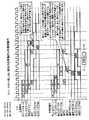
図1を参照すると、本発明の一実施形態としてのベクトル処理装置の発行制御部が示されている。図1において、1は命令デコードステージ1、2は命令デコーダ、3は命令デコードステージ2、4はリソース一致検出回路、5は6のA0発行ステージ(加算器系)にセットされた命令のA0発行ステージ(加算器系)順序フラグ、6はA0命令発行ステージ(加算器系)、7は8のM0発行ステージ(乗算器系)にセットされたM0発行ステージ(乗算器系)命令の順序フラグ、8はM0命令発行ステージ(乗算器系)、9はビジーフラグ、10はA0命令発行ステージの命令発行チェック回路、11はM0命令発行ステージの命令発行チェック回路、12はA0発行ステージの発行指示、13はM0発行ステージの発行指示で構成される。順序フラグとは、自命令が発行ステージにセットされる時点で、他の発行ステージに自命令より順序が先である命令が存在することを示すフラグである。順序フラグには他の発行ステージに対応したフラグがそれぞれあり、順序フラグに対応した発行ステージの命令が発行された時点でリセットされ、順序フラグが全てリセットになった時点で自命令のリクエストに対応したビジーフラグをチェックして発行可能になる。発行ステージにセットされている未発行の先行命令と後続命令間の発行順序はリソース一致がある場合は順序フラグで発行管理し、発行済みの命令はビジーフラグで後続命令を発行管理する。以下説明を容易にする為、順序フラグと発行ステージの組み合わせを5、6と7、8の2個で説明する。1の命令デコードステージ1にセットされた命令は、2の命令デコーダで命令が使用するリソースのリクエストにデコードされ、3の命令デコードステージ2に格納される。発行ステージ6、8が空いていれば次クロックで発行ステージにセット可能だが空いていなければ空くまで待たされる。先行命令が6、8の発行ステージにある場合、3の命令デコードステージ2のリクエストと命令発行ステージ6、8のリクエストの関係に一致があるかを4のリソース一致検出回路で検出する。検出結果は、命令発行ステージ6が空けば5のA0発行ステージ順序フラグにセットされ、命令発行ステージ8が空けば7のM0発行ステージ順序フラグにセットされる。3の命令デコードステージ2に格納された命令リクエストは、命令発行ステージ6が空けば命令発行ステージ6にセットされ、命令発行ステージ8が空けば命令発行ステージ8にセットされる。命令発行ステージ6、8が空いている場合は命令順や命令種別の規則に従ってセットされる。10のA0発行チェック回路は、6のA0命令発行ステージの命令リクエストに対応するリソースが空いているかを9のビジーフラグでチェックするのと、先行命令に順序を保障しなければならない命令があるかを5のA0順序フラグでチェックする。両チェックがOKになると12の命令発行指示が点灯し、6のA0命令発行ステージの命令リクエストに対応した9のビジーフラグがセットされ、7のM0発行ステージ順序フラグ内のA0命令発行ステージに対応した順序フラグがリセットされる。同様に11のM0発行チェック回路は、8のM0命令発行ステージの命令リクエストに対応するリソースが空いているかを9のビジーフラグでチェックするのと、先行命令に順序を保障しなければならない命令があるかを7のM0順序フラグでチェックする。両チェックがOKになると13の命令発行指示が点灯し、8のM0命令発行ステージの命令リクエストに対応した9のビジーフラグがセットされ、5のA0発行ステージ順序フラグ内のM0命令発行ステージに対応した順序フラグがリセットされる。上記の説明で発行ステージにセットされた時点での複数の発行ステージにセットされている先行命令との関係を順序フラグで示すことにより順序が保障され、順序フラグが全てリセットになった時点で発行が可能になり後続の命令でも先行命令とのリソースの一致がなければ先行命令を複数追い越しての発行が可能になる。 Referring to FIG. 1, an issue control unit of a vector processing apparatus as an embodiment of the present invention is shown. In FIG. 1, 1 is an
次に図1のベクトル処理装置の下記命令列の動作を図2に示すタイムチャートを使用して説明する。
(1) V2 <− V0 + V1
(2) V3 <− V6 + V7
(3) V0 <− V4 * V5
図1、2において命令間でリソースの一致がないケースを従来技術と比較して説明する。Next, the operation of the following instruction sequence of the vector processing apparatus of FIG. 1 will be described using the time chart shown in FIG.
(1) V2 <-V0 + V1
(2) V3 <-V6 + V7
(3) V0 <-V4 * V5
A case where there is no resource match between instructions in FIGS. 1 and 2 will be described in comparison with the prior art.
INから上記の命令順で図1−1の命令デコードステージ1に(1)がセットされる。次クロックで(1)の命令は図1−2の命令デコーダで命令が使用するリソースのリクエスト、READリクエストV0、V1、WriteリクエストV2、使用演算器A(加算器系)にデコードされ図1−3の命令デコードステージ2にセットされると同時に(2)の命令が図1−1の命令デコードステージ1にセットされる。次に図1−3の命令デコードステージ2にセットされた(1)の命令は加算器系命令なので図1−6のA0発行ステージにセットされるが図1−5のA0発行ステージ順序フラグには先行命令がない為何もセットされない。図1−1の命令デコードステージ1の(2)の命令は、図1−2の命令デコーダで命令が使用するリソースのリクエスト、READリクエストV6、V7、WriteリクエストV3、使用演算器A(加算器系)にデコードされ図1−3の命令デコードステージ2にセットされると同時に(3)の命令が図1−1の命令デコードステージ1にセットされる。図1−6のA0発行ステージにセットされた(1)の命令はREADリクエストV0、V1、WriteリクエストV2、使用演算器A(加算器系)に対応する図1−9のビジーフラグが点灯してないことと図1−5のA0発行ステージ順序フラグが全てリセットされていることをチェックして図1−12の命令発行指示を点灯する。次クロックで図1−12の命令発行指示によりの命令のREADリクエストV0、V1、WriteリクエストV2、使用演算器A(加算器系)に対応する図1−9のビジーフラグをセットすると同時に図1−3の命令デコードステージ2にセットされている(2)の命令が図1−6のA0発行ステージにセットされる。この時図1−5のA0発行ステージ順序フラグは再セットされる。図1−1の命令デコードステージ1の(3)命令は図1−2の命令デコーダで命令が使用するリソースのリクエスト、READリクエストV4、V5、WriteリクエストV0、使用演算器M(乗算器系)にデコードされ図1−3の命令デコードステージ2にセットされる。(1)命令の発行で使用演算器Aのビジーを示す図2のビジーフラグAがセットされ図1−6のA0発行ステージの後続(2)命令はビジーフラグAがリセットされるまで発行は抑止される。ここで従来動作では図1−6のA0発行ステージ、図1−8のM0発行ステージに値する発行ステージは1個のみだった為、図2の従来動作参照、先行命令(2)が発行されるまで図1−3の命令デコードステージ2の(3)命令は発行ステージが空くまで待たされることになる。図2の本発明動作では、順序フラグを発行ステージに設置することにより、図1−6のA0発行ステージ、図1−8のM0発行ステージの発行ステージを複数増設することが可能になり、図1−3の(3)命令は待つことなく空いている図1−8のM0発行ステージにセット可能になり、リソースの一致がない為即座に発行される。 (1) is set in the instruction decode stage 1 in FIG. In the next clock, the instruction (1) is decoded by the instruction decoder shown in FIG. 1-2 into a request for resources used by the instruction, a READ request V0, V1, a Write request V2, and a computing unit A (adder system). At the same time, the instruction (2) is set in the instruction decode stage 1 in FIG. Next, since the instruction (1) set in the
引用文献1については段落0028〜0029で競合検査において処理中のリソースと後続のリソースが一致した時に命令の発行を抑止するという記載があるが、本発明では修理中(演算実行)の命令と後続未発行の命令はBUSY FLAGで抑止する点で相違する。Subsequent the references 1 and resource being processed in a competitive test in paragraph 0028 to 0,029 but subsequent resourceis described called suppressing the issuance of instructions when matched, being repaired in the present invention and instructions (execution) An unissued instruction is different in that it is suppressed by BUSY FLAG.
引用文献2については第0012〜0014に記載の実行制御手段に命令順でセットされ、命令セット順で実行され、ビジー状態をチェックする事なく演算の終了をみて後続命令を発行すると言う動作よりも、本発明のBUSY FLAGで後続命令の発行タイミングを調整したほうが命令発行の前倒しができる。 For the cited
本発明によれば、複数のフラグを用いて複数命令の追い越し実行を可能とする命令発行制御部を備える。 According to the present invention, an instruction issuance control unit that enables overtaking execution of a plurality of instructions using a plurality of flags is provided.
命令発行とパイプライン処理中の取り方で変わってくるが、本発明の命令発行とは演算の実行を示し、命令発行と同時にリソースに対するBUSY FLAGをSETしBUSY FLAG点灯中は後続命令の発行(演算実行)を抑止する。BUSY FLAGには演算ラテンシ(レイテンシ)に合わせて数種類用意しリソースの使用に隙間ができない様にしている。
Depending on how the instruction is issued and how it is taken during pipeline processing, the instruction issuance according to the present invention indicates the execution of an operation. execution)to suppress. Several types of BUSY FLAG are prepared in accordance with the operation latency (latency) so that there is no gap in the use of resources.
本発明の順序FLAGとは発行(演算実行)する前の順序を示す手段でDATAを壊さない様に順序を決める。命令を発行するステージを発行ステージと呼んでいるが、発行ステージにある命令は未発行であり、後続の命令が発行ステージにSETされる時には自分よりも前に発行ステージにSETされた命令との関係を知る必要がありリソースの一致が検出された場合は相手に対応する順序FLAGを発行ステージSETと同時にSETする。SETされた順序FLAGは順序FLAGに対応する発行ステージの命令が発行(演算実行)と同時にRESETされる。後続命令は順序FLAGが全てRESETされて発行の権利を得ることができる。次に発行の権利を得た発行ステージの命令は自分のリソースに対応するBUSY FLAGをチェックする。対応するBUSY FLAGが全てRESETされたことをチェックして発行(演算実行)する。 The order FLAG of the present invention is a means for indicating the order before issuance (calculation execution) and determines the order so as not to break DATA. The stage that issues an instruction is called the issue stage, but the instruction in the issue stage has not been issued, and when a subsequent instruction is set in the issue stage, the instruction set in the issue stage before itself is If it is necessary to know the relationship and a resource match is detected, the order FLAG corresponding to the partner is set simultaneously with the issue stage SET. The set order FLAG is reset simultaneously with the issuance (operation execution) of the instruction at the issue stage corresponding to the order FLAG. Subsequent instructions can be issued with all sequence FLAGs being reset. Next, the instruction of the issue stage that has obtained the issue right checks the BUSY FLAG corresponding to its own resource. Check that all corresponding BUSY FLAGs have been reset and issue (calculate).
発行ステージをハードウェア量が許す限り増やせば後続命令が先行命令を追い越すケースを増やすことができリソースを有効に使用できる。また、デコードステージに滞留するTOTAL時間を短くできる。 If the issue stage is increased as much as the hardware amount permits, the number of cases where the subsequent instruction overtakes the preceding instruction can be increased, and resources can be used effectively. Further, the TOTAL time staying in the decode stage can be shortened.
1 デコードステージ1
2 命令デコーダ
3 命令デコードステージ2
4 リソース一致検出回路
5 A0発行ステージ(加算器系)にセットされた命令のA0発行ステージ(加算器系)順序フラグ
6 A0命令発行ステージ(加算器系)
7 8のM0発行ステージ(乗算器系)にセットされたM0発行ステージ(乗算器系)命令の順序フラグ
8 M0命令発行ステージ(乗算器系)
9 ビジーフラグ
10 A0命令発行ステージの命令発行チェック回路
11 M0命令発行ステージの命令発行チェック回路
12 A0発行ステージの発行指示
13 M0発行ステージの発行指示1 Decode stage 1
2 Instruction decoder 3
4 Resource
7 M0 issue stage (multiplier system) instruction sequence flag set in 8 M0 issue stages (multiplier system) 8 M0 instruction issue stage (multiplier system)
9
Claims (4)
Translated fromJapanese複数の演算器リソースと、
命令の実行順序を保障すべき場合のみ順序を保障し、その必要がない場合は複数命令の追い越し実行を可能とする命令発行制御部と、
を具備するベクトル処理装置であって、
前記命令発行制御部は、
リソース一致検出回路(4)と、
前記複数の演算器リソースのそれぞれに対応する複数の発行ステージ(6、8)と、
該複数の発行ステージのそれぞれに対応する、複数の順序フラグ(5、7)及び複数のビジーフラグ(9のそれぞれのフラグ)を備え、
前記順序フラグは、他の演算器リソースに対応したフラグを有し、自命令が発行ステージにセットされる時点で、他の発行ステージに自命令より先に発行すべき命令が存在するか否かを示すものであり、
前記ビジーフラグは、対応する演算器リソースが空いているのか否かを示すものであり、
前記デコードステージにセットされた命令リクエストを、該命令リクエストが使用する演算器リソースで振り分けて前記複数の発行ステージにセットし、
前記リソース一致検出回路で、前記複数の発行ステージにセットした命令リクエストと前記デコードステージにセットされている後続命令の命令リクエストとのベクタレジスタの関係(一致)を検出してその検出結果を順序フラグに格納し、
前記複数の発行ステージの各発行ステージにおいて、
前記順序フラグが点灯していないことと、前記ビジーフラグが点灯していないことが満たされれば、当該発行ステージにセットした命令リクエストを発行することを特徴とするベクトル処理装置。A decoder (2) for decoding an instruction and setting an instruction request as a decoding result to the decode stage (3);
Multiple calculator resources,
An instruction issuance control unit that guarantees the order only when the instruction execution order should be guaranteed, and enables the overtaking execution of multiple instructions when it is not necessary;
A vector processing device comprising:
The command issue control unit
A resource match detection circuit (4);
A plurality of issue stages (6, 8) corresponding to each of the plurality of computing unit resources;
A plurality of order flags (5, 7) and a plurality of busy flags (each of 9 flags) corresponding to each of the plurality of issue stages,
The order flag has a flag corresponding to another arithmetic unit resource, and whether or not there is an instruction to be issued prior to the self instruction at the other issue stage when the self instruction is set in the issue stage. Indicates
The busy flag indicates whether or not the corresponding computing unit resource is free,
The instruction request set in the decode stage is distributed to the computing resources used by the instruction request and set in the plurality of issue stages,
The resource match detection circuit detects a relationship (match) of vector registers between an instruction request set in the plurality of issue stages and an instruction request of a subsequent instruction set in the decode stage, and the detection result is an order flag. Stored in
In each issue stage of the plurality of issue stages,
Andsaid sequence flag is not lit, if satisfiedthat the busy flag is noton, the vector processing apparatus andissues an instruction request set at the issue stage.
ある1つの命令発行ステージにセットされた命令リクエストが発行可能になると、その命令リクエストが使用する演算器リソースに対応する前記ビジーフラグをセットし、他の命令発行ステージの前記順序フラグの前記使用する演算器リソースに対応するフラグをリセットする手段を更に備えることを特徴とするベクトル処理装置。The vector processing device according to claim 1,
Whenthe set command requeststo asingle instruction issue stage becomes possible to issue, to setthe busy flag which corresponds to theoperation unit resource by the instruction requestis used,calculation of the use ofthe sequence flagsof other instruction issue stageThe vector processing apparatus further comprising means for resettinga flag corresponding to the container resource .
複数の演算器リソースと、
命令の実行順序を保障すべき場合のみ順序を保障し、その必要がない場合は複数命令の追い越し実行を可能とする命令発行制御部と、
を具備し、
前記命令発行制御部は、
リソース一致検出回路(4)と、
前記複数の演算器リソースのそれぞれに対応する複数の発行ステージ(6、8)と、
該複数の発行ステージのそれぞれに対応する、複数の順序フラグ(5、7)及び複数のビジーフラグ(9のそれぞれのフラグ)を備えるベクトル処理装置におけるベクトル処理方法であって、
前記順序フラグは、他の演算器リソースに対応したフラグを有し、自命令が発行ステージにセットされる時点で、他の発行ステージに自命令より先に発行すべき命令が存在するか否かを示すものであり、
前記ビジーフラグは、対応する演算器リソースが空いているのか否かを示すものであり、
前記デコードステージにセットされた命令リクエストを、該命令リクエストが使用する演算器リソースで振り分けて前記複数の発行ステージにセットし、
前記リソース一致検出回路で、前記複数の発行ステージにセットした命令リクエストと前記デコードステージにセットされている後続命令の命令リクエストとのベクタレジスタの関係(一致)を検出してその検出結果を順序フラグに格納し、
前記複数の発行ステージの各発行ステージにおいて、
前記順序フラグが点灯していないことと、前記ビジーフラグが点灯していないことが満たされれば、該発行ステージにセットした命令リクエストを発行することを特徴とするベクトル処理方法。A decoder (2) for decoding an instruction and setting an instruction request as a decoding result to the decode stage (3);
Multiple calculator resources,
Aninstruction issuance control unit that guarantees the order only when the instruction execution order should be guaranteed, and enables the overtaking execution of multiple instructions when it is not necessary;
Comprising
The command issue control unit
A resource match detection circuit (4);
A plurality of issue stages (6, 8) corresponding to each of the plurality of computing unit resources;
A vector processing methodin a vector processingdevice comprising a plurality of order flags (5, 7) and a plurality of busy flags (each of 9 flags) corresponding to each of the plurality of issue stages ,
The order flag has a flag corresponding to another arithmetic unit resource, and whether or not there is an instruction to be issued prior to the self instruction at the other issue stage when the self instruction is set in the issue stage. Indicates
The busy flag indicates whether or not the corresponding computing unit resource is free,
The instruction request set in the decode stage is distributed to the computing resources used by the instruction request and set in the plurality of issue stages,
The resource match detection circuit detects a relationship (match) of vector registers between an instruction request set in the plurality of issue stages and an instruction request of a subsequent instruction set in the decode stage, and the detection result is an order flag. Stored in
In each issue stage of the plurality of issue stages,
Andsaid sequence flag is not lit, if satisfiedthat the busy flag is noton, vector processingmethod characterized byissuing instructions request set at the issue stage.
ある1つの命令発行ステージにセットされた命令リクエストが発行可能になると、その命令リクエストが使用する演算器リソースに対応する前記ビジーフラグをセットし、他の命令発行ステージの前記順序フラグの前記使用する演算器リソースに対応するフラグをリセットする手順を更に有することを特徴とするベクトル処理方法。The vector processing method according to claim 3, wherein
Whenthe set command requeststo asingle instruction issue stage becomes possible to issue, to setthe busy flag which correspondsto the operation unit resource by the instruction requestis used,calculation of the use ofthe sequence flagsof other instruction issue stage A vector processing method further comprising a step of resettinga flag corresponding to a container resource .
Priority Applications (1)
| Application Number | Priority Date | Filing Date | Title |
|---|---|---|---|
| JP2007108256AJP5007860B2 (en) | 2007-04-17 | 2007-04-17 | Vector processing equipment |
Applications Claiming Priority (1)
| Application Number | Priority Date | Filing Date | Title |
|---|---|---|---|
| JP2007108256AJP5007860B2 (en) | 2007-04-17 | 2007-04-17 | Vector processing equipment |
Publications (2)
| Publication Number | Publication Date |
|---|---|
| JP2008269067A JP2008269067A (en) | 2008-11-06 |
| JP5007860B2true JP5007860B2 (en) | 2012-08-22 |
Family
ID=40048518
Family Applications (1)
| Application Number | Title | Priority Date | Filing Date |
|---|---|---|---|
| JP2007108256AExpired - Fee RelatedJP5007860B2 (en) | 2007-04-17 | 2007-04-17 | Vector processing equipment |
Country Status (1)
| Country | Link |
|---|---|
| JP (1) | JP5007860B2 (en) |
Families Citing this family (2)
| Publication number | Priority date | Publication date | Assignee | Title |
|---|---|---|---|---|
| JP4985452B2 (en)* | 2008-02-14 | 2012-07-25 | エヌイーシーコンピュータテクノ株式会社 | Vector processing equipment |
| JP5871298B2 (en)* | 2009-09-10 | 2016-03-01 | Necプラットフォームズ株式会社 | Information processing apparatus, information processing method, and information processing program |
Family Cites Families (4)
| Publication number | Priority date | Publication date | Assignee | Title |
|---|---|---|---|---|
| JPS5729153A (en)* | 1980-07-29 | 1982-02-17 | Fujitsu Ltd | Control system for instruction processing order |
| JPS6116335A (en)* | 1984-07-02 | 1986-01-24 | Nec Corp | Information processor |
| JPH03263265A (en)* | 1990-03-14 | 1991-11-22 | Koufu Nippon Denki Kk | Vector processor |
| EP0651321B1 (en)* | 1993-10-29 | 2001-11-14 | Advanced Micro Devices, Inc. | Superscalar microprocessors |
- 2007
- 2007-04-17JPJP2007108256Apatent/JP5007860B2/ennot_activeExpired - Fee Related
Also Published As
| Publication number | Publication date |
|---|---|
| JP2008269067A (en) | 2008-11-06 |
Similar Documents
| Publication | Publication Date | Title |
|---|---|---|
| KR101746018B1 (en) | Method and apparatus for efficient scheduling for asymmetrical execution units | |
| US9760411B2 (en) | Switching a locking mode of an object in a multi-thread program | |
| US8555256B2 (en) | Pass-by breakpoint setting and debugging method and device | |
| US20120222035A1 (en) | Priority Inheritance in Multithreaded Systems | |
| US20100050184A1 (en) | Multitasking processor and task switching method thereof | |
| KR20150129316A (en) | Eliminating redundant synchronization barriers in instruction processing circuits, and related processor systems, methods, and computer-readable media | |
| US11182318B2 (en) | Processor and interrupt controller | |
| KR100983135B1 (en) | Processor and method for grouping and executing dependency instructions of packets | |
| JP2005235135A (en) | Vector processor and passing control circuit | |
| US8601242B2 (en) | Adaptive optimized compare-exchange operation | |
| CN114168202A (en) | Instruction scheduling method, instruction scheduling device, processor and storage medium | |
| JP4985452B2 (en) | Vector processing equipment | |
| JP5007860B2 (en) | Vector processing equipment | |
| CN108139938A (en) | Apparatus, method and computer program for utilizing secondary threads to assist main thread in performing application tasks | |
| JP5195408B2 (en) | Multi-core system | |
| US20100211759A1 (en) | Apparatus and method for generating vliw, and processor and method for processing vliw | |
| US11436013B2 (en) | Method and system for detection of thread stall | |
| JP2008269114A (en) | Multi-thread processor and inter-thread synchronization operating method used for the same | |
| EP3591518B1 (en) | Processor and instruction scheduling method | |
| US20140201505A1 (en) | Prediction-based thread selection in a multithreading processor | |
| US9164767B2 (en) | Instruction control circuit, processor, and instruction control method | |
| US9378023B2 (en) | Cross-pipe serialization for multi-pipeline processor | |
| US20160020897A1 (en) | Using thresholds to gate timing packet generation in a tracing system | |
| US10671398B2 (en) | Low-overhead, low-latency operand dependency tracking for instructions operating on register pairs in a processor core | |
| US8516231B2 (en) | Interrupt handling apparatus and method for equal-model processor and processor including the interrupt handling apparatus |
Legal Events
| Date | Code | Title | Description |
|---|---|---|---|
| A621 | Written request for application examination | Free format text:JAPANESE INTERMEDIATE CODE: A621 Effective date:20080917 | |
| RD03 | Notification of appointment of power of attorney | Free format text:JAPANESE INTERMEDIATE CODE: A7423 Effective date:20100902 | |
| RD04 | Notification of resignation of power of attorney | Free format text:JAPANESE INTERMEDIATE CODE: A7424 Effective date:20100902 | |
| A977 | Report on retrieval | Free format text:JAPANESE INTERMEDIATE CODE: A971007 Effective date:20101210 | |
| A131 | Notification of reasons for refusal | Free format text:JAPANESE INTERMEDIATE CODE: A131 Effective date:20101215 | |
| A521 | Request for written amendment filed | Free format text:JAPANESE INTERMEDIATE CODE: A523 Effective date:20110119 | |
| A131 | Notification of reasons for refusal | Free format text:JAPANESE INTERMEDIATE CODE: A131 Effective date:20111020 | |
| A521 | Request for written amendment filed | Free format text:JAPANESE INTERMEDIATE CODE: A523 Effective date:20111216 | |
| TRDD | Decision of grant or rejection written | ||
| A01 | Written decision to grant a patent or to grant a registration (utility model) | Free format text:JAPANESE INTERMEDIATE CODE: A01 Effective date:20120507 | |
| A01 | Written decision to grant a patent or to grant a registration (utility model) | Free format text:JAPANESE INTERMEDIATE CODE: A01 | |
| A61 | First payment of annual fees (during grant procedure) | Free format text:JAPANESE INTERMEDIATE CODE: A61 Effective date:20120516 | |
| R150 | Certificate of patent or registration of utility model | Ref document number:5007860 Country of ref document:JP Free format text:JAPANESE INTERMEDIATE CODE: R150 Free format text:JAPANESE INTERMEDIATE CODE: R150 | |
| FPAY | Renewal fee payment (event date is renewal date of database) | Free format text:PAYMENT UNTIL: 20150608 Year of fee payment:3 | |
| S111 | Request for change of ownership or part of ownership | Free format text:JAPANESE INTERMEDIATE CODE: R313111 | |
| R350 | Written notification of registration of transfer | Free format text:JAPANESE INTERMEDIATE CODE: R350 | |
| LAPS | Cancellation because of no payment of annual fees |