JP5006102B2 - Light emitting device and manufacturing method thereof - Google Patents
Light emitting device and manufacturing method thereofDownload PDFInfo
- Publication number
- JP5006102B2 JP5006102B2JP2007132552AJP2007132552AJP5006102B2JP 5006102 B2JP5006102 B2JP 5006102B2JP 2007132552 AJP2007132552 AJP 2007132552AJP 2007132552 AJP2007132552 AJP 2007132552AJP 5006102 B2JP5006102 B2JP 5006102B2
- Authority
- JP
- Japan
- Prior art keywords
- phosphor
- transparent resin
- light emitting
- emitting device
- substrate
- Prior art date
- Legal status (The legal status is an assumption and is not a legal conclusion. Google has not performed a legal analysis and makes no representation as to the accuracy of the status listed.)
- Expired - Fee Related
Links
Images


Classifications
- H—ELECTRICITY
- H10—SEMICONDUCTOR DEVICES; ELECTRIC SOLID-STATE DEVICES NOT OTHERWISE PROVIDED FOR
- H10H—INORGANIC LIGHT-EMITTING SEMICONDUCTOR DEVICES HAVING POTENTIAL BARRIERS
- H10H20/00—Individual inorganic light-emitting semiconductor devices having potential barriers, e.g. light-emitting diodes [LED]
- H10H20/80—Constructional details
- H10H20/85—Packages
- H10H20/852—Encapsulations
- H10H20/853—Encapsulations characterised by their shape
- H—ELECTRICITY
- H10—SEMICONDUCTOR DEVICES; ELECTRIC SOLID-STATE DEVICES NOT OTHERWISE PROVIDED FOR
- H10H—INORGANIC LIGHT-EMITTING SEMICONDUCTOR DEVICES HAVING POTENTIAL BARRIERS
- H10H20/00—Individual inorganic light-emitting semiconductor devices having potential barriers, e.g. light-emitting diodes [LED]
- H10H20/80—Constructional details
- H10H20/84—Coatings, e.g. passivation layers or antireflective coatings
- H10H20/841—Reflective coatings, e.g. dielectric Bragg reflectors
- H—ELECTRICITY
- H10—SEMICONDUCTOR DEVICES; ELECTRIC SOLID-STATE DEVICES NOT OTHERWISE PROVIDED FOR
- H10H—INORGANIC LIGHT-EMITTING SEMICONDUCTOR DEVICES HAVING POTENTIAL BARRIERS
- H10H20/00—Individual inorganic light-emitting semiconductor devices having potential barriers, e.g. light-emitting diodes [LED]
- H10H20/80—Constructional details
- H10H20/85—Packages
- H10H20/851—Wavelength conversion means
- H10H20/8515—Wavelength conversion means not being in contact with the bodies
- H—ELECTRICITY
- H01—ELECTRIC ELEMENTS
- H01L—SEMICONDUCTOR DEVICES NOT COVERED BY CLASS H10
- H01L2224/00—Indexing scheme for arrangements for connecting or disconnecting semiconductor or solid-state bodies and methods related thereto as covered by H01L24/00
- H01L2224/01—Means for bonding being attached to, or being formed on, the surface to be connected, e.g. chip-to-package, die-attach, "first-level" interconnects; Manufacturing methods related thereto
- H01L2224/42—Wire connectors; Manufacturing methods related thereto
- H01L2224/44—Structure, shape, material or disposition of the wire connectors prior to the connecting process
- H01L2224/45—Structure, shape, material or disposition of the wire connectors prior to the connecting process of an individual wire connector
- H01L2224/45001—Core members of the connector
- H01L2224/45099—Material
- H01L2224/451—Material with a principal constituent of the material being a metal or a metalloid, e.g. boron (B), silicon (Si), germanium (Ge), arsenic (As), antimony (Sb), tellurium (Te) and polonium (Po), and alloys thereof
- H01L2224/45138—Material with a principal constituent of the material being a metal or a metalloid, e.g. boron (B), silicon (Si), germanium (Ge), arsenic (As), antimony (Sb), tellurium (Te) and polonium (Po), and alloys thereof the principal constituent melting at a temperature of greater than or equal to 950°C and less than 1550°C
- H01L2224/45144—Gold (Au) as principal constituent
- H—ELECTRICITY
- H01—ELECTRIC ELEMENTS
- H01L—SEMICONDUCTOR DEVICES NOT COVERED BY CLASS H10
- H01L2224/00—Indexing scheme for arrangements for connecting or disconnecting semiconductor or solid-state bodies and methods related thereto as covered by H01L24/00
- H01L2224/01—Means for bonding being attached to, or being formed on, the surface to be connected, e.g. chip-to-package, die-attach, "first-level" interconnects; Manufacturing methods related thereto
- H01L2224/42—Wire connectors; Manufacturing methods related thereto
- H01L2224/47—Structure, shape, material or disposition of the wire connectors after the connecting process
- H01L2224/48—Structure, shape, material or disposition of the wire connectors after the connecting process of an individual wire connector
- H01L2224/4805—Shape
- H01L2224/4809—Loop shape
- H01L2224/48091—Arched
- H—ELECTRICITY
- H10—SEMICONDUCTOR DEVICES; ELECTRIC SOLID-STATE DEVICES NOT OTHERWISE PROVIDED FOR
- H10H—INORGANIC LIGHT-EMITTING SEMICONDUCTOR DEVICES HAVING POTENTIAL BARRIERS
- H10H20/00—Individual inorganic light-emitting semiconductor devices having potential barriers, e.g. light-emitting diodes [LED]
- H10H20/01—Manufacture or treatment
- H10H20/036—Manufacture or treatment of packages
- H10H20/0361—Manufacture or treatment of packages of wavelength conversion means
Landscapes
- Led Device Packages (AREA)
Description
Translated fromJapanese本発明は、基板の上に発光ダイオード(LED)チップを搭載して、その外側に蛍光体を含有する透明樹脂を配置した発光装置と、かかる発光装置の製造方法に関する。 The present invention relates to a light-emitting device in which a light-emitting diode (LED) chip is mounted on a substrate and a transparent resin containing a phosphor is disposed on the outside thereof, and a method for manufacturing such a light-emitting device.
低波長の励起光を発するLEDチップと、波長変換性能を持つ蛍光体粒子の組み合わせによる白色LED発光装置は、従来、反射板つき基板上にLEDチップを設置し、その上に黄色の蛍光体粒子を分散した透明樹脂層を塗布することによって形成されるものが知られている(特許文献1参照)。しかしこの方法では、一様に蛍光体が分布するため、LEDチップから蛍光体層を通過する光路が長いほど発光が黄色を帯びてしまい、結果として色むらを生じてしまうことが課題となっている。 A white LED light emitting device using a combination of an LED chip that emits low-wavelength excitation light and phosphor particles having wavelength conversion performance has conventionally been installed on a substrate with a reflector, and yellow phosphor particles on the LED chip. What is formed by apply | coating the transparent resin layer which disperse | distributed (refer patent document 1) is known. However, in this method, since the phosphor is uniformly distributed, the longer the optical path from the LED chip through the phosphor layer, the more the light emission becomes yellow, resulting in color unevenness. Yes.
特許文献2に開示されているように、LEDチップの周辺に一様に蛍光体層をもつような構造であれば、上記のような蛍光体量の方向依存性が低減されるために、色むらは改善される。しかしこの構造においては、蛍光体層とLEDチップが接触しているために、蛍光体層が発した光をLEDチップが吸収してしまったり、LEDチップが発した熱を蛍光体層が吸収してしまうなどの課題がある。 As disclosed in Patent Document 2, if the structure has a uniform phosphor layer around the LED chip, the direction dependency of the phosphor amount as described above is reduced, so that the color Unevenness is improved. However, in this structure, since the phosphor layer and the LED chip are in contact, the LED chip absorbs the light emitted from the phosphor layer, or the phosphor layer absorbs the heat generated by the LED chip. There are issues such as.
これらの課題を解決するため、非特許文献1では、透明樹脂層上に一様な蛍光体層を持つ構造とすることによって、LEDチップと蛍光体層を隔離する構造が提案されている。このような構造であると、上記のLEDチップと蛍光体が接触することによる問題は大幅に解消される。 In order to solve these problems, Non-Patent
なお、上記構成の白色LED構造とは別に、紫外LEDチップと、その発光によって励起される赤色、緑色、青色の蛍光体から構成される白色LED構造も知られている(特許文献3)。この場合、紫外LEDチップを搭載した基板に対して、半球状の透明樹脂の表層に赤、青、緑色蛍光体の混合した層を形成することによって、白色光を得ることができる。このような赤、青、緑色蛍光体を混合した場合、短波長側の光が吸収されてしまいやすいという課題がある。これを改善する方法として、より短波長発光の蛍光体の層を内層に位置するように積層する方法が提案されている。
しかし、前述のような蛍光体層と透明樹脂層による多層構造を形成することは、プロセス的にも煩雑であり、また、平板基板上へ蛍光体層、透明樹脂層による多層を形成することはさらに困難である。 However, forming a multilayer structure with a phosphor layer and a transparent resin layer as described above is complicated in terms of process, and forming a multilayer with a phosphor layer and a transparent resin layer on a flat substrate is not possible. It is even more difficult.
そこで本発明は、基板の上に発光チップを搭載し、その外側に蛍光体を含有する透明樹脂を配置した発光装置を容易に製造する方法と、かかる方法によって製造可能な発光装置を提供することを目的とする。 Therefore, the present invention provides a method for easily manufacturing a light emitting device in which a light emitting chip is mounted on a substrate and a transparent resin containing a phosphor is arranged on the outside thereof, and a light emitting device that can be manufactured by such a method. With the goal.
上記目的を達成するために、本発明に係る発光装置製造方法は、基板の上に発光チップを搭載する搭載ステップと、前記基板の上で前記発光チップの外側を満たしてドーム状に覆う透明樹脂部および、蛍光体を含有して前記透明樹脂部の少なくとも頂部付近の外側に形成される蛍光体層を、液滴吐出装置を用いて形成するドーム形成ステップと、前記ドーム状の透明樹脂部および蛍光体層の外側で前記基板に接する位置付近に反射層を形成する反射層形成ステップと、を有し、前記ドーム形成ステップは、前記基板の上および前記発光チップの外側に向けて透明樹脂の液滴を前記液滴吐出装置によって上向きに吐出させる透明樹脂吐出ステップと、前記透明樹脂吐出ステップの後に蛍光体を含有する透明樹脂の液滴を前記液滴吐出装置によって上向きに吐出させる蛍光体含有樹脂吐出ステップと、を含むこと、を特徴とする。To achieve the above object, a light emitting device manufacturing method according to the present invention includes a mounting step of mounting a light emitting chip on a substrate, and a transparent resin that fills the outside of the light emitting chip on the substrate and covers the substrate in a dome shape. And a dome forming step of forming a phosphor layer containing a phosphor and formed outside at least near the top of the transparent resin portion using a droplet discharge device, the dome-shaped transparent resin portion, a reflective layer forming step of forming a reflective layer in a position near in contact with the substrate outside the phosphor layer,was closed, the dome forming step, the transparent resin toward the outside of upper and the light emitting chip of the substrate A transparent resin discharge step for discharging a droplet upward by the droplet discharge device, and a transparent resin droplet containing a phosphor after the transparent resin discharge step by the droplet discharge device. It includes a phosphor-containing resin discharge step of discharging upward, and characterized.
本発明によれば、簡便なプロセスによって、色むらが少ない発光装置を作成することができる。本発明は、特に、白色LED発光装置への適用に好適である。 According to the present invention, a light emitting device with less color unevenness can be manufactured by a simple process. The present invention is particularly suitable for application to a white LED light emitting device.
以下、図面を参照しながら本発明に係る発光装置およびその製造方法の実施形態について説明する。ここで、互いに同一または類似の部分には共通の符号を付して、重複説明は省略する。 Hereinafter, embodiments of a light emitting device and a method for manufacturing the same according to the present invention will be described with reference to the drawings. Here, the same or similar parts are denoted by common reference numerals, and redundant description is omitted.
[第1の実施形態]
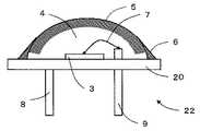
本発明に係る第1の実施形態の白色LED発光装置では、図1に示すように、蛍光体の励起光源であるLEDチップ3を搭載した基板20上をドーム状(たとえば半球状)に満たした透明樹脂層(透明樹脂部)4を有し、その透明樹脂層4の外側に蛍光体層5を持つ。半球状の透明樹脂層4の基板20との境界に近い部分にはその外側に蛍光体層5が存在しない環状の領域があり、この領域を覆うように反射層6が形成されている。LEDチップ3は金ワイヤボンディング7などによってリードフレーム22上の電極8,9に接続されている。[First Embodiment]
In the white LED light emitting device of the first embodiment according to the present invention, as shown in FIG. 1, the
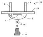
この構造の製造方法は、たとえば、図2ないし図4に示すような手順となる。まず、基板20上にLEDチップ3を実装する。そして、図2に示すように、基板20のLEDチップ3が実装された面を下にした状態で、基板20上に、蛍光体含有透明樹脂11を塗布し、蛍光体含有透明樹脂11のドーム状の構造を形成する。このとき、液滴吐出装置10から上向きに樹脂の液滴を吐出させる。つぎに、蛍光体含有透明樹脂11が硬化する前に、その中に含有されている蛍光体を沈降させて、図3に示すように、ドーム状の構造の表面近くに蛍光体が多く集まった蛍光体層5を形成させ、その内側の透明樹脂層4と分離させる。その後に透明樹脂を硬化させる。 The manufacturing method of this structure is, for example, a procedure as shown in FIGS. First, the
つぎに、図4に示すように、透明樹脂層4が基板20に接する付近を囲むように環状の反射層6を形成する。このとき、蛍光体含有透明樹脂11の塗布と同様に、液滴吐出装置10から上向きに金属含有インクを吐出することによって、反射層6を塗布形成することができる。 Next, as shown in FIG. 4, an
上記説明では、蛍光体含有透明樹脂11のドーム状の構造を形成した後に、蛍光体を沈降させて蛍光体層5を形成させることとしたが、他の方法として、はじめに透明樹脂のみによる小半球構造をLEDチップ3上に形成し、その後に蛍光体含有透明樹脂層を重ねて形成してもよい。 In the above description, after forming the dome-shaped structure of the phosphor-containing
このようにして、LEDチップ3から蛍光体を隔離させ、半球状の透明樹脂層4の表層部に蛍光体層5を形成することができる。蛍光体の沈降は、より粒子径の大きいものほど沈降速度が速くなる。したがって、形成された蛍光体層内では、半球構造の外向きに、粒子径がより大きくなる分布をもつ構造となる。沈降によって形成されるこの蛍光体粒子層では、より粒子径の大きい粒子から半球構造の表層に堆積していくことから、大粒子によって構成された空隙を小粒子が埋めていくように堆積することになる。したがって、蛍光体層の厚みのむらが小さくなる。 In this way, the phosphor can be isolated from the
ここでの基板20は、リードフレーム22のLEDチップ3搭載部でもよい。また、セラミック平面基板でもよいし、ガラス平面基板でもよい。 The
本製造プロセスとしては、特に高速の製造プロセスを考慮した場合、半球状の透明樹脂内において蛍光体粒子が迅速に沈降することが望ましい。透明樹脂層4の粘度が低いほど蛍光体の沈降速度は大きくなることから、沈降速度の面からは、透明樹脂層の粘度が低い方が望ましい。また、液滴吐出装置10においては、一般的に、高粘度の液体を吐出することは困難であり、吐出性の観点からも、より低粘度であることが望ましい。 As this manufacturing process, it is desirable that the phosphor particles settle quickly in the hemispherical transparent resin, particularly considering a high-speed manufacturing process. The lower the viscosity of the
液滴吐出装置によって吐出する蛍光体含有透明樹脂11における蛍光体の含有率は、たとえば蛍光体粒子径が約30μmの場合、15重量%から60重量%の範囲であることが望ましい。同じ蛍光体の重量%の蛍光体含有透明樹脂を用い、同じ青色LEDチップを用いた場合、形成する半球構造の大きさが大きくなるほど、黄色蛍光体の量が過剰となる傾向があり、より黄色味を帯びた発光となる。半球構造の直径が約1mmの場合、蛍光体の濃度は40〜50重量%であることが望ましい。 The phosphor content in the phosphor-containing
この実施形態における液滴吐出装置10としては、プリンタなどに利用されるインクジェット装置を利用することができる。一般的に、ピエゾ方式や、サーマル方式の液滴吐出装置では、ノズル部の詰まりの問題などから、約30mPa・s以下の低粘度のインクや、小粒子径の粒子を含有したインクを安定に吐出することしかできない。一方、集束超音波方式の液滴吐出装置(特許文献4および5参照)においては、インクつまりの原因であるノズルが不要である構成であることから、より高粘度のインクや、数十ミクロン径の粒子を含有した液滴を吐出することができる。したがって、集束超音波方式の液滴吐出装置によって、白色LEDのパッケージングに用いられる、高粘度(>100mPa・s)の樹脂や、10μm径以上の蛍光体粒子を含有した樹脂液滴を吐出することができる。 As the
本実施形態において、透明樹脂および蛍光体粒子の吐出に超音波液滴吐出装置を用いることを前提とした場合、透明樹脂の粘度は、3000mPa・s以下が望ましく、安定したパターニング性を考慮した場合は1000mPa・s以下であることがより望ましい。一方、液滴吐出装置のインク室内での蛍光体の分散性は高いほうが望ましく、それには粘度が高いほうが蛍光体の沈降性が抑えられるために望ましい。したがって、この観点からは、透明樹脂の粘度は100mPa・s以上であることが望ましい。 In the present embodiment, when it is assumed that an ultrasonic droplet discharge device is used for discharging transparent resin and phosphor particles, the viscosity of the transparent resin is desirably 3000 mPa · s or less, and considering stable patterning properties Is more preferably 1000 mPa · s or less. On the other hand, it is desirable that the phosphor is highly dispersible in the ink chamber of the droplet discharge device, and that a higher viscosity is desirable because the sedimentation property of the phosphor is suppressed. Therefore, from this viewpoint, the viscosity of the transparent resin is desirably 100 mPa · s or more.
透明樹脂の種類としては、液滴吐出装置による吐出時においては低粘度であり、基板20への樹脂の着弾後に硬化することが可能なものが望ましい。具体的には、熱硬化型のシリコーン樹脂、または熱硬化型のエポキシ樹脂が望ましい。ただし、エポキシ樹脂などの有機高分子系材料は、LEDチップ光源による材料劣化が起こりやすく、長時間使用した際に、着色などの劣化を生じることがある。したがって、熱硬化型のシリコーン樹脂を用いることが望ましい。 As the type of the transparent resin, it is preferable that the transparent resin has a low viscosity when discharged by the droplet discharge device and can be cured after the resin has landed on the
熱硬化型樹脂は、一液型、二液混合型いずれでもよい。また、熱硬化型樹脂は、基板20を加熱することによって、樹脂の硬化を促進することができることから、基板20の加熱によって、蛍光体の沈降速度を遅らせることができる。これにより、半球構造内での蛍光体分布の調整を行なうことができる。 The thermosetting resin may be either a one-component type or a two-component mixed type. In addition, since the thermosetting resin can accelerate the curing of the resin by heating the
蛍光体材料としては、沈降による蛍光体層を迅速に形成する必要があることから、粒子径が大きい方が望ましい。また、白色LED構造における光取り出し効率としては、蛍光体の粒子径が大きい方が向上する傾向があることから、発光装置としても、蛍光体の粒子径はより大きい方が望ましい。一方、粒子径が大きいほど、液滴吐出装置におけるインク室内での粒子分散性は低下し、また液滴吐出装置での吐出はより困難なものとなる。これらの要因を総合して、蛍光体の粒子径は5μm〜100μmの範囲であることが望ましい。 As the phosphor material, it is desirable that the particle diameter is large because it is necessary to quickly form a phosphor layer by sedimentation. Also, as the light extraction efficiency in the white LED structure, the larger the particle diameter of the phosphor tends to be improved, the larger the particle diameter of the phosphor is desirable for the light emitting device. On the other hand, the larger the particle diameter, the lower the particle dispersibility in the ink chamber of the droplet discharge device, and the more difficult the discharge with the droplet discharge device. In consideration of these factors, the particle diameter of the phosphor is preferably in the range of 5 μm to 100 μm.
本実施形態での、蛍光体の沈降を利用した蛍光体層の形成方法においては、半球構造での基板20近傍部において、蛍光体がほとんど分布しない領域が形成される。この部分からはLEDチップからの青色光が漏洩し、その結果、白色LED発光装置としては色むらを生じることになる。一般的に白色LEDでは、発光装置の上方への光取り出しを高めるために、LEDチップの周辺に反射板を設置した構造を有している。 In the method for forming a phosphor layer using phosphor sedimentation in this embodiment, a region in which the phosphor is hardly distributed is formed in the vicinity of the
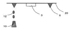
本実施形態での白色LED発光装置の半球構造における基板20近傍部において、半球の外部から反射層6を設置することにより、この色むらの課題は大幅に改善される。この場合、青色光の漏洩を防ぐためには、反射層6は、半球構造に接している必要がある。したがって、立体的な半球構造の側部に接した反射層6を設置する方法として、液滴吐出装置による金属含有インクを塗布するという方法が適している。金属含有インクとして代表的なものは、金、銀、銅などのナノサイズの粒子を分散させたインクがある。反射率や粒子の安定性などから、銀粒子含有のインクが反射層形成のためにより望ましい。 By installing the
作成手順としては、半球構造の形成後に、液滴吐出装置10によって半球構造の側面に金属含有インクを塗布する。金属含有インクには、ナノ粒子を安定に分散させるための分散剤が含まれており、塗布後加熱焼成することによって、より反射率の高い反射層を得ることができる。ここで低温焼成タイプの銀ナノコロイド含有インクを用いると、150℃の焼成によって十分な反射率を有する反射層が形成できる。焼成時に、反射層にクラックが入った場合、重ねて金属含有インクを塗布、焼成することによってクラックを埋めることができる。 As a preparation procedure, after the formation of the hemispherical structure, a metal-containing ink is applied to the side surface of the hemispherical structure by the
蛍光体を沈降させることによって蛍光体層5を形成する際に、半球構造の径は、より小さい方が膜厚の均一な蛍光体層5を形成する上で望ましい。半球構造の径が大きくなるにつれて、半球構造の先端部にのみ蛍光体が集中しやすくなる。しかしながら、基板20上に、低粘度の透明樹脂を塗布した場合、透明樹脂の基板20との親和性が高い場合、基板20上に容易に広がってしまい、所望の大きさの半球構造を形成することは非常に困難である。 When forming the
この樹脂の広がりを抑制する方法として、熱硬化樹脂を用いた場合に基板20の加熱を行なうという方法が考えられる。しかし、あまり樹脂の硬化が早いと、沈降による蛍光体層5の形成が不十分となり、本実施形態での発光装置構造の特徴が不十分なものとなる。そこで、所望の大きさの半球構造を得るための方法として、一つは、リードフレーム22の樹脂形成部の直径を小径化することが挙げられる。これにより、半球構造は、樹脂形成部の直径と等しくなり、樹脂の広がりを押さえることができる。しかし、この方法は、一般的な平面基板20上への白色LED発光装置作成への応用はできない。 As a method for suppressing the spread of the resin, a method of heating the
もう一つは、基板20部の表面エネルギーを下げることによって、透明樹脂の着弾後の広がりを抑える方法である。たとえば、透明樹脂を塗布する前の基板20部の表面に撥水処理を施す。この方法により、液滴吐出装置10によって着弾した透明樹脂は基板20との大きな接触角をもつことによって、着弾した樹脂量に応じた径の半球構造を形成することができる。基板20表面の撥水処理として、たとえば、基板20表面にフッ素系ポリマーをコートする方法などがある。 The other is a method of suppressing the spread of the transparent resin after landing by lowering the surface energy of 20 parts of the substrate. For example, a water repellent treatment is performed on the surface of 20 parts of the substrate before applying the transparent resin. By this method, the transparent resin landed by the
実験では、金メッキ被覆したリードフレーム上での表面処理品において、シリコーン樹脂に対して接触角約60度の半球構造が得られた。一方、無処理品においては、シリコーンは不規則に基板20上に広がり、LEDチップを被覆することも困難であった。用いる表面処理剤は、たとえばフッ素系ポリマーを含有した離型剤を用い、基板20に対して、離型剤の溶液をディップコートあるいはスピンコートすることによって表面処理を行なう。 In the experiment, a hemispherical structure having a contact angle of about 60 degrees with respect to the silicone resin was obtained in the surface-treated product on the lead frame coated with gold. On the other hand, in the untreated product, the silicone spreads irregularly on the
以上説明したように、本実施形態によれば、発光チップと蛍光体層との接触のない発光装置構造を実現でき、厚みの均一性の高い蛍光体層を得ることができ、その結果、色むらの少ない白色LED発光装置を得ることができる。また、蛍光体の沈降現象を利用しているために、透明樹脂層と蛍光体層との二層構造の形成を、液滴吐出装置による塗布の一プロセスによって行なうことが可能であり、従来の製法と比較して簡便な製造プロセスとなる。 As described above, according to the present embodiment, a light emitting device structure without contact between the light emitting chip and the phosphor layer can be realized, and a phosphor layer with high uniformity in thickness can be obtained. A white LED light emitting device with less unevenness can be obtained. In addition, since the phosphor sedimentation phenomenon is utilized, the two-layer structure of the transparent resin layer and the phosphor layer can be formed by a single coating process using a droplet discharge device. It becomes a simple manufacturing process compared with a manufacturing method.
[第2の実施形態]
図5ないし図7に示すように、上記と同様の白色LED発光装置構造を、作成工程の順序を変えて行なうこともできる。すなわち、はじめに基板上にLEDチップ3を搭載し、その後、図5に示すように、液滴吐出装置10により、金属含有インク12を平面基板20上に環状に塗布することによって、反射層6を形成する。このとき、特に、超音波方式の液滴吐出装置10を用いて高粘度の金属含有インクを上向きに吐出しながら塗布することによって、基板20の垂直方向に厚みを持つ反射層6の立体構造を得ることが容易になる。[Second Embodiment]
As shown in FIGS. 5 to 7, a white LED light emitting device structure similar to the above can be performed by changing the order of the production steps. That is, the
続いて、図6に示すように、基板20上のLEDチップ上に蛍光体含有透明樹脂11を吐出し、ドームを形成する。その後、蛍光体が沈降した後、透明樹脂を硬化させる。これにより、図7に示すような白色LED発光装置構造を得ることができる。この製法によると、第1の実施形態に比べて、反射層6の透明樹脂層4に接する反射面の向きが、LEDチップ3からの光を、より蛍光体層5の向きに反射する向きとなるため、光の取り出しという意味でも有利な構造となる。 Subsequently, as shown in FIG. 6, the phosphor-containing
[第3の実施形態]
本発明の作成方法を、反射板を有するパッケージカップを用いた発光装置の作成に応用することもできる。その構造を図8に示す。この実施形態においては、平板基板の代わりに、窪み31が形成されたパッケージカップ30を用い、窪み31の底部32中央にLEDチップ3を設置する。そして、LEDチップ3の外側に半球状の透明樹脂層4と蛍光体層5を形成し、透明樹脂層4と窪み31の底部32の境界部付近に環状に反射層6を形成する。[Third Embodiment]
The production method of the present invention can also be applied to production of a light emitting device using a package cup having a reflector. The structure is shown in FIG. In this embodiment, instead of a flat substrate, a
ここで、透明樹脂層4および蛍光体層5の形成、および反射層6の形成に当たっては、第1または第2の実施形態と同様に、LEDチップ3が設置されたパッケージカップ30の窪み31を下向きにして、液滴吐出装置10から液滴を上向きに吐出することによって行なう。 Here, in the formation of the
このとき、窪み31の底部32の表面エネルギーを下げるために底部32の表面に撥水処理を施しても良い。蛍光体が半球状の透明樹脂層内で沈降することにより半球状の透明樹脂層4と蛍光体層5を形成する。液滴吐出装置10によって金属含有インクを透明樹脂層の側部に塗布することにより、反射層6を形成することも第1または第2の実施形態と同様である。 At this time, in order to lower the surface energy of the
この第3の本実施形態の場合、パッケージカップ30の窪み31の側面によって反射板1が形成されているこれにより、発光装置上方への光の集光性が高まる効果が得られる。 In the case of the third embodiment, the reflecting
[第4の実施形態]
本発明の第4の実施形態に係る発光装置は、図9に示すように、基板20上に配置された紫外LEDチップ3と、紫外LEDチップ3を覆うように配置されたドーム状(たとえば半球状)の透明樹脂層4と、その外側を覆う赤色蛍光体層13とを有する。この実施形態ではさらにこの赤色蛍光体層13の外側に、第2の透明樹脂層4a、緑色蛍光体層14、第3の透明樹脂層4b、青色蛍光体層15が順次形成されている。[Fourth Embodiment]
As shown in FIG. 9, the light emitting device according to the fourth embodiment of the present invention includes an
この第4の実施形態は、特許文献3に開示された白色LED構造に本発明を適用するものである。すなわち、紫外LEDチップ3から発せられた紫外線を、赤色蛍光体層13、緑色蛍光体層14、青色蛍光体層15に順次通して白色光を得るものである。この場合に、かりに赤、青、緑色蛍光体を混合して半球状に形成した場合、一般に、短波長側の光が吸収されてしまいやすい。そのため、この実施形態では、より短波長発光の蛍光体の層を外層に位置するように積層する。 In the fourth embodiment, the present invention is applied to a white LED structure disclosed in
つぎに、この第4実施形態の発光装置の製造方法について説明する。はじめに、紫外LEDチップ3を基板20上に搭載し、この発光チップ3の搭載された基板20を下向きにした状態で、液滴吐出装置10によって、発光チップ3に向けて、赤色蛍光体粒子を含有した透明樹脂液滴を上向きに吐出し、基板20上に半球構造を形成する。そして、赤色蛍光体層13が半球構造の表面近くに沈降した後に、透明樹脂を加熱硬化させ、透明樹脂層4とその外側の赤色蛍光体層13を形成する。硬化後、重ねて緑色蛍光体含有樹脂を同様に塗布、硬化させて、赤色蛍光体層13の外側に、第2の透明樹脂層4aとその外側の緑色蛍光体層14を形成する。その硬化後に、さらにその外側に重ねて第3の透明樹脂層4bとその外側の青色蛍光体層15を形成する。 Next, a method for manufacturing the light emitting device of the fourth embodiment will be described. First, with the
この作成手順により、透明樹脂層4、赤色蛍光体層13、第2の透明樹脂層4a、緑色蛍光体層14、第3の透明樹脂層4b、青色蛍光体層15、といった6層の多層構造が形成される。この構造により、蛍光体の色間での光吸収を抑えた白色LEDの形成が可能となる。 By this preparation procedure, a multilayer structure of six layers including the
1:反射板、 3:LEDチップ、 4,4a,4b:透明樹脂層(透明樹脂部)、 5:蛍光体層、 6:反射層、 7:金ワイヤボンディング、 8,9:電極、 10:液滴吐出装置、 11:蛍光体含有透明樹脂、 12:金属含有インク、 13:赤色蛍光体層、 14:緑色蛍光体層、 15:青色蛍光体層、 20:基板、 22:リードフレーム、 30:パッケージカップ、 31:窪み、 32:底部1: Reflector, 3: LED chip, 4, 4a, 4b: Transparent resin layer (transparent resin part), 5: Phosphor layer, 6: Reflective layer, 7: Gold wire bonding, 8, 9: Electrode, 10: Droplet discharge device, 11: phosphor-containing transparent resin, 12: metal-containing ink, 13: red phosphor layer, 14: green phosphor layer, 15: blue phosphor layer, 20: substrate, 22: lead frame, 30 : Package cup, 31: Dimple, 32: Bottom
Claims (8)
Translated fromJapanese前記基板の上で前記発光チップの外側を満たしてドーム状に覆う透明樹脂部および、蛍光体を含有して前記透明樹脂部の少なくとも頂部付近の外側に形成される蛍光体層を、液滴吐出装置を用いて形成するドーム形成ステップと、
前記ドーム状の透明樹脂部および蛍光体層の外側で前記基板に接する位置付近に反射層を形成する反射層形成ステップと、
を有し、前記ドーム形成ステップは、
前記基板の上および前記発光チップの外側に向けて透明樹脂の液滴を前記液滴吐出装置によって上向きに吐出させる透明樹脂吐出ステップと、
前記透明樹脂吐出ステップの後に蛍光体を含有する透明樹脂の液滴を前記液滴吐出装置によって上向きに吐出させる蛍光体含有樹脂吐出ステップと、
を含むこと、を特徴とする発光装置製造方法。A mounting step of mounting the light emitting chip on the substrate;
A transparent resin portion that fills the outside of the light emitting chip on the substrate and covers it in a dome shape, and a phosphor layer that contains the phosphor and is formed on the outside at least near the top of the transparent resin portion, droplet discharge A dome forming step formed using the apparatus;
A reflective layer forming step of forming a reflective layer near the position in contact with the substrate outside the dome-shaped transparent resin portion and the phosphor layer;
Have a, the doming step,
A transparent resin discharging step of discharging a transparent resin droplet upward by the droplet discharging device toward the substrate and the outside of the light emitting chip;
A phosphor-containing resin discharging step in which the transparent resin droplets containing the phosphor are discharged upward by the droplet discharging device after the transparent resin discharging step;
A method for manufacturing a light emitting device.
前記基板の上および前記発光チップの外側に向けて蛍光体を含有する透明樹脂の液滴を上向きに吐出させる蛍光体含有樹脂吐出ステップと、
前記蛍光体含有樹脂吐出ステップによって吐出された透明樹脂が硬化する前に当該透明樹脂中の前記蛍光体を前記ドームの表面近くに沈降させる沈降ステップと、
を含むこと、を特徴とする請求項1に記載の発光装置製造方法。The dome forming step includes
A phosphor-containing resin discharge step of discharging a transparent resin droplet containing the phosphor upward on the substrate and toward the outside of the light emitting chip;
A sedimentation step of allowing the phosphor in the transparent resin to settle near the surface of the dome before the transparent resin discharged by the phosphor-containing resin discharging step is cured;
The method for manufacturing a light emitting device according to claim 1, comprising:
Priority Applications (5)
| Application Number | Priority Date | Filing Date | Title |
|---|---|---|---|
| JP2007132552AJP5006102B2 (en) | 2007-05-18 | 2007-05-18 | Light emitting device and manufacturing method thereof |
| US12/122,472US7839087B2 (en) | 2007-05-18 | 2008-05-16 | Light emitting device and method of manufacturing the same |
| CN200810099493.3ACN101308898B (en) | 2007-05-18 | 2008-05-16 | Light emitting device and manufacturing method thereof |
| EP08156366AEP1993151A3 (en) | 2007-05-18 | 2008-05-16 | Light emitting device and method of manufacturing the same |
| US12/923,949US8419497B2 (en) | 2007-05-18 | 2010-10-15 | Light emitting device and method of manufacturing the same |
Applications Claiming Priority (1)
| Application Number | Priority Date | Filing Date | Title |
|---|---|---|---|
| JP2007132552AJP5006102B2 (en) | 2007-05-18 | 2007-05-18 | Light emitting device and manufacturing method thereof |
Publications (2)
| Publication Number | Publication Date |
|---|---|
| JP2008288409A JP2008288409A (en) | 2008-11-27 |
| JP5006102B2true JP5006102B2 (en) | 2012-08-22 |
Family
ID=39645367
Family Applications (1)
| Application Number | Title | Priority Date | Filing Date |
|---|---|---|---|
| JP2007132552AExpired - Fee RelatedJP5006102B2 (en) | 2007-05-18 | 2007-05-18 | Light emitting device and manufacturing method thereof |
Country Status (4)
| Country | Link |
|---|---|
| US (2) | US7839087B2 (en) |
| EP (1) | EP1993151A3 (en) |
| JP (1) | JP5006102B2 (en) |
| CN (1) | CN101308898B (en) |
Families Citing this family (75)
| Publication number | Priority date | Publication date | Assignee | Title |
|---|---|---|---|---|
| US9412926B2 (en) | 2005-06-10 | 2016-08-09 | Cree, Inc. | High power solid-state lamp |
| JP5006102B2 (en)* | 2007-05-18 | 2012-08-22 | 株式会社東芝 | Light emitting device and manufacturing method thereof |
| JP2008288410A (en)* | 2007-05-18 | 2008-11-27 | Toshiba Corp | Semiconductor light emitting device and manufacturing method thereof |
| US8118447B2 (en) | 2007-12-20 | 2012-02-21 | Altair Engineering, Inc. | LED lighting apparatus with swivel connection |
| US8360599B2 (en) | 2008-05-23 | 2013-01-29 | Ilumisys, Inc. | Electric shock resistant L.E.D. based light |
| US7938562B2 (en) | 2008-10-24 | 2011-05-10 | Altair Engineering, Inc. | Lighting including integral communication apparatus |
| US8653984B2 (en) | 2008-10-24 | 2014-02-18 | Ilumisys, Inc. | Integration of LED lighting control with emergency notification systems |
| US8901823B2 (en) | 2008-10-24 | 2014-12-02 | Ilumisys, Inc. | Light and light sensor |
| US8214084B2 (en) | 2008-10-24 | 2012-07-03 | Ilumisys, Inc. | Integration of LED lighting with building controls |
| US8324817B2 (en) | 2008-10-24 | 2012-12-04 | Ilumisys, Inc. | Light and light sensor |
| US8507300B2 (en)* | 2008-12-24 | 2013-08-13 | Ledengin, Inc. | Light-emitting diode with light-conversion layer |
| TWI380483B (en)* | 2008-12-29 | 2012-12-21 | Everlight Electronics Co Ltd | Led device and method of packaging the same |
| TWI463708B (en)* | 2009-02-24 | 2014-12-01 | Advanced Optoelectronic Tech | Side light-emitting type light-emitting element package structure and manufacturing method thereof |
| US8330381B2 (en)* | 2009-05-14 | 2012-12-11 | Ilumisys, Inc. | Electronic circuit for DC conversion of fluorescent lighting ballast |
| US8299695B2 (en)* | 2009-06-02 | 2012-10-30 | Ilumisys, Inc. | Screw-in LED bulb comprising a base having outwardly projecting nodes |
| EP2446190A4 (en)* | 2009-06-23 | 2013-02-20 | Ilumisys Inc | LED LAMP WITH WAVELENGTH CONVERSION LAYER |
| KR101186648B1 (en)* | 2009-12-21 | 2012-09-28 | 서울반도체 주식회사 | Light emitting diode package and method for fabricating the same diode |
| JP2011159770A (en)* | 2010-01-29 | 2011-08-18 | Yamaguchi Univ | White-light emitting semiconductor device |
| JP2011159832A (en)* | 2010-02-01 | 2011-08-18 | Yamaguchi Univ | Semiconductor light emitting device |
| JP5678629B2 (en)* | 2010-02-09 | 2015-03-04 | ソニー株式会社 | Method for manufacturing light emitting device |
| CN102155635A (en)* | 2010-02-11 | 2011-08-17 | 亿光电子工业股份有限公司 | Light emitting diode module |
| US8931933B2 (en) | 2010-03-03 | 2015-01-13 | Cree, Inc. | LED lamp with active cooling element |
| US9062830B2 (en) | 2010-03-03 | 2015-06-23 | Cree, Inc. | High efficiency solid state lamp and bulb |
| US8882284B2 (en) | 2010-03-03 | 2014-11-11 | Cree, Inc. | LED lamp or bulb with remote phosphor and diffuser configuration with enhanced scattering properties |
| US9316361B2 (en) | 2010-03-03 | 2016-04-19 | Cree, Inc. | LED lamp with remote phosphor and diffuser configuration |
| US9057511B2 (en) | 2010-03-03 | 2015-06-16 | Cree, Inc. | High efficiency solid state lamp and bulb |
| US10359151B2 (en) | 2010-03-03 | 2019-07-23 | Ideal Industries Lighting Llc | Solid state lamp with thermal spreading elements and light directing optics |
| US9024517B2 (en) | 2010-03-03 | 2015-05-05 | Cree, Inc. | LED lamp with remote phosphor and diffuser configuration utilizing red emitters |
| US9625105B2 (en) | 2010-03-03 | 2017-04-18 | Cree, Inc. | LED lamp with active cooling element |
| US8562161B2 (en) | 2010-03-03 | 2013-10-22 | Cree, Inc. | LED based pedestal-type lighting structure |
| US9310030B2 (en) | 2010-03-03 | 2016-04-12 | Cree, Inc. | Non-uniform diffuser to scatter light into uniform emission pattern |
| US9275979B2 (en) | 2010-03-03 | 2016-03-01 | Cree, Inc. | Enhanced color rendering index emitter through phosphor separation |
| US8632196B2 (en) | 2010-03-03 | 2014-01-21 | Cree, Inc. | LED lamp incorporating remote phosphor and diffuser with heat dissipation features |
| US9500325B2 (en) | 2010-03-03 | 2016-11-22 | Cree, Inc. | LED lamp incorporating remote phosphor with heat dissipation features |
| JP2013521647A (en)* | 2010-03-03 | 2013-06-10 | クリー インコーポレイテッド | Radiators with improved color rendering index through phosphor separation |
| CA2792940A1 (en) | 2010-03-26 | 2011-09-19 | Ilumisys, Inc. | Led light with thermoelectric generator |
| CA2794512A1 (en) | 2010-03-26 | 2011-09-29 | David L. Simon | Led light tube with dual sided light distribution |
| US8540401B2 (en)* | 2010-03-26 | 2013-09-24 | Ilumisys, Inc. | LED bulb with internal heat dissipating structures |
| US9039216B2 (en) | 2010-04-01 | 2015-05-26 | Lg Innotek Co., Ltd. | Light emitting device package and light unit having the same |
| US8454193B2 (en) | 2010-07-08 | 2013-06-04 | Ilumisys, Inc. | Independent modules for LED fluorescent light tube replacement |
| CA2803267A1 (en) | 2010-07-12 | 2012-01-19 | Ilumisys, Inc. | Circuit board mount for led light tube |
| US10451251B2 (en) | 2010-08-02 | 2019-10-22 | Ideal Industries Lighting, LLC | Solid state lamp with light directing optics and diffuser |
| EP2633227B1 (en) | 2010-10-29 | 2018-08-29 | iLumisys, Inc. | Mechanisms for reducing risk of shock during installation of light tube |
| US8870415B2 (en) | 2010-12-09 | 2014-10-28 | Ilumisys, Inc. | LED fluorescent tube replacement light with reduced shock hazard |
| EP2472578B1 (en)* | 2010-12-28 | 2020-06-03 | Nichia Corporation | Light emitting device |
| KR101923588B1 (en)* | 2011-01-21 | 2018-11-29 | 스탠리 일렉트릭 컴퍼니, 리미티드 | Light-Emitting Device, Method for Producing The Same, and Illuminating Device |
| US9068701B2 (en) | 2012-01-26 | 2015-06-30 | Cree, Inc. | Lamp structure with remote LED light source |
| US9234655B2 (en) | 2011-02-07 | 2016-01-12 | Cree, Inc. | Lamp with remote LED light source and heat dissipating elements |
| JP5899623B2 (en)* | 2011-02-10 | 2016-04-06 | 三菱マテリアル株式会社 | Laminate for solder joint and joined body |
| US11251164B2 (en) | 2011-02-16 | 2022-02-15 | Creeled, Inc. | Multi-layer conversion material for down conversion in solid state lighting |
| CN102683555A (en)* | 2011-03-07 | 2012-09-19 | 展晶科技(深圳)有限公司 | Packaging structure and packaging method for light-emitting diode |
| US8754440B2 (en)* | 2011-03-22 | 2014-06-17 | Tsmc Solid State Lighting Ltd. | Light-emitting diode (LED) package systems and methods of making the same |
| JP5919504B2 (en)* | 2011-06-30 | 2016-05-18 | パナソニックIpマネジメント株式会社 | Light emitting device |
| US9072171B2 (en) | 2011-08-24 | 2015-06-30 | Ilumisys, Inc. | Circuit board mount for LED light |
| JP5988073B2 (en)* | 2011-11-01 | 2016-09-07 | 東芝ライテック株式会社 | Light emitting module and lighting device |
| CN103165791A (en)* | 2011-12-16 | 2013-06-19 | 并日电子科技(深圳)有限公司 | Substrate for light emitting diode element and light emitting diode component with same |
| CN103296182B (en)* | 2012-03-01 | 2016-09-21 | 展晶科技(深圳)有限公司 | Light-emitting diode lamp source device |
| US9184518B2 (en) | 2012-03-02 | 2015-11-10 | Ilumisys, Inc. | Electrical connector header for an LED-based light |
| US9488359B2 (en) | 2012-03-26 | 2016-11-08 | Cree, Inc. | Passive phase change radiators for LED lamps and fixtures |
| JP5677371B2 (en)* | 2012-06-04 | 2015-02-25 | 株式会社東芝 | Light emitting device |
| US9163794B2 (en) | 2012-07-06 | 2015-10-20 | Ilumisys, Inc. | Power supply assembly for LED-based light tube |
| US9271367B2 (en) | 2012-07-09 | 2016-02-23 | Ilumisys, Inc. | System and method for controlling operation of an LED-based light |
| WO2014026486A1 (en)* | 2012-08-17 | 2014-02-20 | Qian Zhiqiang | Led light-emitting device for white light |
| US9285084B2 (en) | 2013-03-14 | 2016-03-15 | Ilumisys, Inc. | Diffusers for LED-based lights |
| DE102013103983B4 (en) | 2013-04-19 | 2021-09-23 | OSRAM Opto Semiconductors Gesellschaft mit beschränkter Haftung | Process for the production of a large number of radiation-emitting semiconductor chips |
| US9267650B2 (en) | 2013-10-09 | 2016-02-23 | Ilumisys, Inc. | Lens for an LED-based light |
| CN106063381A (en) | 2014-01-22 | 2016-10-26 | 伊卢米斯公司 | LED-based light with addressed LEDs |
| US9360188B2 (en) | 2014-02-20 | 2016-06-07 | Cree, Inc. | Remote phosphor element filled with transparent material and method for forming multisection optical elements |
| US9510400B2 (en) | 2014-05-13 | 2016-11-29 | Ilumisys, Inc. | User input systems for an LED-based light |
| JP6248881B2 (en)* | 2014-09-22 | 2017-12-20 | トヨタ紡織株式会社 | Composite membrane and manufacturing method thereof |
| KR102227774B1 (en) | 2014-10-23 | 2021-03-16 | 삼성전자주식회사 | Method for manufacturing light emitting diode package |
| DE102015107516A1 (en)* | 2015-05-13 | 2016-11-17 | Osram Opto Semiconductors Gmbh | Method for producing a lens for an optoelectronic lighting device |
| US10161568B2 (en) | 2015-06-01 | 2018-12-25 | Ilumisys, Inc. | LED-based light with canted outer walls |
| JP6800702B2 (en)* | 2016-11-08 | 2020-12-16 | スタンレー電気株式会社 | Semiconductor light emitting device and its manufacturing method |
| JP7226131B2 (en)* | 2019-06-25 | 2023-02-21 | 豊田合成株式会社 | Light emitting device and manufacturing method thereof |
Family Cites Families (25)
| Publication number | Priority date | Publication date | Assignee | Title |
|---|---|---|---|---|
| JPS5650587A (en)* | 1979-10-02 | 1981-05-07 | Nec Corp | Manufacture of light emitting diode |
| JPH06238884A (en) | 1992-12-22 | 1994-08-30 | Xerox Corp | Acoustic liquid drip ejector and its production |
| JPH0799345A (en) | 1993-09-28 | 1995-04-11 | Nichia Chem Ind Ltd | Light emitting diode |
| JP3432914B2 (en)* | 1994-09-30 | 2003-08-04 | 株式会社東芝 | Ink jet recording device |
| JP3584163B2 (en)* | 1998-07-27 | 2004-11-04 | サンケン電気株式会社 | Method for manufacturing semiconductor light emitting device |
| US5959316A (en)* | 1998-09-01 | 1999-09-28 | Hewlett-Packard Company | Multiple encapsulation of phosphor-LED devices |
| JP2000156528A (en)* | 1998-11-19 | 2000-06-06 | Sharp Corp | Light emitting element |
| JP4412787B2 (en)* | 1999-06-09 | 2010-02-10 | 三洋電機株式会社 | Irradiation device and irradiation module using metal substrate |
| US7091656B2 (en)* | 2001-04-20 | 2006-08-15 | Nichia Corporation | Light emitting device |
| KR100510423B1 (en)* | 2001-06-01 | 2005-08-30 | 세이코 엡슨 가부시키가이샤 | Color filter, display unit and electronic apparatus |
| JP4789350B2 (en) | 2001-06-11 | 2011-10-12 | シチズン電子株式会社 | Manufacturing method of light emitting diode |
| US6576488B2 (en) | 2001-06-11 | 2003-06-10 | Lumileds Lighting U.S., Llc | Using electrophoresis to produce a conformally coated phosphor-converted light emitting semiconductor |
| CN1211869C (en)* | 2002-08-12 | 2005-07-20 | 财团法人工业技术研究院 | Light emitting diode packaging structure and method thereof |
| JP2004087812A (en)* | 2002-08-27 | 2004-03-18 | Sanyo Electric Co Ltd | Light emitting device |
| JP2004119583A (en) | 2002-09-25 | 2004-04-15 | Seiko Epson Corp | Optical element manufacturing method |
| JP2004273798A (en)* | 2003-03-10 | 2004-09-30 | Toyoda Gosei Co Ltd | Light emitting device |
| KR100609830B1 (en)* | 2003-04-25 | 2006-08-09 | 럭스피아 주식회사 | White semiconductor light emitting device using green and red phosphors |
| JP3719441B2 (en)* | 2003-08-01 | 2005-11-24 | セイコーエプソン株式会社 | Optical element and method for manufacturing the same, optical module, and optical transmission device |
| KR100610249B1 (en)* | 2003-12-23 | 2006-08-09 | 럭스피아 주식회사 | Yellow light emitting phosphor and white semiconductor light emitting device using the same |
| US7344902B2 (en)* | 2004-11-15 | 2008-03-18 | Philips Lumileds Lighting Company, Llc | Overmolded lens over LED die |
| JP2007049114A (en)* | 2005-05-30 | 2007-02-22 | Sharp Corp | Light emitting device and manufacturing method thereof |
| JP3979424B2 (en)* | 2005-09-09 | 2007-09-19 | 松下電工株式会社 | Light emitting device |
| EP1928029B1 (en)* | 2005-09-20 | 2018-10-31 | Panasonic Intellectual Property Management Co., Ltd. | Light emitting diode package |
| JP2008288410A (en) | 2007-05-18 | 2008-11-27 | Toshiba Corp | Semiconductor light emitting device and manufacturing method thereof |
| JP5006102B2 (en) | 2007-05-18 | 2012-08-22 | 株式会社東芝 | Light emitting device and manufacturing method thereof |
- 2007
- 2007-05-18JPJP2007132552Apatent/JP5006102B2/ennot_activeExpired - Fee Related
- 2008
- 2008-05-16CNCN200810099493.3Apatent/CN101308898B/ennot_activeExpired - Fee Related
- 2008-05-16EPEP08156366Apatent/EP1993151A3/ennot_activeWithdrawn
- 2008-05-16USUS12/122,472patent/US7839087B2/ennot_activeExpired - Fee Related
- 2010
- 2010-10-15USUS12/923,949patent/US8419497B2/ennot_activeExpired - Fee Related
Also Published As
| Publication number | Publication date |
|---|---|
| US20110039359A1 (en) | 2011-02-17 |
| CN101308898A (en) | 2008-11-19 |
| JP2008288409A (en) | 2008-11-27 |
| US7839087B2 (en) | 2010-11-23 |
| EP1993151A2 (en) | 2008-11-19 |
| US8419497B2 (en) | 2013-04-16 |
| CN101308898B (en) | 2010-06-09 |
| EP1993151A3 (en) | 2010-04-07 |
| US20090021140A1 (en) | 2009-01-22 |
Similar Documents
| Publication | Publication Date | Title |
|---|---|---|
| JP5006102B2 (en) | Light emitting device and manufacturing method thereof | |
| JP5680278B2 (en) | Light emitting device | |
| TWI499076B (en) | Wavelength-converting LED chip and light-emitting device including the same | |
| JP5025625B2 (en) | Method for manufacturing light emitting device | |
| JP2008288410A (en) | Semiconductor light emitting device and manufacturing method thereof | |
| CN107039573B (en) | Light-emitting element and method of manufacturing the same | |
| US20130076230A1 (en) | Manufacturing method of light-emitting device and the light-emitting device | |
| JPWO2009066430A1 (en) | Semiconductor light emitting device and method for manufacturing semiconductor light emitting device | |
| KR20120085660A (en) | Light emitting device and manufacturing method | |
| JP2008218511A (en) | Semiconductor light emitting device and manufacturing method thereof | |
| JP2008300460A (en) | Optical semiconductor device | |
| US10741733B2 (en) | Light emitting device | |
| JP6989807B2 (en) | Light emitting device and its manufacturing method | |
| US20150364657A1 (en) | Method of manufacturing light-emitting device | |
| JP4473283B2 (en) | Light emitting device and manufacturing method thereof | |
| TWI645584B (en) | Wavelength conversion film, manufacturing method thereof and light-emitting device using the same | |
| JP2014099650A (en) | Light-emitting device and process of manufacturing the same | |
| JP2023150244A (en) | Manufacturing method of light-emitting device and light-emitting device | |
| JP2012080146A (en) | Optical semiconductor device |
Legal Events
| Date | Code | Title | Description |
|---|---|---|---|
| A621 | Written request for application examination | Free format text:JAPANESE INTERMEDIATE CODE: A621 Effective date:20100428 | |
| RD04 | Notification of resignation of power of attorney | Free format text:JAPANESE INTERMEDIATE CODE: A7424 Effective date:20110418 | |
| A977 | Report on retrieval | Free format text:JAPANESE INTERMEDIATE CODE: A971007 Effective date:20120127 | |
| A131 | Notification of reasons for refusal | Free format text:JAPANESE INTERMEDIATE CODE: A131 Effective date:20120131 | |
| A521 | Request for written amendment filed | Free format text:JAPANESE INTERMEDIATE CODE: A523 Effective date:20120328 | |
| TRDD | Decision of grant or rejection written | ||
| A01 | Written decision to grant a patent or to grant a registration (utility model) | Free format text:JAPANESE INTERMEDIATE CODE: A01 Effective date:20120501 | |
| A01 | Written decision to grant a patent or to grant a registration (utility model) | Free format text:JAPANESE INTERMEDIATE CODE: A01 | |
| A61 | First payment of annual fees (during grant procedure) | Free format text:JAPANESE INTERMEDIATE CODE: A61 Effective date:20120524 | |
| FPAY | Renewal fee payment (event date is renewal date of database) | Free format text:PAYMENT UNTIL: 20150601 Year of fee payment:3 | |
| FPAY | Renewal fee payment (event date is renewal date of database) | Free format text:PAYMENT UNTIL: 20150601 Year of fee payment:3 | |
| LAPS | Cancellation because of no payment of annual fees |