JP5002936B2 - Color filter and liquid crystal display device - Google Patents
Color filter and liquid crystal display deviceDownload PDFInfo
- Publication number
- JP5002936B2 JP5002936B2JP2005285488AJP2005285488AJP5002936B2JP 5002936 B2JP5002936 B2JP 5002936B2JP 2005285488 AJP2005285488 AJP 2005285488AJP 2005285488 AJP2005285488 AJP 2005285488AJP 5002936 B2JP5002936 B2JP 5002936B2
- Authority
- JP
- Japan
- Prior art keywords
- color filter
- spacer portion
- liquid crystal
- filter substrate
- bead
- Prior art date
- Legal status (The legal status is an assumption and is not a legal conclusion. Google has not performed a legal analysis and makes no representation as to the accuracy of the status listed.)
- Expired - Fee Related
Links
Images

Landscapes
- Liquid Crystal (AREA)
Description
Translated fromJapanese本発明は、液晶表示装置に用いられる、ビーズを含有するスペーサ部を有するカラーフィルタ、およびそのカラーフィルタを用いた液晶表示装置に関するものである。 The present invention relates to a color filter having a spacer portion containing beads and a liquid crystal display device using the color filter, which is used in a liquid crystal display device.
液晶表示装置は、カラーフィルタと液晶駆動側基板とを対向させ、両者の間に液晶化合物を封入して薄い液晶層を形成し、液晶駆動側基板により液晶層内の液晶配列を電気的に制御してカラーフィルタの透過光または反射光の量を選択的に変化させることによって表示を行う。 In a liquid crystal display device, a color filter and a liquid crystal driving side substrate are opposed to each other, a liquid crystal compound is sealed between them to form a thin liquid crystal layer, and the liquid crystal alignment in the liquid crystal layer is electrically controlled by the liquid crystal driving side substrate. Then, display is performed by selectively changing the amount of transmitted light or reflected light of the color filter.
このような液晶表示装置には、スタティック駆動方式、単純マトリックス方式、アクティブマトリックス方式など種々の駆動方式があるが、近年、パーソナルコンピューターや携帯情報端末などのフラットディスプレーとして、アクティブマトリックス方式又は単純マトリックス方式の液晶パネルを用いたカラー液晶表示装置が急速に普及してきている。 Such a liquid crystal display device has various driving methods such as a static driving method, a simple matrix method, and an active matrix method. Recently, an active matrix method or a simple matrix method is used as a flat display for a personal computer or a portable information terminal. Color liquid crystal display devices using liquid crystal panels are rapidly spreading.
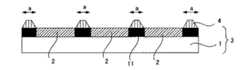
図3は、アクティブマトリックス方式の液晶表示装置パネルの一例である。液晶表示装置101は、カラーフィルタ11と液晶駆動側基板であるTFTアレイ基板12とを対向させて1〜10μm程度の間隙部13を設け、この間隙部13内に液晶Lを充填し、その周囲をシール材14で密封した構造をとっている(例えば特許文献1等)。カラーフィルタ11は、基材15上に、着色層17間の境界部を遮光するために所定のパターンに形成された遮光部16と、複数の色(通常、赤(R)、緑(G)、青(B)の3原色)を所定順序に配列した着色層17と、オーバーコート層18と、透明電極膜19とが、透明基板に近い側からこの順に積層された構造をとっている。 FIG. 3 shows an example of an active matrix liquid crystal display panel. In the liquid
一方、TFTアレイ基板12は、透明基板上にTFT素子を配列し、透明電極膜を設けた構造をとっている(図示せず)。また、カラーフィルタ11及びこれと対向するTFTアレイ基板12の内面側には配向膜20が設けられる。そして、着色層の背後にある液晶層の光透過率を制御することによってカラー画像が得られる。 On the other hand, the
ここで、間隙部13の厚さ、すなわちセルギャップ(カラーフィルタと液晶駆動側基板の間隙距離)は液晶層の厚さそのものであり、色ムラやコントラストムラといった表示ムラを防止し、均一な表示、高速応答性、高コントラスト比、広視野角等の良好な表示性能をカラー液晶表示装置に付与するためには、セルギャップを一定且つ均一に維持する必要がある。 Here, the thickness of the
セルギャップを維持する方法としては、例えば図3に示すように、間隙部13内にスペーサ部としてガラス、アルミナ又はプラスチック等からなる一定サイズの球状又は棒状粒子のビーズスペーサ部21を多数散在させ、カラーフィルタ11とTFTアレイ基板12とを貼り合わせ、液晶を注入する方法がある。この方法においては、ビーズスペーサ部の大きさをもってセルギャップが決定され、維持される。しかしながら、上記方法では、散布されたスペーサの密度に偏りが生じることがあり、この場合、カラーフィルタと液晶駆動側基板とのギャップを一定に保つことが難しいという問題があった。 As a method of maintaining the cell gap, for example, as shown in FIG. 3, a large number of spherical or rod-
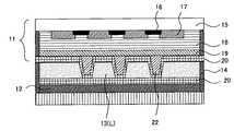
また、例えば図4に示すように、カラーフィルタ11の内面側であって遮光部16上(非表示領域)に、セルギャップに対応する高さを有する柱状スペーサ部22を形成する方法も一般的に行われている(例えば特許文献2等)。このような柱状スペーサ部22は、カラーフィルタの透明基板上に光硬化性樹脂を均一な厚みに塗布し、得られた塗膜をフォトリソグラフィーによってパターン露光して硬化させることにより、液晶表示装置の非表示領域に形成される。しかしながら、この方法においては、液晶表示装置が大面積化された場合等、柱状スペーサ部の高さを一定に形成することが難しく、液晶表示装置の表示ムラや表示不良が発生する場合がある、という問題があった。 For example, as shown in FIG. 4, a method of forming a
そこで、ビーズおよびバインダを含有するスペーサ部形成用塗工液を、インクジェット方式により、カラーフィルタ用基板上に塗布する方法も考えられている。しかしながらこの場合、スペーサ部の種類によっては、カラーフィルタ上に形成された配向膜をラビングする際や、カラーフィルタを洗浄する際に、スペーサ部が剥がれてしまったり、スペーサ部の高さを一定にすることが難しい等の問題があった。 Accordingly, a method of applying a spacer portion forming coating solution containing beads and a binder onto a color filter substrate by an ink jet method is also considered. However, in this case, depending on the type of the spacer portion, the spacer portion may be peeled off when the alignment film formed on the color filter is rubbed or the color filter is washed, or the height of the spacer portion may be constant. There were problems such as difficult to do.
そこで、液晶表示装置を形成する際等に、スペーサ部が剥がれてしまうこと等がなく、一定の高さでスペーサ部が形成されたカラーフィルタ、およびそのカラーフィルタを用いた液晶表示装置の提供が望まれている。 Therefore, when forming a liquid crystal display device, etc., there is provided a color filter in which the spacer portion is formed at a certain height without peeling off the spacer portion, and a liquid crystal display device using the color filter. It is desired.
本発明は、基材、および上記基材上にパターン状に複数形成された着色層を少なくとも有し、かつ表面が撥液化処理されたカラーフィルタ用基板と、上記カラーフィルタ用基板上に形成され、ビーズおよびバインダを含有するスペーサ部とを有するカラーフィルタであって、上記スペーサ部は、順テーパー形状とされていることを特徴とするカラーフィルタを提供する。 The present invention includes a base material, a color filter substrate having at least a plurality of colored layers formed in a pattern on the base material, and a liquid-repellent-treated surface, and the color filter substrate formed on the color filter substrate. A color filter having a spacer part containing beads and a binder, wherein the spacer part has a forward tapered shape.
本発明によれば、上記スペーサ部が順テーパー状とされていることから、カラーフィルタ用基板とスペーサ部とが接している面積が大きいものとすることができ、カラーフィルタ用基板とスペーサ部との密着性が高いものとすることができる。これにより、本発明のカラーフィルタ上に形成された配向膜をラビングする際や、上記カラーフィルタを洗浄する際等に、スペーサ部が剥がれてしまうことのないものとすることができる。また、上記スペーサ部が順テーパー状とされていることから、上記スペーサ部の頂部に存在するバインダの量を少ないものとすることができる。したがって、スペーサ部の高さをビーズの高さと同等とすることが可能となり、スペーサ部の高さにバラつきの少ないものとすることができるという利点も有している。 According to the present invention, since the spacer portion has a forward tapered shape, the area where the color filter substrate and the spacer portion are in contact with each other can be increased, and the color filter substrate and the spacer portion can be The adhesiveness can be high. Thereby, when the alignment film formed on the color filter of the present invention is rubbed or when the color filter is washed, the spacer portion can be prevented from peeling off. Further, since the spacer portion has a forward taper shape, the amount of the binder present at the top of the spacer portion can be reduced. Therefore, the height of the spacer portion can be made equal to the height of the beads, and there is an advantage that the height of the spacer portion can be less varied.
上記発明において、上記スペーサ部の上記バインダの表面は、上記ビーズの側面に位置する側面接触部から上記カラーフィルタ用基板表面側に徐々に傾斜するように形成されており、上記スペーサ部の外周側に位置する上記ビーズの上記側面接触部と上記カラーフィルタ用基板表面との間の距離のうち最も小さい距離が、上記ビーズの平均粒径の3/4〜1/2の範囲内であることが好ましい。これにより、上記スペーサ部とカラーフィルタ用基板との密着性を高いものとすることができる。またさらに、ビーズの頂部側に存在するバインダの量を少ないものとすることができることから、よりスペーサ部の高さにバラつきの少ないものとすることもできる。 In the above invention, the surface of the binder of the spacer portion is formed so as to be gradually inclined from the side surface contact portion located on the side surface of the bead to the color filter substrate surface side, and the outer peripheral side of the spacer portion The smallest distance among the distance between the side surface contact portion of the bead located at the surface and the color filter substrate surface is within a range of 3/4 to 1/2 of the average particle diameter of the bead. preferable. Thereby, the adhesiveness of the said spacer part and the board | substrate for color filters can be made high. Furthermore, since the amount of the binder existing on the top side of the bead can be reduced, the height of the spacer portion can be further reduced.
また上記発明においては、上記スペーサ部が、インクジェット法により形成されたものであることが好ましい。これにより、上記スペーサ部が高精細に効率よく形成されたものとすることができるからである。 Moreover, in the said invention, it is preferable that the said spacer part is formed by the inkjet method. This is because the spacer portion can be efficiently formed with high definition.
また本発明は、上述したカラーフィルタを有することを特徴とする液晶表示装置を提供する。本発明によれば、上記カラーフィルタが用いられていることから、カラーフィルタと液晶駆動側基板とのギャップを、上記スペーサ部により安定して一定に保つことが可能であり、表示ムラや表示不良等のない、高品質な液晶表示装置とすることができる。 The present invention also provides a liquid crystal display device having the color filter described above. According to the present invention, since the color filter is used, the gap between the color filter and the liquid crystal driving side substrate can be stably maintained constant by the spacer portion, and display unevenness and display failure can be achieved. Thus, a high-quality liquid crystal display device can be obtained.
本発明によれば、例えばカラーフィルタ上に形成された配向膜をラビングする際や、カラーフィルタを洗浄する際等に、スペーサ部が剥がれてしまうことのないものとすることができる。またさらに、目的とする高さに均一に、スペーサ部が形成されたものとすることができるという効果を奏するものである。 According to the present invention, for example, when the alignment film formed on the color filter is rubbed or when the color filter is washed, the spacer portion can be prevented from peeling off. Furthermore, there is an effect that the spacer portion can be formed uniformly at a target height.
本発明は、液晶表示装置に用いられる、ビーズを含有するスペーサ部を有するカラーフィルタ、およびそのカラーフィルタを用いた液晶表示装置に関するものである。以下、それぞれについてわけて説明する。 The present invention relates to a color filter having a spacer portion containing beads and a liquid crystal display device using the color filter, which is used in a liquid crystal display device. Each will be described separately below.
A.カラーフィルタ
まず、本発明のカラーフィルタについて説明する。本発明のカラーフィルタは、基材、および上記基材上にパターン状に複数形成された着色層を少なくとも有し、かつ表面が撥液化処理されたカラーフィルタ用基板と、上記カラーフィルタ用基板上に形成され、ビーズおよびバインダを含有するスペーサ部とを有するカラーフィルタであって、上記スペーサ部は、順テーパー形状とされていることを特徴とするものである。A. Color Filter First, the color filter of the present invention will be described. The color filter of the present invention includes a base material, a color filter substrate having at least a colored layer formed in a pattern on the base material, and a liquid-repellent-treated surface, and the color filter substrate. And a spacer part containing beads and a binder, wherein the spacer part has a forward taper shape.
本発明のカラーフィルタは、例えば図1に示すように、基材1、およびその基材1上にパターン状に形成された着色層2を少なくとも有するカラーフィルタ用基板3と、上記カラーフィルタ用基板3上に順テーパー状に形成されたスペーサ部4とを有するものである。また上記カラーフィルタ用基板3の表面は、撥液化処理されている。 As shown in FIG. 1, for example, the color filter of the present invention includes a substrate 1 and a
本発明によれば、上記スペーサ部が順テーパー状とされていることから、カラーフィルタ用基板とスペーサ部とが接している面積が大きいものとすることができる。したがって、カラーフィルタ用基板とスペーサ部との密着性が高いものとすることができ、本発明のカラーフィルタ上に形成された配向膜をラビングする際や、上記カラーフィルタを洗浄する際等に、スペーサ部が剥がれてしまうことのないものとすることができる。 According to the present invention, since the spacer portion has a forward tapered shape, the area where the color filter substrate and the spacer portion are in contact with each other can be increased. Therefore, the adhesion between the color filter substrate and the spacer portion can be high, when rubbing the alignment film formed on the color filter of the present invention, when washing the color filter, etc. The spacer portion can be prevented from peeling off.
また本発明においては、上記スペーサ部が順テーパー状とされていることから、上記スペーサ部の頂部に存在するバインダの量を少ないものとすることができる。したがって、スペーサ部の高さをビーズの高さとほぼ同等とすることができ、スペーサ部の高さにバラつきの少ないものとすることができるという利点も有している。
以下、本発明のカラーフィルタの各構成ごとに詳しく説明する。In the present invention, since the spacer portion has a forward tapered shape, the amount of the binder present at the top of the spacer portion can be reduced. Therefore, the height of the spacer portion can be made substantially equal to the height of the beads, and there is an advantage that the height of the spacer portion can be made less varied.
Hereinafter, each configuration of the color filter of the present invention will be described in detail.
1.スペーサ部
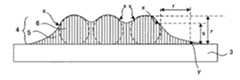
まず、本発明に用いられるスペーサ部について説明する。本発明に用いられるスペーサ部は、後述するカラーフィルタ用基板上に順テーパー状に形成されているものであり、ビーズおよびバインダを含有するものである。なお、上記スペーサ部が順テーパー形状であるとは、ビーズの基材への投影画像の面積よりもビーズとバインダからなるスペーサ部の基材への投影画像の面積が大きく、かつ、バインダと基材との接点がビーズの基材への投影画像の外側にあることをいう。1. Spacer part First, the spacer part used for this invention is demonstrated. The spacer portion used in the present invention is formed in a forward tapered shape on a color filter substrate described later, and contains beads and a binder. The spacer portion having a forward tapered shape means that the projected image area of the spacer portion made of beads and binder is larger than the area of the projected image of beads on the substrate, and the binder and base This means that the contact point with the material is outside the projected image of the beads on the substrate.
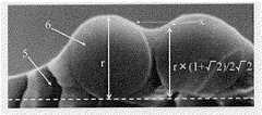
本発明においては、例えば図2に示すように、上記スペーサ部4の上記バインダ5の表面は、上記ビーズ6の側面に位置する側面接触部xからカラーフィルタ用基板3表面側に徐々に傾斜するように形成されており、上記スペーサ部4の外周側に位置する上記ビーズ6の上記側面接触部xとカラーフィルタ用基板3表面との間の距離のうち最も小さい距離sが、上記ビーズの平均粒径rの3/4〜1/2の範囲内、中でも5/8〜1/2の範囲内、特に3/5〜1/2の範囲内とされていることが好ましい。なお、上記側面接触部xとは、上記バインダ5の表面と上記ビーズ6の表面との距離、すなわちバインダ5の膜厚が100nmとなる部分をいうこととする。 In the present invention, for example, as shown in FIG. 2, the surface of the binder 5 of the
また、上記スペーサ部中に複数のビーズが含有されている場合であって、隣接するビーズとビーズとの距離が、ビーズの平均粒径の1/2以下である場合には、隣接するビーズ間に存在する上記側面接触部と、上記カラーフィルタ用基板との距離は、ビーズ平均粒径の(1+√2)/2√2〜1の範囲内、特に(1+√2)/2√2〜9/10の範囲内であることが好ましい。これにより、上記ビーズが近接している領域においても、スペーサ部とカラーフィルタ用基板との密着性が高いものとすることができるからである。 Further, in the case where a plurality of beads are contained in the spacer portion, and the distance between adjacent beads is equal to or less than ½ of the average particle diameter of the beads, the distance between adjacent beads The distance between the side surface contact portion present in the substrate and the color filter substrate is within the range of (1 + √2) / 2√2-1 of the average particle size of the beads, particularly (1 + √2) / 2√2 It is preferably within the range of 9/10. Thereby, even in the region where the beads are close to each other, the adhesion between the spacer portion and the color filter substrate can be made high.
また、本発明においては上記スペーサ部に含有される各ビーズの頂部近傍には、上記バインダが50nm以下、中でも25nm〜1nm程度、特に10nm〜1nm程度の膜厚で積層されていることが好ましい。これにより、上記スペーサ部の高さを上記ビーズの粒径とほぼ同等とすることができ、スペーサ部の高さにバラつきの少ないものとすることができるからである。 In the present invention, the binder is preferably laminated in the vicinity of the top of each bead contained in the spacer portion with a thickness of 50 nm or less, especially about 25 nm to 1 nm, particularly about 10 nm to 1 nm. This is because the height of the spacer portion can be made substantially equal to the particle size of the beads, and the height of the spacer portion can be reduced.
なお、上述したような形状の観察は、上記スペーサ部の断面を、例えば走査型電子顕微鏡により観察することにより行うことができる。 Note that the observation of the shape as described above can be performed by observing the cross section of the spacer portion with, for example, a scanning electron microscope.
また、上記ビーズの平均粒径とは、スペーサ部の形成に用いられるビーズの平均粒径を測定したものであり、隣接する10個のスペーサに含まれているビーズの粒径をそれぞれ走査型電子顕微鏡もしくは光学顕微鏡により拡大して測定し、それらビーズの粒径を算術平均した値である。 The average particle diameter of the beads is a measurement of the average particle diameter of the beads used for forming the spacer portion, and the particle diameters of the beads contained in the 10 adjacent spacers are respectively set as scanning type electrons. It is a value obtained by magnifying with a microscope or an optical microscope and arithmetically averaging the particle diameters of the beads.
ここで上記各スペーサ部に含有されるビーズの個数は、カラーフィルタの種類等によって適宜選択されるものであるが、通常、1個〜10個程度、中でも3個〜6個程度ビーズが含有されるものとされる。 Here, the number of beads contained in each of the spacer portions is appropriately selected depending on the type of the color filter and the like, but usually contains about 1 to 10 beads, especially about 3 to 6 beads. It is supposed to be.
また上記スペーサ部が形成される領域としては、上記着色層上であってもよいが、本発明においては特に、上記着色層どうしの境界領域上に形成されていることが好ましい。これにより、カラーフィルタが液晶表示装置に用いられた際、スペーサ部の存在によって着色層の透過率を低下させることがなく、輝度が高いものとすることができるからである。 The region where the spacer portion is formed may be on the colored layer, but in the present invention, it is particularly preferably formed on the boundary region between the colored layers. Thereby, when the color filter is used in the liquid crystal display device, the transmittance of the colored layer is not reduced by the presence of the spacer portion, and the luminance can be increased.
また上記スペーサ部の大きさや形状等としては、カラーフィルタの種類等に応じて適宜選択されることとなるが、本発明においては、個々のスペーサ部の断面積が500μm2〜8000μm2程度、中でも700μm2〜2800μm2程度、特に1250μm2〜1600μm2程度とされていることが好ましい。これにより、スペーサ部の存在によってカラーフィルタの輝度を低下させることの少ないものとすることができ、高輝度な液晶表示装置を形成可能なカラーフィルタとすることができるからである。As the size and shape of the spacer portion, but it becomes to be suitably selected according to the type of color filters and the like, in the present invention, the 500μm2 ~8000μm2 about the cross-sectional area of each spacer portion, among them 700μm2 ~2800μm2 mm, it is preferable that there is a particular 1250μm2 ~1600μm2 about. This is because it is possible to reduce the luminance of the color filter due to the presence of the spacer portion, and to provide a color filter capable of forming a high-luminance liquid crystal display device.
また本発明においては、1000μm角に形成されるスペーサ部の断面積の合計が2000μm2〜96000μm2程度、中でも5000μm2〜13000μm2程度となるように、個数が調整されてスペーサ部が形成されていることが好ましい。このような密度でスペーサ部が形成されているものとすることにより、本発明のカラーフィルタが液晶表示装置に用いられた際、カラーフィルタと液晶駆動側基板との間隙を一定に保つことが可能となるからである。In the present invention, total 2000μm2 ~96000μm2 about the cross-sectional area of the spacer portion formed 1000μm angle, so that inter alia 5000μm2 ~13000μm2 mm, the number is adjusted is formed spacer portion Preferably it is. By assuming that the spacer portion is formed with such a density, the gap between the color filter and the liquid crystal driving side substrate can be kept constant when the color filter of the present invention is used in a liquid crystal display device. Because it becomes.
また、上記スペーサ部の高さは、カラーフィルタの種類等により適宜選択されるが、通常1.0μm〜8μm程度、中でも2μm〜6μm程度とされることが好ましい。 The height of the spacer portion is appropriately selected depending on the type of color filter and the like, but is usually about 1.0 μm to 8 μm, and preferably about 2 μm to 6 μm.
また、上記バインダとしては、硬化性を有するものであって、本発明のカラーフィルタが液晶表示装置に用いられた際、カラーフィルタと液晶表示装置とのギャップを一定に保つことが可能なものであれば特に限定されるものではなく、例えば熱硬化性樹脂であってもよく、また光硬化性樹脂であってもよい。具体的には、アクリル系樹脂、エポキシ系樹脂、メラミン樹脂等が挙げられる。 The binder is curable and can maintain a constant gap between the color filter and the liquid crystal display device when the color filter of the present invention is used in the liquid crystal display device. There is no particular limitation as long as it is present, and it may be, for example, a thermosetting resin or a photocurable resin. Specific examples include acrylic resins, epoxy resins, melamine resins, and the like.
また、上記スペーサ部に用いられるビーズとしては、上記バインダと相溶性を有するものであれば、特に限定されるものではなく、一般的なカラーフィルタにビーズスペーサとして用いられるものと同様のものを用いることができる。例えば、ガラス、シリカ、金属酸化物(MgO、Al2O3)などの無機化合物の多孔質体や非多孔質体、中空体等や、ポリスチレン、ポリエチレン、ポリプロピレン、ポリエステル、ポリアクリル、ナイロン、シリコーン樹脂などのプラスチック類等を用いることができる。またこのようなビーズの表面は、上記バインダとの接着性を良好なものとするため、表面処理が施されたもの等であってもよい。In addition, the beads used in the spacer portion are not particularly limited as long as they are compatible with the binder, and the same beads as those used as a bead spacer in a general color filter are used. be able to. For example, porous, non-porous and hollow bodies of inorganic compounds such as glass, silica and metal oxides (MgO, Al2 O3 ), polystyrene, polyethylene, polypropylene, polyester, polyacryl, nylon, silicone Plastics such as resin can be used. In addition, the surface of such a bead may be subjected to surface treatment in order to improve the adhesiveness with the binder.
ここで上記ビーズの形状についても、特に限定されるものではなく、一般的なカラーフィルタにビーズスペーサとして用いられるものと同様の形状を有するものを用いることができるが、特にスペーサ部の高さの制御の面から球状であることが好ましい。またこの際、粒子径は1.0μm〜8.0μm程度、中でも2.5μm〜5.5μm程度であることが好ましい。これにより、スペーサ部の高さを上述したような範囲とすることができるからである。 Here, the shape of the beads is not particularly limited, and those having a shape similar to that used as a bead spacer in a general color filter can be used. Spherical shape is preferable from the viewpoint of control. At this time, the particle size is preferably about 1.0 μm to 8.0 μm, and more preferably about 2.5 μm to 5.5 μm. This is because the height of the spacer portion can be set in the above-described range.
また、本発明においては、上記スペーサ部の固形分中に75質量%〜95質量%程度、中でも85質量%〜90質量%程度、バインダが含有されていることが好ましい。これにより、上述したような形状に、スペーサ部を形成することが可能となるからである。 Moreover, in this invention, it is preferable that the binder contains about 75 mass%-about 95 mass%, especially about 85 mass%-about 90 mass% in solid content of the said spacer part. This is because the spacer portion can be formed in the shape as described above.
また、上記スペーサ部の形成方法としては、上述したバインダおよびビーズを、必要に応じて適宜添加剤や溶剤等と混合したスペーサ部形成用塗工液を、インクジェット法により塗布することにより形成することができる。なお、上記スペーサ部形成用塗工液に用いられる溶剤や、添加剤等としては、上記バインダの種類等に合わせて適宜選択され、一般的なインクジェット用インクに用いられるものと同様とすることができる。 In addition, as a method of forming the spacer part, the spacer part forming coating liquid, in which the above-described binder and beads are appropriately mixed with an additive, a solvent, or the like as necessary, is applied by an inkjet method. Can do. The solvent and additives used in the spacer portion-forming coating solution are appropriately selected according to the type of the binder and the like, and may be the same as those used for general inkjet inks. it can.
また、上記スペーサ部の形状を、上述したものとするためには、上記スペーサ部形成用塗工液をインクジェット法により、後述する表面が撥液化処理されたカラーフィルタ用基板上に、5pl〜20pl程度、中でも10pl〜15pl程度塗布し、乾燥・熱硬化させることが好ましい。 In addition, in order to make the shape of the spacer part as described above, the spacer part forming coating solution is formed on the color filter substrate whose surface, which will be described later, has been made liquid-repellent by an inkjet method, 5 pl to 20 pl. It is preferable to apply about 10 pl to 15 pl, and to dry and heat cure.
2.カラーフィルタ用基板
次に、本発明に用いられるカラーフィルタ用基板について説明する。本発明に用いられるカラーフィルタ用基板は、基材、および上記基材上にパターン状に、複数形成された着色層を少なくとも有し、かつ表面が撥液化処理されたものである。2. Next, the color filter substrate used in the present invention will be described. The substrate for color filter used in the present invention has at least a base material and a plurality of colored layers formed in a pattern on the base material, and the surface is subjected to a liquid repellency treatment.
本発明においては、上記基材および上記着色層を有するものであれば、その構成等は特に限定されるものではなく、例えば上記着色層どうしの境界領域に、上述したように遮光部が形成されているものであってもよく、また上記着色層上にオーバーコート層やITO層が形成されているものであってもよい。またさらに、本発明のカラーフィルタが、視野角度改善モードの一つである複数配向分割型垂直配向モード、すなわちMulti-domain Vertical Aligned(MVA)方式の液晶表示装置に用いられる場合等には、液晶配向制御用突起状部材等を有するものであってもよい。なお、上記カラーフィルタ用基板に用いられるオーバーコート層やITO層、液晶配向制御用突起状部材等については、一般的なカラーフィルタに用いられるものと同様とすることができるので、ここでの詳しい説明は省略する。
以下、上記カラーフィルタ用基板に用いられる着色層、基材、およびカラーフィルタ用基板表面の撥液化処理についてそれぞれ説明する。In the present invention, the configuration and the like are not particularly limited as long as the substrate and the colored layer are included. For example, the light shielding portion is formed in the boundary region between the colored layers as described above. The overcoat layer and the ITO layer may be formed on the colored layer. Furthermore, when the color filter of the present invention is used in a multi-alignment vertical alignment mode (ie, multi-domain vertical alignment (MVA) type liquid crystal display device), which is one of viewing angle improvement modes, It may have a projecting member for orientation control. The overcoat layer, the ITO layer, and the liquid crystal alignment control projection-like member used for the color filter substrate can be the same as those used for a general color filter. Description is omitted.
Hereinafter, the coloring layer used for the color filter substrate, the base material, and the liquid repellency treatment of the color filter substrate surface will be described.
(1)着色層
まず、本発明に用いられる着色層について説明する。本発明に用いられる着色層は、後述する基材上に、パターン状に、かつ複数形成されるものであれば特に限定されるものではない。隣り合う着色層と着色層との間には、間隙が設けられていてもよく、また隣接する着色層どうしが重なりあうように、形成されていてもよい。また上述したように、隣接する着色層どうしの間に、遮光部が設けられていてもよい。(1) Colored layer First, the colored layer used for this invention is demonstrated. The colored layer used in the present invention is not particularly limited as long as a plurality of colored layers are formed in a pattern on a substrate described later. A gap may be provided between the adjacent colored layers, or the adjacent colored layers may be formed so as to overlap each other. Further, as described above, a light shielding portion may be provided between the adjacent colored layers.
このような着色層は、通常、赤(R)、緑(G)、および青(B)の3色で形成される。また上記着色層における着色パターン形状は、ストライプ型、モザイク型、トライアングル型、4画素配置型等の公知の配列とすることができ、着色面積は任意に設定することができる。 Such a colored layer is usually formed of three colors of red (R), green (G), and blue (B). The colored pattern shape in the colored layer can be a known arrangement such as a stripe type, a mosaic type, a triangle type, a four-pixel arrangement type, and the colored area can be arbitrarily set.
ここで、本発明に用いられる着色層については、公知のカラーフィルタの着色層に用いられる材料や形成方法等により、形成することが可能であるので、ここでの詳しい説明は省略する。 Here, the colored layer used in the present invention can be formed by a material or a forming method used for a colored layer of a known color filter, and thus detailed description thereof is omitted here.
(2)基材
次に、本発明に用いられる基材について説明する。本発明に用いられる基材としては、通常カラーフィルタに用いられるものであれば特に限定されるものではなく、石英ガラス、パイレックス(登録商標)ガラス、合成石英板等の可撓性のない透明なリジッド材、あるいは、透明樹脂フィルム、光学用樹脂板等の可撓性を有する透明なフレキシブル材を用いることができる。(2) Substrate Next, the substrate used in the present invention will be described. The base material used in the present invention is not particularly limited as long as it is usually used for a color filter, and is not transparent such as quartz glass, Pyrex (registered trademark) glass, synthetic quartz plate. A rigid material or a transparent flexible material having flexibility such as a transparent resin film and an optical resin plate can be used.
(3)撥液化処理
次に、本発明におけるカラーフィルタ用基板表面の撥液化処理について説明する。本発明においては、カラーフィルタ用基板の表面が、表面張力が40mN/mの液体との接触角が、30°以上、中でも表面張力が40mN/mの液体との接触角が、50°以上とすることが好ましく、特に表面張力が40mN/mの液体との接触角が、70°以上となるように撥液化処理されていることが好ましい。これにより、上記スペーサ部を形成する際、スペーサ部形成用塗工液が濡れ広がってしまうことを防止することができ、上述したような形状に、均一な高さでスペーサ部が形成されたものとすることが可能となるからである。なお、上記液体との接触角は、上記表面張力を有する液体との接触角を接触角測定器(協和界面科学(株)製CA−Z型)を用いて測定(マイクロシリンジから液滴を滴下して30秒後)し、その結果から、もしくはその結果をグラフにして得られるものである。(3) Liquid Repellency Treatment Next, the liquid repellency treatment of the color filter substrate surface in the present invention will be described. In the present invention, the surface of the color filter substrate has a contact angle with a liquid having a surface tension of 40 mN / m of 30 ° or more, and particularly a contact angle with a liquid with a surface tension of 40 mN / m is 50 ° or more. In particular, the liquid repellent treatment is preferably performed so that the contact angle with a liquid having a surface tension of 40 mN / m is 70 ° or more. As a result, when the spacer portion is formed, the spacer portion forming coating liquid can be prevented from spreading and the spacer portion is formed at a uniform height in the shape as described above. This is because it becomes possible. The contact angle with the liquid is measured using a contact angle measuring device (CA-Z type, manufactured by Kyowa Interface Science Co., Ltd.) (dropping a droplet from a microsyringe). 30 seconds later), and the result can be obtained or graphed.
ここで本発明において、上記カラーフィルタ用基板の表面を撥液化処理する方法としては特に限定されるものではなく、カラーフィルタ用基板の種類等に応じて適宜選択することができる。例えば上記カラーフィルタ用基板表面に、撥液性を有する撥液層を形成する方法等であってもよく、また例えばカラーフィルタ用基板表面に、着色層やオーバーコート層等、有機材料からなる層が露出している場合には、これらの層にフッ素化合物を用いてプラズマ照射を行い、これらの層を撥液化する方法等であってもよい。 Here, in the present invention, the method for subjecting the surface of the color filter substrate to the liquid repellency treatment is not particularly limited, and can be appropriately selected according to the type of the color filter substrate. For example, a method of forming a liquid repellent layer having liquid repellency on the surface of the color filter substrate may be used. For example, a layer made of an organic material such as a colored layer or an overcoat layer on the surface of the color filter substrate. May be exposed to plasma using a fluorine compound for these layers to make these layers liquid repellent.
上記カラーフィルタ用基板上に、撥液層を形成することにより上記カラーフィルタ用基板表面を撥液化する方法として具体的には、撥液性の層を形成するために一般的に用いられるフッ化炭素からなる撥液層や、撥液性の有機基を有するシラン化合物を含有する撥液層等をカラーフィルタ用基板上に形成する方法等とすることができる。上記シラン化合物としては、例えばオルガノポリシロキサン等を挙げることができ、例えば特開2001−272774号公報等に記載されたものと同様のものを用いることができる。 Specifically, as a method of making the color filter substrate surface liquid repellent by forming a liquid repellent layer on the color filter substrate, a fluorination generally used for forming a liquid repellent layer is used. A liquid repellent layer made of carbon, a liquid repellent layer containing a silane compound having a liquid repellent organic group, or the like may be formed on the color filter substrate. Examples of the silane compound include organopolysiloxane and the like, and for example, those similar to those described in JP-A No. 2001-272774 can be used.
また上記撥液層が形成される領域としては、上記スペーサ部が形成される領域であれば、特に限定されるものではなく、例えばカラーフィルタ用基板全面に撥液層が形成されていてもよく、またカラーフィルタ用基板のうち一部のみに撥液層が形成されていてもよい。また上記撥液層の形成方法についても特に限定されるものではなく、例えばスピンコート法やダイコート法等の一般的な塗布方法であってもよく、またプラズマCVD法や熱CVD法等の化学気相蒸着法(CVD)法であってもよい。また例えば上記撥液層を形成するための撥液層形成用塗工液中に、上記カラーフィルタ用基板を浸漬等させて、カラーフィルタ用基板表面に撥液層を自己組織化させる方法等であってもよい。 The region where the liquid repellent layer is formed is not particularly limited as long as the spacer portion is formed. For example, the liquid repellent layer may be formed on the entire surface of the color filter substrate. In addition, a liquid repellent layer may be formed on only a part of the color filter substrate. Further, the method for forming the liquid repellent layer is not particularly limited, and may be a general coating method such as a spin coating method or a die coating method, or a chemical vapor deposition method such as a plasma CVD method or a thermal CVD method. A phase deposition method (CVD) method may be used. Further, for example, by immersing the color filter substrate in a liquid repellent layer forming coating liquid for forming the liquid repellent layer, the liquid repellent layer is self-organized on the surface of the color filter substrate. There may be.
なお、上記撥液層の膜厚としては、撥液層の種類等により適宜選択されるものであるが、通常0.001μm〜1.0μm程度、中でも0.001μm〜0.500μm、
特に0.001μm〜0.100μm程度とされることが好ましい。The film thickness of the liquid repellent layer is appropriately selected depending on the type of the liquid repellent layer and the like, but is usually about 0.001 μm to 1.0 μm, and more preferably 0.001 μm to 0.500 μm.
In particular, the thickness is preferably about 0.001 μm to 0.100 μm.
またカラーフィルタ用基板表面に有機材料からなる層が露出している場合に、プラズマを照射することによって、カラーフィルタ用基板表面を撥液化処理する方法として具体的には、フッ素化合物を導入ガスとして用い、カラーフィルタ用基板表面にプラズマを照射する方法とすることができる。これは、フッ素化合物を導入ガスとしてプラズマ照射をした場合、有機物にフッ素を導入することができることを利用したものである。上記プラズマ照射は、例えば真空中で行われるものであってもよく、また大気圧下で行われるものであってもよい。またプラズマ照射する領域としては、上記スペーサ部が形成される領域に少なくとも照射するものであれば特に限定されるものではなく、例えばカラーフィルタ用基板全面であってもよく、またカラーフィルタ用基板のうち一部の領域のみであってもよい。 In addition, when a layer made of an organic material is exposed on the surface of the color filter substrate, as a method of lyophobic treatment of the surface of the color filter substrate by irradiating plasma, specifically, a fluorine compound is used as an introduction gas. And a method of irradiating the surface of the color filter substrate with plasma. This utilizes the fact that fluorine can be introduced into an organic substance when plasma irradiation is performed using a fluorine compound as an introduction gas. The plasma irradiation may be performed in a vacuum, for example, or may be performed under atmospheric pressure. The region to be irradiated with plasma is not particularly limited as long as it irradiates at least the region where the spacer portion is formed. For example, the entire region of the color filter substrate may be used. Only some of the regions may be used.
上記プラズマを照射する際に用いられる導入ガスのフッ素化合物としては、例えばフッ化炭素(CF4)、窒化フッ素(NF3)、フッ化硫黄(SF6)、C2Cl3F3、C2F6、C3F6等が挙げられる。また、照射されるプラズマの照射条件としては、照射装置等により適宜選択されるものである。Examples of the fluorine compound of the introduced gas used when the plasma is irradiated include carbon fluoride (CF4 ), fluorine nitride (NF3 ), sulfur fluoride (SF6 ), C2 Cl3 F3 , and C2.F6,C 3 F6, and the like. Further, the irradiation conditions of the irradiated plasma are appropriately selected depending on the irradiation apparatus or the like.
ここで、本発明においては、上記プラズマ照射が大気圧下でのプラズマ照射であることが好ましい。これにより、減圧用の装置等が必要なく、コストや製造効率等の面から好ましいものとすることができるからである。このような大気圧プラズマの照射条件としては、以下のようなものとすることができる。例えば、電源出力としては、一般的な大気圧プラズマの照射装置に用いられるものと同様とすることができる。また、この際、照射されるプラズマの電極と、上記カラーフィルタ用基板表面との距離は、0.2mm〜20mm程度、中でも1mm〜5mm程度とされることが好ましい。またさらに、上記導入ガスとして用いられるフッ素化合物の流量は1L/min〜100L/min程度、中でも5L/min〜50L/min程度であることが好ましく、この際のカラーフィルタ用基板の搬送速度が0.1m/min〜10m/min程度、中でも0.5m/min〜5m/min程度が好ましい。 Here, in the present invention, the plasma irradiation is preferably plasma irradiation under atmospheric pressure. This is because an apparatus for decompression or the like is not necessary, which can be preferable in terms of cost, manufacturing efficiency and the like. The irradiation conditions of such atmospheric pressure plasma can be as follows. For example, the power output can be the same as that used in a general atmospheric pressure plasma irradiation apparatus. In this case, the distance between the irradiated plasma electrode and the color filter substrate surface is preferably about 0.2 mm to 20 mm, and more preferably about 1 mm to 5 mm. Furthermore, the flow rate of the fluorine compound used as the introduction gas is preferably about 1 L / min to 100 L / min, and more preferably about 5 L / min to 50 L / min. In this case, the conveyance speed of the color filter substrate is 0. .About.1 m / min to 10 m / min, especially about 0.5 m / min to 5 m / min is preferable.
なお上記カラーフィルタ用基板表面に導入されたフッ素の存在は、X線光電子分光分析装置(XPS:ESCALAB 220i-XL)による分析において、カラーフィルタ用基板の表面より検出される全元素中のフッ素元素の割合を測定することにより確認することができる。また、この際上記フッ素の割合としては、10%以上とされることが好ましい。 The presence of fluorine introduced on the surface of the color filter substrate is the elemental fluorine in all elements detected from the surface of the color filter substrate in the analysis by an X-ray photoelectron spectrometer (XPS: ESCALAB 220i-XL). This can be confirmed by measuring the ratio. At this time, the proportion of the fluorine is preferably 10% or more.
3.カラーフィルタ
次に、本発明のカラーフィルタについて説明する。本発明のカラーフィルタは、上記基材および着色層を有するカラーフィルタ用基板と、上記スペーサ部とを有するものであれば特に限定されるものではない。例えば上述したように、上記カラーフィルタ用基板に、遮光部やオーバーコート層、配向膜、液晶配向制御用突起状部材等が形成されているもの等であってもよい。3. Next, the color filter of the present invention will be described. The color filter of the present invention is not particularly limited as long as it has the color filter substrate having the base material and the colored layer and the spacer portion. For example, as described above, the color filter substrate may have a light shielding portion, an overcoat layer, an alignment film, a liquid crystal alignment control projection-shaped member, or the like.
B.液晶表示装置
次に、本発明の液晶表示装置について説明する。本発明の液晶表示装置は、上述したカラーフィルタを有するものである。本発明においては、上記カラーフィルタを有するものであれば、その構成は特に限定されるものではなく、一般的な液晶表示装置と同様とすることができる。具体的には、上記カラーフィルタと、対向して配置される液晶駆動側基板と、その対向基板との間に封入された液晶とを有するもの等とすることができる。B. Next, the liquid crystal display device of the present invention will be described. The liquid crystal display device of the present invention has the color filter described above. In the present invention, the configuration is not particularly limited as long as the color filter is included, and the configuration can be the same as that of a general liquid crystal display device. Specifically, the color filter, a liquid crystal driving side substrate disposed to face each other, and a liquid crystal sealed between the counter substrate and the like can be used.
本発明によれば、上記形状を有するスペーサ部を有するカラーフィルタが用いられていることから、液晶表示装置を製造する際、上記スペーサ部のビーズが剥がれてしまうこと等のないものとすることができる。また、上記スペーサ部は所定の高さとなるように均一に形成されていることから、本発明によれば、カラーフィルタと液晶駆動側基板とのギャップが一定に保たれた、表示ムラや表示不良等のない、高品質な液晶表示装置とすることができる。According to the present invention, since the color filter having the spacer portion having the above shape is used, the beads of the spacer portion are not peeled off when the liquid crystal display device is manufactured. it can. In addition, since the spacer portion is uniformly formed so as to have a predetermined height, according to the present invention, the gap between the color filter and the liquid crystal driving side substrate is kept constant, and display unevenness and display defects are maintained. Thus, a high-quality liquid crystal display device can be obtained.
なお、本発明に用いられる上記液晶層や液晶駆動側基板等については、一般的な液晶表示装置に用いられるものと同様とすることができるので、ここでの説明は省略する。 Note that the liquid crystal layer, the liquid crystal driving side substrate, and the like used in the present invention can be the same as those used in a general liquid crystal display device, and thus description thereof is omitted here.
また、本発明は上記実施形態に限定されるものではない。上記実施形態は、例示であり、本発明の特許請求の範囲に記載された技術的思想と実質的に同一な構成を有し、同様な作用効果を奏するものは、いかなるものであっても本発明の技術的範囲に包含される。 The present invention is not limited to the above embodiment. The above-described embodiment is an exemplification, and the present invention has substantially the same configuration as the technical idea described in the claims of the present invention, and any device that exhibits the same function and effect is the present invention. It is included in the technical scope of the invention.
<実施例1>
(カラーフィルタ用基板の準備)
ガラス基板からなる基材と、上記基材上にパターン状に形成されて遮光部と、上記遮光部により区画された開口部に形成された着色層と、上記遮光部及び着色層を覆うように形成された保護層とを有するカラーフィルタ用基板を準備した。
(撥液層形成用塗工液の準備)
下記材料を24時間常温にて攪拌し、加水分解共重合溶液を作製した。
・フルオロアルキルシラン(TSL8233 GE東芝シリコーン製)
:15.8wt%
・テトラメトキシシラン(TSL8114 GE東芝シリコーン製):52.8wt%
・0.1N塩酸 :31.6wt%
次に上記加水分解共重合溶液とイソプロピルアルコールと1,3ブタンジオールを重量比1:10:5で混合し、10分攪拌し、撥液層形成用塗工液とした。<Example 1>
(Preparation of color filter substrate)
A base material made of a glass substrate, a light shielding part formed in a pattern on the base material, a colored layer formed in an opening sectioned by the light shielding part, and the light shielding part and the colored layer so as to be covered A color filter substrate having a formed protective layer was prepared.
(Preparation of coating liquid for forming liquid repellent layer)
The following materials were stirred for 24 hours at room temperature to prepare a hydrolysis copolymer solution.
・ Fluoroalkylsilane (TSL8233 GE manufactured by Toshiba Silicone)
: 15.8 wt%
Tetramethoxysilane (TSL8114 GE manufactured by Toshiba Silicone): 52.8 wt%
・ 0.1N hydrochloric acid: 31.6wt%
Next, the hydrolysis copolymer solution, isopropyl alcohol, and 1,3 butanediol were mixed at a weight ratio of 1: 10: 5 and stirred for 10 minutes to obtain a liquid repellent layer forming coating solution.
(撥液層形成工程)
上記撥液層形成用塗工液を上述したカラーフィルタ用基板の保護層上にダイコート法により塗布し、150℃10分乾燥させた。これにより厚さ15nmの撥液層を得た。上記撥液層の表面張力が40mN/mの液体との接触角は70°であった。上記液体との接触角は接触角測定器(協和界面科学(株)製CA−Z型)によって測定した。(Liquid repellent layer forming step)
The liquid repellent layer forming coating solution was applied on the protective layer of the color filter substrate described above by a die coating method and dried at 150 ° C. for 10 minutes. As a result, a liquid repellent layer having a thickness of 15 nm was obtained. The contact angle of the liquid repellent layer with a liquid having a surface tension of 40 mN / m was 70 °. The contact angle with the liquid was measured with a contact angle measuring device (CA-Z type manufactured by Kyowa Interface Science Co., Ltd.).
(スペーサ部形成工程)
上記撥液層上に下記の組成を有するスペーサ部形成用塗工液を、1滴ずつ(15pl)、間隔510μmで塗布し、ホットプレートで80℃10分乾燥させ、その後オーブンにて230℃30分熱した。その結果直径40μmの円形状のドットが形成され、そのドットの中には平均5個のビーズが含有されたスペーサ部を得た。
[スペーサ部形成用塗工液]
熱硬化型樹脂:アクリル樹脂(主成分グリシジルメタクリレート):18.5wt%
希釈溶剤:ブチルカルビトールアセテート :80.0wt%
ビーズ:積水化学製ミクロパール 平均粒径4μm :1.5wt%(Spacer formation process)
On the liquid repellent layer, a spacer portion-forming coating solution having the following composition is applied drop by drop (15 pl) at an interval of 510 μm, dried on a hot plate at 80 ° C. for 10 minutes, and then in an oven at 230 ° C. 30 Divided heat. As a result, a circular dot having a diameter of 40 μm was formed, and a spacer portion containing an average of 5 beads in the dot was obtained.
[Spacer forming coating solution]
Thermosetting resin: Acrylic resin (main component glycidyl methacrylate): 18.5 wt%
Diluting solvent: Butyl carbitol acetate: 80.0 wt%
Beads: Micropearl made by Sekisui Chemical Average particle size 4μm: 1.5wt%
(評価)
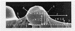
図5に示すスペーサ部の断面SEM画像から、スペーサ部の形状を評価した。スペーサ部のバインダ5の表面は、ビーズ6の側面に位置する側面接触部xからカラーフィルタ用基板表面側に徐々に傾斜するように形成されており、上記スペーサ部の外周側に位置する上記ビーズ6の上記側面接触部xとカラーフィルタ用基板表面との間の距離のうち最も小さい距離sが上記ビーズの平均粒径rの3/4〜1/2の範囲となった。
また、図6に示すスペーサ部の断面SEM画像から、隣接するビーズとビーズとの距離が、ビーズ平均粒径の1/2以下である場合についても評価を行ったところ、隣接するビーズ間に存在する側面接触部とカラーフィルタ用基板との距離は、ビーズ平均粒径rの(1+√2)/2√2〜1の範囲となった。ビーズを覆うバインダ5の形状が図5及び図6に示すような形状となることで、後工程でのブラシ洗浄にてビーズの剥離は皆無であった。(Evaluation)
From the cross-sectional SEM image of the spacer part shown in FIG. 5, the shape of the spacer part was evaluated. The surface of the binder 5 in the spacer portion is formed so as to be gradually inclined from the side contact portion x located on the side surface of the
In addition, from the cross-sectional SEM image of the spacer portion shown in FIG. 6, when the distance between the adjacent beads is 1/2 or less of the average bead particle size, the evaluation was made. The distance between the side surface contact portion and the color filter substrate was in the range of (1 + √2) / 2√2-1 of the average particle diameter r of beads. Since the shape of the binder 5 covering the beads is as shown in FIGS. 5 and 6, there was no peeling of the beads by brush cleaning in a subsequent process.
1 …基材
2 …着色層
3 …カラーフィルタ用基板
4 …スペーサ部
5 …バインダ
6 …ビーズDESCRIPTION OF SYMBOLS 1 ...
Claims (3)
Translated fromJapanese前記スペーサ部は、その固形分中に75質量%〜95質量%の範囲内で前記バインダが含有されており、
前記スペーサ部の前記バインダの表面は、前記ビーズの側面に位置する側面接触部から前記カラーフィルタ用基板表面側に徐々に傾斜するように形成されており、
前記スペーサ部の外周側に位置する前記ビーズの前記側面接触部と前記カラーフィルタ用基板表面との間の距離のうち最も小さい距離が、前記ビーズの平均粒径の3/4〜1/2の範囲内であり、
前記側面接触部から前記ビーズの平均粒径分、前記ビーズから離れた位置にバインダが存在し、その位置での前記バインダ表面とカラーフィルタ用基板表面との距離が、前記ビーズの平均粒径の1/4以下であることを特徴とするカラーフィルタ。A color filter substrate having at least a base material, and a plurality of colored layers formed in a pattern on the base material, the surface of which is subjected to a liquid repellency treatment; and a bead and a binder formed on the color filter substrate A color filter having a spacer portion containing
The spacer portion contains the binder in a range of 75% by mass to 95% by mass in its solid content,
The surface of the binder of the spacer portion is formed so as to be gradually inclined from the side surface contact portion located on the side surface of the bead to the color filter substrate surface side,
The smallest distance between the side surface contact portion of the bead located on the outer peripheral side of the spacer portion and the color filter substrate surface is 3/4 to 1/2 of the average particle diameter of the bead. Is in range,
A binder exists at a position away from the bead from the side surface contact portion by an average particle diameter of the bead, and the distance between the binder surface and the color filter substrate surface at the position is the average particle diameter of the bead. A color filter characterized by being1/4 or less .
Priority Applications (1)
| Application Number | Priority Date | Filing Date | Title |
|---|---|---|---|
| JP2005285488AJP5002936B2 (en) | 2005-09-29 | 2005-09-29 | Color filter and liquid crystal display device |
Applications Claiming Priority (1)
| Application Number | Priority Date | Filing Date | Title |
|---|---|---|---|
| JP2005285488AJP5002936B2 (en) | 2005-09-29 | 2005-09-29 | Color filter and liquid crystal display device |
Publications (2)
| Publication Number | Publication Date |
|---|---|
| JP2007094184A JP2007094184A (en) | 2007-04-12 |
| JP5002936B2true JP5002936B2 (en) | 2012-08-15 |
Family
ID=37979951
Family Applications (1)
| Application Number | Title | Priority Date | Filing Date |
|---|---|---|---|
| JP2005285488AExpired - Fee RelatedJP5002936B2 (en) | 2005-09-29 | 2005-09-29 | Color filter and liquid crystal display device |
Country Status (1)
| Country | Link |
|---|---|
| JP (1) | JP5002936B2 (en) |
Families Citing this family (4)
| Publication number | Priority date | Publication date | Assignee | Title |
|---|---|---|---|---|
| KR101319336B1 (en)* | 2007-09-28 | 2013-10-16 | 엘지디스플레이 주식회사 | Liquid crystl Display Device and Method for Manufacturing the Same |
| KR101308464B1 (en)* | 2007-10-01 | 2013-09-16 | 엘지디스플레이 주식회사 | Liquid Crystal Display Device and Method for Manufacturing the same |
| KR101286531B1 (en)* | 2007-10-02 | 2013-07-16 | 엘지디스플레이 주식회사 | Liquid Crystal Display Device and Method for Manufacturing the Same |
| KR101296653B1 (en)* | 2007-10-05 | 2013-08-14 | 엘지디스플레이 주식회사 | Liquid crystal Display Device and Method for Manufacturing the Same |
Family Cites Families (2)
| Publication number | Priority date | Publication date | Assignee | Title |
|---|---|---|---|---|
| JP3997038B2 (en)* | 1999-09-09 | 2007-10-24 | キヤノン株式会社 | Manufacturing method of color filter with spacer and liquid crystal element |
| JP4151377B2 (en)* | 2002-10-25 | 2008-09-17 | セイコーエプソン株式会社 | Electro-optical panel manufacturing method, electro-optical panel, and electro-optical device and electronic apparatus including the electro-optical panel |
- 2005
- 2005-09-29JPJP2005285488Apatent/JP5002936B2/ennot_activeExpired - Fee Related
Also Published As
| Publication number | Publication date |
|---|---|
| JP2007094184A (en) | 2007-04-12 |
Similar Documents
| Publication | Publication Date | Title |
|---|---|---|
| KR101609035B1 (en) | Method for producing color filter | |
| US20110269075A1 (en) | Method of fabricating color filter with flexible substrate | |
| TWI274193B (en) | Color filter and method for manufacturing the same, electro-optical device, and electronic apparatus | |
| JP4592448B2 (en) | Substrate for display device | |
| JP5002936B2 (en) | Color filter and liquid crystal display device | |
| JP2008225082A (en) | Color filter substrate and manufacturing method thereof | |
| JP4788203B2 (en) | Color filter and manufacturing method thereof | |
| US7288346B2 (en) | Color filter and production method thereof | |
| JP4788281B2 (en) | Color filter and liquid crystal display device | |
| JP4957057B2 (en) | Color filter and manufacturing method thereof | |
| JP5381605B2 (en) | Color filter manufacturing method and color filter | |
| JP5109248B2 (en) | Manufacturing method of color filter | |
| JP4342917B2 (en) | Manufacturing method of color filter | |
| JP2008225077A (en) | Color filter substrate and manufacturing method thereof | |
| JP2008298887A (en) | Color filter and liquid crystal display device | |
| JP2007139939A (en) | Manufacturing method of color filter | |
| JP2007065582A (en) | Color filter and manufacturing method thereof | |
| JP2007219482A (en) | Manufacturing method of color filter | |
| JP2007094185A (en) | Color filter and liquid crystal display device | |
| JP4779772B2 (en) | Color filter and liquid crystal display device using the same | |
| JP2007272148A (en) | Color filter and liquid crystal display device using the same | |
| JP4752337B2 (en) | Manufacturing method of color filter | |
| JP2007272181A (en) | Manufacturing method of color filter | |
| JP2004325736A (en) | Color filter, method of manufacturing the same, and liquid crystal element using color filter | |
| JP5771931B2 (en) | Color filter, liquid crystal display device using the same, and method of manufacturing color filter |
Legal Events
| Date | Code | Title | Description |
|---|---|---|---|
| A621 | Written request for application examination | Free format text:JAPANESE INTERMEDIATE CODE: A621 Effective date:20080819 | |
| A131 | Notification of reasons for refusal | Free format text:JAPANESE INTERMEDIATE CODE: A131 Effective date:20110426 | |
| A977 | Report on retrieval | Free format text:JAPANESE INTERMEDIATE CODE: A971007 Effective date:20110427 | |
| A521 | Written amendment | Free format text:JAPANESE INTERMEDIATE CODE: A523 Effective date:20110627 | |
| A131 | Notification of reasons for refusal | Free format text:JAPANESE INTERMEDIATE CODE: A131 Effective date:20120214 | |
| A521 | Written amendment | Free format text:JAPANESE INTERMEDIATE CODE: A523 Effective date:20120404 | |
| TRDD | Decision of grant or rejection written | ||
| A01 | Written decision to grant a patent or to grant a registration (utility model) | Free format text:JAPANESE INTERMEDIATE CODE: A01 Effective date:20120424 | |
| A01 | Written decision to grant a patent or to grant a registration (utility model) | Free format text:JAPANESE INTERMEDIATE CODE: A01 | |
| A61 | First payment of annual fees (during grant procedure) | Free format text:JAPANESE INTERMEDIATE CODE: A61 Effective date:20120507 | |
| FPAY | Renewal fee payment (event date is renewal date of database) | Free format text:PAYMENT UNTIL: 20150601 Year of fee payment:3 | |
| R150 | Certificate of patent or registration of utility model | Free format text:JAPANESE INTERMEDIATE CODE: R150 | |
| LAPS | Cancellation because of no payment of annual fees |