JP4996929B2 - Virtual computer system - Google Patents
Virtual computer systemDownload PDFInfo
- Publication number
- JP4996929B2 JP4996929B2JP2007008220AJP2007008220AJP4996929B2JP 4996929 B2JP4996929 B2JP 4996929B2JP 2007008220 AJP2007008220 AJP 2007008220AJP 2007008220 AJP2007008220 AJP 2007008220AJP 4996929 B2JP4996929 B2JP 4996929B2
- Authority
- JP
- Japan
- Prior art keywords
- dma
- virtual
- virtual server
- request
- priority
- Prior art date
- Legal status (The legal status is an assumption and is not a legal conclusion. Google has not performed a legal analysis and makes no representation as to the accuracy of the status listed.)
- Expired - Fee Related
Links
Images


Classifications
- G—PHYSICS
- G06—COMPUTING OR CALCULATING; COUNTING
- G06F—ELECTRIC DIGITAL DATA PROCESSING
- G06F13/00—Interconnection of, or transfer of information or other signals between, memories, input/output devices or central processing units
- G06F13/14—Handling requests for interconnection or transfer
- G06F13/20—Handling requests for interconnection or transfer for access to input/output bus
- G06F13/28—Handling requests for interconnection or transfer for access to input/output bus using burst mode transfer, e.g. direct memory access DMA, cycle steal
- G—PHYSICS
- G06—COMPUTING OR CALCULATING; COUNTING
- G06F—ELECTRIC DIGITAL DATA PROCESSING
- G06F13/00—Interconnection of, or transfer of information or other signals between, memories, input/output devices or central processing units
- G06F13/14—Handling requests for interconnection or transfer
- G06F13/36—Handling requests for interconnection or transfer for access to common bus or bus system
Landscapes
- Engineering & Computer Science (AREA)
- Theoretical Computer Science (AREA)
- Physics & Mathematics (AREA)
- General Engineering & Computer Science (AREA)
- General Physics & Mathematics (AREA)
- Bus Control (AREA)
Description
Translated fromJapanese本発明は、仮想計算機システムに関し、複数の仮想サーバでIO(Input/Output)デバイスを共有させる技術に関する。 The present invention relates to a virtual computer system, and relates to a technique for sharing an IO (Input / Output) device among a plurality of virtual servers.
1つの計算機上で複数の仮想的なサーバを構成し、各サーバで個別にOS(Operating System)を稼動させる仮想計算機システムが広く知られている。仮想計算機システムで、多数の仮想サーバを稼動させるためには、IOデバイスを仮想サーバ間で共有させる必要がある。 A virtual computer system in which a plurality of virtual servers are configured on one computer and an OS (Operating System) is individually operated on each server is widely known. In order to operate a large number of virtual servers in a virtual computer system, it is necessary to share IO devices between the virtual servers.
仮想サーバ間でIOデバイスを共有させる技術として、ソフトウェアによりIOデバイスをエミュレーションさせる方法が知られている。特許文献1で開示された方法では、仮想サーバ上のOSに対して仮想IOデバイスを提供する。仮想マシンモニタ(Virtual Machine Monitor、以下、VMM)は、仮想IOデバイスへのアクセスを受信してホストOSに転送し、ホストOSが物理的なIOデバイスへのアクセスを一元的に管理する。 As a technique for sharing an IO device between virtual servers, a method of emulating an IO device by software is known. In the method disclosed in
また、仮想サーバ間でIOデバイスを共有させる他の技術として、IOデバイスへのアクセスを仮想サーバ間で調停する調停ハードウェアを使用する方法が知られている。特許文献2で開示された方法では、メモリマップトIO(MMIO)レジスタへの書込みを監視し、特定のレジスタへの書込みを契機に、物理的なIOデバイスへのアクセスを実施する。 As another technique for sharing an IO device between virtual servers, a method using arbitration hardware for arbitrating access to an IO device between virtual servers is known. In the method disclosed in
しかしながら、特許文献1記載の従来例では仮想サーバ間でのIOアクセスについて、優先度やQoS(Quality of Service)保証を考慮した制御は実施されておらず、仮想サーバ上で稼動させるサービスの優先度に応じて、IO帯域を指定することは実現できなかった。 However, in the conventional example described in
また、仮にVMM等のソフトウェア要素でIOアクセスに一定の制限を持たせた場合、IO処理に関する性能オーバヘッドが増大するため、将来的なIOデバイスの広帯域化を見越した場合に十分と言えない。 Also, if a certain restriction is imposed on IO access by software elements such as VMM, the performance overhead related to IO processing increases, so it cannot be said to be sufficient in anticipation of future broadbandization of IO devices.
一方、特許文献2記載の従来例では、複数の仮想サーバが同時に調停ハードウェアへアクセスするため、仮想サーバのIO優先順位に応じて調停を行うことは実現されていない。 On the other hand, in the conventional example described in
そこで本発明は上記の問題点に鑑み、仮想サーバ間でのIO共有時の性能オーバヘッドを抑えつつ、かつ仮想サーバの優先度に応じたIOアクセスの調停と帯域制御を実現した計算機システムを提供することを目的とする。 Therefore, in view of the above problems, the present invention provides a computer system that realizes IO access arbitration and bandwidth control according to the priority of a virtual server while suppressing performance overhead when sharing IO between virtual servers. For the purpose.
本発明は、中央処理部(Central Processing Unit、以下CPU)とメモリとIOインタフェースを有する計算機であって、この計算機を、複数の仮想サーバを生成するハイパバイザと、IOインタフェースを制御するIOコントローラを有し、このIOコントローラは、IOインタフェースからDMA(Direct Memory Access)要求を受信するDMA受信部と、受信したDMA要求をデコードし対応する仮想サーバを特定する第1のデコーダと、仮想サーバ別にDMA処理状況を監視するDMA監視カウンタと、仮想サーバ別に予め設定された閾値レジスタと、DMA監視カウンタと閾値レジスタの値を比較し、受信したDMA要求の処理の優先度を決定する優先度決定回路を有する構成とする。 The present invention is a computer having a central processing unit (CPU), a memory, and an IO interface. The computer includes a hypervisor that generates a plurality of virtual servers and an IO controller that controls the IO interface. This IO controller includes a DMA receiver that receives a DMA (Direct Memory Access) request from the IO interface, a first decoder that decodes the received DMA request and identifies the corresponding virtual server, and a DMA process for each virtual server. A DMA monitoring counter that monitors the situation, a threshold register that is preset for each virtual server, and a priority determination circuit that compares the values of the DMA monitoring counter and the threshold register to determine the priority of processing of the received DMA request The configuration.
また、CPUとメモリとIOデバイスを有する計算機において、該計算機は、複数の仮想サーバを生成するハイパバイザを有し、前記IOデバイスは、DMA要求を発行するDMA要求発行部と、仮想サーバ別にDMA発行状況を監視するDMA監視カウンタと、仮想サーバ別に予め設定された閾値レジスタと、前記DMA監視カウンタと閾値レジスタの値を比較し、発行するDMA要求の優先順位を決定する優先度決定回路を有する。 Further, in a computer having a CPU, a memory, and an IO device, the computer has a hypervisor that generates a plurality of virtual servers, and the IO device issues a DMA request issuing unit that issues a DMA request, and a DMA issue for each virtual server. A DMA monitoring counter for monitoring the situation, a threshold register preset for each virtual server, and a priority determination circuit for comparing the DMA monitoring counter and the value of the threshold register to determine the priority of the DMA request to be issued.
本発明の構成では、IOコントローラもしくはIOデバイスが仮想サーバ別にDMAの処理状況もしくは発行状況を閾値と比較して監視する。これによりVMM等のソフトウェアに依存しないためIO共有時の性能オーバヘッドを抑えつつ、かつ仮想サーバの優先度に応じたIOアクセスの調停と帯域制御の実現を可能とする。 In the configuration of the present invention, the IO controller or IO device monitors the DMA processing status or issuance status for each virtual server by comparing it with a threshold value. As a result, since it does not depend on software such as VMM, performance overhead when sharing IO is suppressed, and arbitration of IO access and bandwidth control according to the priority of the virtual server can be realized.
以下、本発明の実施形態を添付図面に基づいて説明する。 Hereinafter, embodiments of the present invention will be described with reference to the accompanying drawings.
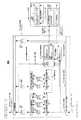
図1は、第一の実施例を含めた各実施例が想定する仮想計算機システムの一構成例を示す。計算機は、大別してハードウェア構成要素1001と、ソフトウェア構成要素1002から構成される。 FIG. 1 shows a configuration example of a virtual machine system assumed by each embodiment including the first embodiment. The computer is roughly composed of a
ハードウェア構成要素1001には、処理部であるCPU1003aおよび1003bと、記憶部であるメモリ1004、IOデバイス1005が含まれ、それぞれがチップセット1006を介して相互に接続されている。チップセット1006に対して、CPU1003aおよび1003bはCPUバス1010を、メモリ1004はメモリインタフェース1011を、IOデバイス1005はIOインタフェース1012および拡張IOスロット1013を、それぞれ介して接続される。IOデバイス1005には更にHDD (Hard Disk Drive) 1014もしくはネットワーク1015が接続される。 The
チップセット1006は、内部的にCPUバスコントローラ1007、メモリコントローラ1008、IOコントローラ1009に区分され、それぞれ接続されたCPUバス1010、メモリインタフェース1011、IOインタフェース1012の制御を担う。なお、図面の都合上、ハードウェア構成要素1001の各要素の個数を1つもしくは2つとして図示したが、特にそれらに限定するものではない。またIOインタフェース1012として、業界標準のPCI expressリンクを主に想定しているが、特にこれらに限らず他のIOバスやIOポートにも適用可能である。 The
ソフトウェア構成要素1002には、ハイパバイザ1020、および仮想サーバ1021aと1021bが含まれる。ハイパバイザ1020は、仮想サーバ1021aおよび1021bの生成および制御を行うと共に、管理用端末1024へ接続され、サーバ管理者1025からの操作を受け付ける。サーバ管理者1025は、仮想サーバの生成や仮想サーバへのハードウェア構成要素1001の割当等を指示する。仮想サーバ1021aでは、ゲストOS1022が1つ、およびゲストアプリケーション1023が1つ以上稼動する。なお、図面の都合上、仮想サーバ1021aと1021bを2つのみの例を示したが、特に上記に限定するものではなく、3つ以上もしくは1つ以下でも構わない。 The
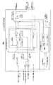
図2は、図1のチップセット1006の内部構成を示し、特にIOコントローラ1009周辺を詳細化して示した図である。IOコントローラ1009は、CPUバスコントローラ1007およびメモリコントローラ1008と、IO to CPU/メモリ通信インタフェース1104 および CPU/メモリ to IO通信インタフェース1105を介して接続される。 FIG. 2 shows the internal configuration of the chip set 1006 of FIG. 1, and particularly shows the
IOコントローラ1009は、内部的にInbound(受信側)制御サブユニット1101と、Outbound(送信側)制御サブユニット1102の2つに大別され、IOインタフェース1012に対して、IOインタフェースアービタ1103を介して接続される。 The
Inbound制御サブユニット1101は、IOインタフェース1012からのトランザクション(Transaction、以下Txと略す)を受信し、IO to CPU/メモリ通信インタフェース1104へ転送する役割を担う。以下に説明する本発明の各実施例では、Inbound制御サブユニット1101は、更にハイパバイザ1020と対ハイパバイザ通信インタフェース1106を介して通信する機能を有する。なお、対ハイパバイザ通信インタフェース1106の実現方法としては、MMIOレジスタやIOレジスタ、割込み、メモリ上のデータ構造、およびそれらの組合せなど複数のインプリメンテーションが考えられる。これらの実現方法自身は、いずれもハードウェア設計者やハイパバイザ設計者にとって容易に想像できる範囲の技術であるため、ここでは詳述しない。Outbound制御サブユニット1102は、CPU/メモリ to IO通信インタフェース1105からのTxを受信し、IOインタフェース1012へ転送する役割を担う。 The
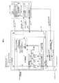
図3は、実施例1の主要部の構成を示しており、Inbound制御サブユニット1101およびソフトウェア構成要素1002の内部構成について開示している。前述の対ハイパバイザ通信インタフェース1106は、内部的に流量オーバ通信インタフェース1355およびレジスタ操作インタフェース1356の2インタフェースから構成されており、Inbound制御サブユニット1101とハイパバイザ1020間を接続する。なお、流量オーバ通信インタフェース1355からは、流量オーバを生じた仮想サーバ情報などが送信される。 FIG. 3 shows the configuration of the main part of the first embodiment, and discloses the internal configuration of the
Inbound制御サブユニット1101は、IOインタフェースアービタ1103からのTxをTLP(Transaction Layer Packet)デコーダ&MUX1301で受信する。DMA要求を受信するDMA受信部であるTLPデコーダ&MUX1301は、PCI express規約に則り受信したTxを、Posted要求1302、Non-Posted要求1303、Completion要求1304の3つに分類する。本実施例で解決を意図しているIOアクセスの帯域制御に関して、大部分を占めるTxはDMAライト要求、およびDMAリード要求であると考えられる。そこで、DMAライト要求が含まれるPosted要求1302、およびDMAリード要求が含まれるNon-Posted要求1303について、仮想サーバの優先度に応じた調停処理を実施する方針とする。 The
Posted要求1302は、Posted優先度決定回路1305を経由して、HQ(Higher- prioritized Queue)1307a、LQ(Lower-prioritized Queue)1308a、SoQ(Strong-ordered Queue)1309のいずれかに格納される。各キューは、HQ1307a > LQ1308a > SoQ1309の順に高い処理優先度を有する。 Posted
一方、Non-Posted要求1303は、Non-Posted優先度決定回路1306を経由して、HQ1307bもしくはLQ1308bのいずれかに格納される。各キューは、HQ1307b > LQ1308bの順に高い処理優先度を有する。 On the other hand, the Non-Posted
優先度決定部として機能する優先度決定回路1305および1306は、いずれもDMA流量監視回路1317が生成する処理優先度1323の値に応じて、受信した要求の格納先を決定する。本実施例において、処理優先度1323の値は、0のとき受信した要求に対して低い優先度を設定し、1のとき高い優先度を設定することを意味する。 Each of the
DMA流量監視回路1317は、Posted要求1302およびNon-Posted要求1303の各要求およびVM情報デコーダ1321が生成する仮想サーバ番号(以下、VM番号あるいはVM#)1322、およびレジスタ操作インタフェース1356でハイパバイザから設定された情報に従って、処理優先度1323を決定する。 The DMA flow rate monitoring circuit 1317 is set from the hypervisor by each request of the posted
VM情報デコーダ1321は、Posted要求1302およびNon-Posted要求1303の要求Txのヘッダおよびレジスタ操作インタフェース1356で設定された値を参照して、これらの要求に対応する仮想サーバを特定し、VM番号1322を出力する。この仮想サーバ特定部として機能するVM情報デコーダ1321の実現方法は複数考えられるが、例えば要求のヘッダ中のアドレスビットの一部をVM番号と見做す方法や、アドレス範囲毎に対応するVM番号を保持しておきTx受信毎にこれをチェックする方法などが考えられる。 The
DMA流量監視回路1317についてはいくつかの実現例が考えられるが、2つの実施例を図4および図6を用いて説明する。 Several implementation examples of the DMA flow rate monitoring circuit 1317 are conceivable. Two embodiments will be described with reference to FIGS. 4 and 6. FIG.
図4に、DMA流量監視回路1317の実施例1を示す。本実施例では、DMA流量監視回路1317はDMA監視カウンタ1319を有し、内部的に後いくつの要求が受信可能かを示すクレジット情報1405a、1405bを仮想サーバ別に保持している。なお、クレジット情報1405aとクレジット情報1405bの各情報(ラッチ)および周辺の設定回路については同一であるため、クレジット情報1405aについてのみ詳細を記載している。 FIG. 4 shows a first embodiment of the DMA flow rate monitoring circuit 1317. In this embodiment, the DMA flow rate monitoring circuit 1317 has a
本クレジット情報は、レジスタ操作インタフェース1356から派生するクレジット設定CMD1402およびクレジット設定値1401を介してハイパバイザ1020から設定される。 This credit information is set from the
上記クレジット情報は、Posted要求1302およびNon-Posted要求1303の各要求の受信時にデクリメントされ、各要求の処理が完了したことを示すTx完了情報1316のアサートを契機にインクリメントされる。上記デクリメントおよびインクリメント時に操作されるクレジット情報は一時に1つのみで、VM番号1322によって特定される仮想サーバに対応する情報が選択的に操作される。 The credit information is decremented upon receipt of each of the posted
クレジット設定CMD1402によるクレジット情報設定、および上記デクリメント、インクリメント操作が実施されない場合、クレジット情報設定SEL1407が defaultのデータを選択し、前クレジット情報が維持される。本クレジット情報は、いずれもレジスタ操作インタフェース1356を介してハイパバイザ1020から読み出し可能である。 When the credit information setting by the credit setting CMD1402 and the decrementing and incrementing operations are not performed, the credit information setting SEL1407 selects default data, and the previous credit information is maintained. The credit information can be read from the
DMA流量監視回路1317は、仮想サーバ毎に優先的に処理可能なDMA数の情報を、閾値レジスタ1320中の閾値レジスタ値1406aおよび1406bに保持する。閾値レジスタ値1406aおよび1406bは仮想サーバ別に設けられ、レジスタ操作インタフェース1356から派生する閾値設定CMD1404および閾値設定値1403を介してハイパバイザから設定される。図面では、1406aに閾値 “4”が、1406bに閾値 “6”がそれぞれ設定された例を示している。 The DMA flow rate monitoring circuit 1317 holds information on the number of DMAs that can be preferentially processed for each virtual server in the threshold register values 1406a and 1406b in the
DMA流量監視回路1317は比較器1318を有し、クレジット情報と閾値レジスタ値を比較する。比較対象のクレジット情報および閾値レジスタ値はVM番号1322によって指定され、クレジット情報選択SEL1408および閾値レジスタ選択SEL1409が比較対象を選択する。 The DMA flow rate monitoring circuit 1317 has a comparator 1318 and compares the credit information with the threshold value register value. The credit information and threshold register value to be compared are specified by the
比較器1318では、クレジット情報が閾値レジスタ値よりも小さい場合に、対応する仮想サーバに設定されたIO帯域を超過したと判断する。その理由は、受信して処理中のDMA処理数が増加して想定値を超えてしまい、クレジットが想定よりも小さくなったと考えられるからである。本ケースでは処理優先度1323に1がアサートされ、受信した要求が低い優先度のキューに格納される。またこの所定の優先度として低い優先度が選択されたと同時に、流量オーバ通知インタフェース1355もアサートされ、ハイパバイザ1020に対して何れかの仮想サーバがIO帯域を超過したことを通知する。なお、図4の回路構成においては、アサートされる流量オーバ通知インタフェース1355のみが図示されているが、先に述べたように、アサートと同時にインタフェース1355を介して、対応する仮想サーバの仮想サーバ番号(VM番号1322)がハイパバイザ1020に送信される。なお、この実現方法は、ハードウェア設計者にとって容易に構成できる範囲の技術であるため、ここでは詳述しない。 When the credit information is smaller than the threshold register value, the comparator 1318 determines that the IO bandwidth set for the corresponding virtual server has been exceeded. The reason is that it is considered that the number of DMA processes being received and processed increases to exceed the assumed value, and the credit is smaller than expected. In this case, 1 is asserted to the
一方、比較器1318で、クレジット情報が閾値レジスタ値以上の値を保っている場合、対応する仮想サーバに設定されたIO帯域を超過していないと判断する。本ケースでは1323処理優先度に0が出力され、受信した要求が高い優先度のキューに格納される。 On the other hand, the comparator 1318 determines that the IO bandwidth set in the corresponding virtual server has not been exceeded when the credit information is maintained at a value equal to or greater than the threshold register value. In this case, 0 is output as the 1323 processing priority, and the received request is stored in the high priority queue.
図6に、DMA流量監視回路の実施例2を示す。本実施例では、DMA監視カウンタ1319がデータペイロード長カウンタ1604a、1604bを有し、仮想サーバ別に処理済みのDMAも含めて受信済みの要求のデータペイロード長の累算値を保持する。 FIG. 6 shows a second embodiment of the DMA flow rate monitoring circuit. In this embodiment, the
データペイロード長カウンタ1604a、1604bは、リセット信号1601を介してハイパバイザ1020からリセット可能である。ハイパバイザ1020の構成は図7に後述するが、定期的に本カウンタをリセットして、単位時間当たりに受信されたDMA要求量を監視可能とする。 The data payload length counters 1604a and 1604b can be reset from the
上記データペイロード長カウンタ1604a、1604bは、要求1302、1303の受信時にカウントアップされる。加算される値は、要求1302、1303のTxヘッダに含まれるデータペイロード長であり、デコーダ1607によって特定される。要求1302および1303の要求アサート時に、VM番号1322に対応して加算CMD1603がアサートされ、データペイロード長カウンタ1604aもしくは1604bが加算される。加算CMD1603がアサートされない場合は、前情報が維持される。 The data payload length counters 1604a and 1604b are counted up when the
図6の実施例では、閾値レジスタ値1406cおよび1406dに、優先的に処理可能なDMAペイロード長の累算値をDW(Double Word: 4byte)単位で保持する。図6では、閾値レジスタ1406cに 1,024、および閾値レジスタ1406dに 2,048が格納されており、それぞれ単位時間当たりに1,024DW(4KB)および2,048DW(8KB)までのDMA要求を優先的に処理可能であることを示している。 In the embodiment of FIG. 6, the
比較器1318bでは、データペイロード長カウンタの値が閾値レジスタ値よりも大きい場合に、対応する仮想サーバに設定されたIO帯域を超過したと判断する。上記以外の場合、IO帯域を超過していないと判断する。なお、処理優先度1323および流量オーバ通知インタフェース1355のアサートについては、図4に示した実施例1と同一とする。 When the value of the data payload length counter is larger than the threshold register value, the
図4および図6を用いたDMA流量監視回路の実施例の説明は以上である。いずれの方法を用いても仮想サーバごとに設定された閾値に応じてIO帯域の大部分を占めるDMAの流量を監視できることを示した。なお、DMA流量監視回路については、閾値のデータを増やして複数レベルの優先度を出力する、データクレジット情報を用いてDMA流量を判断する、データペイロード長カウンタをDMA流量監視回路1317内のみで定期的にリセットする、などの変形例が考えられる。しかし、いずれも回路設計者およびハイパバイザ設計者ならば、上述した実施例の記載から容易に類推可能であり、ここでは説明を省略する。 This is the end of the description of the embodiment of the DMA flow rate monitoring circuit using FIG. 4 and FIG. It was shown that the flow rate of DMA occupying most of the IO bandwidth can be monitored according to the threshold set for each virtual server using either method. As for the DMA flow rate monitoring circuit, the threshold data is increased and multiple levels of priority are output, the data flow information is judged using the data credit information, and the data payload length counter is periodically set only within the DMA flow rate monitoring circuit 1317. It is possible to consider a modification such as resetting automatically. However, any circuit designer and hypervisor designer can easily infer from the description of the above-described embodiment, and the description is omitted here.
次に、図5を用いて図3の優先度決定部であるPosted/Non-Posted優先度決定回路1305、1306の実施例を示す。Posted要求1302は、要求の種類および処理優先度1323に応じて3段階の優先度をつけられ、それぞれ異なるキューにエンキューされる。本優先度の決定をPosted優先度決定回路1305が行う。 Next, an embodiment of Posted / Non-Posted
Posted優先度決定回路1305では、受信した要求をAttributeデコーダ1501がデコードし、Strong Ordered属性が指定されているか否か判定する。PCI express規約規定では、Strong Ordered指定されたPosted要求は、先行する如何なるPosted要求も追い越してはならないと定められている。そこで、Strong Ordered指定されたPosted要求を受信した場合Strong Ordered信号1502がアサートされる。本信号により処理優先度1323に関わらずPosted SoQエンキュー信号1326がアサートされ、受信したPosted要求1302は後段のSoQ1309へエンキューされる。 In the Posted
Strong Ordered信号1502がアサートされない場合、処理優先度1323に応じてエンキュー信号1324もしくは1325のいずれかがアサートされる。処理優先度1323が0、すなわち優先度高の場合、Posted HQエンキュー信号1324がアサートされ、受信したPosted要求1302は後段のHQ1307aに格納される。一方処理優先度1323が1、すなわち優先度低の場合、Posted LQエンキュー信号1324がアサートされ、受信したPosted要求1302は後段のLQ1308aにエンキューされる。 When the Strong Ordered
一方、Non-Posted要求1303は、処理優先度1323に応じて2段階の優先度をつけられ、それぞれ異なるキューにエンキューされる。本優先度の決定をNon-Posted優先度決定回路1306が行う。Non-Posted優先度決定回路1306では、処理優先度1323に応じてエンキュー信号1327もしくは1328のいずれかがアサートされる。処理優先度1323が0、すなわち優先度高の場合、Non-Posted HQエンキュー信号1327がアサートされ、受信したNon-Posted要求1303は後段のHQ1307bに格納される。一方処理優先度1323が1、すなわち優先度低の場合、Non- Posted LQエンキュー信号1328がアサートされ、受信したNon-Posted要求1303は後段のLQ1308bにエンキューされる。 On the other hand, the
キュー1307a、1308a、1309の各々にエンキューされたPosted要求、およびキュー1307b、1308bの各々にエンキューされたNon-Posted要求は、それぞれPosted調停回路1310、およびNon-Posted調停回路1311を介してインオーダで処理され、PQ1312、およびNPQ1313にエンキューされる。 Posted requests enqueued in each of
Posted調停回路1310は、1307a > 1308a > 1309の順に優先的に処理する。本優先順位は固定的である。一方、Non-Posted調停回路1311は、1307b > 1308bの順に優先的に処理し、同じく優先順位は固定的である。PQ1312、NPQ1313、CQ1314に格納された各Txは、調停回路1315を介してIO to CPU/メモリ通信インタフェース1104へ送出される。 Posted arbitration circuit 1310 preferentially performs processing in the order of 1307a> 1308a> 1309. This priority is fixed. On the other hand, the
図14に、調停回路1315の一実施例を示す。本調停回路は、PQ1312 > CQ1314 > NPQ1313の順に優先してTxを送出する回路であり、PCI expressに準拠している。前述の各調停回路1310、1311の優先順位との組合せでもPCI expressのオーダリングルールに違反していないことを確認されたい。 FIG. 14 shows an embodiment of the arbitration circuit 1315. This arbitration circuit is a circuit that sends Tx with priority in the order of PQ1312> CQ1314> NPQ1313, and is compliant with PCI express. It should be confirmed that the PCI express ordering rules are not violated even in combination with the priorities of the
そして、PQ 1312、およびNPQ 1313から発行されたTxの完了後、Tx完了情報1316がアサートされDMA流量監視回路1317に通知される。 Then, after completion of Tx issued from
なお以上説明した第一の実施例では、Posted要求の処理優先度を3段階、Non-Posted要求の処理優先度を2段階に設定したが、いずれも2段階以上の任意の数に設定することも可能である。即ち、LQ1308aおよびSoQ1309を兼用して2段階の優先度で処理して必要な回路規模を縮小する、もしくは閾値レジスタ1320を複数面化して処理優先度1323を多段階で出力させることでより細かい優先度制御を行うなどの構成が考えられる。しかしいずれも回路設計者であれば、上述した実施例の記載から容易に類推可能な範囲であるため、ここでの説明は省略する。 In the first embodiment described above, the processing priority of the posted request is set to three levels, and the processing priority of the non-posted request is set to two levels. However, both are set to an arbitrary number of two or more levels. Is also possible. In other words, LQ1308a and SoQ1309 can be used together to reduce the required circuit scale by processing with two levels of priority, or by using
続いて、第一の実施例に係わる図3右側のソフトウェア構成要素1002の内部構成について説明する。ハイパバイザ1020は内部的にCPU割当制御(部)1350と、割込み通知部1351、レジスタ設定部1353を有する。これらの機能ブロックはそれぞれ、仮想サーバ1021aおよび1021bに対するCPU時間の割当の制御、仮想サーバ1021aおよび1021bに対する仮想的な割込みの通知、およびDMA優先制御回路1330中のDMA流量監視回路1317とVM情報デコーダ1321が有するレジスタの設定/参照を担当している。 Next, the internal configuration of the
図7に、本発明におけるハイパバイザの内部機能構成例を示す。ハイパバイザ1020は、内部にCPU割当制御1350、割込み通知部1351、レジスタ設定部1353を有する。CPU割当制御1350は、内部に通知受信1701、およびCPU割当率制御1702を有する。通知受信1701は、仮想サーバに割り当てられたIO帯域を超過した場合に流量オーバ通知インタフェース1355からの通知と対応する仮想サーバ情報を受信する。通知受信1701はCPU割当率抑制要求1703、および仮想割込み保留要求1711を介して、対応する仮想サーバ1021aおよび1021bに対してDMA発行の抑制を図る。 FIG. 7 shows an example of the internal functional configuration of the hypervisor in the present invention. The
CPU割当率制御1702は、仮想サーバ1021aおよび1021bに対して割り当てるCPU時間をCPU時間割当1705を介して制御している。1705 CPU時間割当には、仮想サーバ上のOSコードの実行開始命令および中断操作を想定しており、例えばIntel社の仮想サーバ向け技術:VT-x (Intel(R) Virtualization Technology Specification for the IA-32 Intel(R) Architecture)における VMEntryおよび VMExit等が該当する。CPU割当率制御1702は、CPU割当率抑制要求1703を受信した場合に、該当する仮想サーバへのCPU時間の割当率を減少させる。例えば、初期設定時に50%のCPU時間が割当てられていた仮想サーバに対して、10%に減少させる。 The CPU allocation rate control 1702 controls the CPU time allocated to the
割込み通知部1351は、内部に1704 割込み保留部および1707 定期割込み検出を備える。割込み保留部1704は、仮想サーバに対する仮想的な割込み報告を制御しており、仮想割込み通知1706を介してゲストOS1022の割込みハンドラを起動させる。仮想割込み通知1706は、仮想サーバ上のOSの割込みハンドラを呼び出す処理を行い、例えば前出のVT-x仕様におけるEvent Injection機能が該当し、前述のCPU時間割当1705によるVMEntry実行と連動して機能する。割込み保留部1704は、仮想割込み保留要求1711を受信した場合に、該当する仮想サーバへの仮想割込みの通知を一時的に保留させる。 The interrupt
CPU時間割当1705および仮想割込み通知1706を総称してDMA抑制インタフェース1354と称する。本インタフェースの操作により、仮想サーバに割当られるCPU時間の減少および仮想割込み報告の保留がなされ、ゲストOS1022が発行するDMA要求が抑制される。本処理により、該当する仮想サーバの使用するIO帯域が減少し所定の閾値の超過が解消される。 The
定期割込み検出1707は、定期的に起動しDMA状況再評価要求1714、およびデータペイロードカウンタリセット要求1715を発行するモジュールである。定期的な起動を実現する方法として、PIT (Programmable Interval Timer)、RTC(Real Time Clock)等のハードウェアからのタイマ割込みを契機とする方法や、CPU内部のタイマスタンプカウンタ(TSC: Time Stamp Counter)を監視してポーリングする方法など複数の実装が考えられるが、どちらを採用することも可能である。 The periodic interrupt detection 1707 is a module that is periodically activated and issues a DMA status re-evaluation request 1714 and a data payload counter reset request 1715. Periodic start-up methods include a timer interrupt from hardware such as PIT (Programmable Interval Timer) and RTC (Real Time Clock), and a timer stamp counter (TSC: Time Stamp Counter in the CPU). Multiple implementations such as a method of monitoring and polling) are conceivable, but either can be adopted.
次に、図7のハイパバイザ1020において、DMA要求の抑制を解除するための構成を説明する。レジスタ設定部1353は、内部にDMA状況評価1709、データペイロードカウンタリセット1710、レジスタ初期化1708を有する。 Next, a configuration for releasing the suppression of the DMA request in the
DMA状況評価1709は、定期割込み検出1707から定期的に発行されるDMA状況再評価要求1714の受信を契機に仮想サーバの使用しているIO帯域を評価し、使用IO帯域の超過が解消された仮想サーバに対してDMA抑制の解除を要求する。IO帯域の評価のため、DMA状況評価1709は、レジスタ操作インタフェース1356を介してDMA監視カウンタ1319を読み出して、後述する閾値設定情報1716と比較を行う。比較については、前述の比較処理1318および1318bと同様である。 The DMA status evaluation 1709 evaluates the IO bandwidth used by the virtual server upon receipt of the DMA status re-evaluation request 1714 periodically issued from the periodic interrupt detection 1707, and the excess of the used IO bandwidth has been resolved Request the virtual server to cancel DMA suppression. In order to evaluate the IO bandwidth, the DMA status evaluation 1709 reads the
DMA状況評価1709はDMA抑制の解除のため、CPU割当率回復要求1712と仮想割込み保留解除要求1713を行う。本要求を受信したCPU割当率制御1702および割込み保留部1704は、減少されていたCPU時間の割当率の回復、および保留されていた仮想割込みの通知再開をそれぞれ行う。本処理により、ゲストOS1022によるDMA要求が再開可能となる。 The DMA status evaluation 1709 makes a CPU allocation
データペイロードカウンタリセット1710は、図6にて前述したDMA流量監視回路の実施例2を採用した場合に使用される。定期割込み検出1707から定期的に発行されるデータペイロードカウンタリセット要求1715を契機に、データペイロードカウンタリセット1710は前述のデータペイロード長カウンタ1604aおよび1604bのリセットを行う。本処理により、例えば1msごとにデータペイロードカウンタリセット要求1715がされる場合に、図6に説明した閾値レジスタ値1406cは毎秒4MB、閾値レジスタ値1406dは毎秒8MBのIO帯域の優先的な使用を許可する意味を持つようになる。 The data payload counter reset 1710 is used when the second embodiment of the DMA flow rate monitoring circuit described above with reference to FIG. 6 is adopted. In response to a data payload counter reset request 1715 issued periodically from the periodic interrupt detection 1707, the data payload counter reset 1710 resets the data payload length counters 1604a and 1604b described above. With this processing, for example, when a data payload counter reset request 1715 is made every 1 ms, the threshold register value 1406c described in FIG. 6 permits preferential use of 4 MB per second and the
レジスタ初期化部1708は、前述のDMA監視カウンタ1319および閾値レジスタ1320の初期設定を行うためのモジュールであり、内部的に閾値設定情報1716を有する。閾値設定情報1716は、管理者から管理用端末1024を介して指定される。管理用端末1024に表示されるユーザインタフェースの例は図10を用いて後述する。 The register initialization unit 1708 is a module for performing the initial setting of the
引き続き、図8のフローチャートを用いて、第一の実施例におけるDMA流量オーバ通知時のハイパバイザ1020の動作について説明する。 Subsequently, the operation of the
ステップ1801にて、流量オーバ通知インタフェース1355経由で通知を受信する。上述の通り、本インタフェースには、所定の優先度が選択された仮想サーバ情報(VM番号)が含まれており、本情報を元にステップ1802にてDMA流量オーバを生じた仮想サーバ全てを特定することができる。
ステップ1803にて、CPU割当率制御1702に対し該当する仮想サーバへのCPU割当率抑制を要求する。
ステップ1804にて、CPU割当率制御1702は要求された仮想サーバのCPU割当率を減少させる。
ステップ1805にて、割込み保留部1704へ該当する仮想サーバへの割込み通知の一時保留を要求する。
ステップ1806にて、割込み保留部1704は要求された仮想サーバへの割込み通知を一時保留する。In
In step 1803, the CPU allocation rate control 1702 is requested to suppress the CPU allocation rate to the corresponding virtual server.
In
In step 1805, the interrupt hold unit 1704 is requested to temporarily hold an interrupt notification to the corresponding virtual server.
In step 1806, the interrupt holding unit 1704 temporarily holds the requested interrupt notification to the virtual server.
ステップ1807にて、DMA流量オーバを生じた仮想サーバ全てに対して、ステップ1803〜1806に示したCPU割当率抑制および割込み保留処理を完了したかどうか確認する。完了していなかった場合には、残りの仮想サーバに対してステップ1803〜1806の処理を再度実行する。完了していた場合には、本フローチャートに示す処理を完了させる。 In
次に、図9のフローチャートを用いて、第一の実施例におけるDMA流量オーバ解除時のハイパバイザ1020の動作について説明する。 Next, the operation of the
ステップ1901にて、1707定期割込み検出が起動する。
ステップ1902にて、1356レジスタインタフェース経由で、1319 DMA監視カウンタの現在値を読み出す。
ステップ1903にて、1つの仮想サーバについて閾値設定情報1706と、DMA監視カウンタ1319の現在値を比較する。
ステップ1904にて、ステップ1903の比較結果に応じて処理を分岐させる。即ち当該仮想サーバの使用するIO帯域の超過が解除されていない場合にステップ1909へ分岐し、解除された場合にはステップ1905の実行へ移る。In step 1901, 1707 periodic interrupt detection is activated.
In
In
In
ステップ1905〜1908では、当該サーバについてDMA抑制の解除を行う。
ステップ1905にて、CPU割当制御1702に対してCPU割当率の回復を要求する。
ステップ1906にて、要求を受信したCPU割当制御1702は当該仮想サーバへのCPU割当率を回復させる。例えばCPU割当て率を10%に抑制されていた仮想サーバについて、初期設定値、例えば50%に回復させる。
ステップ1907にて、仮想割込み保留部1704に対して仮想割込みの保留解除を要求する。
ステップ1908にて、要求を受信した仮想割込み保留部1704は当該仮想サーバへの仮想割込み通知を再開させる。
ステップ1909にて、ステップ1903〜1908の処理を仮想サーバ全てに対して完了させたか否かを判定する。完了していなかった場合には、残りの仮想サーバに対してステップ1903〜1908の処理を再度実行する。完了していた場合には、本フローチャートに示す処理を完了させる。In steps 1905 to 1908, the DMA suppression is released for the server.
In step 1905, the CPU allocation control 1702 is requested to recover the CPU allocation rate.
In
In step 1907, the virtual interrupt holding unit 1704 is requested to release the virtual interrupt hold.
In
In
図10に、図1に示した管理用端末1024に表示されるユーザインタフェースの例を示す。本図で示すユーザインタフェースはCRT(Cathode Ray Tube)やWWW(World Wide Web)ブラウザ等を用いたGUI(Graphical User Interface)を意図しており、マウスポインタ2050を用いた操作を想定している。しかし、同様の設定項目を持つユーザインタフェースであればCLI(Command Line Interface)などでも実装可能であることは言うまでもない。 FIG. 10 shows an example of a user interface displayed on the
図10において、2001は仮想サーバに対する計算機資源の割当てを指示する資源割当て設定ウィンドウである。本ウィンドウ中には、資源割当設定ウィンドウ操作バー2005、およびCPU割当設定タブ2002、メモリ割当設定タブ2003、IO割当設定タブ2004を有する。操作バー2005は資源割当設定ウィンドウ2001自体のアイコン化および終了を指示するために使用される。2002は仮想サーバに対するCPU資源の割当て、2003はメモリ資源の割当て、2004はIO資源の割当てをそれぞれ指示するためのタブであり、図ではIO割当設定タブ2004が選択された状態を示している。 In FIG. 10, 2001 is a resource allocation setting window for instructing allocation of computer resources to a virtual server. This window includes a resource allocation setting
以下、本実施例において最も関連の深いIO資源の割当を行うIO割当設定タブ2004について詳細を説明する。IO割当設定タブ2004には、IO共有設定ウィンドウ2007、およびIOデバイスの占有設定ウィンドウ操作バー2040が含まれる。IO共有設定ウィンドウ2007は、物理的なIOデバイスごとに、どの仮想サーバから共有して利用されるかを設定するウィンドウである。なお、占有設定ウィンドウ操作バー2040はウィンドウがアイコン化されている状態を示しており、詳細な説明を割愛する。 The details of the IO
IO共有設定ウィンドウ2007中には、IO共有設定ウィンドウ操作バー2006と物理IOデバイス共有状況確認ウィンドウ2010、NIC#0共有設定ウィンドウ2020が含まれる。物理IOデバイス共有状況確認ウィンドウ2010には、利用可能な物理的なIOデバイスがリスト表示される。図10では、SCSI HBA#0 2011、FC HBA#0 2012、NIC#0 2013、USB2014が利用可能である状態を示している。うち、FC HBA#0 2012についてはリスト枠が点線で表示されており、いずれかの仮想サーバによって占有的に使用中であることを示し、本ウィンドウ内では操作できない。また図10では、ウィンドウ2010中のNIC#0 2013が選択された状態を影付きのリスト枠で表示しており、NIC#0 2013の詳細設定がNIC#0共有設定ウィンドウ2020で実施できる。 The IO
NIC#0共有設定ウィンドウ2020内には、IO共有情報タイトル行2030、仮想サーバ#0へのNIC#0共有設定2031、仮想サーバ#1へのNIC#0共有設定2032、変更了承ボタン2021、変更破棄ボタン2022が含まれる。管理者は、仮想サーバ#0へのNIC#0共有設定2031、仮想サーバ#1へのNIC#0共有設定2032内の各要素を変更した上で変更了承ボタン2021をクリックして、IOデバイスの仮想サーバ間の共有設定を変更できる。変更に誤りがあった場合は、変更破棄ボタン2022をクリックして変更内容を破棄できる。 In the
仮想サーバ#0へのNIC#0共有設定2031および仮想サーバ#1へのNIC#0共有設定2032には、それぞれ対応する仮想サーバ番号(VM#)が表示され、共有可否およびDMA閾値がそれぞれ設定できる。共有の欄は、当該デバイス(図10の例では、NIC#0 2013)を仮想サーバが共有するか否かを設定するプルダウンメニューである。 The corresponding virtual server number (VM #) is displayed in
DMA閾値の欄は、当該デバイスを使用する際に優先的に利用可能なIO帯域をDMA閾値の形式で設定させる。図10の例では、図6に示したデータペイロード長カウンタ1604aおよび1604bを用いた場合の設定値を示しており、VM#0に対応するカウンタ1604aに対して1,024を、VM#1に対応するカウンタ1604bに対して2,048を設定させる。なお、本設定欄は右端の上下組の三角形のボタンを2050マウスポインタで選択し、設定値を上下させることができる。
なお、図10のユーザインタフェース例では、DMA閾値を直接ユーザに設定させたが、可読性の高い別の指標を設定させる方法も考えられる。例えば、優先的に利用可能なIO帯域を直接 “毎秒MB(MB/s)”等の数字を設定させても構わない。その場合には、最終的に設定されるDMA設定カウンタ1319を矛盾無く設定する必要があるが、以上の実施例の記載から容易に類推可能な制御であり、ここでは詳述しない。In the DMA threshold field, an IO bandwidth that can be preferentially used when the device is used is set in the DMA threshold format. In the example of FIG. 10, setting values when the data payload length counters 1604a and 1604b shown in FIG. 6 are used are shown, and 1,024 is assigned to the counter 1604a corresponding to
In the example of the user interface in FIG. 10, the DMA threshold is directly set by the user, but a method of setting another index with high readability is also conceivable. For example, a number such as “MB per second (MB / s)” may be set directly for the preferentially available IO bandwidth. In that case, it is necessary to set the
次に、第二の実施例について説明する。本実施例は、仮想サーバに対して仮想チャネル (Virtual Channel、VC)を割当てることにより、指定した以上のIO帯域を消費するDMA要求を禁止する、キャッピング機能を実現するものである。 Next, a second embodiment will be described. The present embodiment realizes a capping function that prohibits DMA requests that consume more IO bandwidth than specified by assigning a virtual channel (VC) to a virtual server.
図11に、本発明の第2の実施例の主要部の構成、即ちInbound制御サブユニット1101およびソフトウェア構成要素1002の内部構成について示す。Inbound制御サブユニット1101は、1つの仮想サーバに対して1つのVCを割当て、仮想サーバ毎にTx処理の制御構造を独立させる。そのため、ユニット1101は内部的にVC別Inbound TLP処理回路2110bおよび2110cを有すると共に、VC MUX2103、VC間調停回路2102、VM情報デコーダ2105を備える。 FIG. 11 shows the configuration of the main part of the second embodiment of the present invention, that is, the internal configuration of the
このVM情報デコーダ2105は、IOインタフェースアービタ1103から受信したTxのヘッダのうち、TC#(Traffic Class) 2104を受信した後、VM#-VC#対応表2106の情報に照らしてVC#2107を特定する。VM#-VC#対応表2106は、VM#-VC#対応表設定インタフェース2108を介してハイパバイザ1020から設定される。なお、VM#-VC#対応表設定インタフェース2108とレジスタ操作インタフェース1356bおよび1356cを兼用させても構わない。 The VM information decoder 2105 receives the TC # (Traffic Class) 2104 out of the Tx header received from the
図12に、VM#-VC#対応表2106のデータ構造の一実施例を示す。本実施例では、仮想サーバ番号(VM#)とTC#を一致させて1つのカラムに格納している。本データ構造では、TC#(=VM#)=0のTxは仮想サーバ#0 2200に対応するVC#の行の情報によりVC#0に対応付けられ、TC#(=VM#)=1のTxは仮想サーバ#1 2201に対応するVC#の行の情報によりVC#1に対応付けられる。 FIG. 12 shows an example of the data structure of the VM # -VC # correspondence table 2106. In this embodiment, the virtual server number (VM #) and TC # are matched and stored in one column. In this data structure, Tx with TC # (= VM #) = 0 is associated with
VC MUX2103は、VC#2107の値に従って受信したTxの転送先を決定する。即ち、VC#2107=0のときのVC別TLP受信インタフェース2109bをアサートし、VC#2107=1の場合にはVC別TLP受信インタフェース2109cをアサートする。 The
VC別Inbound TLP処理回路2110bおよび2110cは、大別してPCI express TLP処理キュー構造2111、およびDMAキャッピング部として機能するDMAキャッピング制御回路2101を有する。PCI express TLP処理キュー2111についてはPCI express規約に則った優先制御を行う。PCI express TLP処理キュー2111の内部構成要素については、すでに説明済みのためここでは割愛する。 The VC inbound
DMAキャッピング制御回路2101は、DMA流量監視回路1317bから出力される処理優先度1323に応じて、PCI express TLP処理キュー構造2111から出力されるTxの発行可否を決定する。即ち、処理優先度1323が1(優先度低)の場合にTxの発行を抑止し、0(優先度高)の場合にTxの発行を許可する。本処理により、仮想サーバに設定されたIO帯域の超過が解消されない限り、新たなDMA要求が実施できなくなりキャッピングの機能が実現される。なお、DMA流量監視回路1317bの構成については、図4および図6のDMA流量監視回路の実施例1および2に示した構成に準じるものとし、ここでは詳細は割愛する。 The DMA
VC間調停回路2102では、VC別Inbound TLP処理回路2110bおよび2110cの各回路から発行されるTxを調停し、IO to CPU/メモリ通信インタフェース1104に送出する。本調停回路では、VC間で処理の優先順位は設けず、ラウンドロビン等の公平な調停を実施する。本調停により、任意の仮想サーバでIO帯域を超過し新たなDMA発行が抑止された場合にも、他の仮想サーバのDMAを妨害することはない。 The inter-VC arbitration circuit 2102 arbitrates Tx issued from each of the VC-specific inbound
次に、第三の実施例について説明する。本実施例では、仮想サーバ別のIO帯域制御をIOコントローラではなく、IOデバイスで実施するものである。 Next, a third embodiment will be described. In the present embodiment, the IO bandwidth control for each virtual server is performed not by the IO controller but by the IO device.
図13に、本実施例におけるIOデバイス1005dの内部構成を示す。図13では、NIC(Network Interface Card)を想定し、外部に対してIOインタフェース1012およびネットワーク1015と接続されている。 FIG. 13 shows the internal configuration of the IO device 1005d in this embodiment. In FIG. 13, a NIC (Network Interface Card) is assumed, and an
IOデバイス1005dは、IOインタフェース1012に対してTxを送信するPQ1312d、NPQ1313d、CQ1314dと対応する調停回路1315dを有し、IOインタフェース1012からTxを受信するPQ1312e、NPQ1313e、CQ1314eを有する。また1015ネットワークに対してパケットを送信するN/Wパケット送信230と、パケットを受信するN/Wパケット受信2303を有する。 The IO device 1005d includes an arbitration circuit 1315d corresponding to PQ1312d, NPQ1313d, and CQ1314d that transmit Tx to the
本実施例において、IO帯域を制御する構成要素として、DMAキャッピング制御回路2101dを有する。DMAキャッピング制御回路2101dは、内部にDMA流量監視回路1317dと、DMA Read発行2307への要求可否を決定するAND素子から構成される。なおDMA流量監視回路1317dについては、第一、第二の実施例におけるDMA流量監視回路1317、1317bに準じるものとし、詳細については説明を割愛する。
DMAキャッピング制御回路2101dは、シーケンサ2302が発行を指示するNon-Posted要求1303dに対して、処理優先度1323を指定して発行可否を決定する役割を負う。処理優先度1323は、制御回路2101d内のDMA流量監視回路1317dからアサートされ、1(優先度低)のときDMA Read発行2307への要求を抑止し、0(優先度高)のときDMA Read発行2307への要求発行を許可する。本回路により、仮想サーバ別に設定されたIO帯域を超過している場合にDMA Read要求の発行が禁止され、キャッピングを実現できる。In this embodiment, a DMA capping control circuit 2101d is provided as a component for controlling the IO band. The DMA capping control circuit 2101d is composed of a DMA flow rate monitoring circuit 1317d and an AND element that determines whether or not a request to the DMA read issue 2307 can be requested. Note that the DMA flow rate monitoring circuit 1317d conforms to the DMA flow rate monitoring circuits 1317 and 1317b in the first and second embodiments, and a detailed description thereof will be omitted.
The DMA capping control circuit 2101d has a role of designating the
なお、N/Wパケット受信2303から発行されるN/Wパケット格納要求2312に対しては処理を中止させることができないため、処理優先度1323によるキャッピングは適用しない。 Note that the processing cannot be stopped for the N / W
またDMA流量監視回路1317dは、IO帯域の超過を検出した場合に流量オーバ割込み生成要求2308をアサートする。本要求は割込み生成2305にて割込みTxに変換され、最終的にハイパバイザ1020に通知される。ハイパバイザでの処理は、前述した流量オーバ通知インタフェース1355からの要求を受けた場合と同様である。 Also, the DMA flow rate monitoring circuit 1317d asserts a flow rate over interrupt generation request 2308 when detecting an excess of the IO band. This request is converted into an interrupt Tx by the interrupt generation 2305 and is finally notified to the
シーケンサ2302は、IOデバイス1005d全体を制御する回路であり、レジスタアクセス制御部2301からの要求、Tx完了情報1316d、DMA Read Completion2310を受付け、Non-Posted要求1303dの発行、シーケンサ割込み要求2309のアサートなどを行う。 The sequencer 2302 is a circuit that controls the entire IO device 1005d, receives a request from the register
Non-Posted要求1303dは主にゲストOS1022からのパケット送出を契機にアサートされ、IOインタフェース1012に対してDMAリード要求の送出およびDMA Read Completion2310の受信が行われ、最終的にN/Wパケット送信2304が動作する。 The non-posted request 1303d is asserted mainly when a packet is sent from the guest OS 1022, and a DMA read request is sent to the
シーケンサ割込み生成要求2309はゲストOS1022からの要求の完了やN/Wパケット受信2303からのデータ受信を契機にアサートされる信号である。本信号がアサートされると、割込み生成2305にて割込みTxに変換され、最終的にゲストOS1022に通知される。ゲストOS1022はIOデバイス1005dからの割込みを認識し、DMAバッファの回収やゲストアプリケーション1023への通信データの受渡しを行う。 The sequencer interrupt
レジスタアクセス部2301は、レジスタアクセス要求2311aおよび2311bから起動される。IOデバイス1005d宛のPosted要求およびNon-Posted要求は主にIOデバイス1005dが有するレジスタのリード/ライト操作であるため、アクセス先のレジスタに応じてDMA流量監視回路1317dやシーケンサ2302を起動する。本処理により、ハイパバイザ1020からのDMA監視カウンタ1319dの参照や、閾値レジスタ1320dの設定が実現される。レジスタリード要求については、いずれもリターンデータをCQ1314dを介してCPUに返答する。 The
次に、第四の実施例について説明する。本実施例では、IOインタフェースにPCI express以外のプロプライエタリなインタフェースを利用した場合を想定している。
図15に、Inbound制御サブユニット1005eの内部構成の一実施例を示す。図3に示した本発明の第一の実施例と比較し、Inbound制御サブユニット1005eの内部で受信したTxを要求系Txと応答系Txの2系統のみに分けて処理を行う点が異なっている。上記において、要求系TxにはDMAライトやDMAリードの処理を要求するTxを、応答系TxにはDMAライトの終了報告やDMAリードリプライデータのTxが含まれることを想定している。Next, a fourth embodiment will be described. In this embodiment, it is assumed that a proprietary interface other than PCI express is used for the IO interface.
FIG. 15 shows an example of the internal configuration of the inbound control subunit 1005e. Compared to the first embodiment of the present invention shown in FIG. 3, the difference is that Tx received inside the inbound control subunit 1005e is divided into only two systems, the request system Tx and the response system Tx. Yes. In the above description, it is assumed that the request system Tx includes Tx that requests DMA write or DMA read processing, and the response system Tx includes a DMA write completion report or DMA read reply data Tx.
Tx受信&MUX2401では、受信したTxを要求系Tx2402と応答系Tx2403に分離する。上記のうち、2402要求系TxはDMA優先制御回路1301eを介して、要求系Txキュー2406に格納される。応答系Tx2403は応答系Txキュー2407に格納される。 The Tx reception & MUX 2401 separates the received Tx into a request system Tx2402 and a response system Tx2403. Of these, the 2402 request system Tx is stored in the request
DMA優先制御回路1303eはDMA優先制御回路1303と同様、内部的にDMA流量監視回路1317eとVM情報デコーダ1321eを含む。DMA流量監視回路1317eおよびVM情報デコーダ1321eについては、図3に示した第一の実施例と同等であるため、詳細な説明は割愛する。 Similar to the DMA
要求系優先度設定回路VM情報デコーダでは、処理優先度1323に応じてエンキュー先を決定する。即ち処理優先度1323が0(優先度高)のときHQ1307aへ、処理優先度1323が1(優先度低)のときLQ 1308aへエンキューする。要求系Tx調停回路2405は、HQ1307aから優先してTxを取り出し要求系Txキュー2406にエンキューする。要求系Tx調停回路2405の調停ルールは固定的である。 The request system priority setting circuit VM information decoder determines the enqueue destination according to the
Tx調停回路2408は、要求系Txキュー2406および応答系Txキュー2407に格納されたTxを調停し、IO to CPU/メモリ通信インタフェース1104へ送出する。Tx調停回路2408では、常に応答系Txキュー2407から優先してTxを処理する。 The Tx arbitration circuit 2408 arbitrates the Tx stored in the request
上記により、PCI express以外のプロプライエタリなインタフェースについても本発明を実施可能であることを示した。 From the above, it has been shown that the present invention can be implemented even for proprietary interfaces other than PCI express.
以上のように、本発明は仮想サーバ間でのIO共有時の性能オーバヘッドを抑えつつ、かつ仮想サーバの優先度に応じたIOアクセスの調停と帯域制御を実現できるため、多数の仮想サーバの稼動を必要とする情報システムにおいても有限のIO資源を適切に割り振ることが可能になる。 As described above, the present invention can suppress the performance overhead when sharing IO between virtual servers, and can achieve arbitration of IO access and bandwidth control according to the priority of the virtual server. Even in an information system that requires finite IO resources, it becomes possible to appropriately allocate finite IO resources.
1001…ハードウェア要素、1002…ソフトウェア要素、1003a, 1003b…CPU、1004…メモリ、1005, 1005d…IOデバイス、1006…チップセット、1007…CPUバスコントローラ、1008…メモリコントローラ、1009…IOコントローラ、1010…CPUバス、1011…メモリインタフェース、1012…IOインタフェース、1013…拡張IOスロット、1014…HDD(ハードディスクドライブ)、1015…ネットワーク、1020…ハイパバイザ、1021a, 1021b…仮想サーバ、1022…ゲストOS、1023…ゲストアプリケーション、1024…管理用端末、1025…管理者、1101, 1001e…Inbound制御サブユニット、1102…Outbound制御サブユニット、1103…IOインタフェースアービタ、1104…IO to CPU/メモリ通信インタフェース、1105…CPU/メモリ to IO通信インタフェース、1106…対ハイパバイザ通信インタフェース、1301…TLPデコーダ&MUX、1302…Posted要求、1303, 1303d…Non-Posted要求、1304…Completion応答、1305…Posted優先度決定回路、1306…Non-Posted優先度決定回路、1307a, 1307b… HQ (Higher-prioritized Queue)、1308a, 1308b… LQ (Lower-prioritized Queue)、1309…SoQ (Strong-ordered Queue)、1310…Posted調停回路、1311…Non-Posted調停回路、1312, 1312d, 1312e…PQ (Posted Queue)、1313, 1313d, 1313e…NPQ (Non-Posted Queue)、1314, 1314d, 1314e…CQ (Completion Queue)、1315, 1315d…調停回路、1316, 1316d…Tx完了情報、317, 1317b, 1317d, 1317e…DMA流量監視回路、1318, 1318b, 1318d, 1318e…比較器、1319, 1319b, 1319d, 1319e…DMA監視カウンタ、1320, 1320b, 1320d, 1320e…閾値レジスタ、1321, 1321e…VM情報デコーダ、1322…VM番号、1323…処理優先度、1324…Posted HQエンキュー信号、1325…Posted LQエンキュー信号、1326…Posted SoQエンキュー信号、1327…Non-Posted HQエンキュー信号、1328…Non-Posted LQエンキュー信号、1330, 1330e…DMA優先制御回路、1350…CPU割当制御、1351…割込み通知部、1353…レジスタ設定部、1354…DMA抑制インタフェース、1355…流量オーバ通知インタフェース、1356…レジスタ操作インタフェース、1401…クレジット設定値、1402…クレジット設定CMD、1403…閾値設定値、1404…閾値設定CMD、1405a, 1405b…クレジット情報、1406a, 1406b, 1406c, 1406d…閾値レジスタ値、1407…クレジット情報設定SEL、1408…クレジット情報選択SEL、1409…閾値レジスタ選択SEL、1501…Attributeデコーダ、1502…Strong Ordered、1601…リセット信号、1602…データペイロード長、1603…加算CMD、1604a, 1604b…データペイロード長カウンタ、1605…データペイロード長カウンタ設定SEL、1606…データペイロード長カウンタ選択SEL、1607…デコーダ、1701…通知受信、1702…CPU割当制御、1703…CPU割当率抑制要求、1704…割込み保留部、1705…CPU時間割付、1706…仮想割込み通知、1707…定期割込み検出、1708…レジスタ初期化、1709…DMA状況評価、1710…データペイロードカウンタリセット、1711…仮想割込み保留要求、1712…CPU割当率回復要求、1713…仮想割込み保留解除要求、1714…DMA状況再評価要求、1715…データペイロードカウンタリセット要求、1716閾値設定情報、2001…資源割当設定ウィンドウ、2002…CPU割当設定タブ、2003…メモリ割当設定タブ、2004…IO割当設定タブ、2005…資源割当設定ウィンドウ操作バー、2006…IO共有設定ウィンドウ操作バー、2007…IO共有設定ウィンドウ、2010…物理IOデバイス共有状況確認ウィンドウ、2011…SCSI HBA#0共有状況確認ボタン、2012…FC HBA#0共有状況確認ボタン、2013…NIC#0共有状況確認ボタン、2014…USB共有状況確認ボタン、2020…NIC#0共有設定ウィンドウ、2021…変更了承ボタン、2022…変更破棄ボタン、2030…IO共有情報タイトル行、2031…仮想サーバ#0へのNIC#0共有設定、2032…仮想サーバ#1へのNIC#0共有設定、2040…IOデバイスの占有設定ウィンドウ操作バー、2050…マウスポインタ、2101, 2101d…DMAキャッピング制御回路、2102…VC MUX、2103…VC間調停回路、2104…TC# (Traffic Class)、2105…VM情報デコーダ、2106…VM#-VC#対応表、2107…VC# (Virtual Channel)、2108…VM#-VC#対応表設定インタフェース、2109b, 2109c…VC別TLP受信インタフェース、2110b, 2110c…VC別Inbound TLP処理回路、2111…PCI express TLP処理キュー構造、2200…仮想サーバ#0に対応するVC#、2201…仮想サーバ#1に対応するVC#、2301…レジスタアクセス制御部、2302…シーケンサ、2303…N/Wパケット受信、2304…N/Wパケット送信、2305…割込み生成、2306…DMA Write発行、2307…DMA Read発行、2308…DMA流量オーバ割込み生成要求、2309…シーケンサ割込み生成要求、2310…DMA Read Completion、2311a, 2311b…レジスタアクセス、2312…N/Wパケット格納要求、2401…Tx受信&MUX、2402…要求系Tx、2403…応答系Tx、2404…要求系Tx優先度決定回路、2405…要求系Tx調停回路、2406…要求系Txキュー、2407…応答系Txキュー、
2408…Tx調停回路。1001 ... Hardware element, 1002 ... Software element, 1003a, 1003b ... CPU, 1004 ... Memory, 1005, 1005d ... IO device, 1006 ... Chipset, 1007 ... CPU bus controller, 1008 ... Memory controller, 1009 ... IO controller, 1010 ... CPU bus, 1011 ... Memory interface, 1012 ... IO interface, 1013 ... Expansion IO slot, 1014 ... HDD (Hard disk drive), 1015 ... Network, 1020 ... Hypervisor, 1021a, 1021b ... Virtual server, 1022 ... Guest OS, 1023 ... Guest application, 1024 ... Management terminal, 1025 ... Administrator, 1101, 1001e ... Inbound control subunit, 1102 ... Outbound control subunit, 1103 ... IO interface arbiter, 1104 ... IO to CPU / memory communication interface, 1105 ... CPU / Memory to IO communication interface, 1106 ... hypervisor communication interface, 1301 ... TLP decoder & MUX, 1302 ... Posted request, 1303, 1303d ... Non-Posted request, 1304 ... Completion response, 1305 ... Posted priority decision circuit, 1306 ... Non-Posted priority decision circuit, 1307a, 1307b ... HQ (Higher-prioritized Queue), 1308a, 1308b ... LQ (Lower- prioritized queue), 1309 ... SoQ (Strong-ordered Queue), 1310 ... Posted arbitration circuit, 1311 ... Non-Posted arbitration circuit, 1312, 1312d, 1312e ... PQ (Posted Queue), 1313, 1313d, 1313e ... NPQ (Non- Posted Queue), 1314, 1314d, 1314e ... CQ (Completion Queue), 1315, 1315d ... Arbitration circuit, 1316, 1316d ... Tx completion information, 317, 1317b, 1317d, 1317e ... DMA flow rate monitoring circuit, 1318, 1318b, 1318d, 1318e ... Comparator, 1319, 1319b, 1319d, 1319e ... DMA monitoring counter, 1320, 1320b, 1320d, 1320e ... Threshold register, 1321, 1321e ... VM information decoder, 1322 ... VM number, 1323 ... Processing priority, 1324 ... Posted HQ enqueue signal, 1325 ... Posted LQ enqueue signal, 1326 ... Posted SoQ enqueue signal, 1327 ... Non-Posted HQ enqueue signal, 1328 ... Non-Posted LQ enqueue signal, 1330, 1330e ... DMA priority control circuit, 1350 ... CPU allocation control, 1351 ... Interrupt notification unit, 1353 ... Register setting unit, 1354 ... DMA suppression interface, 1355 ... Flow over notification interface, 1356 ... Register operation interface, 1401 ... Credit setting value, 1402 ... Credit setting CMD, 1403 ... Threshold setting value, 1404 ... Threshold setting CMD, 1405a, 1405b ... Credit information, 1406a, 1406b, 1406c, 1406d ... Threshold register value, 1407 ... Credit information setting SEL, 1408 ... Credit
2408 ... Tx arbitration circuit.
Claims (17)
Translated fromJapanese複数の仮想サーバを生成するハイパバイザと、前記仮想サーバ上で稼働するオペレーティングシステム(OS)が稼働し、
前記IOコントローラは、
前記IOデバイスから前記メモリへのアクセスであるDMA要求を受信するDMA受信部と、
受信した前記DMA要求に対応する前記仮想サーバを特定する仮想サーバ特定部と、
前記仮想サーバ別にDMA処理状況を監視するDMA監視カウンタと、
前記仮想サーバ別に予め設定された閾値レジスタと、
前記DMA監視カウンタと前記閾値レジスタの値を比較し、受信した前記DMA要求の処理の優先度を決定する優先度決定部と、
所定の優先度を選択した場合に前記ハイパバイザへ、対応する仮想サーバを通知する通知インタフェースとを有し、
前記ハイパバイザは、
前記DNA監視カウンタおよび前記閾値レジスタを設定するレジスタ操作インタフェースと、
前記IOコントローラから通知された前記仮想サーバに起因するDMA要求を抑制するDMA抑制インタフェースとを有する
仮想計算機システム。A computer system having a CPU, a memory, anIO device, an IO controller, and an IO interfaceconnecting the IOdevice and the IO controller ,
A hypervisor that generates a plurality of virtual servers andan operating system (OS) that runs on the virtual servers are running.
The IO controller is
A DMA receiver that receives a DMA request thatis an access to the memory from the IO device ;
A virtual server identifying unit that identifies the virtual server corresponding to the received DMA request;
A DMA monitoring counter for monitoring the DMA processing status for each virtual server;
A threshold register preset for each virtual server;
A priority determination unit that compares the value of the DMA monitoring counter and the threshold register, and determines the priority of processing of the received DMA request;
A notification interface for notifying the hypervisor of a corresponding virtual server when a predetermined priority is selected;
The hypervisor is
A register operation interface for setting the DNA monitoring counter and the threshold register;
A virtual computer system having aDMA suppression interface that suppresses a DMA request caused by the virtual server notified from the IO controller .
前記DMA監視カウンタは、受信可能なDMA要求数を示すクレジット情報を保持し、
前記優先度決定部は、前記クレジット情報が前記閾値を上回っている場合に、受信した前記DMA要求に高い優先度を設定し、
前記クレジット情報が前記閾値レジスタ値を下回っている場合に、受信した前記DMA要求に低い優先度を設定する
仮想計算機システム。In the virtual machine system according to claim 1,
The DMA monitoring counter holds credit information indicating the number of receivable DMA requests,
The priority determination unit sets a high priority to the received DMA request when the credit information exceeds the threshold;
A virtual machine system that sets a low priority to the received DMA request when the credit information is below the threshold register value.
前記IOコントローラは、
受信した前記DMA要求をデコードしデータペイロード長を取得するデコーダを有し、
前記DMA監視カウンタは、前記仮想サーバ別に、処理を完了した前記DMA要求のデータペイロード長の合計を保持し、
前記閾値レジスタは、優先的に処理可能な前記DMA要求のデータペイロード長の合計値を保持し、
前記優先度決定部は、
前記DMA監視カウンタに保持された前記合計が、前記閾値を上回っている場合に、受信した前記DMA要求に低い優先度を設定し、
前記DMA監視カウンタに保持された前記合計が、前記閾値を下回っている場合に、受信した前記DMA要求に高い優先度を設定する
仮想計算機システム。In the virtual machine system according to claim 1,
The IO controller is
A decoder for decoding the received DMA request and obtaining a data payload length;
The DMA monitoring counter holds the total data payload length of the DMA request that has been processed for each virtual server,
The threshold register holds a total value of the data payload length of the DMA request that can be preferentially processed,
The priority determining unit
If the total held in the DMA monitoring counter is greater than the threshold, set a lower priority for the received DMA request;
A virtual machine system that sets a high priority to the received DMA request when the total held in the DMA monitoring counter is below the threshold.
前記IOコントローラは、
前記仮想サーバに応じて使用する仮想チャネル(VC)を選択するVC選択部を有する
仮想計算機システム。In the virtual machine system according to claim 1,
TheIO controller is
A virtual computer systemhaving a VC selection unit that selects a virtual channel (VC) to be used according to the virtual server .
前記優先度決定部は、
VC別に受信した前記DMA要求の処理を保留させるDMAキャッピング部を有する
仮想計算機システム。The virtual machine system according to claim4 , wherein
Thepriority determining unit
A virtual machine system havinga DMA capping unit forsuspending processing of the DMA request received for each VC .
前記ハイパバイザは、
前記DMA抑制インタフェースを介して、通知された前記仮想サーバに対して割当てるCPU時間を変更するCPU割当制御部を有する
仮想計算機システム。The virtual machine system according to claim1 ,
Thehypervisor is
A virtual machine system havinga CPU allocation control unit thatchanges a CPU time allocated to the notified virtual server via the DMA suppression interface .
前記ハイパバイザは、前記DMA抑制インタフェースを介して、前記仮想サーバに対してIO割込みを通知する割込み通知部を有し、
前記割込み通知部は、通知された前記仮想サーバに対して一時的に割込み通知を保留する割込み保留部を有する
仮想計算機システム。The virtual machine system according to claim 1,
Thehypervisor has an interrupt notification unit that notifies an IO interrupt to the virtual server via the DMA suppression interface,
The interrupt notification unit is a virtual computer system including aninterrupt holding unit thattemporarily holds an interrupt notification for the notified virtual server .
前記ハイパバイザは、
前記仮想サーバ毎に優先的に処理可能なDMA量を設定するユーザインタフェースと、
前記閾値レジスタを設定するレジスタ設定部を有する
仮想計算機システム。In the virtual machine system according to claim1 ,
The hypervisor is
A user interface for setting a DMA amount that can be preferentially processed for each virtual server;
A virtual computer system havinga register setting unit for setting the threshold register .
前記計算機システムでは、複数の仮想サーバを生成するハイパバイザと、前記仮想サーバ上で稼働するオペレーティングシステム(OS)とが稼働し、
前記IOデバイスは、
前記メモリへDMA要求を発行するDMA要求発行部と、
前記仮想サーバ別に前記DMA要求の発行状況を監視するDMA監視カウンタと、
前記仮想サーバ別に設定された閾値を保持する閾値レジスタと、
前記仮想サーバ別に前記DMA監視カウンタの値と前記閾値を比較し、発行する前記DMA要求の優先順位を決定する優先度決定部と、
所定の優先度を選択した場合に、前記ハイパバイザへ対応する仮想サーバを通知する通知インタフェースとを有し、
前記ハイパバイザは、
前記DMA監視カウンタおよび前記閾値レジスタを設定するレジスタ操作インタフェースと、
前記通知インタフェースから通知される前記仮想サーバに起因するDMA要求を抑制するDMA抑制インタフェースとを有する
仮想計算機システム。In a computer systemhaving a CPU, memory and IO device ,
In thecomputer system, a hypervisor that generates a plurality of virtual servers, and an operating system (OS) that runs on the virtual servers run.
The IO device is
A DMA request issuing unit for issuing a DMA request to the memory;
A DMA monitoring counter for monitoring the issuing status of the DMA request for each virtual server;
A threshold register for holding a threshold set for each virtual server;
A priority determination unit that compares the threshold value of the DMA monitoring counter with the threshold value for each virtual server and determines the priority of the DMA request to be issued;
A notification interface for notifying a virtual server corresponding to the hypervisor when a predetermined priority is selected;
The hypervisor is
A register operation interface for setting the DMA monitoring counter and the threshold register;
A virtual computer system having aDMA suppression interface that suppresses a DMA request caused by the virtual server notified from the notification interface .
前記DMA監視カウンタは、発行可能なDMA要求数を示すクレジット情報を保持し、
前記閾値レジスタは、優先的に発行可能なDMA要求数を保持し、
前記優先度決定部は、
前記クレジット情報が前記閾値を上回っている場合に、前記DMA要求に高い優先度を設定し、
前記クレジット情報が前記閾値を下回っている場合に、前記DMA要求に低い優先度を設定する
仮想計算機システム。Thevirtual machine system according to claim9 , wherein
TheDMA monitoring counter holds credit information indicating the number of DMA requests that can be issued,
The threshold register holds the number of DMA requests that can be issued preferentially,
The priority determining unit
If the credit information is above the threshold, set a high priority for the DMA request;
A virtual computer systemthat sets a low priority to the DMA request when the credit information is below the threshold .
前記DMA監視カウンタは、処理を完了したDMAのデータペイロード長の合計を保持し、
前記閾値レジスタは、優先的に発行可能なDMAのデータペイロード長の合計値を保持し、
前記優先度決定部は、
前記DMA監視カウンタに保持された前記合計が、前記閾値を上回っている場合に、前記DMA要求に低い優先度を設定し、
前記DMA監視カウンタに保持された前記合計が、前記閾値を下回っている場合に、前記DMA要求に高い優先度を設定する
仮想計算機システム。The virtual machine system according toclaim 9 , wherein
TheDMA monitoring counter holds the total data payload length of the DMA that has completed processing,
The threshold register holds the total value of the data payload length of the DMA that can be issued preferentially,
The priority determining unit
If the total held in the DMA monitoring counter is above the threshold, set a low priority for the DMA request;
A virtual computer systemthat sets a high priority to the DMA request when the total held in the DMA monitoring counter is below the threshold .
前記優先度決定部は、前記DMA要求の発行を保留させるDMAキャッピング部を有する
仮想計算機システム。The virtual machine system according to claim9 , wherein
Virtual computer system thepriority determining unit, whichhave a DMA capping portion for holding the issue of the DMA request.
前記計算機システムでは、複数の仮想サーバを生成するハイパバイザと、前記仮想サーバ上で稼働するオペレーティングシステム(OS)が稼働し、
前記IOコントローラは、
前記仮想サーバ別にDMA処理状況を監視するDMA監視カウンタと、前記仮想サーバ別に予め設定された閾値レジスタを含み、
前記IOコントローラは、
前記IOデバイスから前記メモリへのアクセスであるDMA要求を受信し、受信した前記DMA要求に対応する仮想サーバを特定し、
前記DMA監視カウンタと前記閾値レジスタの値を比較し、
前記DMA監視カウンタの値が、前記閾値レジスタの値を下回った、もしくは超過した場合に、受信した前記DMA要求の処理の優先度を低下させるとともに、前記ハイパバイザへ、対応する仮想サーバ情報を通知する
データ処理方法。A data processing method in a computer system having a CPU, a memory, an IO device, an IO controller, and an IO interface connecting the IO device and the IO controller,
In the computer system, a hypervisor that generates a plurality of virtual servers, and an operating system (OS) that runs on the virtual servers run,
The IO controller is
A DMA monitoring counter for monitoring the DMA processing status for each virtual server, and a threshold register set in advance for each virtual server,
The IO controller is
Receiving a DMA request that is an access to the memory from the IO device, identifying a virtual server corresponding to the received DMA request;
Compare the value of the DMA monitor counter and the threshold register,
When the value of the DMA monitoring counter is less than or exceeds the value of the threshold register, the priority of processing of the received DMA request is lowered and the corresponding virtual server information is notified to the hypervisor.
Data processing method .
前記ハイパバイザは、
前記IOデバイスからの前記仮想サーバ情報を受信し、当該仮想サーバに対してCPU割当率を減少させる
データ処理方法。14.A data processing method according to claim13, wherein
The hypervisor is
Receive the virtual server information from the IO device and reduce the CPU allocation rate for the virtual server
Data processing method .
前記ハイパバイザは、
更に、当該仮想サーバに対する割込み通知を一次保留する
データ処理方法。15.A data processing method according to claim14, wherein
The hypervisor is
Furthermore, interrupt notification for the virtual server is temporarily suspended.
Data processing method .
前記ハイパバイザは、
更に、前記DMA監視カウンタと前記閾値レジスタの値を読み取り、前記DMA監視カウンタの値が、前記閾値レジスタの値を超過した、もしくは下回った場合に、当該仮想サーバに対するCPU割当率を回復させる
データ処理方法。15. A data processing method according to claim 14, wherein
The hypervisor is
Further, the values of the DMA monitoring counter and the threshold register are read, and when the value of the DMA monitoring counter exceeds or falls below the value of the threshold register, the CPU allocation rate for the virtual server is recovered.
Data processing method .
前記ハイパバイザは、
更に、前記DMA監視カウンタと前記閾値レジスタの値を読み取り、前記DMA監視カウンタの値が、前記閾値レジスタの値を超過した、もしくは下回った場合に、当該仮想サーバに対する割込み通知を再開する
データ処理方法。A data processing method according to claim15, comprising:
The hypervisor is
Further, the DMA monitor counter and the threshold register value are read, and when the DMA monitor counter value exceeds or falls below the threshold register value, the interrupt notification to the virtual server is resumed.
Data processing method .
Priority Applications (3)
| Application Number | Priority Date | Filing Date | Title |
|---|---|---|---|
| JP2007008220AJP4996929B2 (en) | 2007-01-17 | 2007-01-17 | Virtual computer system |
| US11/771,176US8010719B2 (en) | 2007-01-17 | 2007-06-29 | Virtual machine system |
| US13/197,919US8214559B2 (en) | 2007-01-17 | 2011-08-04 | Virtual machine system |
Applications Claiming Priority (1)
| Application Number | Priority Date | Filing Date | Title |
|---|---|---|---|
| JP2007008220AJP4996929B2 (en) | 2007-01-17 | 2007-01-17 | Virtual computer system |
Publications (2)
| Publication Number | Publication Date |
|---|---|
| JP2008176482A JP2008176482A (en) | 2008-07-31 |
| JP4996929B2true JP4996929B2 (en) | 2012-08-08 |
Family
ID=39618625
Family Applications (1)
| Application Number | Title | Priority Date | Filing Date |
|---|---|---|---|
| JP2007008220AExpired - Fee RelatedJP4996929B2 (en) | 2007-01-17 | 2007-01-17 | Virtual computer system |
Country Status (2)
| Country | Link |
|---|---|
| US (2) | US8010719B2 (en) |
| JP (1) | JP4996929B2 (en) |
Cited By (1)
| Publication number | Priority date | Publication date | Assignee | Title |
|---|---|---|---|---|
| US10621125B2 (en) | 2016-06-28 | 2020-04-14 | Nec Corporation | Identifier-based packet request processing |
Families Citing this family (22)
| Publication number | Priority date | Publication date | Assignee | Title |
|---|---|---|---|---|
| US8019910B2 (en)* | 2007-07-31 | 2011-09-13 | Hewlett-Packard Development Company, L.P. | Transaction flow control in PCI express fabric |
| KR101624868B1 (en)* | 2008-08-06 | 2016-06-07 | 삼성전자주식회사 | Method for controlling of virtualization apparatus and virtualization apparatus |
| JP5056668B2 (en)* | 2008-08-14 | 2012-10-24 | 富士通株式会社 | Data transfer apparatus and data transfer method |
| JP5193801B2 (en)* | 2008-10-29 | 2013-05-08 | 株式会社日立製作所 | Storage system performance improvement or management method, system, apparatus and program |
| US8635057B2 (en)* | 2009-03-30 | 2014-01-21 | Microsoft Corporation | Enlightenment for low overhead hardware access |
| US20100312928A1 (en)* | 2009-06-09 | 2010-12-09 | Brownell Paul V | System and method for operating a communication link |
| JP5589583B2 (en)* | 2010-06-15 | 2014-09-17 | 富士ゼロックス株式会社 | Monitoring portal, monitoring system, terminal, and its program |
| JP5678508B2 (en)* | 2010-07-29 | 2015-03-04 | 日本電気株式会社 | Thin client system, management server, virtual machine creation management method, and virtual machine creation management program |
| US8667197B2 (en) | 2010-09-08 | 2014-03-04 | Intel Corporation | Providing a fine-grained arbitration system |
| JP5772112B2 (en)* | 2011-03-18 | 2015-09-02 | 富士通株式会社 | Transmission apparatus and information acquisition control method |
| US8745237B2 (en)* | 2011-10-21 | 2014-06-03 | Red Hat Israel, Ltd. | Mapping of queues for virtual machines |
| EP3106984B1 (en)* | 2011-11-28 | 2018-11-07 | Huawei Technologies Co., Ltd. | Method and device for adjusting memory of virtual machine |
| JP5891900B2 (en)* | 2012-03-29 | 2016-03-23 | 富士通株式会社 | Access control method, server device, and storage device |
| JP5658197B2 (en) | 2012-06-04 | 2015-01-21 | 株式会社日立製作所 | Computer system, virtualization mechanism, and computer system control method |
| WO2013184099A1 (en)* | 2012-06-05 | 2013-12-12 | Empire Technology Development, Llc | Cross-user correlation for detecting server-side multi-target intrusion |
| US9075952B2 (en) | 2013-01-17 | 2015-07-07 | Intel Corporation | Controlling bandwidth allocations in a system on a chip (SoC) |
| US10956189B2 (en)* | 2015-02-13 | 2021-03-23 | Red Hat Israel, Ltd. | Methods for managing virtualized remote direct memory access devices |
| US10176126B1 (en)* | 2015-06-29 | 2019-01-08 | Cadence Design Systems, Inc. | Methods, systems, and computer program product for a PCI implementation handling multiple packets |
| CN105843667B (en)* | 2016-03-02 | 2019-01-15 | 南京大学 | Dynamic is without the application process function call monitoring method invaded in virtual machine manager |
| US20190065243A1 (en)* | 2016-09-19 | 2019-02-28 | Advanced Micro Devices, Inc. | Dynamic memory power capping with criticality awareness |
| DE112018007428T5 (en) | 2018-05-07 | 2021-01-07 | Mitsubishi Electric Corporation | DEVICE FOR INFORMATION PROCESSING, TUNING PROCEDURES AND TUNING PROGRAM |
| TWI790615B (en)* | 2021-05-14 | 2023-01-21 | 宏碁股份有限公司 | Device pass-through method for virtual machine and server using the same |
Family Cites Families (24)
| Publication number | Priority date | Publication date | Assignee | Title |
|---|---|---|---|---|
| JPH01149155A (en)* | 1987-12-07 | 1989-06-12 | Yokogawa Electric Corp | I/o channel controller |
| US4965796A (en)* | 1989-09-29 | 1990-10-23 | At&T Bell Laboratories | Microprocessor-based substrate multiplexer/demultiplexer |
| US5347514A (en)* | 1993-03-26 | 1994-09-13 | International Business Machines Corporation | Processor-based smart packet memory interface |
| JPH09223102A (en)* | 1995-12-14 | 1997-08-26 | Ricoh Co Ltd | Direct memory access controller |
| US5881248A (en)* | 1997-03-06 | 1999-03-09 | Advanced Micro Devices, Inc. | System and method for optimizing system bus bandwidth in an embedded communication system |
| US6496847B1 (en)* | 1998-05-15 | 2002-12-17 | Vmware, Inc. | System and method for virtualizing computer systems |
| JP3420091B2 (en)* | 1998-11-30 | 2003-06-23 | Necエレクトロニクス株式会社 | Microprocessor |
| JP2000330921A (en)* | 1999-05-18 | 2000-11-30 | Nec Corp | Channel controller |
| AU2752201A (en)* | 1999-11-08 | 2001-06-06 | Megaxess, Inc. | Quality of service (qos) negotiation procedure for multi-transport protocol access for supporting multi-media applications with qos assurance |
| US6985956B2 (en)* | 2000-11-02 | 2006-01-10 | Sun Microsystems, Inc. | Switching system |
| JP4214682B2 (en)* | 2001-01-24 | 2009-01-28 | 株式会社日立製作所 | Computer and its input / output means |
| JP2003141057A (en)* | 2001-11-06 | 2003-05-16 | Mitsubishi Electric Corp | DMA transfer control circuit |
| US6961806B1 (en)* | 2001-12-10 | 2005-11-01 | Vmware, Inc. | System and method for detecting access to shared structures and for maintaining coherence of derived structures in virtualized multiprocessor systems |
| JP2005004563A (en)* | 2003-06-13 | 2005-01-06 | Canon Inc | DMA transfer control device |
| JP2005122640A (en) | 2003-10-20 | 2005-05-12 | Hitachi Ltd | Server system and I / O slot sharing method. |
| JP4333370B2 (en)* | 2004-01-08 | 2009-09-16 | 株式会社日立製作所 | Data processing system |
| JP2005309553A (en)* | 2004-04-19 | 2005-11-04 | Hitachi Ltd | calculator |
| US7143223B2 (en)* | 2004-10-14 | 2006-11-28 | International Business Machines Corporation | Method, system and program product for emulating an interrupt architecture within a data processing system |
| US7694298B2 (en)* | 2004-12-10 | 2010-04-06 | Intel Corporation | Method and apparatus for providing virtual server blades |
| US7849327B2 (en)* | 2005-01-19 | 2010-12-07 | Leung Hin L | Technique to virtualize processor input/output resources |
| JP2006318139A (en)* | 2005-05-11 | 2006-11-24 | Matsushita Electric Ind Co Ltd | Data transfer device, data transfer method and program |
| JP4443474B2 (en) | 2005-06-14 | 2010-03-31 | 株式会社ソニー・コンピュータエンタテインメント | Command transfer control device and command transfer control method |
| JP4647533B2 (en)* | 2005-11-28 | 2011-03-09 | 富士通セミコンダクター株式会社 | Arithmetic processing device, internal configuration determination method of arithmetic processing device, and arithmetic processing system |
| US7814166B2 (en)* | 2006-01-27 | 2010-10-12 | Sony Computer Entertainment Inc. | Methods and apparatus for virtualizing an address space |
- 2007
- 2007-01-17JPJP2007008220Apatent/JP4996929B2/ennot_activeExpired - Fee Related
- 2007-06-29USUS11/771,176patent/US8010719B2/ennot_activeExpired - Fee Related
- 2011
- 2011-08-04USUS13/197,919patent/US8214559B2/ennot_activeExpired - Fee Related
Cited By (1)
| Publication number | Priority date | Publication date | Assignee | Title |
|---|---|---|---|---|
| US10621125B2 (en) | 2016-06-28 | 2020-04-14 | Nec Corporation | Identifier-based packet request processing |
Also Published As
| Publication number | Publication date |
|---|---|
| US8010719B2 (en) | 2011-08-30 |
| US20110289502A1 (en) | 2011-11-24 |
| US20080172499A1 (en) | 2008-07-17 |
| JP2008176482A (en) | 2008-07-31 |
| US8214559B2 (en) | 2012-07-03 |
Similar Documents
| Publication | Publication Date | Title |
|---|---|---|
| JP4996929B2 (en) | Virtual computer system | |
| US8495265B2 (en) | Avoiding non-posted request deadlocks in devices by holding the sending of requests | |
| US9806904B2 (en) | Ring controller for PCIe message handling | |
| TWI408558B (en) | System for dynamically balancing PCI-EXPRESS bandwidth | |
| JP5490336B2 (en) | Low Latency Prioritization in PCI Express Multiple Root I/O Virtualization Environments | |
| US20160188510A1 (en) | METHOD FETCHING/PROCESSING NVMe COMMANDS IN MULTI-PORT, SR-IOV OR MR-IOV SUPPORTED PCIe BASED STORAGE DEVICES | |
| CN107992436A (en) | A kind of NVMe data read-write methods and NVMe equipment | |
| JPWO2018003629A1 (en) | PACKET PROCESSING DEVICE AND PACKET PROCESSING METHOD | |
| US20220327080A1 (en) | PCIe DEVICE AND OPERATING METHOD THEREOF | |
| US20250173289A1 (en) | PERIPHERAL COMPONENT INTERCONNECT EXPRESS (PCIe) DEVICE METHOD FOR DELAYING COMMAND OPERATIONS BASED ON GENERATED THROUGHPUT ANALYSIS INFORMATION | |
| CN115114013A (en) | High-speed peripheral component interconnection device and operation method thereof | |
| US8463969B2 (en) | Extended message signal interrupt | |
| CN118885307A (en) | Method and device for controlling access to shared resources, storage medium and electronic device | |
| EP3414669A1 (en) | Distributed input/output virtualization | |
| US8612662B2 (en) | Queue sharing and reconfiguration in PCI express links | |
| US20080155222A1 (en) | Computer system | |
| US9330038B2 (en) | Computer arbitration system, bandwidth, allocation apparatus, and method thereof | |
| US20080082708A1 (en) | Token hold off for chipset communication | |
| US8527745B2 (en) | Input/output device including a host interface for processing function level reset requests and updating a timer value corresponding to a time until application hardware registers associated with the function level reset requests are available | |
| US8090801B1 (en) | Methods and apparatus for performing remote access commands between nodes | |
| US20200265000A1 (en) | Information processing system | |
| US8176304B2 (en) | Mechanism for performing function level reset in an I/O device | |
| EP2588965B1 (en) | Method, apparatus and system for maintaining transaction coherecy in a multiple data bus platform | |
| US20250077454A1 (en) | Peripheral component interconnect express device and operating method thereof | |
| JP2021082096A (en) | Information processing device and information processing program |
Legal Events
| Date | Code | Title | Description |
|---|---|---|---|
| A621 | Written request for application examination | Free format text:JAPANESE INTERMEDIATE CODE: A621 Effective date:20091120 | |
| A131 | Notification of reasons for refusal | Free format text:JAPANESE INTERMEDIATE CODE: A131 Effective date:20110913 | |
| A977 | Report on retrieval | Free format text:JAPANESE INTERMEDIATE CODE: A971007 Effective date:20110914 | |
| A521 | Written amendment | Free format text:JAPANESE INTERMEDIATE CODE: A523 Effective date:20111110 | |
| TRDD | Decision of grant or rejection written | ||
| A01 | Written decision to grant a patent or to grant a registration (utility model) | Free format text:JAPANESE INTERMEDIATE CODE: A01 Effective date:20120508 | |
| A01 | Written decision to grant a patent or to grant a registration (utility model) | Free format text:JAPANESE INTERMEDIATE CODE: A01 | |
| A61 | First payment of annual fees (during grant procedure) | Free format text:JAPANESE INTERMEDIATE CODE: A61 Effective date:20120514 | |
| FPAY | Renewal fee payment (event date is renewal date of database) | Free format text:PAYMENT UNTIL: 20150518 Year of fee payment:3 | |
| R150 | Certificate of patent or registration of utility model | Free format text:JAPANESE INTERMEDIATE CODE: R150 | |
| LAPS | Cancellation because of no payment of annual fees |