JP4996036B2 - Plating terminal - Google Patents
Plating terminalDownload PDFInfo
- Publication number
- JP4996036B2 JP4996036B2JP2003109640AJP2003109640AJP4996036B2JP 4996036 B2JP4996036 B2JP 4996036B2JP 2003109640 AJP2003109640 AJP 2003109640AJP 2003109640 AJP2003109640 AJP 2003109640AJP 4996036 B2JP4996036 B2JP 4996036B2
- Authority
- JP
- Japan
- Prior art keywords
- electrode
- exposed
- terminal
- plating
- layer
- Prior art date
- Legal status (The legal status is an assumption and is not a legal conclusion. Google has not performed a legal analysis and makes no representation as to the accuracy of the status listed.)
- Expired - Lifetime
Links
- 238000007747platingMethods0.000titleclaimsdescription48
- 238000000034methodMethods0.000claimsdescription42
- 239000000463materialSubstances0.000claimsdescription31
- RYGMFSIKBFXOCR-UHFFFAOYSA-NCopperChemical compound[Cu]RYGMFSIKBFXOCR-UHFFFAOYSA-N0.000claimsdescription15
- 229910052802copperInorganic materials0.000claimsdescription14
- 239000010949copperSubstances0.000claimsdescription14
- 230000006911nucleationEffects0.000claims2
- 238000010899nucleationMethods0.000claims2
- 239000010410layerSubstances0.000description116
- 239000003990capacitorSubstances0.000description69
- PXHVJJICTQNCMI-UHFFFAOYSA-NNickelChemical compound[Ni]PXHVJJICTQNCMI-UHFFFAOYSA-N0.000description24
- 238000005516engineering processMethods0.000description21
- 230000015572biosynthetic processEffects0.000description16
- 229910052751metalInorganic materials0.000description16
- 239000002184metalSubstances0.000description16
- 239000003989dielectric materialSubstances0.000description12
- 229910052759nickelInorganic materials0.000description10
- 239000004020conductorSubstances0.000description8
- 238000001465metallisationMethods0.000description8
- 239000011521glassSubstances0.000description7
- 239000000758substrateSubstances0.000description7
- ATJFFYVFTNAWJD-UHFFFAOYSA-NTinChemical compound[Sn]ATJFFYVFTNAWJD-UHFFFAOYSA-N0.000description5
- 238000007772electroless platingMethods0.000description5
- 229910052718tinInorganic materials0.000description5
- 238000003491arrayMethods0.000description4
- 229910000679solderInorganic materials0.000description4
- JPVYNHNXODAKFH-UHFFFAOYSA-NCu2+Chemical compound[Cu+2]JPVYNHNXODAKFH-UHFFFAOYSA-N0.000description3
- 239000000919ceramicSubstances0.000description3
- 239000011248coating agentSubstances0.000description3
- 238000000576coating methodMethods0.000description3
- 229910001431copper ionInorganic materials0.000description3
- 238000000151depositionMethods0.000description3
- 238000013461designMethods0.000description3
- 239000011159matrix materialSubstances0.000description3
- 239000002245particleSubstances0.000description3
- 238000007639printingMethods0.000description3
- 239000011135tinSubstances0.000description3
- XLOMVQKBTHCTTD-UHFFFAOYSA-NZinc monoxideChemical compound[Zn]=OXLOMVQKBTHCTTD-UHFFFAOYSA-N0.000description2
- 238000007792additionMethods0.000description2
- 229910045601alloyInorganic materials0.000description2
- 239000000956alloySubstances0.000description2
- 230000008901benefitEffects0.000description2
- 230000008021depositionEffects0.000description2
- 238000004070electrodepositionMethods0.000description2
- 230000006872improvementEffects0.000description2
- 238000002386leachingMethods0.000description2
- 238000004519manufacturing processMethods0.000description2
- 230000007246mechanismEffects0.000description2
- 229910001453nickel ionInorganic materials0.000description2
- BASFCYQUMIYNBI-UHFFFAOYSA-NplatinumChemical compound[Pt]BASFCYQUMIYNBI-UHFFFAOYSA-N0.000description2
- 239000002861polymer materialSubstances0.000description2
- 229910052709silverInorganic materials0.000description2
- 239000004332silverSubstances0.000description2
- 238000005476solderingMethods0.000description2
- 229910001316Ag alloyInorganic materials0.000description1
- 239000004593EpoxySubstances0.000description1
- 239000000654additiveSubstances0.000description1
- 230000000996additive effectEffects0.000description1
- PNEYBMLMFCGWSK-UHFFFAOYSA-Naluminium oxideInorganic materials[O-2].[O-2].[O-2].[Al+3].[Al+3]PNEYBMLMFCGWSK-UHFFFAOYSA-N0.000description1
- 238000013459approachMethods0.000description1
- 229910002113barium titanateInorganic materials0.000description1
- JRPBQTZRNDNNOP-UHFFFAOYSA-Nbarium titanateChemical compound[Ba+2].[Ba+2].[O-][Ti]([O-])([O-])[O-]JRPBQTZRNDNNOP-UHFFFAOYSA-N0.000description1
- 230000009286beneficial effectEffects0.000description1
- 229910010293ceramic materialInorganic materials0.000description1
- 239000011247coating layerSubstances0.000description1
- 239000011889copper foilSubstances0.000description1
- 230000007423decreaseEffects0.000description1
- 230000003247decreasing effectEffects0.000description1
- 238000007598dipping methodMethods0.000description1
- 230000000694effectsEffects0.000description1
- 238000009713electroplatingMethods0.000description1
- 239000011152fibreglassSubstances0.000description1
- 238000012986modificationMethods0.000description1
- 230000004048modificationEffects0.000description1
- 150000002894organic compoundsChemical class0.000description1
- 230000003647oxidationEffects0.000description1
- 238000007254oxidation reactionMethods0.000description1
- SWELZOZIOHGSPA-UHFFFAOYSA-Npalladium silverChemical compound[Pd].[Ag]SWELZOZIOHGSPA-UHFFFAOYSA-N0.000description1
- 239000004033plasticSubstances0.000description1
- 229920003023plasticPolymers0.000description1
- 229910052697platinumInorganic materials0.000description1
- 238000012545processingMethods0.000description1
- 238000012552reviewMethods0.000description1
- 239000002356single layerSubstances0.000description1
- 239000000243solutionSubstances0.000description1
- 238000012546transferMethods0.000description1
- 238000009281ultraviolet germicidal irradiationMethods0.000description1
- 238000003466weldingMethods0.000description1
- 239000011787zinc oxideSubstances0.000description1
Images


Classifications
- H—ELECTRICITY
- H01—ELECTRIC ELEMENTS
- H01G—CAPACITORS; CAPACITORS, RECTIFIERS, DETECTORS, SWITCHING DEVICES, LIGHT-SENSITIVE OR TEMPERATURE-SENSITIVE DEVICES OF THE ELECTROLYTIC TYPE
- H01G4/00—Fixed capacitors; Processes of their manufacture
- H01G4/30—Stacked capacitors
- C—CHEMISTRY; METALLURGY
- C23—COATING METALLIC MATERIAL; COATING MATERIAL WITH METALLIC MATERIAL; CHEMICAL SURFACE TREATMENT; DIFFUSION TREATMENT OF METALLIC MATERIAL; COATING BY VACUUM EVAPORATION, BY SPUTTERING, BY ION IMPLANTATION OR BY CHEMICAL VAPOUR DEPOSITION, IN GENERAL; INHIBITING CORROSION OF METALLIC MATERIAL OR INCRUSTATION IN GENERAL
- C23C—COATING METALLIC MATERIAL; COATING MATERIAL WITH METALLIC MATERIAL; SURFACE TREATMENT OF METALLIC MATERIAL BY DIFFUSION INTO THE SURFACE, BY CHEMICAL CONVERSION OR SUBSTITUTION; COATING BY VACUUM EVAPORATION, BY SPUTTERING, BY ION IMPLANTATION OR BY CHEMICAL VAPOUR DEPOSITION, IN GENERAL
- C23C18/00—Chemical coating by decomposition of either liquid compounds or solutions of the coating forming compounds, without leaving reaction products of surface material in the coating; Contact plating
- C23C18/16—Chemical coating by decomposition of either liquid compounds or solutions of the coating forming compounds, without leaving reaction products of surface material in the coating; Contact plating by reduction or substitution, e.g. electroless plating
- C23C18/1601—Process or apparatus
- C23C18/1633—Process of electroless plating
- C23C18/1646—Characteristics of the product obtained
- C23C18/165—Multilayered product
- C23C18/1651—Two or more layers only obtained by electroless plating
- C—CHEMISTRY; METALLURGY
- C23—COATING METALLIC MATERIAL; COATING MATERIAL WITH METALLIC MATERIAL; CHEMICAL SURFACE TREATMENT; DIFFUSION TREATMENT OF METALLIC MATERIAL; COATING BY VACUUM EVAPORATION, BY SPUTTERING, BY ION IMPLANTATION OR BY CHEMICAL VAPOUR DEPOSITION, IN GENERAL; INHIBITING CORROSION OF METALLIC MATERIAL OR INCRUSTATION IN GENERAL
- C23C—COATING METALLIC MATERIAL; COATING MATERIAL WITH METALLIC MATERIAL; SURFACE TREATMENT OF METALLIC MATERIAL BY DIFFUSION INTO THE SURFACE, BY CHEMICAL CONVERSION OR SUBSTITUTION; COATING BY VACUUM EVAPORATION, BY SPUTTERING, BY ION IMPLANTATION OR BY CHEMICAL VAPOUR DEPOSITION, IN GENERAL
- C23C18/00—Chemical coating by decomposition of either liquid compounds or solutions of the coating forming compounds, without leaving reaction products of surface material in the coating; Contact plating
- C23C18/16—Chemical coating by decomposition of either liquid compounds or solutions of the coating forming compounds, without leaving reaction products of surface material in the coating; Contact plating by reduction or substitution, e.g. electroless plating
- C23C18/1601—Process or apparatus
- C23C18/1633—Process of electroless plating
- C23C18/1646—Characteristics of the product obtained
- C23C18/165—Multilayered product
- C23C18/1653—Two or more layers with at least one layer obtained by electroless plating and one layer obtained by electroplating
- C—CHEMISTRY; METALLURGY
- C23—COATING METALLIC MATERIAL; COATING MATERIAL WITH METALLIC MATERIAL; CHEMICAL SURFACE TREATMENT; DIFFUSION TREATMENT OF METALLIC MATERIAL; COATING BY VACUUM EVAPORATION, BY SPUTTERING, BY ION IMPLANTATION OR BY CHEMICAL VAPOUR DEPOSITION, IN GENERAL; INHIBITING CORROSION OF METALLIC MATERIAL OR INCRUSTATION IN GENERAL
- C23C—COATING METALLIC MATERIAL; COATING MATERIAL WITH METALLIC MATERIAL; SURFACE TREATMENT OF METALLIC MATERIAL BY DIFFUSION INTO THE SURFACE, BY CHEMICAL CONVERSION OR SUBSTITUTION; COATING BY VACUUM EVAPORATION, BY SPUTTERING, BY ION IMPLANTATION OR BY CHEMICAL VAPOUR DEPOSITION, IN GENERAL
- C23C18/00—Chemical coating by decomposition of either liquid compounds or solutions of the coating forming compounds, without leaving reaction products of surface material in the coating; Contact plating
- C23C18/16—Chemical coating by decomposition of either liquid compounds or solutions of the coating forming compounds, without leaving reaction products of surface material in the coating; Contact plating by reduction or substitution, e.g. electroless plating
- C23C18/31—Coating with metals
- C23C18/32—Coating with nickel, cobalt or mixtures thereof with phosphorus or boron
- C—CHEMISTRY; METALLURGY
- C23—COATING METALLIC MATERIAL; COATING MATERIAL WITH METALLIC MATERIAL; CHEMICAL SURFACE TREATMENT; DIFFUSION TREATMENT OF METALLIC MATERIAL; COATING BY VACUUM EVAPORATION, BY SPUTTERING, BY ION IMPLANTATION OR BY CHEMICAL VAPOUR DEPOSITION, IN GENERAL; INHIBITING CORROSION OF METALLIC MATERIAL OR INCRUSTATION IN GENERAL
- C23C—COATING METALLIC MATERIAL; COATING MATERIAL WITH METALLIC MATERIAL; SURFACE TREATMENT OF METALLIC MATERIAL BY DIFFUSION INTO THE SURFACE, BY CHEMICAL CONVERSION OR SUBSTITUTION; COATING BY VACUUM EVAPORATION, BY SPUTTERING, BY ION IMPLANTATION OR BY CHEMICAL VAPOUR DEPOSITION, IN GENERAL
- C23C18/00—Chemical coating by decomposition of either liquid compounds or solutions of the coating forming compounds, without leaving reaction products of surface material in the coating; Contact plating
- C23C18/16—Chemical coating by decomposition of either liquid compounds or solutions of the coating forming compounds, without leaving reaction products of surface material in the coating; Contact plating by reduction or substitution, e.g. electroless plating
- C23C18/31—Coating with metals
- C23C18/38—Coating with copper
- C—CHEMISTRY; METALLURGY
- C23—COATING METALLIC MATERIAL; COATING MATERIAL WITH METALLIC MATERIAL; CHEMICAL SURFACE TREATMENT; DIFFUSION TREATMENT OF METALLIC MATERIAL; COATING BY VACUUM EVAPORATION, BY SPUTTERING, BY ION IMPLANTATION OR BY CHEMICAL VAPOUR DEPOSITION, IN GENERAL; INHIBITING CORROSION OF METALLIC MATERIAL OR INCRUSTATION IN GENERAL
- C23C—COATING METALLIC MATERIAL; COATING MATERIAL WITH METALLIC MATERIAL; SURFACE TREATMENT OF METALLIC MATERIAL BY DIFFUSION INTO THE SURFACE, BY CHEMICAL CONVERSION OR SUBSTITUTION; COATING BY VACUUM EVAPORATION, BY SPUTTERING, BY ION IMPLANTATION OR BY CHEMICAL VAPOUR DEPOSITION, IN GENERAL
- C23C18/00—Chemical coating by decomposition of either liquid compounds or solutions of the coating forming compounds, without leaving reaction products of surface material in the coating; Contact plating
- C23C18/16—Chemical coating by decomposition of either liquid compounds or solutions of the coating forming compounds, without leaving reaction products of surface material in the coating; Contact plating by reduction or substitution, e.g. electroless plating
- C23C18/48—Coating with alloys
- C—CHEMISTRY; METALLURGY
- C23—COATING METALLIC MATERIAL; COATING MATERIAL WITH METALLIC MATERIAL; CHEMICAL SURFACE TREATMENT; DIFFUSION TREATMENT OF METALLIC MATERIAL; COATING BY VACUUM EVAPORATION, BY SPUTTERING, BY ION IMPLANTATION OR BY CHEMICAL VAPOUR DEPOSITION, IN GENERAL; INHIBITING CORROSION OF METALLIC MATERIAL OR INCRUSTATION IN GENERAL
- C23C—COATING METALLIC MATERIAL; COATING MATERIAL WITH METALLIC MATERIAL; SURFACE TREATMENT OF METALLIC MATERIAL BY DIFFUSION INTO THE SURFACE, BY CHEMICAL CONVERSION OR SUBSTITUTION; COATING BY VACUUM EVAPORATION, BY SPUTTERING, BY ION IMPLANTATION OR BY CHEMICAL VAPOUR DEPOSITION, IN GENERAL
- C23C28/00—Coating for obtaining at least two superposed coatings either by methods not provided for in a single one of groups C23C2/00 - C23C26/00 or by combinations of methods provided for in subclasses C23C and C25C or C25D
- C23C28/02—Coating for obtaining at least two superposed coatings either by methods not provided for in a single one of groups C23C2/00 - C23C26/00 or by combinations of methods provided for in subclasses C23C and C25C or C25D only coatings only including layers of metallic material
- C23C28/021—Coating for obtaining at least two superposed coatings either by methods not provided for in a single one of groups C23C2/00 - C23C26/00 or by combinations of methods provided for in subclasses C23C and C25C or C25D only coatings only including layers of metallic material including at least one metal alloy layer
- C—CHEMISTRY; METALLURGY
- C23—COATING METALLIC MATERIAL; COATING MATERIAL WITH METALLIC MATERIAL; CHEMICAL SURFACE TREATMENT; DIFFUSION TREATMENT OF METALLIC MATERIAL; COATING BY VACUUM EVAPORATION, BY SPUTTERING, BY ION IMPLANTATION OR BY CHEMICAL VAPOUR DEPOSITION, IN GENERAL; INHIBITING CORROSION OF METALLIC MATERIAL OR INCRUSTATION IN GENERAL
- C23C—COATING METALLIC MATERIAL; COATING MATERIAL WITH METALLIC MATERIAL; SURFACE TREATMENT OF METALLIC MATERIAL BY DIFFUSION INTO THE SURFACE, BY CHEMICAL CONVERSION OR SUBSTITUTION; COATING BY VACUUM EVAPORATION, BY SPUTTERING, BY ION IMPLANTATION OR BY CHEMICAL VAPOUR DEPOSITION, IN GENERAL
- C23C28/00—Coating for obtaining at least two superposed coatings either by methods not provided for in a single one of groups C23C2/00 - C23C26/00 or by combinations of methods provided for in subclasses C23C and C25C or C25D
- C23C28/02—Coating for obtaining at least two superposed coatings either by methods not provided for in a single one of groups C23C2/00 - C23C26/00 or by combinations of methods provided for in subclasses C23C and C25C or C25D only coatings only including layers of metallic material
- C23C28/023—Coating for obtaining at least two superposed coatings either by methods not provided for in a single one of groups C23C2/00 - C23C26/00 or by combinations of methods provided for in subclasses C23C and C25C or C25D only coatings only including layers of metallic material only coatings of metal elements only
- C—CHEMISTRY; METALLURGY
- C25—ELECTROLYTIC OR ELECTROPHORETIC PROCESSES; APPARATUS THEREFOR
- C25D—PROCESSES FOR THE ELECTROLYTIC OR ELECTROPHORETIC PRODUCTION OF COATINGS; ELECTROFORMING; APPARATUS THEREFOR
- C25D3/00—Electroplating: Baths therefor
- C25D3/02—Electroplating: Baths therefor from solutions
- C25D3/56—Electroplating: Baths therefor from solutions of alloys
- C—CHEMISTRY; METALLURGY
- C25—ELECTROLYTIC OR ELECTROPHORETIC PROCESSES; APPARATUS THEREFOR
- C25D—PROCESSES FOR THE ELECTROLYTIC OR ELECTROPHORETIC PRODUCTION OF COATINGS; ELECTROFORMING; APPARATUS THEREFOR
- C25D5/00—Electroplating characterised by the process; Pretreatment or after-treatment of workpieces
- C25D5/02—Electroplating of selected surface areas
- C—CHEMISTRY; METALLURGY
- C25—ELECTROLYTIC OR ELECTROPHORETIC PROCESSES; APPARATUS THEREFOR
- C25D—PROCESSES FOR THE ELECTROLYTIC OR ELECTROPHORETIC PRODUCTION OF COATINGS; ELECTROFORMING; APPARATUS THEREFOR
- C25D5/00—Electroplating characterised by the process; Pretreatment or after-treatment of workpieces
- C25D5/34—Pretreatment of metallic surfaces to be electroplated
- C—CHEMISTRY; METALLURGY
- C25—ELECTROLYTIC OR ELECTROPHORETIC PROCESSES; APPARATUS THEREFOR
- C25D—PROCESSES FOR THE ELECTROLYTIC OR ELECTROPHORETIC PRODUCTION OF COATINGS; ELECTROFORMING; APPARATUS THEREFOR
- C25D7/00—Electroplating characterised by the article coated
- H—ELECTRICITY
- H01—ELECTRIC ELEMENTS
- H01C—RESISTORS
- H01C1/00—Details
- H01C1/14—Terminals or tapping points or electrodes specially adapted for resistors; Arrangements of terminals or tapping points or electrodes on resistors
- H—ELECTRICITY
- H01—ELECTRIC ELEMENTS
- H01C—RESISTORS
- H01C17/00—Apparatus or processes specially adapted for manufacturing resistors
- H01C17/28—Apparatus or processes specially adapted for manufacturing resistors adapted for applying terminals
- H—ELECTRICITY
- H01—ELECTRIC ELEMENTS
- H01C—RESISTORS
- H01C7/00—Non-adjustable resistors formed as one or more layers or coatings; Non-adjustable resistors made from powdered conducting material or powdered semi-conducting material with or without insulating material
- H01C7/008—Thermistors
- H—ELECTRICITY
- H01—ELECTRIC ELEMENTS
- H01C—RESISTORS
- H01C7/00—Non-adjustable resistors formed as one or more layers or coatings; Non-adjustable resistors made from powdered conducting material or powdered semi-conducting material with or without insulating material
- H01C7/10—Non-adjustable resistors formed as one or more layers or coatings; Non-adjustable resistors made from powdered conducting material or powdered semi-conducting material with or without insulating material voltage responsive, i.e. varistors
- H—ELECTRICITY
- H01—ELECTRIC ELEMENTS
- H01F—MAGNETS; INDUCTANCES; TRANSFORMERS; SELECTION OF MATERIALS FOR THEIR MAGNETIC PROPERTIES
- H01F41/00—Apparatus or processes specially adapted for manufacturing or assembling magnets, inductances or transformers; Apparatus or processes specially adapted for manufacturing materials characterised by their magnetic properties
- H01F41/02—Apparatus or processes specially adapted for manufacturing or assembling magnets, inductances or transformers; Apparatus or processes specially adapted for manufacturing materials characterised by their magnetic properties for manufacturing cores, coils, or magnets
- H01F41/04—Apparatus or processes specially adapted for manufacturing or assembling magnets, inductances or transformers; Apparatus or processes specially adapted for manufacturing materials characterised by their magnetic properties for manufacturing cores, coils, or magnets for manufacturing coils
- H—ELECTRICITY
- H01—ELECTRIC ELEMENTS
- H01G—CAPACITORS; CAPACITORS, RECTIFIERS, DETECTORS, SWITCHING DEVICES, LIGHT-SENSITIVE OR TEMPERATURE-SENSITIVE DEVICES OF THE ELECTROLYTIC TYPE
- H01G4/00—Fixed capacitors; Processes of their manufacture
- H01G4/002—Details
- H01G4/005—Electrodes
- H—ELECTRICITY
- H01—ELECTRIC ELEMENTS
- H01G—CAPACITORS; CAPACITORS, RECTIFIERS, DETECTORS, SWITCHING DEVICES, LIGHT-SENSITIVE OR TEMPERATURE-SENSITIVE DEVICES OF THE ELECTROLYTIC TYPE
- H01G4/00—Fixed capacitors; Processes of their manufacture
- H01G4/002—Details
- H01G4/005—Electrodes
- H01G4/008—Selection of materials
- H—ELECTRICITY
- H01—ELECTRIC ELEMENTS
- H01G—CAPACITORS; CAPACITORS, RECTIFIERS, DETECTORS, SWITCHING DEVICES, LIGHT-SENSITIVE OR TEMPERATURE-SENSITIVE DEVICES OF THE ELECTROLYTIC TYPE
- H01G4/00—Fixed capacitors; Processes of their manufacture
- H01G4/002—Details
- H01G4/005—Electrodes
- H01G4/012—Form of non-self-supporting electrodes
- H—ELECTRICITY
- H01—ELECTRIC ELEMENTS
- H01G—CAPACITORS; CAPACITORS, RECTIFIERS, DETECTORS, SWITCHING DEVICES, LIGHT-SENSITIVE OR TEMPERATURE-SENSITIVE DEVICES OF THE ELECTROLYTIC TYPE
- H01G4/00—Fixed capacitors; Processes of their manufacture
- H01G4/002—Details
- H01G4/018—Dielectrics
- H01G4/06—Solid dielectrics
- H01G4/08—Inorganic dielectrics
- H01G4/12—Ceramic dielectrics
- H—ELECTRICITY
- H01—ELECTRIC ELEMENTS
- H01G—CAPACITORS; CAPACITORS, RECTIFIERS, DETECTORS, SWITCHING DEVICES, LIGHT-SENSITIVE OR TEMPERATURE-SENSITIVE DEVICES OF THE ELECTROLYTIC TYPE
- H01G4/00—Fixed capacitors; Processes of their manufacture
- H01G4/002—Details
- H01G4/228—Terminals
- H—ELECTRICITY
- H01—ELECTRIC ELEMENTS
- H01G—CAPACITORS; CAPACITORS, RECTIFIERS, DETECTORS, SWITCHING DEVICES, LIGHT-SENSITIVE OR TEMPERATURE-SENSITIVE DEVICES OF THE ELECTROLYTIC TYPE
- H01G4/00—Fixed capacitors; Processes of their manufacture
- H01G4/002—Details
- H01G4/228—Terminals
- H01G4/232—Terminals electrically connecting two or more layers of a stacked or rolled capacitor
- H—ELECTRICITY
- H05—ELECTRIC TECHNIQUES NOT OTHERWISE PROVIDED FOR
- H05K—PRINTED CIRCUITS; CASINGS OR CONSTRUCTIONAL DETAILS OF ELECTRIC APPARATUS; MANUFACTURE OF ASSEMBLAGES OF ELECTRICAL COMPONENTS
- H05K3/00—Apparatus or processes for manufacturing printed circuits
- H05K3/02—Apparatus or processes for manufacturing printed circuits in which the conductive material is applied to the surface of the insulating support and is thereafter removed from such areas of the surface which are not intended for current conducting or shielding
- H—ELECTRICITY
- H05—ELECTRIC TECHNIQUES NOT OTHERWISE PROVIDED FOR
- H05K—PRINTED CIRCUITS; CASINGS OR CONSTRUCTIONAL DETAILS OF ELECTRIC APPARATUS; MANUFACTURE OF ASSEMBLAGES OF ELECTRICAL COMPONENTS
- H05K2201/00—Indexing scheme relating to printed circuits covered by H05K1/00
- H05K2201/09—Shape and layout
- H05K2201/09209—Shape and layout details of conductors
- H05K2201/09654—Shape and layout details of conductors covering at least two types of conductors provided for in H05K2201/09218 - H05K2201/095
- H05K2201/09709—Staggered pads, lands or terminals; Parallel conductors in different planes
- H—ELECTRICITY
- H05—ELECTRIC TECHNIQUES NOT OTHERWISE PROVIDED FOR
- H05K—PRINTED CIRCUITS; CASINGS OR CONSTRUCTIONAL DETAILS OF ELECTRIC APPARATUS; MANUFACTURE OF ASSEMBLAGES OF ELECTRICAL COMPONENTS
- H05K3/00—Apparatus or processes for manufacturing printed circuits
- H05K3/40—Forming printed elements for providing electric connections to or between printed circuits
- H05K3/403—Edge contacts; Windows or holes in the substrate having plural connections on the walls thereof
- Y—GENERAL TAGGING OF NEW TECHNOLOGICAL DEVELOPMENTS; GENERAL TAGGING OF CROSS-SECTIONAL TECHNOLOGIES SPANNING OVER SEVERAL SECTIONS OF THE IPC; TECHNICAL SUBJECTS COVERED BY FORMER USPC CROSS-REFERENCE ART COLLECTIONS [XRACs] AND DIGESTS
- Y10—TECHNICAL SUBJECTS COVERED BY FORMER USPC
- Y10T—TECHNICAL SUBJECTS COVERED BY FORMER US CLASSIFICATION
- Y10T29/00—Metal working
- Y10T29/42—Piezoelectric device making
- Y—GENERAL TAGGING OF NEW TECHNOLOGICAL DEVELOPMENTS; GENERAL TAGGING OF CROSS-SECTIONAL TECHNOLOGIES SPANNING OVER SEVERAL SECTIONS OF THE IPC; TECHNICAL SUBJECTS COVERED BY FORMER USPC CROSS-REFERENCE ART COLLECTIONS [XRACs] AND DIGESTS
- Y10—TECHNICAL SUBJECTS COVERED BY FORMER USPC
- Y10T—TECHNICAL SUBJECTS COVERED BY FORMER US CLASSIFICATION
- Y10T29/00—Metal working
- Y10T29/43—Electric condenser making
- Y10T29/435—Solid dielectric type
- Y—GENERAL TAGGING OF NEW TECHNOLOGICAL DEVELOPMENTS; GENERAL TAGGING OF CROSS-SECTIONAL TECHNOLOGIES SPANNING OVER SEVERAL SECTIONS OF THE IPC; TECHNICAL SUBJECTS COVERED BY FORMER USPC CROSS-REFERENCE ART COLLECTIONS [XRACs] AND DIGESTS
- Y10—TECHNICAL SUBJECTS COVERED BY FORMER USPC
- Y10T—TECHNICAL SUBJECTS COVERED BY FORMER US CLASSIFICATION
- Y10T29/00—Metal working
- Y10T29/49—Method of mechanical manufacture
- Y10T29/49002—Electrical device making
- Y10T29/49082—Resistor making
- Y10T29/49099—Coating resistive material on a base
- Y—GENERAL TAGGING OF NEW TECHNOLOGICAL DEVELOPMENTS; GENERAL TAGGING OF CROSS-SECTIONAL TECHNOLOGIES SPANNING OVER SEVERAL SECTIONS OF THE IPC; TECHNICAL SUBJECTS COVERED BY FORMER USPC CROSS-REFERENCE ART COLLECTIONS [XRACs] AND DIGESTS
- Y10—TECHNICAL SUBJECTS COVERED BY FORMER USPC
- Y10T—TECHNICAL SUBJECTS COVERED BY FORMER US CLASSIFICATION
- Y10T29/00—Metal working
- Y10T29/49—Method of mechanical manufacture
- Y10T29/49002—Electrical device making
- Y10T29/49082—Resistor making
- Y10T29/49101—Applying terminal
Landscapes
- Engineering & Computer Science (AREA)
- Chemical & Material Sciences (AREA)
- Power Engineering (AREA)
- Microelectronics & Electronic Packaging (AREA)
- Manufacturing & Machinery (AREA)
- Materials Engineering (AREA)
- Organic Chemistry (AREA)
- Metallurgy (AREA)
- Chemical Kinetics & Catalysis (AREA)
- Mechanical Engineering (AREA)
- General Chemical & Material Sciences (AREA)
- Electrochemistry (AREA)
- Physics & Mathematics (AREA)
- Electromagnetism (AREA)
- Ceramic Engineering (AREA)
- Inorganic Chemistry (AREA)
- Fixed Capacitors And Capacitor Manufacturing Machines (AREA)
- Ceramic Capacitors (AREA)
Description
Translated fromJapanese【0001】
【発明の属する技術分野】
本主題は、一般に、多層電子コンポーネントのための改良された端子フィーチャに関し、具体的には、多層コンデンサまたは集積受動コンポーネントのためのメッキ端子に関する。本主題の端子設計は、内部および/または外部電極タブの選択的構成を利用してメッキ電気接続の形成を容易にする。外部接続が形成されることが好ましく、それにより、通常の厚膜端子ストライプが排除されるか著しく簡略化される。
【0002】
【従来の技術】
近年のコンポーネントは、多くの場合、モノリシックデバイスとしてパッケージされ、単一のチップパッケージ内に単一コンポーネントまたは複数コンポーネントを含むことがある。このようなモノリシックデバイスの具体例としては、多層コンデンサまたはコンデンサアレイがあり、開示する本技術に関して特に重要なのは、インタディジテイティッド(interdigitated)内部電極層と対応する電極タブとを備えた多層コンデンサである。インタディジテイティッドコンデンサ(IDC、interdigitated capacitor)技術の特徴を含む多層コンデンサの例を特許文献1および2に見ることができる。その他のモノリシックコンポーネントは、複数の受動コンポーネントを単一のチップ構造に集積したデバイスに対応する。このような集積受動コンポーネントは、抵抗器、コンデンサ、インダクタ、および/またはその他の受動コンポーネントの選択された組合せが多層構成に形成されてモノリシック電子デバイスとしてパッケージされたものを実現することができる。
【0003】
種々のモノリシックコンポーネントのための電気接続を形成するには、選択的な端子がしばしば必要とされる。集積モノリシックデバイスのそれぞれのコンポーネントへの電気接続を提供するには、複数端子が必要である。複数端子は、望ましくないインダクタンスを低減するために、IDCおよびその他の多層アレイと共に使用されることも多い。複数端子を多層コンポーネント中に形成するのに用いられてきた方式の一例は、チップ構造の選択領域を通るビア(via)をドリルで開け、このビアを導電材料で埋めて、デバイスの選択された電極部分間に電気接続が形成されるようにするものである。
【0004】
対象デバイスのために外部端子を形成する別の方式は、ガラスマトリックス上の銀または銅の厚膜ストライプを内部電極層の露出部分に付加し、続いて追加の金属層を端子ストライプの上にメッキして、ある部分をサブストレート(substrate)にはんだ付け可能にするものである。ベークされた端子とその上にメッキされた金属膜とで形成された外部電極を備えたコンポーネントの一例が特許文献3に開示されている。端子の追加は制御しにくいことが多く、チップサイズの縮小に伴って問題が生じる可能性がある。特許文献4および5は、電子デバイスの選択された領域に端子を形成する方法に関する文献である。
【0005】
コンポーネントのサイズが絶えず縮小しているため、要求精度で端子ストライプを所定領域にプリントすることは非常に困難である。厚膜端子ストライプは、典型的には、チップを掴んで、特別設計のホイールで選択的に端子を追加する機械によって追加される。端子ストライプをチップ構造に追加することに関する機械機構およびステップが、特許文献6、7、8、9に開示されている。電子チップデバイスのコンポーネントサイズが縮小するか、端子接点の数が増加すると、典型的には、端子形成機械の分解能が限界に達する。
【0006】
選択的に端子形成を行うときに生じる問題としては、端子ランド(land)がずれること、端子が誤った位置に配置され、これにより内部電極タブが露出するか完全に欠損すること、及び抱き(wrap-around)端子が欠損すること、が含まれる。さらに、端子の塗装様材料のコーティングが薄過ぎたり、端子のコーティングの一部で別の部分が汚されて端子ランドが短絡したりすると、別の問題が生じる虞がある。厚膜システムのもう1つの問題は、垂直面のようなデバイスの選択面だけに、端子を形成するのが困難なことが多いことである。モノリシックデバイスに電気端子を設けることに関しては、電子チップコンポーネントのための安価で効率的な端子フィーチャを提供する必要がある。
【0007】
端子形成に関して知られている別のオプションは、複数の個別サブストレートコンポーネントをシャドウマスクに整列させるものである。特許文献10に開示されているような特別設計された固定具中に各部を搭載し、ついで、マスクを介してスパッタリングすることができる。これは、典型的には、非常に高価な製造プロセスであるから、効率的でコストの高い端子を提供することが望ましい。
【0008】
特許文献11、12、13、14は、種々のコンポーネントのための端子を形成する態様を扱っている。
【0009】
多層セラミックデバイスを形成する方法を対象とする他の背景参考文献としては、特許文献15、16、17、18が含まれる。
【0010】
電子コンポーネントとこれらの端子との分野においては、種々の態様および代替フィーチャが知られているが、本明細書で述べるどの問題にも対処できるような設計は1つとしてない。前述の米国特許の開示は、番号を付して本明細書の一部とする。
【0011】
【特許文献1】
米国特許第5880925号明細書
【特許文献2】
米国特許第6243253 B1号明細書
【特許文献3】
米国特許第5021921号明細書
【特許文献4】
米国特許第6232144 B1号明細書
【特許文献5】
米国特許第6214685 B1号明細書
【特許文献6】
米国特許第5994897号明細書
【特許文献7】
米国特許第5863331号明細書
【特許文献8】
米国特許第5753299号明細書
【特許文献9】
米国特許第5226382号明細書
【特許文献10】
米国特許第4919076号明細書
【特許文献11】
米国特許第5880011号明細書
【特許文献12】
米国特許第5770476号明細書
【特許文献13】
米国特許第6141846号明細書
【特許文献14】
米国特許第3258898号明細書
【特許文献15】
米国特許第4811164号明細書
【特許文献16】
米国特許第4266265号明細書
【特許文献17】
米国特許第4241378号明細書
【特許文献18】
米国特許第3988498号明細書
【0012】
【発明が解決しようとする課題】
本主題は、前述の種々の問題を認識して解決し、電気端子の形成及び関連する技術の他の関連する態様を認識し対処することにある。そこで、ここに開示した技術の幾つかの実施形態の第1の目的は、一般的には、電子コンポーネントの端子フィーチャにある。具体的には、開示した端子フィーチャにおいては、メッキするだけであるから、典型的には、端子形成のためにモノリシックデバイスの一部にプリントされる厚膜ストライプが、除去されるか、あるいは著しく簡略化されるように設計されている。
【0013】
【課題を解決するための手段】
ここに開示する技術の別の主要な目的は、内部電極タブを設け、追加のアンカータブをオプションで配置することにより、メッキ端子の形成をガイドする方法を提供することにある。内部電極タブと追加のアンカータブは、共に、固定され信頼性のある外部メッキの形成を容易にすることができる。アンカータブは、典型的には、内部的には電気接続せず、アンカータブを設けることにより、外部端子の接続性を向上させ、機械的な整合性やメッキ材料の堆積をより良くすることができる。
【0014】
本主題の別の目的は、典型的な厚膜端子ストライプを除去するか簡略化した電子コンポーネントに端子フィーチャを提供することにあり、外部電極に接続するには、メッキ端子だけを必要とする。開示した技術によるメッキ材料には、金属導体、抵抗材料、および/または半導電材料が含まれる。
【0015】
本主題の端子技術の別の目的は、種々の多層モノリシックデバイスに従って端子フィーチャを使用できることにあり、これら多層モノリシックデバイスには、例えば、インタディジテイティッド(interdigitated)コンデンサ、多層コンデンサアレイ、および集積受動コンポーネントが含まれる。集積受動コンポーネントには、抵抗器、コンデンサ、バリスタ、インダクタ、バラン、および/またはその他の受動コンポーネントを選択的に組み合わせたものを含めることができる。
【0016】
開示する主題によって得られる利点は、端子形成機械で端子形成せずに、電子コンポーネントの端子フィーチャを設けることができるから、通常なら得られない分解能の外部端子が得られることにある。このように端子分解能が向上すると、所定のコンポーネント領域内に、より多くの端子を設けることができ、端子をより微細なピッチで設けることができる。
【0017】
本技術の一般的な目的は、はんだ浸出の影響が低減されたはんだベースを可能にした端子フィーチャを提供することにある。露出した電極部分とアンカータブ部分は、異なる端子位置間が不必要にブリッジされず、選択された隣接する露出タブ部分にメッキ端子材料が付着するように、設計されている。
【0018】
本主題の別の目的は、種々の数および配置の外部端子を含む異なる多くの端子構成に従って、開示する技術を利用できることである。メッキ端子は、本明細書に開示される異なる種々のメッキ技法に従って、電子コンポーネントの外面に露出する導電要素を設けることによって、自己決定される位置に形成することができる。
【0019】
本主題のメッキコンポーネントの形成技術の他の目的は、より安価で効率的な電子コンポーネントを、適正かつ信頼性のある方式で、製造することを容易にすることにある。
【0020】
本発明の他の目的および利点は、本明細書の詳細な説明に述べてあるから、この詳細な説明から当業者には明らかになる。また、当業者にとって明らかなことであるが、具体例、参照、および考察する特徴、および/またはステップは、開示される技術への言及に基づいて、その趣旨および範囲を逸脱することなく、その種々の実施形態および使用において実施することができる。このような変形としては、手段、ステップ、又はフィーチャの等価のものか、あるいは図示され、参照され、または考察された物と等価なものを置換することを含み、しかも種々の部品、フィーチャ、ステップ等の機能的、動作的、又は位置的に反転することを含めることができるが、これらに限定されるものではない。
【0021】
さらに、次のことも当然のことである。すなわち、本技術の種々の実施形態と、現時点で好ましい種々の実施形態には、ここに開示するステップ、フィーチャ、又は要素の組み合わせたもの、あるいは均等物(特に図示せず詳細な説明で述べない本発明の特徴または構成の組み合わせたものを含む)を含めることができる。本主題の第1の実施形態は、多層電子コンポーネントのメッキ端子に関するものである。このような多層電子コンポーネントは、複数の離間サブストレートを含み、これら複数の離間サブストレートの間にそれぞれ電極が配置されているのが好ましい。これら電極は、それぞれ、この電極から延在され、複数の離間サブストレートの選択された端部に露出させたタブ部分を少なくとも1つ有するのが好ましい。露出させたタブ部分のうちの選択されたタブ部分は、電子コンポーネントの外面に複数のメッキ端子が形成できるように、互いに所定の距離をあけてスタックされるのが好ましい。
【0022】
開示する技術に関連する別の実施形態は、前述の第1の実施形態のような電子コンポーネントに関するものであり、追加のアンカータブをさらに含む。このような実施形態では、アンカータブも複数のサブストレート層の間にそれぞれ配置して所定位置で露出させることができ、これにより、露出した電極タブ部分と、露出したアンカータブの位置とによってメッキ端子の形成がガイドされる。充分な露出タブのスタックと、この露出タブのスタックと整列させた誘電材料本体の上面及び下面にある露出タブとを用意すれば、露出面全体にメッキ端子を形成し、しかも当該電子コンポーネントの上面及び下面の両方を抱く(wrap-around)メッキ端子を形成することが、可能であり、望ましい(必ずしもそうとは言えないが)。
【0023】
本発明の別の実施形態は、少なくとも2つの受動電子コンポーネントを含む集積モノリシックデバイスに対応する。各受動電子コンポーネントは、セラミック部分に特徴を有し、しかも内部電極層から延在され、集積モノリシックデバイスの少なくとも1つの選択面に露出するタブ部分を有する少なくとも1つの内部電極層に特徴を有するのが好ましい。モノリシックデバイスの各受動電子コンポーネントは、複数のタブ部分セットを選択的に接続し、各受動電子コンポーネントの電極層に電気的に接続するために形成された複数のメタライジング部分を含むのが好ましい。追加の端子オプションを提供するためには、アンカータブを、前述の集積モノリシックデバイスの例に従って利用することもできる。内部電極タブを、当該モノリシックデバイス内の選択された位置に配置することにより、異なる種々の端子オプションが利用可能になる。メッキ端子の形成は、露出した電極タブおよびアンカータブの位置によってガイドされ、場合によっては、モノリシックデバイスの上面と下面を抱く(wrap-around)ようにもできる。
【0024】
本主題の別の実施形態は、複数の電極層と複数の誘電層を交互に設けてなるインタディジテイティッドコンデンサであって、その最上層および最下層に特徴を有するインタディジテイティッドコンデンサに関するものである。当該多層インタディジテイティッドコンデンサの最上層および最下層は、厚みが、スタック構成した他の誘電層よりも厚い誘電カバー層を含むことが好ましい。電極層には、それぞれ、インタディジテイティッドコンデンサの選択面に延在させた複数の電極タブが含まれている。電極タブは、コンデンサの面に沿った選択位置のスタック部分で露出することが好ましい。アンカータブは、上下のカバー層内に埋め込むのが好ましく、またオプションでは、露出したタブスタックが多層デバイスの面に露出するように活性層(active layer)内に埋め込まれるのが好ましい。そうすると、露出したタブスタックに外部端子をメッキすることができ、仮にアンカータブが最上層および最下層上に配置され、しかも露出した内部タブのスタックと整列された場合には、最上層および最下層を抱く(wrap-around)ことができる。
【0025】
本主題の他の実施形態は、課題を解決するための手段の欄で必ずしも述べなかったものであるが、上述した目的において参照したフィーチャ若しくは部品、および/または、これ以外に本明細書で述べたフィーチャまたは部品、の態様を種々に組み合わせたものを含めることができる。
【0026】
このような実施形態の特徴、態様その他については、当業者であれば、本明細書の残りの部分を検討すれば理解できるものである。
【0027】
当業者を対象とした本主題の完全かつ実施可能な説明を、その最良の形態を含めて本明細書に述べる。本明細書では添付の図を参照する。
【0028】
本明細書および添付の図面において参照符号を繰り返し使用する場合には、本発明の同一または類似の特徴または要素を表すものとする。
【0029】
【発明の実施の形態】
課題を解決するための手段の欄で言及したように、本主題は、モノリシック電子コンポーネントのための端子フィーチャの改良を対象とする。
【0030】
本主題の端子手法は、構造、例えば、モノリシックコンデンサアレイと、インタディジテイティッド電極構成を有する多層コンデンサアレイと、集積受動電子コンポーネントと、その他の電子チップの構造の、露出した電極部分を利用するものである。スタックされた複数の内部導電部分の露出した部分に、メッキを施して端子を形成し、デバイスの面に固定するためには、アンカータブを、このようなモノリシック電子コンポーネントに埋め込むことができる。
【0031】
チップデバイスの上面および下面に追加のアンカータブを設けると、抱き(wrap-around)メッキ端子を形成することができ、この端子は、上層又は下層の一方からチップの側面を介して他方に至ることができる。プリント回路板その他の適正なサブストレートへのチップのはんだ付けを容易にするためには、ある応用例においては、このような抱きメッキ端子が望ましい。
【0032】
本主題のメッキ技術およびアンカータブフィーチャは、異なる複数のモノリシック電子コンポーネントに従って利用することができる。図1Aおよび図1Bは、既知のインタディジテイティッド電極層の態様を示しており、この態様においては、電極タブが、一般に、多層電子コンポーネントの2つの選択面まで延在されて露出している。この後に、本主題に係るメッキ端子形成の態様が、図2Aおよび図2Bに関して提示され、これらの態様も、デバイスの2つの選択面に露出した導電部分を有する多層電子コンポーネントに関するものである。
【0033】
図3Aは、多層電子デバイスの1つの選択面に露出させるための電極を備えた既知の電極層構成の態様を示す。図3Bおよび4Aは、それぞれ、図3Aに示した実施形態の改良したものに関し、これら実施の形態の多層コンデンサにおいては、内部電極タブをコンデンサの1つの選択面に露出させてあり、本技術に係るアンカータブを特徴とする。図4Bは、多層インタディジテイティッドコンポーネントに関するものであり、当該コンポーネントは、本主題ににより、内部電極タブおよびアンカータブがこのコンポーネントの4つの選択面に露出させてある。
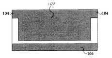
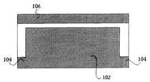
【0034】
本主題の他の実施形態は、図6Aないし図6Cにそれぞれ示す多層コンデンサ構成に関するものであり、これらは、図5Aないし図5Cの多層コンデンサ構成をそれぞれ改良したものである。開示する技術の追加の実施形態を、図7Aおよび図7Bのコンデンサアレイに関して提示する。そして、図8Aおよび8Bは、本主題に係るメッキ端子フィーチャの態様を示し、図9Aおよび図9Bは、本主題に係る選択的に端子形成した集積受動電子コンポーネントに関するものである。
【0035】
本明細書に提示する実施形態は、それぞれ、開示する技術を限定するものではないことに留意されたい。一実施形態の一部として図示又は説明した特徴は、別の実施形態と組み合わせることにより、他の実施形態とすることができる。加えて、ある特徴は、言及しなかったが同一、同様、又は等価の機能を有する同様のデバイスと置換することができる。
【0036】
開示する技術の現時点で好ましい実施形態を詳細に説明する。図1Aは、多層インタディジテイティッドコンデンサまたはコンデンサアレイで使用するための電極タブ14を備えた電極層10および12の既知の構成例を示す。各電極層には、各電極層と同一平面をなすとともに、電極層10および12ごとに列状に整列するようにタブ14が突出させてある。図1Aには、このようなタブを有する4つの電極層を示すが、本技術とともに利用される典型的な構成の中には、多くの電極層およびタブを含むことができる構成もある。この特徴によれば、オプションとして、(電極数を選択することにより)広範囲のキャパシタンスを有する容量性素子を作成することができる。
【0037】
図1Aの電極層構成は、完成したコンデンサの例を示すものではない。図1Aは、コンデンサおよびコンデンサアレイの構成例の中間態様を参照するためのものである。図1Aの電極層構成は、図1Bに示すような多層インタディジテイティッドコンデンサの例に従って利用することができる。
【0038】
インタディジテイティッドコンデンサは、典型的には、図1Aに示すような複数の電極層からなり、図1Bのインタディジテイティッドコンデンサ構成16にみられるような誘電材料18の本体中に配置されている。電極層10および12は、タブ14がIDC16の2つの面まで延在して露出するように、誘電材料18中に配置されている。このような電極層の材料の例としては、白金、ニッケル、パラジウム銀合金その他の適正な導電物質を含めることができる。誘電材料18としては、チタン酸バリウム、酸化亜鉛、低焼成ガラスを有するアルミナ、その他の適正なセラミック材料またはガラス結合材料を含めることができる。あるいはまた、誘電体は、有機化合物、例えば回路板材料として一般的なエポキシ(セラミックを混入したものとそうでないもの、繊維ガラス入りとそうでないもの)とするか、誘電体としての他のプラスティックとすることができる。これらの場合には、導体は、典型的には、化学的にエッチングしてパターンを形成するための銅箔である。
【0039】
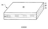
あるいはまた、IDC16においては、部分20が、電極層と誘電層を交互に重ねて多層構成としたものと見ることができる。IDC16は、さらに、典型的には、最上層の誘電層22と、最下層の誘電層24に特徴があり、これらの層はIDC16の他の層よりも一般的に厚くすることができる。誘電層22および24は、当該デバイスを保護する被覆層として働くから、コンデンサ本体に焼成されるガラス/金属フリット(frit)の応力に耐えるのに充分なバルク(bulk)を提供する。既知のコンデンサの例は、図1Bの多層構成を利用しているが、本主題においては、このような構成16の態様を、本明細書に開示する追加の特徴に従って利用する。
【0040】
図1Bのような多層IDCコンポーネント16は、図1Aの既知の電極層構成を組み入れたものであるが、IDCコンポーネント16の2つの選択面に露出した電極部分14を特徴とする。内部電極構成の他の例は、多層電子コンポーネントにおいて採用できるものであるが、内部電極部分が、異なる位置および/または異なる数のデバイス面で露出するようにすることもできる。
【0041】
例えば、図3Aの分解図に示す内部電極層構成を考察する。電極層26および28が交互に設けてあり、電極タブ部分30が1つの選択方向に延在させてある。電極層のセットの電極タブ30は、スタック構成にし、これにより、例えば電極層26のタブ30が2つの列でそれぞれ整列するのが好ましい。電極層28のタブ30についても、同様の整列状態が維持される。図3Aの内部電極構成を利用する多層コンデンサその他の受動電子コンポーネントは、典型的には、電極タブ部分30が電子コンポーネントの1つの選択面に露出するように構成されている。
【0042】
内部電極層構成の別の例では、電極タブが、多層インタディジテイティッド電子コンポーネントの4つの面に露出させることができる。このような内部電極層は、その構成を、電極層10および12の突出させたタブ部分が電極層10及び電極層12ごとに隣接するようにした図1Aと同様にすることができる。図5Aないし図5Cは、他の電極層構成の例と、対応する多層コンデンサの例をそれぞれ示す。図5Aに示すような複数の第1内部電極層32が、図5Bに示すような内部電極層34と、誘電材料36の本体中で交互に配置されて、図5Cに示すような多層コンデンサ38が形成される。このような多層コンデンサ38においては、あるセットを構成する電極層32または34の一部40が、多層コンデンサ38の面42に露出している。そして、多層コンデンサ38の面42と対向する面(図5Cでは見えない)には、他のセットを構成する電極層32または34の一部が露出している。
【0043】
図1Bを説明する。IDC16その他のモノリシック電子コンポーネントのための典型的な慣用の端子は、銀、銅その他の適正な金属のプリント厚膜ストライプ又は焼成厚膜ストライプをガラスマトリックスに備え、ガラスマトリックスの上部は、耐浸出性を高めるために、ニッケルで層状にメッキされ、このニッケル層の上に、錫またははんだ合金の層が形成され、この層によりニッケルの酸化が防止され、はんだ付けが容易になる。
【0044】
この種の端子形成に係る厚膜ストライプは、典型的には、端子形成機械およびプリントホイールによるプリントが必要であり、あるいは金属粉(metal-loaded)ペーストの転写に適した他のコンポーネントが必要である。このようなプリント用ハードウェアの分解能には限界があるから、厚膜ストライプを特に小さいチップに設けるのは困難である。IDC16その他の電子コンポーネントは、対向する側面の間の現行の典型的なサイズが、約120mil(1inch(2.54cm)の1/1000)(3.048mm)×60mil(1.524mm)であり、上層と下層の間の厚さが約30mil(0.762mm)である。このサイズの部品に5つ以上の端子を形成する必要があるか、あるいはより小さい寸法の部品に端子が所望されるとき、専用の端子形成機械の分解能に限界があるため、多くの場合、端子ストライプを効率的に設けることができない。
【0045】
本主題によれば、このような典型的な厚膜端子ストライプを設けないか簡略化する端子形成手法が提供される。充分に制御できない厚膜ストライプを設けないので、典型的な端子プリント用ハードウェアは必要がない。開示する技術に係る端子フィーチャは、ニッケル、錫、銅などのメッキ層であって、典型的には、厚膜端子ストライプ上に形成されるメッキ層に焦点を合わせている。
【0046】
図7Aのコンデンサアレイ44の構成を考察する。コンデンサアレイ44は、複数の内部電極と、対応する電極タブ46とが誘電材料48の本体に埋め込まれていることを特徴とする。IDC16の電極層に対して、コンデンサアレイ44の各電極タブ46は、典型的には、別々の内部電極に対応する。同様に露出した電極タブを備えたコンデンサアレイ44その他の電子コンポーネントを、例えばニッケルまたは銅イオン溶液のような無電解メッキ溶液に浸漬することにより、図7Bに示すようなメッキ端子50が形成されることが好ましい。このような溶液に浸漬することにより、露出した電極タブ46に、ニッケル、銅、錫その他の金属メッキ材料を堆積させることができる。このメッキ材料の堆積は、スタック列中の隣接する電極タブ46間が電気的に接続されるだけの堆積であるのが好ましい。適正にメッキされるためには、電極タブ列中の隣接する電極タブ間の距離は、約10ミクロン以下であるのが好ましい。したがって、端子50どうしが繋がらないようにするためには、電極タブ46の隣接するスタック列間の距離を、この最小距離の少なくとも2倍にするべきである。本技術の幾つかの実施形態では、露出メタライゼーションの隣接するスタック列間の距離は、特定のスタック中の隣接する露出電極タブ46間の距離の約4倍である。露出した内部導体部分の間の距離を制御して、端子の接続性を操作することにより、所望の端子構成に応じて、ブリッジした端子か、又はブリッジしていない端子を形成することができる。
【0047】
したがって、メッキ端子50は、露出した電極タブ46の配置によってガイドされる。以下、この現象を「自己決定的(self-determining)」という。というのは、メッキ端子50の形成は、多層電子コンポーネントまたはコンデンサアレイ44の選択面における露出メタライゼーションの構成によって決定されるからである。露出した内部電極タブ46は、端子50をコンデンサアレイ44′の外面に固定するのにも役立つ。コンデンサアレイ44′は、図7Aに44で示す多層コンデンサに、メッキ端子50が設けられたものである。抵抗値を低減するための添加剤をメッキ溶液に加えることにより、メッキ被覆および金属結合をさらに完全なものにすることができる。本主題のメッキ端子を形成する金属堆積の接着性を向上させるための他のメカニズムは、その後に、ベーク、レーザ露光、UV照射、マイクロ波照射、アーク溶接のような技術に従って、電子コンポーネントを加熱するものである。
【0048】
図7Bのメッキ端子50は、電子コンポーネントの幾つかの応用例のためには、充分に形成可能なものであるが、本技術の自己決定的端子を形成するには、内部電極タブからの露出メタライゼーションが不充分なこともある。このような場合においては、モノリシック電子コンポーネントの選択部分にアンカータブを埋め込むことが有益である場合がある。アンカータブは、短い導電タブであって、典型的には電子コンポーネントに電気的な機能を提供するものではないが、機械的な核となるものであり、モノリシックデバイスの外面に追加のメッキ端子を固定するものである。露出したアンカータブは、露出した内部電極部分と共に、より効果的な自己決定的端子を作成できるだけの露出メタライゼーションを施すことができる。
【0049】
例えば、図2Aの内部メタライゼーションの分解組立構成を考察する。電極層52および54は、図1Aの電極層と同様の構成になっており、電極タブ部分56が電極層52および54の選択位置から延在させてある。多層電子コンポーネントの選択位置で露出するが、内部において電気的に接続されないようにするため、アンカータブ58も、活性電極層52および54と同一平面に設けられるのが好ましい。電子コンポーネントの外面に延在させた自己決定的メッキ端子の形成が可能になるように、追加のアンカータブを、多層電子コンポーネントのカバー層に設けて、選択面に露出させることもできる。
【0050】
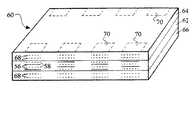
図2Bを説明する。多層電子コンポーネント60は、本主題に係る多層コンデンサに対応する。多層電子コンポーネント60の部分62は、誘電材料の一部に埋め込まれた図2Aのインタディジテイティッド電極層およびアンカータブの構成を含むことが好ましい。部分62の外面に見られる実線56は、図2Aの電極タブ56の露出部分を示し、部分62の外面に見られる破線58は、露出したアンカータブ58を示す。追加のアンカータブを誘電カバー層64および66に埋め込んで(この露出部分を破線68で示す)、本主題に係る自己決定的メッキ端子の形成を容易にするための露出メタライゼーション構成をさらに提供することもできる。内部アンカータブは、全ての内部タブが幾つかの共通スタックに構成されるように、内部電極タブのスタックと同様の列状に整列されるのが好ましい。
【0051】
電子コンポーネントの応用例においては、端子を電子コンポーネントの幅全体に亘って設けるだけでなく、上層と下層を抱く(wrap-around)ようにするのが好ましい。この場合、メッキ端子を多層IDC60の上層と下層に設け、はんだランドを延在させることができるから、外部アンカータブ70を、多層IDC60の上層と下層に設けることができる。例えば、エンベッド(embed)された内部アンカータブ58および68と、外部アンカータブ70とを、図2Bに示すようなIDC60の既存の露出電極タブ56に設けると、図8Aに示すような抱き(wrap-around)メッキ端子72を容易に形成することができる。
【0052】
メッキ端子、例えば図8Aの多層電子コンポーネント74に設けた端子72を形成するのに使用できる可能性のある技術としては、幾つか異なる技術がある。前述したが、第1の方法は、電気メッキまたは電気化学的堆積の技術であり、これら技術においては、露出した導電部分を有する電子コンポーネントを、メッキ溶液、例えば電気的バイアスに特徴がある電解ニッケルまたは電解錫に浸漬する。ついで、メッキ溶液と逆の極性のバイアスを電子コンポーネント自体にかける。すると、メッキ溶液中の導電要素が、電子コンポーネントの露出メタライゼーションに引き付けられる。このようなメッキ技法で極性バイアスを伴わないものは、無電解メッキと呼ばれ、ニッケルや銅イオン溶液のような無電解メッキ溶液と共に採用することができる。
【0053】
電気化学的な堆積技法および無電解メッキ技法に従って、図8AのIDC74のような電子コンポーネントを、特定の時間、適正なメッキ溶液に浸漬するのが好ましい。本主題の実施形態においては、メッキ材料を露出導電位置に対して垂直な方向に広げて、選択された隣接する露出導電部分の間を接続できるだけ蓄積させるため、メッキ材料を、電子コンポーネントの露出導電位置に充分に堆積させるのに、15分しか必要でない。
【0054】
本主題のメッキ端子形成に従って利用できる別の技法には、メッキ材料の磁気吸引が含まれる。例えば、処理槽の溶液中に懸濁しているニッケル粒子は、ニッケルに磁気特性があるから、多層電子コンポーネントと同様に、導電性の露出電極タブおよびアンカータブに引き付けられる。他の同様の磁気特性を有する材料もメッキ端子の形成に採用することができる。
【0055】
メッキ端子材料を多層電子コンポーネントの露出電極タブおよびアンカータブに追加することに関する他の技法としては、電気泳動または静電気の原理を利用するものがある。このような技術においては、処理槽溶液に、静電帯電した粒子が含まれる。この場合、帯電粒子が電子コンポーネントの選択位置で堆積するように、露出した導電部分を有するIDCその他の多層電子コンポーネントに、逆の極性でバイアスをかけて処理槽溶液に浸漬することができる。この技法は、ガラスと、他の半導電材料または離間材料の応用例において特に有用である。一度このような材料が堆積されると、電子コンポーネントを充分に加熱すれば、この堆積された材料を導電材料に変換できる。
【0056】
開示する技術に係るメッキ端子を形成する1つの方法は、前述のメッキ技法を組み合せたものに関する。まず、多層電子コンポーネントを、銅イオン溶液のような無電解メッキ溶液に浸漬して、銅の最初の層を露出タブ部分の上に堆積させると、より大きな接触領域が得られる。ついで、このメッキ技法を電気化学的メッキシステムに切り替えると、銅を、より高速に、この電子コンポーネントの選択部分に蓄積させることができる。
【0057】
本技術に係る多層電子コンポーネントの露出メタライゼーションに、材料をメッキするのに利用可能な異なる技法によれば、メッキ端子を作成するため、及び電子コンポーネントの内部フィーチャを電気的に接続するため、異なる材料を使用することができる。例えば、ニッケル、銅、錫のような金属導体を利用することができ、同様に、適した抵抗導体または半導電材料、および/あるいはこれら異なるタイプの材料を選択的に組み合せたものを利用することができる。
【0058】
本主題に係るメッキ端子であって複数の異なる材料を含むメッキ端子の例について、図8Bを参照して述べる。図8Bは、図8Aの電子コンポーネント74のA−A線断面図であり、メッキ端子72の実施形態に係るものである。当然のことであるが、端子72は、この例で示すように、追加の層は含まず、最初のメッキ層だけを含んでいる。図8Aおよび図8Bの多層電子コンポーネントおよび端子の実施形態においては、メッキ層の層数が変化する可能性があるから、それぞれ、参照番号として74および74′を付してあるが、これは、これら2つの実施形態の一方が他方と異なることを暗示するものではない。
【0059】
図8Bに示す端子形成における第1のステップは、無電解銅メッキ溶液中に電子コンポーネントを浸漬し、これにより、電子コンポーネント74′の外面において、内部アンカータブ58および68と、電極層52および54から延在させ露出させた内部電極タブと、外部アンカータブ70とが露出するところで、銅その他の金属の層76を堆積させることを含む。そこで、金属メッキ76で被覆されたタブ領域を、抵抗器高分子材料78で被覆し、再び、金属銅その他の材料80でメッキすることができる。
【0060】
他のメッキ代替法においては、金属メッキ層が形成され、このような金属メッキの上に抵抗合金が電気メッキされる。メッキ層は、種々の異なるメッキ端子構成を得るため、単独で設けることもでき、組み合わせて設けることもできる。このようなメッキ端子の基本となるものは、電子コンポーネントの外面に、露出させた導電部分を設計するとともに配置することにより、自己決定的なメッキを構成することである。
【0061】
本主題に係るメッキ端子を容易に形成するため、種々の異なる構成において、内部電極部分およびアンカータブをこのように配向することができる。例えば、電極層26および28を有する図3Bの内部導電構成を考察する。電極タブ30および内部アンカータブ82を誘電材料の本体に設けて、図4Aと同様の多層電子コンポーネントを作成することができる。内部アンカータブ84および外部アンカータブ86も追加して設けることができる。この場合、所定のメッキ技法の1つを利用して、多層電子コンポーネント88に露出したメタライゼーション領域にメッキ端子を形成することができる。
【0062】
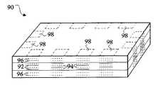
図4Bは、本主題の態様に係る別の多層電子コンポーネントを、電子コンポーネント90として示す。内部電極層は、電子コンポーネント90の4つの面にまで延在させた電極タブを有する。追加した内部アンカータブ94と、露出させた電極タブ92とを交互に配置することができる。他の内部アンカータブ96を電子コンポーネント90の被覆層にエンベッド(embed)して、メッキ端子を延長させることもできる。外部アンカータブ98を設けることにより、抱き(wrap-around)メッキ端子を容易に形成することができる。
【0063】
ここに開示する技術の他の応用例は、一般的な多層電子コンポーネント構成、例えば図6A、図6B、図6Cに示すような構成に関するものである。図6Aの電極層100と、図6Bの電極層102とが、それぞれ、電極層から電極タブ部分104へ延在させるため、それぞれT字形に構成されている。電極層100および102と誘電層とが交互に配置され、図6Cに示すような多層デバイスが形成される場合には、各電極タブ部分104がデバイス108の2つの隣接面に露出する。アンカータブ部分106を電極層平面内に設けることもでき、これにより、露出した導電部分がデバイス108の対向面で整列するから、この対向面上に容易にメッキ電極を形成することができる。
【0064】
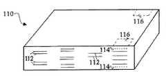
開示する技術の別の実施態様を、図9Aおよび図9Bに関して提示する。図9Aは、単一のモノリシック構造内に設けた受動電子コンポーネントを組み合せたものを含む集積受動電子コンポーネント110を示す。集積電子コンポーネント110は、抵抗器、バリスタ、コンデンサ、インダクタ、カプラ、バラン、および/またはその他の受動電子コンポーネントの選択された組み合せたものを含むことができる。異なる受動電子コンポーネントは、それぞれ、典型的には、少なくとも1つの導電電極様の部分を特徴とし、この部分から少なくとも1つの電極タブ部分112が延在され、電子コンポーネント110の外面に露出する。
【0065】
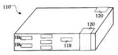
図9Aに示すような集積受動電子コンポーネント110は、図示したように、複数の異なる内部電極構成を有することができる。対応する電極タブ112を、対称または非対称に設けることができ、種々にグループ化することができる。重要な特徴は、露出する電極タブ112を電子コンポーネント110内で構成して、メッキ端子を選択的に容易に形成することができることにある。加えて、集積受動電子コンポーネントに内部アンカータブ114および/または外部アンカータブ116を設けて、追加の端子構成を選択的に形成することもできる。例えば、多くの露出した内部電極タブ112と、内部アンカータブ114と、外部アンカータブ116とを有する図9Aの露出タブ構成を考察する。ここに開示する種々の技術によれば、このような構成をメッキ溶液に浸漬すると、好ましくは、メッキされた複数の端子118と、メッキされた抱き(wrap-around)端子120、例えば図9Bに示すような端子が形成されることになる。集積受動電子コンポーネントまたは多層電子デバイス110′は、単に、図9Aに110で示す集積受動電子コンポーネントに、メッキ端子118および120がそれぞれ追加されたものに対応する。そこで、集積受動電子コンポーネントのタブは、メッキ端子を、異なる電極間、及び異なる電子コンポーネント層間に形成できるように、設計することができる。
【0066】
図1Aないし図9Bにそれぞれ提示するモノリシック電子コンポーネントの実施形態は、当然、開示した技術にすぎず、これらの中間態様も含む。これらの例においては、多くの場合、4つ以上の一般的な電極列を示しているが、所望の電子コンポーネント構成に応じて、電極列の数を増減することも可能である。開示した技術によれば、選択された任意の電子コンポーネント面の任意の選択部分に沿ってメッキ端子を形成することが可能である。このようなメッキ端子は、単層のメッキ導電材料、抵抗材料、または半導電材料、あるいはこのような材料から選択的に組み合わせた多層のものも含むことができる。
【0067】
当然のことであるが、内部アンカータブおよび外部アンカータブを、異なる端子プレファランス(preference)のために選択的に使用して、種々のサイズの端子または抱き(wrap-around)端子を設けることができる。本明細書に図示は記載した、内部アンカータブと外部アンカータブの両方のアンカータブを特徴とするIDCは、例えば、特定の応用例において抱き(wrap-around)端末が好ましくないときは、内部アンカータブフィーチャのみを利用することができる。異なる多層電子コンポーネント上で、内部及び外部アンカータブの両方と既存の露出電極タブとを種々に組み合わせることにより、1つのデバイスに対して、多くの端子スキームが可能になる。
【0068】
以上、本主題をその具体的な実施形態に関して詳細に述べたが、このような実施形態を改変し、変形し、均等物を得るために、本技術を容易に適合させることができる、ことは当業者にとって当然のことである。したがって、本開示の範囲は、限定するものではなく、例にすぎず、本開示は、本主題を修正し、変形し、および/または追加することを妨げるものではない。このことは当業者に顕著である。
【図面の簡単な説明】
【図1A】多層インタディジテイティッドコンデンサにおける既知の電極層構成の分解図である。
【図1B】図1Aに示した既知の実施形態のような内部電極層構成を有する多層インタディジテイティッドコンデンサの外観図である。
【図2A】本主題に係る多層インタディジテイティッドコンデンサについての内部電極層およびアンカータブ構成の分解図である。
【図2B】図2Aに示したような内部電極およびアンカータブ部分を有する本主題に係る多層インタディジテイティッドコンデンサの外観図である。
【図3A】多層コンデンサにおける既知の内部電極層構成の分解図である。
【図3B】本主題に係る多層コンデンサにおける内部電極層およびアンカータブ構成の分解図である。
【図4A】図3Bに示したような内部電極およびアンカータブ部分を有する本主題に係る多層コンデンサの外観図である。
【図4B】本主題に係る多層インタディジテイティッドコンデンサの外観図であり、コンデンサ構成の4つの選択面に露出した内部電極およびアンカータブ部分を特徴とする外観図である。
【図5A】多層コンデンサの例で用いるための既知の電極構成の上面図である。
【図5B】多層コンデンサの例で用いるための既知の電極構成の上面図である。
【図5C】図5Aおよび図5Bの例のような電極層構成を有する多層コンデンサの例の外観図である。
【図6A】多層コンデンサの例で用いるための本主題に係る電極層構成の上面図である。
【図6B】多層コンデンサの例で用いるための本主題に係る電極層構成の上面図である。
【図6C】図6Aおよび6Bに示したような電極層構成を有する本主題に係る多層コンデンサの例の外観図である。
【図7A】電極タブが露出したコンデンサアレイの外観図である。
【図7B】本主題に係るメッキ端子を有するコンデンサアレイの外観図である。
【図8A】本主題に係るメッキ端子を有する多層インタディジテイティッドコンデンサの外観図である。
【図8B】図8AのA−A線断面図であって、本開示技術に係るメッキ端子を有する多層インタディジテイティッドコンデンサの断面図である。
【図9A】本開示技術に係る露出した電極タブと追加のアンカータブとを有するモノリシック集積受動電子コンポーネントの概略面図であって上面透視図もわずかに含む図である。
【図9B】本主題に係るメッキ端子を有するモノリシック集積受動電子コンポーネントの外観図である。
【符号の説明】
10、12 電極層
14 電極タブ
16 インタディジテイティッドコンデンサ(IDC)
18 誘電材料
22 最上部の誘電層
24 最下部の誘電層
26、28 電極層
30 電極タブ
32、34 内部電極層
36 誘電材料
38 多層電子コンポーネント
40 電極層
44、44′ コンデンサアレイ
46 電極タブ
48 誘電材料
50 メッキ端子
52、54 電極層
56 電極タブ
58 アンカータブ
60 多層電子コンポーネント
64、66 誘電被覆層
68 内部アンカータブ
70 外部アンカータブ
72 抱きメッキ端子
74 多層電子コンポーネント
76 金属層
78 抵抗器高分子材料
80 金属銅
82、84 内部アンカータブ
86 外部アンカータブ
88 多層電子コンポーネント
90 多層電子コンポーネント
92 電極タブ
94、96 内部アンカータブ
98 外部アンカータブ
100、102 電極層
104 電極タブ
106 アンカータブ
108 デバイス
110、110′ 集積受動電子コンポーネント
112 電極タブ
114 内部アンカータブ
116 外部アンカータブ
118、120 メッキ端子[0001]
BACKGROUND OF THE INVENTION
The present subject matter relates generally to improved terminal features for multilayer electronic components, and specifically to plated terminals for multilayer capacitors or integrated passive components. The subject terminal design utilizes selective configuration of internal and / or external electrode tabs to facilitate the formation of plated electrical connections. An external connection is preferably formed, which eliminates or greatly simplifies the normal thick film terminal stripe.
[0002]
[Prior art]
Modern components are often packaged as monolithic devices and may include a single component or multiple components within a single chip package. A specific example of such a monolithic device is a multilayer capacitor or capacitor array, of particular importance with respect to the disclosed technology is a multilayer capacitor with an interdigitated internal electrode layer and a corresponding electrode tab. is there. Examples of multilayer capacitors including features of interdigitated capacitor (IDC) technology can be found in US Pat. Other monolithic components correspond to devices that integrate multiple passive components in a single chip structure. Such integrated passive components can be realized as a selected combination of resistors, capacitors, inductors, and / or other passive components formed in a multilayer configuration and packaged as a monolithic electronic device.
[0003]
Selective terminals are often required to form electrical connections for various monolithic components. Multiple terminals are required to provide electrical connection to each component of an integrated monolithic device. Multiple terminals are often used with IDCs and other multilayer arrays to reduce undesirable inductance. An example of a scheme that has been used to form multiple terminals in a multilayer component is to drill a via through a selected area of the chip structure and fill the via with a conductive material to select a device. An electrical connection is formed between the electrode portions.
[0004]
Another way to form external terminals for the target device is to add a thick film of silver or copper film on a glass matrix to the exposed portion of the internal electrode layer, followed by plating an additional metal layer over the terminal stripe. Thus, a certain part can be soldered to the substrate. An example of a component including an external electrode formed of a baked terminal and a metal film plated thereon is disclosed in Patent Document 3. Adding terminals is often difficult to control, and problems can arise as the chip size is reduced.
[0005]
Since the component size is constantly reduced, it is very difficult to print the terminal stripe in a predetermined area with the required accuracy. Thick film terminal stripes are typically added by a machine that grabs the chip and selectively adds terminals with a specially designed wheel. The mechanical mechanisms and steps relating to adding terminal stripes to the chip structure are disclosed in US Pat. As the component size of an electronic chip device decreases or the number of terminal contacts increases, typically the resolution of the terminal forming machine reaches its limit.
[0006]
Problems that arise when selectively forming terminals include misalignment of terminal lands, misplaced terminals, thereby exposing or completely missing internal electrode tabs, and hugging ( wrap-around) is missing. Furthermore, if the coating of the terminal paint-like material is too thin, or if another part of the terminal coating is soiled and the terminal land is short-circuited, another problem may occur. Another problem with thick film systems is that it is often difficult to form terminals only on selected surfaces of the device, such as the vertical plane. With regard to providing electrical terminals in monolithic devices, there is a need to provide cheap and efficient terminal features for electronic chip components.
[0007]
Another option known for terminal formation is to align a plurality of individual substrate components to a shadow mask. Each part can be mounted in a specially designed fixture as disclosed in
[0008]
[0009]
Other background references that are directed to methods of forming multilayer ceramic devices include US Pat.
[0010]
Various aspects and alternative features are known in the field of electronic components and their terminals, but no single design can address any of the issues described herein. The disclosures of the aforementioned US patents are numbered and made a part of this specification.
[0011]
[Patent Document 1]
US Pat. No. 5,880,925
[Patent Document 2]
US Pat. No. 6,243,253 B1
[Patent Document 3]
US Patent No. 5021921
[Patent Document 4]
US Pat. No. 6,232,144 B1
[Patent Document 5]
US Pat. No. 6,214,685 B1
[Patent Document 6]
US Pat. No. 5,994,897
[Patent Document 7]
US Pat. No. 5,863,331
[Patent Document 8]
US Pat. No. 5,753,299
[Patent Document 9]
US Pat. No. 5,226,382
[Patent Document 10]
US Pat. No. 4,919,076
[Patent Document 11]
US Patent No. 5880011
[Patent Document 12]
US Pat. No. 5,770,476
[Patent Document 13]
US Pat. No. 6,141,846
[Patent Document 14]
US Pat. No. 3,258,898
[Patent Document 15]
U.S. Pat. No. 4,811,164
[Patent Document 16]
U.S. Pat. No. 4,266,265
[Patent Document 17]
U.S. Pat. No. 4,241,378
[Patent Document 18]
U.S. Pat. No. 3,988,498
[0012]
[Problems to be solved by the invention]
The present subject matter is to recognize and solve the various problems described above, and to recognize and address the formation of electrical terminals and other related aspects of the related art. Thus, the primary purpose of some embodiments of the disclosed technology is generally in the terminal features of electronic components. Specifically, since the disclosed terminal features are only plated, typically the thick film stripes printed on a portion of the monolithic device for terminal formation are removed or significantly removed. Designed to be simplified.
[0013]
[Means for Solving the Problems]
Another primary objective of the disclosed technique is to provide a method for guiding the formation of plated terminals by providing internal electrode tabs and optionally placing additional anchor tabs. Both the internal electrode tab and the additional anchor tab can facilitate the formation of a fixed and reliable outer plating. Anchor tabs are typically not electrically connected internally, but providing anchor tabs can improve the connectivity of the external terminals and improve mechanical integrity and deposition of plating material. it can.
[0014]
Another object of the present subject matter is to provide a terminal feature in an electronic component that eliminates or simplifies the typical thick film terminal stripe, requiring only plated terminals to connect to external electrodes. Plating materials according to the disclosed techniques include metal conductors, resistive materials, and / or semiconductive materials.
[0015]
Another object of the subject terminal technology is that terminal features can be used in accordance with various multilayer monolithic devices, including, for example, interdigitated capacitors, multilayer capacitor arrays, and integrated passives. Contains components. Integrated passive components can include resistors, capacitors, varistors, inductors, baluns, and / or selectively combinations of other passive components.
[0016]
An advantage gained by the disclosed subject matter is that the terminal features of the electronic component can be provided without terminal formation on a terminal forming machine, resulting in an external terminal with unusual resolution. When the terminal resolution is improved as described above, more terminals can be provided in a predetermined component region, and the terminals can be provided at a finer pitch.
[0017]
A general object of the present technology is to provide a terminal feature that enables a solder base with reduced solder leaching effects. The exposed electrode portion and anchor tab portion are designed such that the plated terminal material adheres to selected adjacent exposed tab portions without unnecessarily bridging between different terminal locations.
[0018]
Another object of the present subject matter is that the disclosed technology can be utilized in accordance with many different terminal configurations, including various numbers and arrangements of external terminals. The plated terminals can be formed at self-determined locations by providing conductive elements that are exposed on the outer surface of the electronic component in accordance with various different plating techniques disclosed herein.
[0019]
Another object of the subject plating technology is to facilitate the manufacture of cheaper and more efficient electronic components in a proper and reliable manner.
[0020]
Other objects and advantages of the present invention will be apparent to those skilled in the art from this detailed description as set forth in the detailed description herein. It will also be apparent to those skilled in the art that the specific examples, references, and features discussed and / or steps may be based on reference to the disclosed technology without departing from the spirit and scope thereof. It can be implemented in various embodiments and uses. Such variations include replacing equivalents of the means, steps, or features, or equivalents shown, referenced, or discussed, and various parts, features, steps. But not limited to, such as, but not limited to, functional, operational or positional inversion.
[0021]
In addition, the following is natural. That is, the various embodiments of the present technology and the presently preferred embodiments are combinations or equivalents of the steps, features or elements disclosed herein (not specifically shown and not described in detail). Including combinations of features or configurations of the present invention). A first embodiment of the present subject matter relates to a plated terminal for a multilayer electronic component. Such a multilayer electronic component preferably includes a plurality of spaced substrates, and electrodes are respectively disposed between the plurality of spaced substrates. Each of the electrodes preferably has at least one tab portion extending from the electrode and exposed at a selected end of the plurality of spaced apart substrates. The selected tab portions of the exposed tab portions are preferably stacked at a predetermined distance from each other so that a plurality of plated terminals can be formed on the outer surface of the electronic component.
[0022]
Another embodiment related to the disclosed technology relates to an electronic component like the first embodiment described above, and further includes an additional anchor tab. In such an embodiment, the anchor tab can also be disposed between the plurality of substrate layers and exposed at a predetermined position, so that the plating is performed depending on the exposed electrode tab portion and the position of the exposed anchor tab. The formation of the terminal is guided. By providing a sufficient stack of exposed tabs and exposed tabs on the top and bottom surfaces of the dielectric material body aligned with the stack of exposed tabs, a plated terminal is formed on the entire exposed surface and the top surface of the electronic component. It is possible and desirable (although not necessarily) to form plated terminals that wrap-around both.
[0023]
Another embodiment of the invention corresponds to an integrated monolithic device that includes at least two passive electronic components. Each passive electronic component is characterized by a ceramic portion and characterized by at least one internal electrode layer extending from the internal electrode layer and having a tab portion exposed to at least one selected surface of the integrated monolithic device. Is preferred. Each passive electronic component of the monolithic device preferably includes a plurality of metallizing portions formed to selectively connect a plurality of tab portion sets and to electrically connect to the electrode layers of each passive electronic component. To provide additional terminal options, the anchor tab can also be utilized in accordance with the previously described example of an integrated monolithic device. By placing the internal electrode tabs at selected locations within the monolithic device, a variety of different terminal options are available. The formation of the plated terminals is guided by the position of the exposed electrode tabs and anchor tabs, and in some cases can be wrapped around the top and bottom surfaces of the monolithic device.
[0024]
Another embodiment of the present subject matter relates to an interdigitated capacitor in which a plurality of electrode layers and a plurality of dielectric layers are alternately provided, the interdigitated capacitor having features in the uppermost layer and the lowermost layer. It is. The uppermost layer and the lowermost layer of the multilayer interdigitated capacitor preferably include a dielectric cover layer that is thicker than the other dielectric layers stacked. Each of the electrode layers includes a plurality of electrode tabs that extend to the selection surface of the interdigitated capacitor. The electrode tab is preferably exposed at a stack portion at a selected position along the face of the capacitor. Anchor tabs are preferably embedded in the upper and lower cover layers, and optionally are embedded in the active layer such that the exposed tab stack is exposed at the face of the multilayer device. The exposed tab stack can then be plated with external terminals, and if the anchor tabs are placed on the top and bottom layers and aligned with the exposed stack of internal tabs, the top and bottom layers You can wrap-around.
[0025]
Other embodiments of the present subject matter are not necessarily mentioned in the Measures section to solve the problem, but are referred to herein for features or parts referred to for purposes above and / or otherwise. Various combinations of aspects of features or parts can be included.
[0026]
Those skilled in the art will understand the features, aspects, and the like of such embodiments upon review of the remainder of the specification.
[0027]
A complete and practicable description of the present subject matter, including its best mode, is presented herein for those skilled in the art. Reference is made herein to the attached figures.
[0028]
Repeat use of reference characters in the present specification and the accompanying drawings shall represent the same or similar features or elements of the present invention.
[0029]
DETAILED DESCRIPTION OF THE INVENTION
As mentioned in the Measures section, the present subject matter is directed to improving terminal features for monolithic electronic components.
[0030]
The subject terminal approach utilizes exposed electrode portions of structures such as monolithic capacitor arrays, multilayer capacitor arrays with interdigitated electrode configurations, integrated passive electronic components, and other electronic chip structures. Is. Anchor tabs can be embedded in such monolithic electronic components for plating the exposed portions of the plurality of stacked internal conductive portions to form terminals and secure them to the face of the device.
[0031]
By providing additional anchor tabs on the top and bottom surfaces of the chip device, a wrap-around plated terminal can be formed, which leads from one of the upper or lower layers to the other through the side of the chip. Can do. In some applications, such hull-plated terminals are desirable to facilitate soldering of the chip to a printed circuit board or other suitable substrate.
[0032]
The subject plating techniques and anchor tab features can be utilized in accordance with different monolithic electronic components. 1A and 1B illustrate a known interdigitated electrode layer embodiment, in which electrode tabs are generally extended and exposed to two selected surfaces of a multilayer electronic component. . Following this, aspects of plated terminal formation in accordance with the present subject matter are presented with respect to FIGS. 2A and 2B, which also relate to multilayer electronic components having conductive portions exposed on two selected surfaces of the device.
[0033]
FIG. 3A shows an embodiment of a known electrode layer configuration with electrodes for exposure to one selective surface of a multilayer electronic device. FIGS. 3B and 4A each relate to an improvement of the embodiment shown in FIG. 3A, and in the multilayer capacitors of these embodiments, the internal electrode tabs are exposed on one selected face of the capacitor, It features such an anchor tab. FIG. 4B relates to a multi-layer interdigitated component that has an internal electrode tab and an anchor tab exposed on the four selected surfaces of the component according to the present subject matter.
[0034]
Other embodiments of the present subject matter relate to the multilayer capacitor configurations shown in FIGS. 6A-6C, respectively, which are improvements to the multilayer capacitor configurations of FIGS. 5A-5C, respectively. Additional embodiments of the disclosed technology are presented with respect to the capacitor array of FIGS. 7A and 7B. 8A and 8B illustrate aspects of plated terminal features according to the present subject matter, and FIGS. 9A and 9B relate to selectively terminalized integrated passive electronic components according to the present subject matter.
[0035]
It should be noted that each of the embodiments presented herein is not intended to limit the disclosed technology. Features illustrated or described as part of one embodiment may be combined with another embodiment to form another embodiment. In addition, certain features may be replaced with similar devices not mentioned but having the same, similar or equivalent functions.
[0036]
Reference will now be made in detail to presently preferred embodiments of the disclosed technology. FIG. 1A shows a known configuration example of electrode layers 10 and 12 with
[0037]
The electrode layer configuration of FIG. 1A does not show an example of a completed capacitor. FIG. 1A is for referring to an intermediate aspect of a configuration example of a capacitor and a capacitor array. The electrode layer configuration of FIG. 1A can be utilized in accordance with an example of a multilayer interdigitated capacitor as shown in FIG. 1B.
[0038]
An interdigitated capacitor typically consists of a plurality of electrode layers as shown in FIG. 1A and disposed in a body of
[0039]
Alternatively, in the
[0040]
A
[0041]
For example, consider the internal electrode layer configuration shown in the exploded view of FIG. 3A. Electrode layers 26 and 28 are alternately provided, and
[0042]
In another example of an internal electrode layer configuration, electrode tabs can be exposed on four sides of a multilayer interdigitated electronic component. Such an internal electrode layer can have the same configuration as that of FIG. 1A in which the protruding tab portions of the electrode layers 10 and 12 are adjacent to each other for each of the electrode layers 10 and 12. FIGS. 5A to 5C show examples of other electrode layer configurations and corresponding multilayer capacitors, respectively. A plurality of first internal electrode layers 32 as shown in FIG. 5A are alternately arranged in the body of the
[0043]
1B will be described. Typical conventional terminals for IDC16 and other monolithic electronic components include a printed or fired thick film stripe of silver, copper or other suitable metal in the glass matrix, the top of the glass matrix being leaching resistant In order to increase the resistance, nickel is layered and a tin or solder alloy layer is formed on the nickel layer, which prevents nickel oxidation and facilitates soldering.
[0044]
Thick film stripes for this type of terminal formation typically require printing by a terminal forming machine and a print wheel, or other components suitable for transfer of metal-loaded paste. is there. Since the resolution of such printing hardware is limited, it is difficult to provide a thick film stripe on a particularly small chip. IDC16 and other electronic components have a current typical size between opposing sides of approximately 120 mils (1/1000 of an inch) (3.048 mm) × 60 mils (1.524 mm), The thickness between the upper layer and the lower layer is about 30 mil (0.762 mm). When it is necessary to form more than 5 terminals on a part of this size, or when a terminal is desired for a smaller sized part, the resolution of a dedicated terminal forming machine is limited and often the terminal Stripes cannot be provided efficiently.
[0045]
In accordance with the present subject matter, a terminal formation technique is provided that eliminates or simplifies such typical thick film terminal stripes. Typical terminal printing hardware is not necessary because thick film stripes that cannot be sufficiently controlled are not provided. The terminal feature according to the disclosed technique is a plated layer of nickel, tin, copper, etc., typically focusing on the plated layer formed on the thick film terminal stripe.
[0046]
Consider the configuration of the
[0047]
Therefore, the plated
[0048]
The plated
[0049]
For example, consider the exploded assembly configuration of the internal metallization of FIG. 2A. The electrode layers 52 and 54 have the same configuration as the electrode layer of FIG. 1A, and an
[0050]
FIG. 2B will be described. The multilayer
[0051]
In electronic component applications, it is preferred that the terminals not only be provided across the width of the electronic component, but also wrap-around the upper and lower layers. In this case, since the plating terminals can be provided in the upper layer and the lower layer of the
[0052]
There are several different techniques that could be used to form plated terminals, such as the
[0053]
According to electrochemical deposition and electroless plating techniques, it is preferable to immerse an electronic component, such as
[0054]
Another technique that can be utilized in accordance with the subject plating terminal formation includes magnetic attraction of plating material. For example, nickel particles suspended in a solution in a processing bath are attracted to conductive exposed electrode tabs and anchor tabs, similar to multilayer electronic components, because nickel has magnetic properties. Other materials having similar magnetic properties can also be employed to form the plated terminals.
[0055]
Other techniques for adding plated terminal material to the exposed electrode tabs and anchor tabs of multilayer electronic components are those that make use of electrophoretic or electrostatic principles. In such a technique, the electrostatically charged particles are contained in the treatment tank solution. In this case, an IDC or other multilayer electronic component having an exposed conductive portion can be biased with the opposite polarity and immersed in the treatment bath solution so that charged particles are deposited at selected locations of the electronic component. This technique is particularly useful in glass and other semiconducting or spacing material applications. Once such a material is deposited, the deposited material can be converted to a conductive material if the electronic component is sufficiently heated.
[0056]
One method of forming a plated terminal according to the disclosed technology relates to a combination of the foregoing plating techniques. First, a larger contact area is obtained when the multilayer electronic component is immersed in an electroless plating solution, such as a copper ion solution, and a first layer of copper is deposited on the exposed tab portion. Then, when this plating technique is switched to an electrochemical plating system, copper can be accumulated in selected portions of the electronic component faster.
[0057]
According to the different techniques available for plating materials on the exposed metallization of multi-layer electronic components according to the present technology, different to create plated terminals and to electrically connect the internal features of the electronic components Material can be used. For example, metal conductors such as nickel, copper, tin can be used, as well as using suitable resistive or semiconductive materials and / or selective combinations of these different types of materials. Can do.
[0058]
An example of a plated terminal according to the present subject matter that includes a plurality of different materials will be described with reference to FIG. 8B. FIG. 8B is a cross-sectional view of the
[0059]
The first step in forming the terminal shown in FIG. 8B is to immerse the electronic component in an electroless copper plating solution, thereby causing
[0060]
In another plating alternative, a metal plating layer is formed and a resistance alloy is electroplated on such metal plating. The plated layers can be provided alone or in combination to obtain various different plated terminal configurations. The basis for such plated terminals is to design self-determining plating by designing and placing exposed conductive portions on the outer surface of the electronic component.
[0061]
In order to easily form a plated terminal according to the present subject matter, the internal electrode portions and anchor tabs can be oriented in this manner in a variety of different configurations. For example, consider the internal conductive configuration of FIG. 3B with
[0062]
FIG. 4B illustrates another multilayer electronic component according to aspects of the present subject matter as electronic component 90. The internal electrode layer has electrode tabs that extend to four sides of the electronic component 90. Additional internal anchor tabs 94 and exposed electrode tabs 92 can be alternately arranged. Other
[0063]
Other applications of the disclosed technology relate to general multilayer electronic component configurations, such as those shown in FIGS. 6A, 6B, and 6C. The
[0064]
Another embodiment of the disclosed technique is presented with respect to FIGS. 9A and 9B. FIG. 9A shows an integrated passive
[0065]
An integrated passive
[0066]
The monolithic electronic component embodiments presented in FIGS. 1A-9B, respectively, are of course only the disclosed technique and include these intermediate aspects. In these examples, four or more general electrode rows are shown in many cases, but the number of electrode rows can be increased or decreased depending on the desired electronic component configuration. According to the disclosed technique, a plated terminal can be formed along any selected portion of any selected electronic component surface. Such plated terminals can also include single layer plated conductive materials, resistive materials, or semiconductive materials, or multiple layers selectively combined from such materials.
[0067]
Of course, the inner and outer anchor tabs can be selectively used for different terminal preferences to provide various sized terminals or wrap-around terminals. it can. The IDC illustrated and described herein, which features both internal and external anchor tabs, can be used, for example, when a wrap-around terminal is not preferred in a particular application. Only tab features can be used. Various combinations of both internal and external anchor tabs and existing exposed electrode tabs on different multilayer electronic components allow many terminal schemes for a single device.
[0068]
Although the subject matter has been described in detail with reference to specific embodiments thereof, it should be understood that the technology can be readily adapted to modify, modify, and obtain equivalents to such embodiments. Of course for those skilled in the art. Accordingly, the scope of the present disclosure is not intended to be limiting, but merely examples, and the present disclosure does not preclude modifications, variations, and / or additions to the subject matter. This is remarkable for those skilled in the art.
[Brief description of the drawings]
FIG. 1A is an exploded view of a known electrode layer configuration in a multilayer interdigitated capacitor.
FIG. 1B is an external view of a multilayer interdigitated capacitor having an internal electrode layer configuration as in the known embodiment shown in FIG. 1A.
2A is an exploded view of internal electrode layer and anchor tab configurations for a multilayer interdigitated capacitor according to the present subject matter. FIG.
2B is an external view of a multilayer interdigitated capacitor according to the present subject matter having internal electrodes and anchor tab portions as shown in FIG. 2A.
FIG. 3A is an exploded view of a known internal electrode layer configuration in a multilayer capacitor.
3B is an exploded view of an internal electrode layer and anchor tab configuration in a multilayer capacitor in accordance with the present subject matter. FIG.
4A is an external view of a multilayer capacitor in accordance with the present subject matter having internal electrodes and anchor tab portions as shown in FIG. 3B.
FIG. 4B is an external view of a multilayer interdigitated capacitor according to the present subject matter, characterized by internal electrodes and anchor tab portions exposed on four selection surfaces of the capacitor configuration.
FIG. 5A is a top view of a known electrode configuration for use in an example of a multilayer capacitor.
FIG. 5B is a top view of a known electrode configuration for use in the example of a multilayer capacitor.
5C is an external view of an example of a multilayer capacitor having an electrode layer configuration like the example of FIGS. 5A and 5B. FIG.
6A is a top view of an electrode layer configuration according to the present subject matter for use in an example of a multilayer capacitor. FIG.
6B is a top view of an electrode layer configuration according to the present subject matter for use in an example of a multilayer capacitor. FIG.
6C is an external view of an example of a multilayer capacitor according to the present subject matter having an electrode layer configuration as shown in FIGS. 6A and 6B. FIG.
FIG. 7A is an external view of a capacitor array with an electrode tab exposed.
FIG. 7B is an external view of a capacitor array having plated terminals according to the present subject matter.
8A is an external view of a multilayer interdigitated capacitor having a plated terminal according to the present subject matter. FIG.
8B is a cross-sectional view taken along line AA of FIG. 8A, and is a cross-sectional view of a multilayer interdigitated capacitor having a plated terminal according to the disclosed technique.
FIG. 9A is a schematic top view of a monolithic integrated passive electronic component having exposed electrode tabs and additional anchor tabs according to the presently disclosed technology, with a slight top perspective view.
FIG. 9B is an external view of a monolithically integrated passive electronic component having a plated terminal according to the present subject matter.
[Explanation of symbols]
10, 12 Electrode layer
14 Electrode tab
16 Interdigitated capacitor (IDC)
18 Dielectric material
22 Top dielectric layer
24 Bottom dielectric layer
26, 28 electrode layers
30 Electrode tab
32, 34 Internal electrode layer
36 Dielectric materials
38 Multi-layer electronic components
40 electrode layers
44, 44 'capacitor array
46 Electrode tab
48 Dielectric material
50 plated terminals
52, 54 electrode layer
56 Electrode tab
58 Anchor tab
60 multilayer electronic components
64, 66 Dielectric coating layer
68 Internal Anchor Tab
70 External anchor tab
72 Dakimakura terminal
74 Multi-layer electronic components
76 metal layers
78 Resistor Polymer Material
80 Metallic copper
82, 84 Internal anchor tab
86 External anchor tab
88 multilayer electronic components
90 Multilayer electronic components
92 Electrode tab
94, 96 Internal anchor tab
98 External anchor tab
100, 102 electrode layer
104 Electrode tab
106 Anchor tab
108 devices
110, 110 'integrated passive electronic components
112 electrode tab
114 Internal anchor tab
116 External anchor tab
118, 120 plated terminals
Claims (6)
Translated fromJapanese電極層と誘電層とを交互に設けるステップと、
前記電極層の選択された部分を露出させるステップと、
前記電極層の露出部分を、無電解プロセスを用いてメッキ材料でメッキするステップと、
前記誘電層の間の選択された位置に、電気的に離間されたアンカータブをそれぞれ設けるステップと、
前記アンカータブの一部を前記誘電層の選択された端部で露出させるステップと
を有し、
前記電極層の前記露出部分は、前記複数の誘電層の端部で、列状に所定距離だけ間隔をあけて整列し、
前記所定距離は、約10ミクロン以下であり、
前記電極層の前記露出部分は、前記メッキ材料のための核形成ポイントおよびガイドとして働くように構成され、これにより前記メッキプロセスが自己決定的であり、
前記アンカータブの前記露出部分は、前記電極層の露出部分の横に露出するとともに、隣り合う前記電極層の露出部分の間にも露出することで、前記メッキ材料のための追加の核形成ポイントおよびガイドとして機能するように構成されることを特徴とする方法。In a method of forming a plated terminal on a multilayer electronic component,
Alternately providing electrode layers and dielectric layers;
Exposing selected portions of the electrode layer;
Plating the exposed portion of the electrode layer with a plating material using an electroless process;
Providing electrically spaced anchor tabs, respectively, at selected locations between the dielectric layers;
Exposing a portion of the anchor tab at a selected end of the dielectric layer ; and
The exposed portions of the electrode layers are aligned at predetermined distances in a row at ends of the plurality of dielectric layers;
The predetermined distance is about 10 microns or less;
The exposed portion of the electrode layer, the is configured to act as nucleation points and guides for the plating material, thereby the plating processRi self decisiveder,
The exposed portion of the anchor tab is exposed beside the exposed portion of the electrode layer and also between the exposed portions of adjacent electrode layers, thereby providing additional nucleation points for the plating material. And a methodconfigured to function as a guide .
Applications Claiming Priority (4)
| Application Number | Priority Date | Filing Date | Title |
|---|---|---|---|
| US37267302P | 2002-04-15 | 2002-04-15 | |
| US60/372,673 | 2002-04-15 | ||
| US10/409023 | 2003-04-08 | ||
| US10/409,023US7152291B2 (en) | 2002-04-15 | 2003-04-08 | Method for forming plated terminations |
Publications (3)
| Publication Number | Publication Date |
|---|---|
| JP2004040084A JP2004040084A (en) | 2004-02-05 |
| JP2004040084A5 JP2004040084A5 (en) | 2012-05-17 |
| JP4996036B2true JP4996036B2 (en) | 2012-08-08 |
Family
ID=29549882
Family Applications (1)
| Application Number | Title | Priority Date | Filing Date |
|---|---|---|---|
| JP2003109640AExpired - LifetimeJP4996036B2 (en) | 2002-04-15 | 2003-04-14 | Plating terminal |
Country Status (3)
| Country | Link |
|---|---|
| US (6) | US7152291B2 (en) |
| JP (1) | JP4996036B2 (en) |
| CN (2) | CN100568422C (en) |
Families Citing this family (140)
| Publication number | Priority date | Publication date | Assignee | Title |
|---|---|---|---|---|
| US7152291B2 (en) | 2002-04-15 | 2006-12-26 | Avx Corporation | Method for forming plated terminations |
| US7345868B2 (en)* | 2002-10-07 | 2008-03-18 | Presidio Components, Inc. | Multilayer ceramic capacitor with terminal formed by electroless plating |
| US7053011B2 (en)* | 2003-11-04 | 2006-05-30 | Electro Scientific Industries, Inc. | Laser-based termination of passive electronic components |
| US7378337B2 (en)* | 2003-11-04 | 2008-05-27 | Electro Scientific Industries, Inc. | Laser-based termination of miniature passive electronic components |
| US20060157684A1 (en)* | 2004-12-15 | 2006-07-20 | The Regents Of The University Of California | Thin film multilayer with nanolayers addressable from the macroscale |
| TWI399765B (en)* | 2005-01-31 | 2013-06-21 | Tdk Corp | Laminated electronic components |
| JP2006253371A (en)* | 2005-03-10 | 2006-09-21 | Tdk Corp | Multi-terminal multilayer capacitor and its manufacturing method |
| JP4150394B2 (en)* | 2005-09-29 | 2008-09-17 | Tdk株式会社 | Manufacturing method of multilayer filter |
| KR100944099B1 (en)* | 2005-10-28 | 2010-02-24 | 가부시키가이샤 무라타 세이사쿠쇼 | Multilayer Electronic Components and Manufacturing Method Thereof |
| US7697262B2 (en) | 2005-10-31 | 2010-04-13 | Avx Corporation | Multilayer ceramic capacitor with internal current cancellation and bottom terminals |
| US7414857B2 (en)* | 2005-10-31 | 2008-08-19 | Avx Corporation | Multilayer ceramic capacitor with internal current cancellation and bottom terminals |
| US7283348B2 (en)* | 2005-12-22 | 2007-10-16 | Tdk Corporation | Multilayer capacitor |
| WO2007097180A1 (en)* | 2006-02-27 | 2007-08-30 | Murata Manufacturing Co., Ltd. | Laminated electronic component and method for manufacturing the same |
| WO2007105395A1 (en)* | 2006-03-14 | 2007-09-20 | Murata Manufacturing Co., Ltd. | Method for manufacturing stacked electronic component |
| JP2009295602A (en)* | 2006-08-22 | 2009-12-17 | Murata Mfg Co Ltd | Laminated electronic component, and method for manufacturing laminated electronic component |
| JP4354475B2 (en)* | 2006-09-28 | 2009-10-28 | Tdk株式会社 | Multilayer capacitor |
| CN101356602B (en)* | 2006-11-15 | 2012-07-04 | 株式会社村田制作所 | Multilayer electronic component and manufacturing method thereof |
| KR100979066B1 (en)* | 2006-11-22 | 2010-08-30 | 가부시키가이샤 무라타 세이사쿠쇼 | Multilayer Electronic Components and Manufacturing Method Thereof |
| TWI320963B (en)* | 2006-12-06 | 2010-02-21 | Princo Corp | Method of manufacturing hybrid structure of multi-layer substrates and hybrid structure thereof |
| US20080165468A1 (en)* | 2007-01-05 | 2008-07-10 | Avx Corporation | Very low profile multilayer components |
| US7961453B2 (en)* | 2007-01-09 | 2011-06-14 | Samsung Electro-Mechanics Co., Ltd. | Multilayer chip capacitor |
| KR100951292B1 (en)* | 2007-01-09 | 2010-04-02 | 삼성전기주식회사 | Stacked Chip Capacitors |
| JP5289794B2 (en)* | 2007-03-28 | 2013-09-11 | 株式会社村田製作所 | Multilayer electronic component and manufacturing method thereof |
| US8238116B2 (en) | 2007-04-13 | 2012-08-07 | Avx Corporation | Land grid feedthrough low ESL technology |
| JP2009064896A (en)* | 2007-09-05 | 2009-03-26 | Taiyo Yuden Co Ltd | Wire-winded type electronic component |
| DE102007044604A1 (en)* | 2007-09-19 | 2009-04-09 | Epcos Ag | Electrical multilayer component |
| KR100905879B1 (en)* | 2007-09-28 | 2009-07-03 | 삼성전기주식회사 | Stacked Capacitors |
| JP4548471B2 (en)* | 2007-10-18 | 2010-09-22 | 株式会社村田製作所 | Capacitor array and manufacturing method thereof |
| US8194391B2 (en)* | 2007-12-21 | 2012-06-05 | Murata Manufacturing Co., Ltd. | Multilayer ceramic electronic component and manufacturing method thereof |
| JP5056485B2 (en)* | 2008-03-04 | 2012-10-24 | 株式会社村田製作所 | Multilayer electronic component and manufacturing method thereof |
| JP2009267146A (en)* | 2008-04-25 | 2009-11-12 | Murata Mfg Co Ltd | Multilayer ceramic electronic component |
| JP5181807B2 (en)* | 2008-04-28 | 2013-04-10 | 株式会社村田製作所 | Ceramic electronic component and method for manufacturing ceramic electronic component |
| JP5217609B2 (en)* | 2008-05-12 | 2013-06-19 | 株式会社村田製作所 | Multilayer ceramic electronic component and manufacturing method thereof |
| JP2009277715A (en)* | 2008-05-12 | 2009-11-26 | Murata Mfg Co Ltd | Multilayer ceramic electronic component and method for manufacturing the same |
| JP2009283597A (en)* | 2008-05-21 | 2009-12-03 | Murata Mfg Co Ltd | Laminated electronic component and method for manufacturing the same |
| JP2009283598A (en)* | 2008-05-21 | 2009-12-03 | Murata Mfg Co Ltd | Multilayer electronic component and its manufacturing method |
| JP5217659B2 (en)* | 2008-06-10 | 2013-06-19 | 株式会社村田製作所 | Ceramic electronic component and method for manufacturing ceramic electronic component |
| JP5217658B2 (en)* | 2008-06-10 | 2013-06-19 | 株式会社村田製作所 | Multilayer ceramic electronic component and method of manufacturing multilayer ceramic electronic component |
| JP5600247B2 (en)* | 2008-06-11 | 2014-10-01 | 株式会社村田製作所 | Multilayer electronic component and manufacturing method thereof |
| JP2010021524A (en)* | 2008-06-11 | 2010-01-28 | Murata Mfg Co Ltd | Multilayer ceramic electronic component and method of manufacturing same |
| JP5115349B2 (en)* | 2008-06-13 | 2013-01-09 | 株式会社村田製作所 | Multilayer ceramic electronic component and manufacturing method thereof |
| JP5217677B2 (en)* | 2008-06-20 | 2013-06-19 | 株式会社村田製作所 | Multilayer ceramic electronic component and manufacturing method thereof |
| JP5282634B2 (en)* | 2008-06-25 | 2013-09-04 | 株式会社村田製作所 | Multilayer ceramic electronic component and manufacturing method thereof |
| JP5217692B2 (en)* | 2008-07-02 | 2013-06-19 | 株式会社村田製作所 | Multilayer ceramic electronic components |
| JP5347350B2 (en)* | 2008-07-02 | 2013-11-20 | 株式会社村田製作所 | Manufacturing method of multilayer electronic component |
| JP5310238B2 (en)* | 2008-07-10 | 2013-10-09 | 株式会社村田製作所 | Multilayer ceramic electronic components |
| JP5245611B2 (en)* | 2008-07-28 | 2013-07-24 | 株式会社村田製作所 | Multilayer ceramic electronic component and manufacturing method thereof |
| US8446705B2 (en)* | 2008-08-18 | 2013-05-21 | Avx Corporation | Ultra broadband capacitor |
| JP2010093113A (en)* | 2008-10-09 | 2010-04-22 | Murata Mfg Co Ltd | Multilayer electronic component, and method of manufacturing the same |
| JP5493328B2 (en)* | 2008-10-09 | 2014-05-14 | 株式会社村田製作所 | Manufacturing method of multilayer electronic component |
| JP2010118499A (en)* | 2008-11-13 | 2010-05-27 | Murata Mfg Co Ltd | Laminated ceramic electronic component |
| JP2010129621A (en)* | 2008-11-26 | 2010-06-10 | Murata Mfg Co Ltd | Laminated ceramic electronic component and manufacturing method of the same |
| JP5287211B2 (en)* | 2008-12-17 | 2013-09-11 | 株式会社村田製作所 | Manufacturing method and manufacturing apparatus for ceramic electronic component |
| JP5228890B2 (en)* | 2008-12-24 | 2013-07-03 | 株式会社村田製作所 | Electronic component and manufacturing method thereof |
| US20100188799A1 (en)* | 2009-01-28 | 2010-07-29 | Avx Corporation | Controlled esr low inductance capacitor |
| JP5293379B2 (en)* | 2009-04-24 | 2013-09-18 | 株式会社村田製作所 | Multilayer ceramic electronic components |
| JP5439944B2 (en)* | 2009-05-18 | 2014-03-12 | 株式会社村田製作所 | Multilayer electronic component and manufacturing method thereof |
| JP5439954B2 (en)* | 2009-06-01 | 2014-03-12 | 株式会社村田製作所 | Multilayer electronic component and manufacturing method thereof |
| JP5282678B2 (en)* | 2009-06-26 | 2013-09-04 | 株式会社村田製作所 | Multilayer electronic component and manufacturing method thereof |
| JP2011014564A (en)* | 2009-06-30 | 2011-01-20 | Murata Mfg Co Ltd | Laminated ceramic electronic component and manufacturing method therefor |
| CN101657069B (en)* | 2009-08-28 | 2011-12-28 | 华为终端有限公司 | Surface processing method for printed circuit board and corresponding printed circuit board |
| KR101079509B1 (en)* | 2009-10-09 | 2011-11-03 | 삼성전기주식회사 | Multilayer Chip Capacitor |
| US9450556B2 (en)* | 2009-10-16 | 2016-09-20 | Avx Corporation | Thin film surface mount components |
| KR101018254B1 (en)* | 2009-10-23 | 2011-03-03 | 삼성전기주식회사 | Multilayer chip capacitor |
| JP2011108966A (en)* | 2009-11-20 | 2011-06-02 | Murata Mfg Co Ltd | Laminated electronic component |
| US20110128665A1 (en)* | 2009-11-30 | 2011-06-02 | Avx Corporation | Ceramic Capacitors for High Temperature Applications |
| JP5459487B2 (en)* | 2010-02-05 | 2014-04-02 | 株式会社村田製作所 | Multilayer electronic component and manufacturing method thereof |
| JP2011192968A (en)* | 2010-02-19 | 2011-09-29 | Murata Mfg Co Ltd | Capacitor and method of manufacturing the same |
| JP5471686B2 (en)* | 2010-03-24 | 2014-04-16 | 株式会社村田製作所 | Manufacturing method of multilayer ceramic electronic component |
| JP5526908B2 (en)* | 2010-03-24 | 2014-06-18 | 株式会社村田製作所 | Multilayer electronic components |
| JP2011228644A (en)* | 2010-03-29 | 2011-11-10 | Murata Mfg Co Ltd | Electronic component and method of manufacturing the same |
| JP5521695B2 (en) | 2010-03-29 | 2014-06-18 | 株式会社村田製作所 | Electronic components |
| JP2011228334A (en) | 2010-04-15 | 2011-11-10 | Murata Mfg Co Ltd | Ceramic electronic component |
| JP2011233840A (en) | 2010-04-30 | 2011-11-17 | Murata Mfg Co Ltd | Electronic component |
| JP2011238724A (en) | 2010-05-10 | 2011-11-24 | Murata Mfg Co Ltd | Electronic component |
| JP5768471B2 (en) | 2010-05-19 | 2015-08-26 | 株式会社村田製作所 | Manufacturing method of ceramic electronic component |
| JP5589891B2 (en) | 2010-05-27 | 2014-09-17 | 株式会社村田製作所 | Ceramic electronic component and method for manufacturing the same |
| JP5429067B2 (en) | 2010-06-17 | 2014-02-26 | 株式会社村田製作所 | Ceramic electronic component and manufacturing method thereof |
| JP5672162B2 (en) | 2010-07-21 | 2015-02-18 | 株式会社村田製作所 | Electronic components |
| JP5605053B2 (en)* | 2010-07-26 | 2014-10-15 | 株式会社村田製作所 | Manufacturing method of multilayer ceramic electronic component |
| JP5764882B2 (en) | 2010-08-13 | 2015-08-19 | 株式会社村田製作所 | Multilayer ceramic electronic component and manufacturing method thereof |
| JP2012043841A (en) | 2010-08-13 | 2012-03-01 | Murata Mfg Co Ltd | Laminated ceramic electronic component and method of manufacturing the same |
| JP5724262B2 (en) | 2010-09-16 | 2015-05-27 | 株式会社村田製作所 | Electronic components |
| JP5605342B2 (en)* | 2010-11-09 | 2014-10-15 | 株式会社村田製作所 | Electronic components and board modules |
| JP2012134413A (en) | 2010-12-24 | 2012-07-12 | Murata Mfg Co Ltd | Stacked electronic component and method of manufacturing the same |
| JP2012142478A (en) | 2011-01-05 | 2012-07-26 | Murata Mfg Co Ltd | Laminate type electronic component and manufacturing method thereof |
| JP5267583B2 (en)* | 2011-01-21 | 2013-08-21 | 株式会社村田製作所 | Multilayer ceramic electronic components |
| JP2012156315A (en) | 2011-01-26 | 2012-08-16 | Murata Mfg Co Ltd | Multilayer ceramic electronic component |
| JP2012169594A (en) | 2011-01-26 | 2012-09-06 | Murata Mfg Co Ltd | Manufacturing method of ceramic electronic component and the ceramic electronic component |
| JP2012160586A (en) | 2011-02-01 | 2012-08-23 | Murata Mfg Co Ltd | Multilayer ceramic electronic component and method of manufacturing same |
| JP2012209540A (en) | 2011-03-15 | 2012-10-25 | Murata Mfg Co Ltd | Ceramic electronic component |
| JP2012199353A (en) | 2011-03-22 | 2012-10-18 | Murata Mfg Co Ltd | Multilayer ceramic electronic component and manufacturing method therefor |
| JP2012204441A (en) | 2011-03-24 | 2012-10-22 | Murata Mfg Co Ltd | Electronic component |
| JP2012253292A (en)* | 2011-06-07 | 2012-12-20 | Murata Mfg Co Ltd | Electronic component |
| JP2013021298A (en) | 2011-06-15 | 2013-01-31 | Murata Mfg Co Ltd | Multilayer ceramic electronic component |
| JP2013021299A (en) | 2011-06-16 | 2013-01-31 | Murata Mfg Co Ltd | Multilayer ceramic electronic component |
| JP2013021300A (en) | 2011-06-16 | 2013-01-31 | Murata Mfg Co Ltd | Multilayer ceramic electronic component |
| JP2013051392A (en) | 2011-08-02 | 2013-03-14 | Murata Mfg Co Ltd | Multilayer ceramic electronic component |
| USD689053S1 (en)* | 2011-11-15 | 2013-09-03 | Connectblue Ab | Module |
| USD692896S1 (en)* | 2011-11-15 | 2013-11-05 | Connectblue Ab | Module |
| USD668659S1 (en)* | 2011-11-15 | 2012-10-09 | Connectblue Ab | Module |
| USD680545S1 (en)* | 2011-11-15 | 2013-04-23 | Connectblue Ab | Module |
| USD680119S1 (en)* | 2011-11-15 | 2013-04-16 | Connectblue Ab | Module |
| USD668658S1 (en)* | 2011-11-15 | 2012-10-09 | Connectblue Ab | Module |
| JP5794222B2 (en) | 2012-02-03 | 2015-10-14 | 株式会社村田製作所 | Ceramic electronic components |
| JP5796568B2 (en) | 2012-02-03 | 2015-10-21 | 株式会社村田製作所 | Ceramic electronic components |
| JP5799948B2 (en) | 2012-02-03 | 2015-10-28 | 株式会社村田製作所 | Ceramic electronic component and method for manufacturing the same |
| JP5678919B2 (en) | 2012-05-02 | 2015-03-04 | 株式会社村田製作所 | Electronic components |
| JP2014027255A (en) | 2012-06-22 | 2014-02-06 | Murata Mfg Co Ltd | Ceramic electronic component and ceramic electronic device |
| KR101376843B1 (en)* | 2012-11-29 | 2014-03-20 | 삼성전기주식회사 | Multi-layered ceramic capacitor, mounting structure of circuit having thereon multi-layered ceramic capacitor and packing unit for multi-layered ceramic capacitor |
| JP6024483B2 (en) | 2013-01-29 | 2016-11-16 | 株式会社村田製作所 | Multilayer ceramic electronic components |
| KR102067173B1 (en)* | 2013-02-25 | 2020-01-15 | 삼성전기주식회사 | Multi-layered ceramic capacitor and manufacturing method of the same |
| JP5971236B2 (en) | 2013-03-26 | 2016-08-17 | 株式会社村田製作所 | Ceramic electronic components and glass paste |
| JP6323017B2 (en) | 2013-04-01 | 2018-05-16 | 株式会社村田製作所 | Multilayer ceramic electronic components |
| KR101477405B1 (en)* | 2013-07-05 | 2014-12-29 | 삼성전기주식회사 | Multi-layered ceramic capacitor and mounting circuit board thereof |
| KR101525667B1 (en)* | 2013-07-22 | 2015-06-03 | 삼성전기주식회사 | Embedded multilayer ceramic electronic part and print circuit board having embedded multilayer ceramic electronic part |
| KR20150069901A (en)* | 2013-12-16 | 2015-06-24 | 삼성전기주식회사 | Resistor |
| KR102016485B1 (en)* | 2014-07-28 | 2019-09-02 | 삼성전기주식회사 | Multi layer ceramic capacitor and board having the same mounted thereon |
| JP2014222783A (en)* | 2014-08-13 | 2014-11-27 | 株式会社村田製作所 | Multilayer capacitor and mounting structure of multilayer capacitor |
| JP2014220528A (en)* | 2014-08-13 | 2014-11-20 | 株式会社村田製作所 | Multilayer capacitor |
| KR101698167B1 (en)* | 2015-01-02 | 2017-01-19 | 삼화콘덴서공업주식회사 | Multi-layer ceramic capacitor |
| KR20160124328A (en)* | 2015-04-16 | 2016-10-27 | 삼성전기주식회사 | Chip component and manufacturing method thereof |
| US10242789B2 (en) | 2015-06-16 | 2019-03-26 | Murata Manufacturing Co., Ltd. | Method for manufacturing ceramic electronic component, and ceramic electronic component |
| SG11201805724QA (en)* | 2016-03-07 | 2018-09-27 | Avx Corp | Multi-layer electronic device |
| JP6702411B2 (en) | 2016-04-26 | 2020-06-03 | 株式会社村田製作所 | Method for manufacturing ceramic electronic component |
| JP6627731B2 (en) | 2016-12-01 | 2020-01-08 | 株式会社村田製作所 | Wound type coil component and method of manufacturing the wound type coil component |
| JP6747273B2 (en) | 2016-12-13 | 2020-08-26 | 株式会社村田製作所 | Electronic component manufacturing method and electronic component |
| JP6627734B2 (en) | 2016-12-14 | 2020-01-08 | 株式会社村田製作所 | Ceramic electronic component and method of manufacturing the same |
| US10607777B2 (en)* | 2017-02-06 | 2020-03-31 | Avx Corporation | Integrated capacitor filter and integrated capacitor filter with varistor function |
| US20180330880A1 (en) | 2017-05-15 | 2018-11-15 | Avx Corporation | Multilayer capacitor and circuit board containing the same |
| JP6791378B2 (en) | 2017-05-31 | 2020-11-25 | 株式会社村田製作所 | Manufacturing method of ceramic electronic components |
| IL271711B2 (en) | 2017-06-29 | 2024-11-01 | Kyocera Avx Components Corp | A surface mount multilayer coupling capacitor and an electrical circuit board containing it |
| JP7052615B2 (en) | 2018-07-25 | 2022-04-12 | 株式会社村田製作所 | Coil array parts |
| JP7056437B2 (en)* | 2018-07-25 | 2022-04-19 | 株式会社村田製作所 | Coil array parts |
| FR3090197B1 (en)* | 2018-12-12 | 2023-01-06 | St Microelectronics Alps Sas | Electronic device including electrical connections on an encapsulation block |
| CN113424280B (en) | 2019-02-13 | 2023-01-03 | 京瓷Avx元器件公司 | Multilayer ceramic capacitor including conductive path |
| RU194681U1 (en)* | 2019-09-02 | 2019-12-19 | Российская Федерация, от имени которой выступает Министерство обороны Российской Федерации | High voltage capacitor |
| KR20220092249A (en)* | 2020-12-24 | 2022-07-01 | 삼성전기주식회사 | Mutilayer electronic component |
| CN112951603A (en)* | 2021-02-07 | 2021-06-11 | 陕西华茂电子科技有限责任公司 | Mica capacitor with end in complete monolithic structure and preparation method thereof |
| CN117981022A (en) | 2021-07-08 | 2024-05-03 | 京瓷Avx元器件公司 | Multilayer Ceramic Capacitors |
Family Cites Families (251)
| Publication number | Priority date | Publication date | Assignee | Title |
|---|---|---|---|---|
| US437011A (en) | 1890-09-23 | Edward m | ||
| US71245A (en)* | 1867-11-19 | Elihu h | ||
| US369545A (en) | 1887-09-06 | Fountain auger-power and tile-injector | ||
| GB1047390A (en) | 1963-05-20 | 1900-01-01 | ||
| BE658144A (en) | 1964-01-10 | |||
| US3296012A (en) | 1965-04-30 | 1967-01-03 | Corning Glass Works | Electroless copper plating on ceramic material |
| US3448355A (en) | 1967-03-01 | 1969-06-03 | Amp Inc | Laminated electrical capacitor and methods for making |
| US3452257A (en) | 1968-03-28 | 1969-06-24 | Vitramon Inc | Electrical capacitor |
| US3988498A (en) | 1968-09-26 | 1976-10-26 | Sprague Electric Company | Low temperature fired electrical components and method of making same |
| US3612963A (en)* | 1970-03-11 | 1971-10-12 | Union Carbide Corp | Multilayer ceramic capacitor and process |
| US3665267A (en)* | 1970-09-16 | 1972-05-23 | Sprague Electric Co | Ceramic capacitor terminals |
| US3679950A (en) | 1971-04-16 | 1972-07-25 | Nl Industries Inc | Ceramic capacitors |
| US3740624A (en) | 1972-06-21 | 1973-06-19 | Sprague Electric Co | Monolithic capacitor having corner internal electrode terminations |
| US3965552A (en) | 1972-07-24 | 1976-06-29 | N L Industries, Inc. | Process for forming internal conductors and electrodes |
| US3809973A (en)* | 1973-07-06 | 1974-05-07 | Sprague Electric Co | Multilayer ceramic capacitor and method of terminating |
| US3898541A (en) | 1973-12-17 | 1975-08-05 | Vitramon Inc | Capacitors and method of adjustment |
| US3992761A (en) | 1974-11-22 | 1976-11-23 | Trw Inc. | Method of making multi-layer capacitors |
| US4064606A (en) | 1975-07-14 | 1977-12-27 | Trw Inc. | Method for making multi-layer capacitors |
| US4074340A (en) | 1976-10-18 | 1978-02-14 | Vitramon, Incorporated | Trimmable monolithic capacitors |
| US4113899A (en) | 1977-05-23 | 1978-09-12 | Wear-Cote International, Inc. | Method of obtaining electroless nickel coated filled epoxy resin article |
| US4241378A (en) | 1978-06-12 | 1980-12-23 | Erie Technological Products, Inc. | Base metal electrode capacitor and method of making the same |
| US4289384A (en) | 1979-04-30 | 1981-09-15 | Bell & Howell Company | Electrode structures and interconnecting system |
| US4266265A (en) | 1979-09-28 | 1981-05-05 | Sprague Electric Company | Ceramic capacitor and method for making the same |
| JPS5750417A (en)* | 1980-09-10 | 1982-03-24 | Murata Manufacturing Co | Method of producing laminated porcelain capacitor |
| US4609409A (en) | 1980-10-08 | 1986-09-02 | Murata Manufacturing Co., Ltd. | Process of heat treating copper film on ceramic body and heat treating apparatus therefor |
| JPS57111034A (en) | 1980-12-10 | 1982-07-10 | Hitachi Ltd | Semiconductor device and its manufacture |
| US4486813A (en) | 1981-07-06 | 1984-12-04 | Sprague Electric Company | Ceramic capacitor with nickel terminations |
| US4425378A (en) | 1981-07-06 | 1984-01-10 | Sprague Electric Company | Electroless nickel plating activator composition a method for using and a ceramic capacitor made therewith |
| DE3235772A1 (en) | 1981-09-30 | 1983-06-23 | Matsushita Electric Industrial Co., Ltd., Kadoma, Osaka | MULTILAYER CAPACITOR |
| NL8105922A (en) | 1981-12-31 | 1983-07-18 | Philips Nv | METHOD FOR PARTIAL METALLIZATION OF ELECTRICALLY CONDUCTIVE NON-METALLIC CARTRIDGES |
| US4503131A (en) | 1982-01-18 | 1985-03-05 | Richardson Chemical Company | Electrical contact materials |
| JPS5920908A (en) | 1982-07-26 | 1984-02-02 | 株式会社村田製作所 | Temperature compensating dielectric porcelain composition |
| US4458294A (en) | 1982-07-28 | 1984-07-03 | Corning Glass Works | Compliant termination for ceramic chip capacitors |
| US4681656A (en) | 1983-02-22 | 1987-07-21 | Byrum James E | IC carrier system |
| US4555414A (en) | 1983-04-15 | 1985-11-26 | Polyonics Corporation | Process for producing composite product having patterned metal layer |
| US4466045A (en) | 1983-07-06 | 1984-08-14 | Sprague Electric Company | Adjustable monolithic ceramic capacitor |
| US4574329A (en) | 1983-10-07 | 1986-03-04 | U.S. Philips Corporation | Multilayer ceramic capacitor |
| US4613518A (en) | 1984-04-16 | 1986-09-23 | Sfe Technologies | Monolithic capacitor edge termination |
| EP0183399A3 (en) | 1984-11-28 | 1987-02-04 | Engelhard Corporation | Method and composition for producing terminations in multilayer ceramic capacitors |
| US4706162A (en) | 1985-01-22 | 1987-11-10 | Rogers Corporation | Multilayer capacitor elements |
| JPS61183913A (en) | 1985-02-08 | 1986-08-16 | 株式会社村田製作所 | Laminate capacitor |
| JPS61236110A (en) | 1985-04-11 | 1986-10-21 | 株式会社村田製作所 | Laminate ceramic capacitor |
| JPS62145602A (en) | 1985-12-19 | 1987-06-29 | 住友ベークライト株式会社 | Conductive resin paste |
| US4661884A (en) | 1986-03-10 | 1987-04-28 | American Technical Ceramics Corp. | Miniature, multiple layer, side mounting high frequency blocking capacitor |
| US5058799A (en) | 1986-07-24 | 1991-10-22 | Zsamboky Kalman F | Metallized ceramic substrate and method therefor |
| US5100714A (en) | 1986-07-24 | 1992-03-31 | Ceramic Packaging, Inc. | Metallized ceramic substrate and method therefor |
| JPS63146421A (en) | 1986-12-10 | 1988-06-18 | 松下電器産業株式会社 | Manufacturing method of multilayer ceramic chip capacitor |
| US4729058A (en) | 1986-12-11 | 1988-03-01 | Aluminum Company Of America | Self-limiting capacitor formed using a plurality of thin film semiconductor ceramic layers |
| JPS63169014A (en) | 1987-01-06 | 1988-07-13 | 松下電器産業株式会社 | Method of forming external electrode terminal of chip capacitor |
| US4811162A (en) | 1987-04-27 | 1989-03-07 | Engelhard Corporation | Capacitor end termination composition and method of terminating |
| US4806159A (en) | 1987-07-16 | 1989-02-21 | Sprague Electric Company | Electro-nickel plating activator composition, a method for using and a capacitor made therewith |
| JPS6429477A (en) | 1987-07-23 | 1989-01-31 | Shinetsu Chemical Co | Marking ink composition |
| DE3725454A1 (en) | 1987-07-31 | 1989-02-09 | Siemens Ag | ELECTRICAL MULTI-LAYER COMPONENT WITH A SINTERED, MONOLITHIC CERAMIC BODY AND METHOD FOR PRODUCING THE ELECTRICAL MULTI-LAYER COMPONENT |
| JPS6454720A (en) | 1987-08-26 | 1989-03-02 | Matsushita Electric Industrial Co Ltd | Manufacture of laminated type ceramic chip capacitor |
| NL8702219A (en) | 1987-09-16 | 1989-04-17 | Philips Nv | METHOD FOR LOCALLY APPLYING METAL TO A SUBSTRATE SURFACE |
| JPH01201902A (en) | 1988-02-05 | 1989-08-14 | Murata Mfg Co Ltd | Varistor |
| US4811164A (en) | 1988-03-28 | 1989-03-07 | American Telephone And Telegraph Company, At&T Bell Laboratories | Monolithic capacitor-varistor |
| JPH01293504A (en) | 1988-05-20 | 1989-11-27 | Matsushita Electric Ind Co Ltd | Manufacture of glass-sealed thermistor |
| JP2531019B2 (en)* | 1988-05-20 | 1996-09-04 | 株式会社村田製作所 | Semiconductor porcelain with positive resistance temperature characteristic |
| JPH01313804A (en) | 1988-06-13 | 1989-12-19 | Taiyo Yuden Co Ltd | Conductive paste |
| JPH023862A (en) | 1988-06-17 | 1990-01-09 | Canon Inc | Document processor |
| US4831494A (en) | 1988-06-27 | 1989-05-16 | International Business Machines Corporation | Multilayer capacitor |
| US4919076A (en) | 1988-10-03 | 1990-04-24 | International Business Machines Corporation | Reusable evaporation fixture |
| US4852227A (en)* | 1988-11-25 | 1989-08-01 | Sprague Electric Company | Method for making a multilayer ceramic capacitor with buried electrodes and terminations at a castellated edge |
| JPH02164257A (en) | 1988-12-16 | 1990-06-25 | Matsushita Electric Ind Co Ltd | Disk drive motor |
| US4931899A (en) | 1989-01-17 | 1990-06-05 | Sierra Aerospace Technology, Inc. | Ceramic cased capacitor |
| JPH02294007A (en)* | 1989-05-08 | 1990-12-05 | Tdk Corp | Formation of ceramic electronic component electrode |
| JP2852372B2 (en) | 1989-07-07 | 1999-02-03 | 株式会社村田製作所 | Multilayer ceramic capacitors |
| JP2663300B2 (en) | 1989-07-07 | 1997-10-15 | 株式会社村田製作所 | Noise filter |
| JPH0390946A (en) | 1989-09-01 | 1991-04-16 | Mitsubishi Electric Corp | Storage device |
| JPH03178110A (en) | 1989-12-06 | 1991-08-02 | Matsushita Electric Ind Co Ltd | Manufacturing method of multilayer ceramic capacitor |
| FR2656493A1 (en) | 1989-12-21 | 1991-06-28 | Bull Sa | METHOD FOR INTERCONNECTING METAL LAYERS OF THE MULTILAYERED NETWORK OF AN ELECTRONIC CARD, AND RESULTING CARD. |
| JPH03192706A (en) | 1989-12-22 | 1991-08-22 | Taiyo Yuden Co Ltd | Formation of electrode for laminated lc chip |
| JPH04188812A (en) | 1990-11-22 | 1992-07-07 | Mitsubishi Materials Corp | Composite ceramic capacitor and manufactuer thereof |
| JPH0793226B2 (en) | 1991-02-25 | 1995-10-09 | 太陽誘電株式会社 | Monolithic ceramic capacitors |
| US5226382A (en) | 1991-05-20 | 1993-07-13 | Denver Braden | Apparatus for automatically metalizing the terminal ends of monolithic capacitor chips |
| JPH04352309A (en)* | 1991-05-29 | 1992-12-07 | Rohm Co Ltd | Structure of terminal electrode in multilayer ceramic capacitor and method of forming terminal electrode |
| US5292558A (en) | 1991-08-08 | 1994-03-08 | University Of Texas At Austin, Texas | Process for metal deposition for microelectronic interconnections |
| KR940010559B1 (en)* | 1991-09-11 | 1994-10-24 | 한국과학기술연구원 | Manufacturing method of multilayer ceramic capacitor |
| JPH05144665A (en) | 1991-11-18 | 1993-06-11 | Toshiba Corp | Multilayer ceramic capacitor |
| US5196822A (en) | 1991-12-12 | 1993-03-23 | Amphenol Corporation | Stacked termination resistance |
| JPH05275958A (en) | 1992-03-25 | 1993-10-22 | Murata Mfg Co Ltd | Noise filter |
| JPH0669063A (en) | 1992-08-12 | 1994-03-11 | Murata Mfg Co Ltd | Laminated capacitor |
| ATE200593T1 (en) | 1992-09-14 | 2001-04-15 | Shellcase Ltd | METHOD FOR PRODUCING INTEGRATED CIRCUIT ARRANGEMENTS |
| JPH06267784A (en) | 1992-11-04 | 1994-09-22 | Du Pont Kk | Conductive resin paste and multilayer ceramic chip capacitor having terminal electrodes made of the same |
| JPH06168845A (en) | 1992-11-30 | 1994-06-14 | Marcon Electron Co Ltd | Chip type laminated film capacitor |
| JPH06302404A (en) | 1993-04-16 | 1994-10-28 | Murata Mfg Co Ltd | Lamination type positive temperature coefficient thermistor |
| US5576053A (en) | 1993-05-11 | 1996-11-19 | Murata Manufacturing Co., Ltd. | Method for forming an electrode on an electronic part |
| US5369545A (en) | 1993-06-30 | 1994-11-29 | Intel Corporation | De-coupling capacitor on the top of the silicon die by eutectic flip bonding |
| US5432378A (en) | 1993-12-15 | 1995-07-11 | Cooper Industries, Inc. | Subminiature surface mounted circuit protector |
| US5635894A (en) | 1993-12-23 | 1997-06-03 | The Boeing Company | Hi reliability fault tolerant terminating resistor |
| JPH07211132A (en) | 1994-01-10 | 1995-08-11 | Murata Mfg Co Ltd | Conductive paste, and manufacture of laminated ceramic capacitor using same |
| US5517754A (en) | 1994-06-02 | 1996-05-21 | International Business Machines Corporation | Fabrication processes for monolithic electronic modules |
| JPH07335473A (en)* | 1994-06-10 | 1995-12-22 | Murata Mfg Co Ltd | Laminated ceramic capacitor |
| JPH0837127A (en) | 1994-07-26 | 1996-02-06 | Matsushita Electric Ind Co Ltd | Multilayer ceramic capacitor and method of manufacturing the same |
| US5862035A (en)* | 1994-10-07 | 1999-01-19 | Maxwell Energy Products, Inc. | Multi-electrode double layer capacitor having single electrolyte seal and aluminum-impregnated carbon cloth electrodes |
| US5530288A (en) | 1994-10-12 | 1996-06-25 | International Business Machines Corporation | Passive interposer including at least one passive electronic component |
| DE69532235T2 (en) | 1994-10-19 | 2004-09-16 | Tdk Corp. | MULTI-LAYER CERAMIC CHIP CAPACITOR |
| US5716713A (en) | 1994-12-16 | 1998-02-10 | Ceramic Packaging, Inc. | Stacked planar transformer |
| JPH08203771A (en) | 1995-01-27 | 1996-08-09 | Murata Mfg Co Ltd | Ceramic electronic component |
| JPH08264372A (en) | 1995-03-17 | 1996-10-11 | Taiyo Yuden Co Ltd | Manufacture of electronic component with electroless plated film |
| JPH097877A (en) | 1995-04-18 | 1997-01-10 | Rohm Co Ltd | Multilayered ceramic chip capacitor and manufacture thereof |
| US5550705A (en) | 1995-05-15 | 1996-08-27 | Moncrieff; J. Peter | Electrical terminal connection employing plural materials |
| US5849170A (en) | 1995-06-19 | 1998-12-15 | Djokic; Stojan | Electroless/electrolytic methods for the preparation of metallized ceramic substrates |
| EP0777913B1 (en) | 1995-06-27 | 1999-08-25 | Koninklijke Philips Electronics N.V. | Method of manufacturing multilayer electronic components |
| KR100277382B1 (en)* | 1995-08-18 | 2001-01-15 | 사토 히로시 | Multilayer electronic components |
| JPH09129477A (en) | 1995-10-27 | 1997-05-16 | Taiyo Yuden Co Ltd | Laminated capacitor |
| JPH09129476A (en)* | 1995-10-30 | 1997-05-16 | Murata Mfg Co Ltd | Ceramic electronic part |
| JPH09180957A (en) | 1995-12-22 | 1997-07-11 | Kyocera Corp | Multilayer ceramic capacitors |
| JP3316731B2 (en) | 1996-01-11 | 2002-08-19 | 株式会社村田製作所 | Multilayer ceramic electronic components |
| US5576052A (en) | 1996-04-22 | 1996-11-19 | Motorola, Inc. | Method of metallizing high aspect ratio apertures |
| US5925930A (en)* | 1996-05-21 | 1999-07-20 | Micron Technology, Inc. | IC contacts with palladium layer and flexible conductive epoxy bumps |
| US5880011A (en) | 1996-06-19 | 1999-03-09 | Pacific Trinetics Corporation | Method and apparatus for manufacturing pre-terminated chips |
| US5863331A (en) | 1996-07-11 | 1999-01-26 | Braden; Denver | IPC (Chip) termination machine |
| US5753299A (en) | 1996-08-26 | 1998-05-19 | Electro Scientific Industries, Inc. | Method and apparatus for forming termination stripes |
| JP3077056B2 (en)* | 1996-09-12 | 2000-08-14 | 株式会社村田製作所 | Multilayer electronic components |
| JP3631341B2 (en) | 1996-10-18 | 2005-03-23 | Tdk株式会社 | Multilayer composite functional element and method for manufacturing the same |
| JPH10154632A (en) | 1996-11-22 | 1998-06-09 | Murata Mfg Co Ltd | Three-terminal capacitor |
| JP3330836B2 (en) | 1997-01-22 | 2002-09-30 | 太陽誘電株式会社 | Manufacturing method of laminated electronic components |
| JPH10251837A (en)* | 1997-03-13 | 1998-09-22 | Murata Mfg Co Ltd | Electronic parts |
| JPH10256076A (en) | 1997-03-13 | 1998-09-25 | Murata Mfg Co Ltd | Trimmable capacitor |
| US6195249B1 (en) | 1997-03-17 | 2001-02-27 | Matsushita Electric Industrial Co., Ltd. | Electronic component having gaps between conductive thin films |
| JPH10303066A (en)* | 1997-04-23 | 1998-11-13 | Mitsubishi Materials Corp | Cr element |
| DE19727009B4 (en) | 1997-06-25 | 2009-02-12 | Abb Research Ltd. | Current limiting resistor with PTC behavior |
| US5880925A (en) | 1997-06-27 | 1999-03-09 | Avx Corporation | Surface mount multilayer capacitor |
| GB2326976A (en) | 1997-06-30 | 1999-01-06 | Harris Corp | Varistor nickel barrier electrode |
| US6232144B1 (en) | 1997-06-30 | 2001-05-15 | Littelfuse, Inc. | Nickel barrier end termination and method |
| US6141870A (en) | 1997-08-04 | 2000-11-07 | Peter K. Trzyna | Method for making electrical device |
| US5944897A (en) | 1997-10-06 | 1999-08-31 | Chip Star, Inc. | Paste application and recovery system for IPC termination unit |
| JP2991175B2 (en) | 1997-11-10 | 1999-12-20 | 株式会社村田製作所 | Multilayer capacitors |
| US6266229B1 (en)* | 1997-11-10 | 2001-07-24 | Murata Manufacturing Co., Ltd | Multilayer capacitor |
| US6576523B1 (en) | 1997-11-18 | 2003-06-10 | Matsushita Electric Industrial Co., Ltd. | Layered product, capacitor and a method for producing the layered product |
| CN100419925C (en) | 1997-11-18 | 2008-09-17 | 松下电器产业株式会社 | Laminates and Capacitors |
| JPH11154621A (en) | 1997-11-20 | 1999-06-08 | Tdk Corp | Laminated ceramic chip capacitor arrays |
| JPH11162771A (en) | 1997-11-25 | 1999-06-18 | Kyocera Corp | Multilayer ceramic capacitors |
| JPH11176642A (en) | 1997-12-08 | 1999-07-02 | Taiyo Yuden Co Ltd | Electronic part and manufacture thereof |
| EP0929087B1 (en) | 1998-01-07 | 2007-05-09 | TDK Corporation | Ceramic capacitor |
| JP3363369B2 (en) | 1998-01-30 | 2003-01-08 | 京セラ株式会社 | Multilayer ceramic capacitors |
| JP3275818B2 (en) | 1998-02-12 | 2002-04-22 | 株式会社村田製作所 | Multilayer capacitors |
| DE69942902D1 (en) | 1998-03-31 | 2010-12-16 | Tdk Corp | Electronic chip-type device and method for its production |
| US6139777A (en) | 1998-05-08 | 2000-10-31 | Matsushita Electric Industrial Co., Ltd. | Conductive paste for filling via-hole, double-sided and multilayer printed circuit boards using the same, and method for producing the same |
| JP3336954B2 (en) | 1998-05-21 | 2002-10-21 | 株式会社村田製作所 | Multilayer capacitors |
| JPH11340079A (en) | 1998-05-29 | 1999-12-10 | Murata Mfg Co Ltd | Ceramic electronic part and its mounting structure |
| JP3758408B2 (en) | 1998-06-24 | 2006-03-22 | 株式会社村田製作所 | Ceramic electronic components |
| US6214685B1 (en) | 1998-07-02 | 2001-04-10 | Littelfuse, Inc. | Phosphate coating for varistor and method |
| JP2000082603A (en) | 1998-07-08 | 2000-03-21 | Murata Mfg Co Ltd | Chip-type thermistor and its manufacture |
| JP3755336B2 (en) | 1998-08-26 | 2006-03-15 | 松下電器産業株式会社 | Solid electrolytic capacitor and manufacturing method thereof |
| JP3052943B2 (en) | 1998-10-01 | 2000-06-19 | 株式会社村田製作所 | Paste coating device and electronic component manufacturing method |
| KR100274210B1 (en)* | 1998-11-02 | 2000-12-15 | 오세종 | Array Multichip Components |
| JP3402226B2 (en) | 1998-11-19 | 2003-05-06 | 株式会社村田製作所 | Manufacturing method of chip thermistor |
| TW457501B (en) | 1998-12-03 | 2001-10-01 | Tokin Corp | Stacked-type electronic device having film electrode for breaking abnormal current |
| JP2003051423A (en) | 2001-08-03 | 2003-02-21 | Tdk Corp | Electronic component |
| JP2000235932A (en) | 1999-02-16 | 2000-08-29 | Murata Mfg Co Ltd | Ceramic electronic component |
| JP4501143B2 (en)* | 1999-02-19 | 2010-07-14 | Tdk株式会社 | Electronic device and manufacturing method thereof |
| JP3374778B2 (en) | 1999-02-25 | 2003-02-10 | 株式会社村田製作所 | Chip type electronic components |
| JP2000277380A (en) | 1999-03-25 | 2000-10-06 | Matsushita Electric Ind Co Ltd | Multi-layer type multilayer ceramic capacitor |
| JP2000340448A (en)* | 1999-05-31 | 2000-12-08 | Kyocera Corp | Multilayer ceramic capacitors |
| JP3438773B2 (en) | 1999-06-30 | 2003-08-18 | 太陽誘電株式会社 | Manufacturing method of multilayer ceramic electronic component |
| JP2001023862A (en) | 1999-07-05 | 2001-01-26 | Rohm Co Ltd | Manufacture of multilayer ceramic capacitor |
| JP4423707B2 (en)* | 1999-07-22 | 2010-03-03 | Tdk株式会社 | Manufacturing method of multilayer ceramic electronic component |
| JP2001035740A (en) | 1999-07-23 | 2001-02-09 | Taiyo Kagaku Kogyo Kk | Electronic component equipped with external terminal electrode and manufacture thereof |
| JP2001060843A (en) | 1999-08-23 | 2001-03-06 | Murata Mfg Co Ltd | Chip type piezoelectric part |
| JP3376970B2 (en) | 1999-09-08 | 2003-02-17 | 株式会社村田製作所 | Ceramic electronic components |
| JP3376971B2 (en)* | 1999-09-09 | 2003-02-17 | 株式会社村田製作所 | Ceramic electronic components |
| JP3489728B2 (en) | 1999-10-18 | 2004-01-26 | 株式会社村田製作所 | Multilayer capacitors, wiring boards and high frequency circuits |
| JP2001118731A (en) | 1999-10-19 | 2001-04-27 | Murata Mfg Co Ltd | Chip composite electronic component and its manufacturing method |
| US6428942B1 (en) | 1999-10-28 | 2002-08-06 | Fujitsu Limited | Multilayer circuit structure build up method |
| JP4153206B2 (en) | 1999-11-02 | 2008-09-24 | Tdk株式会社 | Multilayer capacitor |
| US6362723B1 (en) | 1999-11-18 | 2002-03-26 | Murata Manufacturing Co., Ltd. | Chip thermistors |
| JP2001155953A (en)* | 1999-11-26 | 2001-06-08 | Tdk Corp | Multi-terminal laminated ceramic capacitor for three- dimensional mounting |
| US6292351B1 (en) | 1999-11-17 | 2001-09-18 | Tdk Corporation | Multilayer ceramic capacitor for three-dimensional mounting |
| US6429533B1 (en) | 1999-11-23 | 2002-08-06 | Bourns Inc. | Conductive polymer device and method of manufacturing same |
| JP2001167969A (en)* | 1999-12-06 | 2001-06-22 | Tdk Corp | Multi-terminal laminated ceramic capacitor for three- dimensional mounting |
| JP2001237140A (en) | 1999-12-13 | 2001-08-31 | Murata Mfg Co Ltd | Laminated ceramic electronic component and its manufacturing method and ceramic paste and its manufacturing method |
| JP2001189233A (en) | 1999-12-28 | 2001-07-10 | Murata Mfg Co Ltd | Layered capacitor |
| JP3489025B2 (en) | 2000-01-14 | 2004-01-19 | 大塚化学ホールディングス株式会社 | Epoxy resin composition and electronic component using the same |
| JP3460654B2 (en) | 2000-01-20 | 2003-10-27 | 株式会社村田製作所 | Manufacturing method of multilayer capacitor and multilayer capacitor |
| US6535105B2 (en)* | 2000-03-30 | 2003-03-18 | Avx Corporation | Electronic device and process of making electronic device |
| US6515842B1 (en) | 2000-03-30 | 2003-02-04 | Avx Corporation | Multiple array and method of making a multiple array |
| JP3934352B2 (en) | 2000-03-31 | 2007-06-20 | Tdk株式会社 | Multilayer ceramic chip capacitor and manufacturing method thereof |
| JP3475910B2 (en) | 2000-05-24 | 2003-12-10 | 株式会社村田製作所 | Electronic component, method of manufacturing electronic component, and circuit board |
| TW516054B (en) | 2000-05-26 | 2003-01-01 | Matsushita Electric Industrial Co Ltd | Solid electrolytic capacitor |
| AU2001271139A1 (en) | 2000-07-06 | 2002-01-14 | Phycomp Holding B.V. | Ceramic multilayer capacitor array |
| JP2002033237A (en) | 2000-07-14 | 2002-01-31 | Matsushita Electric Ind Co Ltd | Ceramic electronic component and method of manufacturing the same |
| JP4332634B2 (en) | 2000-10-06 | 2009-09-16 | Tdk株式会社 | Multilayer electronic components |
| JP2002164257A (en) | 2000-11-24 | 2002-06-07 | Tdk Corp | Laminated ceramic electronic component |
| JP3558593B2 (en) | 2000-11-24 | 2004-08-25 | 京都エレックス株式会社 | Heat-curable conductive paste composition |
| JP3636075B2 (en) | 2001-01-18 | 2005-04-06 | 株式会社村田製作所 | Multilayer PTC thermistor |
| CN1238873C (en) | 2001-03-26 | 2006-01-25 | 株式会社村田制作所 | Ceramic electronic parts and its making method |
| WO2002086924A1 (en) | 2001-04-20 | 2002-10-31 | Matsushita Electric Industrial Co., Ltd. | Method of producing electronic parts, and member for production thereof |
| JP2003013247A (en) | 2001-04-24 | 2003-01-15 | Murata Mfg Co Ltd | Electroless copper plating bath and electronic component for high frequency |
| JP3812377B2 (en) | 2001-07-10 | 2006-08-23 | 株式会社村田製作所 | Through-type three-terminal electronic components |
| JP2003023826A (en) | 2001-07-12 | 2003-01-28 | Seirei Ind Co Ltd | Root vegetable harvester |
| JP3502988B2 (en) | 2001-07-16 | 2004-03-02 | Tdk株式会社 | Multi-terminal multilayer ceramic electronic components |
| JP2003023862A (en) | 2001-07-19 | 2003-01-28 | Masaharu Hirama | Improved blueberry tree and its production and growing method |
| US6496355B1 (en)* | 2001-10-04 | 2002-12-17 | Avx Corporation | Interdigitated capacitor with ball grid array (BGA) terminations |
| US7258819B2 (en) | 2001-10-11 | 2007-08-21 | Littelfuse, Inc. | Voltage variable substrate material |
| US6765781B2 (en) | 2001-12-03 | 2004-07-20 | Tdk Corporation | Multilayer capacitor |
| US6661638B2 (en)* | 2001-12-07 | 2003-12-09 | Avaya Technology Corp. | Capacitor employing both fringe and plate capacitance and method of manufacture thereof |
| JP3671919B2 (en) | 2002-03-05 | 2005-07-13 | 日立電線株式会社 | Coaxial cable and coaxial multi-core cable |
| WO2003075295A1 (en) | 2002-03-07 | 2003-09-12 | Tdk Corporation | Laminate type electronic component |
| JP3985557B2 (en) | 2002-03-19 | 2007-10-03 | 松下電器産業株式会社 | Multilayer ceramic electronic component and manufacturing method thereof |
| US7576968B2 (en) | 2002-04-15 | 2009-08-18 | Avx Corporation | Plated terminations and method of forming using electrolytic plating |
| US7463474B2 (en) | 2002-04-15 | 2008-12-09 | Avx Corporation | System and method of plating ball grid array and isolation features for electronic components |
| US6982863B2 (en) | 2002-04-15 | 2006-01-03 | Avx Corporation | Component formation via plating technology |
| US6960366B2 (en) | 2002-04-15 | 2005-11-01 | Avx Corporation | Plated terminations |
| US7152291B2 (en) | 2002-04-15 | 2006-12-26 | Avx Corporation | Method for forming plated terminations |
| US7177137B2 (en) | 2002-04-15 | 2007-02-13 | Avx Corporation | Plated terminations |
| TWI260657B (en) | 2002-04-15 | 2006-08-21 | Avx Corp | Plated terminations |
| US6816356B2 (en) | 2002-05-17 | 2004-11-09 | Daniel Devoe | Integrated broadband ceramic capacitor array |
| US7307829B1 (en) | 2002-05-17 | 2007-12-11 | Daniel Devoe | Integrated broadband ceramic capacitor array |
| US7075776B1 (en) | 2002-05-17 | 2006-07-11 | Daniel Devoe | Integrated broadband ceramic capacitor array |
| US6661639B1 (en) | 2002-07-02 | 2003-12-09 | Presidio Components, Inc. | Single layer capacitor |
| US6829134B2 (en) | 2002-07-09 | 2004-12-07 | Murata Manufacturing Co., Ltd. | Laminated ceramic electronic component and method for manufacturing the same |
| JP4753275B2 (en) | 2003-01-27 | 2011-08-24 | 株式会社村田製作所 | Multilayer ceramic electronic components |
| JP2004047707A (en) | 2002-07-11 | 2004-02-12 | Murata Mfg Co Ltd | Laminated ceramic capacitor array |
| US7016175B2 (en) | 2002-10-03 | 2006-03-21 | Avx Corporation | Window via capacitor |
| US7345868B2 (en) | 2002-10-07 | 2008-03-18 | Presidio Components, Inc. | Multilayer ceramic capacitor with terminal formed by electroless plating |
| JP2004146526A (en) | 2002-10-23 | 2004-05-20 | Tomoegawa Paper Co Ltd | Electronic member, method of manufacturing the same, and semiconductor device |
| EP1571680B1 (en) | 2002-12-09 | 2012-09-12 | Panasonic Corporation | Electronic part with external electrode |
| US6819543B2 (en) | 2002-12-31 | 2004-11-16 | Intel Corporation | Multilayer capacitor with multiple plates per layer |
| JP3850398B2 (en) | 2003-08-21 | 2006-11-29 | Tdk株式会社 | Multilayer capacitor |
| JP2005086676A (en) | 2003-09-10 | 2005-03-31 | Tdk Corp | Multilayer lc component and its manufacturing method |
| JP2005264095A (en) | 2004-03-22 | 2005-09-29 | Kyoto Elex Kk | Conductive resin composition and conductive paste |
| JP4604553B2 (en) | 2004-05-25 | 2011-01-05 | 株式会社村田製作所 | Multilayer ceramic electronic component and manufacturing method thereof |
| JP2006210590A (en) | 2005-01-27 | 2006-08-10 | Kyocera Corp | Multilayer ceramic capacitor and manufacturing method thereof |
| JP3918851B2 (en) | 2005-06-03 | 2007-05-23 | 株式会社村田製作所 | Multilayer electronic component and method of manufacturing multilayer electronic component |
| JP2006332601A (en) | 2005-04-27 | 2006-12-07 | Kyocera Corp | Laminated electronic components |
| US7329976B2 (en) | 2005-04-27 | 2008-02-12 | Kyocera Corporation | Laminated electronic component |
| JP2006053577A (en) | 2005-09-12 | 2006-02-23 | Ricoh Co Ltd | Photoconductor and image forming apparatus using the same |
| JP3904024B1 (en)* | 2005-09-30 | 2007-04-11 | 株式会社村田製作所 | Laminated electronic components |
| KR100944099B1 (en) | 2005-10-28 | 2010-02-24 | 가부시키가이샤 무라타 세이사쿠쇼 | Multilayer Electronic Components and Manufacturing Method Thereof |
| WO2007097180A1 (en) | 2006-02-27 | 2007-08-30 | Murata Manufacturing Co., Ltd. | Laminated electronic component and method for manufacturing the same |
| JP2007234828A (en) | 2006-02-28 | 2007-09-13 | Tdk Corp | Electronic component and manufacturing method thereof |
| JP2007234800A (en) | 2006-02-28 | 2007-09-13 | Tdk Corp | Electronic component and manufacturing method thereof |
| WO2007105395A1 (en) | 2006-03-14 | 2007-09-20 | Murata Manufacturing Co., Ltd. | Method for manufacturing stacked electronic component |
| CN101346786B (en) | 2006-03-15 | 2011-07-27 | 株式会社村田制作所 | Multilayer electronic component and manufacturing method thereof |
| JP2009295602A (en) | 2006-08-22 | 2009-12-17 | Murata Mfg Co Ltd | Laminated electronic component, and method for manufacturing laminated electronic component |
| CN101356602B (en) | 2006-11-15 | 2012-07-04 | 株式会社村田制作所 | Multilayer electronic component and manufacturing method thereof |
| KR100979066B1 (en) | 2006-11-22 | 2010-08-30 | 가부시키가이샤 무라타 세이사쿠쇼 | Multilayer Electronic Components and Manufacturing Method Thereof |
| JP5289794B2 (en) | 2007-03-28 | 2013-09-11 | 株式会社村田製作所 | Multilayer electronic component and manufacturing method thereof |
| US20080291602A1 (en) | 2007-05-24 | 2008-11-27 | Daniel Devoe | Stacked multilayer capacitor |
| US7633739B2 (en) | 2007-05-24 | 2009-12-15 | Daniel Devoe | Stacked multilayer capacitor |
| JP4548471B2 (en) | 2007-10-18 | 2010-09-22 | 株式会社村田製作所 | Capacitor array and manufacturing method thereof |
| JP4650475B2 (en) | 2007-10-18 | 2011-03-16 | 株式会社村田製作所 | Multilayer ceramic capacitor array |
| JP4513855B2 (en) | 2007-11-26 | 2010-07-28 | Tdk株式会社 | Multilayer capacitor |
| JP2009267146A (en) | 2008-04-25 | 2009-11-12 | Murata Mfg Co Ltd | Multilayer ceramic electronic component |
| KR101025999B1 (en) | 2008-12-12 | 2011-03-30 | 삼성전기주식회사 | Circuit Board Device and Integrated Circuit Device |
| JP2011192968A (en) | 2010-02-19 | 2011-09-29 | Murata Mfg Co Ltd | Capacitor and method of manufacturing the same |
| JP6168845B2 (en) | 2013-05-22 | 2017-07-26 | キヤノン株式会社 | IMAGING DEVICE, IMAGING DEVICE CONTROL METHOD, PROGRAM, AND STORAGE MEDIUM |
| JP6454720B2 (en) | 2014-03-14 | 2019-01-16 | コーニンクレッカ フィリップス エヌ ヴェKoninklijke Philips N.V. | Optimization of alarm settings for alarm consulting using alarm regeneration |
- 2003
- 2003-04-08USUS10/409,023patent/US7152291B2/ennot_activeExpired - Lifetime
- 2003-04-14JPJP2003109640Apatent/JP4996036B2/ennot_activeExpired - Lifetime
- 2003-04-15CNCNB031454402Apatent/CN100568422C/ennot_activeExpired - Lifetime
- 2003-04-15CNCN200810128835XApatent/CN101308728B/ennot_activeExpired - Lifetime
- 2004
- 2004-06-01USUS10/858,427patent/US7154374B2/ennot_activeExpired - Lifetime
- 2004-09-28USUS10/951,972patent/US9666366B2/ennot_activeExpired - Fee Related
- 2013
- 2013-03-15USUS13/832,476patent/US11195659B2/ennot_activeExpired - Lifetime
- 2016
- 2016-03-03USUS15/059,984patent/US10366835B2/ennot_activeExpired - Lifetime
- 2016-11-17USUS15/354,465patent/US10020116B2/ennot_activeExpired - Lifetime
Also Published As
| Publication number | Publication date |
|---|---|
| US11195659B2 (en) | 2021-12-07 |
| US20030231457A1 (en) | 2003-12-18 |
| JP2004040084A (en) | 2004-02-05 |
| CN101308728B (en) | 2010-12-08 |
| US9666366B2 (en) | 2017-05-30 |
| US20160189864A1 (en) | 2016-06-30 |
| US20130240366A1 (en) | 2013-09-19 |
| US10366835B2 (en) | 2019-07-30 |
| US20040218373A1 (en) | 2004-11-04 |
| CN100568422C (en) | 2009-12-09 |
| US7152291B2 (en) | 2006-12-26 |
| US20170084396A1 (en) | 2017-03-23 |
| US20050046536A1 (en) | 2005-03-03 |
| CN101308728A (en) | 2008-11-19 |
| US7154374B2 (en) | 2006-12-26 |
| US10020116B2 (en) | 2018-07-10 |
| CN1459808A (en) | 2003-12-03 |
Similar Documents
| Publication | Publication Date | Title |
|---|---|---|
| JP4996036B2 (en) | Plating terminal | |
| CN1540692B (en) | Plated terminal | |
| US6960366B2 (en) | Plated terminations | |
| US6972942B2 (en) | Plated terminations | |
| US7170737B2 (en) | Window via capacitor | |
| JP2004040085A (en) | Component formation by plating technology | |
| JP2009224802A (en) | Method for forming electroless plating termination | |
| JP2008047907A (en) | Forming method using plating termination and electrolytic plating | |
| JP2020520122A (en) | Multilayer capacitor and circuit board including multilayer capacitor | |
| CN113424280A (en) | Multilayer ceramic capacitor including conductive path | |
| US20090290284A1 (en) | Electrical Component and External Contact of an Electrical Component | |
| CN120113023A (en) | Multilayer capacitor | |
| US12387877B2 (en) | Multilayer ceramic capacitor | |
| GB2406714A (en) | Multilayer electronic component with tab portions | |
| JP2016149424A (en) | Multilayer feedthrough capacitor |
Legal Events
| Date | Code | Title | Description |
|---|---|---|---|
| A621 | Written request for application examination | Free format text:JAPANESE INTERMEDIATE CODE: A621 Effective date:20060124 | |
| A131 | Notification of reasons for refusal | Free format text:JAPANESE INTERMEDIATE CODE: A131 Effective date:20080129 | |
| A601 | Written request for extension of time | Free format text:JAPANESE INTERMEDIATE CODE: A601 Effective date:20080430 | |
| A602 | Written permission of extension of time | Free format text:JAPANESE INTERMEDIATE CODE: A602 Effective date:20080507 | |
| A601 | Written request for extension of time | Free format text:JAPANESE INTERMEDIATE CODE: A601 Effective date:20080528 | |
| A602 | Written permission of extension of time | Free format text:JAPANESE INTERMEDIATE CODE: A602 Effective date:20080602 | |
| A521 | Request for written amendment filed | Free format text:JAPANESE INTERMEDIATE CODE: A523 Effective date:20080630 | |
| A02 | Decision of refusal | Free format text:JAPANESE INTERMEDIATE CODE: A02 Effective date:20090303 | |
| A521 | Request for written amendment filed | Free format text:JAPANESE INTERMEDIATE CODE: A523 Effective date:20090601 | |
| RD13 | Notification of appointment of power of sub attorney | Free format text:JAPANESE INTERMEDIATE CODE: A7433 Effective date:20090602 | |
| A521 | Request for written amendment filed | Free format text:JAPANESE INTERMEDIATE CODE: A821 Effective date:20090602 | |
| A911 | Transfer to examiner for re-examination before appeal (zenchi) | Free format text:JAPANESE INTERMEDIATE CODE: A911 Effective date:20090730 | |
| A912 | Re-examination (zenchi) completed and case transferred to appeal board | Free format text:JAPANESE INTERMEDIATE CODE: A912 Effective date:20090911 | |
| RD13 | Notification of appointment of power of sub attorney | Free format text:JAPANESE INTERMEDIATE CODE: A7433 Effective date:20110719 | |
| A521 | Request for written amendment filed | Free format text:JAPANESE INTERMEDIATE CODE: A821 Effective date:20110719 | |
| RD14 | Notification of resignation of power of sub attorney | Free format text:JAPANESE INTERMEDIATE CODE: A7434 Effective date:20111109 | |
| A521 | Request for written amendment filed | Free format text:JAPANESE INTERMEDIATE CODE: A523 Effective date:20120327 | |
| A524 | Written submission of copy of amendment under article 19 pct | Free format text:JAPANESE INTERMEDIATE CODE: A524 Effective date:20120327 | |
| A01 | Written decision to grant a patent or to grant a registration (utility model) | Free format text:JAPANESE INTERMEDIATE CODE: A01 | |
| A61 | First payment of annual fees (during grant procedure) | Free format text:JAPANESE INTERMEDIATE CODE: A61 Effective date:20120511 | |
| FPAY | Renewal fee payment (event date is renewal date of database) | Free format text:PAYMENT UNTIL: 20150518 Year of fee payment:3 | |
| R150 | Certificate of patent or registration of utility model | Ref document number:4996036 Country of ref document:JP Free format text:JAPANESE INTERMEDIATE CODE: R150 | |
| R250 | Receipt of annual fees | Free format text:JAPANESE INTERMEDIATE CODE: R250 | |
| R250 | Receipt of annual fees | Free format text:JAPANESE INTERMEDIATE CODE: R250 | |
| R250 | Receipt of annual fees | Free format text:JAPANESE INTERMEDIATE CODE: R250 | |
| R250 | Receipt of annual fees | Free format text:JAPANESE INTERMEDIATE CODE: R250 | |
| R250 | Receipt of annual fees | Free format text:JAPANESE INTERMEDIATE CODE: R250 | |
| R250 | Receipt of annual fees | Free format text:JAPANESE INTERMEDIATE CODE: R250 | |
| R250 | Receipt of annual fees | Free format text:JAPANESE INTERMEDIATE CODE: R250 | |
| S533 | Written request for registration of change of name | Free format text:JAPANESE INTERMEDIATE CODE: R313533 | |
| R350 | Written notification of registration of transfer | Free format text:JAPANESE INTERMEDIATE CODE: R350 | |
| R250 | Receipt of annual fees | Free format text:JAPANESE INTERMEDIATE CODE: R250 | |
| EXPY | Cancellation because of completion of term |