JP4988069B2 - Nitride-based semiconductor light-emitting element, lighting device, liquid crystal display device, and manufacturing method of lighting device - Google Patents
Nitride-based semiconductor light-emitting element, lighting device, liquid crystal display device, and manufacturing method of lighting deviceDownload PDFInfo
- Publication number
- JP4988069B2 JP4988069B2JP2011545084AJP2011545084AJP4988069B2JP 4988069 B2JP4988069 B2JP 4988069B2JP 2011545084 AJP2011545084 AJP 2011545084AJP 2011545084 AJP2011545084 AJP 2011545084AJP 4988069 B2JP4988069 B2JP 4988069B2
- Authority
- JP
- Japan
- Prior art keywords
- nitride
- semiconductor
- light
- based semiconductor
- plane
- Prior art date
- Legal status (The legal status is an assumption and is not a legal conclusion. Google has not performed a legal analysis and makes no representation as to the accuracy of the status listed.)
- Expired - Fee Related
Links
Images


Classifications
- H—ELECTRICITY
- H01—ELECTRIC ELEMENTS
- H01L—SEMICONDUCTOR DEVICES NOT COVERED BY CLASS H10
- H01L25/00—Assemblies consisting of a plurality of semiconductor or other solid state devices
- H01L25/03—Assemblies consisting of a plurality of semiconductor or other solid state devices all the devices being of a type provided for in a single subclass of subclasses H10B, H10D, H10F, H10H, H10K or H10N, e.g. assemblies of rectifier diodes
- H01L25/04—Assemblies consisting of a plurality of semiconductor or other solid state devices all the devices being of a type provided for in a single subclass of subclasses H10B, H10D, H10F, H10H, H10K or H10N, e.g. assemblies of rectifier diodes the devices not having separate containers
- H01L25/075—Assemblies consisting of a plurality of semiconductor or other solid state devices all the devices being of a type provided for in a single subclass of subclasses H10B, H10D, H10F, H10H, H10K or H10N, e.g. assemblies of rectifier diodes the devices not having separate containers the devices being of a type provided for in group H10H20/00
- H01L25/0753—Assemblies consisting of a plurality of semiconductor or other solid state devices all the devices being of a type provided for in a single subclass of subclasses H10B, H10D, H10F, H10H, H10K or H10N, e.g. assemblies of rectifier diodes the devices not having separate containers the devices being of a type provided for in group H10H20/00 the devices being arranged next to each other
- G—PHYSICS
- G02—OPTICS
- G02F—OPTICAL DEVICES OR ARRANGEMENTS FOR THE CONTROL OF LIGHT BY MODIFICATION OF THE OPTICAL PROPERTIES OF THE MEDIA OF THE ELEMENTS INVOLVED THEREIN; NON-LINEAR OPTICS; FREQUENCY-CHANGING OF LIGHT; OPTICAL LOGIC ELEMENTS; OPTICAL ANALOGUE/DIGITAL CONVERTERS
- G02F1/00—Devices or arrangements for the control of the intensity, colour, phase, polarisation or direction of light arriving from an independent light source, e.g. switching, gating or modulating; Non-linear optics
- G02F1/01—Devices or arrangements for the control of the intensity, colour, phase, polarisation or direction of light arriving from an independent light source, e.g. switching, gating or modulating; Non-linear optics for the control of the intensity, phase, polarisation or colour
- G02F1/13—Devices or arrangements for the control of the intensity, colour, phase, polarisation or direction of light arriving from an independent light source, e.g. switching, gating or modulating; Non-linear optics for the control of the intensity, phase, polarisation or colour based on liquid crystals, e.g. single liquid crystal display cells
- G02F1/133—Constructional arrangements; Operation of liquid crystal cells; Circuit arrangements
- G02F1/1333—Constructional arrangements; Manufacturing methods
- G02F1/1335—Structural association of cells with optical devices, e.g. polarisers or reflectors
- G02F1/1336—Illuminating devices
- G02F1/133602—Direct backlight
- G02F1/133603—Direct backlight with LEDs
- H—ELECTRICITY
- H01—ELECTRIC ELEMENTS
- H01L—SEMICONDUCTOR DEVICES NOT COVERED BY CLASS H10
- H01L21/00—Processes or apparatus adapted for the manufacture or treatment of semiconductor or solid state devices or of parts thereof
- H01L21/02—Manufacture or treatment of semiconductor devices or of parts thereof
- H01L21/02104—Forming layers
- H01L21/02365—Forming inorganic semiconducting materials on a substrate
- H01L21/02518—Deposited layers
- H01L21/02521—Materials
- H01L21/02538—Group 13/15 materials
- H01L21/0254—Nitrides
- H—ELECTRICITY
- H01—ELECTRIC ELEMENTS
- H01L—SEMICONDUCTOR DEVICES NOT COVERED BY CLASS H10
- H01L21/00—Processes or apparatus adapted for the manufacture or treatment of semiconductor or solid state devices or of parts thereof
- H01L21/02—Manufacture or treatment of semiconductor devices or of parts thereof
- H01L21/02104—Forming layers
- H01L21/02365—Forming inorganic semiconducting materials on a substrate
- H01L21/02518—Deposited layers
- H01L21/02609—Crystal orientation
- H—ELECTRICITY
- H01—ELECTRIC ELEMENTS
- H01L—SEMICONDUCTOR DEVICES NOT COVERED BY CLASS H10
- H01L2924/00—Indexing scheme for arrangements or methods for connecting or disconnecting semiconductor or solid-state bodies as covered by H01L24/00
- H01L2924/0001—Technical content checked by a classifier
- H01L2924/0002—Not covered by any one of groups H01L24/00, H01L24/00 and H01L2224/00
- H—ELECTRICITY
- H10—SEMICONDUCTOR DEVICES; ELECTRIC SOLID-STATE DEVICES NOT OTHERWISE PROVIDED FOR
- H10H—INORGANIC LIGHT-EMITTING SEMICONDUCTOR DEVICES HAVING POTENTIAL BARRIERS
- H10H20/00—Individual inorganic light-emitting semiconductor devices having potential barriers, e.g. light-emitting diodes [LED]
- H10H20/01—Manufacture or treatment
- H10H20/011—Manufacture or treatment of bodies, e.g. forming semiconductor layers
- H10H20/013—Manufacture or treatment of bodies, e.g. forming semiconductor layers having light-emitting regions comprising only Group III-V materials
- H10H20/0133—Manufacture or treatment of bodies, e.g. forming semiconductor layers having light-emitting regions comprising only Group III-V materials with a substrate not being Group III-V materials
- H10H20/01335—Manufacture or treatment of bodies, e.g. forming semiconductor layers having light-emitting regions comprising only Group III-V materials with a substrate not being Group III-V materials the light-emitting regions comprising nitride materials
- H—ELECTRICITY
- H10—SEMICONDUCTOR DEVICES; ELECTRIC SOLID-STATE DEVICES NOT OTHERWISE PROVIDED FOR
- H10H—INORGANIC LIGHT-EMITTING SEMICONDUCTOR DEVICES HAVING POTENTIAL BARRIERS
- H10H20/00—Individual inorganic light-emitting semiconductor devices having potential barriers, e.g. light-emitting diodes [LED]
- H10H20/80—Constructional details
- H10H20/81—Bodies
- H10H20/817—Bodies characterised by the crystal structures or orientations, e.g. polycrystalline, amorphous or porous
- H10H20/818—Bodies characterised by the crystal structures or orientations, e.g. polycrystalline, amorphous or porous within the light-emitting regions
- H—ELECTRICITY
- H10—SEMICONDUCTOR DEVICES; ELECTRIC SOLID-STATE DEVICES NOT OTHERWISE PROVIDED FOR
- H10H—INORGANIC LIGHT-EMITTING SEMICONDUCTOR DEVICES HAVING POTENTIAL BARRIERS
- H10H20/00—Individual inorganic light-emitting semiconductor devices having potential barriers, e.g. light-emitting diodes [LED]
- H10H20/80—Constructional details
- H10H20/81—Bodies
- H10H20/822—Materials of the light-emitting regions
- H10H20/824—Materials of the light-emitting regions comprising only Group III-V materials, e.g. GaP
- H10H20/825—Materials of the light-emitting regions comprising only Group III-V materials, e.g. GaP containing nitrogen, e.g. GaN
Landscapes
- Engineering & Computer Science (AREA)
- Power Engineering (AREA)
- Microelectronics & Electronic Packaging (AREA)
- Physics & Mathematics (AREA)
- Condensed Matter Physics & Semiconductors (AREA)
- General Physics & Mathematics (AREA)
- Computer Hardware Design (AREA)
- Led Devices (AREA)
- Led Device Packages (AREA)
- Planar Illumination Modules (AREA)
Description
Translated fromJapanese本発明は、窒化物系半導体発光素子、照明装置および液晶表示装置に関する。特に、本発明は、青色、緑色、オレンジ色、赤色など可視域全体から選ばれる任意の波長の光を出射することが可能な発光ダイオード、レーザダイオード等のGaN系半導体発光素子および照明装置ならびにこれらを用いた液晶表示装置に関する。 The present invention relates to a nitride-based semiconductor light-emitting element, an illumination device, and a liquid crystal display device. In particular, the present invention relates to a GaN-based semiconductor light-emitting element such as a light-emitting diode or a laser diode that can emit light of any wavelength selected from the entire visible range, such as blue, green, orange, and red, and an illumination device, and these. The present invention relates to a liquid crystal display device using the.
V族元素として窒素(N)を含む窒化物半導体は、そのバンドギャップの大きさから、短波長発光素子の材料として有望視されている。そのなかでも、窒化ガリウム系化合物半導体の研究が盛んに行われており、青色発光ダイオード(LED)、緑色LED、ならびに、GaN系半導体を材料とする半導体レーザも実用化されている(例えば、特許文献1、2参照)。 A nitride semiconductor containing nitrogen (N) as a group V element is considered promising as a material for a short-wavelength light-emitting element because of its band gap. In particular, gallium nitride-based compound semiconductors have been actively researched, and blue light-emitting diodes (LEDs), green LEDs, and semiconductor lasers made of GaN-based semiconductors have been put into practical use (for example, patents).
以下、窒化ガリウム系化合物半導体をGaN系半導体と呼ぶ。GaN系半導体には、Gaの一部または全部をアルミニウム(Al)およびインジウム(In)の少なくとも一方で置換した化合物半導体が含まれ、GaN系半導体は、組成式AlxGayInzN(0≦x,y,z≦1、x+y+z=1)で表される。Hereinafter, a gallium nitride-based compound semiconductor is referred to as a GaN-based semiconductor. The GaN-based semiconductor includes a compound semiconductor in which a part or all of Ga is replaced with at least one of aluminum (Al) and indium (In). The GaN-based semiconductor has a composition formula of Alx Gay Inz N (0 ≦ x, y, z ≦ 1, x + y + z = 1).
GaをAlやInで置換することによって、バンドギャップをGaNよりも大きくすることも小さくすることも可能である。これにより、青色や緑色などの短波長の光のみならず、オレンジ色や赤色の光を発光させることも可能となる。したがって、GaN系半導体を用いることによって、理論的には、全可視域から任意に選択される波長の光を出射する発光素子を実現することが可能であり、GaN系半導体発光素子を、画像表示装や照明装置への応用することも期待されている。 By replacing Ga with Al or In, the band gap can be made larger or smaller than GaN. This makes it possible to emit not only short wavelength light such as blue and green, but also orange and red light. Therefore, by using a GaN-based semiconductor, it is theoretically possible to realize a light-emitting element that emits light of a wavelength arbitrarily selected from the entire visible range. It is also expected to be applied to clothing and lighting equipment.
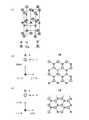
GaN系半導体はウルツ鉱型結晶構造を有している。図1は、ウルツ鉱型結晶構造の面を4指数表記(六方晶指数)で示している。4指数表記では、a1、a2、a3およびcで示される基本ベクトルを用いて結晶面や方位が表される。基本ベクトルcは、[0001]方向に延びており、この方向は「c軸」と呼ばれる。c軸に垂直な面(plane)は「c面」または「(0001)面」と呼ばれている。なお、「c軸」および「c面」は、それぞれ、「C軸」および「C面」と表記される場合もある。図2(a)はGaN系半導体の結晶構造を棒球モデルで示しており、図2(b)は、c軸に垂直な平面におけるGaN系半導体結晶のGaおよびNの位置を示している。 The GaN-based semiconductor has a wurtzite crystal structure. FIG. 1 shows the surface of the wurtzite crystal structure in four-index notation (hexagonal crystal index). In the 4-index notation, crystal planes and orientations are expressed using basic vectors represented by a1, a2, a3, and c. The basic vector c extends in the [0001] direction, and this direction is called “c-axis”. A plane perpendicular to the c-axis is called “c-plane” or “(0001) plane”. Note that “c-axis” and “c-plane” may be referred to as “C-axis” and “C-plane”, respectively. FIG. 2A shows the crystal structure of the GaN-based semiconductor by a rod-and-ball model, and FIG. 2B shows the positions of Ga and N of the GaN-based semiconductor crystal in a plane perpendicular to the c-axis.
従来、GaN系半導体を用いて半導体素子を作製する場合、GaN系半導体結晶を成長させる基板として、c面基板すなわち(0001)面を表面に有する基板が使用される。この場合、図2(a)および(b)から分かるように、c軸方向にはGa原子のみが配置される層と、N原子のみが配置される層が形成される。このようなGa原子およびN原子の配置に起因して、GaN系半導体には自発的な分極(Electrical Polarization)が形成される。このため、「c面」は「極性面」とも呼ばれている。 Conventionally, when a semiconductor element is manufactured using a GaN-based semiconductor, a c-plane substrate, that is, a substrate having a (0001) plane on the surface is used as a substrate on which a GaN-based semiconductor crystal is grown. In this case, as can be seen from FIGS. 2A and 2B, a layer in which only Ga atoms are arranged and a layer in which only N atoms are arranged are formed in the c-axis direction. Due to the arrangement of Ga atoms and N atoms, spontaneous polarization (electrical polarization) is formed in the GaN-based semiconductor. For this reason, the “c-plane” is also called “polar plane”.
その結果、GaN系半導体発光素子の活性層におけるInGaNの量子井戸には、c軸方向に沿ってピエゾ電界が発生し、活性層内における電子およびホールの分布に位置ずれが生じるため、キャリアの量子閉じ込めシュタルク効果により、活性層の内部量子効率が低下する。半導体レーザの場合、しきい値電流の増大が生じ、LEDの場合、消費電力の増大や発光効率の低下が生じる。また、注入キャリア密度の上昇と共にピエゾ電界のスクリーニングが起こり、発光波長の変化も生じる。 As a result, a piezoelectric electric field is generated along the c-axis direction in the InGaN quantum well in the active layer of the GaN-based semiconductor light-emitting device, and displacement of electrons and holes in the active layer is displaced. Due to the confined Stark effect, the internal quantum efficiency of the active layer is reduced. In the case of a semiconductor laser, the threshold current increases, and in the case of an LED, the power consumption increases and the light emission efficiency decreases. In addition, the piezo electric field is screened as the injected carrier density is increased, and the emission wavelength is also changed.
また、緑色やオレンジ色、さらには赤色など長波長域の光を発光させるために、InGaN活性層のIn組成を増加すると、In組成と共にピエゾ電界の強度は益々増加し、内部量子効率は急激に低下する。このため、一般にc面のInGaN活性層を用いたLEDでは、発光可能な光の波長は550nm程度であると言われている。 In addition, when the In composition of the InGaN active layer is increased to emit light in the long wavelength region such as green, orange, and even red, the intensity of the piezo electric field increases with the In composition, and the internal quantum efficiency rapidly increases. descend. For this reason, it is generally said that in an LED using a c-plane InGaN active layer, the wavelength of light that can be emitted is about 550 nm.
このような課題を解決するため、非極性面であるm面を表面に有する基板(m面GaN系基板)を使用して、発光素子を製造することが検討されている。図1に示すように、ウルツ鉱型結晶構造におけるm面は、c軸に平行であり、c面と直交する6つの等価な面である。例えば、図1においてハッチングで示された[10−10]方向に垂直な(10−10)面である。(10−10)面と等価な他のm面には、(−1010)面、(1−100)面、(−1100)面、(01−10)面、(0−110)面がある。ここで、ミラー指数を表すカッコ内の数字の左に付された「−」は、「バー」を意味する。 In order to solve such problems, it has been studied to manufacture a light-emitting element using a substrate (m-plane GaN-based substrate) having a non-polar m-plane on the surface. As shown in FIG. 1, the m-plane in the wurtzite crystal structure is six equivalent planes that are parallel to the c-axis and orthogonal to the c-plane. For example, the (10-10) plane perpendicular to the [10-10] direction indicated by hatching in FIG. Other m planes equivalent to the (10-10) plane include (-1010) plane, (1-100) plane, (-1100) plane, (01-10) plane, and (0-110) plane. . Here, “-” added to the left of the number in parentheses representing the Miller index means “bar”.
図2(c)は、m面に垂直な面におけるGaN系半導体結晶のGaおよびNの位置を示している。図2(c)に示すように、m面においては、Ga原子および窒素原子は同一原子面上に存在するため、m面に垂直な方向に分極は発生しない。このため、m面上に形成した半導体積層構造を用いて発光素子を作製すれば、活性層にピエゾ電界が発生せず、上述の課題を解決することができる。 FIG. 2C shows the positions of Ga and N of the GaN-based semiconductor crystal in a plane perpendicular to the m-plane. As shown in FIG. 2C, in the m plane, Ga atoms and nitrogen atoms are present on the same atomic plane, so that no polarization occurs in a direction perpendicular to the m plane. For this reason, when a light emitting element is manufactured using a semiconductor multilayer structure formed on the m-plane, a piezoelectric field is not generated in the active layer, and the above-described problems can be solved.
また、活性層のIn組成を大きく増加させることが可能であるため、青色のみならず、緑色や、オレンジ色、赤色など、より長波長の光を発光することのできるLEDやレーザダイオードを同一の材料系を用いて実現することができる。 In addition, since the In composition of the active layer can be greatly increased, the same LED or laser diode that can emit longer wavelength light such as green, orange, and red as well as blue is used. It can be realized using a material system.
なお、本明細書では、六方晶ウルツ鉱構造のX面(X=c、m)に垂直な方向にエピタキシャル成長が生じることを「X面成長」と表現する。X面成長において、X面を「成長面」と称し、X面成長によって形成された半導体の層を「X面半導体層」と称する。 In this specification, the occurrence of epitaxial growth in the direction perpendicular to the X plane (X = c, m) of the hexagonal wurtzite structure is expressed as “X plane growth”. In the X plane growth, the X plane is referred to as a “growth plane”, and a semiconductor layer formed by the X plane growth is referred to as an “X plane semiconductor layer”.
さらに、非特許文献1などに開示されているように、m面上に形成されたInGaN活性層を用いたLEDは、その価電子帯の構造に由来した偏光特性を有している。具体的にはa軸に平行な方向に偏光した光を出射する。 Further, as disclosed in
このため、偏光特性を有する光を出射することが可能な発光素子として利用することが期待される。例えば、液晶表示装置は、液晶の偏光方向を制御する働きを利用するため、光源として、偏光した光を用いる必要がある。従来の液晶表示装置では、偏光特性を有する光を出射する適切な光源がないため、LEDやCCFL蛍光管などの光源を用い、偏光板に出射した光を通過させることによって、偏光特性を有する光を得ていた。しかし、この様な構成によれば、光源から出射する光の大部分は偏光板で遮られるため、光の利用効率が低いという問題があった。したがって、m面上に形成されたInGaN活性層を用いたLEDを液晶表示装置の光源として使用すれば、光の利用効率が向上し、液晶表示装置の消費電力を大幅に低減したり、偏光板を設けなくてよいことから、製造コストを低減したりすることも可能となる。 For this reason, it is expected to be used as a light emitting element capable of emitting light having polarization characteristics. For example, since a liquid crystal display device uses a function of controlling the polarization direction of liquid crystal, it is necessary to use polarized light as a light source. In a conventional liquid crystal display device, since there is no appropriate light source that emits light having polarization characteristics, light having polarization characteristics is obtained by using a light source such as an LED or a CCFL fluorescent tube to pass the light emitted to the polarizing plate. Was getting. However, according to such a configuration, since most of the light emitted from the light source is blocked by the polarizing plate, there is a problem that the light use efficiency is low. Therefore, if an LED using an InGaN active layer formed on the m-plane is used as a light source of a liquid crystal display device, the light utilization efficiency is improved, and the power consumption of the liquid crystal display device is greatly reduced. Therefore, it is possible to reduce the manufacturing cost.
上述したように、m面基板上で成長させたGaN系半導体素子は、c面基板上で成長させたものと比較して顕著な効果を発揮し得る。しかし、m面基板上で成長させたGaN系半導体素子は、c面基板上で成長させたものよりも機械的強度が低いという課題がある。このことは、m面基板上で成長させたGaN系半導体素子を実用化する上で技術的な障害となっている。 As described above, the GaN-based semiconductor element grown on the m-plane substrate can exhibit a remarkable effect as compared with that grown on the c-plane substrate. However, a GaN-based semiconductor element grown on an m-plane substrate has a problem that its mechanical strength is lower than that grown on a c-plane substrate. This is a technical obstacle in putting a GaN-based semiconductor element grown on an m-plane substrate into practical use.
本発明はかかる点に鑑みてなされたものであり、その主な目的は、偏光特性に優れ、面基板上で結晶成長させたGaN系半導体素子における物理的強度を高めることのできる構造およびそれを用いた照明装置および液晶表示装置を提供することにある。 The present invention has been made in view of the above points, and its main purpose is to provide a structure capable of enhancing the physical strength of a GaN-based semiconductor element having excellent polarization characteristics and crystal growth on a surface substrate, and the structure thereof. An object of the present invention is to provide a lighting device and a liquid crystal display device used.
本発明の照明装置は、少なくとも第1および第2の窒化物系半導体発光素子を備えた照明装置であって、前記第1および第2の窒化物系半導体発光素子のそれぞれは半導体チップを備え、前記半導体チップは、AlxInyGazN(x+y+z=1、x≧0、y≧0、z≧0)半導体から形成された窒化物系半導体積層構造を含み、前記窒化物系半導体積層構造は、窒化物半導体層からなる活性層領域を含み、前記活性層領域は、m面から1°以上の角度で傾斜しており、前記活性層領域における主面の法線とm面の法線とが形成する角度が1°以上5°以下であり、前記第1および第2の窒化物系半導体発光素子は、それぞれ前記活性層領域から偏光を出射し、前記第1および第2の窒化物系半導体発光素子が出射する偏光の波長をそれぞれλ1およびλ2とし、前記第1および第2の窒化物系半導体発光素子の半導体チップの厚さをそれぞれd1およびd2としたとき、λ1<λ2かつd1<d2の関係を満たしている。The illumination device of the present invention is an illumination device including at least first and second nitride-based semiconductor light-emitting elements, each of the first and second nitride-based semiconductor light-emitting elements including a semiconductor chip, the semiconductor chipis, Al x in y Ga z N (x + y + z = 1, x ≧ 0, y ≧ 0, z ≧ 0) includes a nitride-based semiconductor multilayer structure formed from a semiconductor, the nitride-based semiconductor multilayer structure Includes an active layer region made of a nitride semiconductor layer, and the active layer region is inclined at an angle of 1 ° or more from the m-plane, and the normal of the main surface and the normal of the m-plane in the active layer region And the first and second nitride-based semiconductor light emitting devices emit polarized light from the active layer region, respectively, and the first and second nitrides are formed. The wavelength of the polarized light emitted by the semiconductor light emitting device And .lambda.1 and .lambda.2, when the thickness of the semiconductor chip of the first and second nitride-based semiconductor light-emitting device was respectively d1 and d2, it satisfies the relationship of .lambda.1 <.lambda.2 and d1 <d2.
ある好ましい実施形態において、前記活性層領域は、c軸方向またはa軸方向に傾斜している。 In a preferred embodiment, the active layer region is inclined in the c-axis direction or the a-axis direction.
ある好ましい実施形態において、照明装置は、前記半導体チップを備えた第3の窒化物系半導体発光素子をさらに備え、前記第3の窒化物系半導体発光素子が出射する偏光の波長をλ3とし、前記第3の窒化物系半導体発光素子の半導体チップの厚さをd3としたとき、λ1<λ2<λ3かつd1<d2<d3の関係を満たしている。 In a preferred embodiment, the lighting device further includes a third nitride-based semiconductor light-emitting element including the semiconductor chip, and a wavelength of polarized light emitted from the third nitride-based semiconductor light-emitting element is λ3, When the thickness of the semiconductor chip of the third nitride semiconductor light emitting device is d3, the relationship of λ1 <λ2 <λ3 and d1 <d2 <d3 is satisfied.
ある好ましい実施形態において、前記第1の窒化物半導体発光素子、前記第2の窒化物半導体発光素子、及び前記第3の窒化物系半導体発光素子が出射する偏光の偏光方向が、同一方向に揃っている。 In a preferred embodiment, polarization directions of polarized light emitted from the first nitride semiconductor light emitting device, the second nitride semiconductor light emitting device, and the third nitride semiconductor light emitting device are aligned in the same direction. ing.
ある好ましい実施形態において、照明装置は支持基板をさらに有し、前記第1、第2および第3の窒化物系半導体発光素子は前記支持基板上に支持されている。 In a preferred embodiment, the lighting device further includes a support substrate, and the first, second, and third nitride-based semiconductor light-emitting elements are supported on the support substrate.
ある好ましい実施形態において、前記λ1、λ2およびλ3は、それぞれ青色領域、緑色領域および赤色領域の波長である。 In a preferred embodiment, λ1, λ2, and λ3 are wavelengths of a blue region, a green region, and a red region, respectively.
ある好ましい実施形態において、前記λ1、λ2およびλ3は、それぞれ、420nm以上470nm以下、520nm以上560nm以下および590nm以上660nm以下である。 In one preferable embodiment, λ1, λ2, and λ3 are 420 nm or more and 470 nm or less, 520 nm or more and 560 nm or less, and 590 nm or more and 660 nm or less, respectively.
ある好ましい実施形態において、前記d1、d2およびd3は、それぞれ、110μm以上150μm以下、200μm以上240μm以下および250μm以上290μmである。 In a preferred embodiment, the d1, d2, and d3 are 110 μm or more and 150 μm or less, 200 μm or more and 240 μm or less, and 250 μm or more and 290 μm, respectively.
ある好ましい実施形態において、照明装置は、AlGaInP系発光素子と、前記AlGaInP系発光素子から出射する光が透過する位置に設けられた偏光フィルタとをさらに備え、前記λ1およびλ2は、それぞれ青色領域および緑色領域の波長である。 In a preferred embodiment, the illumination device further includes an AlGaInP-based light emitting element and a polarizing filter provided at a position where light emitted from the AlGaInP-based light emitting element is transmitted, wherein λ1 and λ2 are a blue region and λ2, respectively. The wavelength in the green region.
ある好ましい実施形態において、前記d1およびd2は、それぞれ、110μm以上150μm以下および200μm以上240μm以下である。 In a preferred embodiment, d1 and d2 are 110 μm or more and 150 μm or less and 200 μm or more and 240 μm or less, respectively.
ある好ましい実施形態において、前記λ1およびλ2は、それぞれ、420nm以上470nm以下および520nm以上560nm以下である。 In a preferred embodiment, λ1 and λ2 are 420 nm or more and 470 nm or less and 520 nm or more and 560 nm or less, respectively.
ある好ましい実施形態において、前記第1および第2の窒化物系半導体発光素子のそれぞれは、前記窒化物系半導体積層構造の一部に設けられた、MgまたはMg合金から形成されたp型電極を有する。 In a preferred embodiment, each of the first and second nitride-based semiconductor light-emitting elements includes a p-type electrode formed of Mg or Mg alloy provided in a part of the nitride-based semiconductor multilayer structure. Have.
ある好ましい実施形態において、照明装置は、前記第1および第2の窒化物系半導体発光素子から出射する偏光をそれぞれ集光する一対の光学レンズをさらに備える。 In a preferred embodiment, the illuminating device further includes a pair of optical lenses that respectively collect the polarized light emitted from the first and second nitride-based semiconductor light emitting elements.
ある好ましい実施形態において、照明装置は、前記第1および第2の窒化物系半導体発光素子から出射する偏光を共通に集光する光学レンズをさらに備える。 In a preferred embodiment, the illumination device further includes an optical lens that condenses the polarized light emitted from the first and second nitride-based semiconductor light emitting elements in common.
ある好ましい実施形態において、前記光学レンズは、前記窒化物系半導体発光素子から出射した光を平行光に変換する。 In a preferred embodiment, the optical lens converts light emitted from the nitride-based semiconductor light-emitting element into parallel light.
ある好ましい実施形態において、前記光学レンズの焦点位置近傍に、前記第1の窒化物系半導体発光素子および前記第2の窒化物系半導体発光素子の発光面が配置されている。 In a preferred embodiment, light emitting surfaces of the first nitride semiconductor light emitting device and the second nitride semiconductor light emitting device are disposed in the vicinity of the focal position of the optical lens.
ある好ましい実施形態において、照明装置は、光学シートと、光学板とをさらに備える。 In a preferred embodiment, the lighting device further includes an optical sheet and an optical plate.
本発明の液晶表示装置は、液晶パネルと、上記照明装置とを備える。 The liquid crystal display device of the present invention includes a liquid crystal panel and the illumination device.
本発明の窒化物系半導体発光素子は、半導体チップを備えた窒化物系半導体発光素子であって、前記半導体チップは、AlxInyGazN(x+y+z=1、x≧0、y≧0、z≧0)半導体から形成された窒化物系半導体積層構造を含み、前記窒化物系半導体積層構造は、窒化物半導体層からなる活性層領域を有しており、前記活性層領域は、m面から1°以上の角度で傾斜しており、前記活性層領域における主面の法線とm面の法線とが形成する角度が1°以上5°以下であり、前記活性層領域から420nm以上470nm以下の波長の偏光を出射し、前記半導体チップの厚さが110μm以上150μm以下である。Nitride-based semiconductor light-emitting device of the present invention is the nitride-based semiconductor light-emitting device comprising a semiconductor chip, the semiconductorchip, Al x In y Ga z N (x + y + z = 1, x ≧ 0, y ≧ 0 , Z ≧ 0) including a nitride-based semiconductor multilayer structure formed of a semiconductor, and the nitride-based semiconductor multilayer structure has an active layer region made of a nitride semiconductor layer, and the active layer region is m It is inclined at an angle of 1 ° or more from the surface, and the angle formed by the normal of the main surface and the normal of the m-plane in the active layer region is 1 ° or more and 5 ° or less, and 420 nm from the active layer region. The polarized light having a wavelength of 470 nm or less is emitted, and the thickness of the semiconductor chip is 110 μm or more and 150 μm or less.
本発明の窒化物系半導体発光素子は、半導体チップを備えた窒化物系半導体発光素子であって、前記半導体チップは、AlxInyGazN(x+y+z=1、x≧0、y≧0、z≧0)半導体から形成された窒化物系半導体積層構造を含み、前記窒化物系半導体積層構造は、窒化物半導体層からなる活性層領域を有しており、前記活性層領域は、m面から1°以上の角度で傾斜しており、前記活性層領域における主面の法線とm面の法線とが形成する角度が1°以上5°以下であり、前記活性層領域から520nm以上560nm以下の波長の偏光を出射し、前記半導体チップの厚さが200μm以上240μm以下である。Nitride-based semiconductor light-emitting device of the present invention is the nitride-based semiconductor light-emitting device comprising a semiconductor chip, the semiconductorchip, Al x In y Ga z N (x + y + z = 1, x ≧ 0, y ≧ 0 , Z ≧ 0) including a nitride-based semiconductor multilayer structure formed of a semiconductor, and the nitride-based semiconductor multilayer structure has an active layer region made of a nitride semiconductor layer, and the active layer region is m It is inclined at an angle of 1 ° or more from the surface, and the angle formed by the normal of the main surface and the normal of the m-plane in the active layer region is 1 ° or more and 5 ° or less, and 520 nm from the active layer region. The polarized light having a wavelength of 560 nm or less is emitted, and the thickness of the semiconductor chip is 200 μm or more and 240 μm or less.
本発明の窒化物系半導体発光素子は、半導体チップを備えた窒化物系半導体発光素子であって前記半導体チップは、AlxInyGazN(x+y+z=1、x≧0、y≧0、z≧0)半導体から形成された窒化物系半導体積層構造を含み、前記窒化物系半導体積層構造は、窒化物半導体層からなる活性層領域を有しており、前記活性層領域は、m面から1°以上の角度で傾斜しており、前記活性層領域における主面の法線とm面の法線とが形成する角度が1°以上5°以下であり、前記活性層領域から590nm以上660nm以下の波長の偏光を出射し、前記半導体チップの厚さが250μm以上290μm以下である。Nitride-based semiconductor light-emitting device of the present invention, the semiconductor chip to a nitride-based semiconductor light-emitting device comprising a semiconductorchip, Al x In y Ga z N (x + y + z = 1, x ≧ 0, y ≧ 0, z ≧ 0) including a nitride-based semiconductor multilayer structure formed of a semiconductor, wherein the nitride-based semiconductor multilayer structure has an active layer region made of a nitride semiconductor layer, and the active layer region has an m-plane And an angle formed by the normal of the main surface and the normal of the m-plane in the active layer region is 1 ° or more and 5 ° or less, and 590 nm or more from the active layer region. Polarized light having a wavelength of 660 nm or less is emitted, and the thickness of the semiconductor chip is 250 μm or more and 290 μm or less.
本発明の少なくとも第1および第2の窒化物系半導体発光素子を備えた照明装置の製造方法は、基板を用意する工程(a)と、m面窒化物半導体層からなる活性層領域を有しており、AlxInyGazN(x+y+z=1、x≧0、y≧0、z≧0)半導体から形成された窒化物系半導体積層構造を前記基板上に形成する工程であって、前記活性層領域を、m面から1°以上の角度で傾斜させ、前記活性層領域における主面の法線とm面の法線とが形成する角度が1°以上5°以下である前記窒化物系半導体積層構造を前記基板上に形成する工程(b)と、前記窒化物系半導体積層構造に電極を形成し、前記活性層領域から偏光を出射する半導体チップを作製する工程(c)と、前記活性層領域から出射する偏光の波長に応じた厚さとなるように、前記半導体チップの厚さを調整する工程(d)とを含み、発光波長および半導体チップの厚さがそれぞれ互いに異なる第1および第2の窒化物系半導体発光素子を作製する工程(A)と、前記第1および第2の窒化物系半導体発光素子を支持基板上に配置する工程(B)とを包含し、前記工程(A)の前記工程(d)において、前記第1および第2の窒化物系半導体発光素子が出射する偏光の波長をそれぞれλ1およびλ2とし、前記第1および第2の窒化物系半導体発光素子の半導体チップの厚さをそれぞれd1およびd2としたとき、λ1<λ2かつd1<d2の関係を満たすように、前記第1および第2の窒化物系半導体発光素子の前記半導体チップの厚さをそれぞれ調整する。The manufacturing method of the illuminating device provided with the 1st and 2nd nitride semiconductor light emitting element of this invention of this invention has the process (a) which prepares a board | substrate, and the active layer area | region which consists of an m-plane nitride semiconductor layer. and is, anAl x in y Ga z N ( x + y + z = 1, x ≧ 0, y ≧ 0, z ≧ 0) step of a nitride-based semiconductor multilayer structure formed from a semiconductor is formed on the substrate, The nitridation in which the active layer region is inclined at an angle of 1 ° or more from the m-plane, and an angle formed by a normal of the main surface and the normal of the m-plane in the active layer region is 1 ° or more and 5 ° or less A step (b) of forming a physical semiconductor multilayer structure on the substrate; a step (c) of forming an electrode on the nitride semiconductor multilayer structure and producing a semiconductor chip that emits polarized light from the active layer region; The thickness will be in accordance with the wavelength of polarized light emitted from the active layer region. The step (d) of adjusting the thickness of the semiconductor chip, and the step (A) of fabricating first and second nitride-based semiconductor light-emitting elements having different emission wavelengths and semiconductor chip thicknesses, respectively. And the step (B) of disposing the first and second nitride-based semiconductor light-emitting elements on a support substrate. In the step (d) of the step (A), the first and second steps When the wavelengths of polarized light emitted from the nitride-based semiconductor light-emitting element are λ1 and λ2, respectively, and the thicknesses of the semiconductor chips of the first and second nitride-based semiconductor light-emitting elements are d1 and d2, respectively, λ1 < The thicknesses of the semiconductor chips of the first and second nitride-based semiconductor light emitting devices are adjusted so as to satisfy the relationship of λ2 and d1 <d2.
ある好ましい実施形態において前記第1の窒化物半導体発光素子及び前記第2の窒化物系半導体発光素子が出射する偏光の偏光方向が、同一方向に揃うように、前記支持基板上に配置する。 In a preferred embodiment, the first nitride semiconductor light emitting device and the second nitride semiconductor light emitting device are arranged on the support substrate so that polarization directions of polarized light emitted from the first nitride semiconductor light emitting device are aligned in the same direction.
本発明の窒化物系半導体発光素子によれば、主面の法線とm面の法線とが形成する角度が1°以上5°以下の活性層領域を備えており、発光波長に応じて、半導体チップの厚さが所定の厚さに設定されているため、偏光特性に優れた光を出射することができ、また、半導体チップの機械的強度を高めることができる。 According to the nitride-based semiconductor light-emitting device of the present invention, the active layer region having an angle formed by the normal of the main surface and the normal of the m-plane of 1 ° or more and 5 ° or less is provided depending on the emission wavelength. Since the thickness of the semiconductor chip is set to a predetermined thickness, light with excellent polarization characteristics can be emitted, and the mechanical strength of the semiconductor chip can be increased.
また、本発明の照明装置によれば、2つ以上の窒化物系半導体発光素子を備え、2つ窒化物系半導体発光素子100の発光波長をλ1およびλ2とし、半導体チップの厚さd1およびd2としたとき、をλ1<λ2およびd1<d2の関係を満たしている。このため、偏光特性に優れた光を出射することができ、また、半導体チップの機械的強度を高めることができる。 In addition, according to the lighting device of the present invention, two or more nitride-based semiconductor light-emitting elements are provided, the emission wavelengths of the two nitride-based semiconductor light-emitting
このよう照明装置を用いることにより、偏光特性を有効利用した高効率で低コストな液晶表示装置が実現する。 By using such an illuminating device, a highly efficient and low-cost liquid crystal display device that effectively utilizes polarization characteristics is realized.
本願発明者は、m面上に形成したGaN系発光素子の偏光特性および機械的強度について詳細な検討を行った。その結果、偏光特性および機械的強度は、GaN系発光素子を構成する半導体チップの厚さおよび活性層から出射する光の波長に依存することを見出した。この知見に基づき、本願発明者は、m面上に形成したGaN系発光素子において、半導体チップの厚さを最適化することによって、m面上に形成した半導体積層構造を有し、偏光特性に優れ、かつ、十分な機械的強度を備えたGaN系発光素子を創案した。以下、図面を参照しながら、本発明の実施形態を説明する。 The inventor of the present application has conducted detailed studies on the polarization characteristics and mechanical strength of the GaN-based light emitting device formed on the m-plane. As a result, it has been found that the polarization characteristics and the mechanical strength depend on the thickness of the semiconductor chip constituting the GaN-based light emitting device and the wavelength of light emitted from the active layer. Based on this knowledge, the inventor of the present application has a semiconductor stacked structure formed on the m-plane by optimizing the thickness of the semiconductor chip in the GaN-based light emitting device formed on the m-plane, and has polarization characteristics. A GaN-based light emitting device with excellent mechanical strength was created. Hereinafter, embodiments of the present invention will be described with reference to the drawings.
(第1の実施形態)
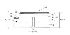
以下、図面を参照しながら、本発明による窒化物系半導体発光素子および照明装置の実施形態を説明する。図3は、本発明の一実施形態である窒化物系半導体発光素子100の断面構造を模式的に示している。図3に示す窒化物系半導体発光素子100は、半導体チップ45によって構成されている。(First embodiment)
Embodiments of a nitride-based semiconductor light-emitting element and a lighting device according to the present invention will be described below with reference to the drawings. FIG. 3 schematically shows a cross-sectional structure of a nitride-based semiconductor light-emitting
半導体チップ45は、基板10と、基板10上においてエピタキシャル成長した窒化物系半導体積層構造20を含む。窒化物系半導体積層構造20は、GaN系半導体、より具体的には、AlxInyGazN(x+y+z=1、x≧0、y≧0、z≧0)半導体から形成されている。また、窒化物系半導体積層構造20は発光領域として機能する活性層領域24を含んでいる。The
本発明では、偏光特性に優れ、高い発光効率で発光する発光素子を実現するため、m面上に形成された、窒化物半導体層からなる活性層領域を用いる。この活性層領域は、m面に対して成長方向が垂直であり(m面窒化物半導体層)、m面に平行でもある。このために、窒化物系半導体発光素子100において、活性層領域24を含む窒化物系半導体積層構造20はm面を表面12とするGaN系半導体からなる基板10上に形成されている。ただし、r面サファイア基板上にa面GaNが成長するという事例もあることから、窒化物系半導体積層構造20の活性層領域24がm面と平行な結晶方位を有する、すなわち活性層領域の成長方向がm軸方向である限り、基板10の表面12は必ずしもm面でなくてもよい。 In the present invention, an active layer region made of a nitride semiconductor layer formed on the m-plane is used in order to realize a light-emitting element that has excellent polarization characteristics and emits light with high luminous efficiency. This active layer region has a growth direction perpendicular to the m-plane (m-plane nitride semiconductor layer) and is also parallel to the m-plane. For this reason, in the nitride semiconductor
実際のm面半導体層の表面(主面)は、m面に対して完全に平行な面である必要は無く、m面から僅かな角度(0度より大きく±1°未満)で傾斜していても良い。表面がm面に対して完全に平行な表面を有する基板や半導体層を形成することは、製造技術の観点から困難である。このため、現在の製造技術によってm面基板やm面半導体層を形成した場合、現実の表面は理想的なm面から傾斜してしまう。傾斜の角度および方位は、製造工程によってばらつくため、表面の傾斜角度および傾斜方位を正確に制御することは難しい。 The actual surface (main surface) of the m-plane semiconductor layer does not need to be a plane that is completely parallel to the m-plane, and is inclined at a slight angle (greater than 0 ° and less than ± 1 °) from the m-plane. May be. It is difficult to form a substrate or a semiconductor layer having a surface that is completely parallel to the m-plane from the viewpoint of manufacturing technology. For this reason, when an m-plane substrate or an m-plane semiconductor layer is formed by the current manufacturing technology, the actual surface is inclined from the ideal m-plane. Since the inclination angle and orientation vary depending on the manufacturing process, it is difficult to accurately control the inclination angle and inclination orientation of the surface.
なお、基板や半導体の表面(主面)をm面から1°以上の角度で傾斜させることを意図的に行う場合がある。以下に説明する第4の実施形態では、活性層領域24の表面(主面)をm面から1°以上の角度で意図的に傾斜させている。 In some cases, the surface (main surface) of the substrate or semiconductor is intentionally inclined at an angle of 1 ° or more from the m-plane. In the fourth embodiment described below, the surface (main surface) of the
窒化物半導体積層構造20は、活性層領域24を挟むように配置された第1導電型の半導体層22および第2導電型の半導体層26を含んでいる。本実施形態では、第1導電型の半導体層22が活性層領域24に対して基板10側に位置しており、第2導電型の半導体層26は基板10と反対側に位置している。活性層領域24と第2導電型の半導体層26との間に、アンドープのGaN層を設けてもよい。 The nitride
第1導電型の半導体層22は、例えば、n型のAluGavInwN(u+v+w=1、u≧0、v≧0、w≧0)から形成されている。n型ドーパントとして例えば、シリコン(Si)を用いることができる。The first conductivity type semiconductor layer 22 is formed of, for example, n-type Alu Gav Inw N (u + v + w = 1, u ≧ 0, v ≧ 0, w ≧ 0). For example, silicon (Si) can be used as the n-type dopant.
第2導電型の半導体層26は、例えば、p型のAlsGatN(s+t=1、s≧0、t≧0)半導体からなる。ドーパントとして例えばMgが添加されている。Mg以外のp型ドーパントとして、例えばZn、Beなどを用いてもよい。第2導電型の半導体層26において、Alの組成比率sは、厚さ方向に一様であってもよいし、Alの組成比率sが厚さ方向に連続的または階段的に変化していてもよい。具体的には、第2導電型の半導体層26は、Alの組成比率sが異なる複数の副層が積層された多層構造を有していてもよいし、ドーパントの濃度も厚さ方向に変化していてもよい。第2導電型の半導体層26の厚さは、例えば、0.2〜2μmである。The semiconductor layer 26 of the second conductivity type, forexample, Al s Ga t N (s + t = 1, s ≧ 0, t ≧ 0) of p-type of semiconductor. For example, Mg is added as a dopant. As a p-type dopant other than Mg, for example, Zn or Be may be used. In the second conductivity type semiconductor layer 26, the Al composition ratio s may be uniform in the thickness direction, or the Al composition ratio s may vary continuously or stepwise in the thickness direction. Also good. Specifically, the second conductivity type semiconductor layer 26 may have a multilayer structure in which a plurality of sub-layers having different Al composition ratios s are stacked, and the dopant concentration also changes in the thickness direction. You may do it. The thickness of the second conductivity type semiconductor layer 26 is, for example, 0.2 to 2 μm.
第2導電型の半導体層26の上面が窒化物半導体積層構造20の上面となる場合には、コンタクト抵抗低減の観点から、第2導電型の半導体層26の上面近傍はAlの組成比率sがゼロである半導体、つまり、GaNから形成されていることが好ましい。また、この場合、GaNは第2導電型の不純物が高濃度で含まれており、コンタクト層として機能することが好ましい。 When the upper surface of the second conductivity type semiconductor layer 26 becomes the upper surface of the nitride
あるいは、窒化物半導体積層構造20は第2導電型の半導体層26の上に、第2導電型のGaN層を含んでいてもよい。また、窒化物半導体積層構造20は第2導電型のGaN層上にさらにp+−GaNからなるコンタクト層を含んでいてもよい。Alternatively, the nitride
活性層領域24は、窒化物系半導体発光素子100における電子注入領域である。活性層領域24は、例えば、Ga1-xInxN井戸層(0.14≦x≦0.45)(例えば、厚さ9nm)とGaNバリア層(例えば、厚さ9nm)とが交互に積層されたGaInN/GaN多重量子井戸(MQW)構造(例えば、厚さ81nm)を有している。窒化物系半導体発光素子100から出射する光の波長は、活性層領域24を構成する半導体のバンドギャップの大きさ、より具体的には、井戸層の半導体組成であるGa1-xInxN半導体におけるInの組成xによって決まる。m面上に形成された活性層領域24にはピエゾ電界が発生しない。このため、In組成を増加させても発光効率の低下が抑制される。その結果、窒化物系半導体を用いた発光素子であってもIn組成を大きく増加することにより、赤色の発光ダイオードやレーザダイオードを実現することができる。また、m面上に形成された活性層領域24を用いることによって、a軸と平行な方向に偏光した光を発光させることができる。The
青色領域の光の波長λ1は420nm以上470nm以下であり、青色領域の光を発光させるためには、Inの組成xは例えば0.14≦x≦0.22を満たす値に設定する。同様に、緑色領域の光の波長λ2は520nm以上560nm以下であり、緑色領域の光を発光させるためには、Inの組成xは例えば0.29≦x≦0.34を満たす値に設定する。赤色領域の光の波長λ3は590nm以上660nm以下であり、赤色領域の光を発光させるためには、Inの組成xは例えば0.38≦x≦0.45を満たす値に設定する。より具体的には、例えば発光波長が450nmの青色であればx=0.18〜0.2であり、520nmの緑色であればx=0.29〜0.31であり、630nmの赤色であればx=0.43〜0.44である。なお、発光波長は井戸層厚、歪量、製造方法などに依存するため、発光波長に対応するInの組成は、上述した範囲から多少ずれることもある。本実施形態の窒化物系半導体発光素子100では、これらの波長の光のいずれもがa軸と平行な方向に偏光している。 The wavelength λ1 of light in the blue region is not less than 420 nm and not more than 470 nm. In order to emit light in the blue region, the In composition x is set to a value satisfying, for example, 0.14 ≦ x ≦ 0.22. Similarly, the wavelength λ2 of light in the green region is not less than 520 nm and not more than 560 nm, and in order to emit light in the green region, the In composition x is set to a value satisfying 0.29 ≦ x ≦ 0.34, for example. . The wavelength λ3 of light in the red region is not less than 590 nm and not more than 660 nm. In order to emit light in the red region, the In composition x is set to a value satisfying, for example, 0.38 ≦ x ≦ 0.45. More specifically, for example, if the emission wavelength is 450 nm in blue, x = 0.18 to 0.2, and if it is 520 nm in green, x = 0.29 to 0.31, and 630 nm in red. If present, x = 0.43 to 0.44. Since the emission wavelength depends on the thickness of the well layer, the amount of strain, the manufacturing method, and the like, the composition of In corresponding to the emission wavelength may slightly deviate from the above range. In the nitride semiconductor
窒化物系半導体発光素子100は、第1導電型の半導体層22および第2導電型の半導体層26にそれぞれ低抵抗で接続された第1導電型電極40および第2導電型電極30をさらに備えている。本実施形態では、半導体積層構造20に凹部42を設けることによって、第1導電型の半導体層22の一部を露出させ、露出した第1導電型の半導体層22上に第1導電型電極40が設けられている。第1導電型電極40は、例えば、Ti層およびPt層の積層構造(Ti/Pt)を有し、第1導電型の半導体層22にオーミック接合している。これにより第1導電型電極40は、n型オーミック電極として機能する。 The nitride semiconductor
また、第2導電型の半導体層26上に第2導電型電極30が設けられている。第2導電型電極30は、好ましくは、第2導電型の半導体層26とオーミック接合している。第2導電型電極30は概ね第2導電型の半導体層26の表面全体を覆っていることが好ましい。これにより第2導電型電極30は、p型オーミック電極として機能する。第2導電型電極30はMgまたはMg合金からなることが好ましい。 A second
以上のように構成された窒化物系半導体発光素子100において、第1導電型電極40と第2導電型電極30との間に電圧を印加すると、第2導電型電極30から活性層領域24に向かって正孔が、第1導電型電極40から活性層領域24に向かって電子が注入される。活性層領域24において、正孔と電子とが再結合する際、活性層領域24の半導体組成によって定まるバンドギャップに応じた波長の光であって、a軸と平行な方向に偏光した光を活性層領域24から出射する。 In the nitride semiconductor
偏光特性に優れた光を出射し、かつ、高い機械的強度を備えるために、窒化物系半導体発光素子100は出射する光の波長に応じた半導体チップ45の厚さを有している。つまり、窒化物系半導体発光素子100において、活性層領域24を構成する半導体のバンドギャップが大きくなり、発光波長が長くなれば、それに応じて半導体チップ45も厚くなっている。 In order to emit light having excellent polarization characteristics and to have high mechanical strength, the nitride-based semiconductor
具体的には、窒化物系半導体発光素子100が青色領域の光(λ1=420nm〜470nm)を出射する場合、半導体チップ45の厚さd1は110μm以上150μm以下(130±20μm)である。同様にまた、窒化物系半導体発光素子100が緑色領域の光(λ2=520nm〜560nm)を出射する場合、半導体チップ45の厚さd2は200μm以上240μm以下(220±20μm)である。赤色領域の光(λ3=590nm〜660nm)を出射する場合には、半導体チップ45の厚さd3は250μm以上290μm以下(270±20μm)であることが好ましいと考えられる。半導体チップ45の厚さは、最も波長の短い光を出射させる場合でも110μm以上であり、この厚さは、一般的なc面窒化物系半導体発光素子のチップの厚さよりも大きい。 Specifically, when the nitride semiconductor
ここで半導体チップ45の厚さ(d1、d2、d3)とは、窒化物系半導体積層構造20の積層方向において、第1導電型電極40や第2導電型電極30を含む半導体チップ45全体の厚さを言う。ただし、第1導電型電極40や第2導電型電極30の厚さは数μm程度であり、また、窒化物系半導体積層構造20の厚さも数μm以下である。このため、半導体チップ45の厚さの大部分は基板10によって占められる。 Here, the thickness (
図4は、本発明による窒化物系半導体発光素子の照明装置の実施形態を示す模式的な断面図である。図4に示すように照明装置111は、支持基板50と支持基板上に支持された3つの窒化物系半導体発光素子100を備えている。窒化物系半導体発光素子100は上述した構造を備えており、例えば、第2導電型電極30が支持基板50側に位置するように、配置され、第1導電型電極40および第2導電型電極30が図示しないパッド電極などと例えばフリップチップボンディングなどで接合され、固定されている。3つの窒化物系半導体発光素子100から出射する光の偏光方向が一致するように、3つの窒化物系半導体発光素子100の方向が調整されている。例えば、3つの窒化物系半導体発光素子100の側面が互いに平行となるように配置すれば、3つの窒化物系半導体発光素子100からそれぞれ出射する光の偏光方向を互いに一致させることができる。 FIG. 4 is a schematic cross-sectional view showing an embodiment of an illumination device for a nitride-based semiconductor light-emitting element according to the present invention. As shown in FIG. 4, the
3つの窒化物系半導体発光素子100は、例えば、上述したようにそれぞれ青色領域の光(λ1)、緑色領域の光(λ2)および赤色領域の光(λ3)を出射するようにInの組成比が決定された活性層領域24を含んでいる。また、3つの窒化物系半導体発光素子100の半導体チップ45の厚さはそれぞれd1、d2、d3である。したがって、λ1<λ2<λ3であり、d1<d2<d3である。このように、発光波長が異なることによって半導体チップ45の厚さd1、d2、d3が互いに異なっており、発光波長が長くなるにつれて半導体チップ45の厚さが大きくなっていることが特徴である。 The three nitride-based semiconductor light-emitting
照明装置111は3つの窒化物系半導体発光素子100を備えているが、窒化物系半導体発光素子100は2つ以上であればよい。この場合、2つの窒化物系半導体発光素子100は、例えば、青色領域の光(λ1)および緑色領域の光(λ2)を出射するようにInの組成比が決定された活性層領域24を含んでいる。また、2つの窒化物系半導体発光素子100の半導体チップ45の厚さはそれぞれd1、d2である。したがって、λ1<λ2であり、d1<d2である。 The
照明装置111は、3つの窒化物系半導体発光素子100を同時に発光させることにより、一方向(a軸に平行な方向)に偏光した白色光を出射することができ、また、3つの窒化物系半導体発光素子100の発光強度を調節することによって、一方向(a軸に平行な方向)に偏光した任意の色の可視光を出射することができる。 The illuminating
以下、窒化物系半導体発光素子100および照明装置111における、半導体チップ45の厚さと偏光特性および半導体チップ45の機械的強度との関係を詳細に説明する。 Hereinafter, the relationship between the thickness of the
図5は、窒化物系半導体発光素子100の偏光特性を測定した結果を示す。図6は、測定に用いた構成を模式的に示している。窒化物系半導体発光素子100は実装基板62上にフリップチップ実装されており、窒化物系半導体発光素子100に電源61から電流を流すことにより発光が得られる。窒化物系半導体発光素子100から出射した光は偏光板63を通過し対物レンズ64によってカメラ65およびシリコンディテクター67の検出部66に導かれ、光の強度が検出される。窒化物系半導体発光素子100から出射する光が偏光特性を有する場合、偏光板63を回転することにより光の強度が変化することが観測される。 FIG. 5 shows the result of measuring the polarization characteristics of the nitride-based semiconductor
図5はシリコンディテクター67によって検出した光強度と偏光板63の回転角の関係を示す。m面に形成された活性層領域24のa軸に平行な方向に偏光した光を透過する偏光板の角度を0度として、偏光板63の角度を示している。図5に示すように、偏光板63を回転すると回転と共に光の検出強度が減少し、角度が90度の時、すなわちc軸に平行な方向に偏光した光を透過するように偏光板63が配置されたとき、光の検出強度は最小となった。このことから窒化物系半導体発光素子100から出射する光がa軸方向に偏光していることが確認できた。これに対し、c面の窒化物系半導体発光素子から出射する光は、このような偏光特性を示さず、ランダム偏光(無偏光)状態となっている。 FIG. 5 shows the relationship between the light intensity detected by the
図7(a)および図7(b)は、それぞれ偏光板63の角度を0度とした時、および、90度とした時の、カメラ65によって撮影した窒化物系半導体発光素子100を示している。窒化物系半導体発光素子100の動作電流は10mAであり、カメラ65のシャッタースピードは1/10秒であった。偏光板63の角度が90度の場合、発光がほとんど観測されず、偏光板63の偏光方向と窒化物系半導体発光素子100から出射する光の偏光方向が直交していることが分かる。この場合は偏光比がほぼ1である。 FIGS. 7A and 7B show the nitride-based semiconductor
図8は、偏光比の波長依存性および偏光比の半導体チップ厚さ依存性を示すグラフである。図6に示す構成を用い、偏光板63の角度が0度である場合においてシリコンディテクター67によって検出した光強度Aと、偏光板63の角度が90度である場合に検出した光強度Bとを測定し、(A−B)/Aを偏光比として求めた。偏光板の角度が90度のときに光が偏光板を透過しなければ、偏光比は1となり、偏光板の角度が90度のときに透過する光が増えるほど、偏光比は小さくなる。発光波長は430nm、480nm、530nmおよび590nmである。半導体チップ45の厚さは、5μm、10μm、80μm、100μm、150μm、200μm、250μm、300μmおよび350μmである。各波長の光を出射するように活性層領域24の半導体の組成を決定した上で、図3に示す窒化物系半導体発光素子100と同じ構造を備えた窒化物系半導体発光素子を作製する。半導体チップ45の厚さを異ならせるために、基板10を研磨することによって、半導体チップの厚さが異なる試料を作製し、図6に示す構成を用いて偏光比を測定した。5μmおよび10μmの厚さを有する半導体チップ45は、ドライエッチも併用して作製した。 FIG. 8 is a graph showing the wavelength dependence of the polarization ratio and the semiconductor chip thickness dependence of the polarization ratio. Using the configuration shown in FIG. 6, the light intensity A detected by the
図8から分かるように、いずれの波長においても、半導体チップ45の厚さが増加すると偏光比は減少する。しかし、発光波長が長くなるほど、偏光比が減少をし始める厚さは大きくなっている。 As can be seen from FIG. 8, at any wavelength, the polarization ratio decreases as the thickness of the
非特許文献1によれば、InGaN系半導体の最上位レベルの価電子帯は2つの原子軌道の混合によって構成され、これにより、a軸に平行な偏光とc軸に平行な偏光とが発光し得るが、m面上に形成されたInGaN系半導体では、圧縮応力の影響により、a軸に平行な偏光が発光する遷移が主として生じると報告されている。図8に示す結果は、半導体チップ45が厚くなると、活性層領域24に与える応力の影響が変化し、c軸に平行な偏光が発光する遷移が増加することを示していると考えられる。 According to
このように、半導体チップの厚さによって偏光比が変化するのは、m面窒化物半導体層に特有な性質である。c面窒化物半導体層からなる活性層領域を用いた場合では、360°全て強度が同一の偏光を有するので、偏光比は0で一定となる。 Thus, the polarization ratio varies depending on the thickness of the semiconductor chip, which is a characteristic characteristic of the m-plane nitride semiconductor layer. In the case where an active layer region made of a c-plane nitride semiconductor layer is used, the polarization ratio is constant at 0 because all the 360 ° polarizations have the same intensity.
図9は、偏光比が0.9に減少したときの半導体チップの厚さと、発光波長との関係を示している。波長が430nm付近である場合、偏光比が0.9となる半導体チップ45の厚さは100μm強である。発光波長が長くなると偏光比を0.9に維持できる半導体チップの厚さも増大し、発光波長が590nm付近では270μm程度となる。発光波長が480nm付近では160μm程度、発光波長が530nm付近では220μm程度となる。 FIG. 9 shows the relationship between the thickness of the semiconductor chip and the emission wavelength when the polarization ratio is reduced to 0.9. When the wavelength is around 430 nm, the thickness of the
一方、図10は、発光波長と、窒化物系半導体発光素子の半導体チップの機械的強度との関係を示すグラフである。発光波長が430nm、480nm、530nmおよび590nmの光を出射するように活性層領域24の半導体の組成を決定した上で、半導体チップ45の厚さ以外が図3に示す窒化物系半導体発光素子100と同じ構造を備えた窒化物系半導体発光素子を作製し、半導体チップ45の厚さが90μmになるように基板10を研磨し、フリップチップ実装を行った。実装によって破損したチップを数え、各発光波長において、破損しないチップの割合を求めた。 On the other hand, FIG. 10 is a graph showing the relationship between the emission wavelength and the mechanical strength of the semiconductor chip of the nitride semiconductor light emitting device. The nitride semiconductor
図10から分かるように、発光波長が長くなると、破損しないチップの割合が低下している。これは、活性層領域24を構成する半導体中のInの組成比が高くなるにつれて、特に活性層領域24の機械的強度が低下するためであると考えられる。 As can be seen from FIG. 10, as the emission wavelength increases, the proportion of chips that are not damaged decreases. This is presumably because the mechanical strength of the
図11は、窒化物系半導体発光素子の半導体チップの機械的強度との関係を示すグラフである。波長が590nmの光を出射するように活性層領域24の半導体の組成を決定した上で、半導体チップ45の厚さ以外が図3に示す窒化物系半導体発光素子100と同じ構造を備えた窒化物系半導体発光素子を作製し、半導体チップ45の厚さが90μm、150μm、250μmおよび270μmになるように基板10を研磨し、フリップチップ実装を行った。実装によって破損したチップを数え、各発光波長において、破損しないチップの割合を求めた。 FIG. 11 is a graph showing the relationship between the mechanical strength of the semiconductor chip of the nitride-based semiconductor light-emitting element. The semiconductor composition of the
図11から分かるように、チップが厚くなるほど、破損しないチップの割合は高くなる。したがって、半導体チップ45の機械的強度を高めるためには、半導体チップ45は厚い方が好ましいことが分かる。 As can be seen from FIG. 11, the thicker the chip, the higher the percentage of chips that are not damaged. Therefore, it can be seen that the
以上の実験結果から、優れた偏光特性を維持しつつ、十分な機械的強度を有する発光素子を実現するためには、偏光特性が劣化しない範囲で半導体チップ45は厚い方が好ましいことが分かる。特に、発光波長が長い窒化物系半導体発光素子では、半導体中のInの組成比が高いため、機械的強度が相対的に弱くなるが、半導体チップ45を厚くしても偏光比は低下しにくい。このため、半導体チップ45を厚くして、機械的強度を高め、かつ、優れた偏光特性を維持することができる。m面窒化物半導体層は、c面窒化物半導体層と比べて機械的強度が劣るため、m面窒化物系半導体発光素子において、良好な偏光特性を維持しつつ、機械的強度を高めることができるのは、実用的な窒化珪素系半導体素子を実現する上で重要である。 From the above experimental results, it can be seen that, in order to realize a light-emitting element having sufficient mechanical strength while maintaining excellent polarization characteristics, it is preferable that the
また、以上の結果から明らかなように、λ1、λ2、λ3が青色、緑色、および赤色の波長に限られず、出射する光の波長が長いほど、半導体チップの厚さを大きくすることにより、良好な偏光特性を維持しつつ、半導体チップの機械的強度を高められることが分かる。 Further, as is clear from the above results, λ1, λ2, and λ3 are not limited to blue, green, and red wavelengths, and the longer the wavelength of the emitted light, the better by increasing the thickness of the semiconductor chip. It can be seen that the mechanical strength of the semiconductor chip can be increased while maintaining a good polarization characteristic.
偏光比が0.9以上であれば実用上十分な偏光が得られていると考えられるため、図8に示すように、発光波長が430nm程度の場合、半導体チップ45の厚さは110μm程度であることが好ましい。また、発光波長が590nm程度である場合には、半導体チップ45の厚さは270μm程度であることが好ましい。 If the polarization ratio is 0.9 or more, it is considered that practically sufficient polarized light is obtained. Therefore, as shown in FIG. 8, when the emission wavelength is about 430 nm, the thickness of the
図11から分かるように、波長590nmの光を出射する窒化物系半導体発光素子100は、半導体チップ45の厚さが270μmであることによって、チップが破損しない割合は90%以上となる。これに対し、波長590nmの光を出射するが、半導体チップ45の厚さが90μmの窒化物系半導体発光素子は、破損しやすく、チップが破損しない割合は60%程度にとどまる。上述したように一般的なc面窒化物系半導体発光素子では半導体チップの厚さは100μm以下であることが一般的であるため、本発明によれば、歩留まりが1.5倍に改善するといえる。また、図8から分かるように、半導体チップ45の厚さを270μmにしても、0.9以上の偏光比でa軸に平行な偏光を出射することができることが分かる。 As can be seen from FIG. 11, in the nitride-based semiconductor light-emitting
白色光源の3原色となる典型的な青色、緑色および赤色の光は波長450nm、530nmおよび590nmである。これらの波長の光を高い偏光比で出射することが可能であり、かつ、半導体チップ45の機械的強度を確保するためには、半導体チップ45の厚さはそれぞれ、130μm、220μmおよび270μmである。ただし、半導体チップ45の機械的強度は結晶成長条件や形成する保護膜の種類は厚さなどにより変化する。このため、半導体チップ45は上記値より多少薄くても十分な強度が確保できる場合もあり、また、上記値よりも多少厚い方が好ましい場合もある。また研磨などによりチップ厚を最適化する際、研磨面の角度の傾きや厚さの面内ばらつきが生じるため、加工精度を考慮すべきである。したがって、青色、緑色および赤色の光を発光する窒化物系半導体発光素子の半導体チップ45の厚さは、上述した値の±20μmの範囲において、同様の効果が得られる。 Typical blue, green, and red lights that are the three primary colors of the white light source have wavelengths of 450 nm, 530 nm, and 590 nm. The light of these wavelengths can be emitted with a high polarization ratio, and in order to ensure the mechanical strength of the
以上説明したように、本実施形態の窒化物系半導体発光素子100によれば、発光波長に応じて、半導体チップの厚さが所定の厚さに設定されているため、偏光特性に優れた光を出射することができ、また、半導体チップの機械的強度を高めることができる。 As described above, according to the nitride-based semiconductor light-emitting
また、本実施形態の照明装置111によれば、2つ以上の窒化物系半導体発光素子100を備え、2つの窒化物系半導体発光素子100の発光波長をλ1およびλ2とし、半導体チップの厚さをd1およびd2としたとき、λ1<λ2およびd1<d2の関係を満たしている。このため、偏光特性に優れた光を出射することができ、また、半導体チップの機械的強度を高めることができる。 Moreover, according to the
また、半導体チップの機械的強度を確保することができるため、オレンジ色や赤色など従来困難であった長波長の偏光を出射する発光素子を実現することが可能となる。 In addition, since the mechanical strength of the semiconductor chip can be ensured, it is possible to realize a light emitting element that emits polarized light having a long wavelength such as orange or red, which has been difficult in the past.
次に、図3および図4を参照しながら、窒化物系半導体発光素子100および照明装置111の製造方法を説明する。 Next, a method for manufacturing the nitride-based semiconductor light-emitting
まず、図3に示すように、主面がm面である基板10を用意する。本実施形態では、基板10として、GaN基板を用いる。本実施形態のGaN基板は、例えば、HVPE(Hydride Vapor Phase Epitaxy)法を用いて製造される。 First, as shown in FIG. 3, a
例えば、まずc面サファイア基板上に数mmのオーダでGaNの厚膜を成長させる。その後、GaNの厚膜をc面に垂直であり、かつ、m面に平行な方向で切り出すことによりm面GaN基板が得られる。GaN基板の作製方法は、これに限らず、例えばナトリウムフラックス法などの液相成長やアモノサーマル法などの融液成長方法を用いてバルクGaNのインゴットを作製し、インゴットからm面を有する基板を切り出してもよい。 For example, a GaN thick film is first grown on a c-plane sapphire substrate on the order of several mm. Then, an m-plane GaN substrate is obtained by cutting a thick GaN film in a direction perpendicular to the c-plane and parallel to the m-plane. The production method of the GaN substrate is not limited to this. For example, a bulk GaN ingot is produced using a liquid growth method such as a sodium flux method or a melt growth method such as an ammonothermal method, and the substrate has an m-plane from the ingot. May be cut out.
基板10としては、GaN基板の他、例えば、酸化ガリウム、SiC基板、Si基板、サファイア基板などを用いることができる。基板上にm面から成るGaN系半導体をエピタキシャル成長させるためには、SiC基板やサファイア基板の面方位もm面である方が好ましい。ただし、r面サファイア基板上にa面GaNが成長することが報告されているように、mを主面とする半導体層を成長させるために、基板10の表面がm面であることは必須ではない。少なくとも活性層領域24がm面に平行であり、その結晶成長の方向がm面と垂直であればよい。 As the
本実施形態では、基板10の上に、MOCVD(Metal Organic Chemical Vapor Deposition)法により半導体積層構造20を形成していく。 In this embodiment, the
具体的には、m面を有するGaNの基板10の上に、第1導電型の半導体層22をエピタキシャル成長させる。例えば、n型不純物としてシリコンを用い、TMG(Ga(CH3)3)、およびNH3を原料として供給し、1100℃の成長温度で、GaNからなる厚さ3μmの第1導電型の半導体層22を形成する。Specifically, a first conductivity type semiconductor layer 22 is epitaxially grown on a
次に、第1導電型の半導体層22上に、活性層領域24を形成する。活性層領域24は、例えば、厚さ9nmのGa1-xInxN井戸層と、厚さ9nmのGaNバリア層が交互に積層された厚さ81nmのGaInN/GaN多重量子井戸(MQW)構造を有している。Ga1-xInxN井戸層を形成する際には、Inの取り込みを行うために、成長温度を800℃に下げることが好ましい。窒化物系半導体発光素子100の用途に応じて発光波長を選択し、波長に応じたIn組成xを決定する。波長を450nm(青色)にする場合にはIn組成xを0.18〜0.2に決定する。520nm(緑色)であればx=0.29〜0.31であり、630nm(赤色)であればx=0.43〜0.44となる。このIn組成の制御によって照明装置111に用いる、青色、緑色および赤色を発光する窒化物系半導体発光素子100が得られる。Next, the
次に、活性層領域24の上に、例えば厚さ30nmのアンドープGaN層を堆積する。アンドープGaN層の上に、第2導電型の半導体層層26を形成する。例えば、p型不純物としてCp2Mg(シクロペンタジエニルマグネシウム)を用い、TMG、TMAおよびNH3を原料として供給し、1100℃の成長温度で、厚さ70nmのp−Al0.14Ga0.86Nからなる第2導電型の半導体層26を形成する。Next, an undoped GaN layer having a thickness of, for example, 30 nm is deposited on the
次に、第2導電型の半導体層26上に、Cp2Mgをドーパントとして用い、例えば厚さ0.5μmのp−GaNコンタクト層を堆積する。Next, a p-GaN contact layer having a thickness of 0.5 μm, for example, is deposited on the second conductivity type semiconductor layer 26 using Cp2 Mg as a dopant.
その後、塩素系ガスを用いてドライエッチングを行うことにより、p−GaNコンタクト層、第2導電型の半導体層26、アンドープGaN層、活性層領域24および第1導電方の半導体層22の一部を除去して凹部42を形成し、第1導電方の半導体層22の一部を露出させる。 Thereafter, dry etching is performed using a chlorine-based gas, whereby a p-GaN contact layer, a second conductivity type semiconductor layer 26, an undoped GaN layer, an
次いで、凹部42の底部に位置し、露出した第1導電型の半導体層22の一部上に、第1導電型の電極40として、Ti/Pt層を形成する。また、p−GaNコンタクト層上に第2導電型の電極30としてMg/Pt層を形成する。その後、熱処理を行って、Ti/Pt層と第1導電型の半導体層22、および、Mg/Pt層とp−GaNコンタクト層を合金化させ、第1導電型の半導体層22およびp−GaNコンタクト層にそれぞれオーミック接合した第1導電型の電極40および第2導電型の電極30を得る。 Next, a Ti / Pt layer is formed as a first
その後、レーザリフトオフ、エッチング、研磨などの方法を用いて、半導体チップ45が発光波長に応じた所定の厚さになるように、基板10の一部を除去する。半導体チップ45の厚さが所定の値となる限り、基板10は全部除去してもよい。また、第1導電型の半導体層22の一部も除去されていてもよい。あるいは、基板10は除去されていなくてもよい。以上の工程により、窒化物系半導体発光素子100が完成する。 Thereafter, a part of the
照明装置111を作製する場合、図4に示すように、セラミック基板などからなる支持基板50上に波長の異なる3種類の窒化物系半導体発光素子100フリップチップ実装する。このとき、3種類の窒化物系半導体発光素子100から出射する光の偏光方向が一致するように、窒化物系半導体発光素子100を支持基板50上配置することが好ましい。あるいは、発光する光に応じて、偏光方向が異なるように窒化物系半導体発光素子100を支持基板50上配置してもよい。 When the
(第2の実施形態)
以下、図面を参照しながら、本発明による照明装置の他の実施形態を説明する。図12は、照明装置112の構造を模式的に示している。図12に示すように、照明装置112は、第1の実施形態の2つの窒化物系半導体発光素子100と、AlGaInP系発光素子71と偏光フィルタ72とを備えている。2つの窒化物系半導体発光素子100はそれぞれ青色領域の波長λ1の光および緑色領域の波長λ2の光を出射する。また、2つの窒化物系半導体発光素子100の半導体チップ45の厚さはそれぞれd1、d2である。第1の実施形態で説明したようにλ1<λ2およびd1<d2の関係を満たしている。(Second Embodiment)
Hereinafter, other embodiments of the lighting device according to the present invention will be described with reference to the drawings. FIG. 12 schematically shows the structure of the
AlGaInP系発光素子71は赤色領域の波長の光を出射する。しかしAlGaInP系発光素子71は偏光特性を有しないため、AlGaInP系発光素子71から出射する光が透過する位置に偏光フィルタ72が配置されている。 The AlGaInP-based
照明装置112は好ましくは支持基板50をさらに備え、2つの窒化物系半導体発光素子100およびAlGaInP系発光素子71が支持基板50に支持されている。より好ましくは、2つの窒化物系半導体発光素子100から出射する光の偏光方向と偏光フィルタ72の偏光方向とが一致するように、窒化物系半導体発光素子100およびAlGaInP系発光素子71が支持基板50に支持されている。 The illuminating
m面上に形成された活性層領域24(図3)にはピエゾ電界が発生しないため、In組成を増加させても発光効率の低下が抑制される。しかし、赤色領域、つまり、650nm程度の波長の光を出射する活性層領域24を備えた窒化物系半導体発光素子100は、青色や緑色領域の光を出射する窒化物系半導体発光素子100よりも出力が小さい場合がある。このような場合には発光効率の高いAlGaInP系発光素子71を用いることによって窒化物系半導体発光素子100から出射する青色および緑色の光と同程度の強度を有する赤色の光をAlGaInP系発光素子71から出射させることができる。これにより、偏光特性を有し、加法混色によって白色光を出射する照明装置112を実現することができる。 Since no piezo electric field is generated in the active layer region 24 (FIG. 3) formed on the m-plane, a decrease in luminous efficiency is suppressed even when the In composition is increased. However, the nitride-based semiconductor light-emitting
また、第1の実施形態で説明したように、青色や緑色領域の光を出射する窒化物系半導体発光素子100は、発光波長に応じて、半導体チップ45の厚さが所定の厚さに設定されているため、偏光特性に優れた光を出射することができ、また、半導体チップの機械的強度を高めることができる。 Further, as described in the first embodiment, in the nitride semiconductor
(第3の実施形態)
以下、図面を参照しながら、本発明による液晶表示装置の実施形態を説明する。本発明の窒化物系半導体発光素子は偏光を出射する。このような偏光は液晶表示装置のバックライトとして好適に用いられる。ここでは、本発明の窒化物系半導体発光素子を用いた液晶表装置の実施形態を説明する。図13(a)および図13(b)は液晶表示装置113の概念的な斜視図および断面図を示している。液晶表示装置113は、照明装置114と液晶パネル501とを備える。液晶パネル501は筐体512に支持されており、筐体512内に液晶表示装置113が配置されている。照明装置114は、扁平な直方体状の筐体511にマトリクス状に配置された複数の照明ユニット509を含む。(Third embodiment)
Hereinafter, embodiments of a liquid crystal display device according to the present invention will be described with reference to the drawings. The nitride semiconductor light emitting device of the present invention emits polarized light. Such polarized light is suitably used as a backlight of a liquid crystal display device. Here, an embodiment of a liquid crystal surface device using the nitride semiconductor light emitting device of the present invention will be described. FIGS. 13A and 13B are a conceptual perspective view and a cross-sectional view of the liquid
なお、本実施形態では、液晶パネル501は照明装置114の筐体511と別な筐体512により支持されている。これは、液晶パネル501と照明装置114とが別々に製造され、液晶パネル501のみで搬送する必要があるからである。液晶パネル501と照明装置114とを同じ場所で製造し、液晶表示装置を完成させる場合には、1つの筐体に液晶パネルと照明装置とを支持してもよい。 In this embodiment, the
本実施形態においては、液晶パネル501の裏面にバックライトを配置して、バックライトの光をほぼ直接照射する「直下型」について述べた。しかし本発明はこのような構成に限られず、液晶パネル501の額縁部分にバックライトを装着し、光を導光板と拡散板で液晶パネルに導いて照射する「エッジライト型」にも本発明を適用することができる。 In the present embodiment, the “direct type” in which the backlight is disposed on the back surface of the
図14は、照明ユニット509の断面構造を示す模式図である。照明ユニット509は、パッケージ202と3つの窒化物系半導体発光素子100を含む。パッケージ202は開口および内空間を有しており、支持基板50として機能するパッケージ202の底部にバンプ203が形成されている。パッケージ202の底部は例えば、絶縁性が高く、熱伝導性の高い材料により形成されており、本実施形態ではセラミック基板からなる。パッケージ202他の部分は絶縁性があり、形成しやすくかつ接着性の高いものが好ましく、本実施形態ではエポキシ樹脂によって形成されている。 FIG. 14 is a schematic diagram showing a cross-sectional structure of the
3つの窒化物系半導体発光素子100はパッケージ202の内空間に収められ、窒化物系半導体発光素子100の第1導電型電極40および第2導電型電極30がバンプ203にフリップチップボンディングにより接合されている。バンプ203は導電性の高い材料によって形成されており、本実施形態では金からなる。これにより、3つの窒化物系半導体発光素子100が第1の実施形態で説明した照明装置111を構成している。なお、本実施形態では、3つの窒化物系半導体発光素子100を用いて照明ユニットを構成しているが、第2の実施形態として説明した照明装置112を照明ユニットとして用いてもよい。 The three nitride semiconductor
3つの窒化物系半導体発光素子100は第1の実施形態で詳細に説明したようにそれぞれ青色、緑色および赤色の偏光を出射するように活性層領域24の半導体組成が選択されている。また、3つの窒化物系半導体発光素子100から出射する光の偏光方向が一致するように3つの窒化物系半導体発光素子100は配置されている。例えば、3つの窒化物系半導体発光素子100の側面が互いに平行になるように配置することによって、3つの窒化物系半導体発光素子100からそれぞれ出射する光の偏光方向を互いに一致させる。 As described in detail in the first embodiment, the semiconductor composition of the
パッケージ202の裏面には導電性の高い材料からなる配線204が設けられており、パッケージ202の底部を貫通してバンプ203に電気的に接続されている。 A
パッケージ202の開口には光学レンズ205が設けられており、光学レンズ205の外側が封止部材206によって封止されている。光学レンズ205は、凸レンズ、フレネルレンズ、ホログラムのような発散された光を平行にするものであればよく、本実施形態ではシリンドリカルフレネルレンズを使用した。なお、3つの窒化物系半導体発光素子100のそれぞれは、対応する光学レンズ205の焦点位置付近に発光面が位置するように配置することが好ましい。これにより、3つの素子から出射する光が全て光学レンズ205により、正確に平行光にすることができるからである。具体的には、支持基板50の素子を配置する領域に素子の大きさに応じて凹部を設け、その凹部に窒化物系半導体発光素子100を配設すればよい。凹部の深さは、3つの窒化物系半導体発光素子100の半導体チップ45のそれぞれの厚さに応じた値に設定すればよい。封止部材206には、シリコーン、フッ素系樹脂、エポキシ樹脂などを用いることができる。 An
照明ユニット509の外形は、光学レンズ205と平行な面が0.3mm〜2mm×0.3mm〜2mm程度の矩形であることが実用的である。本実施形態においては、1mm×1mmの大きさを有している。また、3つの窒化物系半導体発光素子100が配置されて平面上において、最も離れた2つの窒化物系半導体発光素子100の距離に対して、照明ユニット509のパッケージ202の内空間の高さ208が5〜6倍であれば、3つの窒化物系半導体発光素子100から出射する光が十分に混色し、白色光となる。 The outer shape of the
配線204に電圧が印加されると、3つの窒化物系半導体発光素子100が同時に発光し、光学レンズ205により平行光に変換されて白色光が出射する。この白色光は第1の実施形態で説明したように一方向に偏光している。3つの窒化物系半導体発光素子100に印加する電力を調整することにより照明ユニット509の発光強度を調節することができる。 When a voltage is applied to the
なお、照明ユニット509において、出射する光の色度を調節するために、窒化物系半導体発光素子100と光学レンズ205との間、光学レンズ205と封止部材206との間、あるいは封止部材206の外側に蛍光体を配置してもよい。また、光学レンズ205と封止部材206の配置の順序を変えてもよいし、他の光学レンズや封止部材をさらに設けてもよい。また、光学レンズ205に封止部材206の機能をもたせ、封止部材206を省略してもよい。 In the
また、照明ユニット509では、3つの窒化物系半導体発光素子100は1つのパッケージ内に収納されているが、個別のパッケージに収納された窒化物系半導体発光素子100を用いてもよい。例えば、図15(a)に示す照明ユニット509'を照明装置114に用いてもよい。照明ユニット509'は青色、緑色および赤色の偏光を発光する窒化物系半導体発光素子301、302および303がそれぞれ実装された発光ユニット510B、510Gおよび510Rと、ハーフミラー212と、光学レンズ211とを備えている。 Further, in the
図15(b)は、発光ユニット510Bの断面構造を模式的に示している。発光ユニット510Bはパッケージ202を含む。照明ユニット509と同様、パッケージ202は、開口および内空間を有しており、支持基板50として機能するパッケージ202の底部にバンプ203が形成されている。窒化物系半導体発光素子301はパッケージ202の内空間に収められ、窒化物系半導体発光素子301の第1導電型電極40および第2導電型電極30がバンプ203にフリップチップボンディングにより接合されている。パッケージ202の裏面には配線204が設けられており、パッケージ202の底部を貫通してバンプ203に電気的に接続されている。パッケージ202の開口には光学レンズ205が設けられており、光学レンズ205の外側が封止部材206によって封止されている。発光ユニット510Gおよび510Rも同様の構造を備えている。 FIG. 15B schematically shows a cross-sectional structure of the
図15(a)に示すように、発光ユニット510Bから出射する平行光でかつ偏光した青色の光は、2つのハーフミラー212を透過し、光学レンズ211に入射する。発光ユニット510Gおよび510Rからそれぞれ出射する平行光でかつ偏光した緑色および赤色の光は、ハーフミラー212で反射し、光学レンズ211に入射する。これにより、光学レンズ211が青色、緑色および赤色の光を集光し、混合することによって、平行光であり白色の偏光が出射する。出射する白色光が平行光となるように、必要に応じて光学系205を設けてもよい。発光ユニット510B、510Gおよび510Rから出射する光の偏光方向が一致するように、発光ユニット510B、510Gおよび510Rは配置されている。 As shown in FIG. 15A, the parallel and polarized blue light emitted from the light emitting unit 510 </ b> B passes through the two
本実施形態では、液晶表示装置113は32インチサイズである。照明装置114において、照明ユニット509は縦方向に5個、横方向に8個配列されている。照明ユニット509は5×8個すべての偏光の方向が同じになるように配置されている。 In this embodiment, the liquid
図13(a)および(b)に示すように、照明装置114は、マトリクス状に配置され複数の照明ユニット509から出射する光が透過するように配置された光学シート507および光学板508を備える。 As shown in FIGS. 13A and 13B, the
光学板508は光入射面508aと光出射面508bとを備え、照明ユニット509から出射する光を光入射面508aから光出射面508bに偏光を維持したまま導き、光学シート507を介して液晶パネル501へ向けて出射する。照明ユニット509からはP偏光の光が平行光で出射される。液晶パネル501は一対の偏光板502、503と、偏光板502、503にはされた液晶基板505とを含み、偏光板503はP偏光のみを透過するように設計されている。また、照明装置114から出射する光の偏光方向は偏光板503の偏光方向と一致している。このため、照明装置114の照明ユニット509から出射した光を、非常に効率よく透過することができる。偏光板503を透過した光は液晶基板505において、画像データに基づき、表示画素ごとに液晶の配向により偏光方向が回転し、偏光板502と偏光の方向が一致した画素から光が出射する。 The
光学板508は1〜3mm程度の厚さを有し、アクリル系樹脂のメタクリルスチレン(MS)、ポリカボネート(PC)、シクロオレフィンポリマー等の樹脂からなる。光学板508には、少量のシリカなどの拡散材が添加されていてもよい。 The
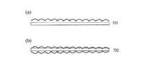
また、拡散材を添加する替わりに、図16(a)に示すように、片面に凹凸が設けられた光学板701または、図16(b)に示すように両面に凹凸が設けられた光学板702を用いてもよい。このように光を拡散する理由は照明装置114から出射する光の均斉度を高めるためである。したがって、照明ユニット509から出射する光の光量に差がなく均一に発光しているのであればこのような拡散手段は不要である。本実施形態においては、シリカが少量混入された2mm厚のアクリル板を光学板508として使用する。 Further, instead of adding a diffusing material, as shown in FIG. 16 (a), an
光学シート507は、数十μmから数百μmの厚さを有し、光学板508と同様、少量シリカなどの拡散材が混入されたアクリルなどの樹脂からなる。本実施形態においては、少量のシリカが添加された150μmの厚さの拡散シートを使用した。シリカにより、光学板508による光を若干拡散させることで均斉度の向上を調整している。 The
このように均斉度を高めるために光学板508および光学シート507を使用しているため、マトリクス状に配置された照明ユニット509から出射する光の均斉度が基準値以上であれば、光学板508および光学シート507の少なくとも一方を省略してもよい。逆に、マトリクス状に配置された照明ユニット509から出射する光の均斉度が高くない場合には、光学シート507を複数用いてもよい。 Since the
また、光学板508および光学シート507は、液晶パネル501の偏光板503から反射された光の偏光を変化させて反射する役割も果たす。シリカが混入されたり、上面、または両面に凹凸にあることによって偏光を変化させて反射する効果が向上する。 In addition, the
本実施形態の液晶表示装置では、照明装置114における光学板508と光学シート507との間に偏光を制御する光学部品を設置する必要がなく、簡単な光学板508および光学シート507のみを備えることによって部品点数が少なく、かつ正面輝度や輝度効率が高い照明装置504を実現できることが特長である。さらに、照明ユニット509から出射する光の偏光性が映像の画質に影響を及ぼさないほど高いときは偏光板503を使用しなくてもよい。これにより、さらに部品点数を少なくすることができ、製造コストを削減することができる。 In the liquid crystal display device of this embodiment, it is not necessary to install an optical component for controlling polarization between the
なお、均斉度を向上させるためには、照明装置の出射面における窒化物系半導体発光素子の発光領域の占める割合を高めることが重要である。このためには、照明ユニット509間の間隔をできるだけ短くする。例えば、図14に示す照明ユニット509において、パッケージ202の裏面に設けられた配線204がパッケージ202からはみ出ないように構成することによって、図17に示すように、筐体511内において、複数の照明ユニット509を隙間なくマトリクス状に配置し、均斉度を高めることができる。この場合、光学板508や光学シート507を用いなくても高い均斉度を有する照明装置が実現する。 In order to improve the uniformity, it is important to increase the ratio of the light emitting region of the nitride-based semiconductor light emitting element on the exit surface of the lighting device. For this purpose, the interval between the
図18は、5×8で照明ユニット509が配列された照明装置114において、照明ユニット509の各々を独立に制御できるように点灯回路を配置した照明装置114の駆動回路の一例を示している。 FIG. 18 shows an example of a drive circuit of the
このように個々の照明ユニット509の光量を制御することによって、液晶パネル113に表示される映像のコントラストを高めるとともにエネルギーを節減することができる。 In this way, by controlling the light quantity of each
上記実施形態では、照明ユニット509をマトリクス状に配置していた。しかし、照明ユニット509から出射する光の強度が高い場合には、照明ユニット509の数を減らしたバックライトとして機能する表示装置を実現してもよい。 In the above embodiment, the
図19(a)は、本実施形態の液晶表示装置に用いられる他の照明装置115の構造を模式的に示している。照明装置115は複数の照明部116を備えている。図19(b)は照明部116の構造を模式的に示している。照明部116は、導光板521と、一対の照明ユニット509とを備える。 FIG. 19A schematically shows the structure of another
導光板521は例えば液晶パネル501の横方向の長さと同程度の長さを有している。導光板521の両端には、照明ユニット509が配置され、照明ユニット509から出射する光が導光板521内を透過する。導光板521は1〜3mm程度の厚さを有し、アクリル系樹脂のメタクリルスチレン(MS)、ポリカボネート(PC)、ゼオノア等の樹脂でからなる。本実施形態では2mm厚のアクリル板を用いた。導光板521内には光路変換素子522が所定の間隔で複数配置されている。光路変換素子522は、導光板521内透過する光の一部を垂直に反射し、導光板521の表面から出射させる。光路変換素子522は、例えば、ホログラムやハーフミラーなどからなる。本実施形態ではホログラムを用いる。このような構成によって、照明ユニット509から出射する光の偏光を保ちながら導光板521の主面から偏光を出射することができる。 The
照明装置115は液晶パネル501の縦方向に複数の照明部116を備える。照明部116の数や、導光板521に設ける光路変換素子522の数は、照明ユニット509から出射する光の強度、照明装置115に求められる光の強度、出射する光の均斉度に応じて決定される。本実施形態では5つの照明部116が照明部116の長手方向に対して垂直な方向に配列されている。これにより、5つの照明部116の主面から同じ方向に偏光した光が出射する。均斉度の向上や液晶パネルから反射された光をもう一度反射するために光学板508や光学シート507を使用してもよい。 The
照明装置115を用いた場合でも、従来必要であったレンズシート406および輝度上昇フィルムを省略できるため、製造コストを低減し、光の利用効率が高く、低消費電力の液晶表示装置が実現する。 Even when the illuminating
なお、本実施形態の照明装置114に用いられる照明ユニット509や509'や発光ユニット510B、510G、510Rは、液晶表示装置以外の照明に用いてもよい。第1の実施形態で説明したように、青色、緑色および赤色を発光する窒化物系半導体発光素子に与える電力を調節することによって、一方向に偏光した任意の波長の可視光を出射することのできる照明装置として、種々の用途に使用することができる。 Note that the
また、上記第1から第3の実施形態の窒化物系半導体発光素子や照明装置において、波長変換のための蛍光物質を設けてもよい。これにより、波長帯域の拡大した光を出射することのできる光源を実現することができる。 Further, in the nitride-based semiconductor light-emitting elements and lighting devices of the first to third embodiments, a fluorescent material for wavelength conversion may be provided. Thereby, the light source which can radiate | emit the light which expanded the wavelength band is realizable.
(第4の実施形態)
以下、本発明の窒化物系半導体発光素子、照明装置および液晶表示装置のさらに他の実施形態を説明する。本実施形態の窒化物系半導体発光素子、照明装置および液晶表示装置は、窒化物系半導体発光素子が、m面から1°以上の角度で傾斜させた面を主面とする活性層領域を備えている点で、第1、第2の実施形態の窒化物系半導体発光素子および照明装置ならびに第3の実施形態の液晶表示装置と異なる。以下、第1の実施形態の窒化物系半導体発光素子を参照しながら本実施形態を説明するが、本実施形態の窒化物系半導体発光素子、照明装置および液晶表示装置も、以下で説明するような傾きの主面を有する活性層領域を備えている。(Fourth embodiment)
Hereinafter, other embodiments of the nitride-based semiconductor light-emitting element, the illumination device, and the liquid crystal display device of the present invention will be described. The nitride-based semiconductor light-emitting device, the illumination device, and the liquid crystal display device according to this embodiment include an active layer region in which a nitride-based semiconductor light-emitting device has a main surface that is inclined at an angle of 1 ° or more from the m-plane. In that respect, the nitride-based semiconductor light-emitting elements and illumination devices of the first and second embodiments are different from the liquid crystal display device of the third embodiment. Hereinafter, the present embodiment will be described with reference to the nitride-based semiconductor light-emitting device of the first embodiment, but the nitride-based semiconductor light-emitting device, the illumination device, and the liquid crystal display device of the present embodiment will also be described below. An active layer region having a principal surface with a large inclination is provided.
図3を参照しながら第1の実施形態で説明したように、活性層領域24を含む窒化物系半導体積層構造10はGaN基板10上にエピタキシャル成長される。m面から1°以上の角度で傾斜させた面を主面とする活性層領域10を成長させるため、本実施形態の窒化物系半導体発光素子では、図3に示すGaN基板10の主面がm面から1°以上の角度で傾斜していることが好ましい。このようなGaN基板10は、一般に「オフ基板」と称される。オフ基板は、単結晶インゴットから基板をスライスし、基板の表面を研磨する工程で、意図的にm面から特定方位に傾斜した面を主面とするように作製され得る。このように傾斜した基板の主面上に、各種半導体層が積層されると、これらの半導体層の表面(主面)もm面から傾斜する。 As described in the first embodiment with reference to FIG. 3, the nitride-based
したがって、本実施形態の窒化物系半導体発光素子においても、窒化物半導体積層構造20に含まれる活性層領域24、第1導電型の半導体層22および第2導電型の半導体層26もそれぞれm面から1°以上の角度で傾斜した主面を有している。なお、GaN基板10に替えて、例えば、m面から特定方向に傾斜した面を表面とするサファイア基板やSiC基板を用いてもよい。 Therefore, also in the nitride semiconductor light emitting device of this embodiment, the
次に、図20(a)および(b)を参照しながら、本実施形態における活性層領域の傾斜について詳細を説明する。 Next, the inclination of the active layer region in the present embodiment will be described in detail with reference to FIGS. 20 (a) and 20 (b).
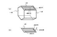
図20(a)は、GaN系化合物半導体の結晶構造(ウルツ鉱型結晶構造)を模式的に示す図であり、図2(a)の結晶構造の向きを90°回転させた構造を示している。GaN結晶のc面には、+c面および−c面が存在する。+c面はGa原子が表面に現れた(0001)面であり、「Ga面」と称される。一方、−c面はN(窒素)原子が表面に現れた(000−1)面であり、「N面」と称される。+c面と−c面とは平行な関係にあり、いずれも、m面に対して垂直である。c面は、極性を有するため、このように、c面を+c面と−c面に分けることができるが、非極性面であるa面を、+a面と−a面に区別する意義はない。 FIG. 20A is a diagram schematically showing a crystal structure (wurtzite crystal structure) of a GaN-based compound semiconductor, and shows a structure obtained by rotating the crystal structure direction of FIG. 2A by 90 °. Yes. There are a + c plane and a −c plane on the c-plane of the GaN crystal. The + c plane is a (0001) plane in which Ga atoms appear on the surface, and is referred to as a “Ga plane”. On the other hand, the -c plane is a (000-1) plane in which N (nitrogen) atoms appear on the surface, and is referred to as an "N plane". The + c plane and the −c plane are parallel to each other, and both are perpendicular to the m plane. Since the c-plane has polarity, the c-plane can be divided into a + c-plane and a −c-plane as described above, but there is no significance in distinguishing the non-polar a-plane into the + a-plane and the −a-plane. .
図20(a)に示す+c軸方向は、−c面から+c面に垂直に延びる方向である。一方、a軸方向は、図1の基本ベクトルa2に対応し、m面に平行な[−12−10]方向を向いている。図20(b)は、m面の法線、+c軸方向、およびa軸方向の相互関係を示す斜視図である。m面の法線は、[10−10]方向に平行であり、図20(b)に示されるように、+c軸方向およびa軸方向の両方に垂直である。The + c axis direction shown in FIG. 20A is a direction extending perpendicularly from the −c plane to the + c plane. On the other hand, the a-axis direction corresponds to the basic vector a2 in FIG. 1 and faces the [-12-10] direction parallel to the m-plane. FIG. 20B is a perspective view showing the correlation between the normal of the m-plane, the + c-axis direction, and the a-axis direction. The normal of the m-plane is parallel to the [10-10] direction and is perpendicular to both the + c-axis direction and the a-axis direction, as shown in FIG.
GaN系化合物半導体層の主面がm面から1°以上の角度で傾斜するということは、この半導体層の主面の法線がm面の法線から1°以上の角度で傾斜することを意味する。 The fact that the main surface of the GaN-based compound semiconductor layer is inclined at an angle of 1 ° or more from the m-plane means that the normal line of the main surface of the semiconductor layer is inclined at an angle of 1 ° or more from the normal line of the m-plane. means.
次に、図21(a)および(b)を参照する。図21(a)および(b)は、それぞれ、GaN系化合物半導体層の主面およびm面の関係を示す断面図である。この図は、m面およびc面の両方に垂直な断面図である。図21(a)および(b)には、+c軸方向を示す矢印が示されている。図21(a)および(b)に示したように、m面は+c軸方向に対して平行である。従って、m面の法線ベクトルは、+c軸方向に対して垂直である。 Next, refer to FIGS. 21A and 21B. FIGS. 21A and 21B are cross-sectional views showing the relationship between the main surface and the m-plane of the GaN-based compound semiconductor layer, respectively. This figure is a cross-sectional view perpendicular to both the m-plane and the c-plane. FIGS. 21A and 21B show an arrow indicating the + c axis direction. As shown in FIGS. 21A and 21B, the m-plane is parallel to the + c-axis direction. Accordingly, the normal vector of the m-plane is perpendicular to the + c axis direction.
図21(a)および(b)に示す例では、GaN系化合物半導体層における主面の法線ベクトルが、m面の法線ベクトルからc軸方向に傾斜している。より詳細に述べれば、図21(a)の例では、主面の法線ベクトルは+c面の側に傾斜しているが、図21(b)の例では、主面の法線ベクトルは−c面の側に傾斜している。本明細書では、前者の場合におけるm面の法線べクトルに対する主面の法線ベクトルの傾斜角度(傾斜角度θ)を正の値にとり、後者の場合における傾斜角度θを負の値にとることにする。いずれの場合でも、「主面はc軸方向に傾斜している」といえる。 In the example shown in FIGS. 21A and 21B, the normal vector of the main surface in the GaN-based compound semiconductor layer is inclined in the c-axis direction from the normal vector of the m-plane. More specifically, in the example of FIG. 21A, the normal vector of the main surface is inclined toward the + c plane, but in the example of FIG. 21B, the normal vector of the main surface is −. Inclined to the c-plane side. In the present specification, the inclination angle (inclination angle θ) of the normal vector of the principal surface with respect to the normal vector of the m plane in the former case is a positive value, and the inclination angle θ in the latter case is a negative value. I will decide. In either case, it can be said that “the main surface is inclined in the c-axis direction”.
本実施形態では、活性層領域24の主面の傾斜角度が1°以上5°以下の範囲にある場合、および、傾斜角度が−5°以上−1°以下の範囲にある場合、傾斜角度が0°より大きく±1°未満の場合と同様に本発明の効果を奏することができる。以下、図22(a)および(b)を参照しながら、この理由を説明する。図22(a)および(b)は、それぞれ、図21(a)および(b)に対応する断面図であり、m面からc軸方向に傾斜した活性層領域24における主面の近傍領域を示している。傾斜角度θの絶対値が5°以下の場合には、図22(a)および(b)に示すように、活性層領域24の主面に複数のステップが形成される。各ステップは、単原子層分の高さ(2.7Å)を有し、ほぼ等間隔(30Å以上)で平行に並んでいる。このようなステップの配列により、全体としてm面から傾斜した主面が形成されるが、微視的には多数のm面領域が露出していると考えられる。主面がm面から傾斜した活性層領域24がこのような構造となるのは、m面がもともと結晶面として非常に安定だからである。 In the present embodiment, when the inclination angle of the main surface of the
主面の法線ベクトルの傾斜方向が+c面および−c面以外の面方位を向いていても、主面がm面から傾斜した活性層領域24は同様の構造を備えていると考えられる。主面の法線ベクトルが例えばa軸方向に傾斜していても、傾斜角度が1°以上5°以下の範囲にあれば同様であると考えられる。 Even if the inclination direction of the normal vector of the main surface is directed to a plane orientation other than the + c plane and the −c plane, the
したがって、m面から任意の方位に1°以上5°以下の角度で傾斜した面を主面とする活性層領域24であっても、第1から第3の実施形態で詳細に説明したように、a軸と平行な方向に偏光しており、かつ、半導体チップの機械的強度を高めるには、半導体チップは厚い方が好ましい。また、発光波長が長くなるほど、偏光比が減少をし始める半導体チップの厚さは大きくなる。 Accordingly, as described in detail in the first to third embodiments, even in the
なお、傾斜角度θの絶対値が5°より大きくなると、ピエゾ電界によって内部量子効率が低下する。このため、ピエゾ電界が顕著に発生するのであれば、m面成長により半導体発光素子を実現することの意義が小さくなる。したがって、本発明では、傾斜角度θの絶対値を5°以下に制限する。しかし、傾斜角度θを例えば5°に設定した場合でも、製造ばらつきにより、現実の傾斜角度θは5°から±1°程度ずれる可能性がある。このような製造ばらつきを完全に排除することは困難であり、また、この程度の微小な角度ずれは、本発明の効果を妨げるものでもない。 If the absolute value of the tilt angle θ is greater than 5 °, the internal quantum efficiency is reduced by the piezoelectric field. For this reason, if a piezo electric field is remarkably generated, the significance of realizing a semiconductor light emitting device by m-plane growth is reduced. Therefore, in the present invention, the absolute value of the inclination angle θ is limited to 5 ° or less. However, even when the inclination angle θ is set to 5 °, for example, the actual inclination angle θ may be shifted from 5 ° by about ± 1 ° due to manufacturing variations. It is difficult to completely eliminate such manufacturing variations, and such a small angular deviation does not hinder the effects of the present invention.
本発明によれば、ダイシングや実装時のチップ破損率を低減しながら、照明装置として十分な偏光比を実現することが可能となる。したがって、従来、機械的強度の悪さから積極的な利用が困難であった、m面基板上で結晶成長させたGaN系半導体発光素子を種々の分野における光源として使用することができる。また、偏光特性を生かした、高効率で低コストな照明装置や液晶表示装置を実現できる。 ADVANTAGE OF THE INVENTION According to this invention, it becomes possible to implement | achieve sufficient polarization ratio as an illuminating device, reducing the chip | tip breakage rate at the time of dicing or mounting. Therefore, a GaN-based semiconductor light-emitting element that has been conventionally crystal-grown on an m-plane substrate, which has been difficult to actively use due to poor mechanical strength, can be used as a light source in various fields. In addition, it is possible to realize a highly efficient and low-cost illumination device or liquid crystal display device utilizing the polarization characteristics.
10 基板(GaN系基板)
12 表面(m面)
20 半導体積層構造
22 第1導電型の半導体層
24 活性層領域
26 第2導電型の半導体層
30 第1導電型電極
40 第2導電型電極
42 凹部
50 支持基板
61 電源
62 実装基板
63 偏光板
64 対物レンズ
65 カメラ
66 検出部
67 シリコンディテクター
71 AlGaInP系発光素子
72 偏光フィルタ
100、301、302、303 窒化物系半導体発光素子
111、112、114 照明装置
113 液晶表示装置
202 パッケージ
203 バンプ
204 配線
205 光学レンズ
206 封止部材
501 液晶パネル
502、503 偏光板
507 光学シート
508、701、702 光学板
511、512 筐体
521 導光板
522 光路変換素子10 Substrate (GaN-based substrate)
12 Surface (m-plane)
DESCRIPTION OF
Claims (26)
Translated fromJapanese前記第1および第2の窒化物系半導体発光素子のそれぞれは半導体チップを備え、
前記半導体チップは、AlxInyGazN(x+y+z=1、x≧0、y≧0、z≧0)半導体から形成された窒化物系半導体積層構造を含み、前記窒化物系半導体積層構造は、窒化物半導体層からなる活性層領域を含み、
前記AlxInyGazN(x+y+z=1、x≧0、y≧0、z≧0)半導体は、GaN系半導体であり、
前記活性層領域は、m面から1°以上の角度で傾斜しており、前記活性層領域における主面の法線とm面の法線とが形成する角度が1°以上5°以下であり、
前記第1および第2の窒化物系半導体発光素子は、それぞれ前記活性層領域から偏光を出射し、
前記第1および第2の窒化物系半導体発光素子が出射する偏光の波長をそれぞれλ1およびλ2とし、前記第1および第2の窒化物系半導体発光素子の半導体チップの厚さをそれぞれd1およびd2としたとき、
λ1<λ2かつd1<d2
の関係を満たしている照明装置。An illumination device comprising at least first and second nitride-based semiconductor light-emitting elements,
Each of the first and second nitride-based semiconductor light emitting devices includes a semiconductor chip,
The semiconductor chipis, Al x In y Ga z N (x + y + z = 1, x ≧ 0, y ≧ 0, z ≧ 0) includes a nitride-based semiconductor multilayer structure formed from a semiconductor, the nitride-based semiconductor multilayer structure Includes an active layer region made of a nitride semiconductor layer,
TheAl x In y Ga z N ( x + y + z = 1, x ≧ 0, y ≧ 0, z ≧ 0)semiconductor is a GaN-based semiconductor,
The active layer region is inclined at an angle of 1 ° or more from the m-plane, and an angle formed by the normal of the main surface and the normal of the m-plane in the active layer region is 1 ° or more and 5 ° or less. ,
The first and second nitride-based semiconductor light emitting devices each emit polarized light from the active layer region,
The wavelengths of polarized light emitted from the first and second nitride-based semiconductor light-emitting elements are λ1 and λ2, respectively, and the thicknesses of the semiconductor chips of the first and second nitride-based semiconductor light-emitting elements are d1 and d2, respectively. When
λ1 <λ2 and d1 <d2
Lighting equipment that satisfies the relationship of
前記第3の窒化物系半導体発光素子が出射する偏光の波長をλ3とし、前記第3の窒化物系半導体発光素子の半導体チップの厚さをd3としたとき、
λ1<λ2<λ3かつd1<d2<d3
の関係を満たしている請求項1に記載の照明装置。A third nitride semiconductor light emitting device comprising the semiconductor chip;
When the wavelength of polarized light emitted from the third nitride semiconductor light emitting device is λ3 and the thickness of the semiconductor chip of the third nitride semiconductor light emitting device is d3,
λ1 <λ2 <λ3 and d1 <d2 <d3
The lighting device according to claim 1, wherein:
前記第1、第2および第3の窒化物系半導体発光素子は前記支持基板上に支持されている、請求項3に記載の照明装置。It further has a support substrate,
The lighting device according to claim 3, wherein the first, second, and third nitride-based semiconductor light-emitting elements are supported on the support substrate.
前記AlGaInP系発光素子から出射する光が透過する位置に設けられた偏光フィルタと、
をさらに備え、前記λ1およびλ2は、それぞれ青色領域および緑色領域の波長である、請求項1に記載の照明装置。An AlGaInP-based light emitting element;
A polarizing filter provided at a position where light emitted from the AlGaInP-based light emitting element is transmitted;
The illuminating device according to claim 1, wherein λ1 and λ2 are wavelengths in a blue region and a green region, respectively.
光学シートと、
光学板と、
を備える照明装置。A plurality of lighting devices according to claim 12 or 13,
An optical sheet;
An optical plate;
A lighting device comprising:
前記半導体チップは、AlxInyGazN(x+y+z=1、x≧0、y≧0、z≧0)半導体から形成された窒化物系半導体積層構造を含み、
前記AlxInyGazN(x+y+z=1、x≧0、y≧0、z≧0)半導体は、GaN系半導体であり、
前記窒化物系半導体積層構造は、窒化物半導体層からなる活性層領域を有しており、
前記活性層領域は、m面から1°以上の角度で傾斜しており、前記活性層領域における主面の法線とm面の法線とが形成する角度が1°以上5°以下であり、
前記活性層領域から430nm以上470nm以下の波長の偏光を出射し、
前記半導体チップの厚さが110μm以上150μm以下であり、
前記半導体チップは、m面を表面とするGaN系半導体からなる基板を含む、窒化物系半導体発光素子。A nitride semiconductor light emitting device including a semiconductor chip,
The semiconductor chip includes a nitride-based semiconductor multilayer structure formed of Alx Iny Gaz N (x + y + z = 1, x ≧ 0, y ≧ 0, z ≧ 0) semiconductor,
TheAl x In y Ga z N ( x + y + z = 1, x ≧ 0, y ≧ 0, z ≧ 0)semiconductor is a GaN-based semiconductor,
The nitride-based semiconductor multilayer structure has an active layer region composed of a nitride semiconductor layer,
The active layer region is inclined at an angle of 1 ° or more from the m-plane, and an angle formed by the normal of the main surface and the normal of the m-plane in the active layer region is 1 ° or more and 5 ° or less. ,
The polarized light having a wavelength of430 nm or more and 470nm or less is emitted from the active layer region,
The thickness of the semiconductor chipRi der than 150μm or less 110 [mu]m,
The semiconductor chip is a nitride-based semiconductor light-emitting deviceincluding a substrate made of a GaN-based semiconductor having an m-plane as a surface .
前記半導体チップは、AlxInyGazN(x+y+z=1、x≧0、y≧0、z≧0)半導体から形成された窒化物系半導体積層構造を含み、
前記AlxInyGazN(x+y+z=1、x≧0、y≧0、z≧0)半導体は、GaN系半導体であり、
前記窒化物系半導体積層構造は、窒化物半導体層からなる活性層領域を有しており、
前記活性層領域は、m面から1°以上の角度で傾斜しており、前記活性層領域における主面の法線とm面の法線とが形成する角度が1°以上5°以下であり、
前記活性層領域から520nm以上560nm以下の波長の偏光を出射し、
前記半導体チップの厚さが200μm以上240μm以下であり、前記半導体チップは、m面を表面とするGaN系半導体からなる基板を含む、窒化物系半導体発光素子。A nitride semiconductor light emitting device including a semiconductor chip,
The semiconductor chip includes a nitride-based semiconductor multilayer structure formed of Alx Iny Gaz N (x + y + z = 1, x ≧ 0, y ≧ 0, z ≧ 0) semiconductor,
TheAl x In y Ga z N ( x + y + z = 1, x ≧ 0, y ≧ 0, z ≧ 0)semiconductor is a GaN-based semiconductor,
The nitride-based semiconductor multilayer structure has an active layer region composed of a nitride semiconductor layer,
The active layer region is inclined at an angle of 1 ° or more from the m-plane, and an angle formed by the normal of the main surface and the normal of the m-plane in the active layer region is 1 ° or more and 5 ° or less. ,
The polarized light having a wavelength of 520 nm or more and 560 nm or less is emitted from the active layer region,
The thickness of the semiconductor chipRi der than 240μm or less 200 [mu]m, wherein the semiconductor chip comprises a substrate made of GaN-based semiconductor to the surface of m-plane nitride-based semiconductor light-emitting device.
前記半導体チップは、AlxInyGazN(x+y+z=1、x≧0、y≧0、z≧0)半導体から形成された窒化物系半導体積層構造を含み、
前記AlxInyGazN(x+y+z=1、x≧0、y≧0、z≧0)半導体は、GaN系半導体であり、
前記窒化物系半導体積層構造は、窒化物半導体層からなる活性層領域を有しており、
前記活性層領域は、m面から1°以上の角度で傾斜しており、前記活性層領域における主面の法線とm面の法線とが形成する角度が1°以上5°以下であり、
前記活性層領域から590nmの波長の偏光を出射し、
前記半導体チップの厚さが250μm以上290μm以下であり、
前記半導体チップは、m面を表面とするGaN系半導体からなる基板を含む、窒化物系半導体発光素子。A nitride semiconductor light emitting device including a semiconductor chip,
The semiconductor chip includes a nitride-based semiconductor multilayer structure formed of Alx Iny Gaz N (x + y + z = 1, x ≧ 0, y ≧ 0, z ≧ 0) semiconductor,
TheAl x In y Ga z N ( x + y + z = 1, x ≧ 0, y ≧ 0, z ≧ 0)semiconductor is a GaN-based semiconductor,
The nitride-based semiconductor multilayer structure has an active layer region composed of a nitride semiconductor layer,
The active layer region is inclined at an angle of 1 ° or more from the m-plane, and an angle formed by the normal of the main surface and the normal of the m-plane in the active layer region is 1 ° or more and 5 ° or less. ,
The polarized light having a wavelength of590 nm is emitted from the active layer region,
The thickness of the semiconductor chipRi der than 290μm or less 250 [mu]m,
The semiconductor chip is a nitride-based semiconductor light-emitting deviceincluding a substrate made of a GaN-based semiconductor having an m-plane as a surface .
基板を用意する工程(a)と、
窒化物半導体層からなる活性層領域を有しており、AlxInyGazN(x+y+z=1、x≧0、y≧0、z≧0)半導体から形成された窒化物系半導体積層構造を前記基板上に形成する工程であって、前記活性層領域を、m面から1°以上の角度で傾斜させ、前記活性層領域における主面の法線とm面の法線とが形成する角度が1°以上5°以下である前記窒化物系半導体積層構造を前記基板上に形成する工程(b)と、
前記窒化物系半導体積層構造に電極を形成し、前記活性層領域から偏光を出射する半導体チップを作製する工程(c)と、
前記活性層領域から出射する偏光の波長に応じた厚さとなるように、前記半導体チップの厚さを調整する工程(d)と、
を含み、発光波長および半導体チップの厚さがそれぞれ互いに異なる第1および第2の窒化物系半導体発光素子を作製する工程(A)と、
前記第1および第2の窒化物系半導体発光素子を支持基板上に配置する工程(B)と、
を包含し、
前記AlxInyGazN(x+y+z=1、x≧0、y≧0、z≧0)半導体は、GaN系半導体であり、
前記工程(A)の前記工程(d)において、
前記第1および第2の窒化物系半導体発光素子が出射する偏光の波長をそれぞれλ1およびλ2とし、前記第1および第2の窒化物系半導体発光素子の半導体チップの厚さをそれぞれd1およびd2としたとき、
λ1<λ2かつd1<d2
の関係を満たすように、前記第1および第2の窒化物系半導体発光素子の前記半導体チップの厚さをそれぞれ調整する照明装置の製造方法。A method of manufacturing a lighting device including at least first and second nitride-based semiconductor light-emitting elements,
Preparing a substrate (a);
A nitride-based semiconductor multilayer structure having an active layer region made of a nitride semiconductor layer and formed from an Alx Iny Gaz N (x + y + z = 1, x ≧ 0, y ≧ 0, z ≧ 0) semiconductor Is formed on the substrate, and the active layer region is inclined at an angle of 1 ° or more from the m-plane to form a normal of the main surface and a normal of the m-plane in the active layer region. Forming the nitride-based semiconductor multilayer structure having an angle of 1 ° or more and 5 ° or less on the substrate (b);
(C) forming an electrode on the nitride-based semiconductor multilayer structure, and producing a semiconductor chip that emits polarized light from the active layer region;
A step (d) of adjusting the thickness of the semiconductor chip so as to have a thickness corresponding to the wavelength of polarized light emitted from the active layer region;
A first and second nitride-based semiconductor light-emitting device having a light emission wavelength and a semiconductor chip thickness different from each other (A),
A step (B) of disposing the first and second nitride-based semiconductor light-emitting elements on a support substrate;
Including
TheAl x In y Ga z N ( x + y + z = 1, x ≧ 0, y ≧ 0, z ≧ 0)semiconductor is a GaN-based semiconductor,
In the step (d) of the step (A),
The wavelengths of polarized light emitted from the first and second nitride-based semiconductor light-emitting elements are λ1 and λ2, respectively, and the thicknesses of the semiconductor chips of the first and second nitride-based semiconductor light-emitting elements are d1 and d2, respectively. When
λ1 <λ2 and d1 <d2
The manufacturing method of the illuminating device which each adjusts the thickness of the said semiconductor chip of the said 1st and 2nd nitride semiconductor light emitting element so that the relationship may be satisfy | filled.
請求項24に記載の照明装置と、 An illumination device according to claim 24;
を備えた液晶表示装置。A liquid crystal display device.
Priority Applications (1)
| Application Number | Priority Date | Filing Date | Title |
|---|---|---|---|
| JP2011545084AJP4988069B2 (en) | 2009-12-09 | 2010-12-07 | Nitride-based semiconductor light-emitting element, lighting device, liquid crystal display device, and manufacturing method of lighting device |
Applications Claiming Priority (4)
| Application Number | Priority Date | Filing Date | Title |
|---|---|---|---|
| JP2009279358 | 2009-12-09 | ||
| JP2009279358 | 2009-12-09 | ||
| JP2011545084AJP4988069B2 (en) | 2009-12-09 | 2010-12-07 | Nitride-based semiconductor light-emitting element, lighting device, liquid crystal display device, and manufacturing method of lighting device |
| PCT/JP2010/007117WO2011070770A1 (en) | 2009-12-09 | 2010-12-07 | Nitride-based semiconductor light-emitting element, lighting device, liquid crystal display device, and method for producing lighting device |
Publications (2)
| Publication Number | Publication Date |
|---|---|
| JP4988069B2true JP4988069B2 (en) | 2012-08-01 |
| JPWO2011070770A1 JPWO2011070770A1 (en) | 2013-04-22 |
Family
ID=44145332
Family Applications (1)
| Application Number | Title | Priority Date | Filing Date |
|---|---|---|---|
| JP2011545084AExpired - Fee RelatedJP4988069B2 (en) | 2009-12-09 | 2010-12-07 | Nitride-based semiconductor light-emitting element, lighting device, liquid crystal display device, and manufacturing method of lighting device |
Country Status (5)
| Country | Link |
|---|---|
| US (1) | US8729579B2 (en) |
| EP (1) | EP2472608B1 (en) |
| JP (1) | JP4988069B2 (en) |
| CN (1) | CN102648535A (en) |
| WO (1) | WO2011070770A1 (en) |
Families Citing this family (4)
| Publication number | Priority date | Publication date | Assignee | Title |
|---|---|---|---|---|
| JP4815013B2 (en)* | 2009-04-09 | 2011-11-16 | パナソニック株式会社 | Nitride-based semiconductor light-emitting element, lighting device, liquid crystal display device, and manufacturing method of lighting device |
| WO2013008380A1 (en)* | 2011-07-14 | 2013-01-17 | パナソニック株式会社 | Nitride semiconductor light-emitting element |
| KR102100936B1 (en)* | 2013-07-10 | 2020-04-16 | 서울바이오시스 주식회사 | Led chip having esd protection |
| US11307434B2 (en)* | 2016-09-01 | 2022-04-19 | 3D Live, Inc. | Stereoscopic display apparatus employing light emitting diodes with polarizing film/lens materials |
Citations (3)
| Publication number | Priority date | Publication date | Assignee | Title |
|---|---|---|---|---|
| JP2008198952A (en)* | 2007-02-15 | 2008-08-28 | Rohm Co Ltd | Group iii nitride semiconductor light emitting device |
| JP2008218645A (en)* | 2007-03-02 | 2008-09-18 | Rohm Co Ltd | Light emitting device |
| JP2009111012A (en)* | 2007-10-26 | 2009-05-21 | Rohm Co Ltd | Semiconductor light-emitting element |
Family Cites Families (28)
| Publication number | Priority date | Publication date | Assignee | Title |
|---|---|---|---|---|
| JP2859478B2 (en) | 1991-12-12 | 1999-02-17 | 日亜化学工業 株式会社 | Gallium nitride based compound semiconductor wafer cutting method for light emitting device |
| JP2748355B2 (en) | 1993-10-21 | 1998-05-06 | 日亜化学工業株式会社 | Method of manufacturing gallium nitride based compound semiconductor chip |
| CN1300859C (en) | 1997-01-31 | 2007-02-14 | 松下电器产业株式会社 | Light emitting element |
| JP3087743B2 (en) | 1998-11-12 | 2000-09-11 | 住友電気工業株式会社 | Intermediate color LED |
| TW406442B (en) | 1998-07-09 | 2000-09-21 | Sumitomo Electric Industries | White colored LED and intermediate colored LED |
| JP3122644B2 (en) | 1998-09-10 | 2001-01-09 | シャープ株式会社 | Method for manufacturing semiconductor light emitting device |
| JP2001168388A (en) | 1999-09-30 | 2001-06-22 | Sharp Corp | Gallium nitride-based compound semiconductor chip, manufacturing method thereof, and gallium nitride-based compound semiconductor wafer |
| JP2001308462A (en) | 2000-04-21 | 2001-11-02 | Matsushita Electric Ind Co Ltd | Method for manufacturing nitride semiconductor device |
| US6999071B2 (en)* | 2000-05-19 | 2006-02-14 | Tibor Balogh | Method and apparatus for displaying 3d images |
| WO2003025263A1 (en)* | 2001-09-13 | 2003-03-27 | Japan Science And Technology Agency | Nitride semiconductor substrate, its manufacturing method, and semiconductor optical device using the same |
| JP2003332697A (en) | 2002-05-09 | 2003-11-21 | Sony Corp | Nitride semiconductor element and its manufacturing method |
| US7186004B2 (en)* | 2002-12-31 | 2007-03-06 | Karlton David Powell | Homogenizing optical sheet, method of manufacture, and illumination system |
| WO2007002151A2 (en) | 2005-06-21 | 2007-01-04 | The Regents Of The University Of California | Packaging technique for the fabrication of polarized light emitting diodes |
| JP4661735B2 (en) | 2005-09-21 | 2011-03-30 | 日本ビクター株式会社 | Surface light source device |
| TWI306316B (en)* | 2006-07-28 | 2009-02-11 | Huga Optotech Inc | Semiconductor light emitting device and method of fabricating the same |
| JP2008159606A (en) | 2006-12-20 | 2008-07-10 | Rohm Co Ltd | Nitride semiconductor light emitting device and manufacturing method thereof |
| JP4062360B2 (en) | 2007-03-08 | 2008-03-19 | 松下電器産業株式会社 | Light emitting element |
| US20080225202A1 (en)* | 2007-03-15 | 2008-09-18 | Hanbitt Joo | Optical sheet and liquid crystal display device having the same |
| JP2008235804A (en) | 2007-03-23 | 2008-10-02 | Rohm Co Ltd | Light emitting element |
| JP2008258503A (en) | 2007-04-06 | 2008-10-23 | Sumitomo Electric Ind Ltd | Nitride-based semiconductor light-emitting device and method for manufacturing nitride-based semiconductor light-emitting device |
| JP2008305962A (en) | 2007-06-07 | 2008-12-18 | Rohm Co Ltd | Optical device |
| JP2009021349A (en) | 2007-07-11 | 2009-01-29 | Rohm Co Ltd | Manufacturing method of semiconductor light-emitting element, and semiconductor light-emitting element |
| JP2009044067A (en) | 2007-08-10 | 2009-02-26 | Rohm Co Ltd | Semiconductor light emitting element |
| US7858995B2 (en) | 2007-08-03 | 2010-12-28 | Rohm Co., Ltd. | Semiconductor light emitting device |
| JP5309386B2 (en) | 2007-08-20 | 2013-10-09 | 国立大学法人北海道大学 | Semiconductor light emitting element array, manufacturing method thereof, and optical transmitter |
| JP4631884B2 (en)* | 2007-08-22 | 2011-02-16 | 日立電線株式会社 | Sphalerite-type nitride semiconductor free-standing substrate, method for manufacturing zinc-blende nitride semiconductor free-standing substrate, and light-emitting device using zinc-blende nitride semiconductor free-standing substrate |
| JP2009070893A (en) | 2007-09-11 | 2009-04-02 | Rohm Co Ltd | Light-emitting device and manufacturing method therefor |
| KR100882112B1 (en)* | 2007-09-28 | 2009-02-06 | 삼성전기주식회사 | Semiconductor light emitting device and manufacturing method thereof |
- 2010
- 2010-12-07JPJP2011545084Apatent/JP4988069B2/ennot_activeExpired - Fee Related
- 2010-12-07CNCN2010800428832Apatent/CN102648535A/enactivePending
- 2010-12-07EPEP10835696.5Apatent/EP2472608B1/ennot_activeNot-in-force
- 2010-12-07WOPCT/JP2010/007117patent/WO2011070770A1/enactiveApplication Filing
- 2012
- 2012-03-28USUS13/432,022patent/US8729579B2/ennot_activeExpired - Fee Related
Patent Citations (3)
| Publication number | Priority date | Publication date | Assignee | Title |
|---|---|---|---|---|
| JP2008198952A (en)* | 2007-02-15 | 2008-08-28 | Rohm Co Ltd | Group iii nitride semiconductor light emitting device |
| JP2008218645A (en)* | 2007-03-02 | 2008-09-18 | Rohm Co Ltd | Light emitting device |
| JP2009111012A (en)* | 2007-10-26 | 2009-05-21 | Rohm Co Ltd | Semiconductor light-emitting element |
Also Published As
| Publication number | Publication date |
|---|---|
| WO2011070770A1 (en) | 2011-06-16 |
| US8729579B2 (en) | 2014-05-20 |
| EP2472608B1 (en) | 2013-09-18 |
| EP2472608A1 (en) | 2012-07-04 |
| US20120182495A1 (en) | 2012-07-19 |
| CN102648535A (en) | 2012-08-22 |
| JPWO2011070770A1 (en) | 2013-04-22 |
| EP2472608A4 (en) | 2012-09-26 |
Similar Documents
| Publication | Publication Date | Title |
|---|---|---|
| JP4815013B2 (en) | Nitride-based semiconductor light-emitting element, lighting device, liquid crystal display device, and manufacturing method of lighting device | |
| US7786493B2 (en) | Light emitting diode, method for manufacturing light emitting diode, integrated light emitting diode, method for manufacturing integrated light emitting diode, light emitting diode backlight, light emitting diode illumination device, light emitting diode display, electronic apparatus, electronic device, and method for manufacturing electronic device | |
| EP2605298A1 (en) | Semiconductor light-emitting device | |
| CN103996782B (en) | Light emitting device packaging piece and manufacture method thereof | |
| US20080179607A1 (en) | Non-polar and semi-polar light emitting devices | |
| US9117961B2 (en) | Nitride-based semiconductor light-emitting element | |
| CN102804415A (en) | Gallium nitride-based compound semiconductor light-emitting diode | |
| US8835967B2 (en) | Nitride-based semiconductor light-emitting device | |
| US20130105761A1 (en) | Light emitting device and method for manufacturing the same | |
| KR20160141035A (en) | Fabrication method of semiconductor light emitting device | |
| KR101552104B1 (en) | Semiconductor light emitting element | |
| KR102098591B1 (en) | Semiconductor light emitting device | |
| JP4988069B2 (en) | Nitride-based semiconductor light-emitting element, lighting device, liquid crystal display device, and manufacturing method of lighting device | |
| US8405093B2 (en) | Light emitting device | |
| KR20140061827A (en) | Semiconductor light emitting device and manufacturing method of semiconductor light emitting device | |
| JP5296264B1 (en) | Nitride semiconductor light emitting device and LED system | |
| KR20130062770A (en) | Light emitting device | |
| US10153397B2 (en) | Semiconductor light-emitting device | |
| US8435880B2 (en) | Method for manufacturing semiconductor device and semiconductor device | |
| US20250204093A1 (en) | Light emitting device and module having the same | |
| KR20130040009A (en) | Light emitting device package | |
| KR20120133834A (en) | Light emitting device and Manufacturing method for light emitting device | |
| DeMille | White light-emitting diodes based on nonpolar and semipolar gallium nitride orientations | |
| KR20130056368A (en) | Light emitting device |
Legal Events
| Date | Code | Title | Description |
|---|---|---|---|
| TRDD | Decision of grant or rejection written | ||
| A01 | Written decision to grant a patent or to grant a registration (utility model) | Free format text:JAPANESE INTERMEDIATE CODE: A01 Effective date:20120403 | |
| A01 | Written decision to grant a patent or to grant a registration (utility model) | Free format text:JAPANESE INTERMEDIATE CODE: A01 | |
| A61 | First payment of annual fees (during grant procedure) | Free format text:JAPANESE INTERMEDIATE CODE: A61 Effective date:20120425 | |
| R150 | Certificate of patent or registration of utility model | Ref document number:4988069 Country of ref document:JP Free format text:JAPANESE INTERMEDIATE CODE: R150 Free format text:JAPANESE INTERMEDIATE CODE: R150 | |
| FPAY | Renewal fee payment (event date is renewal date of database) | Free format text:PAYMENT UNTIL: 20150511 Year of fee payment:3 | |
| LAPS | Cancellation because of no payment of annual fees |