JP4987823B2 - Semiconductor device - Google Patents
Semiconductor deviceDownload PDFInfo
- Publication number
- JP4987823B2 JP4987823B2JP2008221534AJP2008221534AJP4987823B2JP 4987823 B2JP4987823 B2JP 4987823B2JP 2008221534 AJP2008221534 AJP 2008221534AJP 2008221534 AJP2008221534 AJP 2008221534AJP 4987823 B2JP4987823 B2JP 4987823B2
- Authority
- JP
- Japan
- Prior art keywords
- film
- semiconductor substrate
- bump
- solder bump
- grain boundary
- Prior art date
- Legal status (The legal status is an assumption and is not a legal conclusion. Google has not performed a legal analysis and makes no representation as to the accuracy of the status listed.)
- Expired - Fee Related
Links
Images


Classifications
- H—ELECTRICITY
- H01—ELECTRIC ELEMENTS
- H01L—SEMICONDUCTOR DEVICES NOT COVERED BY CLASS H10
- H01L24/00—Arrangements for connecting or disconnecting semiconductor or solid-state bodies; Methods or apparatus related thereto
- H01L24/01—Means for bonding being attached to, or being formed on, the surface to be connected, e.g. chip-to-package, die-attach, "first-level" interconnects; Manufacturing methods related thereto
- H01L24/10—Bump connectors ; Manufacturing methods related thereto
- H01L24/11—Manufacturing methods
- H—ELECTRICITY
- H01—ELECTRIC ELEMENTS
- H01L—SEMICONDUCTOR DEVICES NOT COVERED BY CLASS H10
- H01L24/00—Arrangements for connecting or disconnecting semiconductor or solid-state bodies; Methods or apparatus related thereto
- H01L24/01—Means for bonding being attached to, or being formed on, the surface to be connected, e.g. chip-to-package, die-attach, "first-level" interconnects; Manufacturing methods related thereto
- H01L24/10—Bump connectors ; Manufacturing methods related thereto
- H01L24/15—Structure, shape, material or disposition of the bump connectors after the connecting process
- H01L24/16—Structure, shape, material or disposition of the bump connectors after the connecting process of an individual bump connector
- H—ELECTRICITY
- H01—ELECTRIC ELEMENTS
- H01L—SEMICONDUCTOR DEVICES NOT COVERED BY CLASS H10
- H01L2224/00—Indexing scheme for arrangements for connecting or disconnecting semiconductor or solid-state bodies and methods related thereto as covered by H01L24/00
- H01L2224/01—Means for bonding being attached to, or being formed on, the surface to be connected, e.g. chip-to-package, die-attach, "first-level" interconnects; Manufacturing methods related thereto
- H01L2224/02—Bonding areas; Manufacturing methods related thereto
- H01L2224/03—Manufacturing methods
- H01L2224/034—Manufacturing methods by blanket deposition of the material of the bonding area
- H01L2224/03444—Manufacturing methods by blanket deposition of the material of the bonding area in gaseous form
- H01L2224/0345—Physical vapour deposition [PVD], e.g. evaporation, or sputtering
- H—ELECTRICITY
- H01—ELECTRIC ELEMENTS
- H01L—SEMICONDUCTOR DEVICES NOT COVERED BY CLASS H10
- H01L2224/00—Indexing scheme for arrangements for connecting or disconnecting semiconductor or solid-state bodies and methods related thereto as covered by H01L24/00
- H01L2224/01—Means for bonding being attached to, or being formed on, the surface to be connected, e.g. chip-to-package, die-attach, "first-level" interconnects; Manufacturing methods related thereto
- H01L2224/02—Bonding areas; Manufacturing methods related thereto
- H01L2224/03—Manufacturing methods
- H01L2224/034—Manufacturing methods by blanket deposition of the material of the bonding area
- H01L2224/0346—Plating
- H—ELECTRICITY
- H01—ELECTRIC ELEMENTS
- H01L—SEMICONDUCTOR DEVICES NOT COVERED BY CLASS H10
- H01L2224/00—Indexing scheme for arrangements for connecting or disconnecting semiconductor or solid-state bodies and methods related thereto as covered by H01L24/00
- H01L2224/01—Means for bonding being attached to, or being formed on, the surface to be connected, e.g. chip-to-package, die-attach, "first-level" interconnects; Manufacturing methods related thereto
- H01L2224/02—Bonding areas; Manufacturing methods related thereto
- H01L2224/03—Manufacturing methods
- H01L2224/039—Methods of manufacturing bonding areas involving a specific sequence of method steps
- H01L2224/03912—Methods of manufacturing bonding areas involving a specific sequence of method steps the bump being used as a mask for patterning the bonding area
- H—ELECTRICITY
- H01—ELECTRIC ELEMENTS
- H01L—SEMICONDUCTOR DEVICES NOT COVERED BY CLASS H10
- H01L2224/00—Indexing scheme for arrangements for connecting or disconnecting semiconductor or solid-state bodies and methods related thereto as covered by H01L24/00
- H01L2224/01—Means for bonding being attached to, or being formed on, the surface to be connected, e.g. chip-to-package, die-attach, "first-level" interconnects; Manufacturing methods related thereto
- H01L2224/02—Bonding areas; Manufacturing methods related thereto
- H01L2224/04—Structure, shape, material or disposition of the bonding areas prior to the connecting process
- H01L2224/0401—Bonding areas specifically adapted for bump connectors, e.g. under bump metallisation [UBM]
- H—ELECTRICITY
- H01—ELECTRIC ELEMENTS
- H01L—SEMICONDUCTOR DEVICES NOT COVERED BY CLASS H10
- H01L2224/00—Indexing scheme for arrangements for connecting or disconnecting semiconductor or solid-state bodies and methods related thereto as covered by H01L24/00
- H01L2224/01—Means for bonding being attached to, or being formed on, the surface to be connected, e.g. chip-to-package, die-attach, "first-level" interconnects; Manufacturing methods related thereto
- H01L2224/02—Bonding areas; Manufacturing methods related thereto
- H01L2224/04—Structure, shape, material or disposition of the bonding areas prior to the connecting process
- H01L2224/05—Structure, shape, material or disposition of the bonding areas prior to the connecting process of an individual bonding area
- H01L2224/05001—Internal layers
- H01L2224/0502—Disposition
- H01L2224/05023—Disposition the whole internal layer protruding from the surface
- H—ELECTRICITY
- H01—ELECTRIC ELEMENTS
- H01L—SEMICONDUCTOR DEVICES NOT COVERED BY CLASS H10
- H01L2224/00—Indexing scheme for arrangements for connecting or disconnecting semiconductor or solid-state bodies and methods related thereto as covered by H01L24/00
- H01L2224/01—Means for bonding being attached to, or being formed on, the surface to be connected, e.g. chip-to-package, die-attach, "first-level" interconnects; Manufacturing methods related thereto
- H01L2224/02—Bonding areas; Manufacturing methods related thereto
- H01L2224/04—Structure, shape, material or disposition of the bonding areas prior to the connecting process
- H01L2224/05—Structure, shape, material or disposition of the bonding areas prior to the connecting process of an individual bonding area
- H01L2224/05001—Internal layers
- H01L2224/05099—Material
- H01L2224/051—Material with a principal constituent of the material being a metal or a metalloid, e.g. boron [B], silicon [Si], germanium [Ge], arsenic [As], antimony [Sb], tellurium [Te] and polonium [Po], and alloys thereof
- H01L2224/05163—Material with a principal constituent of the material being a metal or a metalloid, e.g. boron [B], silicon [Si], germanium [Ge], arsenic [As], antimony [Sb], tellurium [Te] and polonium [Po], and alloys thereof the principal constituent melting at a temperature of greater than 1550°C
- H01L2224/05166—Titanium [Ti] as principal constituent
- H—ELECTRICITY
- H01—ELECTRIC ELEMENTS
- H01L—SEMICONDUCTOR DEVICES NOT COVERED BY CLASS H10
- H01L2224/00—Indexing scheme for arrangements for connecting or disconnecting semiconductor or solid-state bodies and methods related thereto as covered by H01L24/00
- H01L2224/01—Means for bonding being attached to, or being formed on, the surface to be connected, e.g. chip-to-package, die-attach, "first-level" interconnects; Manufacturing methods related thereto
- H01L2224/02—Bonding areas; Manufacturing methods related thereto
- H01L2224/04—Structure, shape, material or disposition of the bonding areas prior to the connecting process
- H01L2224/05—Structure, shape, material or disposition of the bonding areas prior to the connecting process of an individual bonding area
- H01L2224/0554—External layer
- H01L2224/0556—Disposition
- H01L2224/05563—Only on parts of the surface of the internal layer
- H01L2224/05564—Only on the bonding interface of the bonding area
- H—ELECTRICITY
- H01—ELECTRIC ELEMENTS
- H01L—SEMICONDUCTOR DEVICES NOT COVERED BY CLASS H10
- H01L2224/00—Indexing scheme for arrangements for connecting or disconnecting semiconductor or solid-state bodies and methods related thereto as covered by H01L24/00
- H01L2224/01—Means for bonding being attached to, or being formed on, the surface to be connected, e.g. chip-to-package, die-attach, "first-level" interconnects; Manufacturing methods related thereto
- H01L2224/02—Bonding areas; Manufacturing methods related thereto
- H01L2224/04—Structure, shape, material or disposition of the bonding areas prior to the connecting process
- H01L2224/05—Structure, shape, material or disposition of the bonding areas prior to the connecting process of an individual bonding area
- H01L2224/0554—External layer
- H01L2224/0556—Disposition
- H01L2224/05568—Disposition the whole external layer protruding from the surface
- H—ELECTRICITY
- H01—ELECTRIC ELEMENTS
- H01L—SEMICONDUCTOR DEVICES NOT COVERED BY CLASS H10
- H01L2224/00—Indexing scheme for arrangements for connecting or disconnecting semiconductor or solid-state bodies and methods related thereto as covered by H01L24/00
- H01L2224/01—Means for bonding being attached to, or being formed on, the surface to be connected, e.g. chip-to-package, die-attach, "first-level" interconnects; Manufacturing methods related thereto
- H01L2224/02—Bonding areas; Manufacturing methods related thereto
- H01L2224/04—Structure, shape, material or disposition of the bonding areas prior to the connecting process
- H01L2224/05—Structure, shape, material or disposition of the bonding areas prior to the connecting process of an individual bonding area
- H01L2224/0554—External layer
- H01L2224/05573—Single external layer
- H—ELECTRICITY
- H01—ELECTRIC ELEMENTS
- H01L—SEMICONDUCTOR DEVICES NOT COVERED BY CLASS H10
- H01L2224/00—Indexing scheme for arrangements for connecting or disconnecting semiconductor or solid-state bodies and methods related thereto as covered by H01L24/00
- H01L2224/01—Means for bonding being attached to, or being formed on, the surface to be connected, e.g. chip-to-package, die-attach, "first-level" interconnects; Manufacturing methods related thereto
- H01L2224/02—Bonding areas; Manufacturing methods related thereto
- H01L2224/04—Structure, shape, material or disposition of the bonding areas prior to the connecting process
- H01L2224/05—Structure, shape, material or disposition of the bonding areas prior to the connecting process of an individual bonding area
- H01L2224/0554—External layer
- H01L2224/05599—Material
- H01L2224/056—Material with a principal constituent of the material being a metal or a metalloid, e.g. boron [B], silicon [Si], germanium [Ge], arsenic [As], antimony [Sb], tellurium [Te] and polonium [Po], and alloys thereof
- H01L2224/05638—Material with a principal constituent of the material being a metal or a metalloid, e.g. boron [B], silicon [Si], germanium [Ge], arsenic [As], antimony [Sb], tellurium [Te] and polonium [Po], and alloys thereof the principal constituent melting at a temperature of greater than or equal to 950°C and less than 1550°C
- H01L2224/05647—Copper [Cu] as principal constituent
- H—ELECTRICITY
- H01—ELECTRIC ELEMENTS
- H01L—SEMICONDUCTOR DEVICES NOT COVERED BY CLASS H10
- H01L2224/00—Indexing scheme for arrangements for connecting or disconnecting semiconductor or solid-state bodies and methods related thereto as covered by H01L24/00
- H01L2224/01—Means for bonding being attached to, or being formed on, the surface to be connected, e.g. chip-to-package, die-attach, "first-level" interconnects; Manufacturing methods related thereto
- H01L2224/02—Bonding areas; Manufacturing methods related thereto
- H01L2224/04—Structure, shape, material or disposition of the bonding areas prior to the connecting process
- H01L2224/05—Structure, shape, material or disposition of the bonding areas prior to the connecting process of an individual bonding area
- H01L2224/0554—External layer
- H01L2224/05599—Material
- H01L2224/056—Material with a principal constituent of the material being a metal or a metalloid, e.g. boron [B], silicon [Si], germanium [Ge], arsenic [As], antimony [Sb], tellurium [Te] and polonium [Po], and alloys thereof
- H01L2224/05638—Material with a principal constituent of the material being a metal or a metalloid, e.g. boron [B], silicon [Si], germanium [Ge], arsenic [As], antimony [Sb], tellurium [Te] and polonium [Po], and alloys thereof the principal constituent melting at a temperature of greater than or equal to 950°C and less than 1550°C
- H01L2224/05655—Nickel [Ni] as principal constituent
- H—ELECTRICITY
- H01—ELECTRIC ELEMENTS
- H01L—SEMICONDUCTOR DEVICES NOT COVERED BY CLASS H10
- H01L2224/00—Indexing scheme for arrangements for connecting or disconnecting semiconductor or solid-state bodies and methods related thereto as covered by H01L24/00
- H01L2224/01—Means for bonding being attached to, or being formed on, the surface to be connected, e.g. chip-to-package, die-attach, "first-level" interconnects; Manufacturing methods related thereto
- H01L2224/10—Bump connectors; Manufacturing methods related thereto
- H01L2224/11—Manufacturing methods
- H01L2224/114—Manufacturing methods by blanket deposition of the material of the bump connector
- H01L2224/1146—Plating
- H—ELECTRICITY
- H01—ELECTRIC ELEMENTS
- H01L—SEMICONDUCTOR DEVICES NOT COVERED BY CLASS H10
- H01L2224/00—Indexing scheme for arrangements for connecting or disconnecting semiconductor or solid-state bodies and methods related thereto as covered by H01L24/00
- H01L2224/01—Means for bonding being attached to, or being formed on, the surface to be connected, e.g. chip-to-package, die-attach, "first-level" interconnects; Manufacturing methods related thereto
- H01L2224/10—Bump connectors; Manufacturing methods related thereto
- H01L2224/11—Manufacturing methods
- H01L2224/1147—Manufacturing methods using a lift-off mask
- H—ELECTRICITY
- H01—ELECTRIC ELEMENTS
- H01L—SEMICONDUCTOR DEVICES NOT COVERED BY CLASS H10
- H01L2224/00—Indexing scheme for arrangements for connecting or disconnecting semiconductor or solid-state bodies and methods related thereto as covered by H01L24/00
- H01L2224/01—Means for bonding being attached to, or being formed on, the surface to be connected, e.g. chip-to-package, die-attach, "first-level" interconnects; Manufacturing methods related thereto
- H01L2224/10—Bump connectors; Manufacturing methods related thereto
- H01L2224/11—Manufacturing methods
- H01L2224/118—Post-treatment of the bump connector
- H01L2224/11848—Thermal treatments, e.g. annealing, controlled cooling
- H01L2224/11849—Reflowing
- H—ELECTRICITY
- H01—ELECTRIC ELEMENTS
- H01L—SEMICONDUCTOR DEVICES NOT COVERED BY CLASS H10
- H01L2224/00—Indexing scheme for arrangements for connecting or disconnecting semiconductor or solid-state bodies and methods related thereto as covered by H01L24/00
- H01L2224/01—Means for bonding being attached to, or being formed on, the surface to be connected, e.g. chip-to-package, die-attach, "first-level" interconnects; Manufacturing methods related thereto
- H01L2224/10—Bump connectors; Manufacturing methods related thereto
- H01L2224/11—Manufacturing methods
- H01L2224/119—Methods of manufacturing bump connectors involving a specific sequence of method steps
- H—ELECTRICITY
- H01—ELECTRIC ELEMENTS
- H01L—SEMICONDUCTOR DEVICES NOT COVERED BY CLASS H10
- H01L2224/00—Indexing scheme for arrangements for connecting or disconnecting semiconductor or solid-state bodies and methods related thereto as covered by H01L24/00
- H01L2224/01—Means for bonding being attached to, or being formed on, the surface to be connected, e.g. chip-to-package, die-attach, "first-level" interconnects; Manufacturing methods related thereto
- H01L2224/10—Bump connectors; Manufacturing methods related thereto
- H01L2224/12—Structure, shape, material or disposition of the bump connectors prior to the connecting process
- H01L2224/13—Structure, shape, material or disposition of the bump connectors prior to the connecting process of an individual bump connector
- H01L2224/13001—Core members of the bump connector
- H01L2224/1302—Disposition
- H01L2224/13023—Disposition the whole bump connector protruding from the surface
- H—ELECTRICITY
- H01—ELECTRIC ELEMENTS
- H01L—SEMICONDUCTOR DEVICES NOT COVERED BY CLASS H10
- H01L2224/00—Indexing scheme for arrangements for connecting or disconnecting semiconductor or solid-state bodies and methods related thereto as covered by H01L24/00
- H01L2224/01—Means for bonding being attached to, or being formed on, the surface to be connected, e.g. chip-to-package, die-attach, "first-level" interconnects; Manufacturing methods related thereto
- H01L2224/10—Bump connectors; Manufacturing methods related thereto
- H01L2224/12—Structure, shape, material or disposition of the bump connectors prior to the connecting process
- H01L2224/13—Structure, shape, material or disposition of the bump connectors prior to the connecting process of an individual bump connector
- H01L2224/13001—Core members of the bump connector
- H01L2224/13099—Material
- H01L2224/131—Material with a principal constituent of the material being a metal or a metalloid, e.g. boron [B], silicon [Si], germanium [Ge], arsenic [As], antimony [Sb], tellurium [Te] and polonium [Po], and alloys thereof
- H01L2224/13101—Material with a principal constituent of the material being a metal or a metalloid, e.g. boron [B], silicon [Si], germanium [Ge], arsenic [As], antimony [Sb], tellurium [Te] and polonium [Po], and alloys thereof the principal constituent melting at a temperature of less than 400°C
- H01L2224/13111—Tin [Sn] as principal constituent
- H—ELECTRICITY
- H01—ELECTRIC ELEMENTS
- H01L—SEMICONDUCTOR DEVICES NOT COVERED BY CLASS H10
- H01L2224/00—Indexing scheme for arrangements for connecting or disconnecting semiconductor or solid-state bodies and methods related thereto as covered by H01L24/00
- H01L2224/01—Means for bonding being attached to, or being formed on, the surface to be connected, e.g. chip-to-package, die-attach, "first-level" interconnects; Manufacturing methods related thereto
- H01L2224/10—Bump connectors; Manufacturing methods related thereto
- H01L2224/15—Structure, shape, material or disposition of the bump connectors after the connecting process
- H01L2224/16—Structure, shape, material or disposition of the bump connectors after the connecting process of an individual bump connector
- H01L2224/161—Disposition
- H01L2224/16151—Disposition the bump connector connecting between a semiconductor or solid-state body and an item not being a semiconductor or solid-state body, e.g. chip-to-substrate, chip-to-passive
- H01L2224/16221—Disposition the bump connector connecting between a semiconductor or solid-state body and an item not being a semiconductor or solid-state body, e.g. chip-to-substrate, chip-to-passive the body and the item being stacked
- H01L2224/16225—Disposition the bump connector connecting between a semiconductor or solid-state body and an item not being a semiconductor or solid-state body, e.g. chip-to-substrate, chip-to-passive the body and the item being stacked the item being non-metallic, e.g. insulating substrate with or without metallisation
- H01L2224/16227—Disposition the bump connector connecting between a semiconductor or solid-state body and an item not being a semiconductor or solid-state body, e.g. chip-to-substrate, chip-to-passive the body and the item being stacked the item being non-metallic, e.g. insulating substrate with or without metallisation the bump connector connecting to a bond pad of the item
- H—ELECTRICITY
- H01—ELECTRIC ELEMENTS
- H01L—SEMICONDUCTOR DEVICES NOT COVERED BY CLASS H10
- H01L2224/00—Indexing scheme for arrangements for connecting or disconnecting semiconductor or solid-state bodies and methods related thereto as covered by H01L24/00
- H01L2224/01—Means for bonding being attached to, or being formed on, the surface to be connected, e.g. chip-to-package, die-attach, "first-level" interconnects; Manufacturing methods related thereto
- H01L2224/10—Bump connectors; Manufacturing methods related thereto
- H01L2224/15—Structure, shape, material or disposition of the bump connectors after the connecting process
- H01L2224/16—Structure, shape, material or disposition of the bump connectors after the connecting process of an individual bump connector
- H01L2224/165—Material
- H01L2224/16501—Material at the bonding interface
- H01L2224/16503—Material at the bonding interface comprising an intermetallic compound
- H—ELECTRICITY
- H01—ELECTRIC ELEMENTS
- H01L—SEMICONDUCTOR DEVICES NOT COVERED BY CLASS H10
- H01L2224/00—Indexing scheme for arrangements for connecting or disconnecting semiconductor or solid-state bodies and methods related thereto as covered by H01L24/00
- H01L2224/01—Means for bonding being attached to, or being formed on, the surface to be connected, e.g. chip-to-package, die-attach, "first-level" interconnects; Manufacturing methods related thereto
- H01L2224/10—Bump connectors; Manufacturing methods related thereto
- H01L2224/15—Structure, shape, material or disposition of the bump connectors after the connecting process
- H01L2224/16—Structure, shape, material or disposition of the bump connectors after the connecting process of an individual bump connector
- H01L2224/165—Material
- H01L2224/16505—Material outside the bonding interface, e.g. in the bulk of the bump connector
- H01L2224/16507—Material outside the bonding interface, e.g. in the bulk of the bump connector comprising an intermetallic compound
- H—ELECTRICITY
- H01—ELECTRIC ELEMENTS
- H01L—SEMICONDUCTOR DEVICES NOT COVERED BY CLASS H10
- H01L2224/00—Indexing scheme for arrangements for connecting or disconnecting semiconductor or solid-state bodies and methods related thereto as covered by H01L24/00
- H01L2224/80—Methods for connecting semiconductor or other solid state bodies using means for bonding being attached to, or being formed on, the surface to be connected
- H01L2224/81—Methods for connecting semiconductor or other solid state bodies using means for bonding being attached to, or being formed on, the surface to be connected using a bump connector
- H01L2224/8119—Arrangement of the bump connectors prior to mounting
- H01L2224/81193—Arrangement of the bump connectors prior to mounting wherein the bump connectors are disposed on both the semiconductor or solid-state body and another item or body to be connected to the semiconductor or solid-state body
- H—ELECTRICITY
- H01—ELECTRIC ELEMENTS
- H01L—SEMICONDUCTOR DEVICES NOT COVERED BY CLASS H10
- H01L2224/00—Indexing scheme for arrangements for connecting or disconnecting semiconductor or solid-state bodies and methods related thereto as covered by H01L24/00
- H01L2224/80—Methods for connecting semiconductor or other solid state bodies using means for bonding being attached to, or being formed on, the surface to be connected
- H01L2224/81—Methods for connecting semiconductor or other solid state bodies using means for bonding being attached to, or being formed on, the surface to be connected using a bump connector
- H01L2224/818—Bonding techniques
- H01L2224/81801—Soldering or alloying
- H01L2224/81815—Reflow soldering
- H—ELECTRICITY
- H01—ELECTRIC ELEMENTS
- H01L—SEMICONDUCTOR DEVICES NOT COVERED BY CLASS H10
- H01L24/00—Arrangements for connecting or disconnecting semiconductor or solid-state bodies; Methods or apparatus related thereto
- H01L24/01—Means for bonding being attached to, or being formed on, the surface to be connected, e.g. chip-to-package, die-attach, "first-level" interconnects; Manufacturing methods related thereto
- H01L24/02—Bonding areas ; Manufacturing methods related thereto
- H01L24/03—Manufacturing methods
- H—ELECTRICITY
- H01—ELECTRIC ELEMENTS
- H01L—SEMICONDUCTOR DEVICES NOT COVERED BY CLASS H10
- H01L24/00—Arrangements for connecting or disconnecting semiconductor or solid-state bodies; Methods or apparatus related thereto
- H01L24/01—Means for bonding being attached to, or being formed on, the surface to be connected, e.g. chip-to-package, die-attach, "first-level" interconnects; Manufacturing methods related thereto
- H01L24/02—Bonding areas ; Manufacturing methods related thereto
- H01L24/04—Structure, shape, material or disposition of the bonding areas prior to the connecting process
- H01L24/05—Structure, shape, material or disposition of the bonding areas prior to the connecting process of an individual bonding area
- H—ELECTRICITY
- H01—ELECTRIC ELEMENTS
- H01L—SEMICONDUCTOR DEVICES NOT COVERED BY CLASS H10
- H01L24/00—Arrangements for connecting or disconnecting semiconductor or solid-state bodies; Methods or apparatus related thereto
- H01L24/01—Means for bonding being attached to, or being formed on, the surface to be connected, e.g. chip-to-package, die-attach, "first-level" interconnects; Manufacturing methods related thereto
- H01L24/10—Bump connectors ; Manufacturing methods related thereto
- H01L24/12—Structure, shape, material or disposition of the bump connectors prior to the connecting process
- H01L24/13—Structure, shape, material or disposition of the bump connectors prior to the connecting process of an individual bump connector
- H—ELECTRICITY
- H01—ELECTRIC ELEMENTS
- H01L—SEMICONDUCTOR DEVICES NOT COVERED BY CLASS H10
- H01L2924/00—Indexing scheme for arrangements or methods for connecting or disconnecting semiconductor or solid-state bodies as covered by H01L24/00
- H01L2924/0001—Technical content checked by a classifier
- H01L2924/00013—Fully indexed content
- H—ELECTRICITY
- H01—ELECTRIC ELEMENTS
- H01L—SEMICONDUCTOR DEVICES NOT COVERED BY CLASS H10
- H01L2924/00—Indexing scheme for arrangements or methods for connecting or disconnecting semiconductor or solid-state bodies as covered by H01L24/00
- H01L2924/0001—Technical content checked by a classifier
- H01L2924/0002—Not covered by any one of groups H01L24/00, H01L24/00 and H01L2224/00
- H—ELECTRICITY
- H01—ELECTRIC ELEMENTS
- H01L—SEMICONDUCTOR DEVICES NOT COVERED BY CLASS H10
- H01L2924/00—Indexing scheme for arrangements or methods for connecting or disconnecting semiconductor or solid-state bodies as covered by H01L24/00
- H01L2924/01—Chemical elements
- H01L2924/01005—Boron [B]
- H—ELECTRICITY
- H01—ELECTRIC ELEMENTS
- H01L—SEMICONDUCTOR DEVICES NOT COVERED BY CLASS H10
- H01L2924/00—Indexing scheme for arrangements or methods for connecting or disconnecting semiconductor or solid-state bodies as covered by H01L24/00
- H01L2924/01—Chemical elements
- H01L2924/01006—Carbon [C]
- H—ELECTRICITY
- H01—ELECTRIC ELEMENTS
- H01L—SEMICONDUCTOR DEVICES NOT COVERED BY CLASS H10
- H01L2924/00—Indexing scheme for arrangements or methods for connecting or disconnecting semiconductor or solid-state bodies as covered by H01L24/00
- H01L2924/01—Chemical elements
- H01L2924/01013—Aluminum [Al]
- H—ELECTRICITY
- H01—ELECTRIC ELEMENTS
- H01L—SEMICONDUCTOR DEVICES NOT COVERED BY CLASS H10
- H01L2924/00—Indexing scheme for arrangements or methods for connecting or disconnecting semiconductor or solid-state bodies as covered by H01L24/00
- H01L2924/01—Chemical elements
- H01L2924/01018—Argon [Ar]
- H—ELECTRICITY
- H01—ELECTRIC ELEMENTS
- H01L—SEMICONDUCTOR DEVICES NOT COVERED BY CLASS H10
- H01L2924/00—Indexing scheme for arrangements or methods for connecting or disconnecting semiconductor or solid-state bodies as covered by H01L24/00
- H01L2924/01—Chemical elements
- H01L2924/01022—Titanium [Ti]
- H—ELECTRICITY
- H01—ELECTRIC ELEMENTS
- H01L—SEMICONDUCTOR DEVICES NOT COVERED BY CLASS H10
- H01L2924/00—Indexing scheme for arrangements or methods for connecting or disconnecting semiconductor or solid-state bodies as covered by H01L24/00
- H01L2924/01—Chemical elements
- H01L2924/01023—Vanadium [V]
- H—ELECTRICITY
- H01—ELECTRIC ELEMENTS
- H01L—SEMICONDUCTOR DEVICES NOT COVERED BY CLASS H10
- H01L2924/00—Indexing scheme for arrangements or methods for connecting or disconnecting semiconductor or solid-state bodies as covered by H01L24/00
- H01L2924/01—Chemical elements
- H01L2924/01029—Copper [Cu]
- H—ELECTRICITY
- H01—ELECTRIC ELEMENTS
- H01L—SEMICONDUCTOR DEVICES NOT COVERED BY CLASS H10
- H01L2924/00—Indexing scheme for arrangements or methods for connecting or disconnecting semiconductor or solid-state bodies as covered by H01L24/00
- H01L2924/01—Chemical elements
- H01L2924/01033—Arsenic [As]
- H—ELECTRICITY
- H01—ELECTRIC ELEMENTS
- H01L—SEMICONDUCTOR DEVICES NOT COVERED BY CLASS H10
- H01L2924/00—Indexing scheme for arrangements or methods for connecting or disconnecting semiconductor or solid-state bodies as covered by H01L24/00
- H01L2924/01—Chemical elements
- H01L2924/01047—Silver [Ag]
- H—ELECTRICITY
- H01—ELECTRIC ELEMENTS
- H01L—SEMICONDUCTOR DEVICES NOT COVERED BY CLASS H10
- H01L2924/00—Indexing scheme for arrangements or methods for connecting or disconnecting semiconductor or solid-state bodies as covered by H01L24/00
- H01L2924/01—Chemical elements
- H01L2924/01072—Hafnium [Hf]
- H—ELECTRICITY
- H01—ELECTRIC ELEMENTS
- H01L—SEMICONDUCTOR DEVICES NOT COVERED BY CLASS H10
- H01L2924/00—Indexing scheme for arrangements or methods for connecting or disconnecting semiconductor or solid-state bodies as covered by H01L24/00
- H01L2924/01—Chemical elements
- H01L2924/01077—Iridium [Ir]
- H—ELECTRICITY
- H01—ELECTRIC ELEMENTS
- H01L—SEMICONDUCTOR DEVICES NOT COVERED BY CLASS H10
- H01L2924/00—Indexing scheme for arrangements or methods for connecting or disconnecting semiconductor or solid-state bodies as covered by H01L24/00
- H01L2924/01—Chemical elements
- H01L2924/01078—Platinum [Pt]
- H—ELECTRICITY
- H01—ELECTRIC ELEMENTS
- H01L—SEMICONDUCTOR DEVICES NOT COVERED BY CLASS H10
- H01L2924/00—Indexing scheme for arrangements or methods for connecting or disconnecting semiconductor or solid-state bodies as covered by H01L24/00
- H01L2924/01—Chemical elements
- H01L2924/01082—Lead [Pb]
- H—ELECTRICITY
- H01—ELECTRIC ELEMENTS
- H01L—SEMICONDUCTOR DEVICES NOT COVERED BY CLASS H10
- H01L2924/00—Indexing scheme for arrangements or methods for connecting or disconnecting semiconductor or solid-state bodies as covered by H01L24/00
- H01L2924/013—Alloys
- H01L2924/014—Solder alloys
- H—ELECTRICITY
- H01—ELECTRIC ELEMENTS
- H01L—SEMICONDUCTOR DEVICES NOT COVERED BY CLASS H10
- H01L2924/00—Indexing scheme for arrangements or methods for connecting or disconnecting semiconductor or solid-state bodies as covered by H01L24/00
- H01L2924/10—Details of semiconductor or other solid state devices to be connected
- H01L2924/11—Device type
- H01L2924/14—Integrated circuits
Landscapes
- Engineering & Computer Science (AREA)
- Computer Hardware Design (AREA)
- Microelectronics & Electronic Packaging (AREA)
- Power Engineering (AREA)
- Manufacturing & Machinery (AREA)
- Wire Bonding (AREA)
- Internal Circuitry In Semiconductor Integrated Circuit Devices (AREA)
Description
Translated fromJapanese本発明は、半導体装置及び半導体装置の製造方法に関する。例えば、フリップチップ(Flip Chip)方式の半導体装置の接続端子となる半田バンプの結晶構造或いは半田バンプの形成方法に関する。 The present invention relates to a semiconductor device and a method for manufacturing the semiconductor device. For example, the present invention relates to a solder bump crystal structure or a solder bump forming method which is a connection terminal of a flip chip semiconductor device.
現在、半導体装置が形成された半導体基板の接続端子となる半田バンプと半導体基板が実装されるパッケージ側の回路基板の接続端子となる半田バンプとを連結させるフリップチップ方式が採用されている。特に、半導体装置が形成された半導体基板側の半田バンプ形成プロセスにおいて、UBM(Under Bump Metal)と呼ばれる層を形成し、UBM層上にフォトレジストを用いてパターニングされたレジストパターンを形成する。そして、開口されたUBM層上に半田バンプとなる材料をめっきし、フォトレジストとフォトレジスト下のUBM層を除去することによりバンプ材料となるめっき形成を行っている(例えば、特許文献1参照)。特許文献1に記載された方法では、たとえば、スズ−銅(SnCu)積層バンプ製造方法が開示されており、UBM上にフォトレジストマスクを形成し、その後、銅(Cu)をめっきし、続いてスズ(Sn)をめっきしている。現在では、環境問題等により半田と雖も鉛(Pb)を含まない鉛フリー半田が利用されている。 Currently, a flip-chip method is employed in which solder bumps serving as connection terminals of a semiconductor substrate on which a semiconductor device is formed and solder bumps serving as connection terminals of a circuit board on the package side on which the semiconductor substrate is mounted are coupled. In particular, in a solder bump formation process on the semiconductor substrate side on which the semiconductor device is formed, a layer called UBM (Under Bump Metal) is formed, and a resist pattern patterned using a photoresist is formed on the UBM layer. Then, a material to be a solder bump is plated on the opened UBM layer, and a plating to be a bump material is formed by removing the photoresist and the UBM layer under the photoresist (for example, refer to Patent Document 1). . In the method described in Patent Document 1, for example, a method for producing a tin-copper (SnCu) multilayer bump is disclosed. A photoresist mask is formed on the UBM, and then copper (Cu) is plated. Tin (Sn) is plated. At present, lead-free solder that does not contain lead (Pb) is used due to environmental problems.
しかし、単純に特許文献1の方法で半田バンプを形成すると熱変化による伸縮等によりバンプクラックが生じてしまうといった問題があった。特に、バンプと半導体基板側との接続箇所の外周部(端部)に応力集中が起こり、ここを基点にしてバンプ内部へと亀裂(クラック)が進んでしまう場合が多い。このように、クラックがバンプ内部へと伝播すると、接続端子となる半田バンプに断線が生じてしまうことや、或いは断線まで生じなくとも抵抗増大が生じてしまうことになる。これらの問題は、半田バンプの信頼性を大きく低下させてしまう。従来、かかるバンプクラックといった問題に対して有効な対策方法やその対策がとられた製品が示されてはいなかった。
本発明は、バンプクラックを抑制する半導体装置或いはその製造方法を提供することを目的とする。 An object of this invention is to provide the semiconductor device which suppresses a bump crack, or its manufacturing method.
本発明の一態様の半導体装置は、半導体基板と、前記半導体基板上に形成され、前記半導体基板側との接続箇所の端部から側面部までにおける外周面から自己の径寸法の1/3の長さ以上に延びる結晶粒界が存在しない半田バンプ部と、を備えたことを特徴とする。 A semiconductor device of one embodiment of the present invention is formed on a semiconductor substrate and the semiconductor substrate, and is 1/3 of its own radial dimension from an outer peripheral surface from an end portion to a side surface portion of a connection portion with the semiconductor substrate side. And a solder bump portion having no grain boundary extending beyond the length.
本発明の他の態様の半導体装置は、半導体基板と、前記半導体基板と接続する他の基板と、前記半導体基板と前記他の基板との間に配置され、前記半導体基板側との接続箇所と前記他の基板側との接続箇所から外れた外周面から自己の径寸法の1/3の長さ以上に延びる結晶粒界が存在しない半田バンプ部と、を備えたことを特徴とする。 A semiconductor device according to another aspect of the present invention includes a semiconductor substrate, another substrate connected to the semiconductor substrate, the semiconductor substrate and the other substrate, and a connection portion with the semiconductor substrate side. And a solder bump portion having no crystal grain boundary extending from the outer peripheral surface deviated from the connection portion with the other substrate side to a length equal to or more than 1/3 of its own radial dimension.
また、本発明の一態様の半導体装置の製造方法は、半導体基板上に、平均の結晶粒径が10μm以下となる銅(Cu)膜を形成する工程と、前記Cu膜上に半田バンプの材料となる半田材料膜を形成する工程と、前記Cu膜と前記半田材料膜とを加熱して、略球形状に変形させる工程と、を備えたことを特徴とする。 The method for manufacturing a semiconductor device of one embodiment of the present invention includes a step of forming a copper (Cu) film having an average crystal grain size of 10 μm or less on a semiconductor substrate, and a material for a solder bump on the Cu film. And a step of heating the Cu film and the solder material film to deform them into a substantially spherical shape.
本発明によれば、バンプクラックを引き起こすだけの外周面から延びる結晶粒界が存在せず、バンプクラックを抑制することができる。 According to the present invention, there is no crystal grain boundary extending from the outer peripheral surface that causes a bump crack, and the bump crack can be suppressed.
発明者は、半田バンプの結晶構造を解析した結果、半田バンプに用いる材料の結晶粒界を制御することにより、バンプクラック耐性を向上させることができることを見出した。以下、実施の形態では、半田バンプについて、バンプクラックを引き起こす結晶粒界を形成させない製造方法、およびその製造方法により製造された半導体装置について説明する。 As a result of analyzing the crystal structure of the solder bump, the inventor has found that the bump crack resistance can be improved by controlling the crystal grain boundary of the material used for the solder bump. Hereinafter, in the embodiment, a manufacturing method in which a crystal grain boundary causing a bump crack is not formed for a solder bump, and a semiconductor device manufactured by the manufacturing method will be described.
実施の形態1.
実施の形態1では、半田バンプの材料の1つとなるCu(銅)膜をめっき法により形成する場合の半導体装置及びその製造方法について説明する。以下、図面を用いて、実施の形態1について説明する。Embodiment 1 FIG.
In the first embodiment, a semiconductor device and a method for manufacturing the semiconductor device when a Cu (copper) film, which is one of the solder bump materials, is formed by a plating method will be described. The first embodiment will be described below with reference to the drawings.
図1は、実施の形態1における半導体装置の製造方法の要部を表すフローチャートである。図1において、実施の形態1では、チタン(Ti)膜形成工程(S102)と、ニッケル(Ni)膜形成工程(S104)と、Cu下地膜形成工程(S106)と、レジスト塗布工程(S108)と、レジストパターン形成工程(S110)と、Cuめっき工程(S112)と、スズ(Sn)めっき工程(S114)と、レジスト除去工程(S116)と、Cu/Niエッチング工程(S118)と、Tiエッチング工程(S120)と、リフロー工程(S122)と、フリップチップ接続工程(S124)という一連の工程を実施する。実施の形態1では、Cuめっき工程(S112)とスズ(Sn)めっき工程(S114)とが半田材料膜形成工程に相当する。 FIG. 1 is a flowchart showing the main part of the semiconductor device manufacturing method according to the first embodiment. In FIG. 1, in the first embodiment, a titanium (Ti) film forming step (S102), a nickel (Ni) film forming step (S104), a Cu underlayer forming step (S106), and a resist coating step (S108). A resist pattern forming step (S110), a Cu plating step (S112), a tin (Sn) plating step (S114), a resist removal step (S116), a Cu / Ni etching step (S118), and a Ti etching. A series of steps of a step (S120), a reflow step (S122), and a flip chip connection step (S124) are performed. In the first embodiment, the Cu plating step (S112) and the tin (Sn) plating step (S114) correspond to the solder material film forming step.
図2は、図1のフローチャートに対応して実施される工程を表す工程断面図である。図2では、図1のTi膜形成工程(S102)からレジスト塗布工程(S108)までを示している。それ以降の工程は後述する。 FIG. 2 is a process sectional view showing a process performed corresponding to the flowchart of FIG. FIG. 2 shows from the Ti film forming step (S102) to the resist coating step (S108) in FIG. Subsequent steps will be described later.
図2(a)において、Ti膜形成工程(S102)として、半導体基板200の表面に物理気相成長(physical vapor deposition:PVD)法の1つであるスパッタ法を用いるスパッタリング装置内でTi膜210を例えば膜厚500nm形成する。形成方法としては、PVD法に限らず、原子層気相成長(atomic layer deposition:ALD、あるいは、atomic layer chemical vapor deposition:ALCVD)法やCVD法などを用いてもよい。PVD法を用いる場合より被覆率を良くすることができる。また、半導体基板200として、例えば、直径300ミリのシリコンウェハを用いる。ここでは、デバイス部分および配線部分の図示を省略している。半導体基板200には、例えば、多層配線構造が形成され、かかる回路の電極となる、例えば、アルミニウム(Al)を用いた電極パッド202が上面に形成されているものを用いる。Ti膜210は、半導体基板200側の半田バンプ形成プロセスにおけるUBM層の1つの層(第1の層)を形成する。Ti膜210を形成することで、電極パッド202との密着性を向上させることができる。 In FIG. 2A, as the Ti film forming step (S102), the
図2(b)において、Ni膜形成工程(S104)として、Ti膜210上にスパッタ法を用いてNi膜212を例えば膜厚500nm形成する。形成方法としては、Ti膜210と同様、PVD法に限らず、原子層気相成長法やCVD法などを用いてもよい。Ni膜212は、半導体基板200側の半田バンプ形成プロセスにおけるUBM層の1つの層(第2の層)を形成する。Ni膜212を形成することで、バリア性を向上させることができる。 In FIG. 2B, as the Ni film forming step (S104), the Ni
図2(c)において、Cu下地膜形成工程(S106)として、Ni膜212上にスパッタ法を用いてCu膜240を例えば膜厚300nm形成する。Cu膜240は、半導体基板200側の半田バンプ形成プロセスにおけるUBM層の1つの層(第3の層)を形成する。Cu膜240は、後述するCuめっき工程(S112)におけるカソード極となるシード膜になる。ここで、実施の形態1では、Cu膜240を形成する際に、Cu膜240の結晶サイズ(グレインサイズ)やCu膜240の配向性を制御する。 In FIG. 2C, as a Cu base film forming step (S106), a
図3は、実施の形態1におけるCuの成長の様子の一例を示す図である。
スパッタ法で形成された下地膜となるCu膜240の結晶方向が膜内でばらつくと、後述するCuめっき工程(S112)においてめっきの結晶方向が異なることによる密度の差により、図3(a)に示すように、めっきされるCuの膜厚にばらつきが生じ、めっき後の形状が凹凸になってしまう。Cuめっきの場合、基本的には、下地膜となるCu膜240の結晶性に追従してエピタキシャル成長をする。このとき、最も密度の高い(111)配向面(平面を上から見て)方向に成長する場合は、(200)配向に比べて膜厚が薄くなる。CuめっきはCu2+イオン1個に対し電子2個の交換となるので、電流の積分値の2倍とCuの原子数が一致する。但し、厳密には、めっき効率があり、通常Cuめっきの場合99%以上の効率があり、この場合には、200個の電子に対し99個以上のCu原子がめっきされることになる。FIG. 3 is a diagram illustrating an example of a Cu growth state in the first embodiment.
If the crystal direction of the
これに対し、下地膜となるCu膜240の結晶方向が異なった場合でも結晶粒が小さい場合(結晶サイズが小さい場合)には、図3(b)に示すように、両側で優位である(111)配向に侵食されて、膜厚が厚くなっていくに従い(111)配向に収束し、凹凸のない結晶のそろっためっき膜を形成することができる。Cuめっき工程(S112)においてCuのめっき膜が凹凸のない(111)配向のそろった結晶で形成できれば、その上層に形成されるSn膜もCuのめっき膜の結晶性に追従して成長することで(111)配向で成長させることができる。その結果、最終的にできあがる半田バンプの結晶粒界の向きをほぼ一方向にすることができる。 On the other hand, even when the crystal direction of the
ここで、発明者の実験によれば、スパッタ法で形成された下地膜となるCu膜240の結晶サイズ(粒径)が電子後方散乱回折像(EBSP:Electron Back Scattering Pattern)法(EBSD(Electron Back Scattering Diffraction)法とも言うことがある。)による測定で、平均が10μm以下であれば凹凸の問題が発生しないことを見出した。結晶サイズの平均が10μmより大きくなると図3(a)に示すようなめっき後の凹凸形状が発生してしまう。凹凸を防止するために、めっき液中に添加剤を導入してみたが各種添加剤の影響も大小の差が有るが、凹凸を防止するまでには至らなかった。すなわち、めっき後のCu膜について凹凸を防止して、(111)配向に収束させるためには、下地膜となるCu膜240を形成する際に、結晶サイズを平均が10μm以下になるように制御することと、Cu膜240の結晶方位が(111)配向となる結晶がより多く含まれるようにすることが有効となる。 Here, according to the experiments by the inventors, the crystal size (grain size) of the
Cu膜240の結晶サイズを平均が10μm以下になるように制御する手法として、1つにCu膜の不純物を制御する方法がある。すなわち、不純物濃度をコントロールすることで結晶サイズの制御が可能である。これは、不純物濃度に依存して、下地膜の粒界成長が進み、例えば、不純物濃度が大きいと結晶サイズが大きくなりにくく、逆に不純物濃度が小さいと結晶サイズが大きくなりやすいことに起因するものである。Cuの不純物が少なすぎる場合には、Cuスパッタ膜の結晶サイズにばらつきが生じる。よって、スパッタ法でCu膜240の不純物濃度を制御する際には、Cuターゲットの純度グレードを制御することで対処することができる。
例えば、4Nグレード(99.99%以上の純度)のCuターゲットを用いたスパッタ法で成膜した場合、このときのCu膜の平均粒径は5μmであった。発明者の実験によれば、6Nグレード(99.9999%以上の純度)を用いたスパッタ法では、結晶の成長が起こりやすく、そのため平均粒径が大きくなりやすく、結果として、結晶サイズを平均が10μm以下になるように制御することが困難であった。これに対し、5Nグレード(99.999%以上の純度)を用いたスパッタ法では、結晶サイズを平均が10μm以下になるように制御することが可能であった。よって、スパッタ法では、5Nグレード(99.999%以上の純度)以下の純度のCuターゲットを用いることで結晶サイズを平均が10μm以下になるように制御することができる。ここでは、容易に平均粒径の増大を抑えることができる4NグレードのCuターゲットを用いた。One method for controlling the crystal size of the
For example, when the film was formed by sputtering using a 4N grade (99.99% or higher purity) Cu target, the average particle size of the Cu film at this time was 5 μm. According to the inventor's experiment, in the sputtering method using 6N grade (purity of 99.9999% or more), crystal growth is likely to occur, so that the average grain size tends to be large. It was difficult to control to be 10 μm or less. On the other hand, in the sputtering method using 5N grade (purity of 99.999% or more), it was possible to control the crystal size so that the average was 10 μm or less. Therefore, in the sputtering method, the average crystal size can be controlled to be 10 μm or less by using a Cu target having a purity of 5N grade (purity of 99.999% or more) or less. Here, a 4N grade Cu target that can easily suppress an increase in average particle diameter was used.
次に、Cu膜240の結晶方位が(111)配向となる結晶がより多く含まれるようにするためには、スパッタ法によりCu膜240を形成する際に、常温(20℃)以上の温度で形成すると好適である。例えば、常温〜200℃の範囲で形成するとCu膜240の結晶方向が(111)配向になりやすく好適である。何らかの冷却手段により基板温度を常温より下げると形成されるCu膜が(200)配向になりやすく不適当である。
一般に、スパッタ法で膜を形成する際には、基板を冷却しながら膜を形成する場合が多い。少なくとも冷媒等が流されている静電チャックで基板を保持した状態で膜を形成している。静電チャックで基板を保持するとチャック面(保持面)が吸着されてチャック面全面がチャック部材に接触しているので基板が冷却されやすい。また、スパッタ法では、通常、大気圧より低い圧力(真空)状態で膜を形成するため基板からの放熱はしにくく、熱交換はほとんどがチャック部材との間で行われることになる。そこで、実施の形態1では、静電チャックをOFFの状態、すなわち、静電チャック機構を動作させずに単にチャック部材に基板を載せただけの状態でCu膜240を形成する。かかる場合には、基板のチャック部材側の面は厳密には平面ではないのでチャック部材と基板とは点或いは線接触しているに過ぎない。このように点或いは線接触では熱交換が少ないため実質的に無冷却の状態でCu膜240を形成することができる。或いは、静電チャックに冷媒を流さずにCu膜240を形成しても好適である。或いは、その両方を実施した状態でCu膜240を形成しても好適である。このように、無冷却の状態でCu膜240を形成することでCu膜240の結晶方位が(111)配向となる結晶がより多く含まれるようにすることができる。Next, in order to include more crystals having a crystal orientation of the (111) orientation of the
In general, when a film is formed by sputtering, the film is often formed while the substrate is cooled. The film is formed in a state where the substrate is held by an electrostatic chuck in which at least a coolant or the like is passed. When the substrate is held by the electrostatic chuck, the chuck surface (holding surface) is attracted and the entire chuck surface is in contact with the chuck member, so that the substrate is easily cooled. Further, in the sputtering method, since the film is usually formed at a pressure (vacuum) lower than the atmospheric pressure, it is difficult to dissipate heat from the substrate, and most of the heat exchange is performed with the chuck member. Therefore, in the first embodiment, the
その他のプロセス条件として、例えば、DC(バイアス)を30A、IR(パワー)を100V、真空度を30Paとして、アルゴン(Ar)を1.17×10⁻²Pa・m3/s(7sccm)流した状態でCu膜240を形成すると好適である。As other process conditions, for example, DC (bias) is 30 A, IR (power) is 100 V, the degree of vacuum is 30 Pa, and argon (Ar) is flowed at 1.17 × 10⁻² Pa · m3 / s (7 sccm). It is preferable to form the
図2(d)において、レジスト塗布工程(S108)として、Cu膜240上にレジスト材を塗布して、レジスト膜204を形成する。例えば、70μmの膜厚で形成する。 In FIG. 2D, as a resist coating step (S108), a resist material is coated on the
図4は、図1のフローチャートに対応して実施される工程を表す工程断面図である。図4では、図1のレジストパターン形成工程(S110)からレジスト除去工程(S116)までを示している。それ以降の工程は後述する。 FIG. 4 is a process sectional view showing a process performed corresponding to the flowchart of FIG. FIG. 4 shows from the resist pattern forming step (S110) to the resist removing step (S116) of FIG. Subsequent steps will be described later.
図4(a)において、レジストパターン形成工程(S110)として、電極パッド202上に開口部150が形成されるように、レジスト膜204に対して露光および現像等を行ってレジスト膜204によるレジストパターンを形成する。バンプとなる部分の開口部150は、フォトリソグラフィ工程にてパターニングをおこなう。バンプとなる部分の開口部150は、上方から見て8角形構造で、幅は例えば100μmとする。 In FIG. 4A, as a resist pattern formation step (S110), the resist
図4(b)において、Cuめっき工程(S112)として、開口部150によって露出したCu膜240をカソード極として、電解めっき等の電気化学成長法によりCu膜260を開口部150内に形成する(堆積させる)。ここでは、Cu膜240とCu膜260とを合わせた膜厚が例えば1μmとなるようにCu膜260を700nmの膜厚で形成する。上述した下地膜となるCu膜240の結晶サイズの平均が10μm以下になるように制御され、Cu膜240の結晶方位が(111)配向となる結晶がより多く含まれるように制御されているため、めっきされたCu膜260の表面は、凹凸が無く、結晶方位を(111)配向に揃えることができる。その結果、Cu膜260の結晶粒界の方向を半導体基板200面に略垂直な方向である略縦方向にそろえて成膜することができる。 4B, as a Cu plating step (S112), a
図4(c)において、Snめっき工程(S114)として、開口部150の露出したCu膜260上にめっき法によりSn膜262を形成する(堆積させる)。ここでは、Sn膜262の膜厚が例えば50μmとなるようにSn膜262を形成する。Sn膜262はCu膜260の結晶性に追従して成長する。Cuめっき膜であるCu膜260は、配向性がそろっており、凹凸のない形状であるため、Snめっきの結晶粒界の方向も半導体基板200面に略垂直な方向である略縦方向にそろえて成膜することができる。 In FIG. 4C, as the Sn plating step (S114), an
図4(d)において、レジスト除去工程(S116)として、有機溶剤にレジスト膜204を溶かすことによりCu膜240上に残っているレジスト膜204を剥離(除去)する。 In FIG. 4D, as the resist removal step (S116), the resist
図5は、図1のフローチャートに対応して実施される工程を表す工程断面図である。図5では、図1のCu/Niエッチング工程(S118)からリフロー工程(S122)までを示している。それ以降の工程は後述する。 FIG. 5 is a process sectional view showing a process performed corresponding to the flowchart of FIG. FIG. 5 shows from the Cu / Ni etching step (S118) to the reflow step (S122) in FIG. Subsequent steps will be described later.
図5(a)において、Cu/Niエッチング工程(S118)として、Sn膜262をハードマスクとして、露出したCu膜240とその下層のNi膜212をウェットエッチングにより除去する。エッチング液としては、過酸化水素水(H2O2)と酸との混合液を用いることができる。5A, in the Cu / Ni etching step (S118), the exposed
図5(b)において、Tiエッチング工程(S120)として、Sn膜262をハードマスクとして、露出したTi膜210をウェットエッチングにより除去する。エッチング液としては、0.5から1%程度に希釈した希フッ酸(HF)を用いることができる。或いは、過酸化水素水(H2O2)とアルカリとの混合液を用いることもできる。In FIG. 5B, as the Ti etching step (S120), the exposed
図5(c)において、リフロー工程(S122)として、半田材料となるSn膜262とCu膜240,260をリフローして、略球形状に変形させ、半田バンプ270を形成する。例えば、300℃で加熱すると好適である。リフロー過程で、Sn内にCu膜240,260を形成するCuが拡散されることにより、鉛フリーによるSnCuの半田バンプ270が形成される。 In FIG. 5C, as a reflow process (S122), the
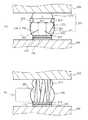
図6は、バンプクラックを引き起こす結晶粒界の一例と実施の形態1における半田バンプの結晶粒界の一例とを示す概念図である。
UBM層の結晶サイズや結晶方向の制御を特に行っていない従来の製法で製造された半田バンプ271では、図6(a)に示すように、半導体基板200側との接続箇所の端部320から側面部110までにおける外周面から半田バンプ271の径寸法Dの1/3の長さ以上に延びる結晶粒界が形成されてしまう。図6(a)では、半田バンプ271と半導体基板200側との接続箇所の端部320から延びる結晶粒界330が示されている。また、側面部110における外周面のある位置322から延びる結晶粒界332が示されている。また、側面部110における外周面のある位置324から延びる結晶粒界334が示されている。結晶粒界330,332,334は、いずれも半田バンプ271の径寸法Dの1/3の長さ以上に延びており、バンプクラックを引き起こす原因となる。フリップチップ接続後には、領域120に示す部分はパッケージ側の半田バンプと接続されてしまうため、露出した状態にはならないが、フリップチップ接続後にも露出した状態となる端部320から側面部110までにおける外周面から結晶粒界が延びるとそこを起点として亀裂が入りバンプクラックを引き起こす。特に、端部320付近は、熱変化による伸縮により応力集中が起こり、バンプクラックを引き起こしやすい箇所である。その際、バンプクラックが径寸法Dの1/3の長さ以上に延びると半田バンプ271の抵抗が1.33倍に上昇し、半導体業界で一般に許容される許容限界を超えてしまう。端部320から側面部110までにおける外周面から結晶粒界が径寸法Dの1/3の長さ以上に延びると、バンプクラックが生じた場合に径寸法Dの1/3の長さ以上まで伝播してしまうので、製造段階でこのような径寸法Dの1/3の長さ以上の結晶粒界を形成させないことが重要となる。
これに対し、実施の形態1における製造方法で製造された半田バンプ270では、図6(b)に示すように、半導体基板200側との接続箇所の端部112から側面部110までにおける外周面から半田バンプ270の径寸法Dの1/3の長さ以上に延びる結晶粒界が形成されない。これは、Cu膜260表面の凹凸を無くし、Cu膜260とSn膜262とを共に(111)配向にそろえたことにより、半田バンプ270の結晶粒界280の方向が半導体基板200面に略垂直な方向である略縦方向にそろったためである。なお、側面部110は、半導体基板200とパッケージ側の基板が接続した際に、半導体基板200側との接続箇所と領域120で示すパッケージ基板側との接続箇所とのいずれからも外れる半田バンプ270の外周面である。FIG. 6 is a conceptual diagram showing an example of a crystal grain boundary causing a bump crack and an example of a crystal grain boundary of a solder bump in the first embodiment.
In the
On the other hand, in the
以上のように、めっき前の下地膜となるCu膜240の結晶サイズと結晶方位とを制御することにより、Cu膜260表面の凹凸を無くし、Cu膜260とSn膜262とを共に(111)配向にそろえることができ、ひいては、半田バンプ270の結晶粒界280の方向を略縦方向にそろえることができる。その結果、許容限界を超えるバンプクラックを抑制することができる。 As described above, by controlling the crystal size and crystal orientation of the
図7は、図1のフローチャートに対応して実施される工程を表す工程断面図である。図7では、図1のフリップチップ接続工程(S124)を示している。 FIG. 7 is a process sectional view showing a process performed corresponding to the flowchart of FIG. FIG. 7 shows the flip chip connecting step (S124) of FIG.
図7において、フリップチップ接続工程(S124)として、半導体基板200とパッケージ基板300とをフリップチップ接続する。具体的には、半導体基板200側の半田バンプ270とパッケージ基板300側の半田バンプ272とを加熱して接続する。その結果、図7に示すようなフリップチップ接続された半導体装置が形成される。 In FIG. 7, as a flip chip connection step (S124), the
図8は、フリップチップ接続後におけるバンプクラックを引き起こす結晶粒界の一例と実施の形態1における半田バンプの結晶粒界の一例とを示す概念図である。
従来の製法で製造された半田バンプ271では、図8(a)に示すように、フリップチップ接続後において、半導体基板200側との接続箇所の端部320から側面部110までにおける外周面から半田バンプ271の径寸法Dの1/3の長さ以上に延びる結晶粒界が形成されてしまう。図8(a)では、半田バンプ271と半導体基板200側との接続箇所の端部320から延びる結晶粒界330が示されている。また、側面部110における外周面のある位置322から延びる結晶粒界332が示されている。また、側面部110における外周面のある位置324から延びる結晶粒界334が示されている。結晶粒界330,332,334は、いずれも半田バンプ271の径寸法Dの1/3の長さ以上に延びており、バンプクラックを引き起こす原因となる。フリップチップ接続後にも露出した状態となる端部320から側面部110までにおける外周面から結晶粒界が延びると上述したようにそこを起点として亀裂が入りバンプクラックを引き起こす。
これに対し、実施の形態1における製造方法で製造された半田バンプ270では、フリップチップ接続後において、図8(b)に示すように、半導体基板200側との接続箇所の端部112から側面部110までにおける外周面から半田バンプ270の径寸法Dの1/3の長さ以上に延びる結晶粒界が形成されない。これは、Cu膜260表面の凹凸を無くし、Cu膜260とSn膜262とを共に(111)配向にそろえたことにより、フリップチップ接続後においても半田バンプ270の結晶粒界282の方向が半導体基板200面に略垂直な方向である略縦方向にそろったためである。そして、パッケージ基板300側の半田バンプ272でも、フリップチップ接続後においては核となる結晶が半田バンプ270側に存在するため、半田バンプ270の結晶粒界282の方向に追従し、やはり、略縦方向にそろえることができる。FIG. 8 is a conceptual diagram showing an example of a crystal grain boundary that causes a bump crack after flip chip connection and an example of a crystal grain boundary of a solder bump in the first embodiment.
In the
On the other hand, in the
以上のように、フリップチップ接続後における半田バンプ270では、半導体基板200とパッケージ基板300との間に配置され、半導体基板200側との接続箇所とパッケージ基板300側との接続箇所から外れた外周面から半田バンプ270の径寸法Dの1/3の長さ以上に延びる結晶粒界が存在しない。すなわち、実施の形態1におけるフリップチップ接続後における半導体装置は、半導体基板200と、半導体基板200と接続するパッケージ基板300と、上述したような半田バンプ270とを備えている。かかる構成により、許容限界を超えるバンプクラックを抑制することができる。 As described above, the
また、図6(b)や図8(b)に示したような略縦方向に結晶粒がそろった半田バンプを用いた場合には、仮にクラックがストレス最大となる部分から発生したとしても、クラック進展が許容限界内に抑制される。さらに、最悪の場合、クラックが進展しても、略縦方向に割れるため、電気的な導通は保たれ、断線には至らない。従って、略縦方向に粒界がそろった半田バンプは2重の安全装置を備えているといえる。 In addition, when using solder bumps having crystal grains aligned substantially in the vertical direction as shown in FIG. 6B and FIG. 8B, even if cracks are generated from the portion where the stress is maximum, Crack growth is suppressed within acceptable limits. Furthermore, in the worst case, even if the crack progresses, it breaks in a substantially vertical direction, so that electrical conduction is maintained and disconnection does not occur. Therefore, it can be said that the solder bumps having grain boundaries aligned substantially in the vertical direction are provided with double safety devices.
実施の形態2.
実施の形態1では、下地膜となるCu膜240を形成した後、めっき法によりさらにCu膜260を形成する場合について説明したが、これに限るものではない。実施の形態2では、めっきを行わず、専らスパッタ法にて半田ボールバンプの材料の1つとなるCu膜を形成する場合について説明する。Embodiment 2. FIG.
In Embodiment 1, the case where the
図9は、実施の形態2における半導体装置の製造方法の要部を表すフローチャートである。図9において、Cu下地膜形成工程(S106)の代わりにCu膜形成工程(S107)を備えた点、Cuめっき工程(S112)を削除した点以外は、図1と同様である。Ti膜形成工程(S102)からNi膜形成工程(S104)までの各工程の内容は実施の形態1と同様である。 FIG. 9 is a flowchart showing a main part of the method of manufacturing a semiconductor device in the second embodiment. 9 is the same as FIG. 1 except that a Cu film forming step (S107) is provided instead of the Cu base film forming step (S106) and the Cu plating step (S112) is omitted. The contents of each process from the Ti film forming process (S102) to the Ni film forming process (S104) are the same as those in the first embodiment.
図10は、図9のフローチャートに対応して実施される工程を表す工程断面図である。図10では、図9のCu膜形成工程(S107)からTiエッチング工程(S120)までを示している。 FIG. 10 is a process sectional view showing a process performed corresponding to the flowchart of FIG. 9. FIG. 10 shows from the Cu film formation step (S107) to the Ti etching step (S120) in FIG.
図10(a)において、Cu膜形成工程(S107)として、Ni膜212上にスパッタ法を用いてCu膜242を例えば膜厚1μm形成する。Cu膜242は、半導体基板200側の半田バンプ形成プロセスにおけるUBM層の1つの層(第3の層)と半田ボールバンプの材料膜とを兼ねる。ここで、実施の形態2では、Cu膜242を形成する際に、実施の形態1と同様、Cu膜242の結晶サイズ(グレインサイズ)やCu膜242の配向性を制御する。Cu膜242を形成する際に、結晶サイズを平均が10μm以下になるように制御することと、Cu膜242が成長する際に最初に成膜される初期膜、例えば、膜厚の30%程度までの膜の結晶方位が(111)配向となる結晶がより多く含まれるように制御する点については、実施の形態1と同様である。そして、それらの制御方法も実施の形態1と同様である。当初のCu膜242の結晶方位が(111)配向以外の結晶を含んでいても、Cu膜242の成長に伴い、実施の形態1におけるCu膜260と同様、膜の成長に伴って、結晶方位を(111)配向に収束させることができる。そして、実施の形態1と同様のレジスト塗布工程(S108)とレジストパターン形成工程(S110)とを実施する。 In FIG. 10A, as a Cu film forming step (S107), a
図10(b)において、Snめっき工程(S114)として、開口部150底面に露出したCu膜242上にめっき法によりSn膜262を形成する(堆積させる)。その他の内容は実施の形態1と同様である。その後、実施の形態1と同様のレジスト除去工程(S116)とCu/Niエッチング工程(S118)とTiエッチング工程(S120)とを実施することで図10(c)に示す断面に形成することができる。ここで、Cu/Niエッチング工程(S118)において、実施の形態2では、実施の形態1よりもCu膜の膜厚が厚いので、エッチング液として、Sn膜262へのアタックを抑制した薬液を用いると好適である。具体的には、添加剤の入った過酸化水素水(H2O2)と酸との混合液を用いることができ、添加剤としては、例えば、EDTAのようなキレート剤を用いると好適である。そして、実施の形態1と同様のリフロー工程(S122)を実施することで、図5(c)及び図6(b)に示したように、実施の形態1と同様、半導体基板200側との接続箇所の端部112から側面部110までにおける外周面から半田バンプ270の径寸法Dの1/3の長さ以上に延びる結晶粒界が形成されない半田バンプ270を備えた半導体装置を製造することができる。また、実施の形態1と同様のフリップチップ接続工程(S124)を実施することで、図7及び図8(b)に示したように、実施の形態1と同様、半導体基板200側との接続箇所の端部112から側面部110までにおける外周面から半田バンプ270の径寸法Dの1/3の長さ以上に延びる結晶粒界が形成されない半田バンプ270を備えたフリップチップ接続後の半導体装置を製造することができる。In FIG. 10B, as the Sn plating step (S114), an
以上、具体例を参照しつつ実施の形態について説明した。しかし、本発明は、これらの具体例に限定されるものではない。例えば、半田バンプの材料として、SnCuを用いたが、これに限るものではなく、スズ−銀−銅(SnAgCu)、或いは、スズ−銀−銅−ニッケル(SnAgCuNi)を用いてもよい。SnAgCuの半田バンプを形成する場合には、Snめっきの代わりに、SnAgめっきを行えばよい。また、SnAgCuNiの半田バンプを形成する場合には、さらに、リフローする際に、Ni膜212まで溶融させた合金にすればよい。 The embodiments have been described above with reference to specific examples. However, the present invention is not limited to these specific examples. For example, SnCu is used as the material for the solder bumps, but is not limited thereto, and tin-silver-copper (SnAgCu) or tin-silver-copper-nickel (SnAgCuNi) may be used. When forming SnAgCu solder bumps, SnAg plating may be performed instead of Sn plating. Further, when forming SnAgCuNi solder bumps, an alloy melted up to the
また、電極のサイズ、形状、数などについても、半導体集積回路や各種の半導体素子において必要とされるものを適宜選択して用いることができる。 In addition, as to the size, shape, number, etc. of the electrodes, those required in the semiconductor integrated circuit and various semiconductor elements can be appropriately selected and used.
その他、本発明の要素を具備し、当業者が適宜設計変更しうる全ての半導体装置及び半導体装置の製造方法は、本発明の範囲に包含される。 In addition, all semiconductor devices and methods of manufacturing a semiconductor device that include elements of the present invention and that can be appropriately modified by those skilled in the art are included in the scope of the present invention.
また、説明の簡便化のために、半導体産業で通常用いられる手法、例えば、フォトリソグラフィプロセス、処理前後のクリーニング等は省略しているが、それらの手法が含まれ得ることは言うまでもない。 Further, for the sake of simplicity of explanation, techniques usually used in the semiconductor industry, such as a photolithography process, cleaning before and after processing, are omitted, but it goes without saying that these techniques may be included.
110 側面部、112,320 端部、200 半導体基板、240,242,260 Cu膜、262 Sn膜、270,272 半田バンプ、280,282,330,332,334 結晶粒界、300 パッケージ基板110 Side surface portion, 112, 320 edge portion, 200 Semiconductor substrate, 240, 242, 260 Cu film, 262 Sn film, 270, 272 Solder bump, 280, 282, 330, 332, 334 Grain boundary, 300 Package substrate
Claims (3)
Translated fromJapanese前記半導体基板上に形成され、前記半導体基板側との接続箇所の端部から側面部までにおける外周面から自己の径寸法の1/3の長さ以上に延びる結晶粒界が存在しない半田バンプ部と、
を備えたことを特徴とする半導体装置。A semiconductor substrate;
Solder bump portion formed on the semiconductor substrate and having no crystal grain boundary extending from the outer peripheral surface from the end portion to the side surface portion of the connection portion with the semiconductor substrate side to a length of 1/3 or more of its own radial dimension When,
A semiconductor device comprising:
前記半導体基板と接続する他の基板と、
前記半導体基板と前記他の基板との間に配置され、前記半導体基板側との接続箇所と前記他の基板側との接続箇所から外れた外周面から自己の径寸法の1/3の長さ以上に延びる結晶粒界が存在しない半田バンプ部と、
を備えたことを特徴とする半導体装置。
A semiconductor substrate;
Another substrate connected to the semiconductor substrate;
A length of 1/3 of its own radial dimension from an outer peripheral surface disposed between the semiconductor substrate and the other substrate and deviating from a connection location on the semiconductor substrate side and a connection location on the other substrate side. A solder bump portion where there is no crystal grain boundary extending above,
A semiconductor device comprising:
Priority Applications (2)
| Application Number | Priority Date | Filing Date | Title |
|---|---|---|---|
| JP2008221534AJP4987823B2 (en) | 2008-08-29 | 2008-08-29 | Semiconductor device |
| US12/497,371US8242597B2 (en) | 2008-08-29 | 2009-07-02 | Crystal structure of a solder bump of flip chip semiconductor device |
Applications Claiming Priority (1)
| Application Number | Priority Date | Filing Date | Title |
|---|---|---|---|
| JP2008221534AJP4987823B2 (en) | 2008-08-29 | 2008-08-29 | Semiconductor device |
Publications (2)
| Publication Number | Publication Date |
|---|---|
| JP2010056394A JP2010056394A (en) | 2010-03-11 |
| JP4987823B2true JP4987823B2 (en) | 2012-07-25 |
Family
ID=41724098
Family Applications (1)
| Application Number | Title | Priority Date | Filing Date |
|---|---|---|---|
| JP2008221534AExpired - Fee RelatedJP4987823B2 (en) | 2008-08-29 | 2008-08-29 | Semiconductor device |
Country Status (2)
| Country | Link |
|---|---|
| US (1) | US8242597B2 (en) |
| JP (1) | JP4987823B2 (en) |
Families Citing this family (12)
| Publication number | Priority date | Publication date | Assignee | Title |
|---|---|---|---|---|
| US9524945B2 (en)* | 2010-05-18 | 2016-12-20 | Taiwan Semiconductor Manufacturing Company, Ltd. | Cu pillar bump with L-shaped non-metal sidewall protection structure |
| US9067272B2 (en)* | 2010-06-18 | 2015-06-30 | Arizona Board Of Regents On Behalf Of Arizona State University | Systems and methods for high aspect ratio flip-chip interconnects |
| US10128206B2 (en)* | 2010-10-14 | 2018-11-13 | Taiwan Semiconductor Manufacturing Company, Ltd. | Conductive pillar structure |
| JP5779931B2 (en)* | 2011-03-24 | 2015-09-16 | 富士通株式会社 | Manufacturing method of semiconductor device |
| DE102011083926A1 (en)* | 2011-09-30 | 2013-04-04 | Robert Bosch Gmbh | Layer composite of a carrier film and a layer arrangement comprising a sinterable layer of at least one metal powder and a solder layer |
| TWI432613B (en)* | 2011-11-16 | 2014-04-01 | Univ Nat Chiao Tung | Electrodeposited nano-twins copper layer and method of fabricating the same |
| JP6011074B2 (en)* | 2012-01-20 | 2016-10-19 | 富士通株式会社 | Electronic device manufacturing method and electronic device manufacturing apparatus |
| TWI490962B (en)* | 2013-02-07 | 2015-07-01 | Univ Nat Chiao Tung | Electrical connecting element and method for manufacturing the same |
| JP6219227B2 (en) | 2014-05-12 | 2017-10-25 | 東京エレクトロン株式会社 | Heater feeding mechanism and stage temperature control method |
| US20170110392A1 (en)* | 2015-10-15 | 2017-04-20 | Advanced Semiconductor Engineering, Inc. | Semiconductor package structure and method for manufacturing the same structure |
| US9691723B2 (en)* | 2015-10-30 | 2017-06-27 | Taiwan Semiconductor Manufacturing Company, Ltd. | Connector formation methods and packaged semiconductor devices |
| WO2018077798A1 (en)* | 2016-10-24 | 2018-05-03 | Jaguar Land Rover Limited | Apparatus and method relating to electrochemical migration |
Family Cites Families (23)
| Publication number | Priority date | Publication date | Assignee | Title |
|---|---|---|---|---|
| US4976393A (en)* | 1986-12-26 | 1990-12-11 | Hitachi, Ltd. | Semiconductor device and production process thereof, as well as wire bonding device used therefor |
| DE69701277T2 (en)* | 1996-12-03 | 2000-08-31 | Lucent Technologies Inc., Murray Hill | Fine-particle soft solder containing dispersed particle article |
| JP3028791B2 (en)* | 1997-08-06 | 2000-04-04 | 日本電気株式会社 | How to mount chip components |
| US6205264B1 (en)* | 1998-04-14 | 2001-03-20 | Lucent Technologies Inc. | Optical assembly with improved dimensional stability |
| US7173336B2 (en)* | 2000-01-31 | 2007-02-06 | Sanyo Electric Co., Ltd. | Hybrid integrated circuit device |
| JP2003031576A (en)* | 2001-07-17 | 2003-01-31 | Nec Corp | Semiconductor element and manufacturing method therefor |
| JP3813497B2 (en)* | 2001-11-12 | 2006-08-23 | 株式会社ルネサステクノロジ | Bump forming method and semiconductor device mounting structure |
| US20040245648A1 (en)* | 2002-09-18 | 2004-12-09 | Hiroshi Nagasawa | Bonding material and bonding method |
| JP2004207685A (en)* | 2002-12-23 | 2004-07-22 | Samsung Electronics Co Ltd | Manufacturing method of lead-free solder bump |
| US7015590B2 (en)* | 2003-01-10 | 2006-03-21 | Samsung Electronics Co., Ltd. | Reinforced solder bump structure and method for forming a reinforced solder bump |
| CN1291069C (en)* | 2003-05-31 | 2006-12-20 | 香港科技大学 | Electroplating preparation method of fine-pitch flip-chip bumps |
| JP3764450B2 (en)* | 2003-07-28 | 2006-04-05 | Tdk株式会社 | Surface acoustic wave device, surface acoustic wave device, surface acoustic wave duplexer, and method of manufacturing surface acoustic wave device |
| WO2005016580A2 (en)* | 2003-08-06 | 2005-02-24 | Michigan State University | Composite metal matrix castings, solder compositions, and methods |
| US20060038302A1 (en)* | 2004-08-19 | 2006-02-23 | Kejun Zeng | Thermal fatigue resistant tin-lead-silver solder |
| KR100642765B1 (en)* | 2004-09-15 | 2006-11-10 | 삼성전자주식회사 | Microelectronic device chip comprising a hybrid bump, a package thereof, a liquid crystal display device comprising the same and a manufacturing method of such a microelectronic device chip |
| US7267861B2 (en)* | 2005-05-31 | 2007-09-11 | Texas Instruments Incorporated | Solder joints for copper metallization having reduced interfacial voids |
| US7601612B1 (en)* | 2005-10-24 | 2009-10-13 | Globalfoundries Inc. | Method for forming solder joints for a flip chip assembly |
| TWI330053B (en)* | 2006-08-14 | 2010-09-01 | Unimicron Technology Corp | Conductive connection structure formed on the surface of circuit board and manufacturing method thereof |
| US20080121903A1 (en)* | 2006-11-24 | 2008-05-29 | Sony Corporation | Method for manufacturing light-emitting diode, light-emitting diode, lightsource cell unit, light-emitting diode backlight, light-emitting diode illuminating device, light-emitting diode display, and electronic apparatus |
| JP5175476B2 (en)* | 2007-02-28 | 2013-04-03 | 三洋電機株式会社 | Circuit device manufacturing method |
| JP5138248B2 (en)* | 2007-03-23 | 2013-02-06 | オンセミコンダクター・トレーディング・リミテッド | Semiconductor device and manufacturing method thereof |
| US8552570B2 (en)* | 2008-01-09 | 2013-10-08 | Renesas Electronics Corporation | Wiring board, semiconductor device, and method for manufacturing wiring board and semiconductor device |
| US8493746B2 (en)* | 2009-02-12 | 2013-07-23 | International Business Machines Corporation | Additives for grain fragmentation in Pb-free Sn-based solder |
- 2008
- 2008-08-29JPJP2008221534Apatent/JP4987823B2/ennot_activeExpired - Fee Related
- 2009
- 2009-07-02USUS12/497,371patent/US8242597B2/enactiveActive
Also Published As
| Publication number | Publication date |
|---|---|
| US8242597B2 (en) | 2012-08-14 |
| JP2010056394A (en) | 2010-03-11 |
| US20100052162A1 (en) | 2010-03-04 |
Similar Documents
| Publication | Publication Date | Title |
|---|---|---|
| JP4987823B2 (en) | Semiconductor device | |
| TWI409892B (en) | Method of forming integrated circuit structures | |
| US11145619B2 (en) | Electrical connecting structure having nano-twins copper and method of forming the same | |
| CN103456704B (en) | The design at interval, connector site and the structure that obtains | |
| US9177827B2 (en) | Etchant and method for manufacturing semiconductor device using same | |
| TWI402925B (en) | Metal pillar bump structure and method for forming the same | |
| JPH10223608A (en) | Manufacture of semiconductor device | |
| CN1117655A (en) | Electroplated solder terminal | |
| US20060175686A1 (en) | Semiconductor device and fabrication method thereof | |
| US20070026670A1 (en) | Method of reducing contamination by removing an interlayer dielectric from the substrate edge | |
| JP2010093284A (en) | Method of manufacturing semiconductor device | |
| JP2010508673A (en) | Metallization layer stack without terminal aluminum metal layer | |
| JP2019169579A (en) | Semiconductor device and method of manufacturing the same | |
| US11121101B2 (en) | Flip chip packaging rework | |
| WO2016154315A1 (en) | Metal bond pad with cobalt interconnect layer and solder thereon | |
| US8426312B2 (en) | Method of reducing contamination by providing an etch stop layer at the substrate edge | |
| JP4493516B2 (en) | Manufacturing method of semiconductor device | |
| TW202310258A (en) | Electroplated indium bump stacks for cryogenic electronics | |
| US20020086512A1 (en) | Method of forming solder bumps | |
| TW201843776A (en) | Methods of forming integrated circuit structure for joining wafers and resulting structure | |
| TWI628774B (en) | Semiconductor device and method of manufacturing same | |
| JP2007251135A (en) | Semiconductor device and its manufacture | |
| US8318597B2 (en) | Manufacturing method of semiconductor device including Au bump on seed film | |
| US9461010B2 (en) | Debond interconnect structures | |
| WO2008054680A2 (en) | A metallization layer stack without a terminal aluminum metal layer |
Legal Events
| Date | Code | Title | Description |
|---|---|---|---|
| A621 | Written request for application examination | Free format text:JAPANESE INTERMEDIATE CODE: A621 Effective date:20100915 | |
| A977 | Report on retrieval | Free format text:JAPANESE INTERMEDIATE CODE: A971007 Effective date:20111228 | |
| A131 | Notification of reasons for refusal | Free format text:JAPANESE INTERMEDIATE CODE: A131 Effective date:20120110 | |
| A521 | Request for written amendment filed | Free format text:JAPANESE INTERMEDIATE CODE: A523 Effective date:20120301 | |
| TRDD | Decision of grant or rejection written | ||
| A01 | Written decision to grant a patent or to grant a registration (utility model) | Free format text:JAPANESE INTERMEDIATE CODE: A01 Effective date:20120403 | |
| A01 | Written decision to grant a patent or to grant a registration (utility model) | Free format text:JAPANESE INTERMEDIATE CODE: A01 | |
| A61 | First payment of annual fees (during grant procedure) | Free format text:JAPANESE INTERMEDIATE CODE: A61 Effective date:20120425 | |
| R151 | Written notification of patent or utility model registration | Ref document number:4987823 Country of ref document:JP Free format text:JAPANESE INTERMEDIATE CODE: R151 | |
| FPAY | Renewal fee payment (event date is renewal date of database) | Free format text:PAYMENT UNTIL: 20150511 Year of fee payment:3 | |
| S111 | Request for change of ownership or part of ownership | Free format text:JAPANESE INTERMEDIATE CODE: R313111 | |
| R350 | Written notification of registration of transfer | Free format text:JAPANESE INTERMEDIATE CODE: R350 | |
| S111 | Request for change of ownership or part of ownership | Free format text:JAPANESE INTERMEDIATE CODE: R313111 | |
| R350 | Written notification of registration of transfer | Free format text:JAPANESE INTERMEDIATE CODE: R350 | |
| LAPS | Cancellation because of no payment of annual fees |