JP4987301B2 - CMOS image sensor sharing sensing nodes of adjacent pixels - Google Patents
CMOS image sensor sharing sensing nodes of adjacent pixelsDownload PDFInfo
- Publication number
- JP4987301B2 JP4987301B2JP2006001285AJP2006001285AJP4987301B2JP 4987301 B2JP4987301 B2JP 4987301B2JP 2006001285 AJP2006001285 AJP 2006001285AJP 2006001285 AJP2006001285 AJP 2006001285AJP 4987301 B2JP4987301 B2JP 4987301B2
- Authority
- JP
- Japan
- Prior art keywords
- pixel
- sensing node
- image sensor
- cmos image
- scanned
- Prior art date
- Legal status (The legal status is an assumption and is not a legal conclusion. Google has not performed a legal analysis and makes no representation as to the accuracy of the status listed.)
- Active
Links
Images


Classifications
- H—ELECTRICITY
- H10—SEMICONDUCTOR DEVICES; ELECTRIC SOLID-STATE DEVICES NOT OTHERWISE PROVIDED FOR
- H10F—INORGANIC SEMICONDUCTOR DEVICES SENSITIVE TO INFRARED RADIATION, LIGHT, ELECTROMAGNETIC RADIATION OF SHORTER WAVELENGTH OR CORPUSCULAR RADIATION
- H10F39/00—Integrated devices, or assemblies of multiple devices, comprising at least one element covered by group H10F30/00, e.g. radiation detectors comprising photodiode arrays
- H10F39/80—Constructional details of image sensors
- H10F39/813—Electronic components shared by multiple pixels, e.g. one amplifier shared by two pixels
- H—ELECTRICITY
- H04—ELECTRIC COMMUNICATION TECHNIQUE
- H04N—PICTORIAL COMMUNICATION, e.g. TELEVISION
- H04N25/00—Circuitry of solid-state image sensors [SSIS]; Control thereof
- H—ELECTRICITY
- H04—ELECTRIC COMMUNICATION TECHNIQUE
- H04N—PICTORIAL COMMUNICATION, e.g. TELEVISION
- H04N25/00—Circuitry of solid-state image sensors [SSIS]; Control thereof
- H04N25/40—Extracting pixel data from image sensors by controlling scanning circuits, e.g. by modifying the number of pixels sampled or to be sampled
- H04N25/46—Extracting pixel data from image sensors by controlling scanning circuits, e.g. by modifying the number of pixels sampled or to be sampled by combining or binning pixels
- H—ELECTRICITY
- H04—ELECTRIC COMMUNICATION TECHNIQUE
- H04N—PICTORIAL COMMUNICATION, e.g. TELEVISION
- H04N25/00—Circuitry of solid-state image sensors [SSIS]; Control thereof
- H04N25/50—Control of the SSIS exposure
- H04N25/57—Control of the dynamic range
- H04N25/59—Control of the dynamic range by controlling the amount of charge storable in the pixel, e.g. modification of the charge conversion ratio of the floating node capacitance
- H—ELECTRICITY
- H04—ELECTRIC COMMUNICATION TECHNIQUE
- H04N—PICTORIAL COMMUNICATION, e.g. TELEVISION
- H04N25/00—Circuitry of solid-state image sensors [SSIS]; Control thereof
- H04N25/70—SSIS architectures; Circuits associated therewith
- H04N25/76—Addressed sensors, e.g. MOS or CMOS sensors
- H04N25/77—Pixel circuitry, e.g. memories, A/D converters, pixel amplifiers, shared circuits or shared components
- H—ELECTRICITY
- H10—SEMICONDUCTOR DEVICES; ELECTRIC SOLID-STATE DEVICES NOT OTHERWISE PROVIDED FOR
- H10F—INORGANIC SEMICONDUCTOR DEVICES SENSITIVE TO INFRARED RADIATION, LIGHT, ELECTROMAGNETIC RADIATION OF SHORTER WAVELENGTH OR CORPUSCULAR RADIATION
- H10F39/00—Integrated devices, or assemblies of multiple devices, comprising at least one element covered by group H10F30/00, e.g. radiation detectors comprising photodiode arrays
- H10F39/10—Integrated devices
- H10F39/12—Image sensors
- H10F39/18—Complementary metal-oxide-semiconductor [CMOS] image sensors; Photodiode array image sensors
Landscapes
- Engineering & Computer Science (AREA)
- Multimedia (AREA)
- Signal Processing (AREA)
- Solid State Image Pick-Up Elements (AREA)
- Transforming Light Signals Into Electric Signals (AREA)
Description
Translated fromJapanese本発明は、CMOS(Complementary Metal Oxide Semiconductor)イメージセンサに関し、特に、センシングノードの貯蔵容量を増大させることができるCMOSイメージセンサの画素アレイ(pixel array)に関する。 The present invention relates to a complementary metal oxide semiconductor (CMOS) image sensor, and more particularly to a pixel array of a CMOS image sensor that can increase the storage capacity of a sensing node.
一般に、イメージセンサとは、光に反応する半導体の性質(光電変換)を用いて、イメージを捕捉する(capture)装置(素子)である。自然に存在する被写体の各部分は、光の強度(明るさ)及び波長が相互に異なっており、これを感知するイメージセンサの各画素では異なる電気的な値を生成するが、この電気的な値を信号処理が可能なレベルにすることがイメージセンサの役割である。 In general, an image sensor is a device (element) that captures an image using the property (photoelectric conversion) of a semiconductor that reacts to light. Each part of a naturally occurring subject has a different light intensity (brightness) and wavelength, and each pixel of an image sensor that senses this generates a different electrical value. It is the role of the image sensor to set the value to a level that allows signal processing.
図1は、通常のCMOSイメージセンサに関する構成を示すブロック図である。CMOSイメージセンサは、CMOSイメージセンサの全体的な動作を制御し、外部システムに対するインターフェース(interface)の役割を担う制御及び外部システムインターフェース部10、光に反応する性質を極大化させるように形成された画素が横N個、縦M個にアレイ状に配置されて外部から入るイメージに関する情報、即ち光を感知する画素アレイ部20、センサの各画素で生成されたアナログ電圧をデジタルシステムで処理が可能になるように、デジタル電圧に変換するアナログ−デジタル変換器(Analog-digital converter)30、及び、アナログ−デジタル変換器30の出力に応答し、デジタル化された画素のイメージ信号値をデジタルデータとして貯蔵するバッファ40を備えている。そして、アナログ−デジタル変換器30は、各画素で感知した電圧と比べるのに用いられる、クロックによって線形的に減少するランプ(ramp)状の比較基準電圧を作り出すデジタル−アナログ変換器(Digital-Analog converter、以下、DACという)31及び画素アレイ20から出力される感知電圧(アナログ電圧)とDAC31から出力される比較基準電圧とを比べ、比較基準電圧が画素電圧よりも大きい間、制御及び外部システムインターフェース部10から出力されるカウンタ値をバッファ40に書き込み可能にする書き込み可能信号を出力するN個の配列で構成された電圧比較器32を備えている。 FIG. 1 is a block diagram showing a configuration related to a normal CMOS image sensor. The CMOS image sensor is formed to control the overall operation of the CMOS image sensor and maximize the property of reacting to the control and external
上記のような構成のCMOSイメージセンサが高画質のイメージ生成のために相互関連された二重サンプリング方式(correlated double sampling method、以下、CDSという)を採用する場合、図2に示されているように、画素アレイのうち、それぞれの単位画素100、120は、1個のフォトダイオードと4個のトランジスタとでそれぞれ構成される。4個のトランジスタは、フォトダイオード101によって生成された光電荷をセンシングノードAに伝送するトランスファートランジスタM21と、次の信号検出のためにセンシングノードAに貯蔵されている電荷を排出するリセットトランジスタM11と、ソースフォロワー(source follower)の役割を担うドライブトランジスタM31と、スイッチングによってアドレッシングを可能とするセレクトトランジスタM41とである。 When the CMOS image sensor having the above configuration adopts a correlated double sampling method (hereinafter referred to as CDS) for generating a high-quality image, as shown in FIG. In addition, in the pixel array, each
ここで、CDSとは、単位画素を構成するリセットトランジスタM11をターン−オン(turn-on)、トランスファートランジスタM21をターン−オフ(turn-off)させて、リセット時の電圧(リセット電圧)を取得し、その次に、リセットトランジスタM11をターン−オフさせた状態でトランスファートランジスタM21をターン−オンさせて、フォトダイオード101によって生成された電荷を読み出し、これによる電圧(データ電圧)を取得した後、リセット電圧とデータ電圧との差を純粋なイメージデータとして採用する方式を意味する。 Here, CDS is a reset transistor M11 constituting a unit pixel, which is turned on, and a transfer transistor M21 is turned off, thereby obtaining a reset voltage (reset voltage). Then, the transfer transistor M21 is turned on with the reset transistor M11 turned off, the charge generated by the
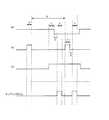
図3は、図2の単位画素構成で各トランジスタを制御する信号に関する制御タイミングを示すタイミングチャートである。これを参照して単位画素100の動作を期間毎に説明する。 FIG. 3 is a timing chart showing control timings related to signals for controlling each transistor in the unit pixel configuration of FIG. The operation of the
1)図3において、「A」期間は、トランスファートランジスタM21及びリセットトランジスタM11がターン−オンされ、セレクトトランジスタM41がターン−オフされて、フォトダイオード101を完全に空乏(fully depletion)させる期間である。 1) In FIG. 3, a period “A” is a period in which the transfer transistor M21 and the reset transistor M11 are turned on, and the select transistor M41 is turned off, thereby causing the
2)「B」期間は、ターン−オンされたトランスファートランジスタM21が再びターン−オフされることによって、フォトダイオード101で光を吸収して光電荷を生成し、生成された光電荷を集積する期間である。(「B」期間は、リセットトランジスタM11及びセレクトトランジスタM41の状態と関係なしに、トランスファートランジスタM21が再びターン−オンされるまで維持される。)
3)「C」期間は、リセットトランジスタM11がターン−オン状態、トランスファートランジスタM21がターン−オフ状態に続けて維持され、セレクトトランジスタM41がターン−オンされることによって、センシングノードAにより駆動されるドライブトランジスタM31及びセレクトトランジスタM41を介してリセット電圧レベルを伝達する期間である。(reset level transfer 期間)
4)「D」期間は、リセットトランジスタM11がターン−オフされることによって、「C」期間で発生したリセット電圧レベルを安定させる期間である。(reset level settling 期間)
5)「E」期間は、「D」期間からのリセット電圧をサンプリングする期間である。(reset level sampling 期間)
6)「F」期間は、リセットトランジスタM11及びセレクトトランジスタM41がそれぞれターン−オフ、ターン−オン状態に維持され、トランスファートランジスタM21がターン−オンされることによって、「B」期間の間フォトダイオード101で集積された光電荷によるデータ電圧がセンシングノードAに伝達されてセンシングノードAにより駆動されるドライブトランジスタM31及びセレクトトランジスタM41により、データ電圧を伝達する期間である。(data level transfer 期間)
7)「G」期間は、トランスファートランジスタM21がターン−オフされることによって、「F」期間で発生したデータ電圧を安定させる期間である。(data level settling 期間)
8)「H」期間は、「G」期間のデータ電圧をサンプリングする期間である。(data level sampling 期間)
「E」期間及び「H」期間でそれぞれサンプリングされるリセット電圧及びデータ電圧は、図1のアナログ−デジタル変換器30に出力されてデジタル信号に変換され、デジタル信号に変換されたそれら2つの電圧値の差が、フォトダイオード101から受け取ったイメージに対するCMOSイメージセンサの出力イメージ値(イメージデータ)になる。2) In the “B” period, the transfer transistor M21 that has been turned on is turned off again, so that the
3) During the “C” period, the reset transistor M11 is maintained in the turn-on state, the transfer transistor M21 is maintained in the turn-off state, and the select transistor M41 is turned on to be driven by the sensing node A. This is a period during which the reset voltage level is transmitted via the drive transistor M31 and the select transistor M41. (Reset level transfer period)
4) The “D” period is a period in which the reset voltage level generated in the “C” period is stabilized when the reset transistor M11 is turned off. (Reset level settling period)
5) The “E” period is a period for sampling the reset voltage from the “D” period. (Reset level sampling period)
6) In the “F” period, the reset transistor M11 and the select transistor M41 are maintained in the turn-off and turn-on states, respectively, and the transfer transistor M21 is turned on, so that the
7) The “G” period is a period in which the data voltage generated in the “F” period is stabilized when the transfer transistor M21 is turned off. (Data level settling period)
8) The “H” period is a period for sampling the data voltage of the “G” period. (Data level sampling period)
The reset voltage and data voltage sampled in the “E” period and “H” period, respectively, are output to the analog-to-
上述したような従来の単位画素100動作は、他の全ての単位画素においても同様に行われ、このような単位画素がアレイ状に配列されている画素アレイの駆動は、ロー(row:「行」とも記す)ベーススキャン方式を採択した場合、最初のローから最後のローまで順次スキャンされることになる。 The operation of the
したがって、例えば、n−1番目のローの画素からデータを得た後、n番目のローからデータを得る時、n−1番目を含むそれ以前のローに該当するピクセルは、クリーン−アップ(clean-up)された後、再び光の集積(integration)を行うことになる。 Thus, for example, when data is obtained from the pixel of the (n-1) th row and then data is obtained from the nth row, the pixels corresponding to the previous rows including the (n-1) th row are cleaned up. -up), the light integration will be performed again.
一方、上述したように、各単位画素を構成しているフォトダイオードは、光電荷を生成及び集積する容量が大きければ、より良いイメージデータを得ることができるので、このために、フォトダイオードの面積を増大させる等の技術によってフィル−ファクター(fill-factor)を改善している。 On the other hand, as described above, the photodiode constituting each unit pixel can obtain better image data if the capacitance for generating and integrating the photocharge is large. The fill factor is improved by a technique such as increasing the fill factor.
しかし、高濃度不純物の拡散領域によって具現されるセンシングノードに関しては、フィル−ファクターの改善により増大した光電荷を十分に受け取ることができる容量にすることができず、所望の光感度を得ることができないという問題がある。 However, regarding the sensing node embodied by the diffusion region of the high concentration impurity, it is not possible to obtain a capacity capable of sufficiently receiving the photocharge increased by the improvement of the fill factor, and a desired photosensitivity can be obtained. There is a problem that you can not.
本発明は、上述した従来の問題点を解決するためになされたものであって、その目的は、改善されたフィル−ファクターにより生成されたより多い光電荷をセンシングノードで受け取ることができるようにするために、選択された特定の画素が動作する時に、非選択の隣接する他の画素のセンシングノードを共有することによって、センシングノードの電荷貯蔵容量を増大させたCMOSイメージセンサを提供することにある。 The present invention has been made to solve the above-mentioned conventional problems, and its purpose is to allow the sensing node to receive more photocharge generated by the improved fill factor. Therefore, it is to provide a CMOS image sensor in which a charge storage capacity of a sensing node is increased by sharing a sensing node of another non-selected adjacent pixel when a selected specific pixel operates. .
上記の目的を達成するために、本発明の第1のCMOSイメージセンサは、ロー及びカラム方向にマトリックス状に配列された複数の単位画素を含む画素アレイを備え、各単位画素が、外部の光を吸収して光電荷を生成するフォトダイオードと、該フォトダイオードから光電荷を受け取るセンシングノードと、を備え、現在スキャンしているラインのライン選択信号に応答して、現在スキャン中であるラインの第1画素の第1センシングノードと、1つ前のスキャンでスキャンされたラインの第2画素の第2センシングノードとが、一体として、現在スキャン中であるラインの前記第1画素のフォトダイオードからのみ光電荷を受け取ることを特徴としている。In order to achieve the above object, a first CMOS image sensor of the present invention includes a pixel array including a plurality of unit pixels arranged in a matrix in the row and column directions, and each unit pixel has an external light. And a sensing node for receiving photocharge from the photodiode, and in response to a line selection signal of the line currently scanned, The firstsensing node of the first pixel and the second sensing node of the second pixel of the line scanned in the previous scan are integrally formed from the photodiode of the first pixel of the line currently being scanned. It is characterized by only receiving photocharges.
また、本発明の第2のCMOSイメージセンサは、ロー及びカラム方向にマトリックス状に配列された複数の単位画素を含む画素アレイと、選択信号に応答し、この信号により選択された第1画素の第1センシングノードと前記第1画素に隣接する選択されていない第2画素の第2センシングノードとを相互接続するスイッチング素子と、を備え、各単位画素が、外部の光を吸収して光電荷を生成するフォトダイオードと、該フォトダイオードから光電荷を受け取るセンシングノードと、前記第1画素のフォトダイオードからのみ光電荷を前記センシングノードに伝達するトランスファートランジスタと、前記センシングノードをリセットさせるリセットトランジスタと、前記センシングノードに貯蔵される電荷量に対応する電気的信号を出力する出力部と、一側が前記出力部に接続し、選択信号に応答してスイッチングしてアドレッシングを行うセレクトトランジスタと、を含むことを特徴としている。
さらに、本発明の第3のCMOSイメージセンサは、複数の単位画素を有する画素アレイと、第1画素の第1センシングノードを、現在スキャンしていない第2画素の第2センシングノードと相互接続するスイッチング素子と、を備え、前記各単位画素が、外部の光を吸収して光電荷を生成するフォトダイオードと、前記第1画素のフォトダイオードからのみ光電荷を前記センシングノードに伝達するトランスファートランジスタと、前記センシングノードをリセットさせるリセットトランジスタと、前記センシングノードに貯蔵される電荷量に対応する電気的信号を出力する出力部と、一側が前記出力部に接続するセレクトトランジスタと、を備えたことを特徴としている。The second CMOS image sensor of the present invention includes a pixel array including a plurality of unit pixels arranged in a matrix in the row and column directions, and a first pixel selected by this signal in response to a selection signal. A switching element interconnecting the first sensing node and the second sensing node of the second pixelthat is not selected and adjacent to the first pixel, and each unit pixel absorbs external light to generate a photocharge A sensing node that receives photocharge fromthe photodiode, a transfer transistor that transmits photochargeonly fromthe photodiode ofthe first pixel tothe sensing node, and a reset transistor that resets the sensing node An electrical signal corresponding to the amount of charge stored in the sensing node. An output unit for, is characterized in that one side is connected to the output section, including a select transistor for addressing and switching in response to the selection signal.
Furthermore, a third CMOS image sensor of the present invention interconnects a pixel array having a plurality of unit pixels and a first sensing node of the first pixel with a second sensing node of a second pixel that is not currently scanned. A switching element, wherein each unit pixel absorbs external light to generate photoelectric charge, and a transfer transistor transmits photoelectric charge only from the photodiode of the first pixel to the sensing node. A reset transistor that resets the sensing node; an output unit that outputs an electrical signal corresponding to an amount of charge stored in the sensing node; and a select transistor that is connected to the output unit on one side. It is a feature.
本発明のCMOSイメージセンサによれば、選択されたラインの特定の画素が動作する時、非選択のラインの隣接する別の画素のセンシングノードを共有することによって、改善されたフィル−ファクターにより生成されたより多い光電荷をセンシングノードで受け取ることができるようにする。すなわち、隣接画素間のセンシングノードの共有によりセンシングノードの電荷貯蔵容量を増大させ、高品質、高画質のCMOSイメージセンサの具現が可能となる。 According to the CMOS image sensor of the present invention, when a specific pixel of a selected line operates, it is generated with an improved fill factor by sharing a sensing node of another pixel adjacent to the non-selected line. So that more photo charge generated can be received at the sensing node. That is, by sharing the sensing node between adjacent pixels, the charge storage capacity of the sensing node is increased, and a high-quality, high-quality CMOS image sensor can be realized.
以下、本発明のもっとも好ましい実施の形態を添付する図面を参照して説明する。 The most preferred embodiments of the present invention will be described below with reference to the accompanying drawings.
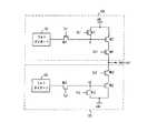
図4は、本発明の実施の形態に係るCMOSイメージセンサの画素アレイの構成の一部を示す回路図であって、複数の単位画素がロー及びカラム方向にマトリックス状に配列された画素アレイの中から、同じカラム上で隣り合っている3個の単位画素を示したものである。 FIG. 4 is a circuit diagram showing a part of the configuration of the pixel array of the CMOS image sensor according to the embodiment of the present invention. The pixel array includes a plurality of unit pixels arranged in a matrix in the row and column directions. From the inside, three unit pixels adjacent to each other on the same column are shown.
本実施の形態に係るCMOSイメージセンサでは、従来の構成と同様に、複数の単位画素がロー及びカラム方向にマトリックス状に配列されて画素アレイを構成しており、画素アレイのいずれかのライン(ローまたはカラム)に沿って、順次信号を読み出す処理(スキャン)が行われるラインスキャン方式で駆動する。本実施の形態が従来の技術と異なる点は、現在スキャン中であるライン(例えば、図4のn行)の画素のセンシングノード(例えば、図4のセンシングノードSN2)は、1つ前のスキャンでスキャンされたラインの画素のセンシングノード(例えば、図4のセンシングノードSN1)と共に、現在スキャン中であるラインの画素のフォトダイオード(例えば、図4のフォトダイオードPD2)から光電荷を受け取ることである。この2つのセンシングノードが共に用いられることを、センシングノードの共有とも記す。 In the CMOS image sensor according to the present embodiment, a plurality of unit pixels are arranged in a matrix in the row and column directions to form a pixel array, as in the conventional configuration, and any line ( The signal is driven by a line scan method in which a process (scan) for sequentially reading out signals along a row or a column is performed. This embodiment is different from the conventional technique in that the sensing node (for example, sensing node SN2 in FIG. 4) of the pixel currently being scanned (for example, the nth row in FIG. 4) scans the previous scan. In addition to the pixel sensing node (eg, sensing node SN1 in FIG. 4) scanned in line, the photocharge is received from the pixel photodiode (eg, photodiode PD2 in FIG. 4) currently being scanned. is there. The fact that these two sensing nodes are used together is also referred to as sensing node sharing.
図4は、ラインスキャン方式がローベーススキャン方式である場合の実施の形態であり、センシングノード間の共有は、同じカラム上の最隣接画素間で行われる。仮に、ラインスキャン方式がカラムベーススキャン方式であれば、センシングノード間の共有は、同じロー上の最隣接画素間で行われるようにする。 FIG. 4 shows an embodiment in which the line scan method is a low-base scan method, and sharing between sensing nodes is performed between adjacent pixels on the same column. If the line scan method is a column-based scan method, sharing between sensing nodes is performed between the adjacent pixels on the same row.
ライン選択信号に制御されて隣接する画素のセンシングノードを接続するスイッチング素子によりセンシングノードの共有が具現され、このために、図4の実施の形態において、スイッチング素子は、選択された画素のセンシングノードSN2と隣接する別の画素のセンシングノードSN1との間にソース−ドレイン経路が接続され、ゲートに現在スキャン中であるローのロー選択信号Sx2が入力されるNMOSトランジスタM400として具現されている。 The sharing of the sensing node is realized by the switching element connected to the sensing node of the adjacent pixel controlled by the line selection signal. For this reason, in the embodiment of FIG. 4, the switching element is the sensing node of the selected pixel. A source-drain path is connected between SN2 and a sensing node SN1 of another adjacent pixel, and is implemented as an NMOS transistor M400 in which a low row selection signal Sx2 currently being scanned is input to the gate.
図4に示した本発明の実施の形態に係るCMOSイメージセンサをより詳細に説明する。 The CMOS image sensor according to the embodiment of the present invention shown in FIG. 4 will be described in more detail.
図4は、ロースキャン方式を採用した場合の回路図であって、n−1行、n行及びn+1行の3つのローといずれかのカラムに対応する3個の単位画素だけを示したものである。 FIG. 4 is a circuit diagram in the case of adopting the row scan method, and shows only three unit pixels corresponding to three rows and one column of n−1 rows, n rows, and n + 1 rows. It is.
n行の単位画素に対する構成を説明すると、n行の単位画素は、外部の光を吸収して光電荷を生成する光電荷生成部PD2と、光電荷生成部PD2から光電荷を受け取るセンシングノードSN2と、光電荷生成部PD2からの光電荷をセンシングノードSN2に伝達する伝達部M421と、センシングノードSN2をリセットさせるリセット部M422と、センシングノードSN2に対応する電気的信号を出力する出力部M423、及び一側が出力部M423に接続され、ロー選択信号Sx2に応答し、スイッチングの役割をしてアドレッシングを行うアドレッシング部M424を備えている。光電荷生成部PD2は、フォトダイオードで構成されており、アドレッシング部M424は、一側が出力部に接続し、他側が出力端(output line)に接続するNMOSトランジスタで構成されており、出力部は、一側が第1電源端Vccに接続し、他側がアドレッシング部M424の一側に接続するNMOSトランジスタで構成されており、リセット部M422は、一側が第1電源端Vccに接続し、他側がセンシングノードに接続するNMOSトランジスタで構成されており、伝達部M421は、一側が光電荷生成部PD2に接続し、他側がセンシングノードSN2に接続するNMOSトランジスタで構成されている。 The configuration of the n-row unit pixel will be described. The n-row unit pixel absorbs external light to generate a photocharge, and a sensing node SN2 that receives the photocharge from the photocharge generation unit PD2. A transmission unit M421 that transmits the photocharge from the photocharge generation unit PD2 to the sensing node SN2, a reset unit M422 that resets the sensing node SN2, and an output unit M423 that outputs an electrical signal corresponding to the sensing node SN2. And one side is connected to the output unit M423, and includes an addressing unit M424 that performs switching and performs addressing in response to the row selection signal Sx2. The photocharge generator PD2 is configured by a photodiode, and the addressing unit M424 is configured by an NMOS transistor having one side connected to the output unit and the other side connected to an output line (output line). The one side is connected to the first power supply terminal Vcc and the other side is connected to one side of the addressing unit M424. The reset unit M422 has one side connected to the first power supply terminal Vcc and the other side sensing. The transmission unit M421 is configured by an NMOS transistor having one side connected to the photoelectric charge generation unit PD2 and the other side connected to the sensing node SN2.
n−1行及びn+1行の単位画素も実質的に同じ構成を有する。 The unit pixels in the (n−1) th row and the (n + 1) th row have substantially the same configuration.
さらに、本実施の形態に係るCMOSイメージセンサは、選択された画素に対するセンシングノードの貯蔵容量を増大させるために、ロー選択信号に応答して、前にスキャンされた隣接した別の画素のセンシングノードと選択された画素のセンシングノードとを相互接続するスイッチング素子M400、M450を備えている。具体的には、スイッチング素子は、選択された画素のセンシングノードSN2と隣接する別の画素のセンシングノードSN1との間にソース−ドレイン経路が形成され、ゲートにロー選択信号が入力されるNMOSトランジスタとして構成されている。 In addition, the CMOS image sensor according to the present embodiment can detect the sensing node of another adjacent pixel previously scanned in response to the row selection signal in order to increase the storage capacity of the sensing node for the selected pixel. And switching elements M400 and M450 that interconnect the sensing nodes of the selected pixels. Specifically, the switching element includes an NMOS transistor in which a source-drain path is formed between a sensing node SN2 of a selected pixel and a sensing node SN1 of another adjacent pixel, and a low selection signal is input to a gate. It is configured as.
例えば、n行の画素が選択されてスキャンされていると、1つ前にスキャンされたn−1行の画素のセンシングノードSN1とn行の画素のセンシングノードSN2とが共有されて、n行の画素のフォトダイオードPD2から光電荷を受け取る。 For example, when n rows of pixels are selected and scanned, the sensing node SN1 of the n−1 row pixels scanned the previous time and the sensing node SN2 of the n rows of pixels are shared, and n rows The photoelectric charge is received from the photodiode PD2 of the pixel.
その結果、改善されたフィル−ファクターにより生成されたより多い光電荷をセンシングノードで十分に受け取ることができる。 As a result, more photocharge generated by the improved fill factor can be fully received at the sensing node.
尚、本発明は、上記の実施の形態に限定されるものではなく、本発明に係る技術的思想から逸脱しない範囲内で様々な変更が可能であり、それらも本発明の技術的範囲に属する。 The present invention is not limited to the above-described embodiments, and various modifications are possible without departing from the technical idea according to the present invention, and these also belong to the technical scope of the present invention. .
Claims (18)
Translated fromJapanese各単位画素が、
外部の光を吸収して光電荷を生成するフォトダイオードと、
該フォトダイオードから光電荷を受け取るセンシングノードと、を備え、
現在スキャンしているラインのライン選択信号に応答して、現在スキャン中であるラインの第1画素の第1センシングノードと、1つ前のスキャンでスキャンされたラインの第2画素の第2センシングノードとが、一体として、現在スキャン中であるラインの前記第1画素のフォトダイオードからのみ光電荷を受け取ることを特徴とするCMOSイメージセンサ。A pixel array including a plurality of unit pixels arranged in a matrix in the row and column directions,
Each unit pixel is
A photodiode that absorbs external light and generates a photocharge;
A sensing node for receiving photocharge from the photodiode;
In response to the line selection signal of the currently scanned line,the first sensing node of the first pixel ofthe line currently being scannedand the second sensing of the second pixel of the line scanned in the previous scan A CMOS image sensor characterized in that a node receives light charges only from a photodiode of the first pixel of a line currently being scannedas a unit .
現在スキャン中であるローの前記第1画素の前記第1センシングノードが、1つ前にスキャンされたローの前記第2画素の前記第2センシングノードと共に、現在スキャン中であるローの前記第1画素の前記フォトダイオードからのみ光電荷を受け取ることを特徴とする請求項1に記載のCMOSイメージセンサ。The line scan method is a low-base scan method,
The first sensing node of the first pixel of the row currently being scanned, together with the second sensing node of the second pixel of the previously scanned row, the first of the row currently being scanned 2. The CMOS image sensor according to claim 1, wherein photoelectric charge is received only from the photodiode of the pixel.
現在スキャン中であるカラムの前記第1画素の前記第1センシングノードが、1つ前にスキャンされたカラムの前記第2画素の前記第2センシングノードと共に、現在スキャン中であるカラムの前記第1画素の前記フォトダイオードからのみ光電荷を受け取ることを特徴とする請求項1に記載のCMOSイメージセンサ。The line scan method is a column-based scan method,
The first sensing node of the first pixel of the column currently being scanned, together with the second sensing node of the second pixel of the column scanned last time, the first sensing node of the column currently being scanned 2. The CMOS image sensor according to claim 1, wherein photoelectric charge is received only from the photodiode of the pixel.
選択信号に応答し、この信号により選択された第1画素の第1センシングノードと、前記第1画素に隣接する選択されていない第2画素の第2センシングノードとを相互接続するスイッチング素子と、を備え、
各単位画素が、
外部の光を吸収して光電荷を生成するフォトダイオードと、
該フォトダイオードから光電荷を受け取るセンシングノードと、
前記第1画素のフォトダイオードからのみ光電荷を前記センシングノードに伝達するトランスファートランジスタと、
前記センシングノードをリセットさせるリセットトランジスタと、
前記センシングノードに貯蔵される電荷量に対応する電気的信号を出力する出力部と、
一側が前記出力部に接続し、選択信号に応答してスイッチングしてアドレッシングを行うセレクトトランジスタと、を含むことを特徴とするCMOSイメージセンサ。A pixel array including a plurality of unit pixels arranged in a matrix in the row and column directions;
A switching element that is responsive to a selection signal and interconnects the first sensing node of the first pixel selected by the signal and the second sensing node of the unselected second pixel adjacent to the first pixel; With
Each unit pixel is
A photodiode that absorbs external light and generates a photocharge;
A sensing node for receiving photocharge from the photodiode;
A transfer transistor that transmits photocharge to the sensing node only from the photodiode of the first pixel;
A reset transistor for resetting the sensing node;
An output unit for outputting an electrical signal corresponding to the amount of charge stored in the sensing node;
A CMOS image sensor comprising: a select transistor connected on one side to the output unit, and performing switching and addressing in response to a selection signal.
前記第1及び前記第2画素が、同じカラム上の最隣接する画素であることを特徴とする請求項7に記載のCMOSイメージセンサ。The pixel array is driven by a low-base scan method;
8. The CMOS image sensor according to claim 7, wherein the first and second pixels are adjacent pixels on the same column.
前記第1及び前記第2画素が、同じロー上の最隣接する画素であることを特徴とする請求項7に記載のCMOSイメージセンサ。The pixel array is driven by a column-based scan method,
8. The CMOS image sensor according to claim 7, wherein the first and second pixels are adjacent pixels on the same row.
一側が前記出力部に接続し、他側が出力端に接続するNMOSトランジスタで構成されることを特徴とする請求項7に記載のCMOSイメージセンサ。The select transistor is
8. The CMOS image sensor according to claim 7, comprising an NMOS transistor having one side connected to the output unit and the other side connected to the output terminal.
一側が第1電源端に接続し、他側が前記セレクトトランジスタの一側に接続するNMOSトランジスタで構成されることを特徴とする請求項7に記載のCMOSイメージセンサ。The output unit is
8. The CMOS image sensor according to claim 7, further comprising an NMOS transistor having one side connected to the first power supply terminal and the other side connected to one side of the select transistor.
一側が第1電源端に接続し、他側が前記センシングノードに接続するNMOSトランジスタで構成されることを特徴とする請求項7に記載のCMOSイメージセンサ。The reset transistor is
8. The CMOS image sensor according to claim 7, further comprising an NMOS transistor having one side connected to the first power supply terminal and the other side connected to the sensing node.
現在スキャン中である第1画素の第1センシングノードを、現在スキャンしていない第2画素の第2センシングノードと相互接続するスイッチング素子と、を備え、
前記各単位画素が、
外部の光を吸収して光電荷を生成するフォトダイオードと、
前記第1画素のフォトダイオードからのみ光電荷を前記センシングノードに伝達するトランスファートランジスタと、
前記センシングノードをリセットさせるリセットトランジスタと、
前記センシングノードに貯蔵される電荷量に対応する電気的信号を出力する出力部と、
一側が前記出力部に接続するセレクトトランジスタと、を備えたことを特徴とするCMOSイメージセンサ。A pixel array having a plurality of unit pixels;
A switching element interconnecting the first sensing node of the first pixel currently being scanned with the second sensing node of the second pixel not currently being scanned,
Each unit pixel is
A photodiode that absorbs external light and generates a photocharge;
A transfer transistor that transmits photocharge to the sensing node only from the photodiode of the first pixel;
A reset transistor for resetting the sensing node;
An output unit for outputting an electrical signal corresponding to the amount of charge stored in the sensing node;
A CMOS image sensor, comprising: a select transistor connected on one side to the output unit.
Applications Claiming Priority (2)
| Application Number | Priority Date | Filing Date | Title |
|---|---|---|---|
| KR10-2005-0008654 | 2005-01-31 | ||
| KR1020050008654AKR100680469B1 (en) | 2005-01-31 | 2005-01-31 | CMOS image sensor with sensing nodes shared between adjacent pixels |
Publications (2)
| Publication Number | Publication Date |
|---|---|
| JP2006211653A JP2006211653A (en) | 2006-08-10 |
| JP4987301B2true JP4987301B2 (en) | 2012-07-25 |
Family
ID=36756096
Family Applications (1)
| Application Number | Title | Priority Date | Filing Date |
|---|---|---|---|
| JP2006001285AActiveJP4987301B2 (en) | 2005-01-31 | 2006-01-06 | CMOS image sensor sharing sensing nodes of adjacent pixels |
Country Status (3)
| Country | Link |
|---|---|
| US (4) | US8149312B2 (en) |
| JP (1) | JP4987301B2 (en) |
| KR (1) | KR100680469B1 (en) |
Families Citing this family (18)
| Publication number | Priority date | Publication date | Assignee | Title |
|---|---|---|---|---|
| US7705900B2 (en)* | 2005-06-01 | 2010-04-27 | Eastman Kodak Company | CMOS image sensor pixel with selectable binning and conversion gain |
| KR100790582B1 (en)* | 2006-10-16 | 2008-01-02 | (주) 픽셀플러스 | CMOS image sensor pixel |
| KR100790583B1 (en)* | 2006-10-16 | 2008-01-02 | (주) 픽셀플러스 | CMOS image sensor shared pixel |
| US7924333B2 (en) | 2007-08-17 | 2011-04-12 | Aptina Imaging Corporation | Method and apparatus providing shared pixel straight gate architecture |
| US7989749B2 (en)* | 2007-10-05 | 2011-08-02 | Aptina Imaging Corporation | Method and apparatus providing shared pixel architecture |
| US8077236B2 (en) | 2008-03-20 | 2011-12-13 | Aptina Imaging Corporation | Method and apparatus providing reduced metal routing in imagers |
| US8338868B2 (en) | 2008-12-03 | 2012-12-25 | Electronics And Telecommunications Research Institute | Shared photodiode image sensor |
| US8913166B2 (en) | 2009-01-21 | 2014-12-16 | Canon Kabushiki Kaisha | Solid-state imaging apparatus |
| GB2474014B (en)* | 2009-09-24 | 2015-04-15 | Selex Es Ltd | IR detection system and method |
| FR2961019B1 (en)* | 2010-06-03 | 2013-04-12 | Commissariat Energie Atomique | LINEAR IMAGE SENSOR IN CMOS TECHNOLOGY |
| JP5885403B2 (en)* | 2011-06-08 | 2016-03-15 | キヤノン株式会社 | Imaging device |
| FR2984608A1 (en)* | 2011-12-19 | 2013-06-21 | St Microelectronics Sa | IMAGE CAPTURE METHOD USING IMAGE SENSOR |
| JP5965674B2 (en)* | 2012-03-05 | 2016-08-10 | オリンパス株式会社 | Solid-state imaging device and imaging device |
| JP2014209696A (en)* | 2012-07-23 | 2014-11-06 | ソニー株式会社 | Solid-state imaging device, signal reading method, and electronic apparatus |
| US9952323B2 (en)* | 2014-04-07 | 2018-04-24 | Samsung Electronics Co., Ltd. | High resolution, high frame rate, low power image sensor |
| KR102541701B1 (en) | 2016-01-15 | 2023-06-13 | 삼성전자주식회사 | CMOS Image Sensor |
| KR20210112055A (en)* | 2020-03-04 | 2021-09-14 | 에스케이하이닉스 주식회사 | Pixel, and Image Sensor including the same |
| KR102789682B1 (en)* | 2020-05-25 | 2025-04-01 | 에스케이하이닉스 주식회사 | Image Sensing Device |
Family Cites Families (21)
| Publication number | Priority date | Publication date | Assignee | Title |
|---|---|---|---|---|
| JPH0246596A (en) | 1988-08-08 | 1990-02-15 | Nec Corp | Sense amplifier circuit |
| JPH11503283A (en)* | 1995-04-07 | 1999-03-23 | リットン システムズ カナダ リミテッド | Readout circuit for actuated matrix image arrays |
| JP3031606B2 (en)* | 1995-08-02 | 2000-04-10 | キヤノン株式会社 | Solid-state imaging device and image imaging device |
| KR100275681B1 (en) | 1996-08-28 | 2000-12-15 | 윤종용 | Apparatus for changing rcc table by extracting histogram |
| JP3496918B2 (en)* | 1997-12-26 | 2004-02-16 | キヤノン株式会社 | Solid-state imaging device |
| KR19990084630A (en) | 1998-05-08 | 1999-12-06 | 김영환 | CMOS image sensor and its driving method |
| KR100265364B1 (en)* | 1998-06-27 | 2000-09-15 | 김영환 | Cmos image sensor with wide dynamic range |
| KR100284306B1 (en) | 1998-10-14 | 2001-03-02 | 김영환 | Unit pixel driving method to improve image sensor image quality |
| EP1102323B1 (en)* | 1999-11-19 | 2012-08-15 | CSEM Centre Suisse d'Electronique et de Microtechnique SA - Recherche et Développement | Method for detecting electromagnetic radiation using an optoelectronic sensor |
| JP3558589B2 (en)* | 2000-06-14 | 2004-08-25 | Necエレクトロニクス株式会社 | MOS type image sensor and driving method thereof |
| EP2290952A3 (en) | 2000-07-27 | 2011-08-17 | Canon Kabushiki Kaisha | Image sensing apparatus |
| KR20020014315A (en) | 2000-08-17 | 2002-02-25 | 박종섭 | Image sensor formation method capable of preventing cross talk between pixels and reduction of active area |
| US6995795B1 (en)* | 2000-09-12 | 2006-02-07 | Eastman Kodak Company | Method for reducing dark current |
| US6759641B1 (en) | 2000-09-27 | 2004-07-06 | Rockwell Scientific Licensing, Llc | Imager with adjustable resolution |
| JP3890207B2 (en)* | 2001-06-25 | 2007-03-07 | キヤノン株式会社 | Imaging apparatus and imaging system |
| US6914227B2 (en)* | 2001-06-25 | 2005-07-05 | Canon Kabushiki Kaisha | Image sensing apparatus capable of outputting image by converting resolution by adding and reading out a plurality of pixels, its control method, and image sensing system |
| JP3984814B2 (en)* | 2001-10-29 | 2007-10-03 | キヤノン株式会社 | Imaging device, radiation imaging apparatus using the imaging device, and radiation imaging system using the imaging device |
| JP2005050951A (en)* | 2003-07-31 | 2005-02-24 | Toshiba Corp | Solid-state imaging device and charge transfer device |
| US7542085B2 (en)* | 2003-11-26 | 2009-06-02 | Aptina Imaging Corporation | Image sensor with a capacitive storage node linked to transfer gate |
| JP4449627B2 (en)* | 2004-07-27 | 2010-04-14 | ソニー株式会社 | Solid-state imaging device |
| US7705900B2 (en)* | 2005-06-01 | 2010-04-27 | Eastman Kodak Company | CMOS image sensor pixel with selectable binning and conversion gain |
- 2005
- 2005-01-31KRKR1020050008654Apatent/KR100680469B1/ennot_activeExpired - Lifetime
- 2006
- 2006-01-06JPJP2006001285Apatent/JP4987301B2/enactiveActive
- 2006-01-31USUS11/345,207patent/US8149312B2/enactiveActive
- 2012
- 2012-03-02USUS13/410,875patent/US8625017B2/enactiveActive
- 2014
- 2014-01-03USUS14/147,021patent/US9728574B2/enactiveActive
- 2017
- 2017-08-04USUS15/668,767patent/US20180175094A1/ennot_activeAbandoned
Also Published As
| Publication number | Publication date |
|---|---|
| US8149312B2 (en) | 2012-04-03 |
| US20060170804A1 (en) | 2006-08-03 |
| US20180175094A1 (en) | 2018-06-21 |
| US9728574B2 (en) | 2017-08-08 |
| KR100680469B1 (en) | 2007-02-08 |
| US20120161214A1 (en) | 2012-06-28 |
| JP2006211653A (en) | 2006-08-10 |
| US20140117209A1 (en) | 2014-05-01 |
| KR20060087814A (en) | 2006-08-03 |
| US8625017B2 (en) | 2014-01-07 |
Similar Documents
| Publication | Publication Date | Title |
|---|---|---|
| JP4987301B2 (en) | CMOS image sensor sharing sensing nodes of adjacent pixels | |
| US10044947B2 (en) | Electronic apparatus and driving method therefor | |
| US7787037B2 (en) | Imaging method that continuously outputs a signal based on electric charges generated by a selected pixel unit without performing an operation of deselecting the selected pixel unit | |
| US8451355B2 (en) | Image sensor, electronic apparatus, and driving method of electronic apparatus | |
| US6731335B1 (en) | CMOS image sensor having common outputting transistors and method for driving the same | |
| KR101398767B1 (en) | Reduced pixel area image sensor | |
| US8026969B2 (en) | Pixel for boosting pixel reset voltage | |
| US8373782B2 (en) | Image sensor including noise removing unit, image pickup device having the image sensor, and image sensing method performed in the image sensor | |
| US8072528B2 (en) | Solid state imaging device and camera system | |
| JP4969771B2 (en) | Solid-state imaging device and capacitor adjustment method thereof | |
| US11665451B2 (en) | Image sensor, imaging device having the image sensor, and operating method thereof | |
| US9826185B2 (en) | High signal to noise ratio of image based on signals with different sensitivities | |
| KR20060122759A (en) | Solid-state imaging device, its driving method and imaging device | |
| KR100803229B1 (en) | Image sensor sharing lead-out circuit and how to share lead-out circuit | |
| US7777798B2 (en) | Physical quantity detecting device, method of driving the physical quantity detecting device and imaging apparatus | |
| KR20120122165A (en) | Image sensor with wide dynamic range and pixel circuit and operating method thereof | |
| KR101246141B1 (en) | Pixel circuit of image sensor with wide dynamic range and operating method thereof | |
| US20240147063A1 (en) | Image sensor supporting af function and method of operating the same | |
| KR100779386B1 (en) | The sensing nodes between adjacent pixels are connected to a CMOS image sensor | |
| KR102519712B1 (en) | Image sensor | |
| EP1772011B1 (en) | Cmos image sensor | |
| JP2006049692A (en) | Solid-state imaging device | |
| KR100771117B1 (en) | Image sensor and its control method |
Legal Events
| Date | Code | Title | Description |
|---|---|---|---|
| A621 | Written request for application examination | Free format text:JAPANESE INTERMEDIATE CODE: A621 Effective date:20081224 | |
| A711 | Notification of change in applicant | Free format text:JAPANESE INTERMEDIATE CODE: A711 Effective date:20090630 | |
| A977 | Report on retrieval | Free format text:JAPANESE INTERMEDIATE CODE: A971007 Effective date:20100803 | |
| A131 | Notification of reasons for refusal | Free format text:JAPANESE INTERMEDIATE CODE: A131 Effective date:20100810 | |
| A521 | Request for written amendment filed | Free format text:JAPANESE INTERMEDIATE CODE: A523 Effective date:20101108 | |
| A131 | Notification of reasons for refusal | Free format text:JAPANESE INTERMEDIATE CODE: A131 Effective date:20101126 | |
| A521 | Request for written amendment filed | Free format text:JAPANESE INTERMEDIATE CODE: A523 Effective date:20110225 | |
| A131 | Notification of reasons for refusal | Free format text:JAPANESE INTERMEDIATE CODE: A131 Effective date:20110405 | |
| A521 | Request for written amendment filed | Free format text:JAPANESE INTERMEDIATE CODE: A523 Effective date:20110620 | |
| A711 | Notification of change in applicant | Free format text:JAPANESE INTERMEDIATE CODE: A712 Effective date:20110928 | |
| TRDD | Decision of grant or rejection written | ||
| A01 | Written decision to grant a patent or to grant a registration (utility model) | Free format text:JAPANESE INTERMEDIATE CODE: A01 Effective date:20120330 | |
| A01 | Written decision to grant a patent or to grant a registration (utility model) | Free format text:JAPANESE INTERMEDIATE CODE: A01 | |
| A61 | First payment of annual fees (during grant procedure) | Free format text:JAPANESE INTERMEDIATE CODE: A61 Effective date:20120425 | |
| R150 | Certificate of patent or registration of utility model | Ref document number:4987301 Country of ref document:JP Free format text:JAPANESE INTERMEDIATE CODE: R150 Free format text:JAPANESE INTERMEDIATE CODE: R150 | |
| FPAY | Renewal fee payment (event date is renewal date of database) | Free format text:PAYMENT UNTIL: 20150511 Year of fee payment:3 | |
| S111 | Request for change of ownership or part of ownership | Free format text:JAPANESE INTERMEDIATE CODE: R313113 | |
| S531 | Written request for registration of change of domicile | Free format text:JAPANESE INTERMEDIATE CODE: R313531 | |
| R350 | Written notification of registration of transfer | Free format text:JAPANESE INTERMEDIATE CODE: R350 | |
| R250 | Receipt of annual fees | Free format text:JAPANESE INTERMEDIATE CODE: R250 | |
| R250 | Receipt of annual fees | Free format text:JAPANESE INTERMEDIATE CODE: R250 | |
| S111 | Request for change of ownership or part of ownership | Free format text:JAPANESE INTERMEDIATE CODE: R313113 | |
| R350 | Written notification of registration of transfer | Free format text:JAPANESE INTERMEDIATE CODE: R350 | |
| R250 | Receipt of annual fees | Free format text:JAPANESE INTERMEDIATE CODE: R250 | |
| R250 | Receipt of annual fees | Free format text:JAPANESE INTERMEDIATE CODE: R250 | |
| R250 | Receipt of annual fees | Free format text:JAPANESE INTERMEDIATE CODE: R250 | |
| R250 | Receipt of annual fees | Free format text:JAPANESE INTERMEDIATE CODE: R250 | |
| R250 | Receipt of annual fees | Free format text:JAPANESE INTERMEDIATE CODE: R250 | |
| R250 | Receipt of annual fees | Free format text:JAPANESE INTERMEDIATE CODE: R250 | |
| R250 | Receipt of annual fees | Free format text:JAPANESE INTERMEDIATE CODE: R250 | |
| R250 | Receipt of annual fees | Free format text:JAPANESE INTERMEDIATE CODE: R250 | |
| R250 | Receipt of annual fees | Free format text:JAPANESE INTERMEDIATE CODE: R250 |