JP4984715B2 - Display device driving method and display element driving method - Google Patents
Display device driving method and display element driving methodDownload PDFInfo
- Publication number
- JP4984715B2 JP4984715B2JP2006204057AJP2006204057AJP4984715B2JP 4984715 B2JP4984715 B2JP 4984715B2JP 2006204057 AJP2006204057 AJP 2006204057AJP 2006204057 AJP2006204057 AJP 2006204057AJP 4984715 B2JP4984715 B2JP 4984715B2
- Authority
- JP
- Japan
- Prior art keywords
- potential
- source
- drain
- driving transistor
- gate
- Prior art date
- Legal status (The legal status is an assumption and is not a legal conclusion. Google has not performed a legal analysis and makes no representation as to the accuracy of the status listed.)
- Active
Links
Images


Classifications
- G—PHYSICS
- G09—EDUCATION; CRYPTOGRAPHY; DISPLAY; ADVERTISING; SEALS
- G09G—ARRANGEMENTS OR CIRCUITS FOR CONTROL OF INDICATING DEVICES USING STATIC MEANS TO PRESENT VARIABLE INFORMATION
- G09G3/00—Control arrangements or circuits, of interest only in connection with visual indicators other than cathode-ray tubes
- G09G3/20—Control arrangements or circuits, of interest only in connection with visual indicators other than cathode-ray tubes for presentation of an assembly of a number of characters, e.g. a page, by composing the assembly by combination of individual elements arranged in a matrix no fixed position being assigned to or needed to be assigned to the individual characters or partial characters
- G09G3/22—Control arrangements or circuits, of interest only in connection with visual indicators other than cathode-ray tubes for presentation of an assembly of a number of characters, e.g. a page, by composing the assembly by combination of individual elements arranged in a matrix no fixed position being assigned to or needed to be assigned to the individual characters or partial characters using controlled light sources
- G09G3/30—Control arrangements or circuits, of interest only in connection with visual indicators other than cathode-ray tubes for presentation of an assembly of a number of characters, e.g. a page, by composing the assembly by combination of individual elements arranged in a matrix no fixed position being assigned to or needed to be assigned to the individual characters or partial characters using controlled light sources using electroluminescent panels
- G09G3/32—Control arrangements or circuits, of interest only in connection with visual indicators other than cathode-ray tubes for presentation of an assembly of a number of characters, e.g. a page, by composing the assembly by combination of individual elements arranged in a matrix no fixed position being assigned to or needed to be assigned to the individual characters or partial characters using controlled light sources using electroluminescent panels semiconductive, e.g. using light-emitting diodes [LED]
- G09G3/3208—Control arrangements or circuits, of interest only in connection with visual indicators other than cathode-ray tubes for presentation of an assembly of a number of characters, e.g. a page, by composing the assembly by combination of individual elements arranged in a matrix no fixed position being assigned to or needed to be assigned to the individual characters or partial characters using controlled light sources using electroluminescent panels semiconductive, e.g. using light-emitting diodes [LED] organic, e.g. using organic light-emitting diodes [OLED]
- G09G3/3275—Details of drivers for data electrodes
- G09G3/3283—Details of drivers for data electrodes in which the data driver supplies a variable data current for setting the current through, or the voltage across, the light-emitting elements
- G—PHYSICS
- G09—EDUCATION; CRYPTOGRAPHY; DISPLAY; ADVERTISING; SEALS
- G09G—ARRANGEMENTS OR CIRCUITS FOR CONTROL OF INDICATING DEVICES USING STATIC MEANS TO PRESENT VARIABLE INFORMATION
- G09G3/00—Control arrangements or circuits, of interest only in connection with visual indicators other than cathode-ray tubes
- G09G3/20—Control arrangements or circuits, of interest only in connection with visual indicators other than cathode-ray tubes for presentation of an assembly of a number of characters, e.g. a page, by composing the assembly by combination of individual elements arranged in a matrix no fixed position being assigned to or needed to be assigned to the individual characters or partial characters
- G09G3/22—Control arrangements or circuits, of interest only in connection with visual indicators other than cathode-ray tubes for presentation of an assembly of a number of characters, e.g. a page, by composing the assembly by combination of individual elements arranged in a matrix no fixed position being assigned to or needed to be assigned to the individual characters or partial characters using controlled light sources
- G09G3/30—Control arrangements or circuits, of interest only in connection with visual indicators other than cathode-ray tubes for presentation of an assembly of a number of characters, e.g. a page, by composing the assembly by combination of individual elements arranged in a matrix no fixed position being assigned to or needed to be assigned to the individual characters or partial characters using controlled light sources using electroluminescent panels
- G09G3/32—Control arrangements or circuits, of interest only in connection with visual indicators other than cathode-ray tubes for presentation of an assembly of a number of characters, e.g. a page, by composing the assembly by combination of individual elements arranged in a matrix no fixed position being assigned to or needed to be assigned to the individual characters or partial characters using controlled light sources using electroluminescent panels semiconductive, e.g. using light-emitting diodes [LED]
- G09G3/3208—Control arrangements or circuits, of interest only in connection with visual indicators other than cathode-ray tubes for presentation of an assembly of a number of characters, e.g. a page, by composing the assembly by combination of individual elements arranged in a matrix no fixed position being assigned to or needed to be assigned to the individual characters or partial characters using controlled light sources using electroluminescent panels semiconductive, e.g. using light-emitting diodes [LED] organic, e.g. using organic light-emitting diodes [OLED]
- G09G3/3225—Control arrangements or circuits, of interest only in connection with visual indicators other than cathode-ray tubes for presentation of an assembly of a number of characters, e.g. a page, by composing the assembly by combination of individual elements arranged in a matrix no fixed position being assigned to or needed to be assigned to the individual characters or partial characters using controlled light sources using electroluminescent panels semiconductive, e.g. using light-emitting diodes [LED] organic, e.g. using organic light-emitting diodes [OLED] using an active matrix
- G09G3/3233—Control arrangements or circuits, of interest only in connection with visual indicators other than cathode-ray tubes for presentation of an assembly of a number of characters, e.g. a page, by composing the assembly by combination of individual elements arranged in a matrix no fixed position being assigned to or needed to be assigned to the individual characters or partial characters using controlled light sources using electroluminescent panels semiconductive, e.g. using light-emitting diodes [LED] organic, e.g. using organic light-emitting diodes [OLED] using an active matrix with pixel circuitry controlling the current through the light-emitting element
- G—PHYSICS
- G09—EDUCATION; CRYPTOGRAPHY; DISPLAY; ADVERTISING; SEALS
- G09G—ARRANGEMENTS OR CIRCUITS FOR CONTROL OF INDICATING DEVICES USING STATIC MEANS TO PRESENT VARIABLE INFORMATION
- G09G3/00—Control arrangements or circuits, of interest only in connection with visual indicators other than cathode-ray tubes
- G09G3/20—Control arrangements or circuits, of interest only in connection with visual indicators other than cathode-ray tubes for presentation of an assembly of a number of characters, e.g. a page, by composing the assembly by combination of individual elements arranged in a matrix no fixed position being assigned to or needed to be assigned to the individual characters or partial characters
- G09G3/22—Control arrangements or circuits, of interest only in connection with visual indicators other than cathode-ray tubes for presentation of an assembly of a number of characters, e.g. a page, by composing the assembly by combination of individual elements arranged in a matrix no fixed position being assigned to or needed to be assigned to the individual characters or partial characters using controlled light sources
- G09G3/30—Control arrangements or circuits, of interest only in connection with visual indicators other than cathode-ray tubes for presentation of an assembly of a number of characters, e.g. a page, by composing the assembly by combination of individual elements arranged in a matrix no fixed position being assigned to or needed to be assigned to the individual characters or partial characters using controlled light sources using electroluminescent panels
- G09G3/32—Control arrangements or circuits, of interest only in connection with visual indicators other than cathode-ray tubes for presentation of an assembly of a number of characters, e.g. a page, by composing the assembly by combination of individual elements arranged in a matrix no fixed position being assigned to or needed to be assigned to the individual characters or partial characters using controlled light sources using electroluminescent panels semiconductive, e.g. using light-emitting diodes [LED]
- H—ELECTRICITY
- H05—ELECTRIC TECHNIQUES NOT OTHERWISE PROVIDED FOR
- H05B—ELECTRIC HEATING; ELECTRIC LIGHT SOURCES NOT OTHERWISE PROVIDED FOR; CIRCUIT ARRANGEMENTS FOR ELECTRIC LIGHT SOURCES, IN GENERAL
- H05B33/00—Electroluminescent light sources
- H05B33/12—Light sources with substantially two-dimensional radiating surfaces
- G—PHYSICS
- G09—EDUCATION; CRYPTOGRAPHY; DISPLAY; ADVERTISING; SEALS
- G09G—ARRANGEMENTS OR CIRCUITS FOR CONTROL OF INDICATING DEVICES USING STATIC MEANS TO PRESENT VARIABLE INFORMATION
- G09G2300/00—Aspects of the constitution of display devices
- G09G2300/08—Active matrix structure, i.e. with use of active elements, inclusive of non-linear two terminal elements, in the pixels together with light emitting or modulating elements
- G09G2300/0809—Several active elements per pixel in active matrix panels
- G09G2300/0819—Several active elements per pixel in active matrix panels used for counteracting undesired variations, e.g. feedback or autozeroing
- G—PHYSICS
- G09—EDUCATION; CRYPTOGRAPHY; DISPLAY; ADVERTISING; SEALS
- G09G—ARRANGEMENTS OR CIRCUITS FOR CONTROL OF INDICATING DEVICES USING STATIC MEANS TO PRESENT VARIABLE INFORMATION
- G09G2300/00—Aspects of the constitution of display devices
- G09G2300/08—Active matrix structure, i.e. with use of active elements, inclusive of non-linear two terminal elements, in the pixels together with light emitting or modulating elements
- G09G2300/0809—Several active elements per pixel in active matrix panels
- G09G2300/0842—Several active elements per pixel in active matrix panels forming a memory circuit, e.g. a dynamic memory with one capacitor
- G09G2300/0861—Several active elements per pixel in active matrix panels forming a memory circuit, e.g. a dynamic memory with one capacitor with additional control of the display period without amending the charge stored in a pixel memory, e.g. by means of additional select electrodes
- G09G2300/0866—Several active elements per pixel in active matrix panels forming a memory circuit, e.g. a dynamic memory with one capacitor with additional control of the display period without amending the charge stored in a pixel memory, e.g. by means of additional select electrodes by means of changes in the pixel supply voltage
- G—PHYSICS
- G09—EDUCATION; CRYPTOGRAPHY; DISPLAY; ADVERTISING; SEALS
- G09G—ARRANGEMENTS OR CIRCUITS FOR CONTROL OF INDICATING DEVICES USING STATIC MEANS TO PRESENT VARIABLE INFORMATION
- G09G2320/00—Control of display operating conditions
- G09G2320/04—Maintaining the quality of display appearance
- G09G2320/043—Preventing or counteracting the effects of ageing
- G—PHYSICS
- G09—EDUCATION; CRYPTOGRAPHY; DISPLAY; ADVERTISING; SEALS
- G09G—ARRANGEMENTS OR CIRCUITS FOR CONTROL OF INDICATING DEVICES USING STATIC MEANS TO PRESENT VARIABLE INFORMATION
- G09G3/00—Control arrangements or circuits, of interest only in connection with visual indicators other than cathode-ray tubes
- G09G3/20—Control arrangements or circuits, of interest only in connection with visual indicators other than cathode-ray tubes for presentation of an assembly of a number of characters, e.g. a page, by composing the assembly by combination of individual elements arranged in a matrix no fixed position being assigned to or needed to be assigned to the individual characters or partial characters
- G09G3/22—Control arrangements or circuits, of interest only in connection with visual indicators other than cathode-ray tubes for presentation of an assembly of a number of characters, e.g. a page, by composing the assembly by combination of individual elements arranged in a matrix no fixed position being assigned to or needed to be assigned to the individual characters or partial characters using controlled light sources
- G09G3/30—Control arrangements or circuits, of interest only in connection with visual indicators other than cathode-ray tubes for presentation of an assembly of a number of characters, e.g. a page, by composing the assembly by combination of individual elements arranged in a matrix no fixed position being assigned to or needed to be assigned to the individual characters or partial characters using controlled light sources using electroluminescent panels
- G09G3/32—Control arrangements or circuits, of interest only in connection with visual indicators other than cathode-ray tubes for presentation of an assembly of a number of characters, e.g. a page, by composing the assembly by combination of individual elements arranged in a matrix no fixed position being assigned to or needed to be assigned to the individual characters or partial characters using controlled light sources using electroluminescent panels semiconductive, e.g. using light-emitting diodes [LED]
- G09G3/3208—Control arrangements or circuits, of interest only in connection with visual indicators other than cathode-ray tubes for presentation of an assembly of a number of characters, e.g. a page, by composing the assembly by combination of individual elements arranged in a matrix no fixed position being assigned to or needed to be assigned to the individual characters or partial characters using controlled light sources using electroluminescent panels semiconductive, e.g. using light-emitting diodes [LED] organic, e.g. using organic light-emitting diodes [OLED]
- G09G3/3225—Control arrangements or circuits, of interest only in connection with visual indicators other than cathode-ray tubes for presentation of an assembly of a number of characters, e.g. a page, by composing the assembly by combination of individual elements arranged in a matrix no fixed position being assigned to or needed to be assigned to the individual characters or partial characters using controlled light sources using electroluminescent panels semiconductive, e.g. using light-emitting diodes [LED] organic, e.g. using organic light-emitting diodes [OLED] using an active matrix
- G09G3/3233—Control arrangements or circuits, of interest only in connection with visual indicators other than cathode-ray tubes for presentation of an assembly of a number of characters, e.g. a page, by composing the assembly by combination of individual elements arranged in a matrix no fixed position being assigned to or needed to be assigned to the individual characters or partial characters using controlled light sources using electroluminescent panels semiconductive, e.g. using light-emitting diodes [LED] organic, e.g. using organic light-emitting diodes [OLED] using an active matrix with pixel circuitry controlling the current through the light-emitting element
- G09G3/3241—Control arrangements or circuits, of interest only in connection with visual indicators other than cathode-ray tubes for presentation of an assembly of a number of characters, e.g. a page, by composing the assembly by combination of individual elements arranged in a matrix no fixed position being assigned to or needed to be assigned to the individual characters or partial characters using controlled light sources using electroluminescent panels semiconductive, e.g. using light-emitting diodes [LED] organic, e.g. using organic light-emitting diodes [OLED] using an active matrix with pixel circuitry controlling the current through the light-emitting element the current through the light-emitting element being set using a data current provided by the data driver, e.g. by using a two-transistor current mirror
- G09G3/325—Control arrangements or circuits, of interest only in connection with visual indicators other than cathode-ray tubes for presentation of an assembly of a number of characters, e.g. a page, by composing the assembly by combination of individual elements arranged in a matrix no fixed position being assigned to or needed to be assigned to the individual characters or partial characters using controlled light sources using electroluminescent panels semiconductive, e.g. using light-emitting diodes [LED] organic, e.g. using organic light-emitting diodes [OLED] using an active matrix with pixel circuitry controlling the current through the light-emitting element the current through the light-emitting element being set using a data current provided by the data driver, e.g. by using a two-transistor current mirror the data current flowing through the driving transistor during a setting phase, e.g. by using a switch for connecting the driving transistor to the data driver
Landscapes
- Engineering & Computer Science (AREA)
- Physics & Mathematics (AREA)
- Computer Hardware Design (AREA)
- General Physics & Mathematics (AREA)
- Theoretical Computer Science (AREA)
- Control Of Indicators Other Than Cathode Ray Tubes (AREA)
- Control Of El Displays (AREA)
- Electroluminescent Light Sources (AREA)
Description
Translated fromJapanese本発明は、表示素子及びその駆動方法、並びに、表示素子を画素に用いたアクティブマトリクス型の表示装置及びその駆動方法に関する。The present invention relates to adisplay element and a driving method thereof, an active matrix display device using the display element as a pixel, and a driving method thereof.
発光部として有機ELデバイスを用いた平面自発光型の表示装置の開発が近年盛んになっている。有機ELデバイスは有機薄膜に電界をかけると発光する現象を利用したデバイスである。有機ELデバイスは印加電圧が10V以下で駆動するため低消費電力である。また、有機ELデバイスは自ら光を発する自発光素子であるため、照明部材を必要とせず軽量化及び薄型化が容易である。さらに、有機ELデバイスの応答速度は数μs程度と非常に高速であるので、動画表示時の残像が発生しない。In recent years, development of flat self-luminous display devices using an organic EL device as alight-emitting portion has become active. An organic EL device is a device that utilizes the phenomenon of light emission when an electric field is applied to an organic thin film. Since the organic EL device is driven at an applied voltage of 10 V or less, it has low power consumption. In addition, since the organic EL device is a self-luminous element that emits light, it does not require a lighting member and can be easily reduced in weight and thickness. Furthermore, since the response speed of the organic EL device is as high as several μs, an afterimage at the time of displaying a moving image does not occur.
有機ELデバイスを発光部として備えた表示素子を画素に用いた平面自発光型の表示装置の中でも、とりわけ駆動素子として薄膜トランジスタを各画素に集積形成したアクティブマトリクス型の表示装置の開発が盛んである。アクティブマトリクス型平面自発光表示装置は、例えば以下の特許文献1乃至特許文献5に記載されている。
しかしながら、従来のアクティブマトリクス型平面自発光表示装置は、プロセス変動により発光部を駆動するトランジスタの閾電圧や移動度がばらついてしまう。また、有機ELデバイス等の発光部の特性が経時的に変動する。この様な駆動用トランジスタの特性ばらつきや有機ELデバイスの特性変動は、発光輝度に影響を与えてしまう。表示装置の画面全体にわたって発光輝度を均一に制御するため、各画素回路内で上述したトランジスタや有機ELデバイスの特性変動を補正する必要がある。従来から、かかる補正機能を画素毎に備えた表示装置が提案されている。しかしながら、従来の補正機能を備えた画素回路は、補正用の電位を供給する配線と、スイッチング用のトランジスタと、スイッチング用のパルスが必要であり、画素回路の構成が複雑である。画素回路の構成要素が多いことから、ディスプレイの高精細化の妨げとなっていた。However, in the conventional active matrix type flat self-luminous display device, the threshold voltage and mobility of the transistor driving thelight emitting unit vary due to process variations. In addition, the characteristicsof the light emitting unit such as an organic EL device vary with time. Such variation in characteristics of the driving transistor and characteristic variation of the organic EL device affect the light emission luminance. In order to uniformly control the light emission luminance over the entire screen of the display device, it is necessary to correct the above-described characteristic variation of the transistor and the organic EL device in each pixel circuit. Conventionally, a display device having such a correction function for each pixel has been proposed. However, a conventional pixel circuit having a correction function requires a wiring for supplying a correction potential, a switching transistor, and a switching pulse, and the configuration of the pixel circuit is complicated. Since there are many components of the pixel circuit, it has been an obstacle to high-definition display.
上述した従来の技術の課題に鑑み、本発明は画素回路の簡素化によりディスプレイの高精細化を可能にした表示装置及びその駆動方法を提供することを一般的な目的とする。特に、配線容量や配線抵抗に起因する制御パルスや映像信号の伝播遅延あるいは波形劣化に関わらず、映像信号のサンプリング動作や補正機能を確実に行うことの出来る表示装置及びその駆動方法を提供することを目的とする。かかる目的を達成するために以下の手段を講じた。即ち、本発明にかかる表示装置は、基本的に画素アレイ部とこれを駆動する駆動部とから成る。前記画素アレイ部は、行状の走査線と、列状の映像信号線と、両者が交差する部分に配された行列状の画素(表示素子)と、画素の各行に対応して配された電源供給線とを備えている。前記駆動部は、各走査線に順次制御信号を供給して画素を行単位で線順次走査する主スキャナと、該線順次走査に合わせて各電源供給線に所定の電位(以下、第1電位と呼ぶ)と第2電位とに切り換わる電源電圧を供給する電源スキャナと、該線順次走査に合わせて列状の映像信号線に映像信号となる信号電位と、基準電位とを供給する信号セレクタとを備えている。前記画素は、発光部と、サンプリング用トランジスタと、駆動用トランジスタと、保持容量とを含む。前記サンプリング用トランジスタは、そのゲートが該走査線に接続されており、そのソース及びドレインの一方が該映像信号線に接続されており、他方が該駆動用トランジスタのゲートに接続されており、前記駆動用トランジスタは、そのソース及びドレインの一方が該発光部に接続されており、他方が該電源供給線に接続されており、前記保持容量は、該駆動用トランジスタのソースとゲートの間に接続されている。前記サンプリング用トランジスタは、該走査線から供給された制御信号に応じて導通し、該映像信号線から供給された信号電位をサンプリングして該保持容量に保持する。前記駆動用トランジスタは、第1電位にある該電源供給線から電流の供給を受け該保持された信号電位に応じて駆動電流を該発光部に流す。前記主スキャナは、該映像信号線が信号電位にある時間帯(第1期間内)に該サンプリング用トランジスタを導通状態にするため、該時間帯よりパルス幅の短い第2期間の間、該制御信号を該走査線に出力(供給)し、以って、前記保持容量に信号電位を保持する際該駆動用トランジスタの移動度に対する補正を信号電位に加えることを特徴とする。In view of the above-described problems of the conventional technology, it is a general object of the present invention to provide a display device and a driving method thereof that can increase the definition of a display by simplifying a pixel circuit. In particular, to provide a display device that can reliably perform a sampling operation and a correction function of a video signal regardless of a control pulse, a propagation delay of the video signal, or waveform deterioration caused by wiring capacitance or wiring resistance, and a driving method thereof. With the goal. In order to achieve this purpose, the following measures were taken. That is, the display device according to the present invention basically includes a pixel array section and a drive section that drives the pixel array section. The pixel array section includes a row-shaped scanning line, a column-shaped video signal line, a matrix-shaped pixel (display element) disposed at a portion where both intersect, and a power supply disposed corresponding to each row of pixels. And a supply line. The drive unit sequentially supplies a control signal to each scanning line to scan the pixels line by line, and apredetermined potential (hereinafter referred to as a first potential) to each power supply line in accordance with the line sequential scanning.And a signal selector that supplies a signal potential that becomes a video signal to a columnar video signal line and a reference potential in accordance with the line sequential scanning. And. The pixel includes a light emitting unit, a sampling transistor, a driving transistor, and a storage capacitor. The sampling transistor has its gate connected to the scanning line, one of its source and drain connected to the video signal line, and the other connected to the gate of the driving transistor, One of the source and drain of the driving transistor is connected to the light emitting portion, and the other is connected to the power supply line, and the storage capacitor is connected between the source and gate of the driving transistor. Has been. The sampling transistor is turned on in response to a control signal supplied from the scanning line, samples the signal potential supplied from the video signal line, and holds it in the storage capacitor. The driving transistor receives a current supplied from the power supply line at the first potential and causes a driving current to flow to the light emitting unit according to the held signal potential. The main scanner controls the controlfor a second period having a pulse width shorter than the time period in order to bring the sampling transistor into a conductive state in a time period(within the first period) in which the video signal line is at the signal potential. A signal is output(supplied) to the scanning line, and thus a correction for the mobility of the driving transistor is added to the signal potential when the signal potential is held in the storage capacitor.
好ましくは、前記主スキャナは、該保持容量に信号電位が保持された時点で、該サンプリング用トランジスタを非導通状態にして該駆動用トランジスタのゲートを該映像信号線から電気的に切り離し、以って、該駆動用トランジスタのソース電位の変動にゲート電位が連動しゲートとソース間の電圧を一定に維持する。又、前記電源スキャナは、該サンプリング用トランジスタが信号電位をサンプリングする前に、第1タイミングで該電源供給線を第1電位から第2電位に切り換え、前記主スキャナは、同じく該サンプリング用トランジスタが信号電位をサンプリングする前に、第2タイミングで該サンプリング用トランジスタを導通させて該映像信号線から基準電位を該駆動用トランジスタのゲートに印加するとともに該駆動用トランジスタのソースを第2電位にセットし、前記電源スキャナは、該第2タイミングの後の第3タイミングで、該電源供給線を第2電位から第1電位に切り換えて、該駆動用トランジスタの閾電圧に相当する電圧を該保持容量に保持しておく。Preferably, the main scanner, when the signal potential on the storage capacitor is held, electrically disconnect the gate of the driving transistor from thevideo signal line by the sampling transistor nonconductive, Tsu than Thus, the gate potential is interlocked with the change in the source potential of the driving transistor, and the voltage between the gate and the source is kept constant.Further, the power supply scanner, before the sampling transistor samples the signal potential, thepower supply line at a first timing switched from the first potential to the second potential, the main scanner, is also the sampling transistor before sampling the signal potential, set the source of the driving transistor to the second potential with a second timing by conducting the sampling transistor reference potential from thevideo signal line is applied to the gate of the driving transistor and, the power supply scanner, at a third timing after the second timing, thepower supply line is switched from the second potential to the first potential, the storage capacitor a voltage corresponding to the threshold voltage of the driving transistor To keep.
本発明によれば、有機ELデバイス等の発光部を備えた表示素子を画素に用いたアクティブマトリクス型の表示装置において、各画素が駆動用トランジスタの移動度補正機能を備えており、望ましくは、駆動用トランジスタの閾電圧補正機能や有機ELデバイスの経時変動補正機能(ブートストラップ動作)も備えており、高品位の画質を得ることが出来る。従来このような補正機能を備えた画素回路は構成素子数が多いためレイアウト面積が大きくなり、ディスプレイの高精細化には不向きであったが、本発明では、電源電圧をスイッチングすることにより構成素子数と配線数を削減し、画素のレイアウト面積を小さくすることが可能である。これにより、高品位且つ高精細なフラットディスプレイを提供することが可能になる。According to the present invention, in an active matrix display device usinga display element including alight emitting unitsuch as an organic EL device as a pixel, each pixel has a mobility correction function of a driving transistor. A drive transistor threshold voltage correction function and an organic EL device temporal fluctuation correction function (bootstrap operation) are also provided, and high-quality image quality can be obtained. Conventional Such correction function a pixel circuit having the increased layout area because of the large number of components, but was not suitable for high definition of the display, in the presentinvention, component by switching the power supply voltage The number of wirings and the number of wirings can be reduced, and the layout area of the pixel can be reduced. Thismakes it possible to provide a high-quality and high-definition flat display.
特に本発明では映像信号線が信号電位にある時間帯にサンプリングトランジスタを導通状態にするため、この時間帯よりパルス幅の短い制御信号を走査線に出力し、以って、保持容量に信号電位を保持する際、駆動用トランジスタの移動度に対する補正を信号電位に加えている。換言すると、サンプリング用トランジスタを導通状態に置くための制御信号パルスは、必ず映像信号線が信号電位にある時間帯に入るようにしている。かかる構成により、配線容量や配線抵抗の影響で制御信号パルスや映像信号波形に伝播遅延もしくは波形劣化が生じても、常に映像信号を保持容量に保持するためのサンプリング動作やこれに合せた駆動用トランジスタの移動度補正動作を行うことが可能になる。制御信号パルスが画素アレイで構成される画面内でばらついても、サンプリングされる信号電位はばらつくことなく輝度ムラが発生する恐れが無い。これにより、良好な画質の表示装置を得ることが出来る。Especially for the conductive state sampling transistor in a time zonewhere the video signal line is at the signal potential in the present invention, outputs a short control signal pulse width than the time period to the scanning lines, Ihereinafter, the signal potential into the storage capacitor Is held, the correction for the mobility ofthe driving transistor is added to the signal potential. In other words, the control signal pulse for placing the sampling transistor in a conductivestate, so that always enter the time zone in which the video signal line is at the signal potential. With this configuration, even if propagation delay or waveform degradation occurs in the control signal pulse or video signal waveform due to the influence of wiring capacitance or wiring resistance, sampling operation for always holding the video signal in the holding capacitor and driving for matching this It becomes possible to perform the mobility correction operation of the transistor. Even if the control signal pulse varies in the screen formed by the pixel array, the sampled signal potential does not vary and there is no possibility of uneven brightness. Thereby, a display device with good image quality can be obtained.
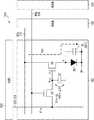
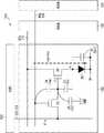
以下、図面を参照して、本発明の実施の形態を詳細に説明する。まず最初に、本発明の理解を容易にし且つ背景を明らかにするため、図1を参照して表示装置の一般的な構成を簡潔に説明する。図1は、一般的な表示装置の一画素分を示す模式的な回路図である。図示する様に、この画素回路にあっては、直交配列した走査線1Eと映像信号線1Fの交差部に、サンプリング用トランジスタ1Aが配置されている。このサンプリング用トランジスタ1AはN型であり、そのゲートが走査線1Eに接続されており、ドレインが映像信号線1Fに接続されている。このサンプリング用トランジスタ1Aのソースには保持容量1Cの一方の電極と、駆動用トランジスタ1Bのゲートとが接続されている。駆動用トランジスタ1BはN型で、そのドレインには電源供給線1Gが接続されており、そのソースには発光部1Dのアノードが接続されている。保持容量1Cの他方の電極と発光部1Dのカソードは、接地配線1Hに接続されている。Hereinafter, embodiments ofthe present invention will be described in detail with reference tothe drawings. First, in order to facilitate understanding ofthe present invention and to clarify the background, a general configuration of a display device will be briefly described with reference to FIG. FIG. 1 is a schematic circuit diagram showing one pixel of a general display device. As shown in the figure, in this pixel circuit, a
図2は、図1に示した画素回路の動作説明に供するタイミングチャートである。このタイミングチャートは、映像信号線(1F)から供給される映像信号の電位(映像信号線電位)をサンプリングし、有機ELデバイス等から成る発光部1Dを発光状態にする動作を表している。走査線(1E)の電位(走査線電位)が高レベルに遷移することで、サンプリング用トランジスタ(1A)はオン状態となり、映像信号線電位を保持容量(1C)に充電する。これにより、駆動用トランジスタ(1B)のゲート電位(Vg)は上昇を開始し、ドレイン電流を流し始める。その為、発光部(1D)のアノード電位は上昇し発光を開始する。この後、走査線電位が低レベルに遷移すると保持容量(1C)に映像信号線電位が保持され、駆動用トランジスタ(1B)のゲート電位が一定となり、発光輝度が次のフレームまで一定に維持される。FIG. 2 is a timing chart for explaining the operation of the pixel circuit shown in FIG. This timing chart samples the potential of the video signal supplied from thevideo signal line (1F) (video signal line potential), represents the operation of the
しかしながら、駆動用トランジスタ(1B)の製造プロセスのばらつきにより、各画素ごとに閾電圧や移動度等の特性変動がある。この特性変動により、駆動用トランジスタ(1B)に同一のゲート電位を与えても、画素毎にドレイン電流(駆動電流)が変動し、発光輝度のばらつきになって現れる。また、有機ELデバイス等から成る発光部(1D)の特性の経時変動により、発光部(1D)のアノード電位が変動する。アノード電位の変動は、駆動用トランジスタ(1B)のゲート−ソース間電圧の変動となって現れ、ドレイン電流(駆動電流)の変動を引き起こす。この様な種々の原因による駆動電流の変動は、画素ごとの発光輝度のばらつきとなって現れ、画質の劣化が起きる。However, due to variations in the manufacturing process ofthe driving transistor (1B), there are variations in characteristicssuch as threshold voltage and mobility for each pixel. Due to this characteristic variation, even if the same gate potential is applied to the driving transistor (1B), the drain current (driving current) varies from pixel to pixel, resulting in variations in light emission luminance. Further, the anode potential of thelight emitting unit (1D) varies due to the temporal variation of the characteristics of thelight emitting unit (1D)made of an organic EL deviceor the like . The fluctuation ofthe anode potential appears as a fluctuation of the gate- source voltage ofthe driving transistor (1B) and causes a fluctuation of the drain current (driving current). Such fluctuations inthe drive current due to various causes appear as variations in light emission luminance for each pixel, resulting in degradation of image quality.
図3Aは、本発明にかかる表示装置の全体構成を示すブロック図である。図示する様に、本表示装置100は、画素アレイ部102とこれを駆動する駆動部(103,104,105)とから成る。画素アレイ部102は、行状の走査線WSL101〜10mと、列状の映像信号線DTL101〜10nと、両者が交差する部分に配された行列状の画素(PXLC)101と、各画素(表示素子)101の各行に対応して配された電源供給線DSL101〜10mとを備えている。駆動部(103,104,105)は、各走査線WSL101〜10mに順次制御信号を供給して画素101を行単位で線順次走査する主スキャナ(ライトスキャナWSCN)104と、この線順次走査に合わせて各電源供給線DSL101〜10mに第1電位と第2電位とに切り換わる電源電圧を供給する電源スキャナ(DSCN)105と、この線順次走査に合わせて列状の映像信号線DTL101〜10nに映像信号となる信号電位と、基準電位とを供給する信号セレクタ(水平セレクタHSEL)103とを備えている。FIG. 3A is a block diagram showing the overall configuration of the display device according to the present invention. As shown, the
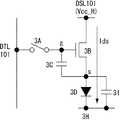
図3Bは、図3Aに示した表示装置100に含まれる画素101の具体的な構成及び結線関係を示す回路図である。図示する様に、この画素101は、有機ELデバイス等で代表される発光部3Dと、サンプリング用トランジスタ3Aと、駆動用トランジスタ3Bと、保持容量3Cとを含む。サンプリング用トランジスタ3Aは、そのゲートが対応する走査線WSL101に接続されており、そのソース及びドレインの一方が対応する映像信号線DTL101に接続されており、他方が駆動用トランジスタ3Bのゲートgに接続されている。駆動用トランジスタ3Bは、そのソースs及びドレインdの一方が発光部3Dに接続されており、他方が対応する電源供給線DSL101に接続されている。本実施形態では、駆動用トランジスタ3Bのドレインdが電源供給線DSL101に接続されている一方、ソースsが発光部3Dのアノードに接続されている。発光部3Dのカソードは接地配線3Hに接続されている。尚、この接地配線3Hは全ての画素101に対して共通に配線されている。保持容量3Cは、駆動用トランジスタ3Bのソースsとゲートgの間に接続されている。FIG. 3B is a circuit diagram showing a specific configuration and connection relationship of the
かかる構成において、サンプリング用トランジスタ3Aは、走査線WSL101から供給された制御信号に応じて導通し、映像信号線DTL101から供給された信号電位をサンプリングして保持容量3Cに保持する。駆動用トランジスタ3Bは、第1電位にある電源供給線DSL101から電流の供給を受け保持容量3Cに保持された信号電位に応じて駆動電流を発光部3Dに流す。主スキャナ(WSCN)104は、映像信号線DTL101が信号電位にある時間帯にサンプリング用トランジスタ3Aを導通状態にするため、この時間帯よりパルス幅の短い制御信号を走査線WSL101に出力し、以って、保持容量3Cに信号電位を保持する際、駆動用トランジスタ3Bの移動度μに対する補正を信号電位に加える。In this configuration, the
図3Bに示した画素回路101は、上述した移動度補正機能に加え閾電圧補正機能も備えている。即ち、電源スキャナ(DSCN)105は、サンプリング用トランジスタ3Aが信号電位をサンプリングする前に、第1タイミングで電源供給線DSL101を第1電位から第2電位に切り換える。また、主スキャナ(WSCN)104は、同じくサンプリング用トランジスタ3Aが信号電位をサンプリングする前に、第2タイミングでサンプリング用トランジスタ3Aを導通させて映像信号線DTL101から基準電位を駆動用トランジスタ3Bのゲートgに印加すると共に駆動用トランジスタ3Bのソースsを第2電位にセットする。通常、上述した第1タイミングは第2タイミングの前に来るが、場合によっては第1タイミングと第2タイミングを逆にしても良い。電源スキャナ(DSCN)105は、第2タイミングの後の第3タイミングで、電源供給線DSL101を第2電位から第1電位に切り換えて、駆動用トランジスタ3Bの閾電圧Vthに相当する電圧を保持容量3Cに保持しておく。かかる閾電圧補正機能により、本表示装置100は画素毎にばらつく駆動用トランジスタ3Bの閾電圧の影響をキャンセルすることが出来る。The
図3Bに示した画素回路101は、さらに、ブートストラップ機能も備えている。即ち、主スキャナ(WSCN)104は、保持容量3Cに信号電位が保持された段階で走査線WSL101に対する制御信号の印加を解除し、サンプリング用トランジスタ3Aを非導通状態にして駆動用トランジスタ3Bのゲートgを映像信号線DTL101から電気的に切り離し、以って、駆動用トランジスタ3Bのソース電位(Vs)の変動にゲート電位(Vg)が連動し、ゲートgとソースs間の電圧Vgsを一定に維持することが出来る。The
図4Aは、図3Bに示した画素101の動作説明に供するタイミングチャートである。時間軸を共通にして、走査線(WSL101)の電位変化、電源供給線(DSL101)の電位変化及び映像信号線(DTL101)の電位変化を表してある。また、これらの電位変化と並行に、駆動用トランジスタ3Bのゲート電位(Vg)及びソース電位(Vs)の変化も表してある。FIG. 4A is a timing chart for explaining the operation of the
このタイミングチャートは、画素101の動作の遷移に合わせて、期間を(B)〜(I)のように便宜的に区切ってある。発光期間(B)では、発光部3Dが発光状態にある。この後、線順次走査の新しいフィールドに入ってまず最初の期間(C)で、電源供給線を低電位に切り換える。次の期間(D)に進み、駆動用トランジスタのゲート電位Vg及びソース電位Vsを初期化する。この閾値補正準備期間(C)及び(D)で駆動用トランジスタ3Bのゲート電位Vg及びソース電位Vsをリセットすることで、閾電圧補正動作の準備が完了する。続いて、閾値補正期間(E)で実際に閾電圧補正動作が行われ、駆動用トランジスタ3Bのゲートgとソースsとの間に閾電圧Vthに相当する電圧が保持される。実際には、Vthに相当する電圧が、駆動用トランジスタ3Bのゲートgとソースsとの間に接続された保持容量3Cに書き込まれることになる。In this timing chart, the period is divided for convenience as (B) to (I) in accordance with the transition of the operation of the
この後、移動度補正の為の準備期間(F)及び(G)を経て、サンプリング期間/移動度補正期間(H)、即ち、第2期間に進む。ここで、映像信号の信号電位VinがVthに足し込まれる形で保持容量3Cに書き込まれると共に、移動度補正用の電圧ΔVが保持容量3Cに保持された電圧から差し引かれる。このサンプリング期間/移動度補正期間(H)では、映像信号線DTL101が信号電位Vinにある時間帯(第1期間内)にサンプリング用トランジスタ3Aを導通状態にするため、この時間帯よりパルス幅の短い第2期間の間、制御信号を走査線WSL101に出力し、以って、保持容量3Cに信号電位Vinを保持する際、駆動用トランジスタ3Bの移動度μに対する補正を信号電位Vinに加えている。Thereafter, after the preparation periods (F) and (G) for mobility correction, the process proceeds to the sampling period / mobility correction period (H), that is, the second period . Here, the signal potential Vin of the video signal along with written into the holding
この後、発光期間(I)に進み、信号電位Vinに応じた輝度で発光部が発光する。その際、信号電位Vinは閾電圧Vthに相当する電圧と移動度補正用の電圧ΔVとによって調整されているため、発光部3Dの発光輝度は駆動用トランジスタ3Bの閾電圧Vthや移動度μのばらつきの影響を受けることはない。尚、発光期間(I)の最初でブートストラップ動作が行われ、駆動用トランジスタ3Bのゲート−ソース間電圧Vgs=Vin−Vo+Vth−ΔVを一定に維持したまま、駆動用トランジスタ3Bのゲート電位Vg及びソース電位Vsが上昇する。Then, the process proceeds to the light emission period (I), the light emitting unit emits light with a luminance corresponding to the signal potential Vin. At that time, since the signal potential Vin that is adjusted by the voltage ΔV for the voltage and mobility correction corresponding to the threshold voltage Vth, the emission luminance of the
引き続き、図4B〜図4Iを参照して、図3Bに示した画素101の動作を詳細に説明する。尚、図4B〜図4Iの図番は、図4Aに示したタイミングチャートの各期間(B)〜(I)にそれぞれ対応している。理解を容易にするため、図4B〜図4Iにあっては、説明の都合上、発光部3Dの容量成分を容量素子3Iとして図示してある。先ず、図4Bに示すように発光期間(B)では、電源供給線DSL101が高電位Vcc_H(第1電位)にあり、駆動用トランジスタ3Bが駆動電流Idsを発光部3Dに供給している。図示する様に、駆動電流Idsは高電位Vcc_Hにある電源供給線DSL101から駆動用トランジスタ3Bを介して発光部3Dを通り、共通接地配線3Hに流れ込んでいる。Next, the operation of the
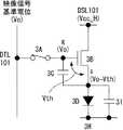
続いて、期間(C)に入ると図4Cに示すように、電源供給線DSL101を高電位Vcc_Hから低電位Vcc_Lに切り換える。これにより、電源供給線DSL101はVcc_Lまで放電され、さらに、駆動用トランジスタ3Bのソース電位VsはVcc_Lに近い電位まで遷移する。電源供給線DSL101の配線容量が大きい場合は、比較的早いタイミングで電源供給線DSL101を高電位Vcc_Hから低電位Vcc_Lに切り換えると良い。この期間(C)を十分に確保することで、配線容量やその他の画素寄生容量の影響を受けないようにしておく。Subsequently, as shown in FIG. 4C enters the period (C), changingturn off the power supply line DSL101 from the high potentialVcc - H to the low potentialVcc - L. As a result, the power supply line DSL101 is discharged toVcc_L , and the source potentialVs ofthe driving
次に、期間(D)に進むと図4Dに示すように、走査線WSL101を低レベルから高レベルに切り換えることで、サンプリング用トランジスタ3Aが導通状態になる。このとき、映像信号線DTL101は基準電位Voにある。よって、駆動用トランジスタ3Bのゲート電位Vgは、導通したサンプリング用トランジスタ3Aを通じて映像信号線DTL101の基準電位Voとなる。これと同時に、駆動用トランジスタ3Bのソース電位Vsは即座に低電位Vcc_Lに固定される。以上により、駆動用トランジスタ3Bのソース電位Vsが映像信号線DTLの基準電位Voより十分低い電位Vcc_Lに初期化(リセット)される。具体的には、駆動用トランジスタ3Bのゲート−ソース間電圧Vgs(ゲート電位Vgとソース電位Vsの差)が駆動用トランジスタ3Bの閾電圧Vthより大きくなるように、電源供給線DSL101の低電位Vcc_L(第2電位)を設定する。Next, as shown in FIG. 4D proceeds to period (D), the scanning line WSL101 Byperating the Came ra changes from low to high, the
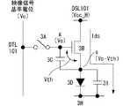
次に、閾値補正期間(E)に進むと、図4(E)に示すように、電源供給線DSL101の電位が低電位Vcc_Lから高電位Vcc_Hに遷移し、駆動用トランジスタ3Bのソース電位Vsが上昇を開始する。やがて、駆動用トランジスタ3Bのゲート−ソース間電圧Vgsが閾電圧Vthとなったところで、電流がカットオフする。このようにして、駆動用トランジスタ3Bの閾電圧Vthに相当する電圧が、保持容量3Cに書き込まれる。これが閾電圧補正動作である。このとき、電流が専ら保持容量3C側に流れ、発光部3D側には流れないようにするため、発光部3Dがカットオフとなるように共通接地配線3Hの電位を設定しておく。Then, the process proceeds to the threshold correction period(E), as shown in FIG. 4 (E),the potential of the power supply line DSL101 changes from the low potentialVcc - L to the high potentialVcc - H, the source potential of the driving
期間(F)に進むと、図4Fに示すように、走査線WSL101が低電位側に遷移し、サンプリング用トランジスタ3Aが一旦オフ状態になる。このとき、駆動用トランジスタ3Bのゲートgはフローティングになるが、ゲート−ソース間電圧Vgsは駆動用トランジスタ3Bの閾電圧Vthに等しいためカットオフ状態であり、ドレイン電流Idsは流れない。In the period (F), as shownin FIG. 4F, the scanning line WSL101 transits to the low potential side, and the
続いて、期間(G)に進むと、図4Gに示すように、映像信号線DTL101の電位が基準電位Voからサンプリング電位(信号電位)Vinに遷移する。これにより、次のサンプリング動作及び移動度補正動作の準備が完了する。Subsequently, the process proceeds to the period(G), as shown in FIG. 4G, the potential of the video signal line DTL101 is changed from the reference potentialVo to the sampling potential (signalpotential) Vin. This completes the preparation for the next sampling operation and mobility correction operation.
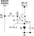
サンプリング期間/移動度補正期間(H)に入ると、図4Hに示すように、走査線WSL101が高電位側に遷移して、サンプリング用トランジスタ3Aがオン状態となる。したがって、駆動用トランジスタ3bのゲート電位Vgは信号電位Vinとなる。ここで、発光部3Dは始めカットオフ状態(ハイインピーダンス状態)にあるため、駆動用トランジスタ3Bのドレイン電流Idsは発光部の容量成分3Iに流れ込み、充電を開始する。したがって、駆動用トランジスタ3Bのソース電位Vsは上昇を開始し、やがて、駆動用トランジスタ3Bのゲート−ソース間電圧Vgsは、Vin−Vo+Vth−ΔVとなる。このようにして、信号電位Vinのサンプリングと補正量ΔVの調整が同時に行われる。Vinが高いほどIdsは大きくなり、ΔVの絶対値も大きくなる。したがって、発光輝度レベルに応じた移動度補正が行われる。Vinを一定とした場合、駆動用トランジスタ3Bの移動度μが大きいほどΔVの絶対値が大きくなる。換言すると、移動度μが大きいほど負帰還量ΔVが大きくなるので、画素ごとの移動度μのばらつきを取り除くことが出来る。In the sampling period / mobility correction period (H), as shown in FIG. 4H, the scanning line WSL101 transitions to the high potential side, and the
最後に、発光期間(I)になると、図4Iに示すように、走査線WSL101が低電位側に遷移し、サンプリング用トランジスタ3Aはオフ状態となる。これにより、駆動用トランジスタ3Bのゲートgは映像信号線DTL101から切り離される。同時にドレイン電流Idsが発光部3Dを流れ始める。これにより、発光部3Dのアノード電位は駆動電流Idsに応じて上昇する。上昇量をVelと表す。発光部3Dのアノード電位の上昇は、即ち、駆動用トランジスタ3Bのソース電位Vsの上昇に他ならない。駆動用トランジスタ3Bのソース電位Vsが上昇すると、保持容量3Cのブートストラップ動作により、駆動用トランジスタ3Bのゲート電位Vgも連動して上昇する。ゲート電位Vgの上昇量はソース電位Vsの上昇量に等しくなる。故に、発光期間中、駆動用トランジスタ3Bのゲート−ソース間電圧Vgsは、Vin−Vo+Vth−ΔVで一定に保持される。Finally, in the light emission period (I), as shown in FIG. 4I, the scanning line WSL101 transitions to the low potential side, and the
図5は、サンプリング期間/移動度補正期間(H)における、走査線電位波形及び映像信号線電位波形を示す模式図である。上側の波形は図3Aに示したライトスキャナ104から遠い側(遠側)で観測される波形を表しており、下側は逆にライトスキャナ104に近い側(近側)で観測される波形を表している。遠側では走査線電位(即ち、制御信号パルス)の波形が配線容量や配線抵抗の影響で大きく鈍り劣化している。これに対し近側では制御信号パルスは走査線の配線容量や配線抵抗の影響をあまり受けないため、波形は劣化していない。一方、映像信号線電位については、遠側および近側共に信号源である水平セレクタ103から同じ距離なので、波形に差が無い。FIG. 5 is a schematic diagram showing the scanning line potential waveform and the video signal line potential waveform in the sampling period / mobility correction period (H). The upper waveform represents a waveform observed on the side far from the light scanner 104 (far side) shown in FIG. 3A, and the lower side represents the waveform observed on the side closer to the light scanner 104 (near side). Represents. On the far side, the waveform of the scanning line potential (that is, the control signal pulse) is greatly dull and deteriorated due to the influence of wiring capacitance and wiring resistance. On the other hand, the control signal pulse is not greatly affected by the wiring capacitance and wiring resistance of the scanning line on the near side, and the waveform is not deteriorated. On the other hand, since the video signal line potential isthe same distance from the
ここで、移動度補正時間は、映像信号線電位が信号電位にある時間幅と制御信号パルスの両者が重なった範囲で決まる。特に本発明は映像信号線が信号電位にある時間幅の中に入るように制御信号パルス幅tを細めに決めているため、結果的に移動度補正時間t1は制御信号パルス幅tで決まる。正確には、制御信号パルスが立ち上がってサンプリング用トランジスタがオンしてから、同じく制御信号パルスが立下がってサンプリング用トランジスタがオフするまでの時間となる。図示する様に、オンタイミングはサンプリング用トランジスタ3Aのソース電位(即ち、映像信号線電位)に対して同じくサンプリング用トランジスタ3Aのゲート電位(即ち、走査線電位)がサンプリング用トランジスタの閾電圧Vth(3A)を超えた時となる。逆にサンプリング用トランジスタのオフタイミングは、そのゲート電位がソース電位に比べて丁度Vth(3A)を下回った時となる。よって移動度補正時間は図示する様に、波形が大きく鈍る遠側でt1になる一方、波形があまり鈍らない近側でt2となる。ここで波形が大きく鈍って劣化する遠側では、近側に比べてサンプリング用トランジスタのオンタイミングが後方にずれるが、オフタイミングも後方にシフトする。したがって、両者の差で決まる移動度補正時間t1は結局近側の移動度補正時間t2とあまり変わらないことになる。Here,the mobility correction time is determined by a range in which both the time width in which the video signal line potential is at the signal potential and the control signal pulse overlap. In particular, according to the present invention, the control signal pulse width t is determined to be narrow so that the video signal line falls within the time width at the signal potential. As a result, the mobility correction time t1 is determined by the control signal pulse width t. More precisely, it is the time from when the control signal pulse rises and the sampling transistor is turned on until the control signal pulse falls and the sampling transistor is turned off. As shown in the figure, the on-timing is the same as the source potential (ie, video signal line potential) of the
また、サンプリング用トランジスタ3Aによって最終的にサンプリングされる信号電位(サンプリング電位)は、丁度サンプリング用トランジスタ3Aがオフになった時の映像信号線電位で与えられる。図から明らかなように、近側及び遠側共にサンプリング電位V1,V2は信号電位Vinとなり差はない。この様に、本発明では遠側と近側でサンプリングされる映像信号線電位V1,V2はほとんど差は無い。さらに、移動度補正時間t1,t2についてもほとんど差は無視できる程度である。これにより、本発明にかかる表示装置は画面の左右で輝度差が現れることが無く、シェーディングは抑制され良好な画質の表示装置を得ることが出来る。Further, finally sampled the signal potential by the
図6は、同じくサンプリング期間/移動度補正期間(H)で観測される走査線電位波形及び映像信号線電位波形を示している。但し図面上半分は、水平セレクタ103から離れた画面下側で観測される波形を表しており、下半分は同じく水平セレクタ103に近い画面上側で観測される波形を表している。制御信号パルスの波形(走査線電位波形)は画面の上下で同じ位置を取っているため差は無い。一方、映像信号線電位は画面上側に比べて画面下側が配線容量や配線抵抗の影響で遅延している。しかしながら映像信号線に現れる信号電位波形が遅延しても、制御信号パルスが映像信号線が信号電位にある時間幅に入っている限り、サンプリング電位や移動度補正時間にほとんど差は無い。図から明らかなように、画面下側と上側で、サンプリングされる映像信号線電位V1,V2はほぼ等しい。また、移動度補正時間t1及びt2もほぼ等しくなる。これにより、画面の上側と下側との間の輝度差は抑制され、良好な画質の表示装置を得ることが出来る。FIG. 6 shows the scanning line potential waveform and the video signal line potential waveform that are also observed in the sampling period / mobility correction period (H). However, the upper half of the drawing represents the waveform observed on the lower side of the screen away from the
図7Aは図3Bに示した表示装置の駆動方法の参考例を表しており、理解を容易にするため図4Aのタイミングチャートと同じフォーマットを採用している。異なる点はサンプリング期間/移動度補正期間の制御方式である。図7Aに示すように、この参考例では、サンプリング期間/移動度補正期間(F)は、映像信号線が基準電位Voから信号電位Vinに立上がった時点から走査線が高電位から低電位に立下がる時点までとしている。FIG. 7A shows a reference example of the driving method of the display device shown in FIG. 3B, and adopts the same format as the timing chart of FIG. 4A for easy understanding. The difference is the control method of the sampling period / mobility correction period. As shown in FIG. 7A, in this reference example, the sampling period / mobility correction period (F) is scan line from the high potential at a point of time when the image signal line rises from the reference potentialVo to the signal potentialVin the low Until the time when the potential falls.
図7Aに示した参考例の動作方法を、さらに図7B〜図7Gを参照して説明する。先ず図7Bに示すように発光期間(B)では、電源供給線DSL101が高電位Vcc_H(第1電位)にあり、駆動用トランジスタ3Bが駆動電流Idsを発光部3Dに供給している。図示する様に、駆動電流Idsは高電位Vcc_Hにある電源供給線DSL101から駆動用トランジスタ3Bを介して発光部3Dを通り、共通接地配線3Hに流れ込んでいる。The operation method of the reference example shown in FIG. 7A will be further described with reference to FIGS. 7B to 7G. First, in the light emitting period (B), as shown in FIG. 7B, the power supply line DSL101 is at a high potentialVcc - H (first potential), the
続いて、期間(C)に入ると図7Cに示すように、電源供給線DSL101を高電位Vcc_Hから低電位Vcc_Lに切り換える。これにより、電源供給線DSL101はVcc_Lまで放電され、さらに、駆動用トランジスタ3Bのソース電位VsはVcc_Lに近い電位まで遷移する。電源供給線DSL101の配線容量が大きい場合は比較的早いタイミングで電源供給線DSL101を高電位Vcc_Hから低電位Vcc_Lに切り換えると良い。この期間(C)を十分に確保することで、配線容量やその他の画素寄生容量の影響を受けないようにしておく。Subsequently, as shown in FIG. 7C enters the period (C), changingturn off the power supply line DSL101 from the high potentialVcc - H to the low potentialVcc - L. As a result, the power supply line DSL101 is discharged toVcc_L , and the source potentialVs ofthe driving
次に、期間(D)に進むと図7Dに示すように、走査線WSL101を低レベルから高レベルに切り換えることで、サンプリング用トランジスタ3Aが導通状態になる。このとき映像信号線DTL101は基準電位Voにある。よって駆動用トランジスタ3Bのゲート電位Vgは導通したサンプリング用トランジスタ3Aを通じて映像信号線DTL101の基準電位Voとなる。これと同時に駆動用トランジスタ3Bのソース電位Vsは即座に低電位Vcc_Lに固定される。以上により駆動用トランジスタ3Bのソース電位Vsが映像信号線DTLの基準電位Voより十分低い電位Vcc_Lに初期化(リセット)される。具体的には、駆動用トランジスタ3Bのゲート−ソース間電圧Vgs(ゲート電位Vgとソース電位Vsの差)が駆動用トランジスタ3Bの閾電圧Vthより大きくなるように、電源供給線DSL101の低電位Vcc_L(第2電位)を設定する。Next, as shown in FIG. 7D proceeds to period (D), the scanning line WSL101 Byperating the Came ra changes from low to high, the
次に、閾値補正期間(E)に進むと図7(E)に示すように、電源供給線DSL101の電位が低電位Vcc_Lから高電位Vcc_Hに遷移し、駆動用トランジスタ3Bのソース電位Vsが上昇を開始する。やがて駆動用トランジスタ3Bのゲート−ソース間電圧Vgsが閾電圧Vthとなったところで電流がカットオフする。このようにして駆動用トランジスタ3Bの閾電圧Vthに相当する電圧が保持容量3Cに書き込まれる。これが閾電圧補正動作である。このとき電流が専ら保持容量3C側に流れ、発光部3D側には流れないようにするため、発光部3Dがカットオフとなるように共通接地配線3Hの電位を設定しておく。Next, as shown in FIG. 7 (E) Proceeding to the threshold correction period (E), the potential of the power supply line DSL101 changes from the low potentialVcc - L to the high potentialVcc - H, the source potentialV of the
次に、サンプリング期間/移動度補正期間(F)に進むと、図7Fに示すように、第1のタイミングで映像信号線DTL101の電位が基準電位Voから信号電位Vinに遷移し、駆動用トランジスタ3Bのゲート電位VgはVinとなる。このとき発光部3Dは始めカットオフ状態(ハイインピーダンス状態)にあるため駆動用トランジスタ3Bのドレイン電流Idsは発光部の容量成分3Iに流れ込む。これにより、発光部の容量成分3Iは充電を開始する。よって駆動用トランジスタ3Bのソース電位Vsは上昇を開始し、第2のタイミングで駆動用トランジスタ3Bのゲート−ソース間電圧Vgsは、Vin−Vo+Vth−ΔVとなる。このようにして信号電位Vinのサンプリングと補正量ΔVの調整が行われる。Vinが高いほどIdsは大きくなり、ΔVの絶対値も大きくなる。したがって、発光輝度レベルに応じた移動度補正が行える。また、Vinを一定とした場合、駆動用トランジスタ3Bの移動度μが大きいほどΔVの絶対値も大きくなる。換言すると、移動度μが大きいほど負帰還量ΔVが大きくなるので、画素ごとの移動度μのばらつきを取り除くことが可能である。Then, the process proceeds to the sampling period / mobility correction period (F), as shown in FIG. 7F, transits from the potential reference potential Vo of the video signal line DTL101 to the signal potential Vin at the first timing, the drive The gate potential Vg of the
最後に発光期間(G)になると、図7Gに示すように、走査線WSL101が低電位側に遷移し、サンプリング用トランジスタ3Aはオフ状態となる。これにより、駆動用トランジスタ3Bのゲートgは映像信号線DTL101から切り離される。同時にドレイン電流Idsが発光部3Dを流れ始める。これにより、発光部3Dのアノード電位は駆動電流Idsに応じて上昇する。上昇量をVelと表す。発光部3Dのアノード電位の上昇は、即ち、駆動用トランジスタ3Bのソース電位Vsの上昇に他ならない。駆動用トランジスタ3Bのソース電位Vsが上昇すると、保持容量3Cのブートストラップ動作により、駆動用トランジスタ3Bのゲート電位Vgも連動して上昇する。ゲート電位Vgの上昇量はソース電位Vsの上昇量Velに等しくなる。故に、発光期間中駆動用トランジスタ3Bのゲート−ソース間電圧VgsはVin−Vo+Vth−ΔVで一定に保持される。Finally, in the light emission period (G), as shown in FIG. 7G, the scanning line WSL101 transitions to the low potential side, and the
図8は、図7Aに示した参考例で、サンプリング期間/移動度補正期間(F)に観測される走査線電位波形及び映像信号線電位波形を表している。理解を容易にするため、図5に示した表記と同じフォーマットを採用している。図8の上側は画面のライトスキャナ104から遠く離れた側(遠側)で観測される波形を表しており、下側は画面のライトスキャナ104に近い側(近側)で観測される波形を表している。図示する様に、近側では配線抵抗と配線容量が小さいため走査線電位(制御信号パルス)は劣化しない。これに対し遠側は配線抵抗と配線容量が大きいため走査線電位(制御信号パルス)は大きく鈍って劣化する。一方、映像信号線電位は供給元の水平セレクタ103から等しい距離をとっているため、パルスの劣化の差は少ない。画面の近側と遠側で走査線電位の波形劣化が異なるため、近側と遠側でサンプリングされる映像信号線電位V1,V2に差が生じている。さらに移動度補正時間についても遠側と近側でt1とt2のように差が生じている。画面の遠側では走査線パルスの波形劣化が激しいため、サンプリング電位V1は大きくなり移動度補正時間t1も長くなる傾向になる。これに対し画面の近側では制御信号パルスの波形劣化がほとんどない為、サンプリング電位V2及び移動度補正時間t2共に設計値に近い値となる。この様に画面のライトスキャナに近い側と遠い側(即ち、画面の左右)でサンプリング電位や移動度補正時間が異なると画面の左右で輝度差が生じ、シェーディングとして視認される。FIG. 8 shows the scanning line potential waveform and the video signal line potential waveform observed in the sampling period / mobility correction period (F) in the reference example shown in FIG. 7A. In order to facilitate understanding, the same format as the notation shown in FIG. 5 is adopted. The upper side of FIG. 8 represents the waveform observed on the side far from the light scanner 104 (far side), and the lower side represents the waveform observed on the side near the light scanner 104 (near side). Represents. As shown in the figure, the scanning line potential (control signal pulse) does not deteriorate because the wiring resistance and wiring capacitance are small on the near side. On the other hand, since the wiring resistance and wiring capacitance are large on the far side, the scanning line potential (control signal pulse) is greatly dull and deteriorates. On the other hand, since the video signal line potential is at the same distance from the
最後に図9〜図11Cを参照して閾電圧補正動作、移動度補正動作及びブートストラップ動作につき更に説明する。図9は、駆動用トランジスタの電流電圧特性を示すグラフである。特に、駆動用トランジスタが飽和領域で動作しているときのドレイン−ソース間電流(ドレイン電流)Idsは、Ids=(1/2)・μ・(W/L)・Cox・(Vgs−Vth)2で表される。ここで、μは移動度を示し、Wはゲート幅を表し、Lはゲート長を表し、Coxは単位面積あたりのゲート酸化膜容量を示す。このトランジスタ特性式から明らかなように、閾電圧Vthが変動すると、Vgsが一定であっても、ドレイン−ソース間電流Idsが変動する。ここで、本発明にかかる画素は、前述したように発光時のゲート−ソース間電圧VgsがVin−Vo+Vth−ΔVで表されるため、これを上述のトランジスタ特性式に代入すると、ドレイン−ソース間電流Idsは、Ids=(1/2)・μ・(W/L)・Cox・(Vin−Vo−ΔV)2で表されることになり、閾電圧Vthに依存しない。結果として、閾電圧Vthが製造プロセスにより変動しても、ドレイン−ソース間電流Idsは変動せず、有機ELデバイスの発光輝度も変動しない。Finally, the threshold voltage correction operation, the mobility correction operation, and the bootstrap operation will be further described with reference to FIGS. 9 to 11C. FIG. 9 is a graph showing the current-voltage characteristics of the driving transistor. In particular, the drain-source current (drain current) Ids when the driving transistor operates in the saturation region is expressed as Ids = (1/2) · μ · (W / L) · Cox · (Vgs− Vth )2 Here, μ represents mobility, W represents gate width, L represents gate length, and Cox represents gate oxide film capacitance per unit area. As is clear from this transistor characteristic equation, when the threshold voltage Vth varies, the drain-source current Ids varies even if Vgs is constant. Here, in the pixel according to the present invention, as described above, the gate-source voltage Vgs during light emission is represented by Vin−Vo + Vth −ΔV. The drain-source current Ids is expressed as Ids = (1/2) · μ · (W / L) · Cox · (Vin−Vo −ΔV)2 It does not depend onVth . As a result, even if the threshold voltage Vth varies depending on the manufacturing process, the drain-source current Ids does not vary, and the light emission luminance of the organic EL device does not vary.
何ら対策を施さないと、図9に示すように閾電圧がVthのときVgsに対応する駆動電流がIdsとなるのに対し、閾電圧Vth’のとき同じゲート電圧Vgsに対応する駆動電流Ids’はIdsと異なってしまう。If no measures are taken, the drive current corresponding toVgs becomesIds when the threshold voltage isVth as shown in FIG. 9, whereas the same gate voltageVgs corresponds to the threshold voltageVth′. Drive currentIds′ to be different fromIds .
図10Aは同じく駆動用トランジスタの電流電圧特性を示すグラフである。移動度がμとμ’で異なる2個の駆動用トランジスタについて、それぞれ特性カーブを挙げてある。グラフから明らかなように、移動度がμとμ’で異なると、一定のVgsであってもドレイン−ソース間電流がIdsとIds’のようになり、変動してしまう。FIG. 10A is a graph showing the current-voltage characteristics of the driving transistor. Characteristic curves are given for two drive transistors having different mobility in μ and μ′ . As is apparent from the graph, when the mobility is different between μ and μ′ , the drain- source current becomesIds andIds′ and fluctuates even at a constantVgs .
図10Bは、映像信号線電位のサンプリング時及び移動度補正時における画素の動作を説明するもので、理解を容易にするため、発光部3Dの容量成分3Iも表してある。映像信号線電位のサンプリング時、サンプリング用トランジスタ3Aはオン状態であるため、駆動用トランジスタ3Bのゲート電位Vgは映像信号線電位Vinとなり、駆動用トランジスタ3Bのゲート−ソース間電圧VgsはVin−Vo+Vthになる。このとき、駆動用トランジスタ3Bはオン状態となり、さらに、発光部3Dはカットオフ状態であるため、ドレイン−ソース間電流Idsが発光部の容量成分3Iに流れ込む。ドレイン−ソース間電流Idsが発光部の容量成分3Iに流れ込むと、発光部の容量成分3Iは充電を開始し、発光部3Dのアノード電位(したがって、駆動用トランジスタ3Bのソース電位Vs)が上昇を開始する。駆動用トランジスタ3Bのソース電位VsがΔVだけ上昇すると、駆動用トランジスタ3Bのゲート−ソース間電圧VgsはΔVだけ減少する。これが負帰還による移動度補正動作であり、ゲート−ソース間電圧Vgsの減少量ΔVは、ΔV=Ids・t/Celで決定され、ΔVが移動度補正のためのパラメータとなる。ここで、Celは発光部の容量成分3Iの容量値を示し、tは移動度補正期間を示す。FIG. 10B illustrates the operation of the pixel when sampling the video signal line potential and correcting the mobility, and for the sake of easy understanding, the capacitive component 3I of the
図10Cは、移動度補正時における駆動用トランジスタ3Bの動作点を説明するグラフである。製造プロセスにおける移動度μ,μ’のばらつきに対して、上述した移動度補正をかけることによって最適の補正パラメータΔV及びΔV’が決定され、駆動用トランジスタ3Bのドレイン−ソース間電流Ids及びIds’が決定される。仮に移動度補正をかけないと、ゲート−ソース間電圧Vgsに対して、移動度がμとμ’で異なると、これに応じてドレイン−ソース間電流もIds0とIds0’で違ってしまう。これに対処するため移動度μ及びμ’に対してそれぞれ適切な補正ΔV及びΔV’をかけることで、ドレイン−ソース間電流がIds及びIds’となり、同レベルとなる。図10Cのグラフから明らかなように、移動度μが高いとき補正量ΔVが大きくなる一方、移動度μ’が小さいとき補正量ΔV’も小さくなるように、負帰還をかけている。FIG. 10C is a graph for explaining an operating point of the driving
図11Aは、有機ELデバイスで構成される発光部3Dの電流−電圧特性を示すグラフである。発光部3Dに電流Ielが流れるとき、アノード−カソード間電圧Velは一意的に決定される。図4Iに示したように発光期間中、走査線WSL101が低電位側に遷移し、サンプリング用トランジスタ3Aがオフ状態になると、発光部3Dのアノードは駆動用トランジスタ3Bのドレイン−ソース間電流Idsで決定されるアノード−カソード間電圧Vel分だけ上昇する。FIG. 11A is a graph showing the current- voltage characteristics of the
図11Bは、発光部3Dのアノード電位上昇時における駆動用トランジスタ3Bのゲート電位Vgとソース電位Vsの電位変動を示すグラフである。発光部3Dのアノード上昇電圧がVelのとき、駆動用トランジスタ3BのソースもVelだけ上昇し、保持容量3Cのブートストラップ動作により駆動用トランジスタ3BのゲートもVel分上昇する。この為、ブートストラップ前に保持された駆動用トランジスタ3Bのゲート−ソース間電圧Vgs=Vin−Vo+Vth−ΔVは、ブートストラップ後もそのまま保持される。また、発光部3Dの経時劣化によりそのアノード電位が変動しても、駆動用トランジスタ3Bのゲート−ソース間電圧は常にVin−Vo+Vth−ΔVで一定に保持される。FIG. 11B is a graph showing potential fluctuations of the gate potential Vg and the source potential Vs of the driving
図11Cは、図10Bで説明した本発明の画素構成に、寄生容量7A及び7Bを付加した回路図である。この寄生容量7A及び7Bは駆動用トランジスタ3のゲートgに寄生している。前述したブートストラップ動作能力は保持容量の容量値をCs、寄生容量7A,7Bの容量値をそれぞれCw,Cpとした場合に、Cs/(Cs+Cw+Cp)で表され、これが1に近いほどブートストラップ動作能力が高い。つまり発光部3Dの経時劣化に対する補正能力が高いことを示している。本発明では駆動用トランジスタ3Bのゲートgに接続する素子数を最小限にとどめており、Cpをほとんど無視できる。したがって、ブートストラップ動作能力はCs/(Cs+Cw)で表され、限りなく1に近いことになり、発光部3Dの経時劣化に対する補正能力が高いことを示している。FIG. 11C is a circuit diagram in which
図12は、本発明にかかる表示装置の他の実施形態を示す模式的な回路図である。理解を容易にするため、図3Bに示した先の実施形態と対応する部分には対応する参照番号を付してある。異なる点は、図3Bに示した実施形態がNチャネル型のトランジスタを用いて画素回路を構成しているのに対し、図12の実施形態はPチャネル型のトランジスタを用いて画素回路を構成していることである。図12の画素回路も、図3Bに示した画素回路とまったく同様に閾電圧補正動作、移動度補正動作及びブートストラップ動作を行うことが出来る。 FIG. 12 is a schematic circuit diagram showing another embodiment of the display device according to the present invention. For ease of understanding, parts corresponding to those of the previous embodiment shown in FIG. 3B are given corresponding reference numerals. The difference is that the embodiment shown in FIG. 3B uses an N-channel transistor to form a pixel circuit, whereas the embodiment shown in FIG. 12 uses a P-channel transistor to form a pixel circuit. It is that. The pixel circuit of FIG. 12 can perform the threshold voltage correction operation, the mobility correction operation, and the bootstrap operation in exactly the same manner as the pixel circuit shown in FIG. 3B.
100…表示装置、101…画素(表示素子)、102…画素アレイ部、103…水平セレクタ、104…ライトスキャナ、105…電源スキャナ、3A…サンプリング用トランジスタ、3B…駆動用トランジスタ、3C…保持容量、3D…発光部DESCRIPTION OF
Claims (4)
Translated fromJapanese画素アレイ部は、行状に配された複数の走査線、列状に配された複数の映像信号線、及び、行列状に配された表示素子、並びに、表示素子の各行に対応して配された電源線を備えており、
駆動部は、各走査線に順次制御信号を供給して表示素子を行単位で線順次走査する主スキャナと、線順次走査に合わせて各電源線に第1電位と第2電位で切り換わる電源電圧を供給する電源スキャナと、線順次走査に合わせて映像信号線に映像信号となる信号電位と基準電位を供給する信号セレクタとを備えており、
表示素子は、発光部と、サンプリング用トランジスタと、駆動用トランジスタと、保持容量とを含み、
サンプリング用トランジスタと駆動用トランジスタとは、それぞれ、ゲートと、ソース及びドレインの一方と、ソース及びドレインの他方とを備えており、
サンプリング用トランジスタにあっては、ゲートは走査線に接続されており、ソース及びドレインの一方は映像信号線に接続されており、
駆動用トランジスタにあっては、ゲートはサンプリング用トランジスタのソース及びドレインの他方と保持容量の一端とに接続されており、ソース及びドレインの一方は発光部の一端と保持容量の他端とに接続されており、ソース及びドレインの他方は電源線に接続されている表示装置の駆動方法であって、
駆動部の動作に基づいて、駆動用トランジスタのソース及びドレインの他方に供給される電源電圧を第1電位とした状態で、映像信号線の電位が信号電位にある第1期間内に、第1期間よりも短い第2期間の間、制御信号を走査線に供給してサンプリング用トランジスタを導通状態とし、以て、映像信号線から信号電位を駆動用トランジスタのゲートに印加する工程を備えており、
前記工程の前に、
駆動部の動作に基づいて、電源電圧を、第1電位から、基準電位からの差が駆動用トランジスタの閾電圧を超える第2電位に切り換え、次いで、映像信号線の電位が基準電位にある期間内に、走査線に別の制御信号を供給してサンプリング用トランジスタを導通状態として基準電位を駆動用トランジスタのゲートに印加し、以て、駆動用トランジスタのゲート電位とソース及びドレインの一方の電位とを初期化し、その後、電源電圧を第2電位から第1電位に切り換えることによって、駆動用トランジスタのソース及びドレインの一方の電位を基準電位から駆動用トランジスタの閾電圧を減じた電位に向かって近づけ、次いで、走査線への別の制御信号の供給を停止する工程、
を行い、
第2期間の終了と共に走査線への制御信号の供給が停止され、サンプリング用トランジスタが導通状態から非導通状態となることによって、駆動用トランジスタのゲート−ソース間電圧の値に応じたドレイン電流を発光部に流し、
第2期間において駆動用トランジスタのソース及びドレインの一方の電位が変化することによって、駆動用トランジスタのゲート−ソース間電圧の値が補正される、
表示装置の駆動方法。It consists of a pixel array part and a drive part that drives it,
The pixel array unit is arranged corresponding to a plurality of scanning lines arranged in rows, a plurality of video signal lines arranged in columns, display elements arranged in a matrix, and each row of the display elements. Power supply line,
The driving unit supplies a control signal to each scanning line sequentially to scan the display elements line by line, and a power source that switches each power line between the first potential and the second potential in accordance with the line sequential scanning. A power supply scanner that supplies a voltage, and a signal selector that supplies a signal potential and a reference potential to be a video signal to the video signal line in accordance with line sequential scanning,
The display element includes a light emitting unit, a sampling transistor, a driving transistor, and a storage capacitor.
Each of the sampling transistor and the driving transistor includes a gate, one of a source and a drain, and the other of the source and the drain,
In the sampling transistor, the gate is connected to the scanning line, and one of the source and the drain is connected to the video signal line,
In the driving transistor, the gate is connected to the other of the source and drain of the sampling transistor and one end of the storage capacitor, and one of the source and drain is connected to one end of the light emitting unit and the other end of the storage capacitor. And the other of the source and the drain is a method for driving a display device connected to a power line,
Based on the operation of the driving unit, the first voltage is supplied to the other of the source and the drain of the driving transistor, and the first potential is within the first period in which the potential of the video signal line is at the signal potential. For a second period shorter than the period, a step of supplying a control signal to the scanning line to turn on the sampling transistor and applying a signal potential from the video signal line to the gate of the driving transistor is provided. ,
Before the process,
Based on the operation of the driving unit, the power supply voltage is switched from the first potential to the second potential where the difference from the reference potential exceeds the threshold voltage of the driving transistor, and then the period in which the potential of the video signal line is at the reference potential In addition, another control signal is supplied to the scanning line to make the sampling transistor conductive, and a reference potential is applied to the gate of the driving transistor, so that the gate potential of the driving transistor and one of the source and drain potentials are applied. Then, the power supply voltage is switched from the second potential to the first potential, so that one of the source and drain potentials of the driving transistor is changed to a potential obtained by subtracting the threshold voltage of the driving transistor from the reference potential. Approaching and then stopping the supply of another control signal to the scan line;
Thestomach line,
With the end of the second period, the supply of the control signal to the scanning line is stopped, and the sampling transistor is changed from the conductive state to the non-conductive state, whereby the drain current corresponding to the gate-source voltage value of the driving transistor is set. Pour into the light emitting part,
The value of the gate-source voltage of the driving transistor is corrected by changing the potential of one of the source and the drain of the driving transistor in the second period.
A driving method of a display device.
画素アレイ部は、行状に配された複数の走査線、列状に配された複数の映像信号線、及び、行列状に配された表示素子、並びに、表示素子の各行に対応して配された電源線を備えており、
駆動部は、各走査線に順次制御信号を供給して表示素子を行単位で線順次走査する主スキャナと、線順次走査に合わせて各電源線に第1電位と第2電位で切り換わる電源電圧を供給する電源スキャナと、線順次走査に合わせて映像信号線に映像信号となる信号電位と基準電位を供給する信号セレクタとを備えており、
表示素子は、発光部と、サンプリング用トランジスタと、駆動用トランジスタと、保持容量とを含み、
サンプリング用トランジスタと駆動用トランジスタとは、それぞれ、ゲートと、ソース及びドレインの一方と、ソース及びドレインの他方とを備えており、
サンプリング用トランジスタにあっては、ゲートは走査線に接続されており、ソース及びドレインの一方は映像信号線に接続されており、
駆動用トランジスタにあっては、ゲートはサンプリング用トランジスタのソース及びドレインの他方と保持容量の一端とに接続されており、ソース及びドレインの一方は発光部の一端と保持容量の他端とに接続されており、ソース及びドレインの他方は電源線に接続されている表示装置の駆動方法であって、
駆動部の動作に基づいて、駆動用トランジスタのソース及びドレインの他方に供給される電源電圧を第1電位とした状態で、映像信号線の電位が信号電位にある第1期間内に、第1期間よりも短い第2期間の間、制御信号を走査線に供給してサンプリング用トランジスタを導通状態とし、以て、映像信号線から信号電位を駆動用トランジスタのゲートに印加する工程を備えており、
前記工程の前に、
駆動部の動作に基づいて、映像信号線の電位が基準電位にある期間内に、走査線に別の制御信号を供給してサンプリング用トランジスタを導通状態として基準電位を駆動用トランジスタのゲートに印加し、次いで、電源電圧を、第1電位から、基準電位からの差が駆動用トランジスタの閾電圧を超える第2電位に切り換え、以て、駆動用トランジスタのゲート電位とソース及びドレインの一方の電位とを初期化し、その後、電源電圧を第2電位から第1電位に切り換えることによって、駆動用トランジスタのソース及びドレインの一方の電位を基準電位から駆動用トランジスタの閾電圧を減じた電位に向かって近づけ、次いで、走査線への別の制御信号の供給を停止する工程、
を行い、
第2期間の終了と共に走査線への制御信号の供給が停止され、サンプリング用トランジスタが導通状態から非導通状態となることによって、駆動用トランジスタのゲート−ソース間電圧の値に応じたドレイン電流を発光部に流し、
第2期間において駆動用トランジスタのソース及びドレインの一方の電位が変化することによって、駆動用トランジスタのゲート−ソース間電圧の値が補正される、
表示装置の駆動方法。It consists of a pixel array part and a drive part that drives it,
The pixel array unit is arranged corresponding to a plurality of scanning lines arranged in rows, a plurality of video signal lines arranged in columns, display elements arranged in a matrix, and each row of the display elements. Power supply line,
The driving unit supplies a control signal to each scanning line sequentially to scan the display elements line by line, and a power source that switches each power line between the first potential and the second potential in accordance with the line sequential scanning. A power supply scanner that supplies a voltage, and a signal selector that supplies a signal potential and a reference potential to be a video signal to the video signal line in accordance with line sequential scanning,
The display element includes a light emitting unit, a sampling transistor, a driving transistor, and a storage capacitor.
Each of the sampling transistor and the driving transistor includes a gate, one of a source and a drain, and the other of the source and the drain,
In the sampling transistor, the gate is connected to the scanning line, and one of the source and the drain is connected to the video signal line,
In the driving transistor, the gate is connected to the other of the source and drain of the sampling transistor and one end of the storage capacitor, and one of the source and drain is connected to one end of the light emitting unit and the other end of the storage capacitor. And the other of the source and the drain is a method for driving a display device connected to a power line,
Based on the operation of the driving unit, the first voltage is supplied to the other of the source and the drain of the driving transistor, and the first potential is within the first period in which the potential of the video signal line is at the signal potential. For a second period shorter than the period, a step of supplying a control signal to the scanning line to turn on the sampling transistor and applying a signal potential from the video signal line to the gate of the driving transistor is provided. ,
Before the process,
Based on the operation of the drive unit, within the period when the potential of the video signal line is at the reference potential, another control signal is supplied to the scanning line to turn on the sampling transistor and apply the reference potential to the gate of the drive transistor. Then, the power supply voltage is switched from the first potential to the second potential where the difference from the reference potential exceeds the threshold voltage of the driving transistor, so that the gate potential of the driving transistor and one of the source and drain potentials Then, the power supply voltage is switched from the second potential to the first potential, so that one of the source and drain potentials of the driving transistor is changed to a potential obtained by subtracting the threshold voltage of the driving transistor from the reference potential. Approaching and then stopping the supply of another control signal to the scan line;
Thestomach line,
With the end of the second period, the supply of the control signal to the scanning line is stopped, and the sampling transistor is changed from the conductive state to the non-conductive state, whereby the drain current corresponding to the gate-source voltage value of the driving transistor is set. Pour into the light emitting part,
The value of the gate-source voltage of the driving transistor is corrected by changing the potential of one of the source and the drain of the driving transistor in the second period.
A driving method of a display device.
行状に配された走査線と列状に配された映像信号線とが交差する部分に配され、
発光部と、サンプリング用トランジスタと、駆動用トランジスタと、保持容量とを含み、
サンプリング用トランジスタと駆動用トランジスタとは、それぞれ、ゲートと、ソース及びドレインの一方と、ソース及びドレインの他方とを備えており、
サンプリング用トランジスタにあっては、ゲートは走査線に接続されており、ソース及びドレインの一方は映像信号線に接続されており、
駆動用トランジスタにあっては、ゲートはサンプリング用トランジスタのソース及びドレインの他方と保持容量の一端とに接続されており、ソース及びドレインの一方は発光部の一端と保持容量の他端とに接続されており、ソース及びドレインの他方は電源線に接続されている表示素子、
を用いた表示素子の駆動方法であって、
駆動部の動作に基づいて、駆動用トランジスタのソース及びドレインの他方に供給される電源電圧を第1電位とした状態で、サンプリング用トランジスタのソース及びドレインの一方の電位が信号電位にある第1期間内に、第1期間よりも短い第2期間の間、制御信号をサンプリング用トランジスタのゲートに供給してサンプリング用トランジスタを導通状態とし、以て、信号電位を駆動用トランジスタのゲートに印加する工程を備えており、
前記工程の前に、
駆動部の動作に基づいて、電源電圧を、第1電位から、基準電位からの差が駆動用トランジスタの閾電圧を超える第2電位に切り換え、次いで、映像信号線の電位が基準電位にある期間内に、走査線に別の制御信号を供給してサンプリング用トランジスタを導通状態として基準電位を駆動用トランジスタのゲートに印加し、以て、駆動用トランジスタのゲート電位とソース及びドレインの一方の電位とを初期化し、その後、電源電圧を第2電位から第1電位に切り換えることによって、駆動用トランジスタのソース及びドレインの一方の電位を基準電位から駆動用トランジスタの閾電圧を減じた電位に向かって近づけ、次いで、走査線への別の制御信号の供給を停止する工程、
を行い、
第2期間の終了と共にサンプリング用トランジスタのゲートへの制御信号の供給が停止され、サンプリング用トランジスタが導通状態から非導通状態となることによって、駆動用トランジスタのゲート−ソース間電圧の値に応じたドレイン電流を発光部に流し、
第2期間において駆動用トランジスタのソース及びドレインの一方の電位が変化することによって、駆動用トランジスタのゲート−ソース間電圧の値が補正される、
表示素子の駆動方法。A main scanner that sequentially supplies control signals to the scanning lines, a power supply scanner that supplies power supply voltages that switch between the first potential and the second potential, and a signal potential that becomes a video signal and a reference potential are supplied to the video signal lines. A drive unit including a signal selector, and
It is arranged at the intersection of the scanning lines arranged in rows and the video signal lines arranged in columns,
Including a light emitting unit, a sampling transistor, a driving transistor, and a storage capacitor;
Each of the sampling transistor and the driving transistor includes a gate, one of a source and a drain, and the other of the source and the drain,
In the sampling transistor, the gate is connected to the scanning line, and one of the source and the drain is connected to the video signal line,
In the driving transistor, the gate is connected to the other of the source and drain of the sampling transistor and one end of the storage capacitor, and one of the source and drain is connected to one end of the light emitting unit and the other end of the storage capacitor. The other of the source and the drain is connected to the power supply line,
A display element driving method using
Based on the operation of the driving unit, a first potential in which one of the source and drain of the sampling transistor is at the signal potential in a state where the power supply voltage supplied to the other of the source and drain of the driving transistor is set to the first potential. Within the period, during a second period shorter than the first period, a control signal is supplied to the gate of the sampling transistor to turn on the sampling transistor, and thus a signal potential is applied to the gate of the driving transistor. It has a process,
Before the process,
Based on the operation of the driving unit, the power supply voltage is switched from the first potential to the second potential where the difference from the reference potential exceeds the threshold voltage of the driving transistor, and then the period in which the potential of the video signal line is at the reference potential In addition, another control signal is supplied to the scanning line to make the sampling transistor conductive, and a reference potential is applied to the gate of the driving transistor, so that the gate potential of the driving transistor and one of the source and drain potentials are applied. Then, the power supply voltage is switched from the second potential to the first potential, so that one of the source and drain potentials of the driving transistor is changed to a potential obtained by subtracting the threshold voltage of the driving transistor from the reference potential. Approaching and then stopping the supply of another control signal to the scan line;
Thestomach line,
With the end of the second period, the supply of the control signal to the gate of the sampling transistor is stopped, and the sampling transistor is changed from the conducting state to the non-conducting state, so that the value of the voltage between the gate and the source of the driving transistor is met. A drain current is passed through the light emitting part,
The value of the gate-source voltage of the driving transistor is corrected by changing the potential of one of the source and the drain of the driving transistor in the second period.
A display element driving method.
行状に配された走査線と列状に配された映像信号線とが交差する部分に配され、
発光部と、サンプリング用トランジスタと、駆動用トランジスタと、保持容量とを含み、
サンプリング用トランジスタと駆動用トランジスタとは、それぞれ、ゲートと、ソース及びドレインの一方と、ソース及びドレインの他方とを備えており、
サンプリング用トランジスタにあっては、ゲートは走査線に接続されており、ソース及びドレインの一方は映像信号線に接続されており、
駆動用トランジスタにあっては、ゲートはサンプリング用トランジスタのソース及びドレインの他方と保持容量の一端とに接続されており、ソース及びドレインの一方は発光部の一端と保持容量の他端とに接続されており、ソース及びドレインの他方は電源線に接続されている表示素子、
を用いた表示素子の駆動方法であって、
駆動部の動作に基づいて、駆動用トランジスタのソース及びドレインの他方に供給される電源電圧を第1電位とした状態で、サンプリング用トランジスタのソース及びドレインの一方の電位が信号電位にある第1期間内に、第1期間よりも短い第2期間の間、制御信号をサンプリング用トランジスタのゲートに供給してサンプリング用トランジスタを導通状態とし、以て、信号電位を駆動用トランジスタのゲートに印加する工程を備えており、
前記工程の前に、
駆動部の動作に基づいて、映像信号線の電位が基準電位にある期間内に、走査線に別の制御信号を供給してサンプリング用トランジスタを導通状態として基準電位を駆動用トランジスタのゲートに印加し、次いで、電源電圧を、第1電位から、基準電位からの差が駆動用トランジスタの閾電圧を超える第2電位に切り換え、以て、駆動用トランジスタのゲート電位とソース及びドレインの一方の電位とを初期化し、その後、電源電圧を第2電位から第1電位に切り換えることによって、駆動用トランジスタのソース及びドレインの一方の電位を基準電位から駆動用トランジスタの閾電圧を減じた電位に向かって近づけ、次いで、走査線への別の制御信号の供給を停止する工程、
を行い、
第2期間の終了と共にサンプリング用トランジスタのゲートへの制御信号の供給が停止され、サンプリング用トランジスタが導通状態から非導通状態となることによって、駆動用トランジスタのゲート−ソース間電圧の値に応じたドレイン電流を発光部に流し、
第2期間において駆動用トランジスタのソース及びドレインの一方の電位が変化することによって、駆動用トランジスタのゲート−ソース間電圧の値が補正される、
表示素子の駆動方法。A main scanner that sequentially supplies control signals to the scanning lines, a power supply scanner that supplies power supply voltages that switch between the first potential and the second potential, and a signal potential that becomes a video signal and a reference potential are supplied to the video signal lines. A drive unit including a signal selector, and
It is arranged at the intersection of the scanning lines arranged in rows and the video signal lines arranged in columns,
Including a light emitting unit, a sampling transistor, a driving transistor, and a storage capacitor;
Each of the sampling transistor and the driving transistor includes a gate, one of a source and a drain, and the other of the source and the drain,
In the sampling transistor, the gate is connected to the scanning line, and one of the source and the drain is connected to the video signal line,
In the driving transistor, the gate is connected to the other of the source and drain of the sampling transistor and one end of the storage capacitor, and one of the source and drain is connected to one end of the light emitting unit and the other end of the storage capacitor. The other of the source and the drain is connected to the power supply line,
A display element driving method using
Based on the operation of the driving unit, a first potential in which one of the source and drain of the sampling transistor is at the signal potential in a state where the power supply voltage supplied to the other of the source and drain of the driving transistor is set to the first potential. Within the period, during a second period shorter than the first period, a control signal is supplied to the gate of the sampling transistor to turn on the sampling transistor, and thus a signal potential is applied to the gate of the driving transistor. It has a process,
Before the process,
Based on the operation of the drive unit, within the period when the potential of the video signal line is at the reference potential, another control signal is supplied to the scanning line to turn on the sampling transistor and apply the reference potential to the gate of the drive transistor. Then, the power supply voltage is switched from the first potential to the second potential where the difference from the reference potential exceeds the threshold voltage of the driving transistor, so that the gate potential of the driving transistor and one of the source and drain potentials Then, the power supply voltage is switched from the second potential to the first potential, so that one of the source and drain potentials of the driving transistor is changed to a potential obtained by subtracting the threshold voltage of the driving transistor from the reference potential. Approaching and then stopping the supply of another control signal to the scan line;
Thestomach line,
With the end of the second period, the supply of the control signal to the gate of the sampling transistor is stopped, and the sampling transistor is changed from the conductive state to the non-conductive state, so that the value of the voltage between the gate and the source of the driving transistor is met. A drain current is passed through the light emitting part,
The value of the gate-source voltage of the driving transistor is corrected by changing the potential of one of the source and the drain of the driving transistor in the second period.
A display element driving method.
Priority Applications (6)
| Application Number | Priority Date | Filing Date | Title |
|---|---|---|---|
| JP2006204057AJP4984715B2 (en) | 2006-07-27 | 2006-07-27 | Display device driving method and display element driving method |
| US11/826,875US8390543B2 (en) | 2006-07-27 | 2007-07-19 | Display device, driving method thereof, and electronic apparatus |
| TW096126374ATWI377544B (en) | 2006-07-27 | 2007-07-19 | Display device, driving method thereof, and electronic apparatus |
| KR1020070073957AKR101402815B1 (en) | 2006-07-27 | 2007-07-24 | Display device, driving method thereof, and electronic apparatus |
| CN2007101821848ACN101140732B (en) | 2006-07-27 | 2007-07-27 | Display device, driving method thereof, and electronic device |
| US13/743,629US9099041B2 (en) | 2006-07-27 | 2013-01-17 | Display device with a correction period of a threshold voltage of a driver transistor and electronic apparatus |
Applications Claiming Priority (1)
| Application Number | Priority Date | Filing Date | Title |
|---|---|---|---|
| JP2006204057AJP4984715B2 (en) | 2006-07-27 | 2006-07-27 | Display device driving method and display element driving method |
Publications (3)
| Publication Number | Publication Date |
|---|---|
| JP2008032863A JP2008032863A (en) | 2008-02-14 |
| JP2008032863A5 JP2008032863A5 (en) | 2009-10-01 |
| JP4984715B2true JP4984715B2 (en) | 2012-07-25 |
Family
ID=39122377
Family Applications (1)
| Application Number | Title | Priority Date | Filing Date |
|---|---|---|---|
| JP2006204057AActiveJP4984715B2 (en) | 2006-07-27 | 2006-07-27 | Display device driving method and display element driving method |
Country Status (5)
| Country | Link |
|---|---|
| US (2) | US8390543B2 (en) |
| JP (1) | JP4984715B2 (en) |
| KR (1) | KR101402815B1 (en) |
| CN (1) | CN101140732B (en) |
| TW (1) | TWI377544B (en) |
Families Citing this family (29)
| Publication number | Priority date | Publication date | Assignee | Title |
|---|---|---|---|---|
| JP5114889B2 (en)* | 2006-07-27 | 2013-01-09 | ソニー株式会社 | Display element, display element drive method, display device, and display device drive method |
| JP2008158378A (en)* | 2006-12-26 | 2008-07-10 | Sony Corp | Display device and method of driving the same |
| JP5023906B2 (en)* | 2007-09-12 | 2012-09-12 | ソニー株式会社 | Display device and driving method of display device |
| JP5186950B2 (en)* | 2008-02-28 | 2013-04-24 | ソニー株式会社 | EL display panel, electronic device, and driving method of EL display panel |
| JP2009204992A (en)* | 2008-02-28 | 2009-09-10 | Sony Corp | El display panel, electronic device, and drive method of el display panel |
| JP5125671B2 (en)* | 2008-03-26 | 2013-01-23 | ソニー株式会社 | Image display device, defect detection method, and short-circuit accident repair method |
| JP4640443B2 (en) | 2008-05-08 | 2011-03-02 | ソニー株式会社 | Display device, display device driving method, and electronic apparatus |
| JP4640442B2 (en) | 2008-05-08 | 2011-03-02 | ソニー株式会社 | Display device, display device driving method, and electronic apparatus |
| JP2010008523A (en)* | 2008-06-25 | 2010-01-14 | Sony Corp | Display device |
| KR101518324B1 (en) | 2008-09-24 | 2015-05-11 | 삼성디스플레이 주식회사 | Display device and driving method thereof |
| JP2010113188A (en) | 2008-11-07 | 2010-05-20 | Sony Corp | Organic electroluminescence emitting unit driving method |
| JP4957713B2 (en)* | 2008-12-08 | 2012-06-20 | ソニー株式会社 | Driving method of organic electroluminescence display device |
| JP4844634B2 (en)* | 2009-01-06 | 2011-12-28 | ソニー株式会社 | Driving method of organic electroluminescence light emitting unit |
| JP5262930B2 (en)* | 2009-04-01 | 2013-08-14 | ソニー株式会社 | Display element driving method and display device driving method |
| JP2010243891A (en)* | 2009-04-08 | 2010-10-28 | Sony Corp | Display and display driving method |
| JP5293417B2 (en) | 2009-06-03 | 2013-09-18 | ソニー株式会社 | Driving method of display device |
| JP5305105B2 (en)* | 2009-11-11 | 2013-10-02 | ソニー株式会社 | Display device, driving method thereof, and electronic apparatus |
| JP5577719B2 (en)* | 2010-01-28 | 2014-08-27 | ソニー株式会社 | Display device, driving method thereof, and electronic apparatus |
| JP5531821B2 (en)* | 2010-06-29 | 2014-06-25 | ソニー株式会社 | Display device and display driving method |
| KR101760102B1 (en) | 2010-07-19 | 2017-07-21 | 삼성디스플레이 주식회사 | Display, and scan driving apparatus for the display and driving method thereof |
| JP5686043B2 (en)* | 2011-06-02 | 2015-03-18 | セイコーエプソン株式会社 | Electro-optical device and electronic apparatus |
| KR101411621B1 (en)* | 2012-12-24 | 2014-07-02 | 엘지디스플레이 주식회사 | Organic light emitting diode display device and method for driving the same |
| CN103996388B (en)* | 2014-05-04 | 2016-07-06 | 京东方科技集团股份有限公司 | Signal calibration method and signal correction device |
| JP6677383B2 (en)* | 2015-03-03 | 2020-04-08 | 天馬微電子有限公司 | Electronic circuit, scanning circuit, display device, and method for extending life of electronic circuit |
| KR102478675B1 (en)* | 2016-05-31 | 2022-12-19 | 엘지디스플레이 주식회사 | Organic Light Emitting Display And Driving Method Thereof |
| KR102542980B1 (en) | 2017-11-21 | 2023-06-15 | 삼성디스플레이 주식회사 | Organic Light Emitting Display Device and Driving Method Thereof |
| CN109727578A (en)* | 2018-12-14 | 2019-05-07 | 合肥鑫晟光电科技有限公司 | Compensation method, device and display device for display device |
| CN109658856B (en)* | 2019-02-28 | 2021-03-19 | 京东方科技集团股份有限公司 | Pixel data compensation parameter acquisition method and device, AMOLED display panel |
| JP2024139129A (en)* | 2023-03-27 | 2024-10-09 | 株式会社ジャパンディスプレイ | Matrix substrate and image display device |
Family Cites Families (25)
| Publication number | Priority date | Publication date | Assignee | Title |
|---|---|---|---|---|
| JP4052865B2 (en)* | 2001-09-28 | 2008-02-27 | 三洋電機株式会社 | Semiconductor device and display device |
| US7071932B2 (en)* | 2001-11-20 | 2006-07-04 | Toppoly Optoelectronics Corporation | Data voltage current drive amoled pixel circuit |
| JP2003228324A (en)* | 2002-01-31 | 2003-08-15 | Sanyo Electric Co Ltd | Display device |
| JP3956347B2 (en) | 2002-02-26 | 2007-08-08 | インターナショナル・ビジネス・マシーンズ・コーポレーション | Display device |
| WO2003075256A1 (en)* | 2002-03-05 | 2003-09-12 | Nec Corporation | Image display and its control method |
| JP3613253B2 (en)* | 2002-03-14 | 2005-01-26 | 日本電気株式会社 | Current control element drive circuit and image display device |
| JP2003263129A (en)* | 2002-03-07 | 2003-09-19 | Sanyo Electric Co Ltd | Display device |
| JP2003302936A (en)* | 2002-03-29 | 2003-10-24 | Internatl Business Mach Corp <Ibm> | Display device, oled panel, device and method for controlling thin film transistor, and method for controlling oled display |
| JP4195337B2 (en) | 2002-06-11 | 2008-12-10 | 三星エスディアイ株式会社 | Light emitting display device, display panel and driving method thereof |
| JP2004093682A (en) | 2002-08-29 | 2004-03-25 | Toshiba Matsushita Display Technology Co Ltd | Electroluminescence display panel, driving method of electroluminescence display panel, driving circuit of electroluminescence display apparatus and electroluminescence display apparatus |
| JP2004145278A (en)* | 2002-08-30 | 2004-05-20 | Seiko Epson Corp | Electronic circuit, method of driving electronic circuit, electro-optical device, method of driving electro-optical device, and electronic apparatus |
| JP3832415B2 (en) | 2002-10-11 | 2006-10-11 | ソニー株式会社 | Active matrix display device |
| US7612749B2 (en)* | 2003-03-04 | 2009-11-03 | Chi Mei Optoelectronics Corporation | Driving circuits for displays |
| JP3772889B2 (en)* | 2003-05-19 | 2006-05-10 | セイコーエプソン株式会社 | Electro-optical device and driving device thereof |
| JP4062179B2 (en)* | 2003-06-04 | 2008-03-19 | ソニー株式会社 | Pixel circuit, display device, and driving method of pixel circuit |
| TWI286654B (en)* | 2003-11-13 | 2007-09-11 | Hannstar Display Corp | Pixel structure in a matrix display and driving method thereof |
| TW200540774A (en)* | 2004-04-12 | 2005-12-16 | Sanyo Electric Co | Organic EL pixel circuit |
| JP4521400B2 (en)* | 2004-05-20 | 2010-08-11 | 京セラ株式会社 | Image display device |
| US7173590B2 (en)* | 2004-06-02 | 2007-02-06 | Sony Corporation | Pixel circuit, active matrix apparatus and display apparatus |
| KR101080351B1 (en)* | 2004-06-22 | 2011-11-04 | 삼성전자주식회사 | Display device and driving method thereof |
| US20060077138A1 (en)* | 2004-09-15 | 2006-04-13 | Kim Hong K | Organic light emitting display and driving method thereof |
| JP2006084682A (en)* | 2004-09-15 | 2006-03-30 | Sony Corp | Pixel circuit and display device |
| TW200630934A (en)* | 2005-02-24 | 2006-09-01 | Au Optronics Corp | Pixel array and forming method thereof |
| JP5037795B2 (en)* | 2005-03-17 | 2012-10-03 | グローバル・オーエルイーディー・テクノロジー・リミテッド・ライアビリティ・カンパニー | Display device |
| JP4203772B2 (en)* | 2006-08-01 | 2009-01-07 | ソニー株式会社 | Display device and driving method thereof |
- 2006
- 2006-07-27JPJP2006204057Apatent/JP4984715B2/enactiveActive
- 2007
- 2007-07-19TWTW096126374Apatent/TWI377544B/ennot_activeIP Right Cessation
- 2007-07-19USUS11/826,875patent/US8390543B2/enactiveActive
- 2007-07-24KRKR1020070073957Apatent/KR101402815B1/enactiveActive
- 2007-07-27CNCN2007101821848Apatent/CN101140732B/enactiveActive
- 2013
- 2013-01-17USUS13/743,629patent/US9099041B2/enactiveActive
Also Published As
| Publication number | Publication date |
|---|---|
| CN101140732B (en) | 2012-02-29 |
| US9099041B2 (en) | 2015-08-04 |
| US20080238830A1 (en) | 2008-10-02 |
| CN101140732A (en) | 2008-03-12 |
| US8390543B2 (en) | 2013-03-05 |
| JP2008032863A (en) | 2008-02-14 |
| TW200818097A (en) | 2008-04-16 |
| KR20080011065A (en) | 2008-01-31 |
| US20130135280A1 (en) | 2013-05-30 |
| KR101402815B1 (en) | 2014-06-02 |
| TWI377544B (en) | 2012-11-21 |
Similar Documents
| Publication | Publication Date | Title |
|---|---|---|
| JP4984715B2 (en) | Display device driving method and display element driving method | |
| JP4240059B2 (en) | Display device and driving method thereof | |
| JP4203772B2 (en) | Display device and driving method thereof | |
| JP4203773B2 (en) | Display device | |
| JP2008032863A5 (en) | ||
| JP5114889B2 (en) | Display element, display element drive method, display device, and display device drive method | |
| JP5055963B2 (en) | Display device and driving method of display device | |
| JP5245195B2 (en) | Pixel circuit | |
| US8294701B2 (en) | Display panel device, display device, and control method thereof | |
| JP2008032862A5 (en) | ||
| JP2008122632A5 (en) | ||
| KR101405909B1 (en) | Display device | |
| JP2008122633A (en) | Display device | |
| JP5414808B2 (en) | Display device and driving method thereof | |
| JP2008139520A5 (en) | ||
| JP2008158378A (en) | Display device and method of driving the same | |
| CN101261806A (en) | Display device and method for driving the display device | |
| JP5399521B2 (en) | Display device and driving method thereof | |
| JP2009163275A (en) | Pixel circuit, driving method for pixel circuit, display device, and driving method for display device | |
| JP4544355B2 (en) | Pixel circuit, driving method thereof, display device, and driving method thereof | |
| JP2008139363A (en) | Pixel circuit and display device | |
| JP2008197517A (en) | Pixel circuit, display device, and manufacturing method of display device | |
| JP2008158377A (en) | Display device and method of driving the same | |
| JP2009169430A (en) | Pixel circuit, method of driving the same, display device, and method of driving the same | |
| JP2010122604A (en) | Display device and electronic equipment |
Legal Events
| Date | Code | Title | Description |
|---|---|---|---|
| A521 | Request for written amendment filed | Free format text:JAPANESE INTERMEDIATE CODE: A821 Effective date:20090223 | |
| RD02 | Notification of acceptance of power of attorney | Free format text:JAPANESE INTERMEDIATE CODE: A7422 Effective date:20090223 | |
| RD05 | Notification of revocation of power of attorney | Free format text:JAPANESE INTERMEDIATE CODE: A7425 Effective date:20090226 | |
| A521 | Request for written amendment filed | Free format text:JAPANESE INTERMEDIATE CODE: A523 Effective date:20090408 | |
| A621 | Written request for application examination | Free format text:JAPANESE INTERMEDIATE CODE: A621 Effective date:20090408 | |
| A521 | Request for written amendment filed | Free format text:JAPANESE INTERMEDIATE CODE: A523 Effective date:20090818 | |
| A131 | Notification of reasons for refusal | Free format text:JAPANESE INTERMEDIATE CODE: A131 Effective date:20111101 | |
| A521 | Request for written amendment filed | Free format text:JAPANESE INTERMEDIATE CODE: A523 Effective date:20111226 | |
| A131 | Notification of reasons for refusal | Free format text:JAPANESE INTERMEDIATE CODE: A131 Effective date:20120131 | |
| A521 | Request for written amendment filed | Free format text:JAPANESE INTERMEDIATE CODE: A523 Effective date:20120312 | |
| TRDD | Decision of grant or rejection written | ||
| A01 | Written decision to grant a patent or to grant a registration (utility model) | Free format text:JAPANESE INTERMEDIATE CODE: A01 Effective date:20120403 | |
| A01 | Written decision to grant a patent or to grant a registration (utility model) | Free format text:JAPANESE INTERMEDIATE CODE: A01 | |
| A61 | First payment of annual fees (during grant procedure) | Free format text:JAPANESE INTERMEDIATE CODE: A61 Effective date:20120416 | |
| R151 | Written notification of patent or utility model registration | Ref document number:4984715 Country of ref document:JP Free format text:JAPANESE INTERMEDIATE CODE: R151 | |
| FPAY | Renewal fee payment (event date is renewal date of database) | Free format text:PAYMENT UNTIL: 20150511 Year of fee payment:3 | |
| R250 | Receipt of annual fees | Free format text:JAPANESE INTERMEDIATE CODE: R250 | |
| S111 | Request for change of ownership or part of ownership | Free format text:JAPANESE INTERMEDIATE CODE: R313111 | |
| R350 | Written notification of registration of transfer | Free format text:JAPANESE INTERMEDIATE CODE: R350 | |
| R250 | Receipt of annual fees | Free format text:JAPANESE INTERMEDIATE CODE: R250 | |
| R250 | Receipt of annual fees | Free format text:JAPANESE INTERMEDIATE CODE: R250 | |
| R250 | Receipt of annual fees | Free format text:JAPANESE INTERMEDIATE CODE: R250 | |
| R250 | Receipt of annual fees | Free format text:JAPANESE INTERMEDIATE CODE: R250 | |
| R250 | Receipt of annual fees | Free format text:JAPANESE INTERMEDIATE CODE: R250 | |
| R250 | Receipt of annual fees | Free format text:JAPANESE INTERMEDIATE CODE: R250 | |
| R250 | Receipt of annual fees | Free format text:JAPANESE INTERMEDIATE CODE: R250 | |
| S303 | Written request for registration of pledge or change of pledge | Free format text:JAPANESE INTERMEDIATE CODE: R316303 | |
| R350 | Written notification of registration of transfer | Free format text:JAPANESE INTERMEDIATE CODE: R350 | |
| R250 | Receipt of annual fees | Free format text:JAPANESE INTERMEDIATE CODE: R250 | |
| S803 | Written request for registration of cancellation of provisional registration | Free format text:JAPANESE INTERMEDIATE CODE: R316803 | |
| R350 | Written notification of registration of transfer | Free format text:JAPANESE INTERMEDIATE CODE: R350 | |
| S111 | Request for change of ownership or part of ownership | Free format text:JAPANESE INTERMEDIATE CODE: R313113 | |
| R250 | Receipt of annual fees | Free format text:JAPANESE INTERMEDIATE CODE: R250 | |
| R350 | Written notification of registration of transfer | Free format text:JAPANESE INTERMEDIATE CODE: R350 | |
| R250 | Receipt of annual fees | Free format text:JAPANESE INTERMEDIATE CODE: R250 | |
| S111 | Request for change of ownership or part of ownership | Free format text:JAPANESE INTERMEDIATE CODE: R313113 | |
| R350 | Written notification of registration of transfer | Free format text:JAPANESE INTERMEDIATE CODE: R350 |