JP4977992B2 - Semiconductor light emitting device and manufacturing method thereof - Google Patents
Semiconductor light emitting device and manufacturing method thereofDownload PDFInfo
- Publication number
- JP4977992B2 JP4977992B2JP2005294301AJP2005294301AJP4977992B2JP 4977992 B2JP4977992 B2JP 4977992B2JP 2005294301 AJP2005294301 AJP 2005294301AJP 2005294301 AJP2005294301 AJP 2005294301AJP 4977992 B2JP4977992 B2JP 4977992B2
- Authority
- JP
- Japan
- Prior art keywords
- layer
- semiconductor
- light emitting
- emitting device
- substrate
- Prior art date
- Legal status (The legal status is an assumption and is not a legal conclusion. Google has not performed a legal analysis and makes no representation as to the accuracy of the status listed.)
- Expired - Fee Related
Links
- 239000004065semiconductorSubstances0.000titleclaimsdescription165
- 238000004519manufacturing processMethods0.000titleclaimsdescription26
- 239000000758substrateSubstances0.000claimsdescription46
- 238000000034methodMethods0.000claimsdescription30
- 238000001514detection methodMethods0.000claimsdescription21
- 238000005530etchingMethods0.000claimsdescription6
- 238000012545processingMethods0.000claimsdescription6
- 238000001312dry etchingMethods0.000description13
- 229910000980Aluminium gallium arsenideInorganic materials0.000description10
- 238000005253claddingMethods0.000description8
- 238000001459lithographyMethods0.000description6
- ORQBXQOJMQIAOY-UHFFFAOYSA-NnobeliumChemical compound[No]ORQBXQOJMQIAOY-UHFFFAOYSA-N0.000description6
- 229910001218Gallium arsenideInorganic materials0.000description5
- 229910045601alloyInorganic materials0.000description5
- 239000000956alloySubstances0.000description5
- 239000012535impuritySubstances0.000description5
- 239000011248coating agentSubstances0.000description4
- 238000000576coating methodMethods0.000description4
- CNQCVBJFEGMYDW-UHFFFAOYSA-Nlawrencium atomChemical compound[Lr]CNQCVBJFEGMYDW-UHFFFAOYSA-N0.000description4
- 239000000203mixtureSubstances0.000description4
- 230000000694effectsEffects0.000description3
- 238000005516engineering processMethods0.000description3
- 230000035945sensitivityEffects0.000description3
- 238000004891communicationMethods0.000description2
- 238000009792diffusion processMethods0.000description2
- 238000005468ion implantationMethods0.000description2
- 238000010030laminatingMethods0.000description2
- 239000000463materialSubstances0.000description2
- 230000003287optical effectEffects0.000description2
- 239000013307optical fiberSubstances0.000description2
- 238000002310reflectometryMethods0.000description2
- ZAMOUSCENKQFHK-UHFFFAOYSA-NChlorine atomChemical compound[Cl]ZAMOUSCENKQFHK-UHFFFAOYSA-N0.000description1
- XUIMIQQOPSSXEZ-UHFFFAOYSA-NSiliconChemical compound[Si]XUIMIQQOPSSXEZ-UHFFFAOYSA-N0.000description1
- HCHKCACWOHOZIP-UHFFFAOYSA-NZincChemical compound[Zn]HCHKCACWOHOZIP-UHFFFAOYSA-N0.000description1
- 230000004888barrier functionEffects0.000description1
- 238000005229chemical vapour depositionMethods0.000description1
- 229910052801chlorineInorganic materials0.000description1
- 239000000460chlorineSubstances0.000description1
- 238000013461designMethods0.000description1
- 238000003475laminationMethods0.000description1
- 239000002184metalSubstances0.000description1
- 229910052751metalInorganic materials0.000description1
- 238000012986modificationMethods0.000description1
- 230000004048modificationEffects0.000description1
- 230000001590oxidative effectEffects0.000description1
- 229910052710siliconInorganic materials0.000description1
- 239000010703siliconSubstances0.000description1
- 229910052725zincInorganic materials0.000description1
- 239000011701zincSubstances0.000description1
Images


Landscapes
- Semiconductor Lasers (AREA)
Description
Translated fromJapanese本発明は、半導体発光装置およびその製造方法に関し、特に、面発光型の発光素子と光検出素子とを集積形成した半導体発光装置およびその製造方法に関する。 The present invention relates to a semiconductor light-emitting device and a method for manufacturing the same, and more particularly to a semiconductor light-emitting device in which surface-emitting light-emitting elements and photodetecting elements are integrated and a method for manufacturing the same.
垂直共振器型の面発光レーザ素子(Vertical Cavity Surface Emitting Laser:VCSEL)では、断面が円形の光ビームを得ることができ、複数の発光部分を二次元的に単一基板上に高密度に集積することもできる(特許文献1参照)。また、面発光レーザ素子は、低い消費電力で動作し、低コストで製造することができる。このような特徴のため、VCSELは光ファイバ通信において用いられる。 With vertical cavity surface emitting laser (VCSEL), a light beam with a circular cross section can be obtained, and multiple light emitting parts are two-dimensionally integrated on a single substrate at high density. It can also be performed (see Patent Document 1). Also, the surface emitting laser element operates with low power consumption and can be manufactured at low cost. Because of these features, VCSELs are used in optical fiber communications.
光ファイバ通信において面発光レーザ素子を用いる場合には、レーザの出力を一定レベルに維持するようにフィードバックが行われる。このため、レーザの出力パワーをモニタリングする必要がある。従来、レーザ出力光の一部を分岐させ、光検出素子により検出していた。しかしながら、この場合には、面発光レーザ素子とは別に、出力光の一部を分岐させる機構と光検出素子が必要で、これらを制御良く実装する必要がある。 When a surface emitting laser element is used in optical fiber communication, feedback is performed so as to maintain the laser output at a certain level. For this reason, it is necessary to monitor the output power of the laser. Conventionally, a part of the laser output light is branched and detected by a light detection element. However, in this case, in addition to the surface emitting laser element, a mechanism for branching a part of the output light and a light detection element are necessary, and these must be mounted with good control.
上記の問題点を解決し、部品点数を減らし、高精度な実装を不要とする手段として、基板上に面発光レーザ素子と光検出素子を集積形成する技術が開示されている(特許文献2参照)。 As a means for solving the above-described problems, reducing the number of components, and eliminating the need for high-precision mounting, a technique for forming a surface-emitting laser element and a photodetecting element on a substrate is disclosed (see Patent Document 2). ).
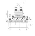
図13は、従来の半導体発光装置の断面図である。 FIG. 13 is a cross-sectional view of a conventional semiconductor light emitting device.
図13に示す半導体発光装置100は、単一の基板上に集積形成された光検出素子102と発光素子103とを有する。光検出素子102は、n型半導体層(n型基板)109と、真性半導体層110と、p型コンタクト層111とを有する。発光素子103は、p型コンタクト層111上に絶縁層112を介して形成されたp型コンタクト層113と、半導体積層膜104とを有する。半導体積層膜104は、電流狭窄層115と活性層117とを含む。発光素子103のn側電極131bは半導体積層膜104の上面に形成され、p側電極132bはp型コンタクト層113上に形成されている。光検出素子102のn側電極131aはn型半導体層109の裏面側に形成され、p側電極132aはp型コンタクト層111上に形成されている。 A semiconductor
図13に示す半導体発光装置100では、光検出素子102のPIN接合は、基板の主面に垂直方向に形成されている。活性層117から発せられたレーザ光は、基板の主面に垂直方向に出射される。活性層117から出射されるレーザ光のうち、n型半導体層109側とは反対側に出射される光が出力光として利用され、n型半導体層109側に出射される光は光検出素子102により検出される。 In the semiconductor
図13に示す半導体発光装置100では、光検出素子102の真性半導体層110と、発光素子103の活性層117との間には、2層のp型コンタクト層111,113が形成されている。このp型コンタクト層111,113には高濃度にp型不純物が導入されるため光損失が大きく、p型半導体層111,113が厚いと真性半導体層110に十分な光量が到達しない。従って、p型コンタクト層111,113は薄く設計する必要があるが、ドライエッチング工程において、p型コンタクト層111,113でストップさせるための高い精度が要求されることとなる。 In the semiconductor
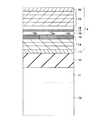
また、面発光レーザ素子を二次元アレイ上に集積するためには、隣接する面発光レーザ素子の電極を独立に設ける必要がある。そのためには、基板の裏面に電極を形成するのではなく、基板の表面に全ての電極を設けることが実装の観点からは有利である。図14は、基板の表面側に全ての電極を設けた半導体発光装置の断面図である。 Further, in order to integrate the surface emitting laser elements on the two-dimensional array, it is necessary to provide the electrodes of the adjacent surface emitting laser elements independently. For this purpose, it is advantageous from the viewpoint of mounting to provide all the electrodes on the surface of the substrate instead of forming the electrodes on the back surface of the substrate. FIG. 14 is a cross-sectional view of a semiconductor light emitting device in which all electrodes are provided on the surface side of the substrate.
図14に示す半導体発光装置100では、基板108上に形成したn型半導体層109上にn側電極131aが設けられている。n型半導体層109上にはさらに真性半導体層110が形成されており、真性半導体層110よりも上層の構成については図13に示す半導体発光装置と同様である。 In the semiconductor
しかしながら、基板の表面側にのみ電極を設けた半導体発光装置を製造する場合には、3回以上のドライエッチング工程を行う必要があり、さらに高精度なドライエッチング工程が必要とされる。この結果、歩留まりの低下に繋がる。
本発明は上記の事情に鑑みてなされたものであり、その目的は、光検出素子に到達する光量を増加させた半導体発光装置を提供することにある。
本発明の他の目的は、光検出素子および発光素子を加工するためのエッチングに要求される精度を低下させて、簡易に半導体発光装置を製造することができる半導体発光装置の製造方法を提供することにある。The present invention has been made in view of the above circumstances, and an object thereof is to provide a semiconductor light emitting device in which the amount of light reaching the light detection element is increased.
Another object of the present invention is to provide a method for manufacturing a semiconductor light-emitting device that can easily manufacture a semiconductor light-emitting device by reducing the accuracy required for etching for processing the light detection element and the light-emitting element. There is.
上記の目的を達成するため、本発明の半導体発光装置は、基板に形成され、前記基板側から順に、第1反射層と、活性層と、第2反射層とを有し、前記基板の主面に垂直方向に光を出射する発光素子と、前記基板と前記発光素子との間に形成された光検出素子とを有し、前記光検出素子は、前記基板と前記発光素子の間に形成された半導体層と、前記基板の主面に水平方向に前記半導体層の両側に形成された第1導電型領域および第2導電型領域とを有する。
この構成では、光の出射方向とは異なる方向に光検出素子の光電流が流れる。In order to achieve the above object, a semiconductor light emitting device of the present invention is formed on a substrate, andincludes a first reflective layer, an active layer, and a second reflective layer in order from the substrate side, A light emitting element that emits light in a direction perpendicular to the surface; and a light detecting element formed between the substrate and the light emitting element, wherein the light detecting element is formed between the substrate and the light emitting element. And a first conductivity type region and a second conductivity type region formed on both sides of the semiconductor layer in the horizontal direction on the main surface of the substrate.
In this configuration, the photocurrent of the light detection element flows in a direction different from the light emission direction.
上記の目的を達成するため、本発明の半導体発光装置の製造方法は、基板上に光検出素子用の半導体層を形成する工程と、前記半導体層上にコンタクト層を形成する工程と、前記コンタクト層上に発光素子用の半導体積層膜を形成する工程と、前記半導体積層膜をエッチングにより加工して、柱状の半導体積層膜のパターンを形成する工程と、前記半導体積層膜の外側のコンタクト層をエッチングにより加工して、前記半導体層を露出させる工程と、前記半導体積層膜の両側における前記半導体層の一部に、第1導電型領域および第2導電型領域を形成する工程とを有する。 In order to achieve the above object, a method for manufacturing a semiconductor light emitting device according to the present invention includes a step of forming a semiconductor layer for a photodetecting element on a substrate, a step of forming a contact layer on the semiconductor layer, and the contact Forming a semiconductor multilayer film for a light emitting element on the layer; processing the semiconductor multilayer film by etching to form a columnar semiconductor multilayer film pattern; and a contact layer outside the semiconductor multilayer film. Processing by etching to expose the semiconductor layer, and forming a first conductivity type region and a second conductivity type region in a part of the semiconductor layer on both sides of the semiconductor multilayer film.
上記の本発明の半導体発光装置の製造方法では、パターン加工した半導体積層膜の両側における半導体層の一部に、第1導電型領域および第2導電型領域を形成する。これにより、発光素子からの光の出射方向とは異なる方向に光電流が流れる光検出素子が集積形成される。 In the method for manufacturing a semiconductor light emitting device of the present invention, the first conductivity type region and the second conductivity type region are formed in a part of the semiconductor layer on both sides of the patterned semiconductor laminated film. As a result, photodetection elements in which a photocurrent flows in a direction different from the light emission direction from the light emitting elements are integrated.
本発明の半導体発光装置によれば、光検出素子に到達する光量を増加させた半導体発光装置を実現することができる。
本発明の半導体発光装置の製造方法によれば、光検出素子および発光素子を加工するためのエッチングに要求される精度を低下させて、簡易に半導体発光装置を製造することができる。According to the semiconductor light emitting device of the present invention, it is possible to realize a semiconductor light emitting device in which the amount of light reaching the light detection element is increased.
According to the method for manufacturing a semiconductor light emitting device of the present invention, it is possible to easily manufacture a semiconductor light emitting device by reducing the accuracy required for etching for processing the light detection element and the light emitting element.
以下に、本発明の実施の形態について、図面を参照して説明する。 Embodiments of the present invention will be described below with reference to the drawings.
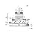
(第1実施形態)
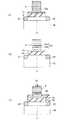
図1は、本実施形態に係る半導体発光装置1の上面図である。図2は、本実施形態に係る半導体発光装置1の断面図である。図2は、図1のA−A’線における断面図である。(First embodiment)
FIG. 1 is a top view of a semiconductor
半導体発光装置1は、基板10上に集積形成された光検出素子2と、発光素子3とを有する。 The semiconductor
GaAsからなる基板10上には、GaAsからなる真性半導体層11が形成されている。真性半導体層11上には、絶縁層12およびp型コンタクト層13が形成されている。絶縁層12およびp型コンタクト層13は、円柱状にパターン加工されている。絶縁層12はAlGaAsからなり、p型コンタクト層13はp型AlGaAsからなる。p型コンタクト層13の中央部には、半導体積層膜4が形成されている。半導体積層膜4は、円柱状にパターン加工されている。 An
絶縁層12の両側における真性半導体層11中には、n型領域(第1導電型領域)21およびp型領域(第2導電型領域)22が形成されている。これにより、基板10の主面に水平方向に光検出素子2のPIN接合が形成される。n型領域21上には、n側電極31aが形成され、p型領域22上にはp側電極32aが形成されている。n側電極31aはAuGe合金からなり、p側電極32aはTi層とAu層の積層膜からなる。 In the
円柱状のp型コンタクト層13上には、半導体積層膜4の外周を囲うようにp側電極32bがパターン形成されている。半導体積層膜4の上面には、リング状のn側電極31bが形成されている。リング状のn側電極31bの開口部が、レーザ出射口となる。n側電極31bはAuGe合金からなり、p側電極32bはTi層とAu層の積層膜からなる。 A p-
図3は、半導体積層膜4の詳細な構成を説明するための拡大断面図である。 FIG. 3 is an enlarged cross-sectional view for explaining the detailed configuration of the semiconductor laminated
半導体積層膜4は、下層から順に積層された、p型DBR(Distributed Bragg Reflector)層(第1反射層)14と、p型電流狭窄層15と、p型クラッド層16と、活性層17と、n型クラッド層18と、n型DBR層(第2反射層)19と、n型コンタクト層20とを有する。 The
p型DBR層14は、互いに組成および屈折率(n)の異なる複数種(例えば2種)のp型AlGaAs層が交互に繰り返し積層(例えば20〜40層)されて形成されている。各p型AlGaAs層の厚さをλ/4nに設定することにより、100%近い反射率をもつミラーとなる。 The p-
電流狭窄層15は、中央部のp型AlAs層15aと、p型AlAs層15aの外側の絶縁層15bとにより構成される。絶縁層15bは、p型AlAs層15aを横方向から酸化することにより形成される。このため、絶縁層15bの組成は、AlxOyである。電流狭窄層15の存在により、n側電極31bとp側電極32bに電圧を印加することにより流れる電流は、狭いp型AlAs層15aの領域のみを通る。この結果、電流閉じ込め効果が得られる。また、p型AlAs層15aの屈折率は絶縁層15bの屈折率と異なることから、光閉じ込め効果が得られる。これらの電流および光閉じ込め効果によって、しきい値電流が大幅に低減される。The
p型クラッド層16は、活性層17よりもバンドギャップの大きいp型AlGaAsからなる。活性層17は、例えば、ウェル層として機能するGaAsと、バリア層として機能するAlGaAsとを含む量子井戸構造を有する。n型クラッド層18は、活性層17よりもバンドギャップの大きいn型AlGaAsからなる。 The p-
n型DBR層19は、互いに組成および屈折率(n)の異なる複数種(例えば2種)のn型AlGaAs層が交互に繰り返し積層(例えば20〜40層)されて形成されている。各n型AlGaAs層の厚さをλ/4nに設定することにより、100%近い反射率をもつミラーとなる。n型コンタクト層20は、n型GaAsからなる。 The n-
上記の本実施形態に係る半導体発光装置1では、半導体積層膜4に順方向バイアスがかかるように、n側電極31bとp側電極32bとの間に電圧を印加することにより、活性層17から基板10の主面に垂直方向にレーザ光が出射される。リング状のn側電極31bのレーザ光出射口から出射されたレーザ光Lが出力光として利用される。一方、基板10側にもレーザ光が出射される。基板10側に出射されたレーザ光は、真性半導体層11により吸収されて、基板10の主面に水平方向に光電流Iが生じる。n型領域21およびp型領域22間を流れる光電流Iを検出することにより、レーザ光の出力がモニタリングされる。必要に応じて、光検出素子2のPIN接合に逆バイアスがかかるようにn側電極31aとp側電極32aに電圧が供給される。 In the semiconductor
本実施形態ではレーザ光が基板10の主面に垂直な方向に出射されるのに対して、光検出素子2のPIN接合が基板10の主面に平行な方向に形成されている。すなわち、レーザ光の出射方向と光検出素子2のPIN接合の方向が異なることから、レーザ光は光検出素子2のn型領域21あるいはp型領域22を通らずに真性半導体層11に吸収されて、光電流Iの発生に寄与する。すなわち、活性層17と真性半導体層11との間には、1層のp型コンタクト層13のみが存在するため、2層存在した従来例(図13および図14参照)と比較して、真性半導体層11に到達する光量を増加させることができる。この結果、光検出素子2の感度を向上させることができる。 In this embodiment, the laser light is emitted in a direction perpendicular to the main surface of the
また、基板10の一方の面側のみに全ての電極31a,31b,32a,32bが形成されていることから、発光素子3が二次元に集積した半導体発光装置1を実現することも容易となる。 In addition, since all the
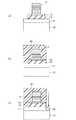
なお、基板10の一方の面側に全ての電極31a,31b,32a,32bが形成されればよく、他の電極配置を採用することもできる。図4は、他の電極配置を採用した場合における半導体発光装置1の平面図である。 It should be noted that all the
図4は、半導体積層膜4を中心として、n型領域21側およびp型領域22以外の方向(図中、縦方向)にp側電極32bのスペースを確保した例である。これにより、n型領域21とp型領域22の間の距離を縮小することができ、検出感度の向上を図ることがでできる。 FIG. 4 is an example in which a space for the p-
次に、上記の本実施形態に係る半導体発光装置1の製造方法について、図5〜図11を参照して説明する。 Next, a method for manufacturing the semiconductor
図5(a)に示すように、基板10上に、MOCVD(Metal Organic Chemical Vapor Deposition)法により、真性半導体層11と、絶縁層12と、p型コンタクト層13と、半導体積層膜4をエピタキシャル成長させる。半導体積層膜4には、p型DBR層14と、p型AlAs層15aと、p型クラッド層16と、活性層17と、n型クラッド層18と、n型DBR層19と、n型コンタクト層20が含まれる。 As shown in FIG. 5A, an
図5(b)に示すように、n型コンタクト層20上に、レジスト塗布およびリソグラフィ技術により、レジストマスク41を形成する。 As shown in FIG. 5B, a resist
図5(c)に示すように、レジストマスク41をマスクとして、半導体積層膜4をドライエッチングする。ドライエッチングでは、塩素系ガスが用いられる。このとき、p型コンタクト層13が露出するまでドライエッチングを行う。その後、図6(a)に示すように、レジストマスク41を除去する。 As shown in FIG. 5C, the
図6(b)に示すように、レジスト塗布およびリソグラフィ技術により、半導体積層膜4と半導体積層膜4の周囲のp型コンタクト層13の一部を覆うレジストマスク42を形成する。 As shown in FIG. 6B, a resist
図6(c)に示すように、レジストマスク42をマスクとして、p型コンタクト層13および絶縁層12をドライエッチングする。このとき、真性半導体層11が露出するまでドライエッチングを行う。その後、図7(a)に示すように、レジストマスク42を除去する。 As shown in FIG. 6C, the p-
図7(b)に示すように、レジスト塗布およびリソグラフィ技術により、真性半導体層11の一部を露出させるパターンのレジストマスク43を形成する。 As shown in FIG. 7B, a resist
図7(c)に示すように、不純物拡散法あるいはイオン注入法により、レジストマスク43から露出した真性半導体層11の部位にp型不純物として亜鉛を導入して、p型領域22を形成する。その後、図8(a)に示すように、レジストマスク43を除去する。 As shown in FIG. 7C, the p-
図8(b)に示すように、レジスト塗布およびリソグラフィ技術により、真性半導体層11の一部を露出させるパターンのレジストマスク44を形成する。 As shown in FIG. 8B, a resist
図8(c)に示すように、不純物拡散法あるいはイオン注入法により、レジストマスク44から露出した真性半導体層11の部位にn型不純物として珪素(Si)を導入して、n型領域21を形成する。その後、図9(a)に示すように、レジストマスク44を除去する。 As shown in FIG. 8C, silicon (Si) is introduced as an n-type impurity into the portion of the
図9(b)に示すように、半導体積層膜4の側壁から、p型AlAs層15aを横方向に部分的に酸化して、AlxOyからなる絶縁層15bを形成する。これにより、p型AlAs層15aと、絶縁層15bとからなる電流狭窄層15が形成される。As shown in FIG. 9B, the p-type AlAs
図9(c)に示すように、レジスト塗布およびリソグラフィ技術により、n側電極の配置領域以外を保護するレジストマスク45を形成する。 As shown in FIG. 9C, a resist
図10(a)に示すように、レジストマスク45、n型領域21および半導体積層膜4上にn側電極層31を形成する。n側電極層31としては、AuGe合金層を形成する。 As shown in FIG. 10A, the n-
図10(b)に示すように、リフトオフ法により、レジストマスク45とともに、レジストマスク45上のn側電極層31を除去する。これにより、n型領域21上にn側電極31aが形成され、半導体積層膜4上にn側電極31bが形成される。 As shown in FIG. 10B, the n-
図10(c)に示すように、レジスト塗布およびリソグラフィ技術により、p型電極の配置領域以外を保護するレジストマスク46を形成する。 As shown in FIG. 10C, a resist
図11(a)に示すように、p型領域22、p型コンタクト層13およびレジストマスク46上に、p側電極層32を形成する。p側電極層32は、Ti層とAu層の積層膜からなる。 As shown in FIG. 11A, the p-
図11(b)に示すように、リフトオフ法により、レジストマスク46とともに、レジストマスク46上のp側電極層32を除去する。これにより、p型領域22上にp側電極32aが形成され、p型コンタクト層13上にp側電極32bが形成される。 As shown in FIG. 11B, the p-
以上のようにして、本実施形態に係る半導体発光装置1が製造される。 As described above, the semiconductor
本実施形態に係る半導体発光装置の製造方法では、図5(c)と図6(c)に示した2回のドライエッチング工程により、半導体積層膜4のパターンと、絶縁層12およびp型コンタクト層13のパターンを作製することができる。このため、従来例(図13および図14)の場合と比べてドライエッチング工程を1回減らすことができ、製造工程を削減することができる。 In the method for manufacturing the semiconductor light emitting device according to this embodiment, the pattern of the semiconductor laminated
また、基板の主面に垂直方向にPIN接合を形成する従来例と比較して、真性半導体層11を露出させる2回目のドライエッチング工程に要求される精度は低い。このため、簡易に半導体発光装置1を作製することが可能となり、半導体発光装置1の歩留まりを向上させることができる。 In addition, the accuracy required for the second dry etching process for exposing the
(第2実施形態)
図12は、第2実施形態に係る半導体発光装置1の断面図である。(Second Embodiment)
FIG. 12 is a cross-sectional view of the semiconductor
本実施形態では、基板10上の真性半導体層11は、真性半導体からなるDBR層により形成されている。真性半導体層11上には、p型DBR層14が形成されている。真性半導体層11は、互いに組成および屈折率(n)の異なる複数種(例えば2種)のAlGaAs層が交互に繰り返し積層されて形成されている。真性半導体層11とp型DBR層14の合計の層数が、第1実施形態におけるp型DBR層14の層数と同等以上であればよい。 In the present embodiment, the
真性DBRからなる真性半導体層11上において、例えば円柱状のp型DBR層14がパターン形成されている。p型DBR層14の最上層がp型コンタクト層となる。p型DBR層14の中央部には、半導体積層膜5が形成されている。半導体積層膜5は、円柱状にパターン加工されている。半導体積層膜5は、第1実施形態で説明した半導体積層膜4のうち、p型DBR層14よりも上層の層構造に相当する。 On the
p型DBR層14の両側における真性半導体層11中には、n型領域21およびp型領域22が形成されている。これにより、基板10の主面に水平方向に光検出素子2のPIN接合が形成される。n型領域21上には、n側電極31aが形成され、p型領域22上にはp側電極32aが形成されている。n側電極31aはAuGe合金からなり、p側電極32aはTi層とAu層の積層膜からなる。 An n-
円柱状のp型DBR層14上には、p側電極32bがパターン形成されている。半導体積層膜5の上面には、リング状のn側電極31bが形成されている。リング状のn側電極31bの開口部が、レーザ出射口となる。n側電極31bはAuGe合金からなり、p側電極32bはTi層とAu層の積層膜からなる。 A p-
上記の本実施形態に係る半導体発光装置1では、半導体積層膜5に順方向バイアスがかかるように、n側電極31bとp側電極32bとの間に電圧が印加される。活性層17から発生された光は、真性半導体層11とn型DBR層14の間で繰り返し反射された後、n側電極31bの中央のレーザ出射口から出射される。基板10側に出射されたレーザ光は、ミラーを兼ねる真性半導体層11に吸収されて、基板10の主面に水平方向に光電流Iが生じる。n型領域21およびp型領域22間を流れる光電流Iを検出することにより、レーザ光の出力がモニタリングされる。必要に応じて、光検出素子2のPIN接合に逆バイアスがかかるようにn側電極31aとp側電極32aに電圧が供給される。 In the semiconductor
本実施形態では、共振器内に真性半導体層11が存在するため、第1実施形態に比べてさらに真性半導体層11に到達する光量を増加させることができる。この結果、光検出素子2の感度をさらに向上させることができる。 In the present embodiment, since the
また、基板10の一方の面側のみに全ての電極31a,31b,32a,32bが形成されていることから、発光素子3が二次元に集積した半導体発光装置1を実現することも容易となる。 In addition, since all the
なお、基板10の一方の面側に全ての電極31a,31b,32a,32bが形成されればよく、他の電極配置を採用することもできる。従って、図4で示した電極配置を採用してもよい。 It should be noted that all the
上記の本実施形態に係る半導体発光装置1は、第1実施形態で説明したエピタキシャル成長工程(図5(a))における層構成、1回目のドライエッチング工程(図5(c))の深さ、2回目のドライエッチング工程の深さ(図6(c))の深さを変えることにより製造することができる。 The semiconductor
エピタキシャル成長工程において、基板10上に真性半導体層11と、p型DBR層14と、半導体積層膜5をエピタキシャル成長させる。そして、1回目のドライエッチングにおいて、半導体積層膜5をパターン加工し、p型DBR層14を露出させる。続く、2回目のドライエッチングにおいて、p型DBR層14をパターン加工し、真性DBRからなる真性半導体層11を露出させる。以上の点以外は、第1実施形態と同様である。 In the epitaxial growth step, the
以上のようにして、本実施形態に係る半導体発光装置1が製造される。 As described above, the semiconductor
本実施形態に係る半導体発光装置の製造方法では、第1実施形態に比べて、エピタキシャル成長工程で堆積する層の膜厚を減少させることができるため、製造時間を削減することができる。 In the manufacturing method of the semiconductor light emitting device according to the present embodiment, the film thickness of the layer deposited in the epitaxial growth process can be reduced as compared with the first embodiment, so that the manufacturing time can be reduced.
本発明は、上記の実施形態の説明に限定されない。
例えば、発光素子3は、面発光レーザ以外にも面発光ダイオード(LED)であってもよい。また、本実施形態では、GaAs系材料を用いた半導体発光装置の例について説明したが、材料に限定はない。
その他、本発明の要旨を逸脱しない範囲で、種々の変更が可能である。The present invention is not limited to the description of the above embodiment.
For example, the
In addition, various modifications can be made without departing from the scope of the present invention.
1…半導体発光装置、2…光検出素子、3…発光素子、4,5…半導体積層膜、10…基板、11…真性半導体層、12…絶縁層、13…p型コンタクト層、14…p型DBR層、15…電流狭窄層、15a…p型AlAs層、15b…絶縁層、16…p型クラッド層、17…活性層、18…n型クラッド層、19…n型DBR層、20…n型コンタクト層、21…n型領域、22…p型領域、31…n側電極層、31a,31b…n側電極、32…p側電極層、32a,32b…p側電極、41,42,43,44,45,46…レジストマスク、100…半導体発光装置、102…光検出素子、103…発光素子、104…半導体積層膜、108…基板、109…n型半導体層、110…真性半導体層、111…p型コンタクト層、112…絶縁層、113…p型コンタクト層、115…電流狭窄層、117…活性層、131a,131b…n側電極、132a,132b…p側電極、L…レーザ光、I…光電流
DESCRIPTION OF
Claims (9)
Translated fromJapanese前記基板と前記発光素子との間に形成された光検出素子と
を有し、
前記光検出素子は、
前記基板と前記発光素子の間に形成された半導体層と、
前記基板の主面に水平方向に前記半導体層の両側に形成された第1導電型領域および第2導電型領域と
を有する半導体発光装置。A light emitting elementformed on a substrateand having, in order from the substrate side, a first reflective layer, an active layer, and a second reflective layer, and emitting light in a direction perpendicular to the main surface of the substrate;
A light detection element formed between the substrate and the light emitting element;
The photodetecting element is
A semiconductor layer formed between the substrate and the light emitting element;
A semiconductor light emitting device having a first conductivity type region and a second conductivity type region formed on both sides of the semiconductor layer in a horizontal direction on a main surface of the substrate.
請求項1記載の半導体発光装置。The semiconductor light emitting device according to claim 1, further comprising an insulating layer formed between the light emitting element and the light detecting element.
請求項1または2記載の半導体発光装置。Wherein the portion of the first reflective layer, a semiconductor light emitting device of claim1, wherein the semiconductor layer is formed of the light detection element.
請求項1から3の何れか一項に記載の半導体発光装置。The semiconductor light emitting device accordingto any one of claims 1to 3 , wherein the light emitting element is a surface emitting laser element.
前記半導体層上にコンタクト層を形成する工程と、
前記コンタクト層上に発光素子用の半導体積層膜を形成する工程と、
前記半導体積層膜をエッチングにより加工して、柱状の半導体積層膜のパターンを形成する工程と、
前記半導体積層膜の外側のコンタクト層をエッチングにより加工して、前記半導体層を露出させる工程と、
前記半導体積層膜の両側における前記半導体層の一部に、第1導電型領域および第2導電型領域を形成する工程と
を有する半導体発光装置の製造方法。Forming a semiconductor layer for a light detection element on a substrate;
Forming a contact layer on the semiconductor layer;
Forming a semiconductor laminated film for a light emitting element on the contact layer;
Processing the semiconductor laminated film by etching to form a columnar semiconductor laminated film pattern; and
Processing the contact layer outside the semiconductor multilayer film by etching to expose the semiconductor layer;
Forming a first conductivity type region and a second conductivity type region in a part of the semiconductor layer on both sides of the semiconductor multilayer film.
請求項5記載の半導体発光装置の製造方法。After the step of forming the first conductivity type region and the second conductivity type region, an electrode is formed on each of the semiconductor stacked film, the contact layer, the first conductivity type region, and the second conductivity type region. The method for manufacturing a semiconductor light emitting device according to claim5 , further comprising a step.
請求項5記載の半導体発光装置の製造方法。The method for manufacturing a semiconductor light emitting device according to claim5 , further comprising a step of forming an insulating layer on the semiconductor layer after the step of forming the semiconductor layer and before the step of forming the contact layer.
請求項5記載の半導体発光装置の製造方法。The method for manufacturing a semiconductor light emitting device according to claim5 , wherein an intrinsic semiconductor layer is formed in the step of forming the semiconductor layer.
請求項5記載の半導体発光装置の製造方法。The method for manufacturing a semiconductor light emitting device according to claim5 , wherein in the step of forming the semiconductor layer, a plurality of types of layers which are intrinsic semiconductors and have different refractive indexes are repeatedly stacked.
Priority Applications (1)
| Application Number | Priority Date | Filing Date | Title |
|---|---|---|---|
| JP2005294301AJP4977992B2 (en) | 2005-10-07 | 2005-10-07 | Semiconductor light emitting device and manufacturing method thereof |
Applications Claiming Priority (1)
| Application Number | Priority Date | Filing Date | Title |
|---|---|---|---|
| JP2005294301AJP4977992B2 (en) | 2005-10-07 | 2005-10-07 | Semiconductor light emitting device and manufacturing method thereof |
Publications (2)
| Publication Number | Publication Date |
|---|---|
| JP2007103811A JP2007103811A (en) | 2007-04-19 |
| JP4977992B2true JP4977992B2 (en) | 2012-07-18 |
Family
ID=38030433
Family Applications (1)
| Application Number | Title | Priority Date | Filing Date |
|---|---|---|---|
| JP2005294301AExpired - Fee RelatedJP4977992B2 (en) | 2005-10-07 | 2005-10-07 | Semiconductor light emitting device and manufacturing method thereof |
Country Status (1)
| Country | Link |
|---|---|
| JP (1) | JP4977992B2 (en) |
Families Citing this family (1)
| Publication number | Priority date | Publication date | Assignee | Title |
|---|---|---|---|---|
| JP2010177649A (en)* | 2009-02-02 | 2010-08-12 | Sony Corp | Semiconductor light emitting device |
Family Cites Families (4)
| Publication number | Priority date | Publication date | Assignee | Title |
|---|---|---|---|---|
| JPS6214465A (en)* | 1985-07-12 | 1987-01-23 | Oki Electric Ind Co Ltd | Monolithic photo-electronic integrated circuit |
| JPH0728051B2 (en)* | 1986-02-14 | 1995-03-29 | オムロン株式会社 | Semiconductor light emitting element |
| JPH02151084A (en)* | 1988-12-01 | 1990-06-11 | Matsushita Electric Ind Co Ltd | Optical semiconductor device |
| KR100587019B1 (en)* | 2005-02-25 | 2006-06-08 | 삼성전기주식회사 | Photodiode Integrated LED Package for Monitors |
- 2005
- 2005-10-07JPJP2005294301Apatent/JP4977992B2/ennot_activeExpired - Fee Related
Also Published As
| Publication number | Publication date |
|---|---|
| JP2007103811A (en) | 2007-04-19 |
Similar Documents
| Publication | Publication Date | Title |
|---|---|---|
| US8022424B2 (en) | Semiconductor device and method of manufacturing it | |
| JP4656183B2 (en) | Semiconductor light emitting device | |
| US8040934B2 (en) | Vertical cavity surface emitting laser and method of manufacturing thereof | |
| JP7683252B2 (en) | Surface emitting laser array, light source module and distance measuring device | |
| JP5447794B2 (en) | Light emitting device | |
| US8175128B2 (en) | Semiconductor laser element and semiconductor laser device | |
| US20230006421A1 (en) | Vertical cavity surface emitting laser element, vertical cavity surface emitting laser element array, vertical cavity surface emitting laser module, and method of producing vertical cavity surface emitting laser element | |
| US8073023B2 (en) | Surface emitting laser | |
| JP2010263109A5 (en) | ||
| JP4600776B2 (en) | Semiconductor laser device | |
| US20110096806A1 (en) | Semiconductor light emitting device | |
| US8194714B2 (en) | Light emitting and receiving device | |
| JP4650631B2 (en) | Semiconductor light emitting device | |
| WO1999046837A1 (en) | Surface emission laser with monitor and method of manufacturing the same | |
| JP4244058B2 (en) | Manufacturing method of semiconductor light emitting device | |
| JP4674642B2 (en) | Semiconductor light emitting device | |
| JP4977992B2 (en) | Semiconductor light emitting device and manufacturing method thereof | |
| JP5261201B2 (en) | Surface emitting laser, surface emitting laser array and manufacturing method thereof | |
| JP2010141241A (en) | Method for manufacturing light-emitting device and the light-emitting device | |
| JP2006190762A (en) | Semiconductor laser | |
| JP2008042165A (en) | Surface emitting semiconductor laser and manufacturing method thereof | |
| JP4449756B2 (en) | Optical element | |
| JP2009117599A (en) | Semiconductor light emitting device | |
| JP2007180279A (en) | Semiconductor light emitting device | |
| JP2010267642A (en) | Light emitting device |
Legal Events
| Date | Code | Title | Description |
|---|---|---|---|
| A621 | Written request for application examination | Free format text:JAPANESE INTERMEDIATE CODE: A621 Effective date:20080926 | |
| A977 | Report on retrieval | Free format text:JAPANESE INTERMEDIATE CODE: A971007 Effective date:20101101 | |
| A131 | Notification of reasons for refusal | Free format text:JAPANESE INTERMEDIATE CODE: A131 Effective date:20111122 | |
| A521 | Written amendment | Free format text:JAPANESE INTERMEDIATE CODE: A523 Effective date:20120113 | |
| TRDD | Decision of grant or rejection written | ||
| A01 | Written decision to grant a patent or to grant a registration (utility model) | Free format text:JAPANESE INTERMEDIATE CODE: A01 Effective date:20120321 | |
| A01 | Written decision to grant a patent or to grant a registration (utility model) | Free format text:JAPANESE INTERMEDIATE CODE: A01 | |
| A61 | First payment of annual fees (during grant procedure) | Free format text:JAPANESE INTERMEDIATE CODE: A61 Effective date:20120403 | |
| FPAY | Renewal fee payment (event date is renewal date of database) | Free format text:PAYMENT UNTIL: 20150427 Year of fee payment:3 | |
| LAPS | Cancellation because of no payment of annual fees |