JP4974613B2 - IC memory, access device for IC memory, and validity verification method - Google Patents
IC memory, access device for IC memory, and validity verification methodDownload PDFInfo
- Publication number
- JP4974613B2 JP4974613B2JP2006231616AJP2006231616AJP4974613B2JP 4974613 B2JP4974613 B2JP 4974613B2JP 2006231616 AJP2006231616 AJP 2006231616AJP 2006231616 AJP2006231616 AJP 2006231616AJP 4974613 B2JP4974613 B2JP 4974613B2
- Authority
- JP
- Japan
- Prior art keywords
- memory
- data
- read
- storage unit
- calculation
- Prior art date
- Legal status (The legal status is an assumption and is not a legal conclusion. Google has not performed a legal analysis and makes no representation as to the accuracy of the status listed.)
- Expired - Fee Related
Links
Images


Classifications
- G—PHYSICS
- G06—COMPUTING OR CALCULATING; COUNTING
- G06F—ELECTRIC DIGITAL DATA PROCESSING
- G06F21/00—Security arrangements for protecting computers, components thereof, programs or data against unauthorised activity
- G06F21/70—Protecting specific internal or peripheral components, in which the protection of a component leads to protection of the entire computer
- G06F21/78—Protecting specific internal or peripheral components, in which the protection of a component leads to protection of the entire computer to assure secure storage of data
- G06F21/79—Protecting specific internal or peripheral components, in which the protection of a component leads to protection of the entire computer to assure secure storage of data in semiconductor storage media, e.g. directly-addressable memories
Landscapes
- Engineering & Computer Science (AREA)
- Computer Security & Cryptography (AREA)
- Computer Hardware Design (AREA)
- Theoretical Computer Science (AREA)
- Software Systems (AREA)
- Physics & Mathematics (AREA)
- General Engineering & Computer Science (AREA)
- General Physics & Mathematics (AREA)
- Storage Device Security (AREA)
- Credit Cards Or The Like (AREA)
Description
Translated fromJapanese本発明は、RFID(Radio Frequency IdentI/Fication)タグに代表されるような複数の記憶部をもつICメモリ、及びそのようなICメモリのアクセスや制御のための技術に関する。 The present invention relates to an IC memory having a plurality of storage units represented by an RFID (Radio Frequency Ident I / Fication) tag, and a technique for accessing and controlling such an IC memory.
RFIDタグには、これまで用途にあわせて様々な仕様が存在していたが、主に流通業界での利用を目的としたUHF帯RFIDタグの規格として、例えばISO/IEC 18000-6 Type Cに準拠したRFIDタグは、複数のバンクと呼ばれる書き換え可能な記憶部を持つことができ、UIIバンクにはRFIDのIDデータを格納することができる。TIDバンクには、タグ製造メーカの情報を格納することができる。RESERVEDバンクには、パスワードデータを格納することができる。そしてUSERバンクにはオプションの領域ではあるが、各利用者が自由にデータを格納することができる。また、各バンクは、書き換えをパスワードによってロックする仕組みや、永久に書き換えを不可能にすることが可能である(非特許文献1)。
しかし、ISO/IEC 18000-6 Type Cで規定されている仕様では、RFIDタグが製造元から利用者に渡されるときのRFIDタグの内部データや書き換えのロック状態について明確な規定があるわけではない。例えばTIDバンクにRFIDタグ製造メーカがデータを書き込み永久に書き換えを不可能にしてタグを出荷することが必須になっているわけではなく、いわゆる何もデータが書かれず、後で誰でも書き換えが可能ないわゆるホワイトカードの発行も可能である。何もデータをかかなければRFIDタグの製造コストを下げることには効果的ではあるが、誰にでも自由にデータが書けるため、ホワイトカードが存在していると誰でも簡単にRFIDタグの複製ができてしまう。 However, in the specification stipulated in ISO / IEC 18000-6 Type C, there is no clear provision about the internal data of the RFID tag and the rewrite lock state when the RFID tag is delivered from the manufacturer to the user. For example, it is not mandatory for RFID tag manufacturers to write data to the TID bank and ship the data permanently, making it impossible to rewrite, so no so-called data is written, and anyone can rewrite later. A so-called white card can be issued. Although it is effective to reduce the manufacturing cost of RFID tags if no data is taken, anyone can write data freely, so anyone with a white card can easily duplicate RFID tags Can be done.
パスワードにより、データの書き換えを防ぐことも可能ではあるが、パスワードを格納するRESERVEDバンク以外のバンクは、パスワードによる書き換え制限をかけることも可能であるが、読み出すことに対しては制限がないため、読み出せれば複製ができてしまう。 Although it is possible to prevent rewriting of data with a password, banks other than the RESERVED bank that stores the password can be restricted by rewriting with a password, but there is no restriction on reading, so If it can be read, it can be copied.
従って、本発明の目的は、RFIDタグのようなICメモリにおいて、既存の仕様に影響を与えることなく、そのデータの複製を困難とすることにある。 Accordingly, an object of the present invention is to make it difficult to copy data of an IC memory such as an RFID tag without affecting existing specifications.
本発明の別の目的は、RFIDタグのようなICメモリのデータが複製された場合、それを容易に検出することを可能にすることにある。 Another object of the present invention is to make it possible to easily detect when IC memory data such as an RFID tag is duplicated.
本発明の第1の側面に従うICメモリは、複数のデータ記憶部と、外部通信装置と電波の送受信を行うためのアンテナと、前記アンテナで受信した電波上の信号の変復調の処理を行う信号処理手段と、前記信号が表すコマンド及びデータの前記外部通信装置に対する送受信、前記複数のデータ記憶部に対するデータの読み書き、及び前記ICメモリの内部状態の管理を含むプロトコル処理を行うプロトコル処理手段とを備え、前記複数のデータ記憶部のうちの少なくとも1つが、データ読出しのみが可能な読み取り専用記憶部であり、前記複数のデータ記憶部のうちの前記読み取り専用記憶部以外の記憶部が、データ読出しと書き込みのいずれもが可能な記憶部である。 The IC memory according to the first aspect of the present invention includes a plurality of data storage units, an antenna for transmitting / receiving radio waves to / from an external communication device, and signal processing for processing modulation / demodulation of signals on the radio waves received by the antenna And protocol processing means for performing protocol processing including transmission and reception of commands and data represented by the signals to and from the external communication device, reading and writing of data to and from the plurality of data storage units, and management of the internal state of the IC memory. , At least one of the plurality of data storage units is a read-only storage unit capable of only reading data, and a storage unit other than the read-only storage unit among the plurality of data storage units is configured to read data. It is a storage unit capable of both writing.
一実施形態では、前記読み取り専用記憶部が、製造後の最初の一機会又は製造時にのみデータの書き込み可能であるが、それ以降は読み取りのみが可能である。 In one embodiment, the read-only storage unit can write data only at the first opportunity after manufacture or at the time of manufacture, but can only read data thereafter.
一実施形態では、前記プロトコル処理手段が、前記複数のデータ記憶部のうちの前記読み取り専用記憶部以外の記憶部について読み取り可否または書き込み可否に関するアクセス設定を設定するデータ読出し書き込み可否設定手段と、前記設定されたアクセス設定に従って前記読み取り専用記憶部以外の記憶部の読み取りと書き込みを制御するが、前記読み取り専用記憶部については読み取りのみが行なえるアクセス制御手段とを有する。 In one embodiment, the protocol processing means is a data read / write enable / disable setting means for setting an access setting related to readability or writeability for a storage unit other than the read-only storage unit among the plurality of data storage units; According to the set access setting, the reading and writing of the storage unit other than the read-only storage unit is controlled, and the read-only storage unit includes an access control unit that can perform only reading.
一実施形態では、前記読み取り専用記憶部に、製造後の最初の一機会又は製造時のデータ書き込みによって、前記ICメモリに割り当てられた特定情報が格納されている。 In one embodiment, specific information assigned to the IC memory is stored in the read-only storage unit at the first opportunity after manufacture or data writing at the time of manufacture.
好適な実施形態では、前記読み取り専用バンクに格納された前記特定情報が、下記A〜Dの値
A 乱数値、
B 他のICメモリに割り当られた特定情報とは重複せず、かつ前記他のICメモリに割り当られた特定情報と連続関係にあるシリアル値、
C 他のICメモリに割り当られた特定情報とは重複せず、かつ前記他のICメモリに割り当られた特定情報と連続関係にない不連続値、および
D 他のICメモリに割り当られた特定情報と同一の値、
の中から選ばれた一つの値である。In a preferred embodiment, the specific information stored in the read-only bank has the following values A to D:
A random number,
B Serial value that does not overlap with the specific information assigned to the other IC memory and is in a continuous relationship with the specific information assigned to the other IC memory,
C discontinuous values that do not overlap with the specific information assigned to the other IC memory and are not in a continuous relationship with the specific information assigned to the other IC memory; and
D Same value as the specific information assigned to other IC memory,
It is one value chosen from among.
一実施形態では、前記読み取り専用バンクに格納された前記特定情報が、所定の複数のICメモリグループから選ばれた一つのICメモリグループに割り当られた、他のICメモリグループのそれとは異なるグループ識別情報と、前記選ばれた一つのICメモリグループ内で前記ICメモリに割り当てられた個別番号とを含み、前記個別番号が、下記A〜Dの値
A 乱数値、
B 前記選ばれた一つのICメモリグループ内の他のICメモリに割り当られた個別情報とは重複せず、かつ前記他のICメモリに割り当られた個別情報と連続関係にあるシリアル値、
C 前記選ばれた一つのICメモリグループ内の他のICメモリに割り当られた個別情報とは重複せず、かつ前記他のICメモリに割り当られた個別情報と連続関係にない不連続値、および
D 前記選ばれた一つのICメモリグループ内の他のICメモリに割り当られた個別情報と同一の値、
の中から選ばれた一つの値であり、前記A〜Dの値のどれが選ばれるかは、前記選ばれた一つのICメモリグループがどれであるかによって異なっている。In one embodiment, the specific information stored in the read-only bank is a group different from that of other IC memory groups assigned to one IC memory group selected from a plurality of predetermined IC memory groups. Including identification information and an individual number assigned to the IC memory in the selected one IC memory group, and the individual number is a value of the following A to D
A random number,
B Serial values that do not overlap with the individual information assigned to other IC memories in the selected one IC memory group and that are continuous with the individual information assigned to the other IC memories,
C Discrete values that do not overlap with individual information assigned to other IC memories in the selected one IC memory group and that are not continuous with individual information assigned to the other IC memory ,and
D the same value as the individual information assigned to other IC memories in the selected one IC memory group,
One of the values A to D is selected depending on which one IC memory group is selected.
一実施形態では、前記複数の記憶部のうちの前記読み取り専用記憶部以外のいずれかの記憶部に、前記読み取り専用バンクに格納された前記特定情報に対して所定の関数演算を施して得られた演算結果データが格納される。 In one embodiment, obtained by performing a predetermined function operation on the specific information stored in the read-only bank in any one of the plurality of storage units other than the read-only storage unit. The operation result data stored is stored.
一実施形態では、前記複数の記憶部のうちの前記読み取り専用記憶部以外のいずれかの記憶部に、前記読み取り専用バンクに格納された前記特定情報と他のいずれかの記憶部に格納されたデータの一部とを少なくとも含むデータに対して所定の関数演算を施して得られた演算結果データが格納される。 In one embodiment, the specific information stored in the read-only bank and the other storage unit are stored in any one of the plurality of storage units other than the read-only storage unit. Operation result data obtained by performing a predetermined function operation on data including at least a part of the data is stored.
一実施形態では、前記演算結果データが、共通鍵または公開鍵を使用した暗号演算による演算結果データである。 In one embodiment, the calculation result data is calculation result data obtained by a cryptographic calculation using a common key or a public key.
一実施形態では、ICメモリは、前記所定の関数演算を行って前記演算結果データを算出する手段を備えてない。 In one embodiment, the IC memory does not include means for performing the predetermined function calculation to calculate the calculation result data.
一実施形態では、ICメモリはRFIDであり、前記読み取り専用記憶部以外の記憶部として、RESERVEDバンク、UIIバンク、TIDバンク及びUSERバンクを有し、前記演算結果データが前記USERバンクに格納される。 In one embodiment, the IC memory is RFID, and has a RESERVED bank, a UII bank, a TID bank, and a USER bank as a storage unit other than the read-only storage unit, and the calculation result data is stored in the USER bank. .
一実施形態では、前記プロトコル処理手段が応答可能な前記読み取り専用記憶部に対する読み取りコマンドと他の記憶部に対する読み取りコマンドとが、コマンドコードにおいて異なっている。 In one embodiment, the read command for the read-only storage unit to which the protocol processing means can respond differs from the read command for the other storage unit in the command code.
一実施形態では、前記プロトコル処理手段が、前記読み取り専用記憶部の読み取り動作を行う場合と、他の記憶部の読み取り及び書き込みを行う場合とで、前記外部通信装置に対して異なるプロトコルの処理を実行する。 In one embodiment, the protocol processing means performs processing of different protocols for the external communication device depending on whether the reading operation of the read-only storage unit is performed or when reading and writing of another storage unit is performed. Execute.
本発明の第2の側面に従う外部通信装置は、上述の第1の側面に従うICメモリと通信を行なうためのものであって、前記ICメモリと電波の送受信を行うためのアンテナと、前記アンテナで受信した電波上の信号の変復調の処理を行う信号処理手段と、前記信号が表すマンド及びデータの前記ICメモリに対する送受信を含む外部通信装置プロトコルの処理を行うプロトコル処理手段と、演算対象データに所定の関数演算を行って演算結果データを算出する演算手段とを備え、前記外部通信装置プロトコル処理手段が、前記ICメモリ内の前記読み取り専用記憶部からデータを読み取る処理を行う手段と、前記読み取り専用記憶部から読み取られたデータを前記演算対象データとして前記演算手段に渡し、前記読み取られたデータに基づいて前記演算手段が算出した演算結果データを受ける手段と、前記演算手段から受けた演算結果データを、前記ICメモリ内の前記読み取り専用記憶部以外の所定の記憶部に書き込む処理を行なう手段とを有する。 An external communication device according to a second aspect of the present invention is for communicating with the IC memory according to the first aspect described above, and includes an antenna for transmitting and receiving radio waves to and from the IC memory, and the antenna. Signal processing means for performing modulation / demodulation processing of signals on received radio waves, protocol processing means for processing external communication device protocols including transmission / reception of commands and data represented by the signals to / from the IC memory, and predetermined calculation data And calculating means for calculating calculation result data, wherein the external communication device protocol processing means performs processing for reading data from the read-only storage unit in the IC memory, and the read-only Data read from the storage unit is passed to the calculation means as the calculation target data, and the calculation is performed based on the read data. A means for receiving the operation result data stage was calculated, the operation result data received from said arithmetic means, and means for performing a process of writing in a predetermined storage unit other than the read-only storage unit of the IC memory.
本発明の第3の別の側面に従う外部通信装置は、上述の第1の側面に従うICメモリと通信を行なうためのものであって、前記ICメモリと電波の送受信を行うためのアンテナと、前記アンテナで受信した電波上の信号の変復調の処理を行う信号処理手段と、前記信号が表すマンド及びデータの前記ICメモリに対する送受信を含む外部通信装置プロトコルの処理を行うプロトコル処理手段と、演算対象データに所定の関数演算を行って演算結果データを算出する演算手段とを備え、前記外部通信装置プロトコル処理手段が、前記ICメモリ内の前記読み取り専用記憶部からデータを読み取る処理を行う手段と、前記読み取り専用記憶部から読み取られたデータを前記演算対象データとして前記演算手段に渡し、前記読み取られたデータに基づいて前記演算手段が算出した演算結果データを受ける手段と、前記ICメモリ内の前記読み取り専用記憶部以外の所定の記憶部からデータを読み取る処理を行う手段と、前記演算手段から受けた演算結果データと、前記所定の記憶部から読み取られたデータとを比較することで、前記ICメモリ内のデータが正当か否かを判断する手段とを有する。 An external communication device according to a third another aspect of the present invention is for communicating with the IC memory according to the first aspect described above, and includes an antenna for transmitting and receiving radio waves to and from the IC memory, Signal processing means for processing modulation / demodulation of signals on radio waves received by an antenna, protocol processing means for processing external communication device protocols including transmission and reception of commands and data represented by the signals to and from the IC memory, and calculation target data Computing means for performing computation on a predetermined function to calculate computation result data, wherein the external communication device protocol processing means performs processing for reading data from the read-only storage unit in the IC memory, and The data read from the read-only storage unit is passed as the calculation target data to the calculation means, and the data is read based on the read data. Means for receiving calculation result data calculated by the calculation means; means for reading data from a predetermined storage unit other than the read-only storage unit in the IC memory; calculation result data received from the calculation unit; Means for determining whether or not the data in the IC memory is valid by comparing the data read from the predetermined storage unit.
上記第2又は第3の側面に従う外部通信装置の一実施形態では、前記外部通信装置プロトコル処理手段が前記ICメモリに対して送信する前記読み取り専用記憶部に対する読み取りコマンドと他の記憶部に対する読み取りコマンドとが、コマンドコードにおいて異なっているか、または、前記外部通信装置プロトコル処理手段が、前記読み取り専用記憶部の読み取り処理を行う場合と、他の記憶部の読み取り及び書き込み処理を行う場合とで、前記ICメモリに対して異なるプロトコルの処理を実行する。 In one embodiment of the external communication device according to the second or third aspect, a read command for the read-only storage unit and a read command for another storage unit that the external communication device protocol processing means transmits to the IC memory Are different in command code, or when the external communication device protocol processing means performs a read process of the read-only storage unit and a read and write process of another storage unit, Execute different protocol processing for IC memory.
本発明の第4の側面に従うシステムは、上記第1の側面に従うICメモリと、上記第2又は第3の側面に従う外部通信装置とを備える。 A system according to a fourth aspect of the present invention includes an IC memory according to the first aspect and an external communication device according to the second or third aspect.
本発明の第5の側面に従うシステムは、上記第1の側面に従うICメモリと、上記第2の側面に従う第1の外部通信装置と、上記第3の側面に従う第2の外部通信装置とを備える。 A system according to a fifth aspect of the present invention includes an IC memory according to the first aspect, a first external communication device according to the second aspect, and a second external communication device according to the third aspect. .
本発明の第6の側面に従う、上記第1の俗面に従うICメモリ内のデータの正当性を検証するための方法は、前記ICメモリ内の前記読み取り専用記憶部からデータを読み取るステップと、前記読み取り専用記憶部から読み取られたデータに所定の関数演算を施して演算結果データを得るステップと、前記ICメモリ内の前記読み取り専用記憶部以外の所定の記憶部からデータを読み取るステップと、前記演算手段から受けた演算結果データと、前記所定の記憶部から読み取られたデータとを比較することで、前記ICメモリ内のデータが正当か否かを判断するステップとを有する。 According to a sixth aspect of the present invention, there is provided a method for verifying the validity of data in an IC memory according to the first common aspect, comprising: reading data from the read-only storage unit in the IC memory; Performing a predetermined function operation on the data read from the read-only storage unit to obtain operation result data; reading data from a predetermined storage unit other than the read-only storage unit in the IC memory; Determining whether the data in the IC memory is valid by comparing the operation result data received from the means and the data read from the predetermined storage unit.
本発明の一つの側面によれば、既存の仕様に影響を与えることなく、RFIDタグのようなICメモリのデータ複製を困難にすることができる。 According to one aspect of the present invention, data replication of an IC memory such as an RFID tag can be made difficult without affecting existing specifications.
また、本発明の別の側面によれば、RFIDタグのようなICメモリのデータが複製された場合、それを容易に検出することが可能である。 Further, according to another aspect of the present invention, when data of an IC memory such as an RFID tag is duplicated, it can be easily detected.
本発明は、RFIDタグだけでなく他の種類のICメモリにも適用可能である。しかし、以下では、非限定的な説明のための例示として、RFIDタグに適用された本発明の実施形態図面を参照しながら説明していく。 The present invention is applicable not only to RFID tags but also to other types of IC memories. However, the following description will be made with reference to the drawings of an embodiment of the present invention applied to an RFID tag as an example for non-limiting explanation.
図1は、本発明の一実施形態に係るRFIDタグと、外部通信装置としての1以上のRFIDリーダライタ装置からなるRFIDシステムの構成を示した図である。 FIG. 1 is a diagram showing a configuration of an RFID system including an RFID tag according to an embodiment of the present invention and one or more RFID reader / writer devices as external communication devices.
RFIDタグ100は、或るRFIDリーダライタ装置101でデータを格納され、それとは別のRFIDリーダライタ装置102又は同じRFIDリーダライタ装置101でデータを読み取られることができる。もちろんRFIDタグ100が多数存在する場合もあるし、リーダライタ装置もより多くの台数からなるシステムもあれば、1台だけのシステムの場合もありえる。 The
図2は、RFIDタグ100の主要な内部構成を示した図である。 FIG. 2 is a diagram showing a main internal configuration of the
RFIDタグ100は、外部のRFIDリーダライタ装置と電波の送受信を行うアンテナ200と、RFIDタグ本体201と、アンテナ200で受信した電波からの動作電力の生成や、その電波に載せられる信号の変復調を行うRF部202と、その信号が表すコマンド及びデータの送受信や複数のメモリバンクに対するデータの読み書きやRFIDタグ本体201の内部状態の管理等を含むプロトコルの処理を行うRFIDタグプロトコル処理部203と、IDデータや利用者が任意に作成したデータなど各種データを記憶する記憶部204を具備する。プロトコル処理部203は、また、状態管理フラグを用いた論理的な管理方法で、記憶部204の書換え可否等のロック状態を管理する。 The
図3は、RFIDリーダライタ装置101の主要な内部構成を示した図である(他のRFIDリーダライタ装置102も同様の構成をもつ)。 FIG. 3 is a diagram showing a main internal configuration of the RFID reader / writer device 101 (other RFID reader /
RFIDリーダライタ装置101は、RFIDタグ100と電波の送受信を行うアンテナ300と、リーダライタ装置本体301と、アンテナ200で受信した電波に載せられる信号の変復調を行うRF部302と、その信号が表すコマンド及びデータの送受信やリーダライタ装置本体301の内部状態の管理等を含むプロトコルの処理を行うRFIDプロトコル処理部303と、共通鍵や公開鍵を用いての暗号や署名の演算処理や、ハッシュ関数の実施等を行う暗号処理部304と、外部の管理装置(図示省略)と連携してRFIDリーダライタ装置101が動作するための管理装置通信インタフェースとして機能する外部I/F部305を具備したものとなっている。なお、暗号処理部304は、図2に示したように、RFIDタグ100自体には備えられていない。 The RFID reader /
図4は、暗号演算処理部304で実施される暗号演算を簡単に図示したものである。 FIG. 4 simply illustrates the cryptographic operation performed by the cryptographic
暗号演算処理部304は、暗号演算関数400を有し、これは、共通鍵暗号処理や、公開鍵暗号処理など一般的によく知られたもので構わない。暗号演算関数400は、必ずしもそうでなければならないわけではないが、利用者の要求するセキュリティレベルや既存システムとの連携を考慮して変更できることが望ましい。暗号演算関数400に演算対象データ401と鍵データ402を渡すことで、暗号演算関数400による演算が実施されて、演算対象データ401に基づく暗号演算結果データ403が求められる。鍵データ402は、例えばICカードのように、暗号演算処理部304に含まれていてもよいし、或いは、外部I/F305を通じて外部装置から暗号演算関数400に渡されてもよい。暗号演算処理部304は、データを暗号化することや、データに改ざん検出のためのデータをつけることができる。鍵データ402を同一グループや利用者の中で管理することで、第3者が勝手にデータを見ることや改ざんすることを防ぐことが可能になる。鍵データ402の管理の仕方には、ICカード等で既に一般的に知られた管理方法を用いることができる。 The cryptographic
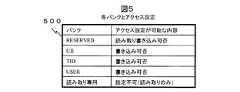
図5は、RFIDタグ100の記憶部204の構成を示したものである。 FIG. 5 shows the configuration of the
記憶部204は、この例では、5つのメモリバンク、すなわち、RESERVEDバンク、UIIバンク、TIDバンク、USERバンク及び読み取り専用バンクを有している。RESERVEDバンク、UIIバンク、TIDバンク及びUSERバンクは、RAMのように、データの書き込みと読み取りの双方が可能なメモリにより構成されている。これに対し、読み取り専用バンクは、ライトワンスメモリ又はROMのように、製造後の最初の一機会又は製造時にのみ、そこにデータを書き込むことができるが、それ以降はデータの書き込みは不可能でデータ読み取りのみが可能な構造をもつメモリであるか、或いは、RFIDプロトコル処理部203が行う論理的なアクセス制御によって、製造後の最初の一機会又は製造時にデータが書き込まれた後はデータ読み取りのみが可能になっている。読み取り専用バンクには、RFID読み取り専用バンクは、既存の規格には定義されていないものである。 In this example, the
メモリバンクの種類によりアクセス設定が可能な内容(設定により制御できるアクセスの種類)が異なっている。すなわち、RESERVEDバンクは、読み取りと書き込みのそれぞれの可否の設定が可能であるが、UIIバンク、TIDバンク、USERバンクは、書き込み可否の設定のみが可能となっている。読み取り専用バンクは、アクセス設定をすること自体が不可能である。 The contents that can be set for access (types of access that can be controlled by setting) differ depending on the type of memory bank. That is, the RESERVED bank can be set to read / write, but the UII bank, TID bank, and USER bank can only be set to write. A read-only bank cannot perform access setting itself.
各バンクのアクセス設定は、RFIDプロトコル処理部203が、それが有する内部状態保持部に、各バンクの設定値を格納することで行われる。RFIDプロトコル処理部203は、コマンド処理時に、内部状態保持部内の各バンクの設定値を参照して論理的に、各バンクのアクセスを制御することができる。読み取り専用バンクは、ライトワンスメモリで構成されて、RFIDタグ100の発行時に1回だけそこにデータが書けるようになっていてもよいし、或いは、ROMメモリにより構成されて、RFIDタグ100の製造時にそこにデータが書かれるようになっていてもよい。なお、本実施形態にかかるRFIDタグ100では、1つの記憶部204が異なるバンクに分かれているが、必ずしもバンクという概念で分かれている必要はなく、複数のバンクに代えて物理的に別の複数のメモリが設けられていてもよい。例えば読取専用バンクは、バンクではなく、他のバンクの記憶部とは物理的に別の専用の記憶部として設けられてもよく、また1つではなく、複数個存在してもよい。 The access setting of each bank is performed by the RFID
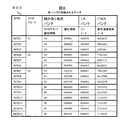
図6は、RFIDタグ100の内部データの例を示した一覧600である。 FIG. 6 is a
ここで、各RFIDタグ100は、所定の複数のRFIDグループのいずれかに分類される。そして、各RFIDタグ100には、それが分類されるRFIDグループで使用されるいずれかのRFID識別子情報といずれかのUIIデータとが割り当てられ、各RFIDタグ100内に格納される。さらに、各RFIDタグ100では、それに格納されたUIIデータの正当性を検証するためのデータが、上述した暗号演算処理部304で暗号演算結果データ403として算出され、そのデータも各RFIDタグ100内に格納される。図6は、15個の異なるRFIDタグ"RFID1"〜"RFID15"を例にとり、それらが属する複数のRFIDグループの種類と、それぞれのRFIDグループで使用されるRFID識別子情報とUIIデータの例と、UIIデータの正当性を検証するためのデータ(暗号演算結果データ403)の例と示している。 Here, each
図6に示された例では、上述したRFID識別子情報として、RFIDグループ識別情報と個別情報がある。各RFIDタグ100に割当てられたRFIDグループ識別情報と個別情報のデータは、そのRFIDタグ100内の読み取り専用バンクに格納されている。RFIDグループには、図6で"01"、"02"、"03"で示された3種類と、特定のRFIDグループに属さないこと(これも本明細書では、一つのRFIDグループとみなす)を意味する"−"で示された1種類の合計4種類があり、それぞれに対応するRFIDグループ識別情報は、"01"、"02"、"03"、"00"である。 In the example shown in FIG. 6, there are RFID group identification information and individual information as the above-described RFID identifier information. The RFID group identification information and individual information data assigned to each
さらに個別情報として、グループ"01"では、互いに重複することのないシリアルな番号、例えば"000001"、"000002"、"000003"などが使用される。グループ"02"では、互いに重複することのない不連続な(シリアルでない)番号、例えば"000001"、"000002"、"000004"などが使用される。グループ"02"では、個別情報がシリアルであることを保障しないことで、不具合品の除去を簡単に可能とすることができ、RFIDタグを安価に製造することが可能になる。グループ"03"では、乱数値、例えば"146236"、"492528"、"660318"などが使用される。グループ"03"では、個別情報が乱数であるため重複する可能性はあるが、個別情報を管理する必要がなく、また個別情報のデータ長を大きくすれば重複の可能性が非常に低くなるため、安価なRFIDタグの製造に向いている。グループ"−"ではすべてという一つの特別の値、例えば"000000"が使用される。グループ"−"は、既存の仕様のRFIDタグと同様の使い方をしたいだけの利用者のためのグループであり、そこでは、個別情報"000000"が設定されていれば、RFID識別情報を使う必要はなく、或いは、個別情報を使用せずにRFIDグループ識別情報"00"だけを使用してもよい。個別情報としての特別値は、"000000"でなくても、例えば"111111"のように別の特別値であってもよい。 Furthermore, serial numbers that do not overlap each other, such as “000001”, “000002”, and “000003”, are used as the individual information in the group “01”. In the group “02”, discontinuous (non-serial) numbers that do not overlap each other, for example, “000001”, “000002”, “000004”, and the like are used. In the group “02”, since it is not guaranteed that the individual information is serial, the defective product can be easily removed, and the RFID tag can be manufactured at low cost. In the group “03”, random values such as “146236”, “492528”, “660318”, and the like are used. In the group “03”, there is a possibility of duplication because the individual information is a random number. However, it is not necessary to manage the individual information, and if the data length of the individual information is increased, the possibility of duplication becomes very low. Suitable for manufacturing inexpensive RFID tags. The group "-" uses one special value, for example "000000", all. The group “−” is a group for users who only want to use the RFID tag of the existing specification. In this case, if individual information “000000” is set, it is necessary to use the RFID identification information. Alternatively, only the RFID group identification information “00” may be used without using individual information. The special value as the individual information may not be “000000” but may be another special value such as “111111”.
また、図6は、UIIバンクに格納されるUIIデータの例も示している。この例では、いずれのRFIDグループでも、他のグループと共通のUIIデータ、例えば"00000001"、"00000002","00000003"などが使用される。また、図6は、UIIデータの正当性を検証するためのデータとして、USERバンクに格納される暗号演算結果データ403の例も示している。この例では、暗号演算結果データ403を求めるための演算対象データ401として、"RFIDグループ識別情報"と"個別情報"と"UIIデータ"を結合したものを用いている。異なるRFIDタグのUIIデータが同じ値、例えば"00000001"、であっても、それらのRFIDタグが属するRFIDグループが異なれば、それらのRFIDタグの暗号演算結果データ403は異なる値となる。ただし、RFIDグループ"−"内では、いずれのRFIDタグも、RFIDグループ識別情報と個別情報にて同じであるため、異なるRFIDタグのUIIデータが同じである場合は、それらのRFIDタグの暗号演算結果データも同じになる。 FIG. 6 also shows an example of UII data stored in the UII bank. In this example, any RFID group uses UII data common to other groups, for example, “00000001”, “00000002”, “00000003”, and the like. FIG. 6 also shows an example of cryptographic operation result data 403 stored in the USER bank as data for verifying the validity of UII data. In this example, “RFID group identification information”, “individual information”, and “UII data” are combined as the
図7は、RFIDタグ100に送信される通常の読み取りコマンド(つまり、読み取り専用バンク以外のバンクに対する読み取りコマンド)のフォーマットの例と、RFIDタグ100からRFIDリーダライタ装置101又は102へ返信される、通常の読み取りコマンドに対する応答のフォーマットの例を示す。 FIG. 7 shows an example of the format of a normal read command (that is, a read command for a bank other than the read-only bank) transmitted to the
通常の読み取りコマンドは、コマンドフォーマット700に示すように、"Command"というコマンドコード値を格納するフィールド、"MemBank"という読み取り対象のバンクを指定するパラメータを格納するフィールド、及び"WordPtr"というポインタの種類を指定するパラメータを格納するフィールドなどから構成される。 As shown in the
通常の読み取りコマンドに対する応答は、応答フォーマット701に示すように、ヘッダを格納するフィールド、及び"Memory Word"という読み出されたデータを格納するフィールドなどから構成される。 A response to a normal read command includes a field for storing a header and a field for storing read data “Memory Word”, as shown in a response format 701.
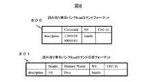
図8は、RFIDリーダライタ装置101又は102からRFIDタグ100に送信される読み取り専用バンクに対する読み取りコマンドのフォーマットの例と、RFIDタグ100からRFIDリーダライタ装置101又は102へ返信される、読み取り専用バンクに対する読み取りコマンドに対する応答のフォーマットの例を示す。 FIG. 8 shows an example of a read command format for a read-only bank transmitted from the RFID reader /
読み取り専用バンクに対する読み取りコマンドは、コマンドフォーマット800に示すように、"Command"というコマンドコード値を格納するフィールドと、その他のパラメータを格納するフィールドなどから構成される。このコマンドフォーマット800は、図7に示した通常の読み取りコマンドのコマンドフォーマット700とは、コマンドコード値やパラメータが全く異なった構成となっている。このようなカスタムコマンドを使うことで、既存の仕様に影響を与えることがない。 As shown in the
図9は、二つの異なるプロトコルに対応したRFIDタグ部をもつRFIDタグ100の構成例を示す。 FIG. 9 shows a configuration example of an
RFIDタグ100は、第1のプロトコルに対応する第1のRFIDタグ部(例えばISO18000-6 Type Cに準拠したRFIDタグとして機能する部分)と、第2のプロトコルに対応する第2のRFIDタグ部(例えば2.45Ghz帯のプロトコルに対応したRFIDタグとして機能する部分)とを備える。第1のRFIDタグ部は、そこに記憶されたデータの書換えが可能であるが、第2のRFIDタグ部は、そこに記憶されたデータの書換えは不可能であり、読み取りのみが可能である。 The
第1のRFIDタグ部は、RFIDリーダライタ装置と電波の送受信を行うアンテナ900と、第1のRFIDタグ本体901と、アンテナ900で受信した電波からの動作電力の生成や、その電波に載せられる信号の変復調を行うRF部902と、その信号が表すコマンド及びデータの送受信や、後述の書き換え可能記憶部904内の複数のメモリバンクに対するデータの読み書きや、第1のRFIDタグ本体901の内部状態の管理等を含むプロトコルの処理を行うRFIDタグプロトコル処理部903と、IDデータや利用者データなど各種データを記憶する書き換え可能記憶部904とを具備する。書き換え可能記憶部904内に、前述したRESERVEDバンク、UIIバンク、TIDバンク及びUSERバンクが設けられる。 The first RFID tag unit generates an operating power from the
第2のRFIDタグ部はRFIDリーダライタ装置と電波の送受信を行うアンテナ905と、第2のRFIDタグ本体906と、アンテナ905で受信した電波からの動作電力の生成や、その電波に載せられる信号の変復調を行うRF部907と、その信号が表すコマンド及びデータの送受信や、後述の読み取り専用記憶部909に対するデータの読み書きや、第2のRFIDタグ本体906の内部状態の管理等を含むプロトコルの処理を行うRFIDタグプロトコル処理部908と、RFIDグループ識別情報データや個別情報などを格納する読み取り専用の記憶部909を具備する。読み取り専用の記憶部909が、前述した読み取り専用バンクとして使用される。読み取り専用の記憶部909へのアクセスは、他のメモリバンクとは異なるプロトコル、すなわち既存のRFIDタグ用の規格に従う第1のプロトコルとは異なる第2のプロトコルで行われる必要がある。 The second RFID tag unit includes an
変形例として、RFIDタグ100が3つ以上のRFIDタグ部を備えてもよいし、或いは、まったく同じプロトコルに対応した複数のRFIDタグ部を備えてもよい。 As a modification, the
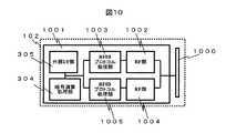
図10は、図9に示したような二つの異なるプロトコルに対応するRFIDタグと通信可能なRFIDリーダライタ装置の内部構成の例を示す。 FIG. 10 shows an example of the internal configuration of an RFID reader / writer device capable of communicating with RFID tags corresponding to two different protocols as shown in FIG.
RFIDリーダライタ装置102は、RFIDタグ100との電波の送受信を行うアンテナ1000と、リーダライタ装置本体1001と、第1のプロトコルのコマンド及びデータを表した信号の変復調を行うRF部1002と、第1のプロトコルのコマンド及びデータの送受信や第1のプロトコル上でのRFIDリーダライタ装置102の内部状態の管理等を含むプロトコルの処理を行うRFIDプロトコル処理部1003と、第2のプロトコルのコマンド及びデータを表した信号の変復調を行うRF部1004と、第2のプロトコルのコマンド及びデータの送受信や第2のプロトコル上でのRFIDリーダライタ装置102の内部状態の管理等を含むプロトコルの処理を行うRFIDプロトコル処理部1005と、共通鍵や公開鍵を用いての暗号や署名の演算処理や、ハッシュ関数の実施等を行う暗号処理部304と、外部の管理装置(図示省略)と連携して動作するための管理装置インタフェースとして機能する外部I/F部305を具備したものとなっている。この例では、分かり易くするために、異なるプロトコルについて異なるRF部と異なるプロトコル処理部が備えられているが、変形例として、異なるプロトコルについての処理が共通の一つのRF部と一つのプロトコル処理部で行われるようになっていてもよい。 The RFID reader /
図10に示された構成をもつRFIDリーダライタ装置102であれば、図9に示された構成のRFIDタグ100内の書き換え可能記憶部904と読み取り専用記憶部909のそれぞれのデータを異なるプロトコルにより取り扱うことが可能である。その際、読み取りコマンドや応答のフォーマットは、それぞれのプロトコルに適合した合致したものが使用される。 In the case of the RFID reader /
図11は、利用者がRFIDタグ100内のUIIデータの正当性を検証するための処理フロー例を示した図である。 FIG. 11 is a diagram illustrating an example of a processing flow for the user to verify the validity of the UII data in the
ここでは、RFIDタグ100が、図6に例示されたRFIDグループ"01"に属する1つのRFIDタグ"RFID1"である場合を想定する。しかし、これは説明のための非限定的な例示であり、RFIDタグ100がRFIDグループ"01"〜"03"に属するいずれのRFIDタグであってもよい。 Here, it is assumed that the
図11の処理は、RFIDタグ100の利用者が必要に応じて何時でも実行できるものである。この処理が開始されるより前に、RFIDタグ100の読み取り専用バンクにRFIDグループ識別情報"01"と個別情報"000001"が格納され、UIIバンクにはUIIデータ"00000001"が格納されている。これらの格納行為を行う主体に格別の限定は無いが、典型例を示せば、読み取り専用バンクにRFIDグループ識別情報"01"と個別情報"000001"を格納する行為は、例えばRFIDタグ100のメーカによって、RFIDタグ100の出荷前に行われる。また、UIIデータ"00000001"の格納行為は、例えば、利用者によって行われ得る。そして、UIIデータ"00000001"を格納した利用者は、そのUIIデータの正当性を保証したければ、UIIデータの正当性を検証するため暗号演算結果データを、RFIDタグ100に格納することができる。 The process of FIG. 11 can be executed at any time by the user of the
図11に示された前半の処理フローは、上記のような利用者が、UIIデータの正当性を検証するための暗号演算結果データをRFIDタグ100に格納するための処理を示している。よって、図11の処理フローの開始時点では、上記暗号演算結果データは未だRFIDタグ100に格納されていない。 The process flow of the first half shown in FIG. 11 shows a process for the user as described above to store the cryptographic operation result data for verifying the validity of the UII data in the
図11の前半の処理フローにおいて、ステップS1100で、上記利用者が使用するRFIDリーダライタ装置101と、RFIDタグ100との間で、RFIDタグ100内のUIIデータを読み取る処理が実行される。すなわち、RFIDリーダライタ装置101からRFIDタグ100へ、UIIバンク読み取りコマンドが送付される。そして、RFIDタグ100からRFIDリーダライタ装置101へ、UIIデータ"00000001"が応答される。 In the process flow of the first half of FIG. 11, in step S1100, a process of reading UII data in the
その後のステップS1101で、RFIDリーダライタ装置101とRFIDタグ100との間で、RFIDタグ100内の読み取り専用バンク内のRFID識別情報を読み取る処理が実行される。すなわち、すなわち、RFIDリーダライタ装置101からRFIDタグ100へ、読み取り専用バンクに対する読み取りコマンドが送付される。そして、RFIDタグ100からRFIDリーダライタ装置101へ、読み取り専用バンクから読み出されたRFIDグループ識別情報"01"と個別情報"000001"が応答される。 In subsequent step S1101, a process of reading the RFID identification information in the read-only bank in the
その後、ステップS1102で、RFIDリーダライタ装置101にて、暗号演算処理が実行される。すなわち、RFIDタグ100から読み出したRFIDグループ識別情報"01"、個別情報"000001"及びUIIデータ"00000001"を結合したデータが、演算対象データ401として暗号演算関数400に渡され、暗号演算関数400が暗号演算結果データ403として、UIIデータの正当性を検証するためのデータ"4624652"を導く。鍵データ402や暗号演算関数400の具体的な例示はここでは省略するが、これらは、RFIDグループ識別情報"01"を使う利用者により管理される。 Thereafter, in step S1102, the RFID reader /
その後、ステップS1103で、上記暗号演算結果データ"4624652"の書き込み処理が実行される。すなわち、RFIDリーダライタ装置101がRFIDタグ100へ、上記暗号演算結果データ"4624652"をUSERバンクに書き込むための書き込みコマンドを送る。RFIDタグ100は、その書き込みコマンドを受けて、USERバンクに、読み取り専用バンクのRFID識別情報を活用したUII検証用のデータ"4624652"を格納する。 Thereafter, in step S1103, the cryptographic calculation result data “4624652” is written. That is, the RFID reader /
以上のようにして、UII検証用のデータ"4624652"が格納された後、もし、このRFIDタグ100が流通業界で利用されているのならば、このRFIDタグ100は他の種々の利用者へ転々と流通されていくであろう。この流通過程で、鍵データ402や暗号演算関数400を利用できる権限をもつ利用者は、RFIDリーダライタ装置102を用いて、RFIDタグ100内のUIIデータが正当なデータかどうか(換言すれば、RFIDタグ100が、他のRFIDタグの複製でないかどうかを)を、図11の後半の処理フローで検証することができる。 After the UII verification data “4626462” is stored as described above, if the
すなわち、まず、S1104で、RFIDリーダライタ装置102とRFIDタグ100との間で、UIIデータの読み取り処理が実行される。すなわち、RFIDリーダライタ装置102からRFIDタグ100へ、UIIバンク読み取りコマンドが送付され、RFIDタグ100からRFIDリーダライタ装置102へ、UIIデータ"00000001"が応答される。 That is, first, in S1104, UII data reading processing is executed between the RFID reader /
その後、ステップS1105で、RFID識別情報の読み取り処理が実行される。すなわち、RFIDリーダライタ装置102からRFIDタグ100へ、読み取り専用バンクに対する読み取りコマンドが送付されて、RFIDタグ100からRFIDリーダライタ装置102へ、RFIDグループ識別情報"01"と個別情報"000001"が応答される。 Thereafter, in step S1105, the RFID identification information reading process is executed. That is, a read command for the read-only bank is sent from the RFID reader /
その後、ステップS1106で、暗号演算処理が実行される。すなわち、RFIDリーダライタ装置102内で、演算対象データ401としてのRFIDグループ識別情報"01"、個別情報"000001"及びUIIデータ"00000001"が暗号演算関数400に渡され、暗号演算関数400が暗号演算結果データ403として、UIIデータの正当性を検証するためのデータ"4624652"を導く。 Thereafter, in step S1106, cryptographic operation processing is executed. That is, in the RFID reader /
その後(又は、ステップS1104〜S1106の何れかより前でもよい)、ステップS1107で、USERバンクに格納されている暗号演算結果データの読み取り処理が実行される。すなわち、RFIDリーダライタ装置102からRFIDタグ100へ、USERバンク読み取りコマンドが送付されて、RFIDタグ100からRFIDリーダライタ装置102へ、暗号演算結果データ"4624652"が応答される。 Thereafter (or may be before any of steps S1104 to S1106), in step S1107, the cryptographic operation result data stored in the USER bank is read. That is, a USER bank read command is sent from the RFID reader /
その後、ステップS1108で、演算対象データの正当性検証処理が実行される。すなわち、RFIDリーダライタ装置102内で、RFIDプロトコル処理部が、ステップS1106で演算された暗号演算結果データと、ステップS1107で読み出された暗号演算結果データとを比較し、両者が一致していれば、RFIDタグ100内のUIIデータは正当なデータであると判断する。一方、両者が一致しない場合には、第3者がRFIDタグ100内のデータを改ざんしたか、複製した等の可能性が考えられるから、RFIDリーダライタ装置102は、エラーを利用者に通知する。なお、鍵データ402を知らない第3者は、正しい暗号演算結果データを求めることができないため、RFIDタグ100内のUIIデータの正当性の検証を行なうことはできない。この検証は、正当な利用者だけが、それを必要とするときにだけ行えばよい。通常のUIIデータの読み取りは、既存の仕様に従うプロトコルだけで何の問題もなく実行することができる。 After that, in step S1108, the validity verification process for the calculation target data is executed. That is, in the RFID reader /
このように、上述した本発明の実施形態によれば、既存の仕様に影響を与えることなく、RFIDタグのデータ複製を困難にし、さらに、そのデータが複製された場合、上記検証によって容易にそのことの検出が可能である。 As described above, according to the above-described embodiment of the present invention, it is difficult to duplicate the data of the RFID tag without affecting the existing specifications. Further, when the data is duplicated, it is easily confirmed by the above verification. Can be detected.
100 RFIDタグ
101 RFIDリーダライタ装置A
102 RFIDリーダライタ装置
200 RFIDタグアンテナ
201 RFIDタグ本体
202 RF部
203 RFIDプロトコル処理部
204 記憶部
300 RFIDリーダライタ装置アンテナ
301 RFIDリーダライタ装置本体
302 RF部
303 RFIDプロトコル処理部
303 暗号演算処理部
400 暗号演算関数
401 演算対象データ
402 鍵データ
403 演算結果データ
500 各バンクとアクセス設定の一覧
501 異なるグループのRFIDタグに格納されるデータの一覧
700 通常Readコマンドフォーマット
701 通常Readコマンド応答フォーマット
800 読み取り専用バンク通常Readコマンドフォーマット
801 読み取り専用バンク通常Readコマンド応答フォーマット
900 RFIDタグアンテナ
901 RFIDタグ本体
902 RF部
903 RFIDプロトコル処理部
904 書き換え可能記憶部
905 アンテナ
906 RFIDタグ本体
907 RF部
908 RFIDプロトコル処理部
909 書き換え可能記憶部
1000 RFIDリーダライタ装置アンテナ
1001 RFIDリーダライタ装置本体
1002 RF部
1003 RFIDプロトコル処理部
1004 RF部
1005 RFIDプロトコル処理部100
102 RFID reader /
Claims (16)
Translated fromJapanese外部通信装置と電波の送受信を行うためのアンテナと、
前記アンテナで受信した電波上の信号の変復調の処理を行う信号処理手段と、
前記信号が表すコマンド及びデータの前記外部通信装置に対する送受信、前記複数のデータ記憶部に対するデータの読み書き、及び自身の内部状態の管理を含むプロトコル処理を行うプロトコル処理手段と
を備え、
前記複数のデータ記憶部のうちの少なくとも1つが、ライトワンスな読み取り専用記憶部であり、
前記複数のデータ記憶部のうちの前記読み取り専用記憶部以外の記憶部が、データ読出しと書き込みのいずれもが可能な記憶部であり、
前記プロトコル処理手段が応答可能な前記読み取り専用記憶部に対する読み取りコマンドと他の記憶部に対する読み取りコマンドとが異なっていて、
前記他の記憶部に対する読み取りコマンドは、当該読み取りコマンドのコマンドコード値と前記複数のデータ記憶部のいずれかを指定するパラメータとポインタの種類を指定するパラメータとからなるフィールドを有し、前記読み取り専用記憶部に対する読み取りコマンドは、前記他の記憶部の読み取りコマンドとは異なるコマンドコード値からなり、前記フィールドとは異なるコマンドフィールドを有する
ことを特徴とするICメモリ。A plurality of data storage units;
An antenna for transmitting and receiving radio waves to and from an external communication device;
Signal processing means for performing modulation / demodulation processing of signals on radio waves received by the antenna;
Protocol processing means for performing protocol processing including transmission and reception of commands and data represented by the signals to and from the external communication device, reading and writing of data to and from the plurality of data storage units, and management ofits own internal state,
At least one of the plurality of data storage units is awrite-once read-only storage unit,
The storage unit other than the read-only storage unit of the plurality of data storage unit,Ri storage unit der any of the possible data read andwrite,
The read command for the read-only storage unit to which the protocol processing means can respond is different from the read command for the other storage unit,
The read command for the other storage unit has a field including a command code value of the read command, a parameter for specifying one of the plurality of data storage units, and a parameter for specifying a pointer type, and the read command The IC memory, wherein a read command for the storage unit has a command code value different from the read command for the other storage unit, and has a command field different from the field .
前記読み取り専用記憶部が、製造後の最初の一機会にのみデータの書き込みが可能であるが、それ以降は読み取りのみが可能であることを特徴とするICメモリ。The IC memory according to claim 1, wherein
IC memory said read-only storage section, is a data canbe written onlyto the first one occasion after manufacture, characterized in that thereafter it can only read.
前記読み取り専用記憶部に、製造後の最初の一機会のデータ書き込みによって、前記ICメモリから読み出されて当該ICメモリの正当性を検証するための特定情報が格納されている
ことを特徴とするICメモリ。The IC memory accordingto claim 1or 2 ,
The read-only memory unit, the data writingfor the first one occasion after manufacture, identification informationfor being read from said IC memoryto verify the validity of the IC memory, wherein the stored IC memory.
前記読み取り専用記憶部に格納された前記特定情報が、下記A〜Dの値
A 乱数値、
B 他のICメモリから読み出された特定情報とは重複せず、かつ前記他のICメモリから読み出された特定情報と連続関係にあるシリアル値、
C 他のICメモリから読み出された特定情報とは重複せず、かつ前記他のICメモリから読み出された特定情報と連続関係にない不連続値、および
D 他のICメモリから読み出された特定情報と同一の値、
の中から選ばれた一つの値である
ことを特徴とするICメモリ。The IC memory according to claim3 , wherein
The specific information stored in the read-onlystorage unit is a value of the following A to D
A random number,
B does not overlap with the specificinformation read from the other IC memory, and serial number in continuous relationship with the identification informationread from said other IC memory,
C discontinuous values that do not overlap with the specific informationread from the other IC memory and are not in a continuous relationship withthe specific informationread from the other IC memory, and
D Same value as specific informationread from other IC memory
IC memory characterized by being one value selected from among the above.
前記読み取り専用記憶部に格納された前記特定情報が、
所定の複数のICメモリグループから選ばれた一つのICメモリグループに割り当られた、他のICメモリグループのそれとは異なるグループ識別情報と、
前記選ばれた一つのICメモリグループ内で前記ICメモリに割り当てられた個別番号と
を含み、
前記個別番号が、下記A〜Dの値
A 乱数値、
B 前記選ばれた一つのICメモリグループ内の他のICメモリに割り当てられた個別情報とは重複せず、かつ前記他のICメモリに割り当てられた個別情報と連続関係にあるシリアル値、
C 前記選ばれた一つのICメモリグループ内の他のICメモリに割り当てられた個別情報とは重複せず、かつ前記他のICメモリに割り当てられた個別情報と連続関係にない不連続値、および
D 前記選ばれた一つのICメモリグループ内の他のICメモリに割り当てられた個別情報と同一の値、
の中から選ばれた一つの値であり、
前記A〜Dの値のどれが選ばれるかが、前記選ばれた一つのICメモリグループがどれであるかによって異なっている
ことを特徴とするICメモリ。The IC memory according to claim3 , wherein
The specific information stored in the read-onlystorage unit is
Group identification information different from that of other IC memory groups assigned to one IC memory group selected from a plurality of predetermined IC memory groups,
And an individual number assigned to the IC memory within the selected one IC memory group,
The individual number is a value of the following A to D
A random number,
B is a serial value that does not overlap with the individual information assigned to the other IC memory in the selected one IC memory group and that is continuous with the individual information assigned to the other IC memory,
C discrete values that do not overlap with the individual information assigned to other IC memories in the selected one IC memory group and are not in a continuous relationship with the individual information assigned to the other IC memories, and
D the same value as the individual information assigned to other IC memories in the selected one IC memory group,
Is one value chosen from
IC memory Which one is selected, characterized in that <br/> said one IC memory group selected isthat different depending on which of the values of the to D.
前記複数の記憶部のうちの前記読み取り専用記憶部以外のいずれかの記憶部に、前記読み取り専用記憶部に格納された前記特定情報に対して所定の関数演算を施して得られた、前記ICメモリの正当性を検証するためのデータである演算結果データが格納される
ことを特徴とするICメモリ。In the IC memory according to any one of claims 3 to5 ,
TheIC obtained by performing a predetermined function operation on the specific information stored in the read-onlystorage unit in any one of the plurality of storage units other than the read-onlystorage unit An IC memory characterized in that operation result data,which is data for verifying the validity of the memory, is stored.
前記複数の記憶部のうちの前記読み取り専用記憶部以外のいずれかの記憶部に、前記読み取り専用記憶部に格納された前記特定情報と他のいずれかの記憶部に格納されたデータの一部とを少なくとも含むデータに対して所定の関数演算を施して得られた、前記ICメモリの正当性を検証するためのデータである演算結果データが格納される
ことを特徴とするICメモリ。In the IC memory according to any one of claims 3 to5 ,
The specific information stored in the read-onlystorage unit and apart of the data stored in any other storage unit in any one of the plurality of storage units other than the read-onlystorage unit An IC memory characterized in that operation result data,which is data for verifying the validity of the IC memory, obtained by performing a predetermined function operation on data including at least
前記演算結果データが、共通鍵または公開鍵を使用した暗号演算による演算結果データである
ことを特徴とするICメモリ。The IC memory according to claim6 or7 ,
An IC memory, wherein the calculation result data is calculation result data obtained by a cryptographic calculation using a common key or a public key.
前記所定の関数演算を行って前記演算結果データを算出する手段を備えてない
ことを特徴とするICメモリ。The IC memory according to any one of claims6 to 8 ,
An IC memory, comprising no means for performing the predetermined function calculation and calculating the calculation result data.
前記ICメモリはRFIDであり、
前記読み取り専用記憶部以外の記憶部として、RESERVEDバンク、UIIバンク、TIDバンク及びUSERバンクを有し、
前記演算結果データが前記USERバンクに格納される
ことを特徴とするICメモリ。The IC memory according to any one of claims6 to 9 ,
The IC memory is RFID,
As a storage unit other than the read-only storage unit, it has a RESERVED bank, a UII bank, a TID bank, and a USER bank,
An IC memory, wherein the operation result data is stored in the USER bank.
前記ICメモリと電波の送受信を行うためのアンテナと、
前記アンテナで受信した電波上の信号の変復調の処理を行う信号処理手段と、
前記信号が表すコマンド及びデータの前記ICメモリに対する送受信を含む外部通信装置プロトコルの処理を行うプロトコル処理手段と、
演算対象データに所定の関数演算を行って演算結果データを算出する演算手段と
を備え、
前記外部通信装置プロトコル処理手段が、
前記ICメモリ内の前記読み取り専用記憶部からデータを読み取る処理を行う手段と、
前記読み取り専用記憶部から読み取られたデータを前記演算対象データとして前記演算手段に渡し、前記読み取られたデータに基づいて前記演算手段が算出した演算結果データを受ける手段と、
前記演算手段から受けた演算結果データを、前記ICメモリ内の前記読み取り専用記憶部以外の所定の記憶部に書き込む処理を行なう手段と
を有する
ことを特徴とする外部通信装置。In the external communication apparatus which communicates with IC memory as described in any one of Claims1-10 ,
An antenna for transmitting and receiving radio waves to and from the IC memory;
Signal processing means for performing modulation / demodulation processing of signals on radio waves received by the antenna;
And protocol processing means for processing the external communication device protocols, including transmission and reception with respect to the IC memorycommands and data to which the signal is represented,
A calculation means for calculating a calculation result data by performing a predetermined function calculation on the calculation target data;
The external communication device protocol processing means is
Means for reading data from the read-only storage in the IC memory;
Means for passing data read from the read-only storage unit to the calculation means as the calculation target data and receiving calculation result data calculated by the calculation means based on the read data;
An external communication apparatus comprising: means for performing a process of writing calculation result data received from the calculation means into a predetermined storage unit other than the read-only storage unit in the IC memory.
前記ICメモリと電波の送受信を行うためのアンテナと、
前記アンテナで受信した電波上の信号の変復調の処理を行う信号処理手段と、
前記信号が表すマンド及びデータの前記ICメモリに対する送受信を含む外部通信装置プロトコルの処理を行うプロトコル処理手段と、
演算対象データに所定の関数演算を行って演算結果データを算出する演算手段と
を備え、
前記外部通信装置プロトコル処理手段が、
前記ICメモリ内の前記読み取り専用記憶部からデータを読み取る処理を行う手段と、
前記読み取り専用記憶部から読み取られたデータを前記演算対象データとして前記演算手段に渡し、前記読み取られたデータに基づいて前記演算手段が算出した演算結果データを受ける手段と、
前記ICメモリ内の前記読み取り専用記憶部以外の所定の記憶部からデータを読み取る処理を行う手段と、
前記演算手段から受けた演算結果データと、前記所定の記憶部から読み取られたデータとを比較することで、前記ICメモリ内のデータが正当か否かを判断する手段と
を有する
ことを特徴とする外部通信装置。In the external communication apparatus which communicates with IC memory as described in any one of Claims1-10 ,
An antenna for transmitting and receiving radio waves to and from the IC memory;
Signal processing means for performing modulation / demodulation processing of signals on radio waves received by the antenna;
Protocol processing means for processing an external communication device protocol including transmission / reception of the command and data represented by the signal to and from the IC memory;
A calculation means for calculating a calculation result data by performing a predetermined function calculation on the calculation target data;
The external communication device protocol processing means is
Means for reading data from the read-only storage in the IC memory;
Means for passing data read from the read-only storage unit to the calculation means as the calculation target data and receiving calculation result data calculated by the calculation means based on the read data;
Means for reading data from a predetermined storage unit other than the read-only storage unit in the IC memory;
Comparing the calculation result data received from the calculation means with the data read from the predetermined storage unit to determine whether the data in the IC memory is valid or not External communication device.
前記外部通信装置プロトコル処理手段が前記ICメモリに対して送信する前記読み取り専用記憶部に対する読み取りコマンドと他の記憶部に対する読み取りコマンドとが、コマンドコード値において異なっているか、または、
前記外部通信装置プロトコル処理手段が、前記読み取り専用記憶部の読み取り処理を行う場合と、他の記憶部の読み取り及び書き込み処理を行う場合とで、前記ICメモリに対して異なるプロトコルの処理を実行する
ことを特徴とする外部通信装置。The external communication device according to claim11 or 12 ,
The read command for the read-only storage unit that the external communication device protocol processing means transmits to the IC memory and the read command for the other storage unit are different in command codevalues , or
The external communication device protocol processing means executes processing of different protocols for the IC memory depending on whether to read the read-only storage unit or to read and write to another storage unit. An external communication device characterized by that.
請求項11〜13のいずれか一項記載の1以上の外部通信装置と
を備えたシステム。The IC memory according to any one of claims 1 to10 ,
A system comprising one or more external communication devices according to claim11 .
請求項11記載の第1の外部通信装置と、
請求項12記載の第2の外部通信装置と
を備えたシステム。The IC memory according to any one of claims 1 to10 ,
A first external communication device according to claim11 ;
A system comprising: the second external communication device according to claim12 .
前記外部装置は、
前記ICメモリと電波の送受信を行うためのアンテナと、
前記アンテナで受信した電波上の信号の変復調の処理を行う信号処理手段と、
前記信号が表すコマンド及びデータの前記ICメモリに対する送受信を含む外部通信装置プロトコルの処理を行うプロトコル処理手段と、
演算対象データに所定の関数演算を行って演算結果データを算出する演算手段と
を備え、
前記プロトコル処理手段が、
前記ICメモリ内の前記読み取り専用記憶部からデータを読み取るステップと、
前記読み取ったデータを前記演算対象データとして前記演算手段に渡すステップと
を有し、
前記演算手段が、
読み取り専用記憶部から受け取ったデータに所定の関数演算を施して演算結果データを得るステップと、
前記演算結果データを前記プロトコル処理手段に渡すステップと
を有し、
前記プロトコル処理手段が、さらに、
前記ICメモリ内の前記読み取り専用記憶部以外の所定の記憶部からデータを読み取るステップと、
前記演算手段から受けた演算結果データと、前記所定の記憶部から読み取られたデータとを比較することで、前記ICメモリ内のデータが正当か否かを判断するステップと
を有する方法。
A method for verifying validity of data in the IC memoryby an external communication device that communicates with the IC memory according to claim 1 ,
The external device is
An antenna for transmitting and receiving radio waves to and from the IC memory;
Signal processing means for performing modulation / demodulation processing of signals on radio waves received by the antenna;
Protocol processing means for processing an external communication device protocol including transmission and reception of the command and data represented by the signal to the IC memory;
A calculation means for calculating a calculation result data by performing a predetermined function calculation on the calculation target data;
With
The protocol processing means comprises:
Reading data from the read-only storage in the IC memory;
Passing the read data to the calculation means as the calculation target data;
Have
The computing means is
Performing a predetermined function operation on the data received from the read-only storage unit to obtain operation result data;
Passing the operation result data to the protocol processing means;
Have
The protocol processing means further comprises:
Reading data from a predetermined storage unit other than the read-only storage unit in the IC memory;
A method of determining whether or not the data in the IC memory is valid by comparing the calculation result data received from the calculation means with the data read from the predetermined storage unit.
Priority Applications (3)
| Application Number | Priority Date | Filing Date | Title |
|---|---|---|---|
| JP2006231616AJP4974613B2 (en) | 2006-08-29 | 2006-08-29 | IC memory, access device for IC memory, and validity verification method |
| EP07252994AEP1916546A3 (en) | 2006-08-29 | 2007-07-30 | IC memory, as well as, accessing apparatus and validity testing method for use of IC memory |
| US11/830,982US20080094183A1 (en) | 2006-08-29 | 2007-07-31 | Ic memory, as well as, accessing apparatus and validity testing method for use of ic memory |
Applications Claiming Priority (1)
| Application Number | Priority Date | Filing Date | Title |
|---|---|---|---|
| JP2006231616AJP4974613B2 (en) | 2006-08-29 | 2006-08-29 | IC memory, access device for IC memory, and validity verification method |
Publications (2)
| Publication Number | Publication Date |
|---|---|
| JP2008059013A JP2008059013A (en) | 2008-03-13 |
| JP4974613B2true JP4974613B2 (en) | 2012-07-11 |
Family
ID=39182083
Family Applications (1)
| Application Number | Title | Priority Date | Filing Date |
|---|---|---|---|
| JP2006231616AExpired - Fee RelatedJP4974613B2 (en) | 2006-08-29 | 2006-08-29 | IC memory, access device for IC memory, and validity verification method |
Country Status (3)
| Country | Link |
|---|---|
| US (1) | US20080094183A1 (en) |
| EP (1) | EP1916546A3 (en) |
| JP (1) | JP4974613B2 (en) |
Families Citing this family (11)
| Publication number | Priority date | Publication date | Assignee | Title |
|---|---|---|---|---|
| WO2006115374A1 (en)* | 2005-04-25 | 2006-11-02 | Lg Electronics Inc. | Reader control system |
| CN101246538A (en)* | 2007-02-14 | 2008-08-20 | 日电(中国)有限公司 | Radio frequency recognition system and method |
| JP4521678B2 (en)* | 2007-11-19 | 2010-08-11 | フェリカネットワークス株式会社 | COMMUNICATION SYSTEM, INFORMATION PROCESSING METHOD, PROGRAM, AND INFORMATION PROCESSING DEVICE |
| US7795895B2 (en)* | 2007-11-28 | 2010-09-14 | Mstar Semiconductor, Inc. | Loop-back testing method and apparatus for IC |
| US8712334B2 (en) | 2008-05-20 | 2014-04-29 | Micron Technology, Inc. | RFID device using single antenna for multiple resonant frequency ranges |
| US9208360B2 (en) | 2008-06-04 | 2015-12-08 | Electronics And Telecommunications Research Institute | RFID tag for RFID service and RFID service method thereof |
| US8320570B2 (en)* | 2008-12-05 | 2012-11-27 | Electronics And Telecommunications Research Institute | Apparatus and method for generating secret key |
| JP5398845B2 (en)* | 2009-11-24 | 2014-01-29 | 三菱電機株式会社 | Information processing apparatus and program |
| KR101139726B1 (en) | 2010-10-04 | 2012-04-26 | 인크로스 주식회사 | method for extending UII region by using user memory region in RFID tag |
| JP5991160B2 (en)* | 2012-11-19 | 2016-09-14 | ソニー株式会社 | Disc cartridge and changer |
| US10149135B1 (en)* | 2017-05-30 | 2018-12-04 | Illinois Tool Works Inc. | Methods and apparatuses for wireless communication with a brush |
Family Cites Families (11)
| Publication number | Priority date | Publication date | Assignee | Title |
|---|---|---|---|---|
| US5036461A (en)* | 1990-05-16 | 1991-07-30 | Elliott John C | Two-way authentication system between user's smart card and issuer-specific plug-in application modules in multi-issued transaction device |
| DE4205567A1 (en)* | 1992-02-22 | 1993-08-26 | Philips Patentverwaltung | METHOD FOR CONTROLLING ACCESS TO A STORAGE AND ARRANGEMENT FOR IMPLEMENTING THE METHOD |
| JPH09282433A (en)* | 1996-04-12 | 1997-10-31 | Nhk Spring Co Ltd | Security system |
| US7239226B2 (en)* | 2001-07-10 | 2007-07-03 | American Express Travel Related Services Company, Inc. | System and method for payment using radio frequency identification in contact and contactless transactions |
| US6957333B2 (en)* | 2002-09-12 | 2005-10-18 | Symbol Technologies, Inc. | System and method for encrypted communications between electronic devices |
| US20050049979A1 (en)* | 2003-08-26 | 2005-03-03 | Collins Timothy J. | Method, apparatus, and system for determining a fraudulent item |
| JP4664035B2 (en)* | 2004-10-18 | 2011-04-06 | シャープ株式会社 | Functional IC tag |
| US7960719B2 (en)* | 2004-12-03 | 2011-06-14 | Semiconductor Energy Laboratotry Co., Ltd. | Semiconductor device |
| JP4954537B2 (en)* | 2004-12-03 | 2012-06-20 | 株式会社半導体エネルギー研究所 | Semiconductor device |
| WO2006115374A1 (en)* | 2005-04-25 | 2006-11-02 | Lg Electronics Inc. | Reader control system |
| US20070194879A1 (en)* | 2005-05-02 | 2007-08-23 | International Business Machines Corporation | Method and device for detecting an invalid RFID tag and method for manufacturing an RFID tag |
- 2006
- 2006-08-29JPJP2006231616Apatent/JP4974613B2/ennot_activeExpired - Fee Related
- 2007
- 2007-07-30EPEP07252994Apatent/EP1916546A3/ennot_activeWithdrawn
- 2007-07-31USUS11/830,982patent/US20080094183A1/ennot_activeAbandoned
Also Published As
| Publication number | Publication date |
|---|---|
| EP1916546A2 (en) | 2008-04-30 |
| EP1916546A3 (en) | 2011-09-07 |
| JP2008059013A (en) | 2008-03-13 |
| US20080094183A1 (en) | 2008-04-24 |
Similar Documents
| Publication | Publication Date | Title |
|---|---|---|
| JP4974613B2 (en) | IC memory, access device for IC memory, and validity verification method | |
| CN108053001B (en) | Information security authentication method and system for electronic warehouse receipt | |
| US8610538B2 (en) | Memory-tag data authentication | |
| US7872567B2 (en) | Method for transponder access control | |
| AU2006203517B2 (en) | Using Promiscuous and Non-Promiscuous Data to Verify Card and Reader Identity | |
| US20090033464A1 (en) | Transponder with access protection and method for access to the transponder | |
| US7302572B2 (en) | Portable information storage medium and its authentication method | |
| US9317981B2 (en) | Method and device for protecting products against counterfeiting | |
| EP2474936A1 (en) | Product identity digital identification apparatus, inspection apparatus, product and anti-counterfeiting inspection method | |
| US20230273988A1 (en) | Systems and methods for authentication | |
| US10007815B2 (en) | Production method, RFID transponder, authentication method, reader device and computer program product | |
| KR20040085800A (en) | contactless type communication tag and portable tag reader for verifying a genuine article | |
| US20060010302A1 (en) | Non-contact IC recording medium, recording medium managing program, and recording medium managing method | |
| US20110119497A1 (en) | Smart card and access method thereof | |
| Yamamoto et al. | A tamper detection method for RFID tag data | |
| US20090040023A1 (en) | RF Transponder for Off-Line Authentication of a Source of a Product Carrying the Transponder | |
| JP2008233975A (en) | Information communication device, information central management device, and information processing system | |
| Lehtonen et al. | Serialized TID numbers-A headache or a blessing for RFID crackers? | |
| EP0982687A1 (en) | Method for preventing or detecting fraud in an identification system | |
| KR20110111661A (en) | RDF tag for copy protection, copy protection system and method using same | |
| EP2495690B1 (en) | Transponder and method for monitoring access to application data in the transponder | |
| WO2009005296A2 (en) | System and method for processing certification of digital contents and computer-readable medium having thereon program performing function embodying the same | |
| CN115066684B (en) | Method for verifying radio frequency identification number | |
| TWI894202B (en) | Apparatus and method for validating radio frequency identification number | |
| KR101023558B1 (en) | Dynamic Partitioned RFID Memory Access Method, RFID ID Tags, and RFID Terminals and Recording Media |
Legal Events
| Date | Code | Title | Description |
|---|---|---|---|
| A621 | Written request for application examination | Free format text:JAPANESE INTERMEDIATE CODE: A621 Effective date:20090402 | |
| A977 | Report on retrieval | Free format text:JAPANESE INTERMEDIATE CODE: A971007 Effective date:20111228 | |
| A131 | Notification of reasons for refusal | Free format text:JAPANESE INTERMEDIATE CODE: A131 Effective date:20120110 | |
| A521 | Request for written amendment filed | Free format text:JAPANESE INTERMEDIATE CODE: A523 Effective date:20120312 | |
| TRDD | Decision of grant or rejection written | ||
| A01 | Written decision to grant a patent or to grant a registration (utility model) | Free format text:JAPANESE INTERMEDIATE CODE: A01 Effective date:20120410 | |
| A01 | Written decision to grant a patent or to grant a registration (utility model) | Free format text:JAPANESE INTERMEDIATE CODE: A01 | |
| A61 | First payment of annual fees (during grant procedure) | Free format text:JAPANESE INTERMEDIATE CODE: A61 Effective date:20120410 | |
| R150 | Certificate of patent or registration of utility model | Free format text:JAPANESE INTERMEDIATE CODE: R150 | |
| FPAY | Renewal fee payment (event date is renewal date of database) | Free format text:PAYMENT UNTIL: 20150420 Year of fee payment:3 | |
| LAPS | Cancellation because of no payment of annual fees |