JP4972444B2 - Vapor growth apparatus and vapor growth method - Google Patents
Vapor growth apparatus and vapor growth methodDownload PDFInfo
- Publication number
- JP4972444B2 JP4972444B2JP2007093133AJP2007093133AJP4972444B2JP 4972444 B2JP4972444 B2JP 4972444B2JP 2007093133 AJP2007093133 AJP 2007093133AJP 2007093133 AJP2007093133 AJP 2007093133AJP 4972444 B2JP4972444 B2JP 4972444B2
- Authority
- JP
- Japan
- Prior art keywords
- gas
- flow path
- wafer
- chamber
- vapor phase
- Prior art date
- Legal status (The legal status is an assumption and is not a legal conclusion. Google has not performed a legal analysis and makes no representation as to the accuracy of the status listed.)
- Expired - Fee Related
Links
- 238000000034methodMethods0.000titleclaimsdescription19
- 239000007789gasSubstances0.000claimsdescription170
- 238000001947vapour-phase growthMethods0.000claimsdescription24
- 230000015572biosynthetic processEffects0.000claimsdescription21
- 230000002093peripheral effectEffects0.000claimsdescription17
- 238000004140cleaningMethods0.000claimsdescription16
- BUMGIEFFCMBQDG-UHFFFAOYSA-NdichlorosiliconChemical compoundCl[Si]ClBUMGIEFFCMBQDG-UHFFFAOYSA-N0.000claimsdescription14
- 239000012535impuritySubstances0.000claimsdescription14
- BLRPTPMANUNPDV-UHFFFAOYSA-NSilaneChemical compound[SiH4]BLRPTPMANUNPDV-UHFFFAOYSA-N0.000claimsdescription5
- 229910000077silaneInorganic materials0.000claimsdescription4
- SLLGVCUQYRMELA-UHFFFAOYSA-NchlorosiliconChemical compoundCl[Si]SLLGVCUQYRMELA-UHFFFAOYSA-N0.000claimsdescription3
- ZDHXKXAHOVTTAH-UHFFFAOYSA-NtrichlorosilaneChemical compoundCl[SiH](Cl)ClZDHXKXAHOVTTAH-UHFFFAOYSA-N0.000claimsdescription3
- 239000005052trichlorosilaneSubstances0.000claimsdescription3
- 239000012159carrier gasSubstances0.000claimsdescription2
- 239000004065semiconductorSubstances0.000description12
- 239000013078crystalSubstances0.000description11
- OAICVXFJPJFONN-UHFFFAOYSA-NPhosphorusChemical compound[P]OAICVXFJPJFONN-UHFFFAOYSA-N0.000description5
- 229910052698phosphorusInorganic materials0.000description5
- 239000011574phosphorusSubstances0.000description5
- 229910004298SiO 2Inorganic materials0.000description4
- 229910021421monocrystalline siliconInorganic materials0.000description4
- XYFCBTPGUUZFHI-UHFFFAOYSA-NPhosphineChemical compoundPXYFCBTPGUUZFHI-UHFFFAOYSA-N0.000description3
- ZOXJGFHDIHLPTG-UHFFFAOYSA-NBoronChemical compound[B]ZOXJGFHDIHLPTG-UHFFFAOYSA-N0.000description2
- 229910052782aluminiumInorganic materials0.000description2
- 229910052796boronInorganic materials0.000description2
- 229910021420polycrystalline siliconInorganic materials0.000description2
- 239000000758substrateSubstances0.000description2
- 238000007740vapor depositionMethods0.000description2
- YCKRFDGAMUMZLT-UHFFFAOYSA-NFluorine atomChemical compound[F]YCKRFDGAMUMZLT-UHFFFAOYSA-N0.000description1
- GYHNNYVSQQEPJS-UHFFFAOYSA-NGalliumChemical compound[Ga]GYHNNYVSQQEPJS-UHFFFAOYSA-N0.000description1
- 229910001218Gallium arsenideInorganic materials0.000description1
- 229910000530Gallium indium arsenideInorganic materials0.000description1
- 230000005856abnormalityEffects0.000description1
- XAGFODPZIPBFFR-UHFFFAOYSA-NaluminiumChemical compound[Al]XAGFODPZIPBFFR-UHFFFAOYSA-N0.000description1
- 229910052785arsenicInorganic materials0.000description1
- 150000001875compoundsChemical class0.000description1
- 229910052731fluorineInorganic materials0.000description1
- 239000011737fluorineSubstances0.000description1
- 229910052733galliumInorganic materials0.000description1
- 229910052739hydrogenInorganic materials0.000description1
- 239000001257hydrogenSubstances0.000description1
- 125000004435hydrogen atomChemical class[H]*0.000description1
- 238000004519manufacturing processMethods0.000description1
- 229910000073phosphorus hydrideInorganic materials0.000description1
- 229910052710siliconInorganic materials0.000description1
- 239000010703siliconSubstances0.000description1
- 239000000126substanceSubstances0.000description1
- 230000007704transitionEffects0.000description1
- 239000012808vapor phaseSubstances0.000description1
Images

Landscapes
- Crystals, And After-Treatments Of Crystals (AREA)
- Chemical Vapour Deposition (AREA)
Description
Translated fromJapanese本発明は、チャンバー内のウェハ上にシリコンなどの半導体層を気相成長により形成する気相成長装置及び気相成長方法に関する。 The present invention relates to a vapor phase growth apparatus and a vapor phase growth method for forming a semiconductor layer such as silicon on a wafer in a chamber by vapor phase growth.
従来、ウェハに成膜する製造装置として、気相成長装置(CVD:Chemical
Vapor Depositionで、この中にVPE:Vapor phase epitaxial growthを含む)が一般的で、例えば特開平9−17734号公報(特許文献1)に示すように、Siの成膜では、ガスとしてシラン(SiH4)またはジクロロシラン(SiH2Cl2)ガスと水素(H2)が用いられている。
なお、ここで、基板の性質によっては、単結晶SiまたはポリSi膜が形成されるが、Si単結晶基板には通常、単結晶Si膜が成膜される。Conventionally, as a manufacturing apparatus for forming a film on a wafer, a vapor deposition apparatus (CVD: Chemical)
In Vapor Deposition, VPE (including Vapor phase epitaxial growth) is generally used. For example, as shown in Japanese Patent Laid-Open No. 9-17734 (Patent Document 1), in Si film formation, silane (SiH4 ) or dichlorosilane (SiH2 Cl2 ) gas and hydrogen (H2 ).
Here, depending on the properties of the substrate, a single crystal Si or poly Si film is formed, but a single crystal Si film is usually formed on the Si single crystal substrate.
具体的な例としては、図2に示す通りで、支持台201上に載置された半導体ウェハ202がチャンバ203内に収納される。収納された半導体ウェハ202は、ヒータ204により、成膜に必要な温度に加熱される。
チャンバ203には、ジクロロシラン(SiH2Cl2)ガス(或いはSiH4ガス)及びH2ガスを供給するガス流路205a、205b(第1の流路)が連結され、ガス流路の他方はそれぞれガスシリンダ206a、206bに接続されている。その流路205a、205bの途中には、ガスを開閉するバルブ207a、207bが接続されている。As a specific example, as shown in FIG. 2, a
シリンダ206a、206bより、ガス流路205a、205bを介し、バルブ207a、207bが開放され、流路200を介して、チャンバ203内に、ジクロロシラン(SiH2Cl2)ガス(或いはSiH4ガス)、H2ガスが供給され、半導体ウェハ上に、単結晶Si膜が成膜される。この成膜は、何回か繰り返して行う場合が多い。例えば特開2000−282241号公報に示す如く、ジクロロシラン(SiH2Cl2)ガス(或いはSiH4ガス)に硼素、アルミニウム、ガリウム及び燐などを含むようにすると、P型、N型の半導体単結晶層を形成可能である。更に、特開2004−281673号公報(特許文献2)の如く、SiH4ガスと、O2ガスを供給するようにすれば、SiO2膜が、SiN4ガスとHN3ガスなどを供給するようにすれば、Si3N4膜が成膜できる。Valves 207a and 207b are opened from the
また、チャンバ203には、ClF3ガス(SiO2膜、Si3N4膜の場合CF4やC2F6などのガスを用いる)を供給するガス流路208が接続され、その流路208の途中には、ガスを開閉するバルブ209が接続されている。The
成膜(単結晶Si膜)が終了後、チャンバ203内をクリーニングする際、シリンダ210より、ガス流路208を介し、バルブ209を開放することにより、ClF3ガスが供給される(バルブ207a及び207bは閉じてある)。
なお、上記ウェハ上への成膜、チャンバ内のクリーニングにおいて、ガスの排気は、バルブ211を開放して、ガス排気用のガス流路212の接続されている真空ポンプ213より、バキュームされる。When the inside of the
In the film formation on the wafer and the cleaning of the chamber, the exhaust of the gas is vacuumed by the
ところで、上述した図2の気相成長装置において、成膜時に用いるジクロロシラン(SiH2Cl2)ガス(或いはSiH4ガス)と、クリーニング時に用いるClF3ガスとの混合を、危険性などから絶対に避ける必要がある。
このため、特に成膜時に用いるジクロロシラン(SiH2Cl2)ガス(或いはSiH4ガス)を流す流路205aに接続されているバルブ307a、307bを、クリーニング時に完全に閉めるようにしている。また、成膜が完了後、N2などで、チャンバ内をパージし、その後、バルブ211を開き、排出用のガス流路212に接続されている真空ポンプ213でバキュームし、ジクロロシラン(SiH2Cl2)ガス(或いはSiH4ガス)を完全に排気するようにしている。By the way, in the above-described vapor phase growth apparatus of FIG. 2, mixing of dichlorosilane (SiH2 Cl2 ) gas (or SiH4 gas) used at the time of film formation and ClF3 gas used at the time of cleaning is absolutely necessary because of danger. Need to be avoided.
For this reason, in particular, the valves 307a and 307b connected to the
上記の気相成長装置を用いて、半導体ウェハ上にSi単結晶膜が成膜される。しかし、その成膜の膜厚が、半導体ウェハの中央部と周辺部とでバラツキがあると共に、成膜された膜における、不純物濃度も中央部と周縁部で異なり、改良すべきことが多くあった。
そこで、その1つとして、ヒータの温度をきめ細かく制御し、膜厚を一定にする方法があるが、膜厚制御において充分でないのが実情である。A Si single crystal film is formed on a semiconductor wafer using the vapor phase growth apparatus. However, the film thickness of the deposited film varies between the central part and the peripheral part of the semiconductor wafer, and the impurity concentration in the deposited film differs between the central part and the peripheral part, so there are many cases that should be improved. It was.
Therefore, as one of the methods, there is a method of finely controlling the temperature of the heater to make the film thickness constant, but the actual situation is that the film thickness control is not sufficient.
上述したように、従来の気相成長装置においては、半導体ウェハ上に成膜される膜厚が一定ではなく、また、不純物濃度にもバラつきがあり、未だ改良すべき点があった。
本発明は、上記した点に対処して鑑みなされ、半導体ウェハ上に成膜される膜を略均一に、そして不純物濃度のバラツキも少なくした新規な気相成長装置及び気相成長方法を提供することにある。As described above, in the conventional vapor phase growth apparatus, the film thickness formed on the semiconductor wafer is not constant, and the impurity concentration varies, and there are still points to be improved.
The present invention has been made in view of the above points, and provides a novel vapor phase growth apparatus and vapor phase growth method in which a film formed on a semiconductor wafer is substantially uniform and variation in impurity concentration is reduced. There is.
本発明の気相成長装置は、チャンバ内にウェハ載置用の支持台が収容され、前記ウェハ上に成膜するための第一のガスを供給する第一の流路及び前記ウェハ上に成膜される膜の不純物濃度を制御するための第二のガスを供給する第二の流路が前記チャンバに接続された気相成長装置において、
前記第一の流路は、シラン(SiH4)ガス、トリクロルシラン(SiHCl3)ガスまたはジクロロシラン(SiH2Cl2)ガスを供給するガス流路Aと、キャリアガスを供給するガス流路Bと、クリーニングガスを供給するガス流路Cとからなり、このガス流路A、ガス流路Bおよびガス流路Cが合流してプロセスガス流路を形成し、このプロセスガス流路は、少なくとも2系統に分割され、前記チャンバに接続されて、ウェハ上の周辺部と中央部に前記第一のガスが個々に供給されるように構成されており、かつ前記ガス流路A、前記ガス流路B、および前記ガス流路Cには、ガスの流通を制御するバルブがそれぞれ設けられており、前記ガス流路Aのバルブよりチャンバ側流路および前記ガス流路Bのバルブよりチャンバ側流路に圧力センサが設けられ、これらの圧力センサが圧力上昇を感知した際には、前記流路Cのバルブを閉鎖するように設定されており、
前記第二の流路は、少なくとも2経路に分割され、前記ウェハ上の周辺部と中央部に、前記第二のガスが個々に供給されるように構成されていることを特徴とする。
In the vapor phase growth apparatus of the present invention,a support for mounting a wafer is accommodated in achamber, and a first flow path for supplying a first gasfor film formation on the wafer is formed on the wafer. In the vapor phase growth apparatus in which the second flow path for supplying the second gas for controlling the impurity concentration of the film to be formed is connected to the chamber,
The first flow path includesa gas flow path A for supplyingsilane (SiH4) gas, trichlorosilane (SiHCl3) gas or dichlorosilane (SiH2Cl2) gas, and a gas flow path B for supplying carrier gas. And a gas flow path C for supplying a cleaning gas, and the gas flow path A, the gas flow path B, and the gas flow path C merge to form a process gas flow path. The system is divided into two systems, connected to the chamber, and configured to individually supply the first gas to the peripheral part and the central part on the wafer, and the gas flow path A, the gas flow The passage B and the gas flow path C are each provided with a valve for controlling the flow of gas, the chamber side flow path from the gas flow path A valve and the valve side of the gas flow path B to the chamber side. Road pressure sensor provided on these when the pressure sensor senses a pressure rise is set to close the valve of the flow path C,
The second flow path is divided into at least two paths, and the second gas is individually supplied to a peripheral part and a central part on the wafer.
また、本発明の好ましい態様は、上述した第一の流路が3経路1a、1b,1c、第二の流路が3経路2a,2b,2cに分割され、ウェハ上の周辺部、中腹部及び中央部に、個々に供給されるように構成されていることを特徴とする。
この気相成長装置において、支持台には、ヒータが設けられ、このヒータがウェハの周辺部、中腹部、中央部に対応して設けられていることが望ましい。
In a preferred embodiment of the present invention, the first flow path described above is divided intothree paths 1a, 1b, 1c, and the second flow path is divided intothree paths 2a, 2b, 2c. And it is comprised so that it may be separately supplied to a center part.
In this vapor phase growth apparatus, it is desirable that a heater is provided on the support base, and that this heater is provided corresponding to the peripheral portion, middle portion, and central portion of the wafer.
さらに、本発明の特徴とする気相成長方法は、チャンバ内に、支持台上に載置されたウェハが収容され、ウェハ上に成膜するためのガスを供給する第一の流路及びウェハ上に成膜される膜の不純物濃度を制御するためのガスを供給する第二の流路がチャンバに接続された気相成長装置を用いてウェハに気相成長を行う際、上述した第一の流路及び前記第二の流路を、夫々2経路1a、1b及び2経路2a,2bに分割し、夫々の経路1a,1b,2a,2bのガスを制御して、ウェハ上の周辺部と中央部の膜厚及び不純物濃度を制御することを特徴とする。 Furthermore, in the vapor phase growth method characterized by the present invention, a wafer placed on a support base is accommodated in a chamber, and a first flow path for supplying a gas for film formation on the wafer and the wafer When performing vapor phase growth on a wafer using a vapor phase growth apparatus in which a second flow path for supplying a gas for controlling the impurity concentration of a film formed thereon is connected to the chamber, And the second flow path are divided into two paths 1a, 1b and two paths 2a, 2b, respectively, and the gas on each path 1a, 1b, 2a, 2b is controlled to provide a peripheral portion on the wafer. And controlling the film thickness and impurity concentration in the central portion.
本発明によれば、半導体ウェハ上に均一な成膜が可能で、また、成膜中の不純物濃度のバラツキも少なくなり、結果的に歩留まりの高い成長が可能となる。 According to the present invention, uniform film formation on a semiconductor wafer is possible, and variation in impurity concentration during film formation is reduced, and as a result, growth with a high yield is possible.
以下、本発明の実施の形態について、図面を参照して詳細に説明する。 Hereinafter, embodiments of the present invention will be described in detail with reference to the drawings.
(実施形態1)
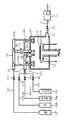
第1の実施形態では、上述した従来例と同様で、図1に示す如く、支持台101上に載置されたSi単結晶ウェハ102がチャンバ103内に収納される。収納されたSi単結晶ウェハ102は、ヒータ104により、成膜に必要な温度例えば1100度に加熱される。このヒータ104はウェハ102の中央部に相当する部分と、周辺部に相当する部分に分離し、個々に制御するようにした方が望ましい。縦型のエピタキシャル成長装置の場合は、インヒータとアウトヒータに相当する。(Embodiment 1)
In the first embodiment, similar to the conventional example described above, a Si
チャンバ103には、シラン(SiH4)ガス或いはトリクロルシラン(SiHCl3)ガスまたはジクロロシラン(SiH2Cl2)ガス、及びH2ガスを供給するガス流路105a、105bを介して、第1の流路となるプロセスガスを供給するガス流路121に接続される。ガス流路105a、105bの他方は、それぞれガスシリンダ106a、106bに接続されている。その流路105a、105bの途中には、ガスを開閉するバルブ107a、107bが接続されている。上述の第1の流路となるガス流路121は、チャンバ103の上部の中央部と周辺部に分岐121a、121b1及び121b2に接続されている。このように構成することにより、ウェハ102への供給を制御可能となる。このプロセスガスの制御は、プロセスガス制御部122で行うことができる。A silane (SiH4 ) gas, a trichlorosilane (SiHCl3 ) gas, a dichlorosilane (SiH2 Cl2 ) gas, and a H2 gas are supplied to the
なお、ここで、ウェハ102の中央部と周辺部に供給できるように、2つに分岐させているが、さらに制御を行う必要がある場合、3つ即ち中央部と周辺部の間にガスが供給できるようにしても良い。このように3つに分岐すれば、さらなる膜厚制御が可能となる。 In addition, here, it is branched into two so that it can be supplied to the central portion and the peripheral portion of the
また、第2の流路となるガス流路131は、第1のガス流路121と同様にフォスフィン(PH3)シリンダ117からリンを含むガスが、ガス流路105c、バルブ107cを介してチャンバ103内に供給される。この場合も、上記プロセスガスの供給と同様に、ガス流路131は2つに分岐131a、131b1及び131b2されている。このように構成すれば、リンを含むガスが、ウェハ102の中央部と周辺部に供給できるようになり、ウェハの不純物濃度を制御可能となる。このリンを含むガスの制御は、リンのガス制御部132で行うことができる。なお、ここで、ウェハ102の中央部と周辺部に供給できるように、2つに分岐させているが、さらに制御を行う必要がある場合、プロセスガス制御と同様に、3つ即ち中央部と周辺部の間にガスが供給できるようにしても良い。このように3つに分岐すれば、さらなる膜厚制御が可能となる。Similarly to the first
なお、この実施形態の場合、不純物濃度を制御するガスとして、フォスフィン(PH3)を用いたが、硼素を含むガスB2H6を用いても良く、他のガスAlやAsを含むガスを用いても構わない。In this embodiment, phosphine (PH3 ) is used as a gas for controlling the impurity concentration. However, a gas B2 H6 containing boron may be used, and a gas containing other gases Al or As is used. You may use.
シリンダ106a、106bより、ガス流路105a、105bを介し、バルブ107a、107bが開放され、また、シリンダ117から、ガス流路105cを介してバルブ107cが開放され、ガス流路121,131を経由してチャンバ103内に、SiH4ガス或いはジクロロシラン(SiH2Cl2)ガス、H2ガス、PH3ガスが供給され、Si単結晶ウェハ102上に、Si単結晶膜が成膜される。この成膜は、何回か繰り返して行う場合が多い。不純物ガス供給源として、PH3を用いれば、N型に、B2H6を用いればP型に形成される。
また、チャンバ103には、ClF3ガスを供給するガス流路108が接続され、その流路108の途中には、ガスを開閉するバルブ109が接続されている。このバルブ109には、制御装置(図示せず)が接続されている。なお、ClF3ガスを供給するガス流路108の他端は、当然ながらシリンダ110が接続されている。In addition, a
成膜(P型Si単結晶層、N型Si単結晶層)が終了後、チャンバ103内をクリーニングする。この場合、シリンダ110より、ガス流路108を介し、バルブ109を開放することにより、ClF3ガスが供給される。
なお、上記ウェハ上への成膜、チャンバ内のクリーニングにおいて、ガスの排気は、ガス排気部115を介して、ガス排気用のガス流路112(第3の流路)が接続されている真空ポンプ113により、バキュームされる(バルブ111を開放する)。After film formation (P-type Si single crystal layer, N-type Si single crystal layer) is completed, the inside of the
In the film formation on the wafer and the cleaning of the chamber, the gas is exhausted through a
本実施形態では、気相成長プロセスからクリーニングへの移行の際、チャンバ103内に加えて、SiH4ガス或いはジクロロシラン(SiH2Cl2)ガスの供給する流路121やPH3ガスを供給するガス流路131内もクリーニングされる。この場合、当然バルブ107a、107b、107cを閉じて行う。In the present embodiment, during the transition from the vapor phase growth process to the cleaning, in addition to the
なお、本実施形態で、ClF3ガス導入中、バルブ107aと流路121の間、107bと121の間、バルブ107cと流路131の配管に圧力スイッチ(図示せず)を設け、このスイッチで圧力上昇を検知した時、クリーニングガスの導入を禁止(バルブ107を閉じる)する。即ち、圧力スイッチで圧力上昇を感知すると、制御装置(図示せず)に信号が送られ、その制御装置からバルブ107が閉じられ、クリーニングガスの供給ができなくなる。
このように制御を行えば、微量のプロセスガスの残量或いはバルブ107a、107bの緩みから発生する漏れがあったとしても、プロセスガスとクリーニングガスとが混合するということはない。
換言すると、圧力スイッチで、異常が感知された時に、クリーニングガスの供給を止める(バルブ107を閉じる)ので、チャンバ内で、プロセスガスとクリーニングガスでの混合がなくなり、安全性に優れたものとなる。In this embodiment, a pressure switch (not shown) is provided between the
If the control is performed in this way, the process gas and the cleaning gas will not be mixed even if there is a leakage of a slight amount of process gas remaining or the looseness of the
In other words, when an abnormality is detected by the pressure switch, the supply of the cleaning gas is stopped (the
したがって、本実施形態によれば、半導体ウェハ上に均一な成膜が可能で、また、成膜中の不純物濃度のバラツキも少なくなり、結果的に歩留まりの高い成長が可能となる。さらには、実施形態の気相成長装置によれば、プロセスガスとクリーニングガスの混合の危険性がなくなる為、安全性の高いものを提供可能となる。 Therefore, according to the present embodiment, uniform film formation can be performed on a semiconductor wafer, and variations in impurity concentration during film formation are reduced, resulting in high yield growth. Furthermore, according to the vapor phase growth apparatus of the embodiment, since there is no danger of mixing the process gas and the cleaning gas, it is possible to provide a highly safe apparatus.
なお、上記実施形態では、Si単結晶層形成の場合を説明したが、ポリSi層形成時にも適用でき、他の化合物半導体例えばGaAs層、GaAlAsやInGaAsなどにも適用可能である。この場合、成膜用のガスを代える必要がある。しかし、クリーニング用のガスとしては、基本的にフッ素系のガスを用いるケースが多いが、他のガス即ちチャンバー内をクリーニングできるガスであれば良い。 In the above embodiment, the case of forming the Si single crystal layer has been described. However, the present invention can be applied to the formation of the poly-Si layer, and can be applied to other compound semiconductors such as a GaAs layer, GaAlAs, InGaAs, and the like. In this case, it is necessary to change the film forming gas. However, in many cases, a fluorine-based gas is basically used as a cleaning gas, but any other gas, that is, a gas that can clean the inside of the chamber may be used.
また、SiO2膜やSi3N4膜形成の場合にも適用可能で、その場合は、供給ガス、クリーニングガスも上記とは大幅に異なってくる。
SiO2膜の場合、モノシラン(SiH4)の他、N2,O2,Arガスを、Si3N4膜の場合、SiH4の他、NH3,N2,O2、Asガスなどを供給することになる。この時の、クリーニングガスとしては、CF3、C2F6、COF2などを用いる。これらの場合も、上記実施形態と同様に、安全性を高めることが可能となる。Further, the present invention can also be applied to the case of forming a SiO2 film or a Si3 N4 film, in which case the supply gas and the cleaning gas are significantly different from the above.
In the case of a SiO2 film, N2 , O2 , Ar gas is used in addition to monosilane (SiH4 ), and in the case of a Si3 N4 film, NH3 , N2 , O2 , As gas, etc. are used in addition to SiH4. Will be supplied. At this time, CF3 , C2 F6 , COF2 or the like is used as the cleaning gas. In these cases as well, the safety can be improved as in the above embodiment.
101・・・・・・・・・・支持台
102・・・・・・・・・・Si単結晶ウェハ
103・・・・・・・・・・チャンバ
104・・・・・・・・・・ヒータ
105a・・・・・・・・・ジクロロシラン(SiH2Cl2)ガス(或いはSiH4ガス)流路
105b・・・・・・・・・H2ガス流路
105c・・・・・・・・・PH3ガス流路
106a・・・・・・・・・ジクロロシラン(SiH2Cl2)ガス(或いはSiH4ガス)シリンダ
106b・・・・・・・・・H2シリンダ
107、109、111・・バルブ
108・・・・・・・・・・ClF3ガス流路
110・・・・・・・・・・ClF3ガスシリンダ
112・・・・・・・・・・排気用ガス流路(第3のガス流路)
113・・・・・・・・・・真空ポンプ
115・・・・・・・・・・ガス排気部
117・・・・・・・・・・PH3ガスシリンダ
121・・・・・・・・・・プロセスガス流路
131・・・・・・・・・・PH3ガス流路
122、132・・・・・・ガス流路制御部101 ... support stand 102 ... Si
113 ..........
Claims (4)
Translated fromJapanese前記第一の流路は、シラン(SiH4)ガス、トリクロルシラン(SiHCl3)ガスまたはジクロロシラン(SiH2Cl2)ガスを供給するガス流路Aと、キャリアガスを供給するガス流路Bと、クリーニングガスを供給するガス流路Cとからなり、このガス流路A、ガス流路Bおよびガス流路Cが合流してプロセスガス流路を形成し、このプロセスガス流路は、少なくとも2系統に分割され、前記チャンバに接続されて、ウェハ上の周辺部と中央部に前記第一のガスが個々に供給されるように構成されており、かつ前記ガス流路A、前記ガス流路B、および前記ガス流路Cには、ガスの流通を制御するバルブがそれぞれ設けられており、前記ガス流路Aのバルブよりチャンバ側流路および前記ガス流路Bのバルブよりチャンバ側流路に圧力センサが設けられ、これらの圧力センサが圧力上昇を感知した際には、前記流路Cのバルブを閉鎖するように設定されており、
前記第二の流路は、少なくとも2経路に分割され、前記ウェハ上の周辺部と中央部に、前記第二のガスが個々に供給されるように構成されていることを特徴とする気相成長装置。
A wafer mounting support is accommodated in the chamber, and the first flow path for supplying a first gas for film formation on the wafer and the impurity concentration of the film formed on the wafer are controlled. In a vapor phase growth apparatus in which a second flow path for supplying a second gas to be connected is connected to the chamber,
The first flow path includesa gas flow path A for supplyingsilane (SiH4) gas, trichlorosilane (SiHCl3) gas or dichlorosilane (SiH2Cl2) gas, and a gas flow path B for supplying carrier gas. And a gas flow path C for supplying a cleaning gas, and the gas flow path A, the gas flow path B, and the gas flow path C merge to form a process gas flow path. The system is divided into two systems, connected to the chamber, and configured to individually supply the first gas to the peripheral part and the central part on the wafer, and the gas flow path A, the gas flow The passage B and the gas flow path C are each provided with a valve for controlling the flow of gas, the chamber side flow path from the gas flow path A valve and the valve side of the gas flow path B to the chamber side. Road pressure sensor provided on these when the pressure sensor senses a pressure rise is set to close the valve of the flow path C,
The second flow path is divided into at least two paths, and is configured such that the second gas is individually supplied to a peripheral part and a central part on the wafer. Growth equipment.
前記第一の流路が3経路1a、1b,1c、第二の流路が3経路2a,2b,2cに分割され、前記ウェハ上の周辺部、中腹部及び中央部に、前記第一及び第二のガスが個々に供給されるように構成されていることを特徴とする請求項1に記載の気相成長装置。In the chamber, a wafer placed on a support base is accommodated, a first flow path for supplying a first gas for film formation on the wafer, and a film formed on the wafer In a vapor phase growth apparatus in which a second flow path for supplying a second gas for controlling the impurity concentration is connected to the chamber,
The first flow path is divided intothree paths 1a, 1b, and 1c, and the second flow path is divided intothree paths 2a, 2b, and 2c. The vapor phase growth apparatus according to claim 1, wherein the second gas is supplied individually.
前記第一の流路及び前記第二の流路を、夫々2経路1a、1b及び2経路2a,2bに分割し、夫々の経路1a,1b,2a,2bのガスを制御して、前記ウェハ上の周辺部と中央部の膜厚及び不純物濃度を制御することを特徴とする気相成長方法。
When performing vapor phase growth on the wafer using the vapor phase growth apparatus according to claim 1,
The first flow path and the second flow path are divided into two paths 1a and 1b and two paths 2a and 2b, respectively, and the gas in each of the paths 1a, 1b, 2a, and 2b is controlled, and the wafer A vapor phase growth method characterized by controlling the film thickness and impurity concentration of the upper peripheral portion and the central portion.
Priority Applications (1)
| Application Number | Priority Date | Filing Date | Title |
|---|---|---|---|
| JP2007093133AJP4972444B2 (en) | 2007-03-30 | 2007-03-30 | Vapor growth apparatus and vapor growth method |
Applications Claiming Priority (1)
| Application Number | Priority Date | Filing Date | Title |
|---|---|---|---|
| JP2007093133AJP4972444B2 (en) | 2007-03-30 | 2007-03-30 | Vapor growth apparatus and vapor growth method |
Publications (2)
| Publication Number | Publication Date |
|---|---|
| JP2008251946A JP2008251946A (en) | 2008-10-16 |
| JP4972444B2true JP4972444B2 (en) | 2012-07-11 |
Family
ID=39976521
Family Applications (1)
| Application Number | Title | Priority Date | Filing Date |
|---|---|---|---|
| JP2007093133AExpired - Fee RelatedJP4972444B2 (en) | 2007-03-30 | 2007-03-30 | Vapor growth apparatus and vapor growth method |
Country Status (1)
| Country | Link |
|---|---|
| JP (1) | JP4972444B2 (en) |
Cited By (1)
| Publication number | Priority date | Publication date | Assignee | Title |
|---|---|---|---|---|
| US11859286B2 (en) | 2020-03-09 | 2024-01-02 | Kioxia Corporation | Semiconductor manufacturing apparatus and manufacturing method of semiconductor device |
Families Citing this family (7)
| Publication number | Priority date | Publication date | Assignee | Title |
|---|---|---|---|---|
| KR100980397B1 (en) | 2010-05-24 | 2010-09-07 | 주식회사 시스넥스 | Mocvd reactor for controlling the distributions of metal-organic source gas |
| KR101408506B1 (en) | 2011-11-25 | 2014-06-17 | 도쿄엘렉트론가부시키가이샤 | Film forming apparatus |
| JP6038618B2 (en)* | 2011-12-15 | 2016-12-07 | 株式会社ニューフレアテクノロジー | Film forming apparatus and film forming method |
| JP5929429B2 (en)* | 2012-03-30 | 2016-06-08 | 東京エレクトロン株式会社 | Deposition equipment |
| JP6196078B2 (en)* | 2012-10-18 | 2017-09-13 | 株式会社アルバック | Deposition equipment |
| SG11201606004PA (en)* | 2014-02-14 | 2016-08-30 | Applied Materials Inc | Upper dome with injection assembly |
| JP2016156094A (en)* | 2016-04-28 | 2016-09-01 | 東京エレクトロン株式会社 | Deposition equipment |
Family Cites Families (5)
| Publication number | Priority date | Publication date | Assignee | Title |
|---|---|---|---|---|
| JPH06295862A (en)* | 1992-11-20 | 1994-10-21 | Mitsubishi Electric Corp | Compound semiconductor fabrication system and organic metal material vessel |
| JPH0945624A (en)* | 1995-07-27 | 1997-02-14 | Tokyo Electron Ltd | Leaf-type heat treating system |
| JPH09165299A (en)* | 1995-12-18 | 1997-06-24 | Fujitsu Ltd | Vapor phase growth method and vapor phase growth apparatus |
| JP2000138168A (en)* | 1998-10-29 | 2000-05-16 | Shin Etsu Handotai Co Ltd | Semiconductor wafer and vapor growth device |
| JP4059694B2 (en)* | 2002-03-27 | 2008-03-12 | 株式会社日立国際電気 | Substrate processing apparatus and semiconductor device manufacturing method |
- 2007
- 2007-03-30JPJP2007093133Apatent/JP4972444B2/ennot_activeExpired - Fee Related
Cited By (1)
| Publication number | Priority date | Publication date | Assignee | Title |
|---|---|---|---|---|
| US11859286B2 (en) | 2020-03-09 | 2024-01-02 | Kioxia Corporation | Semiconductor manufacturing apparatus and manufacturing method of semiconductor device |
Also Published As
| Publication number | Publication date |
|---|---|
| JP2008251946A (en) | 2008-10-16 |
Similar Documents
| Publication | Publication Date | Title |
|---|---|---|
| JP4972444B2 (en) | Vapor growth apparatus and vapor growth method | |
| US20030003696A1 (en) | Method and apparatus for tuning a plurality of processing chambers | |
| KR100907148B1 (en) | Film forming apparatus and film forming method | |
| US6645884B1 (en) | Method of forming a silicon nitride layer on a substrate | |
| US6774040B2 (en) | Apparatus and method for surface finishing a silicon film | |
| US5925188A (en) | Film forming apparatus | |
| US8808452B2 (en) | Silicon film formation apparatus and method for using same | |
| KR20220047351A (en) | Spatially tunable deposition to compensate for differential bow within the wafer | |
| US10128104B2 (en) | Method of manufacturing semiconductor device, substrate processing apparatus, and recording medium | |
| KR20180042228A (en) | Growing epitaxial 3C-SiC on single-crystal silicon | |
| KR101564962B1 (en) | Substrate treating apparatus for etching the back-side surface of substrate and method of treating substrate with using this | |
| JP4355321B2 (en) | Vapor growth equipment | |
| KR20150004283A (en) | Vapor growth device and vapor growth method | |
| JP4981485B2 (en) | Vapor phase growth method and vapor phase growth apparatus | |
| CN119082866A (en) | Method and device for producing coated semiconductor wafers | |
| US20190169742A1 (en) | GAS PIPING SYSTEM, CHEMICAL VAPOR DEPOSITION DEVICE, FILM DEPOSITION METHOD, AND METHOD FOR PRODUCING SiC EPITAXIAL WAFER | |
| US9460913B2 (en) | Film-forming method for forming silicon oxide film on tungsten film or tungsten oxide film | |
| US9466476B2 (en) | Film-forming method for forming silicon oxide film on tungsten film or tungsten oxide film | |
| JP5047223B2 (en) | Method for avoiding gas mixing in vapor phase growth apparatus | |
| US20120052657A1 (en) | Method of forming film and substrate processing apparatus | |
| JP4490760B2 (en) | Semiconductor device manufacturing method and substrate processing apparatus | |
| US8530339B2 (en) | Method for direct deposition of a germanium layer | |
| JP2008047597A (en) | Vapor growth equipment | |
| KR101481540B1 (en) | Apparatus for chemical vapor deposition apparatus | |
| JP2008021829A (en) | Method for cleaning exhaust section in vapor phase growth apparatus |
Legal Events
| Date | Code | Title | Description |
|---|---|---|---|
| A621 | Written request for application examination | Free format text:JAPANESE INTERMEDIATE CODE: A621 Effective date:20090916 | |
| A977 | Report on retrieval | Free format text:JAPANESE INTERMEDIATE CODE: A971007 Effective date:20110915 | |
| A131 | Notification of reasons for refusal | Free format text:JAPANESE INTERMEDIATE CODE: A131 Effective date:20111011 | |
| TRDD | Decision of grant or rejection written | ||
| A01 | Written decision to grant a patent or to grant a registration (utility model) | Free format text:JAPANESE INTERMEDIATE CODE: A01 Effective date:20120403 | |
| A01 | Written decision to grant a patent or to grant a registration (utility model) | Free format text:JAPANESE INTERMEDIATE CODE: A01 | |
| A61 | First payment of annual fees (during grant procedure) | Free format text:JAPANESE INTERMEDIATE CODE: A61 Effective date:20120409 | |
| FPAY | Renewal fee payment (event date is renewal date of database) | Free format text:PAYMENT UNTIL: 20150413 Year of fee payment:3 | |
| R150 | Certificate of patent or registration of utility model | Ref document number:4972444 Country of ref document:JP Free format text:JAPANESE INTERMEDIATE CODE: R150 Free format text:JAPANESE INTERMEDIATE CODE: R150 | |
| S531 | Written request for registration of change of domicile | Free format text:JAPANESE INTERMEDIATE CODE: R313531 | |
| R350 | Written notification of registration of transfer | Free format text:JAPANESE INTERMEDIATE CODE: R350 | |
| R250 | Receipt of annual fees | Free format text:JAPANESE INTERMEDIATE CODE: R250 | |
| R250 | Receipt of annual fees | Free format text:JAPANESE INTERMEDIATE CODE: R250 | |
| R250 | Receipt of annual fees | Free format text:JAPANESE INTERMEDIATE CODE: R250 | |
| R250 | Receipt of annual fees | Free format text:JAPANESE INTERMEDIATE CODE: R250 | |
| R250 | Receipt of annual fees | Free format text:JAPANESE INTERMEDIATE CODE: R250 | |
| R250 | Receipt of annual fees | Free format text:JAPANESE INTERMEDIATE CODE: R250 | |
| R250 | Receipt of annual fees | Free format text:JAPANESE INTERMEDIATE CODE: R250 | |
| R250 | Receipt of annual fees | Free format text:JAPANESE INTERMEDIATE CODE: R250 | |
| LAPS | Cancellation because of no payment of annual fees |