JP4970518B2 - Manufacturing method of semiconductor device - Google Patents
Manufacturing method of semiconductor deviceDownload PDFInfo
- Publication number
- JP4970518B2 JP4970518B2JP2009230699AJP2009230699AJP4970518B2JP 4970518 B2JP4970518 B2JP 4970518B2JP 2009230699 AJP2009230699 AJP 2009230699AJP 2009230699 AJP2009230699 AJP 2009230699AJP 4970518 B2JP4970518 B2JP 4970518B2
- Authority
- JP
- Japan
- Prior art keywords
- fuse
- semiconductor device
- laser
- manufacturing
- film
- Prior art date
- Legal status (The legal status is an assumption and is not a legal conclusion. Google has not performed a legal analysis and makes no representation as to the accuracy of the status listed.)
- Expired - Fee Related
Links
Images


Landscapes
- Laser Beam Processing (AREA)
- Design And Manufacture Of Integrated Circuits (AREA)
- Semiconductor Memories (AREA)
Description
Translated fromJapanese本発明は、レーザアブレーションにより切断しうるヒューズ回路を有する半導体装置及びその製造方法、並びに、このような半導体装置のヒューズを切断するに適したレーザ装置に関する。 The present invention relates to a semiconductor device having a fuse circuit that can be cut by laser ablation, a method for manufacturing the same, and a laser device suitable for cutting a fuse of such a semiconductor device.
DRAMやSRAMなどのメモリデバイスやロジックデバイスなどの半導体装置は極めて多数の素子によって構成されているが、製造工程上の様々な要因によって一部の回路やメモリセルが正常動作しなくなることがある。この場合、一部の回路やメモリセルの不良により装置全体を不良として扱うとすれば製造歩留りを低下させ、ひいては製造コストの増加にも繋がることとなる。このため、近年の半導体装置においては、不良回路や不良メモリセルを、予め準備しておいた冗長回路や冗長メモリセルに切り換えて良品とすることにより不良品を救済することが行われている。また、異なる機能を有する複数の回路を一体として構成した後に装置機能の切り換えを行う半導体装置や、所定の回路を構成した後に装置特性の調整を行うようにしている半導体装置も存在する。このような装置の再構築は、通常、半導体装置上に予め複数のヒューズを備えたヒューズ回路を実装しておき、動作試験等の後、当該ヒューズをレーザ照射によって切断することにより行われている。 A semiconductor device such as a memory device such as a DRAM or an SRAM or a logic device is composed of an extremely large number of elements. However, some circuits and memory cells may not operate normally due to various factors in the manufacturing process. In this case, if the entire device is treated as defective due to defects in some circuits and memory cells, the manufacturing yield will be reduced, leading to an increase in manufacturing cost. For this reason, in recent semiconductor devices, defective products are remedied by switching defective circuits and defective memory cells to redundant circuits and redundant memory cells prepared in advance to make them non-defective. There are also semiconductor devices that switch device functions after a plurality of circuits having different functions are integrated, and semiconductor devices that adjust device characteristics after a predetermined circuit is configured. Such a device is normally reconstructed by mounting a fuse circuit having a plurality of fuses in advance on a semiconductor device and cutting the fuse by laser irradiation after an operation test or the like. .
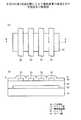
ヒューズ回路を有する従来の半導体装置及びその製造方法について、図11を用いて説明する。図11(a)は従来の半導体装置の構造を示す概略断面図、図11(b)は従来の半導体装置の構造を示す平面図、図11(c)はヒューズ切断後の従来の半導体装置の構造を示す概略断面図である。 A conventional semiconductor device having a fuse circuit and a manufacturing method thereof will be described with reference to FIGS. 11A is a schematic cross-sectional view showing the structure of a conventional semiconductor device, FIG. 11B is a plan view showing the structure of the conventional semiconductor device, and FIG. 11C is a view of the conventional semiconductor device after cutting the fuse. It is a schematic sectional drawing which shows a structure.
下地基板上200には、所定の回路に接続され、回路の切り換えを行うためのヒューズ202が形成されている。ヒューズ202上には、ヒューズ202を覆う層間絶縁膜204が形成されている。層間絶縁膜204上には、層間絶縁膜204を介してヒューズ202に接続された配線層206が形成されている。配線層206上には、パッシベーション膜211が形成され、ヒューズ202上でパッシベーション膜211の一部は除去されている。ヒューズ202は、下地基板200上に所定のピッチPをもって複数形成される(図11(a)、(b))。 On the
このようなヒューズ回路において、ヒューズ202の切断は、ヒューズが形成された領域にレーザ光208を照射し、その吸収エネルギーによってヒューズ202を急激に高温に加熱して溶融爆発(Laser Explosion)することにより行われていた(図11(c))。 In such a fuse circuit, the
ここで、半導体装置を微細化するためにはヒューズ202のピッチPをより狭くすることが必要であるが、ヒューズ202のピッチPは、レーザ光208のスポットサイズ210と、レーザ光208のアライメント精度とによって律則されることとなる。 Here, in order to miniaturize the semiconductor device, it is necessary to make the pitch P of the
レーザ光208のスポットサイズ210は、照射するレーザ光の波長によってその下限が決定されるため、レーザ光の波長を短くすればするほどにスポットサイズ208を小さくすることができる。しかしながら、レーザ光の波長が短すぎるとヒューズ202の形成されていない領域を透過したレーザ光が下地の半導体基板に達して吸収され、そこで加熱溶融爆発してしまう不都合がある。このため、半導体基板がシリコンの場合には、レーザ光の波長は、シリコン基板による吸収が少ない1μm程度、すなわち、スポットサイズにして約1.5〜2.0μmが下限であった。 Since the lower limit of the
一方、アライメント精度は、隣接するヒューズ202の両方を切断する場合に、爆発領域が重なってしまうと下地の半導体基板に損傷が入る不都合を防止するため、及び、隣接するヒューズ202の一方を切断する場合に他方に損傷を与えたり切断してしまうのを防止するために必要であり、通常、約0.5μmがその下限となっている。 On the other hand, the alignment accuracy is such that, when both
したがって、上記従来のヒューズ切断方法では、ヒューズピッチの下限は2.0〜2.5μmであった。 Therefore, in the conventional fuse cutting method, the lower limit of the fuse pitch is 2.0 to 2.5 μm.
ヒューズのピッチPを狭める方法としては、フォトレジストを用いる方法が本出願人の一部において提案されている。 As a method of narrowing the fuse pitch P, a method using a photoresist has been proposed by some of the present applicants.
フォトレジストを用いる方法では、図11(a)に示す半導体装置上にフォトレジスト212を形成し(図12(a))、溶融爆発の生じない十分に低いパワーでレーザ光208を照射してフォトレジスト212を露光し(図12(b))、露光したフォトレジスト212を現像して露光された領域214のフォトレジスト212を除去し(図12(c))、このフォトレジスト212をマスクとしてヒューズ202を通常のエッチングプロセスにて除去する(図12(d))。 In the method using a photoresist, a
この方法によれば、レーザ光208のパワーはフォトレジスト212を感光させるに十分であれば足りるので、ヒューズ202や半導体基板を溶融爆発するほどに高く設定する必要はない。したがって、レーザ光208の波長は容易に短波長化することができるので、レーザ光208のスポットサイズ210もレーザ光の波長に応じていくらでも小さくすることができる。したがって、レーザ光のスポットサイズ210に律則されるヒューズピッチPをも狭めることができる。 According to this method, it is sufficient that the power of the
しかしながら、フォトレジストを用いる方法では、フォトレジストの塗布工程及び現像工程、ヒューズのエッチング工程、フォトレジストの剥離工程を更に設けなければならない。従来、ウェーハプロセス完了後に行う試験工程はウェーハプロセスクリーンルームに比べて清浄度が劣っていても支障がなかったが、エッチング等のプロセスを試験後に行う場合には、試験工程を清浄度の高いクリーンルーム内で行いウェーハに付着したゴミがエッチング装置を汚さないようにするか、ヒューズ切断専用のエッチング装置を配備する必要が生じるため、単なる工程増加以上に製造コストが増加することとなる。 However, in the method using a photoresist, a photoresist coating process and a developing process, a fuse etching process, and a photoresist stripping process must be further provided. Conventionally, the test process performed after the completion of the wafer process has no problem even if the cleanliness is inferior to that of the wafer process clean room. However, if the process such as etching is performed after the test, the test process is performed in a clean room with high cleanliness. In this case, it is necessary to prevent the dust attached to the wafer from fouling the etching apparatus or to provide an etching apparatus dedicated to cutting the fuse, which increases the manufacturing cost more than just increasing the number of processes.
このように、従来のヒューズ切断方法では、半導体装置の高集積化に応じてヒューズピッチを狭め、且つ、製造工程や製造コストの増加を抑えることは困難であった。 As described above, in the conventional fuse cutting method, it is difficult to reduce the fuse pitch in accordance with the high integration of the semiconductor device and to suppress the increase in the manufacturing process and the manufacturing cost.
本発明の目的は、高集積化が容易で製造コストが増加しないヒューズ回路を有する半導体装置の構造及びその製造方法、並びに、このようなヒューズの切断に適したレーザ装置を提供することにある。 An object of the present invention is to provide a structure of a semiconductor device having a fuse circuit that can be easily integrated and does not increase the manufacturing cost, a manufacturing method thereof, and a laser device suitable for cutting such a fuse.
本発明は、レーザアブレーション(Laser Ablation)を用いてヒューズを切断しうる半導体装置及びその製造方法、並びに、このような半導体装置のヒューズを切断するに好適なレーザ装置を提供するのもである。レーザアブレーションとは、高強度のレーザ光を照射し、照射したレーザ光のエネルギーによって物質の結合を解き、被照射物を瞬時に昇華する現象をいうものである。 The present invention also provides a semiconductor device capable of cutting a fuse using laser ablation, a method of manufacturing the same, and a laser device suitable for cutting a fuse of such a semiconductor device. Laser ablation refers to a phenomenon in which high-intensity laser light is irradiated, the bonding of substances is released by the energy of the irradiated laser light, and the irradiated object is instantly sublimated.
レーザ光の吸収による溶融爆発を用いる従来のヒューズ切断方法が、光エネルギーを一旦物質の結合の伸縮等の振動、すなわち、熱エネルギーに変換し、この後に溶融爆発するものであるのに対し、レーザアブレーションは、光エネルギーによって直接物質の結合を解離するものであり、溶融爆発とレーザアブレーションとは全く異なる現象に基づくものである。 Whereas a conventional fuse cutting method using a melt explosion by absorption of laser light converts light energy into vibration such as expansion and contraction of a substance bond, that is, heat energy, and then melts and explodes. Ablation is the dissociation of a substance bond directly by light energy, and is based on a completely different phenomenon between melt explosion and laser ablation.
かかるメカニズムの違いから、レーザアブレーションの場合にはレーザ光を照射した部分のみが消失し、未照射部との境界は極めて奇麗な切断面として残る。一方、従来の溶融爆発では、レーザ照射部近傍まで溶融爆発し、多数の飛散物が生じるとともに、レーザ照射部と未照射部との境界は極めて不鮮明となる。 Due to the difference in mechanism, in the case of laser ablation, only the portion irradiated with the laser beam disappears, and the boundary with the unirradiated portion remains as a very clean cut surface. On the other hand, in the conventional melt explosion, melt explosion occurs in the vicinity of the laser irradiation portion, a large number of scattered matters are generated, and the boundary between the laser irradiation portion and the non-irradiation portion becomes extremely unclear.
このように、レーザアブレーションではレーザ照射部を奇麗に除去することができるが、ほとんど全ての物質を瞬時にして除去してしまうため制御性に欠け、ヒューズのみならず、その下層の半導体基板の一部までもが除去されてしまうという欠点がある。 Thus, laser ablation can cleanly remove the laser irradiation part, but almost all the material is removed instantaneously, so that it lacks controllability, and not only the fuse but also one of the underlying semiconductor substrates. There is a disadvantage that even the part is removed.
上記欠点に鑑み本願発明者等が鋭意検討を行った結果、本願発明者等は、レーザアブレーションにより昇華されにくい材料を見出した。そして、レーザアブレーションにより昇華されにくい所定の材料からなるブロック層をヒューズの下層部に設けておくことにより、このブロック層上でレーザアブレーションを制御性よく停止することができることが初めて明らかとなった。 As a result of intensive studies by the inventors of the present invention in view of the above drawbacks, the inventors of the present application have found a material that is not easily sublimated by laser ablation. It has been clarified for the first time that laser ablation can be stopped with good controllability on the block layer by providing a block layer made of a predetermined material that is not easily sublimated by laser ablation in the lower layer portion of the fuse.
レーザアブレーションによりヒューズを切断する場合であっても、ブロック層によりレーザアブレーションを抑制することができればレーザ光の波長を短くしても従来の溶融爆発のように半導体基板に損傷を与える虞もない。したがって、レーザ光のスポットサイズは、レーザ光の波長に応じていくらでも小さくすることができる。 Even when the fuse is cut by laser ablation, if the laser ablation can be suppressed by the block layer, there is no possibility of damaging the semiconductor substrate as in the case of conventional melt explosion even if the wavelength of the laser beam is shortened. Therefore, the spot size of the laser beam can be reduced as much as the wavelength of the laser beam.
また、互いに隣接する2本のヒューズの両方を切断した場合でも、ブロック層が十分に厚ければ両方のレーザスポットが重なり合っても半導体基板に損傷を与える虞がない。すなわち、ヒューズピッチは、レーザ光の波長を短くすることによっていくらでも縮小することができる。 Further, even when both adjacent two fuses are cut, if the block layer is sufficiently thick, there is no possibility of damaging the semiconductor substrate even if both laser spots overlap. That is, the fuse pitch can be reduced as much as possible by shortening the wavelength of the laser beam.
また、レーザアブレーションでは、ヒューズを切断するために必要とされる装置はレーザ装置のみであり、エッチング装置等を付加する必要はなく、また、製造工程数や製造コストが増加することもない。 In laser ablation, the only device required for cutting the fuse is a laser device, and it is not necessary to add an etching device or the like, and the number of manufacturing steps and manufacturing cost are not increased.
レーザアブレーションを抑制するためのブロック層としては、例えばW(タングステン)膜を用いることができる。 For example, a W (tungsten) film can be used as the block layer for suppressing laser ablation.
すなわち、上記目的は、下地基板上にブロック層を形成するブロック層形成工程と、前記ブロック層上に絶縁膜を形成する絶縁膜形成工程と、前記絶縁膜上にヒューズを形成するヒューズ形成工程と、次いで、前記ヒューズを覆うカバー膜を形成するカバー膜形成工程と、レーザアブレーションにより前記ヒューズを切断するヒューズ切断工程とを有し、前記ヒューズ切断工程では、前記カバー膜と前記ヒューズとを連続して切断するとともに、前記ブロック層でレーザアブレーションを停止することを特徴とする半導体装置の製造方法によって達成される。上記の半導体装置の製造方法によれば、レーザアブレーションによりヒューズを切断しうる半導体装置を製造することができる。また、レーザアブレーションにより切断しうるヒューズは極めて狭いピッチで配置できるので、ヒューズ回路の集積度を向上することができる。That is , the object is to form a block layer forming step for forming a block layer on a base substrate, an insulating film forming step for forming an insulating film on the block layer, and a fuse forming step for forming a fuse on the insulating film.A cover film forming step for forming a cover film covering the fuse; and a fuse cutting step for cutting the fuse by laser ablation. In the fuse cutting step, the cover film and the fuse are continuously connected. with cutting Te, it madereach by the method of manufacturing a semiconductordevice characterized bystopping the laser ablation by the blocking layer. According to the semiconductor device manufacturing method, a semiconductor device capable of cutting a fuse by laser ablation can be manufactured. In addition, since fuses that can be cut by laser ablation can be arranged at an extremely narrow pitch, the degree of integration of the fuse circuit can be improved.
また、レーザアブレーションによりヒューズを切断すれば、製造工程を複雑にせず、且つ、新たな製造装置を配備する必要がないので、製造コストを増加せずにヒューズのピッチを狭めることができる。Further, if cutting the fuse byLes chromatography The ablation, without complicating the manufacturing process, and, since there is no need to deploy a new manufacturing device, it is possible to narrow the pitch of the fuses without increasing the manufacturing cost.
また、レーザアブレーションにより昇華されにくい材料よりなるブロック層をヒューズ下層部に形成しておくことにより、ブロック層で制御性よくレーザアブレーションを停止することができる。Further, by forming a blocking layer made of hard material is sublimated byLes chromatography The ablation fuse lower part, can be stopped with good controllability laser ablation in block layer.
また、上記の半導体装置の製造方法において、前記ヒューズ切断工程では、波長が500nm以下のレーザ光により前記ヒューズを切断することが望ましい。レーザアブレーションでは下地基板のレーザ光の吸収を考慮する必要がないので、基板の吸収帯である1μm以下の波長帯のレーザ光を用いることができる。また、このような短波長レーザ光を用いることによりレーザ光のスポットサイズを縮小することができるので、ヒューズピッチを狭めてヒューズを配置することができる。 In the method for manufacturing a semiconductor device, it is preferable that the fuse is cut with a laser beam having a wavelength of 500 nm or less in the fuse cutting step. In laser ablation, it is not necessary to consider the absorption of the laser beam of the base substrate, and therefore, a laser beam having a wavelength band of 1 μm or less that is an absorption band of the substrate can be used. Further, since the spot size of the laser beam can be reduced by using such a short wavelength laser beam, the fuse pitch can be reduced and the fuse can be arranged.
また、上記の半導体装置の製造方法において、前記レーザ光は、Nd:YAGレーザの第3高調波又はNd:YLFレーザの第3高調波であることが望ましい。 In the method for manufacturing a semiconductor device, the laser beam is preferably a third harmonic of an Nd: YAG laser or a third harmonic of an Nd: YLF laser.
また、上記の半導体装置の製造方法において、前記ヒューズ形成工程の後に、前記ヒューズ上を覆うカバー膜を形成するカバー膜形成工程を更に有することが望ましい。レーザアブレーションでは、上層部から順次昇華していくので、ヒューズ上にカバー膜が形成されている場合であってもカバー膜上からヒューズを切断することができる。 The semiconductor device manufacturing method preferably further includes a cover film forming step of forming a cover film covering the fuse after the fuse forming step. In laser ablation, since sublimation is sequentially performed from the upper layer portion, the fuse can be cut from the cover film even when the cover film is formed on the fuse.
また、上記の半導体装置の製造方法において、前記カバー膜形成工程の後に、組立の際のストレスを緩和するためのポリイミド膜を形成するポリイミド膜形成工程を更に有することが望ましい。また、カバー膜上にポリイミド膜が形成されている場合であっても、同様に、ポリイミド膜上からヒューズを切断することができる。 The semiconductor device manufacturing method preferably further includes a polyimide film forming step of forming a polyimide film for relieving stress during assembly after the cover film forming step. Further, even when a polyimide film is formed on the cover film, the fuse can be similarly cut from the polyimide film.
また、上記の半導体装置の製造方法において、前記ブロック層形成工程では、タングステン膜を含む前記ブロック層を形成することが望ましい。 In the method for manufacturing a semiconductor device, it is preferable that the block layer including a tungsten film is formed in the block layer forming step.
また、上記の半導体装置の製造方法において、前記ヒューズ形成工程では、アルミ膜又はアルミ合金膜を含む前記ヒューズを形成するようにしてもよい。In the semiconductor device manufacturing method, the fuse including the aluminum film or the aluminum alloy film may be formed in the fuse forming step.
以上の通り、本発明によれば、下地基板上に形成されたブロック層と、ブロック層上に形成された絶縁膜と、絶縁膜上に形成されたヒューズとにより半導体装置を構成するので、下地基板に損傷を与えることなく制御性よくレーザアブレーションによりヒューズを切断することができる。また、レーザアブレーションにより切断しうるヒューズは極めて狭いピッチで配置できるので、ヒューズ回路の集積度を向上することができる。 As described above, according to the present invention, the semiconductor device is configured by the block layer formed on the base substrate, the insulating film formed on the block layer, and the fuse formed on the insulating film. The fuse can be cut by laser ablation with good controllability without damaging the substrate. In addition, since fuses that can be cut by laser ablation can be arranged at an extremely narrow pitch, the degree of integration of the fuse circuit can be improved.
また、複数のメモリセルが形成されたメモリセル領域と、不良メモリセルを冗長メモリセルに切り換えるヒューズ回路が形成されたヒューズ回路領域とを有する半導体装置であって、ヒューズ回路領域に形成されたブロック層と、ブロック層上に形成された絶縁膜と、絶縁膜上に形成され、メモリセルを構成する導電層又はメモリセル領域に形成された配線層と同一の導電層よりなるヒューズとを有することを特徴とする半導体装置によっても達成される。このように半導体装置を構成することにより、レーザアブレーションにより制御性よく切断しうるヒューズをメモリデバイスにおける冗長回路への切り換え回路に適用することができる。また、レーザアブレーションにより切断しうるヒューズは極めて狭いピッチで配置できるので、メモリデバイスの集積度を向上することができる。 Also, a semiconductor device having a memory cell region in which a plurality of memory cells are formed and a fuse circuit region in which a fuse circuit for switching a defective memory cell to a redundant memory cell is formed, the block formed in the fuse circuit region A layer, an insulating film formed on the block layer, and a fuse formed on the insulating film and made of the same conductive layer as the conductive layer constituting the memory cell or the wiring layer formed in the memory cell region This is also achieved by a semiconductor device characterized by the above. By configuring the semiconductor device in this manner, a fuse that can be cut with good controllability by laser ablation can be applied to a switching circuit to a redundant circuit in a memory device. Further, since fuses that can be cut by laser ablation can be arranged at an extremely narrow pitch, the degree of integration of memory devices can be improved.
また、下地基板上にブロック層を形成するブロック層形成工程と、ブロック層上に絶縁膜を形成する絶縁膜形成工程と、絶縁膜上にヒューズを形成するヒューズ形成工程とにより半導体装置を製造することにより、レーザアブレーションにより切断しうるヒューズを有する半導体装置を製造することができる。また、レーザアブレーションにより切断しうるヒューズは極めて狭いピッチで配置できるので、ヒューズ回路の集積度を向上することができるまた、レーザアブレーションによりヒューズを切断すれば、製造工程を複雑にせず、且つ、新たな製造装置を配備する必要がないので、製造コストを増加せずにヒューズのピッチを狭めることができる。 Further, a semiconductor device is manufactured by a block layer forming process for forming a block layer on the base substrate, an insulating film forming process for forming an insulating film on the block layer, and a fuse forming process for forming a fuse on the insulating film. Thus, a semiconductor device having a fuse that can be cut by laser ablation can be manufactured. In addition, since fuses that can be cut by laser ablation can be arranged at an extremely narrow pitch, the integration of the fuse circuit can be improved. Also, if the fuses are cut by laser ablation, the manufacturing process is not complicated and a new one can be obtained. Since it is not necessary to provide a simple manufacturing apparatus, the pitch of the fuse can be reduced without increasing the manufacturing cost.
また、下地基板上に形成されたブロック層と、ブロック層上に形成された絶縁膜と、絶縁膜上に形成されたヒューズとを有する半導体装置のヒューズをレーザアブレーションにより切断するためのレーザ装置であって、500nm以下の発振波長を有し、ヒューズをレーザアブレーションにより切断するために十分なエネルギー密度を有するレーザ光を発振するレーザ共振器と、レーザ共振器により出力されたレーザ光を所定のスポットサイズに集光するレンズ機構と、レーザ共振器により出力されたレーザ光を半導体装置の所定の位置に照射するための位置合わせ機構とによりレーザ装置を構成することにより、ウェーハの任意の位置にレーザ光を照射し、レーザアブレーションによりヒューズを切断することができる。 A laser device for cutting a fuse of a semiconductor device having a block layer formed on a base substrate, an insulating film formed on the block layer, and a fuse formed on the insulating film by laser ablation. A laser resonator that oscillates a laser beam having an oscillation wavelength of 500 nm or less and a sufficient energy density for cutting the fuse by laser ablation, and a laser beam output from the laser resonator at a predetermined spot A laser device is configured by a lens mechanism that focuses light on a size and an alignment mechanism that irradiates a laser beam output from a laser resonator to a predetermined position of the semiconductor device, so that a laser can be applied to an arbitrary position on the wafer. Light can be irradiated and the fuse can be cut by laser ablation.
[第1実施形態]
本発明の第1実施形態による半導体装置及びその製造方法について図1乃至図4を用いて説明する。[First Embodiment]
The semiconductor device and the manufacturing method thereof according to the first embodiment of the present invention will be described with reference to FIGS.
図1は本実施形態による半導体装置の構造を示す平面図及び断面図、図2は本実施形態による半導体装置の製造方法を示す工程図、図3及び図4は本実施形態による半導体装置の製造方法を示す工程断面図である。 FIG. 1 is a plan view and a cross-sectional view showing the structure of the semiconductor device according to the present embodiment, FIG. 2 is a process diagram showing the method for manufacturing the semiconductor device according to the present embodiment, and FIGS. It is process sectional drawing which shows a method.
はじめに、本実施形態による半導体装置の構造について図1を用いて説明する。図1(a)は本実施形態による半導体装置の構造を示す平面図、図1(b)は図1(a)のX−X′線断面図である。 First, the structure of the semiconductor device according to the present embodiment will be explained with reference to FIG. FIG. 1A is a plan view showing the structure of the semiconductor device according to the present embodiment, and FIG. 1B is a sectional view taken along line XX ′ in FIG.
下地基板10上には、レーザアブレーションを抑制するブロック層12が形成されている。下地基板10及びブロック層12上には、層間絶縁膜14が形成されている。層間絶縁膜14上には、例えばアルミや多結晶シリコンなどの導電膜よりなるヒューズ22が複数形成されている。ヒューズ22上には、カバー膜30が形成されている。 A
このように、本実施形態による半導体装置では、ヒューズ22が形成された領域の下層に、レーザアブレーションを抑制するブロック層12が形成されていることに特徴がある。このようなブロック層12を設けることにより、制御性に欠けるレーザアブレーションを用いてヒューズ22を切断する場合にもブロック層12で制御性よくレーザアブレーションを停止することができる。 Thus, the semiconductor device according to the present embodiment is characterized in that the
ブロック層12としては、レーザアブレーションにより昇華されにくい材料を適用することが望ましく、具体的には、W(タングステン)膜や、W/TiN/Tiなどの積層膜を用いることができる。これらの膜や積層膜は、従来より半導体装置の製造に広く用いられているものであり、プロセスの整合性にも優れている。 As the
また、特別にブロック作用を有しなくても、ヒューズ22と半導体基板間に配置される膜が厚ければ厚いほどよいので、半導体装置に用いられる全ての層をヒューズ22下部に配置してもブロック層12としての機能を発揮できる。 Even if it does not have a special blocking action, the thicker the film disposed between the
ヒューズ22としては、ブロック層12に比べて十分にレーザアブレーションされやすい材料であれば如何なる材料であっても適用することができる。実際に半導体装置に使用されている材料としては、例えば、多結晶シリコン、金属シリサイド、Al、Al−Si−CuやAl−Cu−TiなどのAl合金、Ti、TiN、又はこれらの積層膜を用いることができる。 As the
ヒューズ22のピッチは、レーザ光のスポットサイズと位置合わせ余裕とにより律則される。レーザ光の最小スポットサイズは、概略、レーザ光の波長の約2倍と見積もることができるので、例えばレーザ光の波長を0.355μm、位置合わせ余裕を0.5μmとすると、ヒューズ22のピッチは約1.2μmとなる。したがって、従来の半導体装置と比較して、ヒューズ22のピッチを極めて狭くすることができる。 The pitch of the
また、2回のレーザアブレーションに耐えうる膜厚を有するブロック層を設けておけば、隣接するヒューズを切断するためのレーザ光のスポットが重なり合っても下地に損傷を与える虞がないので、位置合わせ余裕を確保する必要はない。したがって、ヒューズピッチは更に狭めることができる。 In addition, if a block layer having a thickness that can withstand two laser ablation steps is provided, there is no possibility of damaging the substrate even if the laser beam spots for cutting adjacent fuses overlap. There is no need to secure a margin. Therefore, the fuse pitch can be further reduced.
また、レーザアブレーションでは下地基板による吸収を考慮する必要がないので、レーザ光の波長を短くすることによりヒューズピッチを更に狭めることができる。したがって、半導体装置の微細化に極めて有効である。 In laser ablation, it is not necessary to consider the absorption by the base substrate, so that the fuse pitch can be further narrowed by shortening the wavelength of the laser beam. Therefore, it is extremely effective for miniaturization of a semiconductor device.
このように、本実施形態によれば、ヒューズの下層部にレーザアブレーションにより昇華されにくい材料からなるブロック層を設けるので、レーザアブレーションにより制御性よくヒューズの切断をしうる半導体装置を構成することができる。 As described above, according to the present embodiment, since the block layer made of a material that is not easily sublimated by laser ablation is provided in the lower layer portion of the fuse, a semiconductor device capable of cutting the fuse with controllability by laser ablation can be configured. it can.
また、レーザアブレーションでは、レーザ光の波長を短くしても下地基板に影響を与えないので、レーザ光のスポットサイズをレーザ光の波長に応じて極めて小さくすることができる。これにより、ヒューズピッチを狭めることができるので、半導体装置の集積度を向上することができる。 In laser ablation, even if the wavelength of the laser beam is shortened, the underlying substrate is not affected. Therefore, the spot size of the laser beam can be made extremely small according to the wavelength of the laser beam. Thereby, since the fuse pitch can be narrowed, the degree of integration of the semiconductor device can be improved.
次に、本実施形態による半導体装置の製造方法について図2乃至図4を用いて説明する。 Next, the method for fabricating the semiconductor device according to the present embodiment will be explained with reference to FIGS.
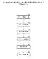
本実施形態による半導体装置の製造方法は、図2に示すように、下地基板上にレーザアブレーションを抑制するブロック層を形成する工程(ステップS11)と、ブロック層上に絶縁膜を介してヒューズを形成する工程(ステップS12)と、ヒューズ上を覆うカバー膜を形成する工程(ステップS13)と、回路の動作試験を行う試験工程(ステップS14)と、レーザアブレーションによりヒューズを切断する工程(ステップS15)とにより半導体装置を製造することに特徴がある。 As shown in FIG. 2, the method of manufacturing the semiconductor device according to the present embodiment includes a step of forming a block layer for suppressing laser ablation on a base substrate (step S11), and a fuse on the block layer via an insulating film. Step of forming (Step S12), Step of forming a cover film covering the fuse (Step S13), Test step of performing circuit operation test (Step S14), Step of cutting the fuse by laser ablation (Step S15) ) Is characterized by manufacturing a semiconductor device.
以下、具体的な構造を例に本実施形態による半導体装置の製造方法を詳細に説明する。 Hereinafter, the method for fabricating the semiconductor device according to the present embodiment will be described in detail by taking a specific structure as an example.
まず、所定の素子が形成された下地基板10上に、レーザアブレーションを抑制するためのブロック層12を形成する(ステップS11)。例えば、下地基板10上にCVD法により膜厚約350nmのW膜を堆積して所定の形状にパターニングし、ブロック層12とする。 First, the
次いで、ブロック層12を覆う層間絶縁膜14を形成する。例えば、CVD法により膜厚約1μmのシリコン酸化膜を堆積し、層間絶縁膜14とする(図3(b))。 Next, an
続いて、層間絶縁膜14上に、ヒューズとなる導電膜を堆積する。例えば、スパッタ法により、膜厚約100nmのTiN膜16と、膜厚約1μmのAl−Cu−Ti膜18と、膜厚約50nmのTiN膜20とを堆積する。 Subsequently, a conductive film to be a fuse is deposited on the
この後、通常のリソグラフィー技術及びエッチング技術により、TiN膜20/Al−Cu−Ti膜18/TiN膜16よりなる積層膜をパターニングし、ブロック層12の上部に、この積層膜よりなるヒューズ22を形成する(ステップS12、図3(c))。例えば、ブロック層12上に、幅約2μmのヒューズ22を2μmピッチで複数配置する。 Thereafter, the laminated film made of the
次いで、ヒューズ22が形成された基板上にカバー膜30を形成する(ステップS13)。例えば、CVD法により膜厚約100nmのSiON膜24を堆積し、次いで膜厚約1μmのSOG膜26を塗布して表面を平坦化し、続いてCVD法により膜厚約1μmのSiN膜28を堆積し、SiON膜24と、SOG膜26と、SiN膜28とからなるカバー膜30を形成する(図4(a))。 Next, the
続いて、通常のリソグラフィー技術及びエッチング技術により、ボンディングパッド(図示せず)を露出するための開口部をカバー膜に形成する。 Subsequently, an opening for exposing a bonding pad (not shown) is formed in the cover film by a normal lithography technique and an etching technique.
溶融爆発によりヒューズを切断する従来の半導体装置の製造方法では、溶融爆発を起こすためにカバー膜を除去し、或いは薄くする必要があり、通常、ボンディングパッドの開口と同時にヒューズ窓を形成するためのエッチングを行っていた。しかしながら、レーザアブレーションを用いる本実施形態による半導体装置の製造方法では、上層の膜から順次昇華していくためカバー膜30にヒューズ窓を形成する必要はない。したがって、カバー膜30のパターニング工程では、100μm単位の大きなパッド開口部のみを形成すれば十分であり微細なヒューズ窓を形成する必要はないので、リソグラフィー工程を簡略にすることができる。このことは、従来のようにヒューズ窓を形成してはいけないことを意味するものではない。ヒューズ窓を形成すれば、ヒューズ上の膜が少なくなるためレーザアブレーションのトータルパワーを減少でき、また、スループットの増加及びより高精度のレーザアブレーション制御も可能となるなどのメリットを得ることができる。 In the conventional method of manufacturing a semiconductor device in which a fuse is cut by a melt explosion, it is necessary to remove or thin the cover film in order to cause a melt explosion. Usually, a fuse window is formed simultaneously with the opening of a bonding pad. Etching was performed. However, in the manufacturing method of the semiconductor device according to the present embodiment using laser ablation, it is not necessary to form a fuse window in the
この後、所定の回路試験を行い不良メモリセル等を特定し、冗長メモリセルと切り換えるために切断すべきヒューズを特定する(ステップS14)。この際、切断すべきヒューズ22のウェーハ上における位置座標を予め記憶しておき、ヒューズ切断の際に用いる。 Thereafter, a predetermined circuit test is performed to identify a defective memory cell and the like, and a fuse to be cut for switching to a redundant memory cell is identified (step S14). At this time, the position coordinates of the
次いで、レーザアブレーション法を用い、回路試験により特定されたヒューズ22を切断する(ステップS15、図4(b))。なお、上述の構造では、発振波長355nm、パルス幅40nsec、パワー100μJ、スポットサイズ5μmの条件により、ブロック層12でレーザアブレーションを停止しつつヒューズ22を切断することができた。なお、レーザ光のスポットサイズは、1.5μm程度のものを使用することもでき、更には波長の2倍程度まで縮小可能である。 Next, the
この後、必要に応じて再度回路試験を行い、良品の組立を行う。 After this, the circuit test is performed again as necessary to assemble non-defective products.
このように、本実施形態によれば、レーザアブレーションを用いてヒューズ22を切断するので、カバー膜30にヒューズ窓を設けることなくヒューズ22を切断することができる。これにより、カバー膜30のパターニングの際のリソグラフィー工程を簡略にすることができる。また、ヒューズ22の切断にフォトレジストやエッチング装置を用いる必要がないので、ヒューズ切断専用のエッチング装置などを新たに配備する必要もない。 Thus, according to this embodiment, since the
また、レーザアブレーションではレーザの波長を独立して短波長化することができるので、レーザのスポットサイズを極めて小さくすることができる。これにより、ヒューズ回路を構成する領域の専有面積を大幅に縮小することができるので、半導体装置の集積度を向上することができる。 In laser ablation, the laser wavelength can be shortened independently, so that the laser spot size can be made extremely small. As a result, the area occupied by the region constituting the fuse circuit can be greatly reduced, so that the degree of integration of the semiconductor device can be improved.
なお、半導体チップをセラミックパッケージに封入する際のチップとセラミックとの間の熱膨張差などによる影響を抑えるため、カバー膜30上に緩衝材としてポリイミド膜を形成する場合がある。このような場合にも、本実施形態による半導体装置の製造方法は有効である。すなわち、レーザアブレーションを用いる本実施形態の半導体装置の製造方法では、対象物の表面側から順次昇華していくので、カバー膜上にポリイミド膜が形成されている場合であってもポリイミド膜上からヒューズを切断することができる。 Note that a polyimide film may be formed on the
例えば、図5に示すように、下地基板上にブロック層を形成し(ステップS21)、ブロック層上に層間絶縁膜を介してヒューズを形成し(ステップS22)、ヒューズ上を覆うカバー膜を形成し(ステップS23)、カバー膜を覆うポリイミド膜を形成し(ステップS24)、その後、所定の動作試験を行い(ステップS25)、レーザアブレーションによりヒューズを切断(ステップS25)することができる。 For example, as shown in FIG. 5, a block layer is formed on the base substrate (step S21), a fuse is formed on the block layer via an interlayer insulating film (step S22), and a cover film covering the fuse is formed. Then, a polyimide film covering the cover film is formed (step S24), and then a predetermined operation test is performed (step S25), and the fuse can be cut by laser ablation (step S25).
また、上記実施形態ではカバー膜の形成後に動作試験を行っているが、少なくとも最終配線層が形成されていれば動作試験を行うことができる。また、ヒューズの切断は、動作試験の後であれば行うことができる。したがって、例えば図6に示すように、下地基板上にブロック層を形成する工程(ステップS31)と、ブロック層上に絶縁膜を介してヒューズを形成する工程(ステップS32)と、ヒューズ上を覆うカバー膜を形成する工程(ステップS33)と、カバー膜を覆うポリイミド膜を形成する工程(ステップS34)とを有する半導体装置の製造方法において、動作試験工程(ステップS35)は、カバー膜形成工程の前に行ってもよいし、ポリイミド膜形成工程の前に行ってもよいし、ポリイミド膜形成工程の後に行ってもよい。また、ヒューズ切断工程(ステップS36)は、動作試験工程(ステップS35)の後であれば、カバー膜形成工程の前に行ってもよいし、ポリイミド膜形成工程の前に行ってもよいし、ポリイミド膜形成工程の後に行ってもよい。 In the above embodiment, the operation test is performed after the cover film is formed. However, the operation test can be performed if at least the final wiring layer is formed. Also, the fuse can be cut after the operation test. Therefore, for example, as shown in FIG. 6, a step of forming a block layer on the base substrate (step S31), a step of forming a fuse on the block layer via an insulating film (step S32), and covering the fuse In the method for manufacturing a semiconductor device including the step of forming a cover film (step S33) and the step of forming a polyimide film covering the cover film (step S34), the operation test step (step S35) is a cover film forming step. It may be performed before, may be performed before the polyimide film forming step, or may be performed after the polyimide film forming step. Further, the fuse cutting step (step S36) may be performed before the cover film forming step or before the polyimide film forming step as long as it is after the operation test step (step S35). You may perform after a polyimide film formation process.
[第2実施形態]
本発明の第2実施形態による半導体装置の構造について図7を用いて説明する。[Second Embodiment]
The structure of the semiconductor device according to the second embodiment of the present invention will be explained with reference to FIG.
図7は本実施形態による半導体装置の構造を示す概略断面図である。 FIG. 7 is a schematic sectional view showing the structure of the semiconductor device according to the present embodiment.
本実施形態では、第1実施形態による半導体装置及びその製造方法をDRAMに適用した場合の一例について説明する。DRAMでは、メモリセルを指定するアドレス回路の切り換えにヒューズ回路を使用し、ヒューズ回路の所定のヒューズを切断することにより不良メモリセルのアドレスを冗長メモリセルに切り換えることが行われている。このようにDRAMを構成することにより、一部のメモリセルが不良である場合にも、このメモリセルを冗長メモリセルに切り換えることで装置全体が不良となることから救済することができる。 In the present embodiment, an example in which the semiconductor device and the manufacturing method thereof according to the first embodiment are applied to a DRAM will be described. In a DRAM, a fuse circuit is used to switch an address circuit that designates a memory cell, and an address of a defective memory cell is switched to a redundant memory cell by cutting a predetermined fuse of the fuse circuit. By configuring the DRAM in this way, even when some of the memory cells are defective, switching the memory cells to redundant memory cells can be remedied because the entire device becomes defective.
シリコン基板40上には、複数のメモリセルが形成されたメモリセル領域42と、メモリセルを駆動するための周辺回路が形成された周辺回路領域44と、不良メモリセルを冗長メモリセルに切り換えるためのヒューズ回路が形成されたヒューズ回路領域46とが設けられている。 On the
シリコン基板40には、素子領域を画定するための素子分離膜48が形成されている。メモリセル領域42のシリコン基板40には、ゲート電極50とソース/ドレイン拡散層52、54とからなる転送トランジスタが形成されている。ソース/ドレイン拡散層52には、ビット線56が接続されている。ソース/ドレイン拡散層54には、フィン型の蓄積電極58が接続されている。蓄積電極58は、誘電体膜を介して対向電極60により覆われており、蓄積電極58、誘電体膜、対向電極60とからなるキャパシタが形成されている。こうして、メモリセル領域42には、転送トランジスタ及びキャパシタとからなるメモリセルが複数形成されている。なお、図7に示すメモリセルの構造については、例えば同一出願人による特公平8−28476号公報に詳述されている。周辺回路領域44には、周辺回路を構成する複数の周辺トランジスタ(図示せず)が形成されている。メモリセル及び周辺トランジスタが形成されたシリコン基板40上には、層間絶縁膜62が形成されている。ヒューズ領域46の層間絶縁膜62上には、W膜よりなるレーザアブレーションを抑制するためのブロック層64が形成されている。ブロック層64が形成された層間絶縁膜52上には、層間絶縁膜66が形成されている。層間絶縁膜66上には、同一のAl合金層により形成された裏打ちワード線68と、周辺トランジスタを相互接続して周辺回路を構成するための配線層70とが形成されている。裏打ちワード線68、配線層70が形成された層間絶縁膜66上には、層間絶縁膜72が形成されている。層間絶縁膜72上には、同一のAl合金層により形成された配線層74とヒューズ76とが形成されている。配線層74及びヒューズ76が形成された層間絶縁膜72上には、カバー膜78が形成されている。 An
このように、本実施形態による半導体装置は、第1実施形態による半導体装置を、DRAMにおける冗長回路への切り換えを行うヒューズ回路に適用していることに特徴がある。すなわち、ヒューズ回路のヒューズをDRAMを構成するための第2金属配線層により構成し、ヒューズ76の下層にレーザアブレーションを抑制するブロック層64を形成している。このように半導体装置を構成することにより、レーザアブレーションにより制御性よくヒューズを切断することができる。 As described above, the semiconductor device according to the present embodiment is characterized in that the semiconductor device according to the first embodiment is applied to a fuse circuit for switching to a redundant circuit in a DRAM. That is, the fuse of the fuse circuit is constituted by the second metal wiring layer for constituting the DRAM, and the
なお、ヒューズの切断は、第1実施形態による半導体装置の製造方法と同様に行うことができる。 The fuse can be cut in the same manner as in the semiconductor device manufacturing method according to the first embodiment.
このように、本実施形態によれば、DRAMにおける冗長回路への切り換えのためのヒューズ回路として、ヒューズ76の下層にレーザアブレーションにより昇華されにくい材料よりなるブロック層64を有するヒューズ回路を適用するので、レーザアブレーションにより制御性よくヒューズを切断しうる半導体装置を構成することができる。 Thus, according to the present embodiment, the fuse circuit having the
また、レーザアブレーションではレーザ光の波長を短くしても下地基板に影響を与えないので、レーザ光のスポットサイズをレーザ光の波長に応じて極めて小さくすることができる。これにより、ヒューズピッチを狭めることができるので、DRAMの集積度を向上することができる。 In laser ablation, even if the wavelength of the laser beam is shortened, the underlying substrate is not affected. Therefore, the spot size of the laser beam can be made extremely small according to the wavelength of the laser beam. Thereby, since the fuse pitch can be narrowed, the integration degree of DRAM can be improved.
なお、上記実施形態では、ヒューズ76を構成する配線層として第2金属配線層を用いたが、必ずしも第2金属配線層である必要はない。すなわち、レーザアブレーションでは被対象物の上層部から順次昇華していくので、ヒューズを覆う上層の膜厚には影響されない。したがって、ヒューズ76を構成する配線層を必ずしも最上層の配線層とする必要はなく、例えば図8に示すように、第1金属配線層によりヒューズ76を構成することもできる。また、3層以上の金属配線層を有する場合にも、何れの配線層でヒューズ76を構成してもよい。 In the above embodiment, the second metal wiring layer is used as the wiring layer constituting the
また、レーザアブレーションにより昇華されにくい材料よりなるブロック層64をヒューズ76の下層側に配置すれば、金属配線層のみならず、その他の導電層によりヒューズ76を構成してもよい。例えば、図9に示すように、対向電極60と同一導電層によりヒューズ76を構成し、その下層にブロック層64を形成することができる。ブロック層64としては、新たに挿入した膜を適用してもよいし、ヒューズ76の下層側に位置する導電層、例えば、蓄積電極58、ビット線56、ワード線50と同一導電層により構成してもよい。 In addition, if the
同様に、蓄積電極、或いは、ビット線と同一導電層によりヒューズを構成することもできる。 Similarly, a fuse can be formed of the same conductive layer as the storage electrode or the bit line.
また、上記実施形態では、フィン型のキャパシタを有するDRAMに第1実施形態のヒューズ回路を適用した場合について説明したが、フィン型のキャパシタを有するDRAMに限らず、種々の構造のDRAMに適用することができる。また、DRAMのみならず、SRAMその他のメモリ素子にも適用することができる。 In the above embodiment, the case where the fuse circuit of the first embodiment is applied to a DRAM having a fin-type capacitor has been described. However, the present invention is not limited to a DRAM having a fin-type capacitor, and is applicable to DRAMs having various structures. be able to. Further, the present invention can be applied not only to DRAM but also to SRAM and other memory elements.
[第3実施形態]
本発明の第3実施形態によるレーザ装置について図10を用いて説明する。[Third Embodiment]
A laser apparatus according to a third embodiment of the present invention will be described with reference to FIG.
図10は本実施形態によるレーザ装置の構造を示す概略図である。 FIG. 10 is a schematic view showing the structure of the laser apparatus according to the present embodiment.
本実施形態では、第2実施形態による半導体装置の製造方法に適用しうるレーザ装置について説明する。 In the present embodiment, a laser device that can be applied to the semiconductor device manufacturing method according to the second embodiment will be described.
本実施形態によるレーザ装置は、主として、レーザ光を発振するためのレーザ共振器100と、レーザ共振器のレーザ光源を光ポンピングするためのレーザダイオード120と、レーザ共振器100から発せられたレーザ光を所定のスポットサイズに集光するレンズ機構118と、レーザ共振器100から発せられたレーザ光をステージ140上に搭載されたウェーハ142の所定の位置に照射するビーム位置合わせ機構130とにより構成される。 The laser apparatus according to this embodiment mainly includes a
レーザダイオード120から発せられた光122は、レンズ機構124を通してレーザ共振器100に入射するようになっており、レーザ共振器100のレーザ光源を光ポンピングする。 The light 122 emitted from the
レーザ共振器100は、レーザ光源102と、レーザ光源102を挟んで配置された誘導放出を持続するための2枚のミラー104、106と、レーザ光の周波数を変換し或いは調整するための制御機構108、110、112と、光共振器のQを急速に変化するためのQスイッチ114とがレーザ光の光軸116上に沿って配置されてなる。レーザ光源102としては、例えば、発振波長442nmのHe−Cd気体レーザ、第3高調波の発振波長が355nmであるNd:YAG固体レーザ、第3高調波の発振波長が349nmであるNd:YLF固体レーザを用いることができる。ミラー106は、ほぼ100%の反射率でレーザ光を反射することが望ましく、ミラー104は、一部のレーザ光が透過されるように構成され、ミラー104を透過した光は出力光として用いられる。制御機構108、110、112は、レーザ光をそのまま用いることができる場合には必ずしも必要ないが、制御機構108、110、112を設けることにより、レーザ光の波長を、光パラメトリック発振(optical parametric oscillation)や2倍、3倍、4倍の非線形周波数変換を用いて所望の発振波長に変換することができる。ミラー104を透過したレーザ光は、レンズ機構118を介してビーム位置合わせ機構130に入射される。 The
ビーム位置合わせ機構130は、複数の反射板132、134、136、138により構成されており、反射板132、134、136、138を適宜制御することによりレーザ共振器100から出力されたレーザ光をウェーハ140上の所定の位置に照射できるようになっている。ビーム位置合わせ機構130及びウェーハ140に照射されるレーザ光は、レンズ機構144により所望のスポットサイズに成型される。 The
レーザ共振器100、レーザダイオード120、ビーム位置合わせ機構130、ステージ140は、レーザ制御装置150によって同期制御され、所定のレーザ発振条件で発せられたレーザ光を、所定のタイミングで、ウェーハ142上の所定の位置に照射できるようになっている。なお、ウェーハ142上における座標情報は、予めチップ146の動作試験を行い切断すべきヒューズの座標をデータ化しておき、レーザ照射の際にレーザ制御装置に与えればよい。 The
このようにしてレーザ装置を構成することにより、ウェーハの任意の位置にレーザ光を照射し、レーザアブレーションによりヒューズを切断することができる。 By configuring the laser device in this manner, it is possible to irradiate laser light to an arbitrary position on the wafer and cut the fuse by laser ablation.
10…下地基板
12…ブロック層
14…層間絶縁膜
16…TiN膜
18…Al−Cu−Ti膜
20…TiN膜
22…ヒューズ
24…SiON膜
26…SOG膜
28…SiN膜
30…カバー膜
40…シリコン基板
42…メモリセル領域
44…周辺回路領域
46…ヒューズ回路領域
48…素子分離膜
50…ゲート電極
52、54…ソース/ドレイン拡散層
56…ビット線
58…蓄積電極
60…対向電極
62、66、72、78…層間絶縁膜
64…ブロック層
68…裏打ちワード線
70、74…配線層
76…ヒューズ
100…レーザ共振器
102…レーザ光源
104、106…ミラー
108、110、112…制御機構
114…Qスイッチ
116…光軸
118、124、144…レンズ機構
120…レーザダイオード
122…光
130…ビーム位置合わせ機構
132、134、136、138…反射板
140…ステージ
142…ウェーハ
146…チップ
200…下地基板
202…ヒューズ
204…層間絶縁膜
206…配線層
208…レーザ光
210…スポットサイズ
211…パッシベーション膜
212…フォトレジスト
214…露光された領域のフォトレジスト
DESCRIPTION OF
Claims (7)
Translated fromJapanese前記ブロック層上に絶縁膜を形成する絶縁膜形成工程と、
前記絶縁膜上にヒューズを形成するヒューズ形成工程と、
次いで、前記ヒューズを覆うカバー膜を形成するカバー膜形成工程と、
レーザアブレーションにより前記ヒューズを切断するヒューズ切断工程とを有し、
前記ヒューズ切断工程では、前記カバー膜と前記ヒューズとを連続して切断するとともに、前記ブロック層でレーザアブレーションを停止する
ことを特徴とする半導体装置の製造方法。A block layer forming step of forming a block layer on the base substrate;
An insulating film forming step of forming an insulating film on the block layer;
A fuse forming a fuse on the insulatingfilm,
Next, a cover film forming step for forming a cover film covering the fuse,
A fuse cutting step for cutting the fuse by laser ablation,
In the fuse cutting step, the cover film and the fuse are continuously cut, and laser ablation is stopped at the block layer .
前記ヒューズ切断工程では、波長が500nm以下のレーザ光により前記ヒューズを切断する
ことを特徴とする半導体装置の製造方法。In the manufacturing method of the semiconductor device according to claim1 ,
In the fuse cutting step, the fuse is cut by a laser beam having a wavelength of 500 nm or less.
前記レーザ光は、Nd:YAGレーザの第3高調波又はNd:YLFレーザの第3高調波である
ことを特徴とする半導体装置の製造方法。The method of manufacturing a semiconductor device according to claim2 .
The method of manufacturing a semiconductor device, wherein the laser beam is a third harmonic of an Nd: YAG laser or a third harmonic of an Nd: YLF laser.
前記ヒューズ形成工程の後に、前記ヒューズ上を覆うカバー膜を形成するカバー膜形成工程を更に有する
ことを特徴とする半導体装置の製造方法。In the manufacturing method of the semiconductor device according to anyone of claims1 to3 ,
A method for manufacturing a semiconductor device, further comprising a cover film forming step of forming a cover film covering the fuse after the fuse forming step.
前記カバー膜形成工程の後に、組立の際のストレスを緩和するためのポリイミド膜を形成するポリイミド膜形成工程を更に有する
ことを特徴とする半導体装置の製造方法。In the manufacturing method of the semiconductor device according to claim4 ,
A method of manufacturing a semiconductor device, further comprising a polyimide film forming step of forming a polyimide film for relieving stress during assembly after the cover film forming step.
前記ブロック層形成工程では、タングステン膜を含む前記ブロック層を形成する
ことを特徴とする半導体装置の製造方法。In the manufacturing method of the semiconductor device according to anyone of claims1 to5 ,
In the block layer forming step, the block layer including a tungsten film is formed. A method for manufacturing a semiconductor device, comprising:
前記ヒューズ形成工程では、アルミ膜又はアルミ合金膜を含む前記ヒューズを形成するIn the fuse forming step, the fuse including an aluminum film or an aluminum alloy film is formed.
ことを特徴とする半導体装置の製造方法。A method for manufacturing a semiconductor device.
Priority Applications (1)
| Application Number | Priority Date | Filing Date | Title |
|---|---|---|---|
| JP2009230699AJP4970518B2 (en) | 2009-10-02 | 2009-10-02 | Manufacturing method of semiconductor device |
Applications Claiming Priority (1)
| Application Number | Priority Date | Filing Date | Title |
|---|---|---|---|
| JP2009230699AJP4970518B2 (en) | 2009-10-02 | 2009-10-02 | Manufacturing method of semiconductor device |
Related Parent Applications (1)
| Application Number | Title | Priority Date | Filing Date |
|---|---|---|---|
| JP10151309ADivisionJPH11345880A (en) | 1998-06-01 | 1998-06-01 | Semiconductor device and manufacturing method thereof |
Publications (2)
| Publication Number | Publication Date |
|---|---|
| JP2010056557A JP2010056557A (en) | 2010-03-11 |
| JP4970518B2true JP4970518B2 (en) | 2012-07-11 |
Family
ID=42072079
Family Applications (1)
| Application Number | Title | Priority Date | Filing Date |
|---|---|---|---|
| JP2009230699AExpired - Fee RelatedJP4970518B2 (en) | 2009-10-02 | 2009-10-02 | Manufacturing method of semiconductor device |
Country Status (1)
| Country | Link |
|---|---|
| JP (1) | JP4970518B2 (en) |
Families Citing this family (3)
| Publication number | Priority date | Publication date | Assignee | Title |
|---|---|---|---|---|
| WO2011111851A1 (en) | 2010-03-12 | 2011-09-15 | Canon Kabushiki Kaisha | Ophthalmologic apparatus and control method for the same |
| JP2016213293A (en) | 2015-05-01 | 2016-12-15 | エスアイアイ・セミコンダクタ株式会社 | Semiconductor integrated circuit device |
| JP2017045839A (en) | 2015-08-26 | 2017-03-02 | ルネサスエレクトロニクス株式会社 | Semiconductor device |
Family Cites Families (3)
| Publication number | Priority date | Publication date | Assignee | Title |
|---|---|---|---|---|
| JPH0225055A (en)* | 1988-07-13 | 1990-01-26 | Hitachi Ltd | Semiconductor memory device |
| JP3080317B2 (en)* | 1990-07-11 | 2000-08-28 | 株式会社日立製作所 | Wiring correction method for electronic circuit board and electronic circuit board |
| JPH1050852A (en)* | 1996-08-02 | 1998-02-20 | Nippon Steel Corp | Method for manufacturing semiconductor device |
- 2009
- 2009-10-02JPJP2009230699Apatent/JP4970518B2/ennot_activeExpired - Fee Related
Also Published As
| Publication number | Publication date |
|---|---|
| JP2010056557A (en) | 2010-03-11 |
Similar Documents
| Publication | Publication Date | Title |
|---|---|---|
| US6297541B1 (en) | Semiconductor device and method for fabricating the same | |
| JP2002517902A (en) | Cutting method of conductive link by ultraviolet laser output | |
| US20070173075A1 (en) | Laser-based method and system for processing a multi-material device having conductive link structures | |
| US6562674B1 (en) | Semiconductor integrated circuit device and method of producing the same | |
| US20100009550A1 (en) | Method and apparatus for modifying integrated circuit by laser | |
| JP2004152894A (en) | Semiconductor device | |
| JP3630999B2 (en) | Semiconductor device and manufacturing method thereof | |
| US8373201B2 (en) | Semiconductor device and method for fabricating the same | |
| JP4964472B2 (en) | Semiconductor device | |
| US6259146B1 (en) | Self-aligned fuse structure and method with heat sink | |
| JP4970518B2 (en) | Manufacturing method of semiconductor device | |
| US20030222324A1 (en) | Laser systems for passivation or link processing with a set of laser pulses | |
| KR20000058168A (en) | Metal wire fuse structure with cavity | |
| JP3485110B2 (en) | Semiconductor device | |
| US20090141750A1 (en) | Systems and methods for link processing with ultrafast and nanosecond laser pulses | |
| JP4083441B2 (en) | Semiconductor device provided with fuse and fuse cutting method | |
| TW202312289A (en) | Methods of micro-via formation for advanced packaging | |
| US6413848B1 (en) | Self-aligned fuse structure and method with dual-thickness dielectric | |
| US6061264A (en) | Self-aligned fuse structure and method with anti-reflective coating | |
| US5920789A (en) | Technique for producing interconnecting conductive links | |
| KR20130049394A (en) | Semiconductor device with fuse | |
| JP2007201485A (en) | Semiconductor integrated circuit device and manufacturing method thereof | |
| KR100436129B1 (en) | Repairing method of semiconductor device | |
| KR100583144B1 (en) | Manufacturing Method of Semiconductor Memory Device | |
| JP2007258371A (en) | Semiconductor device having fuse element and cutting method of fuse element |
Legal Events
| Date | Code | Title | Description |
|---|---|---|---|
| A521 | Request for written amendment filed | Free format text:JAPANESE INTERMEDIATE CODE: A523 Effective date:20100122 | |
| TRDD | Decision of grant or rejection written | ||
| A977 | Report on retrieval | Free format text:JAPANESE INTERMEDIATE CODE: A971007 Effective date:20120329 | |
| A01 | Written decision to grant a patent or to grant a registration (utility model) | Free format text:JAPANESE INTERMEDIATE CODE: A01 Effective date:20120403 | |
| A01 | Written decision to grant a patent or to grant a registration (utility model) | Free format text:JAPANESE INTERMEDIATE CODE: A01 | |
| A61 | First payment of annual fees (during grant procedure) | Free format text:JAPANESE INTERMEDIATE CODE: A61 Effective date:20120404 | |
| FPAY | Renewal fee payment (event date is renewal date of database) | Free format text:PAYMENT UNTIL: 20150413 Year of fee payment:3 | |
| R150 | Certificate of patent or registration of utility model | Free format text:JAPANESE INTERMEDIATE CODE: R150 | |
| LAPS | Cancellation because of no payment of annual fees |