JP4968322B2 - AC-DC converter - Google Patents
AC-DC converterDownload PDFInfo
- Publication number
- JP4968322B2 JP4968322B2JP2009297864AJP2009297864AJP4968322B2JP 4968322 B2JP4968322 B2JP 4968322B2JP 2009297864 AJP2009297864 AJP 2009297864AJP 2009297864 AJP2009297864 AJP 2009297864AJP 4968322 B2JP4968322 B2JP 4968322B2
- Authority
- JP
- Japan
- Prior art keywords
- circuit
- transformer
- power supply
- bidirectional switch
- series
- Prior art date
- Legal status (The legal status is an assumption and is not a legal conclusion. Google has not performed a legal analysis and makes no representation as to the accuracy of the status listed.)
- Expired - Fee Related
Links
- 230000002457bidirectional effectEffects0.000claimsdescription67
- 238000004804windingMethods0.000claimsdescription59
- 238000010248power generationMethods0.000claimsdescription11
- 239000004065semiconductorSubstances0.000claimsdescription10
- 239000003990capacitorSubstances0.000description22
- 238000009499grossingMethods0.000description7
- 238000010586diagramMethods0.000description6
- 230000018199S phaseEffects0.000description5
- JMASRVWKEDWRBT-UHFFFAOYSA-NGallium nitrideChemical compound[Ga]#NJMASRVWKEDWRBT-UHFFFAOYSA-N0.000description2
- 238000009413insulationMethods0.000description2
- 229910002601GaNInorganic materials0.000description1
- 238000006243chemical reactionMethods0.000description1
- 230000000694effectsEffects0.000description1
- HBMJWWWQQXIZIP-UHFFFAOYSA-Nsilicon carbideChemical compound[Si+]#[C-]HBMJWWWQQXIZIP-UHFFFAOYSA-N0.000description1
Images


Classifications
- H—ELECTRICITY
- H02—GENERATION; CONVERSION OR DISTRIBUTION OF ELECTRIC POWER
- H02M—APPARATUS FOR CONVERSION BETWEEN AC AND AC, BETWEEN AC AND DC, OR BETWEEN DC AND DC, AND FOR USE WITH MAINS OR SIMILAR POWER SUPPLY SYSTEMS; CONVERSION OF DC OR AC INPUT POWER INTO SURGE OUTPUT POWER; CONTROL OR REGULATION THEREOF
- H02M7/00—Conversion of AC power input into DC power output; Conversion of DC power input into AC power output
- H02M7/02—Conversion of AC power input into DC power output without possibility of reversal
- H02M7/04—Conversion of AC power input into DC power output without possibility of reversal by static converters
- H02M7/12—Conversion of AC power input into DC power output without possibility of reversal by static converters using discharge tubes with control electrode or semiconductor devices with control electrode
- H02M7/21—Conversion of AC power input into DC power output without possibility of reversal by static converters using discharge tubes with control electrode or semiconductor devices with control electrode using devices of a triode or transistor type requiring continuous application of a control signal
- H02M7/217—Conversion of AC power input into DC power output without possibility of reversal by static converters using discharge tubes with control electrode or semiconductor devices with control electrode using devices of a triode or transistor type requiring continuous application of a control signal using semiconductor devices only
- H02M7/2173—Conversion of AC power input into DC power output without possibility of reversal by static converters using discharge tubes with control electrode or semiconductor devices with control electrode using devices of a triode or transistor type requiring continuous application of a control signal using semiconductor devices only in a biphase or polyphase circuit arrangement
Landscapes
- Engineering & Computer Science (AREA)
- Power Engineering (AREA)
- Ac-Ac Conversion (AREA)
- Rectifiers (AREA)
Description
Translated fromJapanese本発明は、交流電力を絶縁された直流電力に変換する交流−直流変換装置に関し、特に、交流電力を直流電力に変換する変換器を構成する半導体スイッチ素子にオンオフ信号を供給するための駆動回路電源を得るための電源回路に関する。 The present invention relates to an AC-DC converter that converts AC power into insulated DC power, and in particular, a drive circuit for supplying an on / off signal to a semiconductor switch element that constitutes a converter that converts AC power into DC power. The present invention relates to a power supply circuit for obtaining a power supply.
交流電力を絶縁された直流電力に変換する電力変換装置は、例えば、通信用直流電源などに利用される。この電力変換装置は、一般的には、非絶縁の力率改善回路と、高周波絶縁のDC/DCコンバータとの2段で変換器を構成している。また、回路を簡素化することにより、1段の変換器で交流電力を高周波絶縁して直流電力に変換する電力変換装置も提案されている。 A power converter that converts AC power into insulated DC power is used, for example, for a communication DC power supply. In general, this power conversion apparatus constitutes a converter in two stages of a non-insulated power factor correction circuit and a high frequency insulated DC / DC converter. In addition, there has been proposed a power converter that simplifies the circuit and inverts AC power to high frequency with a single stage converter to convert it into DC power.
図3は従来の交流−直流変換装置の一例を示す回路構成図である。図3に示す交流−直流変換装置は、1段変換高周波絶縁PWM整流器であり、3相交流電源1の交流端子(R相)2aと交流端子(T相)2cとの間には、双方向スイッチQ10とトランス3の第1の1次巻線3aとの直列回路が接続されている。3相交流電源1の交流端子(S相)2bと交流端子2aとの間には、双方向スイッチQ20とトランス3の第2の1次巻線3bとの直列回路が接続されている。3相交流電源1の交流端子2cと交流端子2bとの間には、双方向スイッチQ30とトランス3の第3の1次巻線3cとの直列回路が接続されている。 FIG. 3 is a circuit configuration diagram showing an example of a conventional AC-DC converter. The AC-DC converter shown in FIG. 3 is a one-stage converted high-frequency insulated PWM rectifier, and is bidirectional between the AC terminal (R phase) 2a and the AC terminal (T phase) 2c of the three-phase AC power source 1. A series circuit of the switch Q10 and the first
双方向スイッチQ10は、絶縁ゲートバイポーラトランジスタ(IGBT)Q11とIGBTQ12との直列回路により構成されている。双方向スイッチQ20は、IGBTQ21とIGBTQ22との直列回路により構成されている。双方向スイッチQ30は、IGBTQ31とIGBTQ32との直列回路により構成されている。 The bidirectional switch Q10 is constituted by a series circuit of an insulated gate bipolar transistor (IGBT) Q11 and an IGBT Q12. The bidirectional switch Q20 is configured by a series circuit of an IGBT Q21 and an IGBT Q22. Bidirectional switch Q30 is configured by a series circuit of IGBT Q31 and IGBT Q32.
直流電源10aの陰極には直流電源11aの陽極が接続され、直流電源10aの陽極はゲート駆動回路12a内のスイッチSa1を介してIGBTQ11,Q12のゲートに接続されている。直流電源11aの陰極はゲート駆動回路12a内のスイッチSa2を介してIGBTQ11,Q12のゲートに接続されている。直流電源10aの陰極と直流電源11aの陽極とはIGBTQ11,Q12のエミッタに接続されている。 The anode of the
直流電源10bの陰極には直流電源11bの陽極が接続され、直流電源10bの陽極はゲート駆動回路12b内のスイッチSb1を介してIGBTQ21,Q22のゲートに接続されている。直流電源11bの陰極はゲート駆動回路12b内のスイッチSb2を介してIGBTQ21,Q22のゲートに接続されている。直流電源10bの陰極と直流電源11bの陽極とはIGBTQ21,Q22のエミッタに接続されている。 The anode of the
直流電源10cの陰極には直流電源11cの陽極が接続され、直流電源10cの陽極はゲート駆動回路12c内のスイッチSc1を介してIGBTQ31,Q32のゲートに接続されている。直流電源11cの陰極はゲート駆動回路12c内のスイッチSc2を介してIGBTQ31,Q32のゲートに接続されている。直流電源10cの陰極と直流電源11cの陽極とはIGBTQ31,Q32のエミッタに接続されている。 The anode of the
整流器4は、トランス3の2次巻線3dに発生した高周波電圧を整流する。整流器4の両端には、平滑リアクトル5と平滑コンデンサ8との直列回路が接続されている。平滑コンデンサ8の両端には負荷7が接続されている。 The rectifier 4 rectifies the high frequency voltage generated in the
このように構成された図3に示す従来の交流−直流変換装置によれば、
商用周波数の3相交流電源1から交流電力が双方向スイッチQ10,Q20,Q30と1次巻線3a〜3cとに入力される。According to the conventional AC-DC converter shown in FIG.
AC power is input from the commercial frequency three-phase AC power source 1 to the bidirectional switches Q10, Q20, Q30 and the
ゲート駆動回路12a〜12cは、図示しない制御回路からの制御信号によりスイッチSa1,Sb1,Sc1をオンして、双方向スイッチQ10,Q2,Q30のゲート−エミッタ間に対して、直流電源10a〜10cの陽極電圧を印加して双方向スイッチQ10,Q20,Q30をオンさせる。また、スイッチSa2,Sb2,Sc2をオンして、直流電源11a〜11cの陰極電圧を印加して双方向スイッチQ10,Q20,Q30をオフさせる。 The
即ち、3相交流電源1から交流電力が双方向スイッチQ10,Q20,Q30により高周波スイッチングされて、トランス3の1次巻線3a〜3c及び2次巻線3dに商用周波数よりも高い高周波電圧が発生する。この高周波電圧は、整流器4により整流され、平滑リアクトル5と平滑コンデンサ8とで平滑されて、負荷7に直流電力が供給される。 That is, the AC power from the three-phase AC power source 1 is high-frequency switched by the bidirectional switches Q10, Q20, and Q30, and a high-frequency voltage higher than the commercial frequency is applied to the
しかしながら、直流電源10a〜10c,11a〜11cは主回路とは別に設けられているため、例えば、S相の交流端子2bが最も電位が低い状態では、直流電源11aの電力を主回路から非絶縁で供給することができない。このため、図示しない別の絶縁コンバータを介してゲート駆動回路12a〜12cへ直流電力を供給していた。 However, since the
即ち、別の絶縁コンバータを用いなければならないため、部品点数が増加し、交流−直流変換装置が複雑化していた。 That is, since another insulation converter must be used, the number of parts is increased and the AC-DC converter is complicated.
本発明は、非絶縁で簡単な回路で直流電源の電力を供給することができる交流−直流変換装置を提供することにある。 An object of the present invention is to provide an AC-DC converter that can supply power of a DC power source with a simple circuit that is non-insulated.
前記課題を解決するために、請求項1の発明は、単相交流電源の電源ライン間又は三相交流電源の各電源ライン間に接続されたスイッチング回路をスイッチングすることによりトランスの1次巻線に流れる電流を断続し、トランスの2次巻線に発生する電圧を整流平滑して負荷に出力する交流−直流変換装置において、前記トランスは、複数の1次巻線を有し、前記スイッチング回路は、前記トランスの第1の1次巻線、双方向スイッチ、前記トランスの第2の1次巻線の順に直列に接続された直列回路と、前記直列回路の両端間に印加される交流電源電圧から直流正電圧及び直流負電圧を生成する駆動回路電源生成回路と、前記駆動回路電源生成回路と前記双方向スイッチとの間に接続されて前記双方向スイッチをオンオフ駆動する駆動回路とを有し、前記双方向スイッチは、直列に接続された二つの半導体スイッチ素子からなり、互いに一方の主端子を接続し、この接続点を前記双方向スイッチの基準電位点とし、前記双方向スイッチの基準電位点と前記駆動回路電源生成回路の基準電位点とを接続したことを特徴とする。請求項2の発明は、単相交流電源の電源ライン間又は三相交流電源の各電源ライン間に接続されたスイッチング回路をスイッチングすることによりトランスの1次巻線に流れる電流を断続し、トランスの2次巻線に発生する電圧を整流平滑して負荷に出力する交流−直流変換装置において、前記トランスは、複数の1次巻線を有し、前記スイッチング回路は、前記トランスの第1の1次巻線、双方向スイッチ、前記トランスの第2の1次巻線の順に直列に接続された直列回路と、前記直列回路の両端間に印加される交流電源電圧から直流正電圧及び直流負電圧を生成する駆動回路電源生成回路と、前記駆動回路電源生成回路と前記双方向スイッチとの間に接続されて前記双方向スイッチをオンオフ駆動する駆動回路とを有し、前記双方向スイッチは、一つの半導体スイッチ素子からなり、一方の主端子と他方の主端子との間には直列に接続された二つのダイオードが接続され、この二つのダイオードの接続点を前記双方向スイッチの基準電位点とし、前記双方向スイッチの基準電位点と前記駆動回路電源生成回路の基準電位点とを接続したことを特徴とする。In order to solve the above-mentioned problems, the invention of claim 1 is directed to a primary winding of a transformer by switching a switching circuit connected between power supply lines of a single-phase AC power supply or between power supply lines of a three-phase AC power supply. In the AC-DC converter that intermittently flows the current flowing through the transformer, rectifies and smoothes the voltage generated in the secondary winding of the transformer, and outputs it to the load, the transformer has a plurality of primary windings, and the switching circuit Is a series circuit connected in series in the order of the first primary winding of the transformer, a bidirectional switch, the second primary winding of the transformer, and an AC power supply applied between both ends of the series circuit A driving circuit power generation circuit that generates a DC positive voltage and a DC negative voltage from the voltage; and a driving circuit that is connected between the driving circuit power generation circuit and the bidirectional switch to drive the bidirectional switch on and off. Has the door,the bidirectional switch is composed of two semiconductor switching elements connected in series, connects one main terminal with one another, the connection point to a reference potential point of the bidirectional switch, the bidirectional A reference potential point of the switch is connected to a reference potential point of the drive circuit power generation circuit.According to the second aspect of the present invention, the current flowing in the primary winding of the transformer is intermittently switched by switching a switching circuit connected between the power supply lines of the single-phase AC power supply or between the power supply lines of the three-phase AC power supply. In the AC-DC converter that rectifies and smoothes the voltage generated in the secondary winding and outputs the rectified voltage to the load, the transformer includes a plurality of primary windings, and the switching circuit includes the first of the transformer. A primary circuit, a bidirectional switch, a series circuit connected in series in the order of the second primary winding of the transformer, and a DC positive voltage and a DC negative voltage from an AC power supply voltage applied across the series circuit. A drive circuit power supply generation circuit for generating a voltage; and a drive circuit connected between the drive circuit power supply generation circuit and the bidirectional switch to drive the bidirectional switch on and off. H is composed of one semiconductor switch element, and two diodes connected in series are connected between one main terminal and the other main terminal, and the connection point of the two diodes is connected to the bidirectional switch. As a reference potential point, the reference potential point of the bidirectional switch and the reference potential point of the drive circuit power generation circuit are connected.
本発明によれば、トランスの第1の1次巻線、双方向スイッチ、トランスの第2の1次巻線の順に直列に接続された直列回路及び双方向スイッチをオンオフ駆動する駆動回路の正及び負電源を生成する駆動回路電源生成回路に交流電源電圧が印加されても、双方向スイッチの基準電位点と駆動回路電源生成回路の基準電位点とが接続されているので、それぞれの基準電位点の電位が交流電源電圧の極性に関係なく交流電源電圧の中間電位になる。従って、非絶縁で簡単な回路で直流電源の電力を供給することができる。 According to the present invention, the first primary winding of the transformer, the bidirectional switch, the series circuit connected in series in the order of the second primary winding of the transformer, and the positive circuit of the drive circuit that drives the bidirectional switch on and off. Even if an AC power supply voltage is applied to the drive circuit power supply generation circuit that generates the negative power supply, the reference potential point of the bidirectional switch and the reference potential point of the drive circuit power supply generation circuit are connected. The potential at the point becomes an intermediate potential of the AC power supply voltage regardless of the polarity of the AC power supply voltage. Therefore, the power of the DC power supply can be supplied with a simple circuit that is non-insulated.
以下、本発明の交流−直流変換装置の実施の形態を図面を参照しながら詳細に説明する。 Hereinafter, embodiments of the AC-DC converter of the present invention will be described in detail with reference to the drawings.
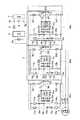
図1は実施例1の交流−直流変換装置を示す回路構成図である。図1に示す実施例1の交流−直流変換装置は、図3に示す従来の交流−直流変換装置に対して、以下の構成が異なる。実施例1では、3相(R相、S相、T相)の交流−直流変換装置について説明する。 FIG. 1 is a circuit configuration diagram illustrating an AC-DC converter according to a first embodiment. The AC-DC converter of Example 1 shown in FIG. 1 differs from the conventional AC-DC converter shown in FIG. In Example 1, a three-phase (R phase, S phase, T phase) AC-DC converter will be described.
トランス9は、交流端子2aと交流端子2cとの間で直列に接続される第1の1次巻線9a1と第2の1次巻線9a2と、交流端子2aと交流端子2bとの間で直列に接続される第1の1次巻線9b1と第2の1次巻線9b2と、交流端子2bと交流端子2cとの間で直列に接続される第1の1次巻線9c1と第2の1次巻線9c2と、2次巻線9dを有する。 The
半導体スイッチ素子(例えばGaN)からなる双方向スイッチQ1は、高電子移動度トランジスタ(HEMT;High Electron Mobility Transistor)Q1aのソース(一方の主端子)とHEMTQ1bのソースとが共通に接続された直列回路により構成されている。双方向スイッチQ2は、HEMTQ2aのソースとHEMTQ2bのソースが共通に接続された直列回路により構成されている。双方向スイッチQ3は、HEMTQ3aのソースとHEMTQ3bのソースとが共通に接続された直列回路により構成されている。HEMTは、窒化ガリウム(GaN)や炭化ケイ素(SiC)などのワイドバンドギャップ半導体から構成される。ここで、HEMTQ1a,Q1b、HEMTQ2a,Q2b、HEMTQ3a,Q3bのソースは、それぞれ双方向スイッチQ1,Q2,Q3の基準電位点である。 A bidirectional switch Q1 made of a semiconductor switch element (for example, GaN) is a series circuit in which a source (one main terminal) of a high electron mobility transistor (HEMT) Q1a and a source of a HEMTQ1b are connected in common. It is comprised by. The bidirectional switch Q2 is configured by a series circuit in which the source of the HEMT Q2a and the source of the HEMT Q2b are connected in common. The bidirectional switch Q3 is configured by a series circuit in which the source of the HEMT Q3a and the source of the HEMT Q3b are connected in common. The HEMT is composed of a wide band gap semiconductor such as gallium nitride (GaN) or silicon carbide (SiC). Here, the sources of the HEMTs Q1a, Q1b, HEMTQ2a, Q2b, HEMTQ3a, Q3b are reference potential points of the bidirectional switches Q1, Q2, Q3, respectively.
なお、実施例1では、双方向スイッチとしてHEMTを用いているが、HEMTに代えて、IGBT、MOSFET,JFETなどを用いても良い。 In the first embodiment, the HEMT is used as the bidirectional switch, but an IGBT, a MOSFET, a JFET, or the like may be used instead of the HEMT.
トランス9の第1の1次巻線9a1と双方向スイッチQ1とトランス9の第2の1次巻線9a2とが順番に直列に接続されて第1直列回路を構成する。トランス9の第1の1次巻線9a1の一端は交流端子2cに接続され、トランス9の第2の1次巻線9a2の一端は交流端子2aに接続されている。 The first primary winding 9a1 of the
トランス9の第1の1次巻線9b1と双方向スイッチQ2とトランス9の第2の1次巻線9b2とが順番に直列に接続されて第2直列回路を構成する。トランス9の第1の1次巻線9b1の一端は交流端子2aに接続され、トランス9の第2の1次巻線9b2の一端は交流端子2bに接続されている。 The first primary winding 9b1, the bidirectional switch Q2 of the
トランス9の第1の1次巻線9c1と双方向スイッチQ3とトランス9の第2の1次巻線9c2とが順番に直列に接続されて第3直列回路を構成する。トランス9の第1の1次巻線9c1の一端は交流端子2bに接続され、トランス9の第2の1次巻線9c2の一端は交流端子2cに接続されている。 The first primary winding 9c1 of the
トランス9の第1の1次巻線9a1,9b1,9c1の一端は抵抗13a,13b,13cの一端と抵抗17a,17b,17cの一端とに接続されている。トランス9の第2の1次巻線9a2,9b2,9c2の一端は抵抗16a,16b,16cの一端と抵抗20a,20b,20cの一端とに接続されている。抵抗13a,13b,13cの他端はダイオード14a,14b,14cのカソードに接続されている。 One end of the first primary winding 9a1, 9b1, 9c1 of the
ダイオード14a,14b,14cのアノードはダイオード15a,15b,15cのアノードとツェナーダイオード23a,23b,23cのアノードとコンデンサ24a,24b,24cの一端とスイッチSa2,Sb2,Sc2の一端とに接続されている。ダイオード15a,15b,15cのカソードは抵抗16a,16b,16cの他端に接続されている。 The anodes of the
抵抗17a,17b,17cの他端はダイオード18a,18b,18cのアノードに接続されている。ダイオード18a,18b,18cのカソードはダイオード19a,19b,19cのカソードとツェナーダイオード21a,21b,21cのカソードとコンデンサ22a,22b,22cの一端とスイッチSa1,Sb1,Sc1の一端とに接続されている。 The other ends of the
ツェナーダイオード21a,21b,21cのアノードとコンデンサ22a,22b,22cの他端とツェナーダイオード23a,23b,23cのカソードとコンデンサ24a,24b,24cの他端とは、HEMTQ1a,Q2a,Q3aのソースとHEMTQ1b,Q2b,Q3bのソースとに接続されている。スイッチSa1,Sb1,Sc1の他端とスイッチSa2,Sb2,Sc2の他端とはHEMTQ1a,Q2a,Q3aのゲート(制御端子)とHEMTQ1b,Q2b,Q3bのゲート(制御端子)とに接続されている。 The anodes of the
抵抗13a,16a,17a,20a、ダイオード14a,15a,18a,19a、ツェナーダイオード21a,23a、コンデンサ22a,24aは、3相交流電源1の交流電源電圧(R相とT相とによる線間電圧)から直流正電圧及び直流負電圧を生成する第1駆動回路電源生成回路を構成する。ゲート駆動回路12aは、第1駆動回路電源生成回路の直流正電圧及び直流負電圧を双方向スイッチQ1のゲートに印加することにより双方向スイッチQ1をオンオフさせる。 The
抵抗13b,16b,17b,20b、ダイオード14b,15b,18b,19b、ツェナーダイオード21b,23b、コンデンサ22b,24bは、3相交流電源1の交流電源電圧(R相とS相とによる線間電圧)から直流正電圧及び直流負電圧を生成する第2駆動回路電源生成回路を構成する。ゲート駆動回路12bは、第2駆動回路電源生成回路の直流正電圧及び直流負電圧を双方向スイッチQ2のゲートに印加することにより双方向スイッチQ2をオンオフさせる。 The
抵抗13c,16c,17c,20c、ダイオード14c,15c,18c,19c、ツェナーダイオード21c,23c、コンデンサ22c,24cは、3相交流電源1の交流電源電圧(S相とT相とによる線間電圧)から直流正電圧及び直流負電圧を生成する第3駆動回路電源生成回路を構成する。ゲート駆動回路12cは、第3駆動回路電源生成回路の直流正電圧及び直流負電圧を双方向スイッチQ3のゲートに印加することにより双方向スイッチQ3をオンオフさせる。
次にこのように構成された実施例1の交流−直流変換装置の動作を説明する。 Next, the operation of the thus configured AC-DC converter of Example 1 will be described.
まず、3相交流電源1からの交流電源電圧が交流端子2a〜2cを介して、トランス9の第1の1次巻線9a1と双方向スイッチQ1とトランス9の第2の1次巻線9a2との第1直列回路、トランス9の第1の1次巻線9b1と双方向スイッチQ2とトランス9の第2の1次巻線9b2との第2直列回路、トランス9の第1の1次巻線9c1と双方向スイッチQ3とトランス9の第2の1次巻線9c2との第3直列回路に印加される。 First, the AC power supply voltage from the three-phase AC power supply 1 is supplied via the
すると、例えば、交流端子2aと交流端子2cとの間では、3相交流電源1からの交流電源電圧により抵抗17a(20a)を介してダイオード18a(19a)で整流されてコンデンサ22aに直流正電圧が得られる。また、抵抗13a(16a)を介してダイオード14a(15a)で整流されてコンデンサ24aに直流負電圧が得られる。コンデンサ22aには上端が陽極で下端が陰極となる直流正電圧が得られる。 Then, for example, between the
コンデンサ24aには上端が陽極で下端が陰極となる直流負電圧が得られる。ここで、コンデンサ22aの下端及びコンデンサ24aの上端は第1駆動回路電源生成回路の基準電位点である。 The
このため、スイッチSa1をオンすることにより、コンデンサ22aの直流正電圧をHEMTQ1a,Q1bのゲートに印加すると、HEMTQ1a,Q1bをオンすることができる。また、スイッチSa2をオンすることにより、コンデンサ24aの直流負電圧をHEMTQ1a,Q1bのゲートに印加すると、HEMTQ1a,Q1bをオフすることができる。 For this reason, when the DC positive voltage of the
なお、その他の交流端子2aと交流端子2bとの間のトランス9の1次側回路、交流端子2bと交流端子2cとの間のトランス9の1次側回路についても、交流端子2aと交流端子2cとの間のトランス9の1次側回路と同様に動作するので、その説明は省略する。 In addition, also about the primary side circuit of the
このように、実施例1の交流−直流変換装置によれば、トランス9の第1の1次巻線9a1,9b1,9c1、双方向スイッチQ1,Q2,Q3、トランス9の第2の1次巻線9a2,9b2,9c2の順に直列に接続された直列回路及び双方向スイッチQ1,Q2,Q3をオンオフ駆動する駆動回路12a,12b,12cの正及び負電源を生成する駆動回路電源生成回路に交流電源電圧が印加されても、双方向スイッチQ1,Q2,Q3の基準電位点と駆動回路電源生成回路の基準電位点とが接続されているので、それぞれの基準電位点の電位が交流電源電圧の極性に関係なく交流電源電圧の中間電位になる。従って、非絶縁で簡単な回路で直流電源の電力を供給することができる。 Thus, according to the AC-DC converter of the first embodiment, the first primary windings 9a1, 9b1, 9c1, the bidirectional switches Q1, Q2, Q3 of the
図2は実施例2の交流−直流変換装置を示す回路構成図である。図1に示す実施例1の交流−直流変換装置は、単方向スイッチのHEMTを2つ直列に接続した2つの半導体スイッチ素子からなる双方向スイッチQ1〜Q3を用いたが、図2に示す実施例2の交流−直流変換装置は、双方向スイッチとして、1つの半導体スイッチ素子からなる双方向スイッチのHEMTQ4〜Q6を用いたことを特徴とする。 FIG. 2 is a circuit configuration diagram showing an AC-DC converter according to the second embodiment. The AC-DC converter of the first embodiment shown in FIG. 1 uses the bidirectional switches Q1 to Q3 including two semiconductor switch elements in which two unidirectional switch HEMTs are connected in series, but the implementation shown in FIG. The AC-DC converter of Example 2 is characterized in that the bidirectional switches HEMTQ4 to Q6 made up of one semiconductor switch element are used as the bidirectional switches.
その他の構成は、図1に示す構成と同一であるので、同一部分は同一符号を付し、その説明は省略する。 Since other configurations are the same as those shown in FIG. 1, the same portions are denoted by the same reference numerals, and the description thereof is omitted.
双方向スイッチのHEMTQ4,Q5,Q6は、ゲートGとドレインDとソースSとを有し、ドレインDにはダイオードD1,D3,D5のカソードが接続され、ダイオードD1,D3,D5のアノードとダイオードD2,D4,D6のアノードとは共通接続され、この接続点は仮想ソースIS1,IS2,IS3であるとともに、双方向スイッチQ4〜Q6の基準電位点でもある。この仮想ソースIS1,IS2,IS3には、コンデンサ22a,22b,22cとコンデンサ24a,24b,24cとの接続点とツェナーダイオード21a,21b,21cのアノードとツェナーダイオード23a,23b,23cのカソードとに接続されている。ダイオードD2,D4,D6のカソードは、双方向スイッチのHEMTQ4,Q5,Q6のソースSに接続されている。 The bidirectional switches HEMTs Q4, Q5, and Q6 have a gate G, a drain D, and a source S. The drains D are connected to the cathodes of diodes D1, D3, and D5, and the anodes and diodes of the diodes D1, D3, and D5 The anodes of D2, D4, and D6 are commonly connected, and this connection point is the virtual sources IS1, IS2, and IS3, and is also the reference potential point of the bidirectional switches Q4 to Q6. The virtual sources IS1, IS2, and IS3 include the connection points of the
このように、双方向スイッチのHEMTQ4〜Q6を用いても、実施例1の交流−直流変換装置と同様に動作し、同様な効果が得られる。また、双方向スイッチのHEMTQ4〜Q6は1つの半導体スイッチ素子であるので、安価となる。 Thus, even when the bidirectional switches HEMTQ4 to Q6 are used, they operate in the same manner as the AC-DC converter of the first embodiment, and the same effects are obtained. Further, since the HEMTs Q4 to Q6 of the bidirectional switches are one semiconductor switch element, they are inexpensive.
なお、本発明は、実施例1,2の交流−直流変換装置に限定されるものではない。実施例1,2の交流−直流変換装置では、3相交流電源に接続された交流−直流変換装置について説明したが、本発明は単相交流電源に接続された交流−直流変換装置にも適用可能である。この場合には、図1、図2に示す第1スイッチング回路50a,60aのみ用い、第2スイッチング回路50b,60b及び第3スイッチング回路50c,60cを削除すれば良い。 Note that the present invention is not limited to the AC-DC converters of the first and second embodiments. In the AC-DC converters of the first and second embodiments, the AC-DC converter connected to the three-phase AC power source has been described. However, the present invention is also applicable to the AC-DC converter connected to the single-phase AC power source. Is possible. In this case, only the
本発明は、通信用直流電源等に適用可能である。 The present invention is applicable to a DC power supply for communication.
1 3相交流電源
2a〜2c 交流端子
3,9 トランス
4 整流器
5 平滑リアクトル
7 負荷
8 平滑コンデンサ
9a1,9b1,9c1 第1の1次巻線
9a2,9b2,9c2 第2の1次巻線
9d 2次巻線
12a〜12c ゲート駆動回路
13a〜13c,16a〜16c,17a〜17c,20a〜20c 抵抗
21a〜21c,23a〜23c ツェナーダイオード
22a〜22c,24a〜24c コンデンサ
Q1〜Q3 双方向スイッチ
Q4〜Q6 双方向スイッチ
Q10,Q20,Q30 双方向スイッチ
D1〜D6,14a〜14c,15a〜15c,18a〜18c,19a〜19c ダイオード
50a,50b,50c スイッチング回路
60a,60b,60c スイッチング回路1 3-phase
4
8 Smoothing capacitors 9a1, 9b1, 9c1 First primary winding 9a2, 9b2, 9c2 Second primary winding 9d Secondary winding
12a-12c
Q10, Q20, Q30 Bidirectional switches D1-D6, 14a-14c, 15a-15c, 18a-18c, 19a-
Claims (2)
Translated fromJapanese前記トランスは、複数の1次巻線を有し、
前記スイッチング回路は、前記トランスの第1の1次巻線、双方向スイッチ、前記トランスの第2の1次巻線の順に直列に接続された直列回路と、前記直列回路の両端間に印加される交流電源電圧から直流正電圧及び直流負電圧を生成する駆動回路電源生成回路と、前記駆動回路電源生成回路と前記双方向スイッチとの間に接続されて前記双方向スイッチをオンオフ駆動する駆動回路とを有し、
前記双方向スイッチは、直列に接続された二つの半導体スイッチ素子からなり、互いに一方の主端子を接続し、この接続点を前記双方向スイッチの基準電位点とし、
前記双方向スイッチの基準電位点と前記駆動回路電源生成回路の基準電位点と
を接続したことを特徴とする交流−直流変換装置。By switching the switching circuit connected between the power lines of the single-phase AC power supply or between the power lines of the three-phase AC power supply, the current flowing in the primary winding of the transformer is interrupted and generated in the secondary winding of the transformer. In the AC-DC converter that rectifies and smoothes the voltage to be output to the load,
The transformer has a plurality of primary windings,
The switching circuit is applied between both ends of the series circuit and a series circuit connected in series in the order of the first primary winding of the transformer, a bidirectional switch, and the second primary winding of the transformer. Drive circuit power generation circuit for generating a DC positive voltage and a DC negative voltage from the AC power supply voltage, and a drive circuit connected between the drive circuit power generation circuit and the bidirectional switch to drive the bidirectional switch on and off And
The bidirectional switch is composed of two semiconductor switch elements connected in series, one main terminal is connected to each other, and this connection point is a reference potential point of the bidirectional switch,
An AC-DC converter characterized by connecting a reference potential point of the bidirectional switch and a reference potential point of the drive circuit power generation circuit.
前記トランスは、複数の1次巻線を有し、The transformer has a plurality of primary windings,
前記スイッチング回路は、前記トランスの第1の1次巻線、双方向スイッチ、前記トランスの第2の1次巻線の順に直列に接続された直列回路と、前記直列回路の両端間に印加される交流電源電圧から直流正電圧及び直流負電圧を生成する駆動回路電源生成回路と、前記駆動回路電源生成回路と前記双方向スイッチとの間に接続されて前記双方向スイッチをオンオフ駆動する駆動回路とを有し、The switching circuit is applied between both ends of the series circuit and a series circuit connected in series in the order of the first primary winding of the transformer, a bidirectional switch, and the second primary winding of the transformer. Drive circuit power generation circuit for generating a DC positive voltage and a DC negative voltage from the AC power supply voltage, and a drive circuit connected between the drive circuit power generation circuit and the bidirectional switch to drive the bidirectional switch on and off And
前記双方向スイッチは、一つの半導体スイッチ素子からなり、一方の主端子と他方の主端子との間には直列に接続された二つのダイオードが接続され、この二つのダイオードの接続点を前記双方向スイッチの基準電位点とし、 The bidirectional switch is composed of one semiconductor switch element, and two diodes connected in series are connected between one main terminal and the other main terminal, and a connection point of the two diodes is connected to the two terminals. The reference potential point of the direction switch,
前記双方向スイッチの基準電位点と前記駆動回路電源生成回路の基準電位点とA reference potential point of the bidirectional switch and a reference potential point of the drive circuit power generation circuit;
を接続したことを特徴とする交流−直流変換装置。The AC-DC converter characterized by having connected.
Priority Applications (2)
| Application Number | Priority Date | Filing Date | Title |
|---|---|---|---|
| JP2009297864AJP4968322B2 (en) | 2009-12-28 | 2009-12-28 | AC-DC converter |
| US12/949,423US8681511B2 (en) | 2009-12-28 | 2010-11-18 | Alternating current-direct current converter device |
Applications Claiming Priority (1)
| Application Number | Priority Date | Filing Date | Title |
|---|---|---|---|
| JP2009297864AJP4968322B2 (en) | 2009-12-28 | 2009-12-28 | AC-DC converter |
Publications (2)
| Publication Number | Publication Date |
|---|---|
| JP2011139591A JP2011139591A (en) | 2011-07-14 |
| JP4968322B2true JP4968322B2 (en) | 2012-07-04 |
Family
ID=44187364
Family Applications (1)
| Application Number | Title | Priority Date | Filing Date |
|---|---|---|---|
| JP2009297864AExpired - Fee RelatedJP4968322B2 (en) | 2009-12-28 | 2009-12-28 | AC-DC converter |
Country Status (2)
| Country | Link |
|---|---|
| US (1) | US8681511B2 (en) |
| JP (1) | JP4968322B2 (en) |
Families Citing this family (2)
| Publication number | Priority date | Publication date | Assignee | Title |
|---|---|---|---|---|
| US9244476B2 (en)* | 2012-03-02 | 2016-01-26 | Infineon Technologies Americas Corp. | Electronic ballast with power factor correction |
| US20230327553A1 (en)* | 2022-01-27 | 2023-10-12 | Astrodyne TDI | Power module formed with a switch-mode post-regulator to provide a high slew rate pulsed output current and/or voltage |
Family Cites Families (9)
| Publication number | Priority date | Publication date | Assignee | Title |
|---|---|---|---|---|
| JPH06245550A (en)* | 1993-02-22 | 1994-09-02 | Shibaura Eng Works Co Ltd | Power supply circuit |
| US6545450B1 (en)* | 1999-07-02 | 2003-04-08 | Advanced Energy Industries, Inc. | Multiple power converter system using combining transformers |
| JP3414719B2 (en) | 2001-01-31 | 2003-06-09 | サンケン電気株式会社 | Three-phase AC-DC converter |
| US7035125B2 (en)* | 2003-02-05 | 2006-04-25 | Matsushita Electric Industrial Co., Ltd. | Switching power supply and control method for the same |
| KR100497393B1 (en)* | 2003-06-20 | 2005-06-23 | 삼성전자주식회사 | Apparatus for improving power factor of power supply in a plasma display panel driving system and design method thereof |
| US7391132B2 (en)* | 2004-12-03 | 2008-06-24 | Huei-Jung Chen | Methods and apparatus providing double conversion/series-parallel hybrid operation in uninterruptible power supplies |
| US7164589B1 (en)* | 2005-07-11 | 2007-01-16 | International Rectifier Corporation | Bridgeless bi-directional forward type converter |
| US7746674B2 (en)* | 2007-02-22 | 2010-06-29 | Leader Electronics Inc. | Self-oscillating power converter |
| JP5369434B2 (en)* | 2007-12-21 | 2013-12-18 | サンケン電気株式会社 | Bidirectional switch |
- 2009
- 2009-12-28JPJP2009297864Apatent/JP4968322B2/ennot_activeExpired - Fee Related
- 2010
- 2010-11-18USUS12/949,423patent/US8681511B2/enactiveActive
Also Published As
| Publication number | Publication date |
|---|---|
| US8681511B2 (en) | 2014-03-25 |
| US20110157938A1 (en) | 2011-06-30 |
| JP2011139591A (en) | 2011-07-14 |
Similar Documents
| Publication | Publication Date | Title |
|---|---|---|
| CN102460932B (en) | power conversion device | |
| US7751212B2 (en) | Methods and apparatus for three-phase rectifier with lower voltage switches | |
| US5805437A (en) | Power electronic circuit arrangement having plural power converters | |
| JP2014117065A (en) | Parallel operation power unit | |
| JP2010518806A (en) | Inverter | |
| JP2007300712A (en) | Ac power feeding device | |
| EP3813243A1 (en) | Power switcher, power rectifier, and power converter | |
| CN110546874B (en) | Power conversion system | |
| US20140119079A1 (en) | Power factor correction circuit and power supply device including the same | |
| US6999325B2 (en) | Current/voltage converter arrangement | |
| JP6314734B2 (en) | Power converter | |
| CN101622778B (en) | DC power supply device | |
| US11569755B2 (en) | Active rectifier circuit with reduced complexity and reduced component count | |
| JP4968322B2 (en) | AC-DC converter | |
| JP7387663B2 (en) | Power conversion circuit and power conversion device | |
| JP5169590B2 (en) | Uninterruptible power supply and method for manufacturing the same | |
| JP5043585B2 (en) | Power converter | |
| JP2012191761A (en) | Ac-dc conversion circuit | |
| JP5590015B2 (en) | Inverter device and air conditioner equipped with the same | |
| WO2017090118A1 (en) | Power conversion device and rail vehicle | |
| CN109713906A (en) | A kind of controlled resonant converter | |
| JP2008099381A (en) | Power supply unit for arc welding, and the like | |
| JP6300845B2 (en) | Switching power supply circuit | |
| JPH11275865A (en) | Three-phase wide range input power converting circuit | |
| JP2000037076A (en) | Rectifying circuit |
Legal Events
| Date | Code | Title | Description |
|---|---|---|---|
| A977 | Report on retrieval | Free format text:JAPANESE INTERMEDIATE CODE: A971007 Effective date:20111031 | |
| A131 | Notification of reasons for refusal | Free format text:JAPANESE INTERMEDIATE CODE: A131 Effective date:20111129 | |
| A521 | Written amendment | Free format text:JAPANESE INTERMEDIATE CODE: A523 Effective date:20120120 | |
| TRDD | Decision of grant or rejection written | ||
| A01 | Written decision to grant a patent or to grant a registration (utility model) | Free format text:JAPANESE INTERMEDIATE CODE: A01 Effective date:20120306 | |
| A01 | Written decision to grant a patent or to grant a registration (utility model) | Free format text:JAPANESE INTERMEDIATE CODE: A01 | |
| A61 | First payment of annual fees (during grant procedure) | Free format text:JAPANESE INTERMEDIATE CODE: A61 Effective date:20120319 | |
| FPAY | Renewal fee payment (event date is renewal date of database) | Free format text:PAYMENT UNTIL: 20150413 Year of fee payment:3 | |
| R150 | Certificate of patent or registration of utility model | Free format text:JAPANESE INTERMEDIATE CODE: R150 | |
| LAPS | Cancellation because of no payment of annual fees |