JP4967780B2 - Coordinate input device and display device - Google Patents
Coordinate input device and display deviceDownload PDFInfo
- Publication number
- JP4967780B2 JP4967780B2JP2007111480AJP2007111480AJP4967780B2JP 4967780 B2JP4967780 B2JP 4967780B2JP 2007111480 AJP2007111480 AJP 2007111480AJP 2007111480 AJP2007111480 AJP 2007111480AJP 4967780 B2JP4967780 B2JP 4967780B2
- Authority
- JP
- Japan
- Prior art keywords
- detection
- detection electrode
- coordinate
- capacitance
- pair
- Prior art date
- Legal status (The legal status is an assumption and is not a legal conclusion. Google has not performed a legal analysis and makes no representation as to the accuracy of the status listed.)
- Active
Links
Images


Classifications
- G—PHYSICS
- G06—COMPUTING OR CALCULATING; COUNTING
- G06F—ELECTRIC DIGITAL DATA PROCESSING
- G06F3/00—Input arrangements for transferring data to be processed into a form capable of being handled by the computer; Output arrangements for transferring data from processing unit to output unit, e.g. interface arrangements
- G06F3/01—Input arrangements or combined input and output arrangements for interaction between user and computer
- G06F3/03—Arrangements for converting the position or the displacement of a member into a coded form
- G06F3/041—Digitisers, e.g. for touch screens or touch pads, characterised by the transducing means
- G06F3/044—Digitisers, e.g. for touch screens or touch pads, characterised by the transducing means by capacitive means
- G06F3/0443—Digitisers, e.g. for touch screens or touch pads, characterised by the transducing means by capacitive means using a single layer of sensing electrodes
- G—PHYSICS
- G06—COMPUTING OR CALCULATING; COUNTING
- G06F—ELECTRIC DIGITAL DATA PROCESSING
- G06F3/00—Input arrangements for transferring data to be processed into a form capable of being handled by the computer; Output arrangements for transferring data from processing unit to output unit, e.g. interface arrangements
- G06F3/01—Input arrangements or combined input and output arrangements for interaction between user and computer
- G06F3/03—Arrangements for converting the position or the displacement of a member into a coded form
- G06F3/041—Digitisers, e.g. for touch screens or touch pads, characterised by the transducing means
- G06F3/044—Digitisers, e.g. for touch screens or touch pads, characterised by the transducing means by capacitive means
- G06F3/0446—Digitisers, e.g. for touch screens or touch pads, characterised by the transducing means by capacitive means using a grid-like structure of electrodes in at least two directions, e.g. using row and column electrodes
- G—PHYSICS
- G06—COMPUTING OR CALCULATING; COUNTING
- G06F—ELECTRIC DIGITAL DATA PROCESSING
- G06F3/00—Input arrangements for transferring data to be processed into a form capable of being handled by the computer; Output arrangements for transferring data from processing unit to output unit, e.g. interface arrangements
- G06F3/01—Input arrangements or combined input and output arrangements for interaction between user and computer
- G06F3/03—Arrangements for converting the position or the displacement of a member into a coded form
- G06F3/033—Pointing devices displaced or positioned by the user, e.g. mice, trackballs, pens or joysticks; Accessories therefor
- G06F3/0354—Pointing devices displaced or positioned by the user, e.g. mice, trackballs, pens or joysticks; Accessories therefor with detection of 2D relative movements between the device, or an operating part thereof, and a plane or surface, e.g. 2D mice, trackballs, pens or pucks
- G—PHYSICS
- G06—COMPUTING OR CALCULATING; COUNTING
- G06F—ELECTRIC DIGITAL DATA PROCESSING
- G06F3/00—Input arrangements for transferring data to be processed into a form capable of being handled by the computer; Output arrangements for transferring data from processing unit to output unit, e.g. interface arrangements
- G06F3/01—Input arrangements or combined input and output arrangements for interaction between user and computer
- G06F3/03—Arrangements for converting the position or the displacement of a member into a coded form
- G06F3/041—Digitisers, e.g. for touch screens or touch pads, characterised by the transducing means
- G06F3/0412—Digitisers structurally integrated in a display
- G—PHYSICS
- G06—COMPUTING OR CALCULATING; COUNTING
- G06F—ELECTRIC DIGITAL DATA PROCESSING
- G06F3/00—Input arrangements for transferring data to be processed into a form capable of being handled by the computer; Output arrangements for transferring data from processing unit to output unit, e.g. interface arrangements
- G06F3/01—Input arrangements or combined input and output arrangements for interaction between user and computer
- G06F3/03—Arrangements for converting the position or the displacement of a member into a coded form
- G06F3/041—Digitisers, e.g. for touch screens or touch pads, characterised by the transducing means
- G06F3/0416—Control or interface arrangements specially adapted for digitisers
- G—PHYSICS
- G06—COMPUTING OR CALCULATING; COUNTING
- G06F—ELECTRIC DIGITAL DATA PROCESSING
- G06F3/00—Input arrangements for transferring data to be processed into a form capable of being handled by the computer; Output arrangements for transferring data from processing unit to output unit, e.g. interface arrangements
- G06F3/01—Input arrangements or combined input and output arrangements for interaction between user and computer
- G06F3/03—Arrangements for converting the position or the displacement of a member into a coded form
- G06F3/041—Digitisers, e.g. for touch screens or touch pads, characterised by the transducing means
- G06F3/044—Digitisers, e.g. for touch screens or touch pads, characterised by the transducing means by capacitive means
- G06F3/0448—Details of the electrode shape, e.g. for enhancing the detection of touches, for generating specific electric field shapes, for enhancing display quality
Landscapes
- Engineering & Computer Science (AREA)
- General Engineering & Computer Science (AREA)
- Theoretical Computer Science (AREA)
- Human Computer Interaction (AREA)
- Physics & Mathematics (AREA)
- General Physics & Mathematics (AREA)
- Quality & Reliability (AREA)
- Position Input By Displaying (AREA)
Description
Translated fromJapanese本発明は、例えばタッチパネルなどの座標入力装置及び表示装置に関するものである。 The present invention relates to a coordinate input device such as a touch panel and a display device.
近年、PDA(Personal Digital Assistant:携帯情報端末機)やノート型パーソナルコンピュータなどの小型情報電子機器の普及に伴い、表示画面上に指やペンなどの物体を接触させることにより入力操作を行う、いわゆるタッチパネル機能が付加された表示装置が広く利用されている。このようなタッチパネルにおいて、指などの接触位置を検出する方法として静電容量方式がある。静電容量方式は、人間が指で表示面に触れることによって形成された静電容量を介して微弱な電流を流し、この電流量から接触位置の検出を行う方式である。ここで、静電容量方式では、平面状に形成された検出電極と検出電極上に積層された誘電体膜とを用いており、誘電体膜を指などで触れることで静電容量を形成している。 In recent years, with the spread of small information electronic devices such as PDAs (Personal Digital Assistants) and notebook personal computers, so-called input operations are performed by bringing an object such as a finger or a pen into contact with a display screen. Display devices to which a touch panel function is added are widely used. In such a touch panel, there is a capacitance method as a method for detecting a contact position of a finger or the like. The capacitance method is a method in which a weak current is passed through a capacitance formed by a person touching a display surface with a finger, and a contact position is detected from this amount of current. Here, the capacitance method uses a detection electrode formed in a planar shape and a dielectric film laminated on the detection electrode, and the capacitance is formed by touching the dielectric film with a finger or the like. ing.
静電容量方式を用いたタッチパネルでは、二次元座標を検出する方法として、X座標を求めるための検出電極とY座標を求めるための検出電極とを用いてX座標及びY座標をそれぞれ求める方法がある(例えば、特許文献1から3参照)。
しかしながら、上記従来の座標入力装置においても、以下の課題が残されている。すなわち、電気的な絶縁状態を確保するため、X座標を求めるための検出電極とY座標を求めるための検出電極とを絶縁膜を介した異なる層上に形成したり、絶縁膜を介した異なる2層上に配線を形成したりすることで立体的に交差させている。そのため、絶縁膜の上下層に検出電極や配線を形成する必要があり、少なくとも3層構造となる。したがって、製造工程が複雑になるという問題がある。 However, the following problems remain in the conventional coordinate input device. That is, in order to secure an electrical insulation state, the detection electrode for obtaining the X coordinate and the detection electrode for obtaining the Y coordinate are formed on different layers through the insulating film, or different through the insulating film. Crossing in a three-dimensional manner by forming wiring on two layers. Therefore, it is necessary to form detection electrodes and wirings in the upper and lower layers of the insulating film, and at least a three-layer structure is obtained. Therefore, there is a problem that the manufacturing process becomes complicated.
本発明は、上記従来の問題に鑑みてなされたもので、製造工程の簡略化が可能な座標入力装置及び表示装置を提供することを目的とする。 The present invention has been made in view of the above-described conventional problems, and an object thereof is to provide a coordinate input device and a display device capable of simplifying the manufacturing process.
本発明は、前記課題を解決するために以下の構成を採用した。すなわち、本発明にかかる座標入力装置は、基板上の検出領域内で平面状に配置された複数の検出電極と、該複数の検出電極のそれぞれに接続された複数の引廻配線と、前記複数の検出電極を被覆する被覆膜と、該被覆膜を介して前記複数の検出電極と被検出物との間に形成される静電容量の変化を検出する検出手段と、該検出手段の検出結果から前記静電容量の形成位置を算出する算出手段とを備え、前記複数の検出電極が、前記検出領域内の第1方向に沿って形成されると共に、該第1方向と交差する第2方向に沿って配列され、隣り合う一対の前記検出電極により検出電極対を複数構成し、該検出電極対を構成する前記一対の検出電極の一方の幅と他方の幅との比率が、前記第1方向に沿って変化し、前記複数の引廻配線のそれぞれが、前記検出電極のうち前記第1方向のいずれかの端部に接続されると共に、前記複数の検出電極と同層上に形成されており、前記複数の検出電極の外形が、それぞれ合同であり、前記検出電極対を構成する前記一方の検出電極の幅が、前記第1方向で一方から他方に向かうにしたがって小さくなり、前記他方の検出電極の幅が、前記第1方向で一方から他方に向かうにしたがって大きくなっており、前記複数の検出電極の前記第1方向に沿う一対の側辺が、直線状であり、前記複数の検出電極が、前記検出電極対を構成する前記一方の検出電極と該一方の検出電極と隣り合う他の前記検出電極対を構成する前記他方の検出電極とにより補正検出電極対を構成し、前記算出手段が、前記一方の検出電極での前記静電容量の変化量の和と、前記他方の検出電極での前記静電容量の変化量の和とに基づいて、前記第1方向での前記検出位置である第1座標を算出する第1座標算出手段と、前記各検出電極対での前記静電容量の変化量と、前記一方の検出電極及び該一方の検出電極と隣り合う他の前記検出電極対を構成する前記他方の検出電極での前記静電容量の変化量と、前記第1座標とから、前記第2方向での前記検出位置である第2座標を算出する第2座標算出手段とを備え、前記第2座標算出手段は、前記検出電極対の幅方向の中心線に対する前記補正検出電極対の幅方向の中心線の傾きに基づいて補正した前記第1座標を用いて前記第2座標を算出することを特徴とする。
本発明にかかる座標入力装置は、基板上の検出領域内で平面状に配置された複数の検出電極と、該複数の検出電極のそれぞれに接続された複数の引廻配線と、前記複数の検出電極を被覆する被覆膜と、該被覆膜を介して前記複数の検出電極との間に形成される静電容量の変化を検出する検出手段と、該検出手段の検出結果から前記静電容量の形成位置を算出する算出手段とを備え、前記複数の検出電極が、前記検出領域内の第1方向に沿って形成されると共に、該第1方向と交差する第2方向に沿って配列され、隣り合う一対の前記検出電極により検出電極対を複数構成し、該検出電極対を構成する前記一対の検出電極の一方の幅と他方の幅との比率が、前記第1方向に沿って変化し、前記複数の引廻配線のそれぞれが、前記検出電極のうち前記第1方向のいずれかの端部に接続されると共に、前記複数の検出電極と同層上に形成されていることを特徴とする。The present invention employs the following configuration in order to solve the above problems. That is, the coordinate input device according to the present invention includesa plurality of detection electrodes arranged in a plane within a detection region on a substrate, a plurality of routing wires connected to each of the plurality of detection electrodes, A coating film that covers the detection electrode, a detection unit that detects a change in capacitance formed between the plurality of detection electrodes and the object to be detected via the coating film, and Calculation means for calculating the formation position of the capacitance from the detection result, and the plurality of detection electrodes are formed along a first direction in the detection region and intersect with the first direction. A plurality of detection electrode pairs are constituted by a pair of adjacent detection electrodes arranged along two directions, and the ratio of the width of one of the pair of detection electrodes constituting the detection electrode pair to the width of the other is Change along the first direction, each of the plurality of routing wires The detection electrodes are connected to any one end in the first direction and are formed on the same layer as the plurality of detection electrodes, and the outer shapes of the plurality of detection electrodes are respectively congruent, The width of the one detection electrode constituting the detection electrode pair decreases from one to the other in the first direction, and the width of the other detection electrode decreases from one to the other in the first direction. A pair of side edges along the first direction of the plurality of detection electrodes are linear, and the plurality of detection electrodes and the one detection electrode constituting the detection electrode pair A correction detection electrode pair is constituted by the other detection electrode pair constituting the other detection electrode pair adjacent to the one detection electrode, and the calculation means changes the capacitance at the one detection electrode. Sum of quantities and other First coordinate calculation means for calculating a first coordinate which is the detection position in the first direction based on the sum of the amount of change in the capacitance at the detection electrode, and at each detection electrode pair The amount of change in capacitance, the amount of change in capacitance in the other detection electrode constituting the one detection electrode and the other detection electrode pair adjacent to the one detection electrode, and the first Second coordinate calculation means for calculating a second coordinate that is the detection position in the second direction from one coordinate, and the second coordinate calculation means is for a center line in the width direction of the detection electrode pair. The second coordinates are calculated using the first coordinates corrected based on the inclination of the center line in the width direction of the correction detection electrode pair.
A coordinate input device according to the present invention includes a plurality of detection electrodes arranged in a plane within a detection region on a substrate, a plurality of lead wires connected to each of the plurality of detection electrodes, and the plurality of detections. A coating film that coats the electrode; a detection unit that detects a change in capacitance formed between the plurality of detection electrodes via the coating film; and the electrostatic capacitance based on a detection result of the detection unit. And a plurality of detection electrodes formed along a first direction in the detection region and arranged along a second direction intersecting the first direction. A plurality of detection electrode pairs are configured by a pair of adjacent detection electrodes, and a ratio of one width to the other width of the pair of detection electrodes constituting the detection electrode pair is along the first direction. Each of the plurality of routing wirings out of the detection electrodes. Serial is connected to one end of the first direction, characterized in that it is formed on the plurality of detection electrodes and the same layer on.
この発明では、検出電極と引廻配線とを同層上に形成することで、製造工程が簡略化する。すなわち、第1方向に沿って形成された検出電極の第1方向における端部において、検出電極と引廻配線とを接続することで、複数の検出電極から引き廻された引廻配線同士を交差させる必要がなくなる。したがって、検出電極及び引廻配線を同層上に形成でき、製造工程の簡略化及び製造コストの削減が図れる。
ここで、検出電極対を構成する2つの検出電極の幅の比率を第1方向に沿って変化させることで、指などの接触により静電容量が形成されたとき、検出電極対を構成する一方の検出電極で検出される静電容量の変化量と他方の検出電極で検出される静電容量の変化量との比率が静電容量の形成位置に応じて変化する。そして、算出手段は、この検出結果の違いから、第1方向における静電容量の形成位置を算出する。また、第2方向に沿って帯状の複数の検出電極対を配置することで、静電容量が形成されたとき、検出電極対ごとで検出される変化量の比率が静電容量の形成位置に応じて変化する。そして、算出手段は、この検出結果の違いから、第2方向における静電容量の形成位置を算出する。このようにして、算出手段は、静電容量の形成位置に応じた二次元座標を算出する。In the present invention, the manufacturing process is simplified by forming the detection electrode and the lead wiring on the same layer. That is, at the end in the first direction of the detection electrode formed along the first direction, the detection electrode and the routing wiring are connected to cross the routing wirings routed from the plurality of detection electrodes. There is no need to let them. Therefore, the detection electrode and the lead wiring can be formed on the same layer, and the manufacturing process can be simplified and the manufacturing cost can be reduced.
Here, by changing the ratio of the widths of the two detection electrodes constituting the detection electrode pair along the first direction, when the electrostatic capacitance is formed by contact with a finger or the like, The ratio between the amount of change in capacitance detected by the first detection electrode and the amount of change in capacitance detected by the other detection electrode changes according to the position where the capacitance is formed. And a calculation means calculates the formation position of the electrostatic capacitance in a 1st direction from the difference in this detection result. Further, by arranging a plurality of strip-shaped detection electrode pairs along the second direction, when the capacitance is formed, the ratio of the amount of change detected for each detection electrode pair is the capacitance formation position. Will change accordingly. And a calculation means calculates the formation position of the electrostatic capacitance in a 2nd direction from the difference in this detection result. In this way, the calculation means calculates two-dimensional coordinates corresponding to the capacitance formation position.
また、本発明の座標入力装置は、前記複数の検出電極の外形が、それぞれ合同であり、前記検出電極対を構成する前記一方の検出電極の幅が、前記第1方向で一方から他方に向かうにしたがって小さくなり、前記他方の検出電極の幅が、前記第1方向で一方から他方に向かうにしたがって大きくなることが好ましい。
この発明では、検出電極の形状を同一とすることで、算出手段による二次元座標の検出を容易に行うことができる。In the coordinate input device of the present invention, the outer shapes of the plurality of detection electrodes are congruent, and the width of the one detection electrode constituting the detection electrode pair is from one to the other in the first direction. It is preferable that the width of the other detection electrode becomes smaller as the width of the second detection electrode increases from one to the other in the first direction.
In this invention, by making the shapes of the detection electrodes the same, the two-dimensional coordinates can be easily detected by the calculating means.
また、本発明の座標入力装置は、前記複数の検出電極の前記第1方向に沿う一対の側辺が、直線状であることが好ましい。
この発明では、側辺を直線状にすることで複数の検出電極を密に配置できる。これにより、算出手段による二次元座標の検出精度が向上する。In the coordinate input device of the present invention, it is preferable that the pair of side sides along the first direction of the plurality of detection electrodes is linear.
In the present invention, the plurality of detection electrodes can be densely arranged by making the side sides linear. Thereby, the detection precision of the two-dimensional coordinate by a calculation means improves.
また、本発明の座標入力装置は、前記一対の側辺は、一方が前記第1方向と平行であると共に、他方が前記第1及び第2方向から傾いており、前記検出電極対を構成する前記一対の検出電極は、前記他方の側辺が対向配置されていることが好ましい。
この発明では、検出電極対の外形が、第1方向と平行である一対の辺を有するほぼ等幅の帯状になる。これにより、第2方向における静電容量の形成位置の算出が容易になると共にその検出精度が向上する。ここで、第1及び第2方向が互いに直交する場合には、検出電極対の外形がほぼ矩形状になる。In the coordinate input device of the present invention, one of the pair of side sides is parallel to the first direction, and the other is inclined from the first and second directions, and constitutes the detection electrode pair. It is preferable that the other side of the pair of detection electrodes is arranged to face each other.
In the present invention, the outer shape of the detection electrode pair is a strip having a substantially equal width having a pair of sides parallel to the first direction. This facilitates calculation of the capacitance formation position in the second direction and improves the detection accuracy. Here, when the first and second directions are orthogonal to each other, the outer shape of the detection electrode pair is substantially rectangular.
また、本発明の座標入力装置は、前記算出手段が、前記一方の検出電極での前記静電容量の変化量の和と、前記他方の検出電極での前記静電容量の変化量の和とに基づいて、前記第1方向での前記検出位置である第1座標を算出する第1座標算出手段と、前記各検出電極対での前記静電容量の変化量から、前記第2方向での前記検出位置である第2座標を算出する第2座標算出手段とを備えることとしてもよい。
この発明では、第1座標算出手段が、検出電極対を構成する一対の検出電極の一方で検出される静電容量と他方で検出される静電容量の変化量の比率から、第1方向における静電容量の形成位置である第1座標を算出する。また、第2座標算出手段が、各検出電極対で検出される静電容量の変化量の比率から、第2方向における静電容量の形成位置である第2座標を算出する。Further, in the coordinate input device of the present invention, the calculation means includes a sum of the amount of change in the capacitance at the one detection electrode and a sum of the amount of change in the capacitance at the other detection electrode. Based on the first coordinate calculation means for calculating the first coordinate that is the detection position in the first direction, and the change amount of the capacitance in each detection electrode pair, in the second direction It is good also as providing the 2nd coordinate calculation means which calculates the 2nd coordinate which is the said detection position.
In the present invention, the first coordinate calculation means determines the first direction in the first direction from the ratio between the capacitance detected by one of the pair of detection electrodes constituting the detection electrode pair and the change in capacitance detected by the other. A first coordinate that is a capacitance forming position is calculated. Further, the second coordinate calculation means calculates the second coordinate that is the electrostatic capacitance forming position in the second direction from the ratio of the change amount of the electrostatic capacitance detected by each detection electrode pair.
また、本発明の座標入力装置は、前記複数の検出電極が、前記検出電極対を構成する前記一方の検出電極と該一方の検出電極と隣り合う他の前記検出電極対を構成する前記他方の検出電極とにより補正検出電極対を構成し、前記算出手段が、前記一方の検出電極での前記静電容量の変化量の和と、前記他方の検出電極での前記静電容量の変化量の和とに基づいて、前記第1方向での前記検出位置である第1座標を算出する第1座標算出手段と、前記各検出電極対での前記静電容量の変化量と、前記一方の検出電極及び該一方の検出電極と隣り合う他の前記検出電極対を構成する前記他方の検出電極での前記静電容量の変化量と、前記第1座標とから、前記第2方向での前記検出位置である第2座標を算出する第2座標算出手段とを備えることとしてもよい。
この発明では、各検出電極対での静電容量の変化量に加えて、補正検出電極対での静電容量の変化量に第1座標の値を考慮して第2座標を算出することで、第2座標の算出精度が向上する。In the coordinate input device according to the present invention, the plurality of detection electrodes may include the one detection electrode constituting the detection electrode pair and the other detection electrode pair adjacent to the one detection electrode. A correction detection electrode pair is constituted by the detection electrode, and the calculation means calculates the sum of the change amount of the capacitance at the one detection electrode and the change amount of the capacitance at the other detection electrode. Based on the sum, first coordinate calculation means for calculating the first coordinate which is the detection position in the first direction, the amount of change in the capacitance at each detection electrode pair, and the detection of the one The detection in the second direction from the amount of change in the capacitance at the other detection electrode constituting the electrode and the other detection electrode pair adjacent to the one detection electrode, and the first coordinates Second coordinate calculation means for calculating a second coordinate as a position It may be.
In this invention, in addition to the amount of change in capacitance at each detection electrode pair, the second coordinate is calculated in consideration of the value of the first coordinate in the amount of change in capacitance at the corrected detection electrode pair. The calculation accuracy of the second coordinate is improved.
また、本発明の座標入力装置は、前記第2座標算出手段が、前記検出電極対の幅方向の中心線に対する前記補正検出電極対の幅方向の中心線の傾きに基づいて補正した前記第2座標を算出することとしてもよい。
この発明では、検出電極対の延在方向と、補正検出電極対の延在方向とが異なることから、互いの中心軸の傾きを考慮して第2座標を算出することで、第2座標の算出精度が向上する。In the coordinate input device of the present invention, the second coordinate calculation unit corrects the second correction based on the inclination of the center line in the width direction of the correction detection electrode pair with respect to the center line in the width direction of the detection electrode pair. Coordinates may be calculated.
In this invention, since the extension direction of the detection electrode pair is different from the extension direction of the correction detection electrode pair, the second coordinate is calculated by considering the inclination of the center axis of each other. Calculation accuracy is improved.
また、本発明の座標入力装置は、前記算出手段が、前記一方の検出電極での前記静電容量の変化量の和と、前記他方の検出電極での前記静電容量の変化量の和とに基づいて、前記第1方向での前記検出位置である第1座標を算出する第1座標算出手段と、前記一方の検出電極での前記静電容量の変化量の和と、前記他方の検出電極での前記静電容量の変化量の和とに基づいて前記第2方向での前記検出位置である第2座標を算出する第2座標算出手段とを備えることとしてもよい。
この発明では、一方の検出電極と他方の検出電極とで個別に静電容量の変化量の和を算出し、これに基づいて第2座標を算出する。Further, in the coordinate input device of the present invention, the calculation means includes a sum of the amount of change in the capacitance at the one detection electrode and a sum of the amount of change in the capacitance at the other detection electrode. Based on the first coordinate calculation means for calculating the first coordinate which is the detection position in the first direction, the sum of the amount of change in the capacitance at the one detection electrode, and the detection of the other Second coordinate calculation means may be provided that calculates a second coordinate that is the detection position in the second direction based on the sum of the amount of change in the capacitance at the electrode.
In this invention, the sum of the amount of change in electrostatic capacitance is calculated individually for one detection electrode and the other detection electrode, and the second coordinates are calculated based on this.
また、本発明の座標入力装置は、前記複数の引廻配線のそれぞれが、前記検出電極のうち前記第1方向の一方の端部に接続されていることが好ましい。
この発明では、引廻配線による引き廻し長さを短くすることができる。これにより、引廻配線の構成材料として、抵抗率の高い材料により構成されている検出電極と同一材料を用いることができる。したがって、検出電極と引廻配線とを同一工程で形成でき、製造工程をさらに簡略化できると共に、製造コストをさらに削減できる。In the coordinate input device of the present invention, it is preferable that each of the plurality of lead wires is connected to one end portion in the first direction of the detection electrodes.
In the present invention, the routing length by the routing wiring can be shortened. Thereby, the same material as that of the detection electrode made of a material having a high resistivity can be used as a constituent material of the lead wiring. Therefore, the detection electrode and the lead wiring can be formed in the same process, the manufacturing process can be further simplified, and the manufacturing cost can be further reduced.
また、本発明の表示装置は、上記記載の座標入力装置と、前記基板と電気光学層を介して対向配置された他の基板とを有することを特徴とする。
この発明では、上述と同様に、検出電極及び引廻配線を同層上に形成できるので、製造工程の簡略化及び製造コストの削減が図れる。According to another aspect of the present invention, there is provided a display device including the coordinate input device described above, and another substrate disposed opposite to the substrate via an electro-optic layer.
In the present invention, since the detection electrode and the lead-out wiring can be formed on the same layer as described above, the manufacturing process can be simplified and the manufacturing cost can be reduced.
また、本発明の表示装置は、前記複数の検出電極が、前記基板のうち前記電気光学層から離間する側に形成されていることが好ましい。
この発明では、複数の検出電極を表示装置の外面側に設けることで、指などの接触位置の検出精度を向上させることができる。In the display device of the present invention, it is preferable that the plurality of detection electrodes are formed on a side of the substrate that is separated from the electro-optic layer.
In this invention, the detection accuracy of contact positions, such as a finger | toe, can be improved by providing a some detection electrode in the outer surface side of a display apparatus.
また、本発明の表示装置は、前記複数の検出電極が、前記基板のうち前記電気光学層側に形成されていることが好ましい。
この発明では、表示装置を構成する部材と複数の検出電極及び引廻配線とを基板の同一面側に形成することで、製造工程の簡略化が図れる。In the display device of the present invention, it is preferable that the plurality of detection electrodes are formed on the electro-optic layer side of the substrate.
According to the present invention, the manufacturing process can be simplified by forming the members constituting the display device, the plurality of detection electrodes and the lead wiring on the same surface side of the substrate.
[第1の実施形態]
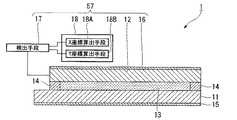
以下、本発明における座標入力装置及び表示装置の第1の実施形態を、図面に基づいて説明する。なお、以下の説明に用いる各図面では、各部材を認識可能な大きさとするために縮尺を適宜変更している。ここで、図1は表示装置を示す概略構成図、図2は表示装置の等価回路図、図3は表示装置を示す断面図、図4は対向基板の外面側を示す平面図である。[First Embodiment]
Hereinafter, a coordinate input device and a display device according to a first embodiment of the present invention will be described with reference to the drawings. In each drawing used in the following description, the scale is appropriately changed to make each member a recognizable size. Here, FIG. 1 is a schematic configuration diagram showing the display device, FIG. 2 is an equivalent circuit diagram of the display device, FIG. 3 is a sectional view showing the display device, and FIG. 4 is a plan view showing the outer surface side of the counter substrate.
〔表示装置〕
本実施形態における表示装置1は、透過型のカラー液晶表示であって、R(赤)、G(緑)、B(青)の各色光を出力する3個のサブ画素領域で1個の画素を構成する液晶表示装置である。ここで、表示を構成する最小単位となる表示領域を「サブ画素領域」と称する。
最初に、本実施形態における表示装置の概略構成について説明する。本実施形態における表示装置1は、図1に示すように、アクティブマトリックス基板である素子基板(他の基板)11と、素子基板11と対向配置された対向基板(基板)12と、素子基板11及び対向基板12に挟持された液晶層(電気光学層)13とを備えている。
そして、表示装置1は、素子基板11と対向基板12とが対向する対向領域の外周部に設けられた平面視でほぼ矩形の枠状のシール材14を有しており、このシール材14によって素子基板11と対向基板12とが貼り合わされている。ここで、表示装置1のうちシール材14のうち側に、画像表示領域が形成される。また、表示装置1は、素子基板11の外面側(液晶層13から離間する側)から照明光を照射する構成となっている。
さらに、表示装置1は、素子基板11の外面側に設けられた偏光板15及び対向基板12の外面側(液晶層13から離間する側)に設けられた偏光板16を備えている。また、表示装置1は、検出手段17及び算出手段18を備えている。[Display device]
The
First, a schematic configuration of the display device in the present embodiment will be described. As shown in FIG. 1, the
The
Further, the
また、表示装置1の画像表示領域には、図2に示すように、複数のサブ画素領域がマトリックス状に配置されている。この複数のサブ画素領域のそれぞれには、画素電極21と、画素電極をスイッチング制御するためのTFT(Thin Film Transistor:薄膜トランジスタ)素子22とが形成されている。また、画像表示領域には、複数のデータ線23及び走査線24が格子状に配置されている。 In the image display area of the
TFT素子22は、ソースがデータ線23に接続され、ゲートが走査線24に接続され、ドレインが画素電極21に接続されている。
データ線23は、表示装置1に設けられた駆動回路(図示略)から供給される画像信号S1、S2、…、Snを各サブ画素領域に供給する構成となっている。ここで、データ線23は、画像信号S1〜Snをこの順で線順次で供給してもよく、互いに隣接する複数のデータ線23同士に対してグループごとに供給してもよい。
走査線24は、表示装置1に設けられた駆動回路(図示略)から供給される走査信号G1、G2、…、Gmを各サブ画素領域に供給する構成となっている。ここで、走査線24は、走査信号G1〜Gmを所定のタイミングでパルス的に線順次で供給する構成となっている。The
The
The
また、表示装置1は、スイッチング素子であるTFT素子22が走査信号G1〜Gmの入力により一定期間だけオン状態とされることで、データ線23から供給される画像信号S1〜Snが所定のタイミングで画素電極21に書き込まれる構成となっている。そして、画素電極21を介して液晶に書き込まれた所定レベルの画像信号S1〜Snは、画素電極21と後述する共通電極36との間で一定期間保持される。 Further, in the
次に、表示装置1の詳細な構成について、図3及び図4を参照しながら説明する。
素子基板11は、図3に示すように、例えばガラスや石英、プラスチックなどの透光性材料からなる基板本体31と、基板本体31の内側(液晶層13側)の表面に順に形成された素子形成層32、層間絶縁膜33、電極絶縁膜34及び配向膜35とを備えている。また、素子基板11は、層間絶縁膜33の内側の表面に配置された共通電極36と、電極絶縁膜34の内側の表面に配置された画素電極21とを備えている。Next, a detailed configuration of the
As shown in FIG. 3, the
素子形成層32は、絶縁膜や半導体膜、導体膜を積層した構成となっており、図2に示すデータ線23や走査線24などの配線部とTFT素子22を構成している。
層間絶縁膜33は、例えばアクリルなどの透光性材料で構成されており、素子形成層32を覆うように設けられている。
電極絶縁膜34は、例えばSiNなどの透光性材料で構成されており、層間絶縁膜33上に形成された共通電極36を覆うように設けられている。
配向膜35は、例えばポリイミドなどの樹脂材料で構成されており、電極絶縁膜34上に形成された画素電極21を覆うように設けられている。また、配向膜35の表面には、液晶層13を構成する液晶分子の初期配向状態を規制するための配向処理が施されている。The
The
The
The
共通電極36は、層間絶縁膜33を覆うように形成されており、例えばITO(酸化インジウムスズ)などの透光性導電材料で構成されている。そして、共通電極36には、画素電極21と素子形成層32に形成されたTFT素子22のドレインとを接続するための開口部(図示略)が形成されている。また、共通電極36には、例えば液晶層13の駆動に用いられる所定の一定の電圧あるいは0V、または所定の一定の電位とこれと異なる他の所定の一定の電位とが周期的(フレーム期間ごとまたはフィールド期間ごと)に切り替わる信号が印加される。 The
画素電極21は、ストライプ状に間隔をあけて形成された複数の帯状部21aと、これら帯状部21aを互いに導通させる枠部21bとを備えている。
以上より、表示装置1は、帯状部21aと共通電極36との間に電圧を印加し、これによって生じる基板平面方向の電界(横電界)によって液晶を駆動する構成となっている。これにより、画素電極21及び共通電極36は、FFS(Fringe-Field Switching)方式の電極構造を構成している。The
As described above, the
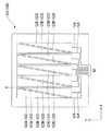
一方、対向基板12は、例えばガラスや石英、プラスチックなどの透光性材料で構成された基板本体41と、基板本体41の内側(液晶層13側)の表面に順次積層された遮光膜42、カラーフィルタ層43及び配向膜44とを備えている。また、対向基板12は、図3及び図4に示すように、基板本体41の外側の表面に形成された検出電極51、52と、引廻配線53及び端子部54と、検出電極51、52と、引廻配線53及び端子部54を被覆する被覆膜55とを備えている。 On the other hand, the
遮光膜42は、図3に示すように、基板本体41の表面のうち平面視でサブ画素領域の縁部であって液晶層13などを介してTFT素子22やデータ線23、走査線24と重なる領域に、平面視でほぼ格子状に形成されている。そして、遮光膜42は、サブ画素領域を縁取っている。
カラーフィルタ層43は、遮光膜42で区画された領域内であって各サブ画素領域に対応して配置されており、例えばアクリルなどで構成されて各サブ画素領域で表示する色に対応する色材を含有している。
配向膜44は、例えばポリイミドなどの透光性の樹脂材料で構成されており、遮光膜42及びカラーフィルタ層43を覆うように設けられている。そして、配向膜44の内側の表面には、配向処理が施されている。As shown in FIG. 3, the
The
The
検出電極51、52は、図4に示すように、画像表示領域と重なる検出領域A内において複数(本実施形態では検出電極51、52共に5つずつ)形成されており、例えばITO(酸化インジウムスズ)などの透光性導電材料で構成されている。そして、検出電極51、52は、平面視でほぼ矩形状の検出領域Aの一辺方向であるX軸方向(第1方向)に沿って形成されている。また、検出電極51と検出電極52とは、検出領域Aの他の一辺方向であってX軸方向と直交するY軸方向(第2方向)に沿って交互に配置されている。 As shown in FIG. 4, a plurality of
検出電極51、52は、検出電極51、52は、平面視でほぼ直角三角形状を有しており、その形状が同一となっている。
検出電極51は、直角を挟む2辺がそれぞれX軸方向、Y軸方向と平行となっており、その斜辺がX軸方向及びY軸方向から傾いてY軸方向の一方(+Y側)を向くように形成されている。そして、検出電極51は、X軸方向の一方(−X側)から他方(+X側)に向かうにしたがってその幅が漸次狭くなっている。
一方、検出電極52は、直角を挟む2辺がそれぞれX軸方向、Y軸方向と平行となっており、その斜辺がX軸方向及びY軸方向から傾いてY軸方向の他方(−Y側)を向くように形成されている。そして、検出電極52は、X軸方向の−X側から+X側に向かうにしたがってその幅が漸次広くなっている。
ここで、複数の検出電極51のうち、最も−Y側に配置されているものから順に検出電極51A〜51Eと称する。また、複数の検出電極52のうち、最も−Y側に配置されているものから順に検出電極52A〜52Eと称する。The
In the
On the other hand, two sides of the
Here, among the plurality of
また、ほぼ直角三角形状の検出電極51、52のうちY軸方向においてその斜辺が向かい合うように隣り合う2つの検出電極51、52は、検出電極対56を構成している。したがって、一対の検出電極対56は、一方の検出電極51の幅と他方の検出電極52の幅との比率が、X軸方向に沿って−X側から+X側に向かって変化している。すなわち、X軸方向に沿って−X側から+X側に向かって、検出電極対56における検出電極51の幅の比率が、漸次小さくなると共に、検出電極52の幅の比率が漸次大きくなっている。
そして、この検出電極対56の外形は、検出電極51、52の斜辺が向かい合っていることから、平面視でほぼ矩形状となっている。また、検出電極対56は、検出電極51、52がそれぞれ5つずつ形成されていることから5対形成されている。
ここで、5対の検出電極対56のうち、−Y側に位置している側から順に検出電極対56A〜56Eと称する。すなわち、検出電極51A、52Aにより検出電極対56Aが形成され、検出電極51B、52Bにより検出電極対56Bが形成され、検出電極51C、52Cにより検出電極対56Cが形成され、検出電極51D、52Dにより検出電極対56Dが形成され、検出電極51E、52Eにより検出電極対56Eが形成される。Further, of the
The outer shape of the
Here, among the five detection electrode pairs 56, the detection electrode pairs 56A to 56E are sequentially called from the side located on the −Y side. That is, the
なお、図5に示すように、平面視でほぼ矩形状の検出領域Aで検出可能なX軸方向の座標であるX座標及びY軸方向の座標であるY座標は、それぞれ0以上1以下、1以上5以下となっている。ここで、検出領域Aの−X側の端辺と対応するX座標の値が0、検出領域Aの+X側の端辺と対応するX座標の値が1と対応している。また、検出電極対56AのX軸方向と平行な中心線と対応するY座標の値が1、検出電極対56BのX軸方向と平行な中心線と対応するY座標の値が2、検出電極対56CのX軸方向と平行な中心線と対応するY座標の値が3、検出電極対56DのX軸方向と平行な中心線と対応するY座標の値が4、検出電極対56EのX軸方向と平行な中心線と対応するY座標の値が5となっている。 As shown in FIG. 5, the X coordinate that is the coordinate in the X-axis direction and the Y coordinate that is the coordinate in the Y-axis direction that can be detected in the detection region A that is substantially rectangular in plan view are 0 or more and 1 or less, respectively. It is 1 or more and 5 or less. Here, the X coordinate value corresponding to the −X side edge of the detection area A corresponds to 0, and the X coordinate value corresponding to the + X side edge of the detection area A corresponds to 1. Further, the Y coordinate value corresponding to the center line parallel to the X axis direction of the
引廻配線53は、図4に示すように、検出電極51、52と共に基板本体41の外側の表面であって対向基板12の外周に沿って形成されており、検出電極51、52と端子部54とを接続している。また、引廻配線53は、例えばAl(アルミニウム)などのITOと比較して抵抗率の小さい導電材料で構成されている。そして、検出電極51と接続される引廻配線53は、検出電極51の−X側の端部において検出電極51に接続されている。また、検出電極52と接続される引廻配線53は、検出電極52の+X側の端部において検出電極52に接続されている。
端子部54は、検出電極51、52や引廻配線53と共に基板本体41の外側の表面であって検出領域Aの−Y側の外部に形成されており、対向基板12の外部に設けられた検出手段17に接続されている。そして、端子部54を介して検出電極51、52に検出手段17からの交流電圧が印加される。As shown in FIG. 4, the
The
偏光板15は、図3に示すように、例えばPVA(ポリビニルアルコール)の絶縁材料を用いて形成されたフィルムを基体として構成されている。
偏光板16は、偏光板15と同様にPVAのフィルムを基体として構成されている。なお、偏光板16の外面側には、偏光板16を保護する保護フィルム(図示略)を設けてもよい。また、偏光板16は、その透過軸が偏光板15とほぼ直交するように設けられている。
ここで、偏光板16の内側には、1/4波長板を配置してもよい。1/4波長板を配置することで、偏光板16の外面から入射した外光が素子基板11で反射して再び射出することを防止できる。なお、1/4波長板に合わせて、偏光板16の透過軸を適宜変更する。
また、偏光板15、16の一方または双方の内側には、光学補償フィルム(図示略)を配置してもよい。光学補償フィルムを配置することで、表示装置1を斜視した場合の液晶層13の位相差を補償することができ、光漏れを減少させてコントラストを増加させることができる。光学補償フィルムとしては、負の一軸性媒体と正の一軸性媒体とを組み合わせたものや、各方向の屈折率がnx>nz>nyである二軸性媒体が用いられる。As shown in FIG. 3, the
Similarly to the
Here, a quarter wavelength plate may be disposed inside the
Further, an optical compensation film (not shown) may be disposed inside one or both of the
検出手段17は、図1に示すように、端子部54を介して検出電極51、52に交流電圧を印加し、偏光板16及び被覆膜55を介して検出電極51、52との間の静電容量を検出して指などを接触させていない基準状態において検出される電圧と、指などを接触させた状態において検出される電圧との差を静電容量の変化量として検出する構成となっている。
算出手段18は、検出手段17による各検出電極51、52の静電容量の変化量からX軸方向における座標を算出するX座標算出手段(第1座標算出手段)18Aと、Y軸方向における座標を算出するY軸座標算出手段(第2座標算出手段)18Bとを備えている。なお、算出手段18による座標の算出方法については、後述する。
これら対向基板12、偏光板16、検出手段17及び算出手段18により、座標入力装置57が構成される。As shown in FIG. 1, the detection means 17 applies an AC voltage to the
The calculation means 18 includes an X coordinate calculation means (first coordinate calculation means) 18A for calculating coordinates in the X axis direction from the amount of change in capacitance of each
The
〔表示装置の動作〕
次に、以上のような構成の表示装置1の動作について説明する。素子基板11の外面側から入射した光は、偏光板15によって直線偏光に変換されて液晶層13に入射する。
ここで、画素電極21と共通電極36との間に電圧が印加されていないオフ状態の場合であれば、液晶層13に入射した直線偏光は、液晶層13により入射時と同一の偏光状態で液晶層13から射出する。そして、この直線偏光は、その偏光方向が偏光板16の透過軸と直交するため、偏光板16で遮断され、サブ画素領域が暗表示となる。
一方、画素電極21と共通電極36との間に電圧が印加されているオン状態の場合であれば、液晶層13に入射した直線偏光は、液晶層13により所定の位相差(1/2波長分)の位相差が付与され、入射時の偏光方向と直交する直線偏光に変換されて液晶層13から射出する。そして、この直線偏光は、その偏光方向が偏光板16の透過軸と平行であるため、偏光板16を透過して表示光として視認され、サブ画素領域が明表示となる。[Operation of display device]
Next, the operation of the
Here, in the case of an off state in which no voltage is applied between the
On the other hand, when the voltage is applied between the
そして、検出電極51、52に交流電圧を印加した状態で偏光板16に人間の指などが触れると、偏光板16及び被覆膜55を介して検出電極51、52と指などとの間で静電容量が形成される。そのため、検出電極51、52から静電容量を介して電流が流れる。検出手段17は、静電容量が形成されることによって電流の変化量を静電容量の変化量として検出する。そして、算出手段18は、検出手段17において検出された静電容量の変化量から、検出領域Aにおける指などの接触位置を算出する。
その後、算出した接触位置の情報に基づいて、画像表示領域に表示される画像を切り替えたり、偏光板16の表面で移動する指の軌跡を画像表示領域に画像として表示させたりする。When an alternating voltage is applied to the
Thereafter, based on the calculated contact position information, the image displayed in the image display area is switched, or the locus of the finger moving on the surface of the
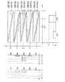
ここで、接触位置の算出方法について具体的に説明する。なお、図5は接触位置の算出方法を示す説明図、図6は接触位置の算出方法を示すフローチャートである。また、図5に示す符号Tは、偏光板16に対する指の接触領域を示している。
まず、検出手段17は、各検出電極51、52における静電容量の変化量CL、CRを検出する(図6に示すステップST1)。ここでは、検出手段17が、指などを接触させていない基準状態において各検出電極51、52で検出される静電容量と、指などを接触させた状態において各検出電極51、52で検出される静電容量との差を検出する。Here, the calculation method of a contact position is demonstrated concretely. 5 is an explanatory diagram showing a method for calculating the contact position, and FIG. 6 is a flowchart showing the method for calculating the contact position. 5 indicates a contact area of the finger with respect to the
First, the detection means 17 detects the capacitance changes CL and CR in the
また、X座標算出手段18Aは、各検出電極51で検出した静電容量の変化量CLの和であるΣCLを算出すると共に(図6に示すステップST2)、各検出電極52で検出した静電容量の変化量CRの和であるΣCRを算出する(図6に示すステップST3)。そして、X座標算出手段18Aは、ΣCLとΣCRとの比を計算し(図6に示すステップST4)、X座標を算出する(図6に示すステップST5)。
したがって、例えば図5に示すように、ΣCLとΣCRとの比が1:3である場合、ΣCLと(ΣCL+ΣCR)との比が1:4であることから、X座標算出手段18Aは、X座標の値を0.75として算出する。Further, the X-coordinate calculating means 18A calculates ΣCL, which is the sum of the capacitance variation CL detected by each detection electrode 51 (step ST2 shown in FIG. 6), and the electrostatic capacitance detected by each
Therefore, for example, as shown in FIG. 5, when the ratio of ΣCL to ΣCR is 1: 3, the ratio of ΣCL to (ΣCL + ΣCR) is 1: 4. Is calculated as 0.75.
一方、Y座標算出手段18Bは、各検出電極対56A〜56Eにおける静電容量の変化量CPを算出する(図6に示すステップST6)。そして、検出電極対56A〜56Eにおける静電容量の変化の重心位置を算出するセントロイド計算を行う(図6に示すステップST7)。ここでは、下記の式(1)を用いてY座標を算出する(図6に示すステップST8)。
y=Σ(n×CP)/ΣCP…式(1)
ここで、n×CPは、検出電極対56における静電容量の変化量CPと、その検出電極対56の幅方向の中心線と対応するY座標の値との積を示している。
したがって、例えば図5に示すように、検出電極対56Aにおける静電容量の変化量CP1を0、検出電極対56Bにおける静電容量の変化量CP2を1、検出電極対56Bにおける静電容量の変化量CP3を4、検出電極対56Dにおける静電容量の変化量CP4を3、検出電極対56Bにおける静電容量の変化量CP5を0とする。このとき、(1×0+2×1+3×4+4×2+5×0)/(0+1+4+2+0)=3.14となる。よって、Y座標算出手段18Bは、Y座標の値を3.14として算出する。
以上のようにして、X座標及びY座標の値から指の接触位置を算出する。On the other hand, the Y coordinate calculation means 18B calculates the change amount CP of the electrostatic capacitance in each of the detection electrode pairs 56A to 56E (step ST6 shown in FIG. 6). Then, centroid calculation is performed to calculate the gravity center position of the capacitance change in the detection electrode pairs 56A to 56E (step ST7 shown in FIG. 6). Here, the Y coordinate is calculated using the following equation (1) (step ST8 shown in FIG. 6).
y = Σ (n × CP) / ΣCP (1)
Here, n × CP represents the product of the capacitance variation CP of the
Therefore, for example, as shown in FIG. 5, the capacitance variation CP1 in the
As described above, the contact position of the finger is calculated from the values of the X coordinate and the Y coordinate.
〔電子機器〕
以上のような構成の表示装置1は、例えば図7に示すようなPDA100の表示部101として用いられる。また、PDA100には、電源入力スイッチなどのスイッチが適宜設けられている。〔Electronics〕
The
以上のように、本実施形態における座標入力装置57及びこれを備える表示装置1によれば、検出電極51、52と引廻配線53と端子部54とを同層上に形成できるので、製造工程の簡略化及び製造コストの削減が図れる。
また、検出電極51、52を対向基板12のうち液晶層13から離間した外面側に設けることで、偏光板16に指などが接触した際の接触位置の高い検出精度が得られる。As described above, according to the coordinate
Further, by providing the
[第2の実施形態]
次に、本発明における座標入力装置及び表示装置の第2の実施形態を、図面に基づいて説明する。ここで、図8は接触位置の算出方法を示す説明図、図9は接触位置の算出方法を示すフローチャートである。なお、本実施形態では、第1の実施形態と静電容量の検出位置の算出方法が異なるため、この点を中心に説明すると共に、上記実施形態で説明した構成要素には同一符号を付し、その説明を省略する。[Second Embodiment]
Next, a second embodiment of the coordinate input device and the display device according to the present invention will be described with reference to the drawings. Here, FIG. 8 is an explanatory view showing a calculation method of the contact position, and FIG. 9 is a flowchart showing the calculation method of the contact position. In this embodiment, since the calculation method of the capacitance detection position is different from that in the first embodiment, this point will be mainly described, and the same reference numerals are given to the components described in the above embodiment. The description is omitted.
〔表示装置〕
本実施形態における表示装置では、図8に示すように、検出電極対56を構成する一方の検出電極51と、この検出電極51と隣接する他の検出電極対56を構成する他方の検出電極52とにより、補正検出電極対110が構成されている。この補正検出電極対110の外形は、検出電極51、52のX軸方向に延在する辺が向かい合うように配置されていることから、平面視でほぼ平行四辺形状となっている。そして、補正検出電極対110は、4対形成されている。
ここで、4対の補正検出電極対110のうち、最も−Y側に位置しているものから順に、補正検出電極対110A〜110Dと称する。すなわち、検出電極51B、52Aにより補正検出電極対110Aが形成され、検出電極51C、52Bにより補正検出電極対110Bが形成され、検出電極51D、52Cにより補正検出電極対110Cが形成され、検出電極51E、52Dにより補正検出電極対110Dが形成される。[Display device]
In the display device according to the present embodiment, as shown in FIG. 8, one
Here, of the four pairs of correction detection electrode pairs 110, the correction detection electrode pairs 110A to 110D are referred to in order from the one located closest to the −Y side. That is, the
〔表示装置の動作〕
まず、検出手段17は、上述した第1の実施形態と同様に、各検出電極51、52における静電容量の変化量CL、CRを検出する(図9に示すステップST1)。
そして、X座標算出手段18Aは、上述した第1の実施形態と同様に、X座標を算出する(図9に示すステップST2〜ST5)。
したがって、例えば図8に示すように、ΣCLとΣCRとの比が1:3である場合、X座標算出手段18Aは、0.75の地点をX座標として算出する。[Operation of display device]
First, the detection means 17 detects the capacitance changes CL and CR of the
And X coordinate calculation means 18A calculates X coordinate similarly to 1st Embodiment mentioned above (steps ST2-ST5 shown in FIG. 9).
Therefore, for example, as shown in FIG. 8, when the ratio of ΣCL to ΣCR is 1: 3, the X coordinate calculation means 18A calculates the point of 0.75 as the X coordinate.
そして、Y座標算出手段18Bは、上述した第1の実施形態と同様に、各検出電極対56A〜56Eにおける静電容量の変化量CPを算出する(図9に示すステップST10)。
また、Y座標算出手段18Bは、補正検出電極対110A〜110Dにおける静電容量の変化量CP’を算出する(図9に示すステップST11)。ここで、補正検出電極対110は、平面視で平行四辺形状となっており、その中心軸がX軸方向に対して傾斜している。そのため、CP’を用いてセントロイド計算をする際、計算式をX座標の値に応じて適宜変更する必要がある。そこで、Y座標算出手段18Bは、X座標の値に応じてセントロイド計算に用いる計算式の補正を行う(図9に示すステップST12)。Then, the Y-coordinate calculating
Further, the Y coordinate calculation means 18B calculates the change amount CP ′ of the capacitance in the correction detection electrode pairs 110A to 110D (step ST11 shown in FIG. 9). Here, the correction
例えば補正検出電極対110Aでは、図10に示すように、X座標の値が0であるときの幅方向の中心線と対応するY座標の値が2であって、X座標の値が1であるときの幅方向の中心線と対応するY座標の値が1である。そのため、X座標の値がxであるときの幅方向の中心線と対応するY座標の値は、(2−x)となる。同様に、X座標の値がxであるときの幅方向の中心線と対応するY座標の値は、補正検出電極対110Bで(3−x)、補正検出電極対110Cで(4−x)、補正検出電極対110Dで(5−x)となる。
したがって、X座標の値が0.75である場合には、それぞれの値が、1.25、2.25、3.25、4.25となる。For example, in the correction
Therefore, when the value of the X coordinate is 0.75, the respective values are 1.25, 2.25, 3.25, and 4.25.
そして、Y座標算出手段18Bは、CP及びCP’を用いて静電容量の変化の重心位置を算出するセントロイド計算を行う(図9に示すステップST13)。ここでは、下記の式(2)を用いてY軸方向におけるY座標を算出する(図9に示すステップST14)。
y=(Σ(n×CP)+Σ(n’×CP’))/(ΣCP+ΣCP’)…式(2)
ここで、n×CPは、検出電極対56における静電容量の変化量CPと、その検出電極対56の幅方向の中心線と対応するY座標の値との積を示している。また、n’×CP’は、補正検出電極対110における静電容量の変化量CP’と、この補正検出電極対110のX座標の値がxである際の幅方向の中心線と対応するY座標の値との積を示している。
したがって、例えば図8に示すように、変化量CP1を0、変化量CP2を1、変化量CP3を4、変化量CP4を3、変化量CP5を0とする。また、補正検出電極対110Aにおける静電容量の変化量CP’1を0、補正検出電極対110Bにおける静電容量の変化量CP’2を1、補正検出電極対110Cにおける静電容量の変化量CP’3を3.5、補正検出電極対110Dにおける静電容量の変化量CP’4を0.5とする。このとき、((1×0+2×1+3×4+4×2+5×0)+(1.25×0+2.25×1+3.25×3.5+4.25×1))/((0+1+4+2+0)+(0+1+3.5+0.5))=3.15となる。よって、Y座標算出手段18Bは、3.15の地点をY座標として算出する。
以上のようにして、X座標及びY座標の値から指の接触位置を算出する。Then, the Y coordinate calculation means 18B performs centroid calculation for calculating the gravity center position of the change in capacitance using CP and CP ′ (step ST13 shown in FIG. 9). Here, the Y coordinate in the Y-axis direction is calculated using the following equation (2) (step ST14 shown in FIG. 9).
y = (Σ (n × CP) + Σ (n ′ × CP ′)) / (ΣCP + ΣCP ′) (2)
Here, n × CP represents the product of the capacitance variation CP of the
Therefore, for example, as shown in FIG. 8, the variation CP1 is 0, the variation CP2 is 1, the variation CP3 is 4, the variation CP4 is 3, and the variation CP5 is 0. In addition, the capacitance variation CP′1 in the correction
As described above, the contact position of the finger is calculated from the values of the X coordinate and the Y coordinate.
以上のような構成の座標入力装置及びこれを備える表示装置においても、上述した第1の実施形態と同様の作用、効果を奏するが、補正検出電極対110により算出された静電容量の変化量も用いてY座標を算出するので、検出精度が向上する。ここで、補正検出電極対110の中心線のX軸方向に対する傾きを考慮してセントロイド計算の補正を行っているため、Y座標の算出精度がより向上する。 The coordinate input device having the above-described configuration and the display device including the same also have the same operations and effects as those of the first embodiment described above, but the amount of change in capacitance calculated by the correction
[第3の実施形態]
次に、本発明における座標入力装置及び表示装置の第3の実施形態を、図面に基づいて説明する。ここで、図11は接触位置の算出方法を示す説明図、図12は接触位置の算出方法を示すフローチャートである。[Third Embodiment]
Next, a third embodiment of the coordinate input device and the display device according to the present invention will be described with reference to the drawings. Here, FIG. 11 is an explanatory diagram showing a method for calculating the contact position, and FIG. 12 is a flowchart showing the method for calculating the contact position.
次に、以上のような構成の表示装置による接触位置の算出方法について説明する。
まず、検出手段17は、上述した第1の実施形態と同様に、各検出電極51、52における静電容量の変化量CL、CRを検出する(図12に示すステップST1)。
そして、X座標算出手段18Aは、上述した第1の実施形態と同様に、X座標を算出する(図12に示すステップST2〜ST5)。Next, a method for calculating the contact position by the display device having the above configuration will be described.
First, the detection means 17 detects the capacitance changes CL and CR of the
And X coordinate calculation means 18A calculates X coordinate similarly to 1st Embodiment mentioned above (steps ST2-ST5 shown in FIG. 12).
そして、Y座標算出手段18Bは、検出電極51A〜51Eにおける静電容量の変化の重心位置を算出するセントロイド計算を行う(図12に示すステップST20)。ここでは、下記の式(3)を用いて第1Y座標y1を算出する。
y1=Σ(n×CL)/ΣCL…式(3)
ここで、n×CLは、検出電極51における静電容量の変化量CLと、その検出電極51が形成する検出電極対56の幅方向の中心線と対応するY座標の値との積を示している。
したがって、例えば図11に示すように、検出電極51Aにおける静電容量の変化量CL1を0、検出電極51Bにおける静電容量の変化量CL2を0、検出電極51Cにおける静電容量の変化量CL3を1、検出電極51Dにおける静電容量の変化量CL4を1、検出電極51Eにおける静電容量の変化量CL5を0とする。このとき、(1×0+2×0+3×1+4×1+5×0)/(0+0+1+1+0)=3.5となる。よって、Y座標算出手段18Bは、y1を3.5として算出する。And the Y coordinate calculation means 18B performs the centroid calculation which calculates the gravity center position of the electrostatic capacitance change in the
y1 = Σ (n × CL) / ΣCL (3)
Here, n × CL indicates the product of the capacitance change amount CL of the
Therefore, for example, as shown in FIG. 11, the capacitance variation CL1 in the
さらに、Y座標算出手段18Bは、検出電極52A〜52Eにおける静電容量の変化の重心位置を算出するセントロイド計算を行う(図12に示すステップST21)。ここでは、下記の式(4)を用いて第2Y座標y2を算出する。
y2=Σ(n×CR)/ΣCR…式(4)
ここで、n×CRは、検出電極52における静電容量の変化量CRと、その検出電極52が形成する検出電極対56の幅方向の中心線と対応するY座標の値との積を示している。
したがって、例えば図11に示すように、検出電極52Aにおける静電容量の変化量CR1を0、検出電極52Bにおける静電容量の変化量CR2を0.4、検出電極52Cにおける静電容量の変化量CR3を3、検出電極52Dにおける静電容量の変化量CR4を0.5、検出電極52Eにおける静電容量の変化量CR5を0とする。このとき、(1×0+2×0.4+3×3+4×0.5+5×0)/(0+0.4+3+0.5+0)=3.03となる。よって、Y座標算出手段18Bは、y2を3.03として算出する。Further, the Y coordinate calculation means 18B performs centroid calculation for calculating the gravity center position of the capacitance change in the
y2 = Σ (n × CR) / ΣCR Equation (4)
Here, n × CR represents the product of the capacitance change amount CR in the
Therefore, for example, as shown in FIG. 11, the change amount CR1 of the capacitance in the
次に、Y座標算出手段18Bは、第1及び第2Y座標y1、y2の平均値を算出する(図12に示すステップST22)。そして、Y座標算出手段18Bは、その平均値をY座標として算出する(図12に示すステップST23)。
したがって、例えばy1が3.5、y2が3.03である場合には、その平均値が3.26となる。よって、Y座標算出手段18Bは、Y座標の値を3.26として算出する。 以上のようにして、X座標及びY座標の値から指の接触位置を算出する。Next, the Y coordinate calculation means 18B calculates the average value of the first and second Y coordinates y1, y2 (step ST22 shown in FIG. 12). And the Y coordinate calculation means 18B calculates the average value as a Y coordinate (step ST23 shown in FIG. 12).
Therefore, for example, when y1 is 3.5 and y2 is 3.03, the average value is 3.26. Therefore, the Y coordinate calculation means 18B calculates the value of the Y coordinate as 3.26. As described above, the contact position of the finger is calculated from the values of the X coordinate and the Y coordinate.
以上のような構成の座標入力装置及びこれを備える表示装置においても、上述した第1の実施形態と同様の作用、効果を奏する。 The coordinate input device configured as described above and the display device including the coordinate input device also have the same operations and effects as the first embodiment described above.
なお、本実施形態においては、以下のようにしてY座標の算出を行ってもよい。すなわち、検出電極51、52は、共に平面視でほぼ直角三角形状となっているため、その中心軸がX軸方向に対して傾斜している。
例えば検出電極51Aでは、図13に示すように、X座標の値が0であるときの幅方向の中心線と対応するY座標の値が1であって、X座標の値が1であるときの幅方向の中心線と対応するY座標の値が0.5である。そのため、X座標の値がxであるときの幅方向の中心線と対応するY座標の値は、(1−x/2)となる。そして、検出電極51Aが形成する検出電極対56Aの幅方向の中心線と対応するY座標の値が1であることから、X座標の値がxであるときの幅方向の中心線と対応するY座標の値との差は、(−x/2)となる。In the present embodiment, the Y coordinate may be calculated as follows. That is, since both the
For example, in the
一方、例えば検出電極52Aでは、X座標の値が0であるときの幅方向の中心線と対応するY座標の値が1.5であって、X座標の値が1であるときの幅方向の中心線と対応するY座標の値が1である。そのため、X座標の値がxであるときの幅方向の中心線と対応するY座標の値は、(1.5−x/2)となる。そして、検出電極52Aが形成する検出電極対56Aの幅方向の中心線と対応するY座標の値が1であることから、X座標の値がxであるときの幅方向の中心線と対応するY座標の値との差は、(0.5−x/2)となる。 On the other hand, for example, in the
そこで、Y座標算出手段18Bは、第1Y座標y1をセントロイド計算により算出した後(図14に示すステップST20)、第1Y座標y1に対して(−x/2)を加える(図14に示すステップST25)。また、第2Y座標y2をセントロイド計算により算出した後(図14に示すステップST21)、第2Y座標に対して(0.5−x/2)を加える補正を行って補正後の第1及び第2Y座標y1’、y2’を算出する(図14に示すステップST26)。
したがって、例えばy1が3.5、y2が3.03である場合には、y1’が3.13、y2’が3.15となる。よって、Y座標算出手段18Bは、Y座標の値を3.14として算出する。
このように、検出電極51、52の中心線のX軸方向に対する傾きに応じて算出したY座標の値を補正することで、中心線がX方向に対して傾いていることによる誤差の影響を抑制できる。Therefore, the Y coordinate calculation means 18B calculates the first Y coordinate y1 by centroid calculation (step ST20 shown in FIG. 14), and then adds (−x / 2) to the first Y coordinate y1 (shown in FIG. 14). Step ST25). Further, after the second Y coordinate y2 is calculated by centroid calculation (step ST21 shown in FIG. 14), the correction is performed by adding (0.5−x / 2) to the second Y coordinate, and the corrected first and second coordinates are corrected. Second Y coordinates y1 ′ and y2 ′ are calculated (step ST26 shown in FIG. 14).
Therefore, for example, when y1 is 3.5 and y2 is 3.03, y1 ′ is 3.13 and y2 ′ is 3.15. Therefore, the Y coordinate calculation means 18B calculates the value of the Y coordinate as 3.14.
Thus, by correcting the value of the Y coordinate calculated according to the inclination of the center line of the
また、本実施形態においては、以下のようにしてY座標の算出を行ってもよい。すなわち、上述したように、検出電極51、52は、共に平面視でほぼ直角三角形状となっている。そのため、検出電極51の幅が+X側に向かうにしたがって狭くなっていると共に、検出電極52の幅が+X側に向かうにしたがって広くなっている。ここで、静電容量の形成位置の検出精度は、静電容量の形成位置における検出電極51、52の面積が広いほど向上する。
そこで、Y座標算出手段18Bは、以下の式(5)を用いて、求めた第1及び第2Y座標y1、y2に対してX座標の値に応じて重み付けした平均値をY座標の値として算出する(図15に示すステップST27、ST23)。
y=(1−x)×y1+x×y2…式(5)
したがって、例えばX座標の値が0.75、y1が3.5、y2が3.03である場合には、(1−0.75)×3.5+0.75×3.03=3.14となる。よって、Y座標算出手段18Bは、Y座標の値を3.14として算出する。
このように、X座標の値を用いて重み付けすることで、静電容量の形成位置における検出電極51、52の面積に応じた検出精度の誤差の影響を抑制できる。In the present embodiment, the Y coordinate may be calculated as follows. That is, as described above, the
Therefore, the Y coordinate calculation means 18B uses the following equation (5) as an average value obtained by weighting the obtained first and second Y coordinates y1, y2 according to the value of the X coordinate as the value of the Y coordinate. Calculate (steps ST27 and ST23 shown in FIG. 15).
y = (1-x) * y1 + x * y2 ... Formula (5)
Therefore, for example, when the value of the X coordinate is 0.75, y1 is 3.5, and y2 is 3.03, (1−0.75) × 3.5 + 0.75 × 3.03 = 3.14. It becomes. Therefore, the Y coordinate calculation means 18B calculates the value of the Y coordinate as 3.14.
Thus, by weighting using the value of the X coordinate, it is possible to suppress the influence of an error in detection accuracy according to the areas of the
[第4の実施形態]
次に、本発明における座標入力装置及び表示装置の第4の実施形態を、図面に基づいて説明する。ここで、図16は表示装置を示す概略構成図である。なお、本実施形態では検出電極の配置が異なるため、この点を中心に説明すると共に、上記実施形態で説明した構成要素には同一符号を付し、その説明を省略する。[Fourth Embodiment]
Next, a coordinate input device and a display device according to a fourth embodiment of the present invention will be described with reference to the drawings. Here, FIG. 16 is a schematic configuration diagram showing the display device. In this embodiment, since the arrangement of the detection electrodes is different, this point will be mainly described, and the constituent elements described in the above embodiment will be denoted by the same reference numerals and description thereof will be omitted.
本実施形態における表示装置120は、図16に示すように、対向基板121に設けられた検出電極122、123が検出領域Aの一辺方向であるY軸方向(第1方向)に沿って形成されている。そして、検出電極122、123は、X軸方向(第2方向)に沿って交互に配置されている。
引廻配線124は、検出電極122、123の−Y側の端部に接続されており、検出電極122、123を構成するITOなどの透光性導電材料で構成されている。このように、引廻配線124を検出電極122、123のうち端子部54に近接している−Y側の端部に接続することで、引廻配線124による引き廻し長さが短くなる。
また、端子部54は、引廻配線124と同様に、検出電極122、123を構成するITOなどの透光性導電材料で構成されている。In the
The
The
以上のような構成の座標入力装置及び表示装置120によれば、引廻配線124による引き廻し長さを短くすることで、引廻配線124及び端子部54をITOなどの透光性導電材料で形成した場合であっても引廻配線124における抵抗値を抑制できる。このように引廻配線124及び端子部54と検出電極122、123とを同一材料で構成することで、引廻配線124と検出電極122、123とを同一工程で形成でき、製造工程のさらなる簡略化及び製造コストのさらなる低減化が図れる。
なお、本実施形態における検出電極122、123及び引廻配線124の構成は、上述した第2実施形態や第3実施形態に適用されてもよい。According to the coordinate input device and the
Note that the configurations of the
[第5の実施形態]
次に、本発明における座標入力装置及び表示装置の第5の実施形態を、図面に基づいて説明する。ここで、図17は表示装置を示す概略構成図である。なお、本実施形態では検出電極の配置が異なるため、この点を中心に説明すると共に、上記実施形態で説明した構成要素には同一符号を付し、その説明を省略する。[Fifth Embodiment]
Next, a fifth embodiment of a coordinate input device and a display device according to the present invention will be described with reference to the drawings. Here, FIG. 17 is a schematic configuration diagram showing the display device. In this embodiment, since the arrangement of the detection electrodes is different, this point will be mainly described, and the constituent elements described in the above embodiment will be denoted by the same reference numerals and description thereof will be omitted.
本実施形態における表示装置130は、図17に示すように、対向基板131を構成する基板本体41の内側の表面に検出電極51、52が形成されている。
すなわち、基板本体41の内側の表面には、検出電極51、52、引廻配線53(図17では図示略)及び端子部54(図17では図示略)が形成されている。そして、これら検出電極51、52、引廻配線53及び端子部54が被覆膜55により被覆されている。
遮光膜42及びカラーフィルタ層43は、被覆膜55の内側の表面に形成されている。In the
That is, on the inner surface of the
The
以上のような構成の座標入力装置及び表示装置130によれば、対向基板131の内側の面に検出電極51、52や遮光膜42及びカラーフィルタ層43などの各部材を形成するため、製造工程の簡略化が図れる。
なお、本実施形態における対向基板131の構成は、上述した第2から第4の実施形態に適用されてもよい。According to the coordinate input device and
Note that the configuration of the
なお、本発明は上記実施形態に限定されるものではなく、本発明の趣旨を逸脱しない範囲において種々の変更を加えることが可能である。
例えば、検出電極の外形は、ほぼ直角三角形状となっているが、他方の検出電極との間でX軸方向における幅の比率が変化すれば、他の形状であってもよい。すなわち、検出電極の外形は、一対の側辺の一方をX軸方向と平行にすると共に底辺をY軸方向と平行にした台形状であってもよい。また、検出電極の外形は、二等辺三角形状など一対の側辺がX軸から傾けた形状であってもよい。そして、検出電極の外形は、一対の側辺が直線状でなくてもよい。
また、一対の検出電極対を構成する各検出電極を合同とすることにより同一形状としているが、同一形状でなくてもよい。In addition, this invention is not limited to the said embodiment, A various change can be added in the range which does not deviate from the meaning of this invention.
For example, the outer shape of the detection electrode is substantially a right triangle, but may be another shape as long as the ratio of the width in the X-axis direction changes with the other detection electrode. That is, the outer shape of the detection electrode may be trapezoidal in which one of the pair of side sides is parallel to the X-axis direction and the bottom side is parallel to the Y-axis direction. Further, the outer shape of the detection electrode may be a shape in which a pair of side sides is inclined from the X axis, such as an isosceles triangle shape. And as for the external shape of a detection electrode, a pair of side may not be linear.
Moreover, although it is set as the same shape by making each detection electrode which comprises a pair of detection electrode pair congruent, it does not need to be the same shape.
また、静電容量の形成位置を算出できれば、互いに直交するXY座標系に限らず、検出領域内で互いに交差する2方向における座標を算出する構成としてもよい。
そして、算出手段は、上述した第1から第3の実施形態における算出方法に限らず、他の方法によって静電容量の形成位置を算出する構成としてもよい。
さらに、表示装置の画素電極及び共通電極の電極構造をFFS構造としているが、IPS構造など、他の電極構造であってもよい。Further, as long as the electrostatic capacitance formation position can be calculated, the coordinates in two directions intersecting each other in the detection region may be calculated without being limited to the XY coordinate system orthogonal to each other.
The calculation means is not limited to the calculation methods in the first to third embodiments described above, and may be configured to calculate the capacitance formation position by another method.
Furthermore, although the electrode structure of the pixel electrode and the common electrode of the display device is an FFS structure, other electrode structures such as an IPS structure may be used.
また、表示装置を備える電子機器としては、PDAに限らず、携帯電話機やハンディターミナル、電子ブック、ノート型パーソナルコンピュータ、パーソナルコンピュータ、デジタルスチルカメラ、液晶テレビ、ビューファインダ型あるいはモニタ直視型のビデオテープレコーダ、カーナビゲーション装置、ページャ、電子手帳、電卓、ワードプロセッサ、ワークステーション、テレビ電話、POS端末など、種々の電子機器であってもよい。
そして、表示装置は、液晶表示装置を構成しているが、有機EL表示装置や電気泳動表示装置など、他の表示装置を構成してもよい。
ここで、座標入力装置を液晶表示装置に組み込んでいるが、液晶表示装置に組み込まずに座標入力装置単独の構成としてもよい。In addition, the electronic device including the display device is not limited to the PDA, but is a mobile phone, a handy terminal, an electronic book, a notebook personal computer, a personal computer, a digital still camera, a liquid crystal television, a viewfinder type, or a monitor direct view type video tape. Various electronic devices such as a recorder, a car navigation device, a pager, an electronic notebook, a calculator, a word processor, a workstation, a videophone, and a POS terminal may be used.
The display device constitutes a liquid crystal display device, but other display devices such as an organic EL display device and an electrophoretic display device may be constituted.
Here, although the coordinate input device is incorporated in the liquid crystal display device, the coordinate input device alone may be configured without being incorporated in the liquid crystal display device.
1,120,130 表示装置、11 素子基板(基板)、12,121,131 対向基板(他の基板)、13 液晶層(電気光学層)、17 検出手段、18 算出手段、18A X座標算出手段(第1座標算出手段)、18B Y座標算出手段(第2座標算出手段)、51,51A〜51E,122 検出電極(一方の検出電極)、52,52A〜52E,123 検出電極(他方の検出電極)、53,124 引廻配線、55 被覆膜、56,56A〜56E 検出電極対、57 座標入力装置、100 PDA(電子機器)、110,110A〜110D 補正検出電極対、A 検出領域1,120,130 display device, 11 element substrate (substrate), 12, 121, 131 counter substrate (other substrate), 13 liquid crystal layer (electro-optic layer), 17 detection means, 18 calculation means, 18A X coordinate calculation means (First coordinate calculation means), 18BY coordinate calculation means (second coordinate calculation means), 51, 51A to 51E, 122 detection electrode (one detection electrode), 52, 52A to 52E, 123 detection electrode (the other detection) Electrode), 53,124 lead wiring, 55 coating film, 56, 56A to 56E detection electrode pair, 57 coordinate input device, 100 PDA (electronic device), 110, 110A to 110D correction detection electrode pair, A detection area
Claims (6)
Translated fromJapanese該複数の検出電極のそれぞれに接続された複数の引廻配線と、
前記複数の検出電極を被覆する被覆膜と、
該被覆膜を介して前記複数の検出電極と被検出物との間に形成される静電容量の変化を検出する検出手段と、
該検出手段の検出結果から前記静電容量の形成位置を算出する算出手段とを備え、
前記複数の検出電極が、前記検出領域内の第1方向に沿って形成されると共に、該第1方向と交差する第2方向に沿って配列され、隣り合う一対の前記検出電極により検出電極対を複数構成し、
該検出電極対を構成する前記一対の検出電極の一方の検出電極の幅と他方の検出電極の幅との比率が、前記第1方向に沿って変化し、
前記複数の引廻配線のそれぞれが、前記検出電極のうち前記第1方向のいずれかの端部に接続されると共に、前記複数の検出電極と同層上に形成されており、
前記複数の検出電極の外形が、それぞれ合同であり、前記検出電極対を構成する前記一方の検出電極の幅が、前記第1方向で一方から他方に向かうにしたがって小さくなり、前記他方の検出電極の幅が、前記第1方向で前記一方から他方に向かうにしたがって大きくなっており、
前記複数の検出電極は、それぞれ前記第1方向に沿う一対の側辺が、直線状であり、
前記複数の検出電極が、前記検出電極対を構成する前記一方の検出電極と該一方の検出電極と隣り合う他の前記検出電極対を構成する前記他方の検出電極とにより補正検出電極対を構成し、
前記算出手段が、前記一方の検出電極での前記静電容量の変化量の和と、前記他方の検出電極での前記静電容量の変化量の和とに基づいて、前記第1方向での前記検出位置である第1座標を算出する第1座標算出手段と、
前記各検出電極対での前記静電容量の変化量と、前記一方の検出電極及び該一方の検出電極と隣り合う他の前記検出電極対を構成する前記他方の検出電極での前記静電容量の変化量と、前記第1座標とから、前記第2方向での前記検出位置である第2座標を算出する第2座標算出手段とを備え、
前記第2座標算出手段は、前記検出電極対の幅方向の中心線に対する前記補正検出電極対の幅方向の中心線の傾きに基づいて補正した前記第1座標を用いて前記第2座標を算出することを特徴とする座標入力装置。A plurality of detection electrodes arranged in a plane within a detection region on the substrate;
A plurality of lead wires connected to each of the plurality of detection electrodes;
A coating film covering the plurality of detection electrodes;
Detection means for detecting a change in capacitance formed between the plurality of detection electrodes and thedetection object via the coating film;
Calculation means for calculating the formation position of the capacitance from the detection result of the detection means,
The plurality of detection electrodes are formed along a first direction in the detection region and arranged along a second direction that intersects the first direction, and a pair of adjacent detection electrodes forms a detection electrode pair. Multiple
The ratio of the width of the otherdetection electrodes on oneof the detection electrodes of the pair of detection electrodes constituting the detection electrode pair varies along the first direction,
Each of the plurality of lead wirings is connected to one end of the detection electrode in the first direction and is formed on the same layer as the plurality of detection electrodes.
The external shapes of the plurality of detection electrodes are respectively congruent, and the width of the one detection electrode constituting the detection electrode pair decreases from one to the other in the first direction, and the other detection electrode The width increases in the first direction from the one to the other,
Each of the plurality of detection electrodes has a pair of side sides along the first direction, and is linear.
The plurality of detection electrodes constitute a correction detection electrode pair by the one detection electrode constituting the detection electrode pair and the other detection electrode constituting the other detection electrode pair adjacent to the one detection electrode. And
The calculating means is configured to calculate the first direction based on the sum of the amount of change in the capacitance at the one detection electrode and the sum of the amount of change in the capacitance at the other detection electrode. First coordinate calculation means for calculating the first coordinate as the detection position;
The amount of change in capacitance at each detection electrode pair, and the capacitance at the other detection electrode constituting the one detection electrode and the other detection electrode pair adjacent to the one detection electrode A second coordinate calculation means for calculating a second coordinate that is the detection position in the second direction from the change amount of the first coordinate and the first coordinate;
The second coordinate calculation means calculates the second coordinate using the first coordinate corrected based on the inclination of the center line in the width direction of the corrected detection electrode pair with respect to the center line in the width direction of the detection electrode pair. A coordinate input device characterized by:
前記検出電極対を構成する前記一対の検出電極は、前記他方の側辺が対向配置されていることを特徴とする請求項1に記載の座標入力装置。One of the pair of side sides is parallel to the first direction, and the other is inclined from the first and second directions,
The coordinate input device according to claim 1, wherein the other side of the pair of detection electrodes constituting the detection electrode pair is disposed opposite to the other.
Priority Applications (4)
| Application Number | Priority Date | Filing Date | Title |
|---|---|---|---|
| JP2007111480AJP4967780B2 (en) | 2007-04-20 | 2007-04-20 | Coordinate input device and display device |
| US12/051,175US8159471B2 (en) | 2007-04-20 | 2008-03-19 | Coordinate input device and display device |
| CNA2008100929703ACN101299175A (en) | 2007-04-20 | 2008-04-18 | Coordinate input device and display device |
| KR1020080035925AKR20080094597A (en) | 2007-04-20 | 2008-04-18 | Pointing device and display device |
Applications Claiming Priority (1)
| Application Number | Priority Date | Filing Date | Title |
|---|---|---|---|
| JP2007111480AJP4967780B2 (en) | 2007-04-20 | 2007-04-20 | Coordinate input device and display device |
Publications (2)
| Publication Number | Publication Date |
|---|---|
| JP2008269297A JP2008269297A (en) | 2008-11-06 |
| JP4967780B2true JP4967780B2 (en) | 2012-07-04 |
Family
ID=39871719
Family Applications (1)
| Application Number | Title | Priority Date | Filing Date |
|---|---|---|---|
| JP2007111480AActiveJP4967780B2 (en) | 2007-04-20 | 2007-04-20 | Coordinate input device and display device |
Country Status (4)
| Country | Link |
|---|---|
| US (1) | US8159471B2 (en) |
| JP (1) | JP4967780B2 (en) |
| KR (1) | KR20080094597A (en) |
| CN (1) | CN101299175A (en) |
Families Citing this family (90)
| Publication number | Priority date | Publication date | Assignee | Title |
|---|---|---|---|---|
| US7663607B2 (en) | 2004-05-06 | 2010-02-16 | Apple Inc. | Multipoint touchscreen |
| CN102981678B (en)* | 2006-06-09 | 2015-07-22 | 苹果公司 | Touch screen liquid crystal display |
| KR100921813B1 (en)* | 2007-11-07 | 2009-10-16 | 주식회사 애트랩 | Touch panel device and its contact position detection method |
| JP4816668B2 (en)* | 2008-03-28 | 2011-11-16 | ソニー株式会社 | Display device with touch sensor |
| JP5481040B2 (en)* | 2008-04-11 | 2014-04-23 | 株式会社ジャパンディスプレイ | Display device and driving method thereof |
| JP5206250B2 (en)* | 2008-05-02 | 2013-06-12 | セイコーエプソン株式会社 | Display device and electronic device |
| JP4954154B2 (en)* | 2008-07-09 | 2012-06-13 | 株式会社 日立ディスプレイズ | Screen input type image display system |
| JP5397979B2 (en) | 2008-09-10 | 2014-01-22 | 株式会社ジャパンディスプレイ | Resistive film type input device, display device with input function, and electronic device |
| JP5067763B2 (en)* | 2008-10-08 | 2012-11-07 | 株式会社ジャパンディスプレイウェスト | Contact detection device, display device, and contact detection method |
| KR101009925B1 (en)* | 2008-11-06 | 2011-01-20 | (주)삼원에스티 | Single Layer Touch Panel Sensor |
| JP5267932B2 (en)* | 2008-11-11 | 2013-08-21 | 株式会社フジクラ | Position detection device |
| KR101055049B1 (en)* | 2009-01-19 | 2011-08-05 | 엘지이노텍 주식회사 | Input device |
| JP5591834B2 (en)* | 2009-03-04 | 2014-09-17 | ナム、ドンシク | Touch panel sensor |
| KR101138622B1 (en)* | 2009-04-14 | 2012-05-16 | 파나소닉 액정 디스플레이 주식회사 | Touch panel device |
| US8253712B2 (en)* | 2009-05-01 | 2012-08-28 | Sony Ericsson Mobile Communications Ab | Methods of operating electronic devices including touch sensitive interfaces using force/deflection sensing and related devices and computer program products |
| US20100295813A1 (en)* | 2009-05-22 | 2010-11-25 | Tyco Electronics Corporation | System and method for a projected capacitive touchscreen having grouped electrodes |
| US8279194B2 (en)* | 2009-05-22 | 2012-10-02 | Elo Touch Solutions, Inc. | Electrode configurations for projected capacitive touch screen |
| JP5230533B2 (en) | 2009-05-29 | 2013-07-10 | 三菱電機株式会社 | Touch panel and display device having the same |
| CN101907922B (en)* | 2009-06-04 | 2015-02-04 | 新励科技(深圳)有限公司 | Touch and touch control system |
| JP2011100438A (en)* | 2009-06-05 | 2011-05-19 | Rohm Co Ltd | Capacitive input device |
| WO2010150668A1 (en)* | 2009-06-23 | 2010-12-29 | ジオマテック株式会社 | Capacitance type input device and production method thereof |
| US8400891B2 (en)* | 2009-06-26 | 2013-03-19 | Seagate Technology Llc | Delay line on a movable substrate accessing data storage media |
| KR101076236B1 (en)* | 2009-06-29 | 2011-10-26 | 주식회사 포인칩스 | Capacitance type touch panel |
| US8477106B2 (en)* | 2009-07-29 | 2013-07-02 | Elo Touch Solutions, Inc. | System and method for a projected capacitive touchscreen having weight based coordinate determination |
| KR101082610B1 (en) | 2009-10-15 | 2011-11-10 | 엘지이노텍 주식회사 | Planer member for touch panel and method for manufacturing same |
| KR101082607B1 (en) | 2009-10-16 | 2011-11-10 | 엘지이노텍 주식회사 | Planer member for touch panel and method for manufacturing same |
| KR101190276B1 (en)* | 2009-10-28 | 2012-10-12 | 주식회사 애트랩 | Input device and touch position detecting method thereof |
| CN102053409B (en)* | 2009-11-02 | 2015-06-10 | 北京富纳特创新科技有限公司 | Display device |
| US8638107B2 (en) | 2009-12-18 | 2014-01-28 | Synaptics Incorporated | Transcapacitive sensor devices with ohmic seams |
| SG183948A1 (en)* | 2010-04-01 | 2012-10-30 | Sharp Kk | Touch panel-equipped display device |
| JP2011243049A (en)* | 2010-05-19 | 2011-12-01 | Shin Etsu Polymer Co Ltd | Sensor sheet, detection circuit and touch panel device |
| KR20110121661A (en)* | 2010-07-02 | 2011-11-08 | 삼성전기주식회사 | Touch panel |
| TW201214252A (en)* | 2010-09-24 | 2012-04-01 | Elan Microelectronics Corp | Two-dimensional single-layer implemented touch pad |
| CN102446042B (en)* | 2010-10-12 | 2014-10-01 | 谊达光电科技股份有限公司 | Capacitive proximity sensing and touch detection device and method |
| EP2638456B1 (en)* | 2010-11-11 | 2019-06-12 | TPK Touch Solutions (Xiamen) Inc. | Single-axis capacitive multi-touch panel, system and method |
| CN102467278A (en)* | 2010-11-12 | 2012-05-23 | 义隆电子股份有限公司 | Two-dimensional single-layer conductor touch control plate |
| US8390591B2 (en)* | 2010-11-22 | 2013-03-05 | Integrated Device Technology, Inc. | Proportional area weighted sensor for two-dimensional locations on a touch-screen |
| JP2012221098A (en) | 2011-04-06 | 2012-11-12 | Sony Corp | Coordinate detection device and display device |
| JP5685132B2 (en) | 2011-04-13 | 2015-03-18 | 株式会社ジャパンディスプレイ | Display panel with touch detection function, drive circuit, and electronic device |
| US9122325B2 (en)* | 2011-05-10 | 2015-09-01 | Northwestern University | Touch interface device and method for applying controllable shear forces to a human appendage |
| CN102799300B (en)* | 2011-05-28 | 2016-07-06 | 宸鸿科技(厦门)有限公司 | Touch point detector and method for detecting thereof |
| US8674956B2 (en)* | 2011-06-13 | 2014-03-18 | Chimei Innolux Corporation | In-cell touch sensor touch area enhancing algorithm |
| CN103733168B (en)* | 2011-07-22 | 2016-11-23 | 波利Ic有限及两合公司 | Capacitive Touch Area Device |
| CN102253780A (en)* | 2011-07-22 | 2011-11-23 | 苏州瀚瑞微电子有限公司 | Method for positioning two-dimensional capacitance sensor |
| CN102253778B (en)* | 2011-07-22 | 2013-06-19 | 苏州瀚瑞微电子有限公司 | Method for positioning capacitance sensor |
| CN102306072B (en)* | 2011-07-22 | 2013-03-13 | 苏州瀚瑞微电子有限公司 | Positioning method of two-dimensional capacitance sensor |
| CN102289333B (en)* | 2011-07-22 | 2013-04-17 | 苏州瀚瑞微电子有限公司 | Positioning method for capacitive transducer |
| KR101826709B1 (en)* | 2011-09-01 | 2018-03-22 | 엘지이노텍 주식회사 | Touch panel and liquid crystla display comprising the same |
| CN103164065A (en)* | 2011-12-16 | 2013-06-19 | 迅杰科技股份有限公司 | Point reporting device and point reporting method |
| JP5234868B1 (en)* | 2011-12-28 | 2013-07-10 | 日本写真印刷株式会社 | Capacitive touch sensor with optical function |
| JP6052914B2 (en) | 2012-01-12 | 2016-12-27 | シナプティクス インコーポレイテッド | Single-layer capacitive imaging sensor |
| CN102999175A (en)* | 2012-08-29 | 2013-03-27 | 漳州宝发光电科技有限公司 | Structure of three-dimensional (3D) touch mouse |
| TWI486830B (en)* | 2012-10-11 | 2015-06-01 | E Ink Holdings Inc | Touch sensor |
| CN104737282B (en)* | 2012-10-11 | 2017-06-20 | 创意科技股份有限公司 | Workpiece holding device and used the device workpiece lateral shift detection method |
| TWI506515B (en)* | 2013-02-04 | 2015-11-01 | Novatek Microelectronics Corp | Coordinate calculating method and touch control module for single layer capacitance sensing device |
| CN103995625A (en)* | 2013-02-16 | 2014-08-20 | 联咏科技股份有限公司 | Coordinate calculation method of single-layer capacitance touch device and touch module |
| TWI550481B (en)* | 2013-04-02 | 2016-09-21 | 晨星半導體股份有限公司 | Self-capacitive touch panel |
| FR3004551A1 (en)* | 2013-04-15 | 2014-10-17 | Fogale Nanotech | MULTIZONE CAPACITIVE DETECTION METHOD, DEVICE AND APPARATUS USING THE METHOD |
| JP2015005182A (en)* | 2013-06-21 | 2015-01-08 | カシオ計算機株式会社 | Input device, input method, program and electronic apparatus |
| US9552089B2 (en) | 2013-08-07 | 2017-01-24 | Synaptics Incorporated | Capacitive sensing using a matrix electrode pattern |
| US9298325B2 (en) | 2013-09-30 | 2016-03-29 | Synaptics Incorporated | Processing system for a capacitive sensing device |
| US20150091842A1 (en) | 2013-09-30 | 2015-04-02 | Synaptics Incorporated | Matrix sensor for image touch sensing |
| US10042489B2 (en) | 2013-09-30 | 2018-08-07 | Synaptics Incorporated | Matrix sensor for image touch sensing |
| US9459367B2 (en) | 2013-10-02 | 2016-10-04 | Synaptics Incorporated | Capacitive sensor driving technique that enables hybrid sensing or equalization |
| US9274662B2 (en) | 2013-10-18 | 2016-03-01 | Synaptics Incorporated | Sensor matrix pad for performing multiple capacitive sensing techniques |
| US9081457B2 (en) | 2013-10-30 | 2015-07-14 | Synaptics Incorporated | Single-layer muti-touch capacitive imaging sensor |
| CN103926729B (en)* | 2013-12-31 | 2017-12-22 | 上海天马微电子有限公司 | Array substrate, color film substrate, touch display device and driving method thereof |
| US9798429B2 (en) | 2014-02-28 | 2017-10-24 | Synaptics Incorporated | Guard electrodes in a sensing stack |
| TWI507959B (en)* | 2014-03-14 | 2015-11-11 | Mstar Semiconductor Inc | Correcting apparatus and correcting method for self-capacitive touch panel |
| US10133421B2 (en) | 2014-04-02 | 2018-11-20 | Synaptics Incorporated | Display stackups for matrix sensor |
| CN104978088B (en)* | 2014-04-09 | 2018-04-17 | 晨星半导体股份有限公司 | Correcting device and correcting method matched with self-contained touch panel |
| CN105094469A (en)* | 2014-04-25 | 2015-11-25 | 天津富纳源创科技有限公司 | Capacitive touch screen |
| US9927832B2 (en) | 2014-04-25 | 2018-03-27 | Synaptics Incorporated | Input device having a reduced border region |
| US9690397B2 (en) | 2014-05-20 | 2017-06-27 | Synaptics Incorporated | System and method for detecting an active pen with a matrix sensor |
| TWI543054B (en)* | 2014-07-09 | 2016-07-21 | 晨星半導體股份有限公司 | Sensing electrode and sensing capacitance estimation method and apparatus |
| TW201633092A (en)* | 2014-11-28 | 2016-09-16 | Sharp Kk | Position input device and display device fitted with position input function |
| US10175827B2 (en) | 2014-12-23 | 2019-01-08 | Synaptics Incorporated | Detecting an active pen using a capacitive sensing device |
| US10795471B2 (en) | 2015-01-05 | 2020-10-06 | Synaptics Incorporated | Modulating a reference voltage to perform capacitive sensing |
| US9939972B2 (en) | 2015-04-06 | 2018-04-10 | Synaptics Incorporated | Matrix sensor with via routing |
| US10095948B2 (en) | 2015-06-30 | 2018-10-09 | Synaptics Incorporated | Modulation scheme for fingerprint sensing |
| US9720541B2 (en) | 2015-06-30 | 2017-08-01 | Synaptics Incorporated | Arrangement of sensor pads and display driver pads for input device |
| US9715304B2 (en) | 2015-06-30 | 2017-07-25 | Synaptics Incorporated | Regular via pattern for sensor-based input device |
| CN205028263U (en) | 2015-09-07 | 2016-02-10 | 辛纳普蒂克斯公司 | Capacitance sensor |
| US10037112B2 (en) | 2015-09-30 | 2018-07-31 | Synaptics Incorporated | Sensing an active device'S transmission using timing interleaved with display updates |
| KR102480270B1 (en)* | 2015-12-11 | 2022-12-23 | 주식회사 지2터치 | Display device integrated with touch screen and method for detecting touch |
| JP6416748B2 (en)* | 2015-12-28 | 2018-10-31 | アルプス電気株式会社 | Touch sensor |
| US10067587B2 (en) | 2015-12-29 | 2018-09-04 | Synaptics Incorporated | Routing conductors in an integrated display device and sensing device |
| CN106933400B (en) | 2015-12-31 | 2021-10-29 | 辛纳普蒂克斯公司 | Single-layer sensor pattern and sensing method |
| JP2018091810A (en)* | 2016-12-07 | 2018-06-14 | アイシン精機株式会社 | Electrostatic sensor |
| US20210255720A1 (en)* | 2018-05-18 | 2021-08-19 | Shenzhen Royole Technologies Co., Ltd. | Touch device, touch panel, and manufacturing method for sensing channels of touch panel |
Family Cites Families (11)
| Publication number | Priority date | Publication date | Assignee | Title |
|---|---|---|---|---|
| US4087625A (en)* | 1976-12-29 | 1978-05-02 | International Business Machines Corporation | Capacitive two dimensional tablet with single conductive layer |
| US4659874A (en)* | 1985-09-23 | 1987-04-21 | Sanders Associates, Inc. | X-Y position sensor |
| JPH0519233A (en) | 1991-07-15 | 1993-01-29 | Fujitsu Ltd | Liquid crystal display device |
| KR100196201B1 (en)* | 1994-02-21 | 1999-06-15 | 모리시따 요오이 찌 | Integrated display coordinate input device |
| US6288707B1 (en) | 1996-07-29 | 2001-09-11 | Harald Philipp | Capacitive position sensor |
| JPH1115591A (en)* | 1997-06-20 | 1999-01-22 | Japan Aviation Electron Ind Ltd | Electrostatic coupling type tablet device |
| US6259490B1 (en) | 1998-08-18 | 2001-07-10 | International Business Machines Corporation | Liquid crystal display device |
| US6297811B1 (en)* | 1999-06-02 | 2001-10-02 | Elo Touchsystems, Inc. | Projective capacitive touchscreen |
| JP3910019B2 (en)* | 2000-07-04 | 2007-04-25 | アルプス電気株式会社 | Input device |
| JP2002287902A (en)* | 2001-01-17 | 2002-10-04 | Seiko Epson Corp | Touch panel and electronic equipment |
| JP4270931B2 (en)* | 2003-05-08 | 2009-06-03 | アルプス電気株式会社 | Touch sensor |
- 2007
- 2007-04-20JPJP2007111480Apatent/JP4967780B2/enactiveActive
- 2008
- 2008-03-19USUS12/051,175patent/US8159471B2/enactiveActive
- 2008-04-18KRKR1020080035925Apatent/KR20080094597A/ennot_activeAbandoned
- 2008-04-18CNCNA2008100929703Apatent/CN101299175A/enactivePending
Also Published As
| Publication number | Publication date |
|---|---|
| JP2008269297A (en) | 2008-11-06 |
| US8159471B2 (en) | 2012-04-17 |
| CN101299175A (en) | 2008-11-05 |
| US20080259044A1 (en) | 2008-10-23 |
| KR20080094597A (en) | 2008-10-23 |
Similar Documents
| Publication | Publication Date | Title |
|---|---|---|
| JP4967780B2 (en) | Coordinate input device and display device | |
| US11853521B2 (en) | Overhang electrode portions for input device, display device, and electronic device | |
| US10795514B2 (en) | Display device having touch detection function | |
| US8792061B2 (en) | Liquid crystal display device | |
| US9619066B2 (en) | Touch sensor integrated type display device | |
| TWI467298B (en) | Liquid crystal display device | |
| JP7130102B2 (en) | touch panel | |
| US10564460B2 (en) | Display device with position inputting function | |
| CN101794046B (en) | Display device, touch sensor, and method for manufacturing display device | |
| US20110134075A1 (en) | Touch panel, display, and electronic device | |
| US20140313439A1 (en) | Display device | |
| TW201128275A (en) | Touch-sensitive liquid crystal module and integrated touch-sensitive substrate | |
| KR20140134619A (en) | Electronic component, touch panel and liquid crystal display device using the same | |
| KR20200108148A (en) | Display device | |
| US10198126B2 (en) | Position inputting device and display device with position inputting function | |
| KR20140004356U (en) | In-Cell Touch Display Panel Structure with Metal Layer on Lower Substrate for Sensing | |
| US20170249046A1 (en) | Liquid crystal display device, wiring substrate, and sensor-equipped display device | |
| JP2021177216A (en) | Display | |
| JP2012083959A (en) | Touch panel and image display device | |
| JP2013025675A (en) | Sensing substrate and display device |
Legal Events
| Date | Code | Title | Description |
|---|---|---|---|
| A621 | Written request for application examination | Free format text:JAPANESE INTERMEDIATE CODE: A621 Effective date:20100120 | |
| A521 | Request for written amendment filed | Free format text:JAPANESE INTERMEDIATE CODE: A821 Effective date:20100121 | |
| A977 | Report on retrieval | Free format text:JAPANESE INTERMEDIATE CODE: A971007 Effective date:20110701 | |
| A131 | Notification of reasons for refusal | Free format text:JAPANESE INTERMEDIATE CODE: A131 Effective date:20110726 | |
| A521 | Request for written amendment filed | Free format text:JAPANESE INTERMEDIATE CODE: A523 Effective date:20110922 | |
| A521 | Request for written amendment filed | Free format text:JAPANESE INTERMEDIATE CODE: A821 Effective date:20110926 | |
| RD04 | Notification of resignation of power of attorney | Free format text:JAPANESE INTERMEDIATE CODE: A7424 Effective date:20120124 | |
| TRDD | Decision of grant or rejection written | ||
| A01 | Written decision to grant a patent or to grant a registration (utility model) | Free format text:JAPANESE INTERMEDIATE CODE: A01 Effective date:20120306 | |
| A01 | Written decision to grant a patent or to grant a registration (utility model) | Free format text:JAPANESE INTERMEDIATE CODE: A01 | |
| A61 | First payment of annual fees (during grant procedure) | Free format text:JAPANESE INTERMEDIATE CODE: A61 Effective date:20120319 | |
| FPAY | Renewal fee payment (event date is renewal date of database) | Free format text:PAYMENT UNTIL: 20150413 Year of fee payment:3 | |
| R150 | Certificate of patent or registration of utility model | Ref document number:4967780 Country of ref document:JP Free format text:JAPANESE INTERMEDIATE CODE: R150 Free format text:JAPANESE INTERMEDIATE CODE: R150 | |
| S531 | Written request for registration of change of domicile | Free format text:JAPANESE INTERMEDIATE CODE: R313531 | |
| R350 | Written notification of registration of transfer | Free format text:JAPANESE INTERMEDIATE CODE: R350 | |
| R250 | Receipt of annual fees | Free format text:JAPANESE INTERMEDIATE CODE: R250 | |
| R250 | Receipt of annual fees | Free format text:JAPANESE INTERMEDIATE CODE: R250 | |
| R250 | Receipt of annual fees | Free format text:JAPANESE INTERMEDIATE CODE: R250 | |
| R250 | Receipt of annual fees | Free format text:JAPANESE INTERMEDIATE CODE: R250 | |
| S111 | Request for change of ownership or part of ownership | Free format text:JAPANESE INTERMEDIATE CODE: R313113 | |
| R350 | Written notification of registration of transfer | Free format text:JAPANESE INTERMEDIATE CODE: R350 | |
| R250 | Receipt of annual fees | Free format text:JAPANESE INTERMEDIATE CODE: R250 | |
| R250 | Receipt of annual fees | Free format text:JAPANESE INTERMEDIATE CODE: R250 | |
| R250 | Receipt of annual fees | Free format text:JAPANESE INTERMEDIATE CODE: R250 |