JP4965858B2 - LED device with lens - Google Patents
LED device with lensDownload PDFInfo
- Publication number
- JP4965858B2 JP4965858B2JP2005373498AJP2005373498AJP4965858B2JP 4965858 B2JP4965858 B2JP 4965858B2JP 2005373498 AJP2005373498 AJP 2005373498AJP 2005373498 AJP2005373498 AJP 2005373498AJP 4965858 B2JP4965858 B2JP 4965858B2
- Authority
- JP
- Japan
- Prior art keywords
- lens
- emitting diode
- resin
- light emitting
- light
- Prior art date
- Legal status (The legal status is an assumption and is not a legal conclusion. Google has not performed a legal analysis and makes no representation as to the accuracy of the status listed.)
- Expired - Fee Related
Links
Images


Classifications
- H—ELECTRICITY
- H10—SEMICONDUCTOR DEVICES; ELECTRIC SOLID-STATE DEVICES NOT OTHERWISE PROVIDED FOR
- H10H—INORGANIC LIGHT-EMITTING SEMICONDUCTOR DEVICES HAVING POTENTIAL BARRIERS
- H10H20/00—Individual inorganic light-emitting semiconductor devices having potential barriers, e.g. light-emitting diodes [LED]
- H10H20/80—Constructional details
- H10H20/85—Packages
- H10H20/855—Optical field-shaping means, e.g. lenses
- B—PERFORMING OPERATIONS; TRANSPORTING
- B29—WORKING OF PLASTICS; WORKING OF SUBSTANCES IN A PLASTIC STATE IN GENERAL
- B29C—SHAPING OR JOINING OF PLASTICS; SHAPING OF MATERIAL IN A PLASTIC STATE, NOT OTHERWISE PROVIDED FOR; AFTER-TREATMENT OF THE SHAPED PRODUCTS, e.g. REPAIRING
- B29C45/00—Injection moulding, i.e. forcing the required volume of moulding material through a nozzle into a closed mould; Apparatus therefor
- B29C45/16—Making multilayered or multicoloured articles
- B29C45/1671—Making multilayered or multicoloured articles with an insert
- B—PERFORMING OPERATIONS; TRANSPORTING
- B29—WORKING OF PLASTICS; WORKING OF SUBSTANCES IN A PLASTIC STATE IN GENERAL
- B29C—SHAPING OR JOINING OF PLASTICS; SHAPING OF MATERIAL IN A PLASTIC STATE, NOT OTHERWISE PROVIDED FOR; AFTER-TREATMENT OF THE SHAPED PRODUCTS, e.g. REPAIRING
- B29C45/00—Injection moulding, i.e. forcing the required volume of moulding material through a nozzle into a closed mould; Apparatus therefor
- B29C45/14—Injection moulding, i.e. forcing the required volume of moulding material through a nozzle into a closed mould; Apparatus therefor incorporating preformed parts or layers, e.g. injection moulding around inserts or for coating articles
- B29C45/14639—Injection moulding, i.e. forcing the required volume of moulding material through a nozzle into a closed mould; Apparatus therefor incorporating preformed parts or layers, e.g. injection moulding around inserts or for coating articles for obtaining an insulating effect, e.g. for electrical components
- B29C45/14655—Injection moulding, i.e. forcing the required volume of moulding material through a nozzle into a closed mould; Apparatus therefor incorporating preformed parts or layers, e.g. injection moulding around inserts or for coating articles for obtaining an insulating effect, e.g. for electrical components connected to or mounted on a carrier, e.g. lead frame
- B—PERFORMING OPERATIONS; TRANSPORTING
- B29—WORKING OF PLASTICS; WORKING OF SUBSTANCES IN A PLASTIC STATE IN GENERAL
- B29L—INDEXING SCHEME ASSOCIATED WITH SUBCLASS B29C, RELATING TO PARTICULAR ARTICLES
- B29L2011/00—Optical elements, e.g. lenses, prisms
- B29L2011/0016—Lenses
- H—ELECTRICITY
- H01—ELECTRIC ELEMENTS
- H01L—SEMICONDUCTOR DEVICES NOT COVERED BY CLASS H10
- H01L2224/00—Indexing scheme for arrangements for connecting or disconnecting semiconductor or solid-state bodies and methods related thereto as covered by H01L24/00
- H01L2224/01—Means for bonding being attached to, or being formed on, the surface to be connected, e.g. chip-to-package, die-attach, "first-level" interconnects; Manufacturing methods related thereto
- H01L2224/42—Wire connectors; Manufacturing methods related thereto
- H01L2224/47—Structure, shape, material or disposition of the wire connectors after the connecting process
- H01L2224/48—Structure, shape, material or disposition of the wire connectors after the connecting process of an individual wire connector
- H01L2224/481—Disposition
- H01L2224/48151—Connecting between a semiconductor or solid-state body and an item not being a semiconductor or solid-state body, e.g. chip-to-substrate, chip-to-passive
- H01L2224/48221—Connecting between a semiconductor or solid-state body and an item not being a semiconductor or solid-state body, e.g. chip-to-substrate, chip-to-passive the body and the item being stacked
- H01L2224/48245—Connecting between a semiconductor or solid-state body and an item not being a semiconductor or solid-state body, e.g. chip-to-substrate, chip-to-passive the body and the item being stacked the item being metallic
- H01L2224/48247—Connecting between a semiconductor or solid-state body and an item not being a semiconductor or solid-state body, e.g. chip-to-substrate, chip-to-passive the body and the item being stacked the item being metallic connecting the wire to a bond pad of the item
- H—ELECTRICITY
- H10—SEMICONDUCTOR DEVICES; ELECTRIC SOLID-STATE DEVICES NOT OTHERWISE PROVIDED FOR
- H10H—INORGANIC LIGHT-EMITTING SEMICONDUCTOR DEVICES HAVING POTENTIAL BARRIERS
- H10H20/00—Individual inorganic light-emitting semiconductor devices having potential barriers, e.g. light-emitting diodes [LED]
- H10H20/80—Constructional details
- H10H20/85—Packages
- H10H20/852—Encapsulations
- H10H20/853—Encapsulations characterised by their shape
Landscapes
- Engineering & Computer Science (AREA)
- Manufacturing & Machinery (AREA)
- Mechanical Engineering (AREA)
- Led Device Packages (AREA)
Description
Translated fromJapanese本発明は、発光ダイオードからレンズを介して光を取り出すレンズ付発光ダイオード装置に関し、特に、光取出効率及び信頼性に優れるとともに、製造コストを低減できる技術に関する。The present invention relatesto a lens-equipped light-emitting diodeequipment of extracting light through the lens from the light emitting diode, in particular, it is excellent in light extraction efficiency and reliability, a technique which can reduce the manufacturing cost.
図13は、一般に知られているレンズ付発光ダイオード装置100を示す断面図である。レンズ付発光ダイオード装置100は、電極が形成されたリードフレーム101に発光ダイオード素子102が、ダイマウント材(不図示)を介して実装され、発光ダイオード素子102の電極とリードフレームの外部に露出する電極とがボンディングワイヤ103により接続されている。 FIG. 13 is a cross-sectional view showing a generally known light-
発光ダイオード素子102の周囲は樹脂による封止部104が形成されており、これらには白色熱可塑性樹脂によって外囲器105が形成されている。さらに発光ダイオード素子の光を上方に集光するため、別工程において製造された透明樹脂からなるレンズ106が取り付けられている。図13中107は接着剤を示している。 A sealing
封止部104には一般に透明樹脂が採用されているが、近年では照明用途等に対する白色の発光ダイオード装置の実用化が進みつつあり、この場合には、発光ダイオード素子からの青色光やUV光の波長を変換する蛍光体を透明樹脂に混合していることも多い。 Transparent resin is generally used for the
従来のレンズ付発光ダイオード装置は、別の工程で成形したレンズ106を接着、嵌合させる等の方法で外囲器105に取り付けている。この他、熱硬化性樹脂を外囲器105にキャスティングする等の方法がとられる場合もある。
上述したレンズ付発光ダイオード装置では、次のような問題があった。すなわち、接着や嵌合によってレンズを外囲器に取り付ける場合には、封止部104とレンズ106との間に微小な間隙が生じる場合があり、光取出効率が低下する。また、レンズ106と外囲器105との密着性が低く、機械強度や耐熱性に劣るという問題もあった。 The above-described light emitting diode device with a lens has the following problems. That is, when the lens is attached to the envelope by adhesion or fitting, a minute gap may be generated between the
一方、製造工程においては、レンズ106を外囲器105に取り付けるための組立工程が必要となる、レンズ106を外囲器105に精度よく取り付けるための光軸調整工程が必要となる等、組立て原価低減の障害となっている。また、キャスティングでレンズ106を形成する場合には、熱硬化性樹脂のみが適用できるが、一般にキャスティングには長時間のキュア工程が必要となり、この場合にも組立て原価低減が課題となっている。 On the other hand, in the manufacturing process, an assembly process for attaching the
そこで本発明は、光取出効率及び信頼性に優れるとともに、製造コストを低減できるレンズ付発光ダイオード装置を提供することを目的としている。The present invention has excellent light extraction efficiency and reliability, and its object is to providea lens-equipped light-emitting diodeequipment that can reduce the manufacturing cost.
前記課題を解決し目的を達成するために、本発明のレンズ付発光ダイオード装置及びレンズ付発光ダイオード装置の製造方法は次のように構成されている。
電極が形成された支持部材と、この支持部材の上記電極に実装された発光ダイオードと、上記支持部材上に設けられ、少なくとも上記発光ダイオードを含む領域を露出した状態で中空部が形成された第1の樹脂からなる外囲器と、上記外囲器の中空部の上記支持部材側に充填され、上記発光ダイオードを封止する第2の樹脂からなる封止部と、上記封止部に積層して充填され、一体成形された第3の樹脂からなるレンズ部とを備え、上記レンズ部は、上記外囲器及び上記支持部材の側面に沿って、上記支持部材の上記発光ダイオードが搭載された面とは反対側の面にまで延設し、この反対側の面に係合することを特徴とする。To achieve the solution to the purpose of the object,the manufacturing method of the lens-equipped light-emitting diodeequipment and a lens-equipped light-emitting diode device of the present inventionis constructed as follows.
A support member on which an electrode is formed; a light emitting diode mounted on the electrode of the support member; and a hollow portion formed on the support member and having at least a region including the light emitting diode exposed. An envelope made of one resin, a sealing portion made of a second resin that fills the hollow portion of the envelope on the support member side and seals the light emitting diode, and is laminated on the sealing portion A lens portion made of a third resin that is filled and integrally molded, and thelight emitting diode of the support member is mounted on the lens portion along a side surface of the envelope and the support member. It extends to the surface on the opposite side to the opposite surface, and is engaged with this opposite surface .
支持部材に発光ダイオード素子を実装する実装工程と、上記支持部材を第1の金型内に位置決めする第1位置決め工程と、上記第1の金型内に樹脂を供給し、外囲器を形成する外囲器形成工程と、上記発光ダイオード素子を封止する封止工程と、上記支持部材を第2の金型内に位置決めする第2位置決め工程と、上記第2の金型内に樹脂を供給し、レンズ部を形成するレンズ部形成工程とを備えていることを特徴とする。 A mounting step of mounting the light emitting diode element on the support member, a first positioning step of positioning the support member in the first mold, and supplying resin into the first mold to form an envelope An envelope forming step, a sealing step for sealing the light emitting diode element, a second positioning step for positioning the support member in the second mold, and a resin in the second mold. And a lens part forming step of forming a lens part.
本発明によれば、光取出効率及び信頼性に優れるとともに、製造コストを低減することが可能となる。 ADVANTAGE OF THE INVENTION According to this invention, while being excellent in light extraction efficiency and reliability, it becomes possible to reduce manufacturing cost.
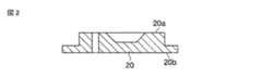
図1は、本発明の第1の実施の形態に係るレンズ付発光ダイオード装置10を示す縦断面図である。レンズ付発光ダイオード装置10は、リードフレーム20(電極が形成された支持部材)と、このリードフレーム20上に形成された外囲器30と、外囲器30内部に設けられ、後述する発光ダイオード22及びボンディングワイヤ23を封止する封止部40と、封止部40の上部に配置されたレンズ部50とを備えている。 FIG. 1 is a longitudinal sectional view showing a lens-equipped light-
リードフレーム20の表面20a側には、複数の電極21が形成され、この電極21には、発光ダイオード22が実装されている。発光ダイオード22の一方の電極にはボンディングワイヤ23が接続され、ボンディングワイヤ23は電極21に接続されている。なお、図1中20bはリードフレーム20の裏面を示している。 A plurality of
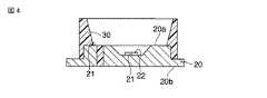
外囲器30を形成する第1の樹脂は、PPA、PC、エポキシ等の白色系の熱可塑性樹脂を用いる。また、封止部40を形成する第2の樹脂は、透明なエポキシ、シリコン等の熱硬化性樹脂やUV硬化性樹脂を用いる。白色光を発光する装置の場合には、波長変換用の蛍光体がこれらの樹脂に混合されることもある。さらに、レンズ部50を形成する第3の樹脂は透明なシリコン、エポキシ等の熱硬化性樹脂、あるいは、PMMA、PC、COP等の熱可塑性樹脂を用いる。 The first resin that forms the
次に、上述したレンズ付発光ダイオード装置10の製造工程について説明する。まず、図2に示すようにリードフレーム20を準備し、図3に示すように、リードフレームに発光ダイオード素子をダイマウント材(不図示)によって実装する。次に、これらを射出成形金型内にインサートし、図4に示すように、第1の白色の熱可塑性樹脂によって外囲器30を形成する。 Next, a manufacturing process of the above-described lens-equipped light-emitting
次に、図5に示すように、発光ダイオード素子22の電極とリードフレーム20の電極21とをワイヤボンディングした後に、発光ダイオード素子22の周囲に第2の封止樹脂を用いて封止部40を形成する。このとき、封止部40の形成は、金型を用いた射出成形でも、ポッティング法による成形でもよい。 Next, as shown in FIG. 5, after the electrode of the light
これらを再度、射出成形金型の内部にインサートし、図6に示すように透明の第3の樹脂を用いてレンズ部50を一体成形する。熱硬化性樹脂を用いる場合には、LIM成形法が採用され、熱可塑性樹脂の場合には射出成形法が採用される。 These are again inserted into the inside of the injection mold, and the
このように構成されたレンズ付発光ダイオード装置10では、レンズ部50の成形と外囲器30への取り付けを同時に行うことができるため、別工程で製造した樹脂レンズを外囲器に取り付ける工程及び光軸調整工程が不要となり、組み立て工程の低コスト化が可能となる。 In the light emitting diode device with a
一方、レンズ部50と外囲器30間に生じる間隙や、レンズ部50と封止部40間に生じる間隙を防止することができ、光取り出し効率を向上することができる。また、レンズ部50と封止部40の境界面において樹脂同士の融合が生じるため、取り付け強度を向上することが可能である。 On the other hand, a gap generated between the
上述したように、本発明の第1の実施の形態に係るレンズ付発光ダイオード装置によれば、光取出効率及び信頼性に優れるとともに、製造コストを低減することが可能となる。 As described above, the lens-equipped light-emitting diode device according to the first embodiment of the present invention is excellent in light extraction efficiency and reliability, and can reduce the manufacturing cost.
図7は、本発明の第2の実施の形態に係るレンズ付発光ダイオード装置10Aを示す縦断面図である。図7において、図1と同一機能部分には同一符号を付し、その詳細な説明は省略する。 FIG. 7 is a longitudinal sectional view showing a lens-equipped light
レンズ部50には、リードフレーム20を貫通し、発光ダイオード22が搭載されていない裏面20b側まで貫通する貫通部51が設けられ、この貫通部51の先端部52においてリードフレーム20に係止されている。 The
本実施の形態に係るレンズ付発光ダイオード装置10Aにおいても、上述したレンズ付発光ダイオード装置10と同様の効果を得ることができる。さらに、以下のような効果がある。すなわち、外囲器30とレンズ部50を構成する樹脂が異なる場合には、外囲器30とレンズ部50との密着強度の確保が困難である。このため、レンズ部50の一体成形時に透明樹脂をリードフレーム20の裏面20bにまで充填することで貫通部51を形成し、レンズ部50の脱落を防止する。これにより、密着強度を向上することができ、信頼性を向上させることができる。また、レンズ部51を形成する第3の樹脂として、収縮率や線膨張係数が大きい樹脂を用いることにより、効果を増大させることができる。なお、第3の樹脂を熱可塑性樹脂又は熱硬化性樹脂とした場合に用いることができる。 Also in the lens-equipped light-
図8は、本発明の第3の実施の形態に係るレンズ付発光ダイオード装置10Bを示す縦断面図である。図8において、図1と同一機能部分には同一符号を付し、その詳細な説明は省略する。 FIG. 8 is a longitudinal sectional view showing a lens-mounted light
レンズ部50には、外囲器30及びリードフレーム20を貫通し、発光ダイオード22が搭載されていない裏面20b側まで貫通する貫通部53が設けられ、この貫通部53の先端部54においてリードフレーム20に係止されている。 The
本実施の形態に係るレンズ付発光ダイオード装置10Bにおいても、上述したレンズ付発光ダイオード装置10Aと同様の効果を得ることができる。 Also in the light emitting diode device with
図9は、本発明の第4の実施の形態に係るレンズ付発光ダイオード装置10Cを示す縦断面図である。図9において、図1と同一機能部分には同一符号を付し、その詳細な説明は省略する。 FIG. 9 is a longitudinal sectional view showing a lens-equipped light emitting diode device 10C according to a fourth embodiment of the present invention. 9, the same functional parts as those in FIG. 1 are denoted by the same reference numerals, and detailed description thereof is omitted.
本実施の形態においては、外囲器30の上縁部に、微小なリブ31が設けられている。本実施の形態に係るレンズ付発光ダイオード装置10Cにおいても、上述したレンズ付発光ダイオード装置10と同様の効果を得ることができるとともに、レンズ部50を成形する際に、透明樹脂の熱によって微細なリブ31のみが再溶融し、レンズ部50と溶着する。この場合、融点が高い樹脂を用いることにより、溶着強度を高くすることができる。なお、この場合の第1の樹脂及び第3の樹脂は、熱可塑性樹脂となる。 In the present embodiment,
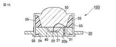
図10は、本発明の第5の実施の形態に係るレンズ付発光ダイオード装置10Dを示す縦断面図である。図10において、図1と同一機能部分には同一符号を付し、その詳細な説明は省略する。 FIG. 10 is a longitudinal sectional view showing a lens-equipped light-emitting diode device 10D according to the fifth embodiment of the present invention. 10, the same functional parts as those in FIG. 1 are denoted by the same reference numerals, and detailed description thereof is omitted.
リードフレーム20には、切欠部24が設けられている。また、レンズ部50には、リードフレーム20を貫通し、発光ダイオード22が搭載されていない裏面20bにまで延設された係止部55が設けられ、その先端部56が切欠部24に係合している。 The
本実施の形態に係るレンズ付発光ダイオード装置10Dにおいても、上述したレンズ付発光ダイオード装置10Aと同様の効果を得ることができる。 Also in the light emitting diode device with lens 10D according to the present embodiment, it is possible to obtain the same effect as the above-described light emitting diode device with
図11は、本発明の第6の実施の形態に係るレンズ付発光ダイオード装置10Eを示す縦断面図である。図11において、図1と同一機能部分には同一符号を付し、その詳細な説明は省略する。 FIG. 11 is a longitudinal sectional view showing a lens-equipped light emitting
レンズ付発光ダイオード装置10Eでは、上述したレンズ付発光ダイオード装置10Dとは異なる側面に係止部55を設けた場合に適用できるものである。リードフレーム20には、切欠部24が設けられている。また、レンズ部50には、リードフレーム20の側面に沿って延設され、発光ダイオード22が搭載されていない裏面20bにまで延設された係止部55が設けられ、その先端部56が切欠部24に係合している。 The lens-equipped light-emitting
本実施の形態に係るレンズ付発光ダイオード装置10Eにおいても、上述したレンズ付発光ダイオード装置10Dと同様の効果を得ることができる。レンズ付発光ダイオード装置10Eでは、係止部55をリードフレーム20を貫通させる必要が無い。 Also in the light emitting diode device with
図12は、本発明の第7の実施の形態に係るレンズ付発光ダイオード装置10Fを示す縦断面図である。図12において、図1と同一機能部分には同一符号を付し、その詳細な説明は省略する。 FIG. 12 is a longitudinal sectional view showing a lens-mounted light emitting
外囲器30には、貫通孔32が設けられている。また、レンズ部50には、貫通孔32を貫通する係止部57が設けられ、その先端部58が貫通孔32に係合している。なお、貫通孔32の代わりに切欠部を設けるようにしてもよい。 The
本実施の形態に係るレンズ付発光ダイオード装置10Fにおいても、上述したレンズ付発光ダイオード装置10Aと同様の効果を得ることができる。 In the lens-equipped light-emitting
なお、上述した各実施の形態における構造・工程はその一例であり、適宜置換可能なことは勿論である。例えば、発光ダイオード素子22の電極と外部電極21との接続は、ワイヤボンディングではなく、フリップチップボンディングでもよい。また、製造工程については、リードフレーム20に白色樹脂で外囲器30を形成し、その後に発光ダイオード素子22の実装を行ってもよい。さらに、リードフレーム20ではなく、電極が形成された支持部材、例えばガラスエポキシ基板、セラミック基板でも射出成形によるレンズ一体成形は可能である。 In addition, the structure and process in each embodiment mentioned above are the examples, and of course can be substituted suitably. For example, the connection between the electrode of the light emitting
なお、本発明は上記実施形態そのままに限定されるものではなく、実施段階ではその要旨を逸脱しない範囲で構成要素を変形して具体化できる。また、上記実施形態に開示されている複数の構成要素の適宜な組み合わせにより、種々の発明を形成できる。例えば、実施形態に示される全構成要素から幾つかの構成要素を削除してもよい。さらに、異なる実施形態にわたる構成要素を適宜組み合わせてもよい。 Note that the present invention is not limited to the above-described embodiment as it is, and can be embodied by modifying the constituent elements without departing from the scope of the invention in the implementation stage. In addition, various inventions can be formed by appropriately combining a plurality of components disclosed in the embodiment. For example, some components may be deleted from all the components shown in the embodiment. Furthermore, constituent elements over different embodiments may be appropriately combined.
10,10A〜10F…レンズ付発光ダイオード装置、20…リードフレーム(電極が形成された支持部材)、22…発光ダイオード、30…外囲器、40…封止部、50…レンズ部。 DESCRIPTION OF
Claims (4)
Translated fromJapaneseこの支持部材の上記電極に実装された発光ダイオードと、
上記支持部材上に設けられ、少なくとも上記発光ダイオードを含む領域を露出した状態
で中空部が形成された第1の樹脂からなる外囲器と、
上記外囲器の中空部の上記支持部材側に充填され、上記発光ダイオードを封止する第2の樹脂からなる封止部と、
上記封止部に積層して充填され、一体成形された第3の樹脂からなるレンズ部とを備え、
上記レンズ部は、上記外囲器及び上記支持部材の側面に沿って、上記支持部材の上記発光ダイオードが搭載された面とは反対側の面にまで延設し、この反対側の面に係合することを特徴とするレンズ付発光ダイオード装置。A support member on which an electrode is formed;
A light emitting diode mounted on the electrode of the support member;
An envelope made of a first resin provided on the support member and having a hollow portion formed in a state where at least a region including the light emitting diode is exposed;
A sealing portion made of a second resin that is filled on the support member side of the hollow portion of the envelope and seals the light emitting diode;
A lens portion made of a third resin that is laminated and filled in the sealing portion and is integrally molded;
The lens portion extends along a side surface of the envelope and the support member to a surface of the support member opposite to the surface on which the light emitting diode is mounted, and is engaged with the surface on the opposite side. A light-emitting diode device with a lens, wherein
ダイオード装置。2. The light emitting diode device with a lens according to claim 1, wherein the first resin is a white resin.
れらの透明樹脂に波長変換用の蛍光体を混合したことを特徴とする請求項1記載のレンズ
付発光ダイオード装置。2. The lens-attached lens according to claim 1, wherein the second resin is a transparent thermosetting resin or a UV curable resin, or a phosphor for wavelength conversion is mixed with these transparent resins. Light emitting diode device.
請求項1記載のレンズ付発光ダイオード装置。2. The lens-equipped light-emitting diode device according to claim 1, wherein the third resin is a transparent thermosetting resin or a thermoplastic resin.
Priority Applications (4)
| Application Number | Priority Date | Filing Date | Title |
|---|---|---|---|
| JP2005373498AJP4965858B2 (en) | 2005-12-26 | 2005-12-26 | LED device with lens |
| CN200610129054.3ACN1992361B (en) | 2005-12-26 | 2006-09-05 | Light-emitting diode device with lens |
| US11/613,503US7378647B2 (en) | 2005-12-26 | 2006-12-20 | Lens-equipped light-emitting diode device having an integrally molded lens unit being laminated on a sealing portion |
| EP06026839AEP1801893A3 (en) | 2005-12-26 | 2006-12-22 | Lens-equipped light-emitting diode device and method of manufacturing the same |
Applications Claiming Priority (1)
| Application Number | Priority Date | Filing Date | Title |
|---|---|---|---|
| JP2005373498AJP4965858B2 (en) | 2005-12-26 | 2005-12-26 | LED device with lens |
Publications (2)
| Publication Number | Publication Date |
|---|---|
| JP2007180069A JP2007180069A (en) | 2007-07-12 |
| JP4965858B2true JP4965858B2 (en) | 2012-07-04 |
Family
ID=37888282
Family Applications (1)
| Application Number | Title | Priority Date | Filing Date |
|---|---|---|---|
| JP2005373498AExpired - Fee RelatedJP4965858B2 (en) | 2005-12-26 | 2005-12-26 | LED device with lens |
Country Status (4)
| Country | Link |
|---|---|
| US (1) | US7378647B2 (en) |
| EP (1) | EP1801893A3 (en) |
| JP (1) | JP4965858B2 (en) |
| CN (1) | CN1992361B (en) |
Families Citing this family (28)
| Publication number | Priority date | Publication date | Assignee | Title |
|---|---|---|---|---|
| US6697658B2 (en) | 2001-07-02 | 2004-02-24 | Masimo Corporation | Low power pulse oximeter |
| US7647083B2 (en) | 2005-03-01 | 2010-01-12 | Masimo Laboratories, Inc. | Multiple wavelength sensor equalization |
| US8044412B2 (en) | 2006-01-20 | 2011-10-25 | Taiwan Semiconductor Manufacturing Company, Ltd | Package for a light emitting element |
| JP2009094282A (en)* | 2007-10-09 | 2009-04-30 | Cosmo Electronics Corp | High-power light emitting diode structure |
| KR101488448B1 (en) | 2007-12-06 | 2015-02-02 | 서울반도체 주식회사 | LED package and manufacturing method thereof |
| JP2009206370A (en)* | 2008-02-28 | 2009-09-10 | Apic Yamada Corp | Substrate for led package, method for manufacturing substrate for led package, molding metal mold for substrate for led package, led package and method for manufacturing led package |
| US20100004518A1 (en) | 2008-07-03 | 2010-01-07 | Masimo Laboratories, Inc. | Heat sink for noninvasive medical sensor |
| US8515509B2 (en) | 2008-08-04 | 2013-08-20 | Cercacor Laboratories, Inc. | Multi-stream emitter for noninvasive measurement of blood constituents |
| GB2466633A (en)* | 2008-12-12 | 2010-07-07 | Glory Science Co Ltd | Method of manufacturing a light emitting unit |
| JP5368809B2 (en)* | 2009-01-19 | 2013-12-18 | ローム株式会社 | LED module manufacturing method and LED module |
| CN101852384B (en)* | 2009-03-31 | 2013-08-28 | 光宝科技股份有限公司 | Method of forming a lens structure for a light emitting diode and related architecture |
| TWI485878B (en)* | 2009-04-01 | 2015-05-21 | Lite On Technology Corp | Method for forming a lens structure of a light-emitting diode and related structure |
| TW201041192A (en)* | 2009-05-11 | 2010-11-16 | Semi Photonics Co Ltd | LED device with a roughened light extraction structure and manufacturing methods thereof |
| KR101114197B1 (en)* | 2010-08-09 | 2012-02-22 | 엘지이노텍 주식회사 | Light emitting device and lighting system having same |
| US9085728B2 (en)* | 2011-01-28 | 2015-07-21 | Showa Denko K.K. | Composition containing quantum dot fluorescent body, molded body of quantum dot fluorescent body dispersion resin, structure containing quantum dot fluorescent body, light-emitting device, electronic apparatus, mechanical device, and method for producing molded body of quantum dot fluorescent body dispersion resin |
| KR20140048319A (en) | 2011-08-05 | 2014-04-23 | 지유아이 글로벌 프로덕츠 엘티디. | Apparatus for cleaning view screens and lenses and method for the use thereof |
| TW201415673A (en)* | 2012-10-03 | 2014-04-16 | Lextar Electronics Corp | Illuminating device |
| US20200137906A9 (en) | 2012-11-05 | 2020-04-30 | Gui Global Products, Ltd. | Devices and accessories employing a living hinge |
| KR101433261B1 (en) | 2013-01-15 | 2014-08-27 | 루미마이크로 주식회사 | Light Emitting Device |
| CN103400927B (en)* | 2013-07-25 | 2016-04-27 | 广东晶科电子股份有限公司 | A kind of high reliability LED support and LED component thereof |
| JP2015050016A (en)* | 2013-08-30 | 2015-03-16 | 東芝ライテック株式会社 | Light emitting module and lighting device |
| KR102076243B1 (en)* | 2013-09-04 | 2020-02-12 | 엘지이노텍 주식회사 | A light emitting device package |
| JP6179555B2 (en)* | 2015-06-01 | 2017-08-16 | 日亜化学工業株式会社 | Light emitting device |
| JP6110528B2 (en)* | 2016-02-03 | 2017-04-05 | 京セラコネクタプロダクツ株式会社 | Semiconductor light emitting device holder and semiconductor light emitting device module |
| JP6680302B2 (en)* | 2018-01-10 | 2020-04-15 | 日亜化学工業株式会社 | Light emitting device |
| WO2021146333A1 (en) | 2020-01-13 | 2021-07-22 | Masimo Corporation | Wearable device with physiological parameters monitoring |
| JP7299537B2 (en)* | 2020-03-18 | 2023-06-28 | 日亜化学工業株式会社 | light emitting device |
| EP4370022A1 (en) | 2021-07-13 | 2024-05-22 | Masimo Corporation | Wearable device with physiological parameters monitoring |
Family Cites Families (25)
| Publication number | Priority date | Publication date | Assignee | Title |
|---|---|---|---|---|
| JPS63318173A (en)* | 1987-06-19 | 1988-12-27 | New Japan Radio Co Ltd | Manufacture of optical semiconductor device |
| JPH03254162A (en)* | 1990-03-02 | 1991-11-13 | Mitsui Petrochem Ind Ltd | Cap for light emission element, light emission element employing the cap and manufacturing method and device therefor |
| IT1265106B1 (en)* | 1993-07-23 | 1996-10-30 | Solari Udine Spa | OPTICAL SYSTEM FOR LIGHT-EMITTING DIODES |
| JPH07307492A (en)* | 1994-05-11 | 1995-11-21 | Mitsubishi Cable Ind Ltd | Led aggregate module and its manufacture |
| JP3141373B2 (en)* | 1996-01-18 | 2001-03-05 | 日亜化学工業株式会社 | Photoelectric device |
| JP3492178B2 (en)* | 1997-01-15 | 2004-02-03 | 株式会社東芝 | Semiconductor light emitting device and method of manufacturing the same |
| US6274890B1 (en)* | 1997-01-15 | 2001-08-14 | Kabushiki Kaisha Toshiba | Semiconductor light emitting device and its manufacturing method |
| JP2000108144A (en)* | 1998-10-06 | 2000-04-18 | Taiyo Ltd | Manufacture of parts |
| JP2000156528A (en)* | 1998-11-19 | 2000-06-06 | Sharp Corp | Light emitting element |
| JP3913435B2 (en)* | 2000-02-29 | 2007-05-09 | 株式会社小糸製作所 | Manufacturing method of vehicular lamp |
| JP3614776B2 (en)* | 2000-12-19 | 2005-01-26 | シャープ株式会社 | Chip component type LED and its manufacturing method |
| JP2002299699A (en)* | 2001-03-30 | 2002-10-11 | Sumitomo Electric Ind Ltd | Light emitting device and method of manufacturing the same |
| JP2004071908A (en)* | 2002-08-07 | 2004-03-04 | Matsushita Electric Works Ltd | Light emitting device |
| US6682331B1 (en)* | 2002-09-20 | 2004-01-27 | Agilent Technologies, Inc. | Molding apparatus for molding light emitting diode lamps |
| JP2004265979A (en)* | 2003-02-28 | 2004-09-24 | Noritsu Koki Co Ltd | Light emitting diode light source unit |
| JP4599857B2 (en) | 2003-04-24 | 2010-12-15 | 日亜化学工業株式会社 | Semiconductor device and manufacturing method thereof |
| JP2005197369A (en)* | 2004-01-05 | 2005-07-21 | Toshiba Corp | Optical semiconductor device |
| JP2005223216A (en)* | 2004-02-06 | 2005-08-18 | Matsushita Electric Ind Co Ltd | Luminescent light source, lighting device and display device |
| KR100585916B1 (en)* | 2004-03-30 | 2006-06-01 | 서울반도체 주식회사 | Light emitting diode |
| US7280288B2 (en)* | 2004-06-04 | 2007-10-09 | Cree, Inc. | Composite optical lens with an integrated reflector |
| JP4146406B2 (en)* | 2004-08-31 | 2008-09-10 | シャープ株式会社 | Light emitting device and method for manufacturing light emitting device |
| US7855395B2 (en)* | 2004-09-10 | 2010-12-21 | Seoul Semiconductor Co., Ltd. | Light emitting diode package having multiple molding resins on a light emitting diode die |
| JP2006261049A (en)* | 2005-03-18 | 2006-09-28 | Koizumi Sangyo Corp | Multi-point light source unit |
| JP2006351816A (en)* | 2005-06-16 | 2006-12-28 | Toshiaki Inoue | Shell type light emitting diode lens cap |
| JP2007080879A (en)* | 2005-09-09 | 2007-03-29 | Matsushita Electric Works Ltd | Led unit |
- 2005
- 2005-12-26JPJP2005373498Apatent/JP4965858B2/ennot_activeExpired - Fee Related
- 2006
- 2006-09-05CNCN200610129054.3Apatent/CN1992361B/ennot_activeExpired - Fee Related
- 2006-12-20USUS11/613,503patent/US7378647B2/ennot_activeExpired - Fee Related
- 2006-12-22EPEP06026839Apatent/EP1801893A3/ennot_activeWithdrawn
Also Published As
| Publication number | Publication date |
|---|---|
| EP1801893A3 (en) | 2011-08-03 |
| US7378647B2 (en) | 2008-05-27 |
| CN1992361A (en) | 2007-07-04 |
| US20070145255A1 (en) | 2007-06-28 |
| EP1801893A2 (en) | 2007-06-27 |
| CN1992361B (en) | 2010-05-12 |
| JP2007180069A (en) | 2007-07-12 |
Similar Documents
| Publication | Publication Date | Title |
|---|---|---|
| JP4965858B2 (en) | LED device with lens | |
| JP4945106B2 (en) | Semiconductor light emitting device | |
| CN100590779C (en) | Surface mount multi-channel optical coupler | |
| JP5596901B2 (en) | Power light emitting die package having a reflective lens and method of manufacturing the same | |
| JP5819414B2 (en) | Surface mountable optoelectronic component and method for manufacturing surface mountable optoelectronic component | |
| JP2005197369A (en) | Optical semiconductor device | |
| JP2010516050A (en) | Housing for optoelectronic components and placement of optoelectronic components in the housing | |
| JP2002185046A (en) | Chip component type LED and method of manufacturing the same | |
| KR20100115365A (en) | Light emitting device | |
| JP2009200321A (en) | Light-emitting device and its manufacturing method | |
| CN101657748A (en) | Optical coupler package | |
| US9209338B2 (en) | Optical device with through-hole cavity | |
| US7919788B2 (en) | Assembly of a heat dissipating base and a lead frame for a light emitting diode packaging device and method for making the same | |
| JP4884074B2 (en) | Semiconductor light emitting device | |
| KR20100097039A (en) | Light-emitting device | |
| KR101945057B1 (en) | Base for optical semiconductor device and method for preparing the same, and optical semiconductor device | |
| KR101202169B1 (en) | Method of fabricating light emitting diode package having multi-molding members | |
| JP2020092251A (en) | Light-emitting device and manufacturing method thereof | |
| JP2008172140A (en) | Light emitting device with cushioning material between housing and upper hard protection material | |
| JP2006269783A (en) | Optical semiconductor package | |
| US9184149B2 (en) | Semiconductor device with an interlocking wire bond | |
| JP2011171693A (en) | Light emitting device and method of manufacturing the same | |
| JP2008251759A (en) | Lead frame structure with resin cup and manufacturing method thereof | |
| JPS59149072A (en) | light emitting semiconductor device | |
| KR101025994B1 (en) | Light emitting diode package |
Legal Events
| Date | Code | Title | Description |
|---|---|---|---|
| A621 | Written request for application examination | Free format text:JAPANESE INTERMEDIATE CODE: A621 Effective date:20081225 | |
| A977 | Report on retrieval | Free format text:JAPANESE INTERMEDIATE CODE: A971007 Effective date:20110427 | |
| A131 | Notification of reasons for refusal | Free format text:JAPANESE INTERMEDIATE CODE: A131 Effective date:20111220 | |
| A521 | Request for written amendment filed | Free format text:JAPANESE INTERMEDIATE CODE: A523 Effective date:20120220 | |
| TRDD | Decision of grant or rejection written | ||
| A01 | Written decision to grant a patent or to grant a registration (utility model) | Free format text:JAPANESE INTERMEDIATE CODE: A01 Effective date:20120306 | |
| A01 | Written decision to grant a patent or to grant a registration (utility model) | Free format text:JAPANESE INTERMEDIATE CODE: A01 | |
| A61 | First payment of annual fees (during grant procedure) | Free format text:JAPANESE INTERMEDIATE CODE: A61 Effective date:20120330 | |
| FPAY | Renewal fee payment (event date is renewal date of database) | Free format text:PAYMENT UNTIL: 20150406 Year of fee payment:3 | |
| LAPS | Cancellation because of no payment of annual fees |