JP4964223B2 - Gas distribution apparatus and substrate processing chamber - Google Patents
Gas distribution apparatus and substrate processing chamberDownload PDFInfo
- Publication number
- JP4964223B2 JP4964223B2JP2008500824AJP2008500824AJP4964223B2JP 4964223 B2JP4964223 B2JP 4964223B2JP 2008500824 AJP2008500824 AJP 2008500824AJP 2008500824 AJP2008500824 AJP 2008500824AJP 4964223 B2JP4964223 B2JP 4964223B2
- Authority
- JP
- Japan
- Prior art keywords
- gas
- distribution device
- gas distribution
- inclined step
- central
- Prior art date
- Legal status (The legal status is an assumption and is not a legal conclusion. Google has not performed a legal analysis and makes no representation as to the accuracy of the status listed.)
- Active
Links
Images


Classifications
- H—ELECTRICITY
- H01—ELECTRIC ELEMENTS
- H01J—ELECTRIC DISCHARGE TUBES OR DISCHARGE LAMPS
- H01J37/00—Discharge tubes with provision for introducing objects or material to be exposed to the discharge, e.g. for the purpose of examination or processing thereof
- H01J37/32—Gas-filled discharge tubes
- H01J37/32431—Constructional details of the reactor
- H01J37/3244—Gas supply means
- H01J37/32449—Gas control, e.g. control of the gas flow
- H—ELECTRICITY
- H01—ELECTRIC ELEMENTS
- H01L—SEMICONDUCTOR DEVICES NOT COVERED BY CLASS H10
- H01L21/00—Processes or apparatus adapted for the manufacture or treatment of semiconductor or solid state devices or of parts thereof
- H01L21/02—Manufacture or treatment of semiconductor devices or of parts thereof
- H—ELECTRICITY
- H01—ELECTRIC ELEMENTS
- H01J—ELECTRIC DISCHARGE TUBES OR DISCHARGE LAMPS
- H01J37/00—Discharge tubes with provision for introducing objects or material to be exposed to the discharge, e.g. for the purpose of examination or processing thereof
- H01J37/32—Gas-filled discharge tubes
- H—ELECTRICITY
- H01—ELECTRIC ELEMENTS
- H01J—ELECTRIC DISCHARGE TUBES OR DISCHARGE LAMPS
- H01J37/00—Discharge tubes with provision for introducing objects or material to be exposed to the discharge, e.g. for the purpose of examination or processing thereof
- H01J37/32—Gas-filled discharge tubes
- H01J37/32009—Arrangements for generation of plasma specially adapted for examination or treatment of objects, e.g. plasma sources
- H01J37/32082—Radio frequency generated discharge
- H—ELECTRICITY
- H01—ELECTRIC ELEMENTS
- H01J—ELECTRIC DISCHARGE TUBES OR DISCHARGE LAMPS
- H01J37/00—Discharge tubes with provision for introducing objects or material to be exposed to the discharge, e.g. for the purpose of examination or processing thereof
- H01J37/32—Gas-filled discharge tubes
- H01J37/32431—Constructional details of the reactor
- H01J37/3244—Gas supply means
- H—ELECTRICITY
- H01—ELECTRIC ELEMENTS
- H01L—SEMICONDUCTOR DEVICES NOT COVERED BY CLASS H10
- H01L21/00—Processes or apparatus adapted for the manufacture or treatment of semiconductor or solid state devices or of parts thereof
- H—ELECTRICITY
- H01—ELECTRIC ELEMENTS
- H01J—ELECTRIC DISCHARGE TUBES OR DISCHARGE LAMPS
- H01J2237/00—Discharge tubes exposing object to beam, e.g. for analysis treatment, etching, imaging
- H01J2237/32—Processing objects by plasma generation
- H01J2237/33—Processing objects by plasma generation characterised by the type of processing
- H01J2237/332—Coating
- H01J2237/3321—CVD [Chemical Vapor Deposition]
Landscapes
- Engineering & Computer Science (AREA)
- Physics & Mathematics (AREA)
- Plasma & Fusion (AREA)
- Chemical & Material Sciences (AREA)
- Analytical Chemistry (AREA)
- Condensed Matter Physics & Semiconductors (AREA)
- General Physics & Mathematics (AREA)
- Manufacturing & Machinery (AREA)
- Computer Hardware Design (AREA)
- Microelectronics & Electronic Packaging (AREA)
- Power Engineering (AREA)
- Chemical Vapour Deposition (AREA)
Description
Translated fromJapanese[0001]本発明は、一般に、半導体の製造および、より具体的には、半導体処理チャンバ内の分配装置および最上部ガスバッフルに関する。 [0001] The present invention relates generally to semiconductor manufacturing and, more particularly, to a dispensing device and top gas baffle in a semiconductor processing chamber.
[0002]基板上に所望の材料の膜または薄い層を形成するために、化学気相堆積(CVD)は、半導体産業で使用されているガス反応処理である。一部の高密度プラズマ(HDP)増強型CVD処理は、RF発生プラズマを使用して物理的イオンを発生させると共に反応性化学ガスを使用し、負にバイアスされた基板表面上に正に荷電されたプラズマイオンを上記表面に対して垂直に近い角度で吸引することにより、或いは、上記表面に対して好ましい角度における基板表面の指向性バイアスにより、膜の堆積を増強する。集積回路(IC)の製作における一つの目標は、非常に薄く、均一な膜を基板上に、高スループットで形成することである。多くの要素(電源及び幾何学的形状の型と幾何学的形状、ガス分配システムと関連排気、基板の加熱と冷却、チャンバ構成、設計、対称性、チャンバ表面の組成と温度制御、チャンバ内に蓄積される材料など)は、処理システムと、そのシステムにより実行される処理を評価するときに考慮されなければならない。 [0002] Chemical vapor deposition (CVD) is a gas reaction process used in the semiconductor industry to form a film or thin layer of a desired material on a substrate. Some high density plasma (HDP) enhanced CVD processes use RF generated plasma to generate physical ions and reactive chemical gases that are positively charged on the negatively biased substrate surface. The deposition of the film is enhanced by attracting the plasma ions at an angle close to perpendicular to the surface or by a directional bias on the substrate surface at a preferred angle to the surface. One goal in integrated circuit (IC) fabrication is to form very thin, uniform films on a substrate with high throughput. Many elements (power and geometry type and geometry, gas distribution system and associated exhaust, substrate heating and cooling, chamber configuration, design, symmetry, chamber surface composition and temperature control, within chamber Material, etc.) must be considered when evaluating the processing system and the processing performed by the system.
[0003]むらがあるガス分配は、半導体製作で直面する一つの問題であり、堆積の均一性に影響する。既知の一チャンバ構成において、ガスプレナムは処理領域の周辺に備えられ、複数のノズルが放射状内側に伸びており、ガスを基板表面に提供する。そのような設計における難題は、基板表面にわたりガスを均等に分配することであり、そのためにも、基板の中央に向かうというより基板の縁に向かって多くのガスが供給されないことである。最上部のガスノズルは、基板支持部材の直接上方に位置決めされているが、堆積均一性を改善する為に使用可能である。 [0003] Uneven gas distribution is one problem faced in semiconductor fabrication and affects deposition uniformity. In one known chamber configuration, a gas plenum is provided around the processing region, and a plurality of nozzles extend radially inward to provide gas to the substrate surface. The challenge in such a design is to distribute the gas evenly across the substrate surface, and for that reason too much gas is not supplied towards the edge of the substrate rather than towards the center of the substrate. The top gas nozzle is positioned directly above the substrate support member, but can be used to improve deposition uniformity.
[0004]最上部のガスノズルを使用することにより得られる改善にも拘わらず、更なる改善及び/又は代替技術が、基板の表面でのガス分配の均一性を高める為に望ましい。 [0004] Despite the improvements obtained by using the top gas nozzle, further improvements and / or alternative techniques are desirable to increase the uniformity of gas distribution at the surface of the substrate.
[0005]本発明は、半導体を処理する為の装置及びチャンバ内にガスを導入する方法を含む技術を提供する。より詳しくは、本発明の実施形態は、半導体処理チャンバ内の基板上の処理ガスの均一性を高めることを目的とする。 [0005] The present invention provides a technique including an apparatus for processing a semiconductor and a method for introducing a gas into a chamber. More particularly, embodiments of the present invention aim to increase the uniformity of process gas on a substrate in a semiconductor processing chamber.
[0006]本発明の一実施形態において、ガス分配装置は、本体を有し、その本体は、本体から離れてガスを外側に導くように適合された上部表面と、その上部表面の反対側にある下部表面と、を有する。下部表面は、中央部と、段部表面により中央部から分離された凹んだ周辺部と、を有する。本体は、更に、ガス入口と、段部表面に配置された複数のガス出口と、複数のガス出口に入口を連結するガス通路と、を含む。 [0006] In one embodiment of the present invention, a gas distribution device has a body, the body being on an upper surface adapted to guide the gas away from the body and on the opposite side of the upper surface. A lower surface. The lower surface has a central portion and a recessed peripheral portion separated from the central portion by a step surface. The main body further includes a gas inlet, a plurality of gas outlets arranged on the step surface, and a gas passage connecting the inlet to the plurality of gas outlets.
[0007]さらに、本発明の他の実施形態において、基板処理チャンバは、天井および側壁を有する包囲体と、基板を支持できる基板支持体と、を含む。ガス分配装置は、基板支持体の上方中央に位置決めされている。ガス分配装置は、バッフルを含む本体を備え、バッフルは、本体から離れてガスを外側に包囲体の側壁に向けて導くように適合された上部表面と、上部表面の反対側にあり基板支持体から離間された下部表面と、を有する。下部表面は、中央部と、段部表面により中央部から分離され凹んだ周辺部と、を有する。本体は、更に、ガス入口と、段部表面に配置された複数のガス出口と、複数のガス出口に入口を連結するガス通路と、を含む。 [0007] Further, in another embodiment of the present invention, the substrate processing chamber includes an enclosure having a ceiling and sidewalls, and a substrate support capable of supporting the substrate. The gas distributor is positioned in the upper center of the substrate support. The gas distribution device includes a body including a baffle, the baffle being on a substrate support opposite to the upper surface and an upper surface adapted to direct gas away from the body toward the side walls of the enclosure And a lower surface spaced from the lower surface. The lower surface has a central portion and a peripheral portion that is separated from the central portion by the stepped surface and is recessed. The main body further includes a gas inlet, a plurality of gas outlets arranged on the step surface, and a gas passage connecting the inlet to the plurality of gas outlets.
[0016]本発明は、ガスをチャンバ内に導入する方法と、半導体を処理する為の装置を含む技術を提供する。より詳しくは、本発明の実施形態は、半導体処理チャンバ内の基板上で処理ガスの均一性を高めることを目的とする。 [0016] The present invention provides a technique including a method for introducing a gas into a chamber and an apparatus for processing a semiconductor. More particularly, embodiments of the present invention are directed to increasing process gas uniformity on a substrate in a semiconductor processing chamber.
[0017]図1は、半導体処理の為の、以前に既知のガス分配装置の横断面図である。図1は、ガス偏向表面102およびガス分配装置面104を有するガス分配装置100を示す。ガス偏向表面102は、チャンバ洗浄処理中の洗浄ガス用通路を与える。洗浄ガスは、ガス分配装置の直下に置かれた基板支持部材(図示せず)ではなく、外形面102によりチャンバ壁に向けられている。ガス分配装置100は、基部106でチャンバ壁に連結されている。堆積ガスは、基端108でガス分配装置100に供給可能である。一組のアパーチャ110は、CVD処理中に堆積ガスを送る為にガス分配装置面104で配置されている。 [0017] FIG. 1 is a cross-sectional view of a previously known gas distribution apparatus for semiconductor processing. FIG. 1 shows a
[0018]図2は、本発明の一実施形態に従うガス分配装置の横断面図である。この図は、単に一実施例であるので、本願の請求項の範囲を不当に限定するものではない。当業者は、他の変形例、変更例、代替例を認識するであろう。示されるように、本発明は、ガスを半導体処理チャンバ内に導入する為のガス分配装置を提供する。ガス分配装置200は、あらゆる適した材料で形成可能であり、例えば、酸化アルミニウム(Al2O3)、窒化アルミニウム(AlN)、シリコンカーバイド(SiC)、ジルコニウム、石英、サファイヤ等が本実施例において可能であり、ガス分配装置200は単体である。[0018] FIG. 2 is a cross-sectional view of a gas distribution apparatus according to an embodiment of the present invention. This diagram is merely an example and should not unduly limit the scope of the claims herein. Those skilled in the art will recognize other variations, modifications, and alternatives. As shown, the present invention provides a gas distribution apparatus for introducing gas into a semiconductor processing chamber. The
[0019]ガス分配装置200は、ガス偏向表面202と、ガス分配装置面204と、を有する。ガス偏向表面202は、チャンバ洗浄処理中に洗浄ガスの為の通路を与える。洗浄ガスは、ガス分配装置の直下に置かれた基板支持部材(図示せず)でなく、チャンバ壁に向けられる。ガス分配装置200は、基部206でチャンバ壁に連結されている。CVD処理中、堆積ガスは、基端208でガス分配装置200に供給される。この堆積ガスは、アパーチャ210を出て、基板支持部材上の基板位置へと、ガス分配装置200を通って流れる。 [0019] The
[0020]図2に図示されるように、アパーチャ210は、段部212(隆起表面)で、ガス分配装置面204上に配置されている。段部212は、所定の径を有するガス分配装置面204で、楕円レベル、より好ましくは、円形レベルを形成可能である。直径は、約0.01インチから約3.00インチまでの範囲が可能である。段部212は、約0.60インチから約0.75インチまでの範囲で垂直の高さを有し、約90度から約15度までの範囲で傾斜を有することが可能である。段部212は、ガス分配装置200のガス分配を改善する。特に、堆積ガスは、段部212の結果、基板支持部材の周辺の更なる外側まで分散可能である。段部212の傾斜を減少させると、ガスは外側に更に分散する。 [0020] As illustrated in FIG. 2, the
[0021]特定の実施形態において、ガス分配装置200は、4つ、6つ、8つ、又は、それ以上のアパーチャ210を有することが可能である。これらのアパーチャ210は、段部212の周辺に沿って均等に分布され、或いは、その特定部分に対し重要性が付加されている。アパーチャ210の位置および数は、基板上の堆積ガスの均一な分配を達成するように、特定用途の為に調整可能である。同様に、アパーチャ210の径も調整可能である。径は、約0.005インチから約0.250インチの範囲が可能である。特定の実施形態において、アパーチャ210の径は、0.060インチになっている。 [0021] In certain embodiments, the
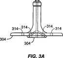
[0022]図3A(側面図)と図3B(平面図)は、洗浄ガス通路314を備えた本発明の一実施形態に従うガス分配装置を図示する。洗浄ガス通路314は、チャンバ洗浄処理中に洗浄ガスの一部をガス分配装置300を通ってガス分配装置面304まで通過させる。このように、ガス分配装置304は、容易に洗浄可能である。この特定の実施形態には、8つのガス通路314がある。しかし、他の実施形態において、洗浄ガス通路の数は、約50通路まで可能である。各々の処理ガス流路314の径は、約0.06から約0.25インチまでにあり、ガス分配装置面204の効果的な洗浄を見越している。 [0022] FIGS. 3A (side view) and 3B (plan view) illustrate a gas distribution apparatus according to one embodiment of the present invention with a
[0023]図4Aは、本発明の他の実施形態に従うガス分配装置400の横断面図である。単体のガス分配装置400は、ガス偏向表面402とガス分配装置面404を有する。ガス分配装置400は、基部406でチャンバ壁に連結されている。CVD処理中、堆積ガスは、基端408でガス分配装置400に供給されている。この堆積ガスは、ガス分配装置400を通り、アパーチャ410とフィード孔416を出て、基板支持部材(図示せず)上の基板位置に流れる。図4Bに図示されているように、アパーチャ410は、段部412でガス分配装置404に配置され、フィード孔416は、ガス分配装置400の側端部に配置されている。フィード孔416は、基板の縁に増加堆積をまかない、均一な分配の為にアパーチャ410を補充する。フィード孔416とアパーチャ410の数、位置、周辺は、特定用途の為に調整可能である。一つの特定実施形態において、ガス分配装置400は、8つのフィード孔416と4つのアパーチャ410を含む。他の実施形態において、ガス分配装置400は、アパーチャ410を有することなく、フィード孔416を有することが可能である。あるいは、ガス分配装置400は、フィード孔416を有することなく、アパーチャ410を含むことも可能である。 [0023] FIG. 4A is a cross-sectional view of a
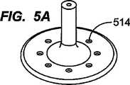
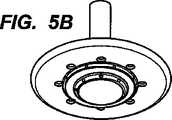
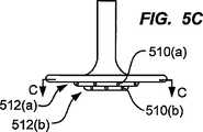
[0024]図5A−図5Gは、本発明の更に他の実施形態に従うガス分配装置500の様々な図を示す。ガス分配装置500は、洗浄ガス通路514と、2つの段部(段部512(a)、段部512(b))を含む。段部512(a)と段部512(b)は、ガス分配装置面504で、各々が、一組のアパーチャを統合している。段部の数を増やすことにより、ガス分配の更なる調整を可能にし、均一性を改善する。段部512(a)に含まれたアパーチャの数と位置は、段部512(b)と異なってもよい。たとえば、アパーチャ510(a)、510(b)は、中心点518から放射方向に整列されていない。 [0024] FIGS. 5A-5G show various views of a
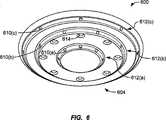
[0025]図6は、本発明の実施形態に従う三段型ガス分配装置600を図示する。ガス分配装置面604は、段部612(a)−(c)を含み、各々は、それぞれ、一組のアパーチャ610(a)−(c)を備える。三つの段部は、ガス分配の高度な改良の為に3つの制御領域を提供する。さらに、各アパーチャの長さが短いため、アパーチャ612の径は、高度な分配制御の為に減じられている。一つの特定実施形態において、ガス分配装置600は、2つの単体プレナムである。本発明の他の実施形態は、4つ、5つ、6つ、又はそれ以上の段部を含んでもよいことに留意されたい。 [0025] FIG. 6 illustrates a three-stage
[0026]図7A及び図7Bは、本発明の実施形態に従うガス分配装置段部の横断面図である。図7Aにおいて、ガス分配装置の段部は、ガス分配装置面で、トレッド部とライザ部とを含む。ライザ部は、トレッド部に対して直角、又は、好ましくは角度710でもよい。角度710は、約90度から約180度の範囲が可能である。特定の実施形態において、角度710は、約45度である。ガス分配装置面上のアパーチャは、段部のライザ部に配置されている。アパーチャは、ライザ部に対し直角であるか、或いは、図7Bに描写されているように、角度720である。(ライザ部に対し直角に孔を有することにより、小さな振動で、より正確な孔の機械加工を行う)例えば、角度720は、約15度から約120度までの範囲が可能である。
[0026] FIGS. 7A and 7B are cross-sectional views of gas distributor steps according to embodiments of the present invention. In FIG. 7A, the step portion of the gas distribution device includes atread portion and a riser portion on the gas distribution device surface. The riser portion may be perpendicular to thetread portion, or preferably at an
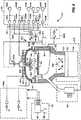
[0027]図8は、本発明の実施形態に従うガス分配装置811を有する典型的な処理チャンバシステムを図示する。図8は、一実施形態において、典型的なHDP−CVDシステム810の構造を概略的に図示する。システム810は、チャンバ813、真空システム870、ソースプラズマシステム880A、バイアス型プラズマシステム880B、ガス送出システム833,リモートプラズマ洗浄システム850を含む。 [0027] FIG. 8 illustrates an exemplary processing chamber system having a gas distributor 811 according to an embodiment of the present invention. FIG. 8 schematically illustrates the structure of a typical HDP-
[0028]チャンバ813の上部は、ドーム814を含み、ドーム814は、セラミック誘電材(酸化アルミニウム、窒化アルミニウム、サファイヤ、SiC、石英など)で形成されている。ヒータプレート823と冷却プレート824は、上にあり、両方とも熱的にドーム814に結合されている。ヒータプレート823と冷却プレート824は、約100℃から200℃の範囲にわたり±10℃以内でドーム温度を制御する。ドーム814は、プラズマ領域816の上限を規定する。プラズマ処理領域816は、基板817と基板支持部材818の上部表面により底で制限されている。 [0028] The upper portion of the
[0029]チャンバ813の下部は、本体部材822を含み、本体部材822は、真空システムにチャンバを接合する。基板支持部材818のベース部材821は、本体部材822上に取り付けられ、本体部材822と共に連続した内部表面を形成する。基板は、ロボットブレード(図示せず)により、チャンバ813の側部の挿入/除去用開口(図示せず)を通して、チャンバ813の内外に移送される。リフトピン(図示せず)は、モータ(図示せず)の制御下で、上昇され、その後、下降され、基板を上部ローディング位置857におけるロボットブレードから、基板が基板支持部材818の基板受領部819上に置かれる下部処理位置856まで移動する。基板受容部819は、静電チャック820を含み、静電チャック819は、基板処理中、基板支持部材818に基板を固定する。好ましい実施形態において、基板支持部材818は、酸化アルミニウムまたはアルミニウム・セラミック材料から形成されている。 [0029] The lower portion of
[0030]真空システム870は、スロットル本体825を含み、スロットル本体825は、ツインブレードスロットルバルブ826を収容し、ゲートバルブ827とターボ分子ポンプ828に付けられている。スロットル本体825は、ガス流に最小限の障害を提供するが、対称ポンピングを許容する点に留意されたい。ゲートバルブ827は、スロットル本体825からポンプ828を分離することができ、また、スロットルバルブ826が全開のとき、排気流量容積を制限することにより、チャンバ圧力を制御することができる。スロットルバルブ、ゲートバルブ、ターボ分子ポンプの配列により、約1ミリトールから約2トールの間でチャンバ圧力を正確かつ安定に制御することができる。 [0030] The
[0031]ガス送出システム833は、数個のソース834A−834Eからガスをチャンバに供給し、(数個だけが図示された)ガス送出ライン838を介して基板を処理する。当業者により理解されるように、ソース834A−834Eに対して使用される実際のソースと、チャンバ813に対する送出ライン838の実際の接続は、チャンバ813内で排出される洗浄処理と堆積に依存して変化する。ガスは、ガスリング837及び/又はガス分配装置811を通って導入される。 [0031] The
[0032]一実施形態において、第1ガスソース834A、第2ガスソース834B、第1ガス流コントローラ835A’、第2ガス流コントローラ835B’は、ガスリング837内のリングプレナムにガスを、ガス送出ライン838を介して供給する。ガスリング837は、ガスの一様な流れを基板上に供給する複数のソースガスノズル839(数個だけが図示)を有する。ノズル長とノズル角は、個々のチャンバ内部で特定処理の為に、ガス利用効率と均一プロファイルの調整を許容するように偏向されてもよい。好ましい実施形態において、ガスリング837は、12個のソースガスノズルを有し、これらは、アルミナ・セラミックから形成されている。 [0032] In one embodiment, the
[0033]ガスリング837も同様に、複数の酸化剤ガスノズル840(1個だけが図示)を有し、好ましい実施形態において、これらは、同一平面上にあり、ソースガスノズル839より短く、一実施形態では、本体プレナムからガスを受ける。幾つかの実施形態において、ガスをチャンバ813に噴射する前に、酸化剤ガスとソースガスを混合しないことが望ましい。他の実施形態では、酸化剤ガスとソースガスは、本体プレナムとガスリングプレナムの間にアパーチャ(図示せず)を設けることにより、チャンバ813内にガスを噴射する前に混合される。一実施形態において、第3ガスソース834C、第4ガスソース834D、第5ガスソース834D’、第3ガス流コントローラ835C、第4ガス流コントローラ835D1は、ガスをガス送出ライン838を介して本体プレナムに供給する。843Bのような追加バルブは、ガス流コントローラからチャンバへのガスを遮断してもよい。 [0033] The
[0034]可燃性、有毒性または腐食性ガスが使用される実施形態では、堆積後にガス送出ラインに残っているガスを排除することが望ましい場合がある。これは、例えば、送出ライン838Aからチャンバを分離し真空前方ライン844に対する送出ライン838Aを排出する為に、バルブ843Bのような三方向バルブを使用して達成可能である。図8で示すように、他の同様のバルブ(例えば843A、843C)は、他のガス送出ラインに組み込まれてもよい。 [0034] In embodiments where flammable, toxic or corrosive gases are used, it may be desirable to eliminate the gas remaining in the gas delivery line after deposition. This can be accomplished, for example, using a three-way valve, such as valve 843B, to separate the chamber from
[0035]図8を再度参照すると、チャンバ813も同様に、ガス分配装置811及び最上部ベント846を有する。ガス分配装置811と最上部ベント846は、ガスの最上部及び側部の流れの独立した制御を許容し、これが、膜の均一性を改善し、膜の堆積及びドーピングパラメータの細かい調整を許容する。最上部ベント846は、ガス分配装置811の周りの環状開口である。ガス分配装置811は、改善されたガス分配の為に本発明の実施形態に従う段部内に複数のアパーチャを含む。一実施形態において、第1ガスソース834Aは、ソースガスノズル839とガス分配装置811を供給する。ソースノズルMFC835A’は、ソースガスノズル839に送出されるガス量を制御し、最上部ノズルMFC835Aは、ガス分配装置811に送出されるガス量を制御する。同様に、2つのMFC835B,835B1は、ソース834Bのような酸素の単一ソースから、最上部ベント846,酸化剤ガスノズル840の両方への酸素流を制御する為に使用されてもよい。ガス分配装置811と最上部ベント846に供給されるガスは、ガスをチャンバ813に流す前に分離して保たれてもよく、或いは、ガスはチャンバ813に流れる前に最上部プレナム848内で混合されてもよい。同一ガスの別個のソースは、チャンバの様々な部分を供給する為に使用されてもよい。 [0035] Referring again to FIG. 8, the
[0036]システム・コントローラ860は、システム810の操作を制御する。好ましい実施形態において、コントローラ860は、メモリ862(ハードディスクドライブ、フロッピィディスクドライブ(図示せず)、カードラック(図示せず)であって、プロセッサ861に結合されたもの)を含む。カードラックは、シングルボードコンピュータ(SBC)(図示せず)、アナログ及びデジタル入力/出力ボード(図示せず)、インターフェースボード(図示せず)、ステッパモータコントローラ(図示せず)を含んでもよい。システム・コントローラは、ボード、カード保持器、コネクタの寸法及び型を規定するベルサモジュールヨーロッパ(「VME」)規格に準拠している。VME規格は、また、16ビットデータバス及び24ビットアドレスバスを有するようなバス構造も規定する。システム・コントローラ860は、ハードディスクドライブで保存されるコンピュータ・プログラムの制御の下で、或いは、他のコンピュータ・プログラム(取り外し可能なディスクで保存されたプログラムなど)を介して動作する。コンピュータ・プログラムは、たとえばタイミング、混合ガス、RFパワーレベル、他の特定処理のパラメータを指図する。ユーザとシステム・コントローラとの間のインターフェースは、モニタ(例えばCRTとライトペン)を介して存在する。 [0036] The system controller 860 controls the operation of the
[0037]前述された装置の配列及び方法は、本発明の原理の例示的応用例にすぎず、他の多くの実施形態および変形例は、添付された請求項に規定される本発明の精神および範囲を逸脱することなく可能である。したがって、本発明の範囲は、前述された説明を参照することなく決定されるものであり、均等な十分な範囲に沿って添付された請求項を参照して決定されるものである。 [0037] The apparatus arrangements and methods described above are merely exemplary applications of the principles of the invention, and many other embodiments and variations are within the spirit of the invention as defined in the appended claims. And without departing from the scope. Accordingly, the scope of the invention should be determined without reference to the foregoing description, and should be determined with reference to the appended claims along their full equivalent scope.
100…ガス分配装置、102…ガス偏向表面、外形面、104…ガス分配装置面、106…基部、108…基端、110…アパーチャ、200…ガス分配装置、202…ガス偏向表面、204…ガス分配装置面、206…基部、208…基端、210…アパーチャ、212…段部、300…ガス分配装置、304…ガス分配装置、314…ガス通路、400…ガス分配装置、402…ガス偏向表面、404…ガス分配装置面、406…基部、408…基端、410…アパーチャ、412…段部、416…フィード孔、500…ガス分配装置、504…ガス分配装置面、510…アパーチャ、512…段部、514…洗浄ガス通路、518…中心点、600…ガス分配装置、604…ガス分配装置面、610…アパーチャ、612…段部、710…角度、720…角度、810…HDP−CVDシステム、811…ガス分配装置、813…チャンバ、814…ドーム、816…プラズマ領域、817…基板、818…基板支持部材、819…基板受領部、820…静電チャック、821…ベース部材、822…本体部材、823…ヒータプレート、824…冷却プレート、825…スロットル本体、826…ツインブレードスロットルバルブ、827…ゲートバルブ、828…ターボ分子ポンプ、833…ガス送出システム、834A−E…ソース、835A’−B’…ガス流コントローラ、837…ガスリング、838…送出ライン、839…ソースガスノズル、840…酸化剤ガスノズル、843…追加バルブ、844…真空前方ライン、844A−B…ガスソース、846…最上部ベント、848…最上部プレナム、850…リモートプラズマ洗浄システム、856…下部処理位置、857…上部ローディング位置、860…システム・コントローラ、861…プロセッサ、862…メモリ、870…真空システム、880A…ソースプラズマシステム、880B…バイアス型プラズマシステムDESCRIPTION OF
Claims (15)
Translated fromJapaneseガス供給に結合されるように構成されたねじ部を有する本体であって、前記本体はまた遠位面及び前記ねじ部と前記遠位面との間に延びる中央部を有し、前記本体はガス入口と、複数のガス出口と、前記複数のガス出口に前記ガス入口を連結する前記ねじ部と前記中央部を通って延びるガス通路とを更に含み、前記本体はねじ部と中央部との間に配置された側座部を含み、前記側座部は前記本体から前記側座部の外周へと外側に延び、ここで前記中央部は前記本体から前記遠位面に向かって前記側座部の外周から外側に延びる凹形に湾曲したガス偏向表面を含み、及び前記遠位面は中央平坦部と傾斜した段部表面により前記中央平坦部から隔てられた凹んだ周辺平坦部とを有する連続した表面を含み、及び前記中央平坦部は前記遠位面の中心から前記傾斜した段部表面へと放射状に延び且つその直径は0.01から3インチであり、そして前記凹んだ周辺平坦部は前記中央平坦部に対して凹んでおり及び前記複数のガス出口は前記傾斜した段部表面に配置される、前記本体
を備える、前記ガス分配装置。A gas distribution device for use in a processing chamber comprising:
A body having a thread configured to be coupled to a gas supply, the body also having a distal surface and a central portion extending between the thread and the distal surface; A gas inlet; a plurality of gas outlets; and a screw passage connecting the gas inlet to the plurality of gas outlets; and a gas passage extending through the central portion. Including side seats disposed therebetween, the side seats extending outwardly from the body to an outer periphery of the side seats, wherein the central portion is located on the side seats from the body toward the distal surface. A concavely curved gas deflection surface extending outwardly from an outer periphery of the portion, and the distal surface having a central flat portion and a concave peripheral flat portion separated from the central flat portion by an inclined step surface It includes a continuous surface, and the central flat portion at the center of the distalsurface0 and its diameter extending radially into et the inclined step portion surface. The gas comprising the body being 01 to 3 inches and wherein the recessed peripheral flat is recessed with respect to the central flat and the plurality of gas outlets are disposed on the inclined step surface Dispensing device.
天井と側壁とを有する包囲体と、
基板を支持可能な基板支持体と、
前記基板支持体の上方で中央に位置決めされ且つ前記天井から前記基板支持体に向かって延びるガス分配装置であって、ガス供給に結合されるように構成されたねじ部を有する本体を備え、前記本体はまた遠位面及び前記ねじ部と前記遠位面との間に延びる中央部を有し、前記本体はガス入口と、複数のガス出口と、前記複数のガス出口に前記ガス入口を連結する前記ねじ部と前記中央部を通って延びるガス通路とを更に含み、前記本体はねじ部と中央部との間に配置された側座部を含み、前記側座部は前記本体から前記側座部の外周へと外側に延び、ここで前記中央部は前記本体から前記遠位面に向かって前記側座部の外周から外側に延びる凹形に湾曲したガス偏向表面を含み、及び前記遠位面は中央平坦部と傾斜した段部表面により前記中央平坦部から隔てられた凹んだ周辺平坦部とを有する連続した表面を含み、及び前記中央平坦部は前記遠位面の中心から前記傾斜した段部表面へと放射状に延び且つその直径は0.01から3インチであり、そして前記凹んだ周辺平坦部は前記中央平坦部に対して凹んでおり及び前記複数のガス出口は前記傾斜した段部表面に配置される、前記ガス分配装置と、
を備える、前記基板処理チャンバ。A substrate processing chamber,
An enclosure having a ceiling and side walls;
A substrate support capable of supporting the substrate;
A gas distribution device positioned centrally above the substrate support and extending from the ceiling toward the substrate support, comprising a body having a threaded portion configured to be coupled to a gas supply, The body also has a distal surface and a central portion extending between the threaded portion and the distal surface, the body connecting the gas inlet to a gas inlet, a plurality of gas outlets, and the plurality of gas outlets The screw portion and a gas passage extending through the central portion, the body including a side seat portion disposed between the screw portion and the central portion, and the side seat portion from the main body to the side. Extending outwardly to the outer periphery of the seat, wherein the central portion includes a concavely curved gas deflection surface extending outwardly from the outer periphery of the side seat from the body toward the distal surface; The lateral surface is defined by the central flat portion and the inclined step surface. Central include continuous surface and a peripheral flat portion recessed separated from the flat portion, and and its diameter extending radially to said central flat portion is stepped portion surface which is the inclined from the center of the distalsurface0 . The gas distribution device being 01 to 3 inches, and wherein the recessed peripheral flat is recessed relative to the central flat and the plurality of gas outlets are disposed on the inclined step surface;
The substrate processing chamber comprising:
Applications Claiming Priority (3)
| Application Number | Priority Date | Filing Date | Title |
|---|---|---|---|
| US11/075,527 | 2005-03-07 | ||
| US11/075,527US7722719B2 (en) | 2005-03-07 | 2005-03-07 | Gas baffle and distributor for semiconductor processing chamber |
| PCT/US2006/008003WO2006096674A1 (en) | 2005-03-07 | 2006-03-06 | Gas baffle and distributor for semiconductor processing chamber |
Publications (3)
| Publication Number | Publication Date |
|---|---|
| JP2008532331A JP2008532331A (en) | 2008-08-14 |
| JP2008532331A5 JP2008532331A5 (en) | 2012-03-22 |
| JP4964223B2true JP4964223B2 (en) | 2012-06-27 |
Family
ID=36569974
Family Applications (1)
| Application Number | Title | Priority Date | Filing Date |
|---|---|---|---|
| JP2008500824AActiveJP4964223B2 (en) | 2005-03-07 | 2006-03-06 | Gas distribution apparatus and substrate processing chamber |
Country Status (6)
| Country | Link |
|---|---|
| US (1) | US7722719B2 (en) |
| JP (1) | JP4964223B2 (en) |
| KR (1) | KR100919538B1 (en) |
| CN (1) | CN101138065B (en) |
| TW (1) | TWI343593B (en) |
| WO (1) | WO2006096674A1 (en) |
Families Citing this family (48)
| Publication number | Priority date | Publication date | Assignee | Title |
|---|---|---|---|---|
| US7510624B2 (en)* | 2004-12-17 | 2009-03-31 | Applied Materials, Inc. | Self-cooling gas delivery apparatus under high vacuum for high density plasma applications |
| US7722719B2 (en) | 2005-03-07 | 2010-05-25 | Applied Materials, Inc. | Gas baffle and distributor for semiconductor processing chamber |
| CN104073778B (en)* | 2006-10-24 | 2017-08-25 | 应用材料公司 | Vortex chamber lids for ald |
| US20080121177A1 (en)* | 2006-11-28 | 2008-05-29 | Applied Materials, Inc. | Dual top gas feed through distributor for high density plasma chamber |
| US7758698B2 (en) | 2006-11-28 | 2010-07-20 | Applied Materials, Inc. | Dual top gas feed through distributor for high density plasma chamber |
| US20080124944A1 (en)* | 2006-11-28 | 2008-05-29 | Applied Materials, Inc. | Gas baffle and distributor for semiconductor processing chamber |
| US7740706B2 (en)* | 2006-11-28 | 2010-06-22 | Applied Materials, Inc. | Gas baffle and distributor for semiconductor processing chamber |
| US9157152B2 (en)* | 2007-03-29 | 2015-10-13 | Tokyo Electron Limited | Vapor deposition system |
| EP2215282B1 (en)* | 2007-10-11 | 2016-11-30 | Valence Process Equipment, Inc. | Chemical vapor deposition reactor |
| TWI364126B (en)* | 2007-11-23 | 2012-05-11 | Ind Tech Res Inst | Plasma assisted apparatus for forming organic film |
| US8137463B2 (en)* | 2007-12-19 | 2012-03-20 | Applied Materials, Inc. | Dual zone gas injection nozzle |
| KR100941073B1 (en)* | 2007-12-27 | 2010-02-09 | 세메스 주식회사 | Top nozzle and substrate processing unit |
| JP5223377B2 (en)* | 2008-02-29 | 2013-06-26 | 東京エレクトロン株式会社 | Electrode for plasma processing apparatus, plasma processing apparatus and plasma processing method |
| KR101623458B1 (en)* | 2008-03-26 | 2016-05-23 | 지티에이티 코포레이션 | Systems and methods for distributing gas in a chemical vapor deposition reactor |
| RU2010143546A (en)* | 2008-03-26 | 2012-05-10 | ДжиТи СОЛАР, ИНКОРПОРЕЙТЕД (US) | GOLD-COATED REACTOR SYSTEM FOR DEPOSIT OF POLYCRYSTAL SILICON AND METHOD |
| US9222172B2 (en)* | 2008-08-20 | 2015-12-29 | Applied Materials, Inc. | Surface treated aluminum nitride baffle |
| WO2011037757A2 (en) | 2009-09-25 | 2011-03-31 | Applied Materials, Inc. | Method and apparatus for high efficiency gas dissociation in inductive coupled plasma reactor |
| US20110256692A1 (en)* | 2010-04-14 | 2011-10-20 | Applied Materials, Inc. | Multiple precursor concentric delivery showerhead |
| US10658161B2 (en)* | 2010-10-15 | 2020-05-19 | Applied Materials, Inc. | Method and apparatus for reducing particle defects in plasma etch chambers |
| CN102965615A (en)* | 2011-08-30 | 2013-03-13 | 无锡华润上华科技有限公司 | Cavity used in PVD processing and PVD processing method |
| US9388494B2 (en) | 2012-06-25 | 2016-07-12 | Novellus Systems, Inc. | Suppression of parasitic deposition in a substrate processing system by suppressing precursor flow and plasma outside of substrate region |
| US9399228B2 (en)* | 2013-02-06 | 2016-07-26 | Novellus Systems, Inc. | Method and apparatus for purging and plasma suppression in a process chamber |
| US9536710B2 (en)* | 2013-02-25 | 2017-01-03 | Applied Materials, Inc. | Tunable gas delivery assembly with internal diffuser and angular injection |
| CN106304597B (en)* | 2013-03-12 | 2019-05-10 | 应用材料公司 | Multi-zone gas injection assembly with azimuthal and radial distribution control |
| CN104103483B (en)* | 2013-04-10 | 2016-08-31 | 北京北方微电子基地设备工艺研究中心有限责任公司 | A kind of inlet duct and plasma processing device |
| CN103266307A (en)* | 2013-05-22 | 2013-08-28 | 光垒光电科技(上海)有限公司 | Reaction cavity |
| US9275869B2 (en)* | 2013-08-02 | 2016-03-01 | Lam Research Corporation | Fast-gas switching for etching |
| US11015244B2 (en) | 2013-12-30 | 2021-05-25 | Advanced Material Solutions, Llc | Radiation shielding for a CVD reactor |
| US10450649B2 (en) | 2014-01-29 | 2019-10-22 | Gtat Corporation | Reactor filament assembly with enhanced misalignment tolerance |
| JP5840268B1 (en)* | 2014-08-25 | 2016-01-06 | 株式会社日立国際電気 | Substrate processing apparatus, semiconductor device manufacturing method, and recording medium |
| US9951421B2 (en)* | 2014-12-10 | 2018-04-24 | Lam Research Corporation | Inlet for effective mixing and purging |
| US9865437B2 (en) | 2014-12-30 | 2018-01-09 | Applied Materials, Inc. | High conductance process kit |
| US9758868B1 (en) | 2016-03-10 | 2017-09-12 | Lam Research Corporation | Plasma suppression behind a showerhead through the use of increased pressure |
| US10403474B2 (en) | 2016-07-11 | 2019-09-03 | Lam Research Corporation | Collar, conical showerheads and/or top plates for reducing recirculation in a substrate processing system |
| CN106711066A (en)* | 2016-12-27 | 2017-05-24 | 武汉华星光电技术有限公司 | Dry etching reaction device and gas nozzle for dry etching reaction |
| US11521884B2 (en)* | 2018-06-29 | 2022-12-06 | Taiwan Semiconductor Manufacturing Co., Ltd. | Electrostatic chuck sidewall gas curtain |
| KR102386545B1 (en)* | 2018-09-03 | 2022-04-15 | 주식회사 원익아이피에스 | Valve assembly and Substrate processing apparatus |
| US12087573B2 (en) | 2019-07-17 | 2024-09-10 | Lam Research Corporation | Modulation of oxidation profile for substrate processing |
| JP7313269B2 (en)* | 2019-12-23 | 2023-07-24 | 東京エレクトロン株式会社 | Plasma processing equipment |
| CN114075660B (en)* | 2020-08-14 | 2022-09-27 | 长鑫存储技术有限公司 | Spray header, chemical vapor deposition equipment and working method thereof |
| WO2022051079A1 (en)* | 2020-09-02 | 2022-03-10 | Applied Materials, Inc. | Showerhead design to control stray deposition |
| CN114242551B (en)* | 2020-09-09 | 2023-12-08 | 中微半导体设备(上海)股份有限公司 | Air inlet assembly and plasma processing device thereof |
| CN114664620B (en)* | 2020-12-23 | 2025-05-09 | 中微半导体设备(上海)股份有限公司 | Plasma processing device and processing method thereof |
| US12012653B2 (en)* | 2021-03-23 | 2024-06-18 | Applied Materials, Inc. | Cleaning assemblies for substrate processing chambers |
| US12014902B2 (en)* | 2022-08-15 | 2024-06-18 | Applied Materials, Inc. | System and method of cleaning process chamber components |
| USD1080812S1 (en) | 2022-08-29 | 2025-06-24 | Applied Materials, Inc. | Gas mixer |
| US20250179639A1 (en)* | 2023-12-01 | 2025-06-05 | Applied Materials, Inc. | Hardware design with independent control to improve wiw uniformity |
| CN118756114B (en)* | 2023-12-22 | 2025-10-03 | 拓荆创益(沈阳)半导体设备有限公司 | Nozzle structure, deposition equipment and cleaning method for deposition process |
Family Cites Families (64)
| Publication number | Priority date | Publication date | Assignee | Title |
|---|---|---|---|---|
| DE2608417C3 (en)* | 1976-03-01 | 1981-02-12 | Degussa Ag, 6000 Frankfurt | METHOD AND DEVICE FOR PRODUCING Soot |
| JPS5841658B2 (en) | 1979-06-15 | 1983-09-13 | パイオニア株式会社 | dry etching equipment |
| GB2125937B (en)* | 1982-08-26 | 1986-06-25 | Metal Box Plc | Dispensing volatile liquids |
| US5188672A (en)* | 1990-06-28 | 1993-02-23 | Applied Materials, Inc. | Reduction of particulate contaminants in chemical-vapor-deposition apparatus |
| US5865896A (en)* | 1993-08-27 | 1999-02-02 | Applied Materials, Inc. | High density plasma CVD reactor with combined inductive and capacitive coupling |
| US5441568A (en)* | 1994-07-15 | 1995-08-15 | Applied Materials, Inc. | Exhaust baffle for uniform gas flow pattern |
| US5643394A (en) | 1994-09-16 | 1997-07-01 | Applied Materials, Inc. | Gas injection slit nozzle for a plasma process reactor |
| TW356554B (en)* | 1995-10-23 | 1999-04-21 | Watkins Johnson Co | Gas injection system for semiconductor processing |
| US5772771A (en) | 1995-12-13 | 1998-06-30 | Applied Materials, Inc. | Deposition chamber for improved deposition thickness uniformity |
| US6070551A (en)* | 1996-05-13 | 2000-06-06 | Applied Materials, Inc. | Deposition chamber and method for depositing low dielectric constant films |
| US6013155A (en)* | 1996-06-28 | 2000-01-11 | Lam Research Corporation | Gas injection system for plasma processing |
| US6170428B1 (en)* | 1996-07-15 | 2001-01-09 | Applied Materials, Inc. | Symmetric tunable inductively coupled HDP-CVD reactor |
| US5804259A (en)* | 1996-11-07 | 1998-09-08 | Applied Materials, Inc. | Method and apparatus for depositing a multilayered low dielectric constant film |
| JP3753526B2 (en)* | 1996-12-18 | 2006-03-08 | サクラ精機株式会社 | Method and apparatus for attaching microscope cover glass |
| US6083344A (en)* | 1997-05-29 | 2000-07-04 | Applied Materials, Inc. | Multi-zone RF inductively coupled source configuration |
| US5994662A (en)* | 1997-05-29 | 1999-11-30 | Applied Materials, Inc. | Unique baffle to deflect remote plasma clean gases |
| US5937323A (en)* | 1997-06-03 | 1999-08-10 | Applied Materials, Inc. | Sequencing of the recipe steps for the optimal low-k HDP-CVD processing |
| US6143078A (en)* | 1998-11-13 | 2000-11-07 | Applied Materials, Inc. | Gas distribution system for a CVD processing chamber |
| JP3808245B2 (en)* | 1999-07-30 | 2006-08-09 | 京セラ株式会社 | Chamber component for semiconductor manufacturing |
| US6383964B1 (en)* | 1998-11-27 | 2002-05-07 | Kyocera Corporation | Ceramic member resistant to halogen-plasma corrosion |
| KR100302609B1 (en)* | 1999-05-10 | 2001-09-13 | 김영환 | Temperature controllable gas distributor |
| DE19922355A1 (en) | 1999-05-14 | 2000-11-23 | Helmut Swars | Catalyst carrier for treating IC engine exhaust gases has a number of continuous flow paths for a fluid medium and carrier elements for a catalyst material extending in the longitudinal direction of the paths |
| US6413871B2 (en)* | 1999-06-22 | 2002-07-02 | Applied Materials, Inc. | Nitrogen treatment of polished halogen-doped silicon glass |
| JP4487338B2 (en)* | 1999-08-31 | 2010-06-23 | 東京エレクトロン株式会社 | Film forming apparatus and film forming method |
| US6287643B1 (en)* | 1999-09-30 | 2001-09-11 | Novellus Systems, Inc. | Apparatus and method for injecting and modifying gas concentration of a meta-stable or atomic species in a downstream plasma reactor |
| US6444039B1 (en)* | 2000-03-07 | 2002-09-03 | Simplus Systems Corporation | Three-dimensional showerhead apparatus |
| AU2001288225A1 (en)* | 2000-07-24 | 2002-02-05 | The University Of Maryland College Park | Spatially programmable microelectronics process equipment using segmented gas injection showerhead with exhaust gas recirculation |
| US6450117B1 (en)* | 2000-08-07 | 2002-09-17 | Applied Materials, Inc. | Directing a flow of gas in a substrate processing chamber |
| US6302965B1 (en)* | 2000-08-15 | 2001-10-16 | Applied Materials, Inc. | Dispersion plate for flowing vaporizes compounds used in chemical vapor deposition of films onto semiconductor surfaces |
| US6335288B1 (en)* | 2000-08-24 | 2002-01-01 | Applied Materials, Inc. | Gas chemistry cycling to achieve high aspect ratio gapfill with HDP-CVD |
| DE10064944A1 (en)* | 2000-09-22 | 2002-04-11 | Aixtron Ag | Process for depositing crystalline layers in particular, gas inlet element and device for carrying out the process |
| EP1322801B1 (en)* | 2000-09-22 | 2010-01-06 | Aixtron Ag | Cvd-method and gas inlet mechanism for carrying out the method |
| US6596653B2 (en)* | 2001-05-11 | 2003-07-22 | Applied Materials, Inc. | Hydrogen assisted undoped silicon oxide deposition process for HDP-CVD |
| US6740601B2 (en)* | 2001-05-11 | 2004-05-25 | Applied Materials Inc. | HDP-CVD deposition process for filling high aspect ratio gaps |
| US6676760B2 (en)* | 2001-08-16 | 2004-01-13 | Appiled Materials, Inc. | Process chamber having multiple gas distributors and method |
| JP2003100717A (en)* | 2001-09-21 | 2003-04-04 | Tokyo Electron Ltd | Plasma treatment apparatus |
| US20030070620A1 (en)* | 2001-10-15 | 2003-04-17 | Cooperberg David J. | Tunable multi-zone gas injection system |
| DE10153463A1 (en)* | 2001-10-30 | 2003-05-15 | Aixtron Ag | Method and device for depositing, in particular, crystalline layers on, in particular, crystalline substrates |
| US20040060514A1 (en)* | 2002-01-25 | 2004-04-01 | Applied Materials, Inc. A Delaware Corporation | Gas distribution showerhead |
| JP4074461B2 (en)* | 2002-02-06 | 2008-04-09 | 東京エレクトロン株式会社 | Film forming method, film forming apparatus, and semiconductor device manufacturing method |
| JP4292777B2 (en)* | 2002-06-17 | 2009-07-08 | ソニー株式会社 | Thin film forming equipment |
| US6884296B2 (en)* | 2002-08-23 | 2005-04-26 | Micron Technology, Inc. | Reactors having gas distributors and methods for depositing materials onto micro-device workpieces |
| US7141138B2 (en)* | 2002-09-13 | 2006-11-28 | Applied Materials, Inc. | Gas delivery system for semiconductor processing |
| US20040231798A1 (en)* | 2002-09-13 | 2004-11-25 | Applied Materials, Inc. | Gas delivery system for semiconductor processing |
| US7316761B2 (en)* | 2003-02-03 | 2008-01-08 | Applied Materials, Inc. | Apparatus for uniformly etching a dielectric layer |
| US6989061B2 (en)* | 2003-08-22 | 2006-01-24 | Kastalon, Inc. | Nozzle for use in rotational casting apparatus |
| US20050218115A1 (en)* | 2004-02-06 | 2005-10-06 | Applied Materials, Inc. | Anti-clogging nozzle for semiconductor processing |
| US20060048707A1 (en) | 2004-09-03 | 2006-03-09 | Applied Materials, Inc. | Anti-clogging nozzle for semiconductor processing |
| US7183227B1 (en)* | 2004-07-01 | 2007-02-27 | Applied Materials, Inc. | Use of enhanced turbomolecular pump for gapfill deposition using high flows of low-mass fluent gas |
| US20060075967A1 (en)* | 2004-10-12 | 2006-04-13 | Applied Materials, Inc. | Magnetic-field concentration in inductively coupled plasma reactors |
| US7510624B2 (en)* | 2004-12-17 | 2009-03-31 | Applied Materials, Inc. | Self-cooling gas delivery apparatus under high vacuum for high density plasma applications |
| JP2007182360A (en)* | 2005-02-16 | 2007-07-19 | Nissan Motor Co Ltd | Whisker forming body and electrochemical capacitor using the same |
| KR100854995B1 (en)* | 2005-03-02 | 2008-08-28 | 삼성전자주식회사 | High Density Plasma Chemical Vapor Deposition Equipment |
| US7722719B2 (en) | 2005-03-07 | 2010-05-25 | Applied Materials, Inc. | Gas baffle and distributor for semiconductor processing chamber |
| JP2006310481A (en)* | 2005-04-27 | 2006-11-09 | Elpida Memory Inc | Cvd apparatus |
| CN100502106C (en)* | 2006-05-12 | 2009-06-17 | 盐光科技(嘉兴)有限公司 | Secondary battery positive electrode material and preparation method |
| JP2007305890A (en)* | 2006-05-15 | 2007-11-22 | Elpida Memory Inc | Semiconductor manufacturing apparatus |
| US20080121177A1 (en)* | 2006-11-28 | 2008-05-29 | Applied Materials, Inc. | Dual top gas feed through distributor for high density plasma chamber |
| US7740706B2 (en)* | 2006-11-28 | 2010-06-22 | Applied Materials, Inc. | Gas baffle and distributor for semiconductor processing chamber |
| US20080124944A1 (en)* | 2006-11-28 | 2008-05-29 | Applied Materials, Inc. | Gas baffle and distributor for semiconductor processing chamber |
| US7758698B2 (en)* | 2006-11-28 | 2010-07-20 | Applied Materials, Inc. | Dual top gas feed through distributor for high density plasma chamber |
| US20080188090A1 (en)* | 2007-02-02 | 2008-08-07 | Applied Materials, Inc. | Internal balanced coil for inductively coupled high density plasma processing chamber |
| US7572647B2 (en)* | 2007-02-02 | 2009-08-11 | Applied Materials, Inc. | Internal balanced coil for inductively coupled high density plasma processing chamber |
| US7789993B2 (en)* | 2007-02-02 | 2010-09-07 | Applied Materials, Inc. | Internal balanced coil for inductively coupled high density plasma processing chamber |
- 2005
- 2005-03-07USUS11/075,527patent/US7722719B2/ennot_activeExpired - Fee Related
- 2006
- 2006-03-06JPJP2008500824Apatent/JP4964223B2/enactiveActive
- 2006-03-06WOPCT/US2006/008003patent/WO2006096674A1/enactiveApplication Filing
- 2006-03-06CNCN200680007381XApatent/CN101138065B/ennot_activeExpired - Fee Related
- 2006-03-07TWTW095107650Apatent/TWI343593B/enactive
- 2007
- 2007-09-07KRKR1020077020545Apatent/KR100919538B1/ennot_activeExpired - Fee Related
Also Published As
| Publication number | Publication date |
|---|---|
| TW200636809A (en) | 2006-10-16 |
| KR20070110337A (en) | 2007-11-16 |
| CN101138065B (en) | 2012-11-28 |
| KR100919538B1 (en) | 2009-10-01 |
| WO2006096674A1 (en) | 2006-09-14 |
| JP2008532331A (en) | 2008-08-14 |
| US7722719B2 (en) | 2010-05-25 |
| TWI343593B (en) | 2011-06-11 |
| CN101138065A (en) | 2008-03-05 |
| US20060196603A1 (en) | 2006-09-07 |
Similar Documents
| Publication | Publication Date | Title |
|---|---|---|
| JP4964223B2 (en) | Gas distribution apparatus and substrate processing chamber | |
| US12146219B2 (en) | Flow control features of CVD chambers | |
| US7740706B2 (en) | Gas baffle and distributor for semiconductor processing chamber | |
| US7452827B2 (en) | Gas distribution showerhead featuring exhaust apertures | |
| US7799704B2 (en) | Gas baffle and distributor for semiconductor processing chamber | |
| TWI713525B (en) | Low volume showerhead with faceplate holes for improved flow uniformity | |
| TWI731078B (en) | Adjustable side gas plenum for edge etch rate control in a downstream reactor | |
| TWI681820B (en) | Showerhead for use in a semiconductor processing apparatus, semiconductor processing station and semiconductor processing tool | |
| TWI662993B (en) | Showerhead assembly and processing chamber | |
| US20060196420A1 (en) | High density plasma chemical vapor deposition apparatus | |
| US20050145170A1 (en) | Substrate processing apparatus and cleaning method therefor | |
| JPH09181065A (en) | Deposition chamber | |
| US20210292892A1 (en) | Substrate processing apparatus | |
| CN100466162C (en) | Edge Flow Panels for Improved CVD Film Performance | |
| CN115867691A (en) | Asymmetric exhaust pumping plate design for semiconductor processing chamber | |
| JP2006324610A (en) | Substrate processing apparatus and substrate processing method | |
| CN118176573A (en) | Injection modules for process chambers | |
| US20060196417A1 (en) | Gas distribution systems for deposition processes | |
| JP3485505B2 (en) | Processing equipment | |
| JP3111544U (en) | Gas delivery system for semiconductor processing | |
| TW202407127A (en) | Feeding block and substrate processing apparatus including the same |
Legal Events
| Date | Code | Title | Description |
|---|---|---|---|
| A621 | Written request for application examination | Free format text:JAPANESE INTERMEDIATE CODE: A621 Effective date:20090226 | |
| RD03 | Notification of appointment of power of attorney | Free format text:JAPANESE INTERMEDIATE CODE: A7423 Effective date:20101130 | |
| RD04 | Notification of resignation of power of attorney | Free format text:JAPANESE INTERMEDIATE CODE: A7424 Effective date:20101210 | |
| A521 | Request for written amendment filed | Free format text:JAPANESE INTERMEDIATE CODE: A523 Effective date:20110624 | |
| A871 | Explanation of circumstances concerning accelerated examination | Free format text:JAPANESE INTERMEDIATE CODE: A871 Effective date:20110624 | |
| A977 | Report on retrieval | Free format text:JAPANESE INTERMEDIATE CODE: A971007 Effective date:20110929 | |
| A975 | Report on accelerated examination | Free format text:JAPANESE INTERMEDIATE CODE: A971005 Effective date:20110930 | |
| A131 | Notification of reasons for refusal | Free format text:JAPANESE INTERMEDIATE CODE: A131 Effective date:20111101 | |
| A524 | Written submission of copy of amendment under article 19 pct | Free format text:JAPANESE INTERMEDIATE CODE: A524 Effective date:20120131 | |
| TRDD | Decision of grant or rejection written | ||
| A01 | Written decision to grant a patent or to grant a registration (utility model) | Free format text:JAPANESE INTERMEDIATE CODE: A01 Effective date:20120313 | |
| A01 | Written decision to grant a patent or to grant a registration (utility model) | Free format text:JAPANESE INTERMEDIATE CODE: A01 | |
| A61 | First payment of annual fees (during grant procedure) | Free format text:JAPANESE INTERMEDIATE CODE: A61 Effective date:20120327 | |
| R150 | Certificate of patent or registration of utility model | Ref document number:4964223 Country of ref document:JP Free format text:JAPANESE INTERMEDIATE CODE: R150 Free format text:JAPANESE INTERMEDIATE CODE: R150 | |
| FPAY | Renewal fee payment (event date is renewal date of database) | Free format text:PAYMENT UNTIL: 20150406 Year of fee payment:3 | |
| R250 | Receipt of annual fees | Free format text:JAPANESE INTERMEDIATE CODE: R250 | |
| R250 | Receipt of annual fees | Free format text:JAPANESE INTERMEDIATE CODE: R250 | |
| R250 | Receipt of annual fees | Free format text:JAPANESE INTERMEDIATE CODE: R250 | |
| R250 | Receipt of annual fees | Free format text:JAPANESE INTERMEDIATE CODE: R250 | |
| R250 | Receipt of annual fees | Free format text:JAPANESE INTERMEDIATE CODE: R250 | |
| R250 | Receipt of annual fees | Free format text:JAPANESE INTERMEDIATE CODE: R250 | |
| R250 | Receipt of annual fees | Free format text:JAPANESE INTERMEDIATE CODE: R250 | |
| R250 | Receipt of annual fees | Free format text:JAPANESE INTERMEDIATE CODE: R250 | |
| R250 | Receipt of annual fees | Free format text:JAPANESE INTERMEDIATE CODE: R250 |