JP4961999B2 - Electronics - Google Patents
ElectronicsDownload PDFInfo
- Publication number
- JP4961999B2 JP4961999B2JP2006347361AJP2006347361AJP4961999B2JP 4961999 B2JP4961999 B2JP 4961999B2JP 2006347361 AJP2006347361 AJP 2006347361AJP 2006347361 AJP2006347361 AJP 2006347361AJP 4961999 B2JP4961999 B2JP 4961999B2
- Authority
- JP
- Japan
- Prior art keywords
- switching unit
- switching
- usb
- voltage
- terminal
- Prior art date
- Legal status (The legal status is an assumption and is not a legal conclusion. Google has not performed a legal analysis and makes no representation as to the accuracy of the status listed.)
- Active
Links
Images

Classifications
- G—PHYSICS
- G06—COMPUTING OR CALCULATING; COUNTING
- G06F—ELECTRIC DIGITAL DATA PROCESSING
- G06F1/00—Details not covered by groups G06F3/00 - G06F13/00 and G06F21/00
- G06F1/26—Power supply means, e.g. regulation thereof
- G06F1/266—Arrangements to supply power to external peripherals either directly from the computer or under computer control, e.g. supply of power through the communication port, computer controlled power-strips
- G—PHYSICS
- G06—COMPUTING OR CALCULATING; COUNTING
- G06F—ELECTRIC DIGITAL DATA PROCESSING
- G06F2213/00—Indexing scheme relating to interconnection of, or transfer of information or other signals between, memories, input/output devices or central processing units
- G06F2213/0042—Universal serial bus [USB]
Landscapes
- Engineering & Computer Science (AREA)
- General Engineering & Computer Science (AREA)
- Theoretical Computer Science (AREA)
- Computer Hardware Design (AREA)
- Physics & Mathematics (AREA)
- General Physics & Mathematics (AREA)
- Power Sources (AREA)
- Studio Devices (AREA)
Description
Translated fromJapanese本発明は、USB(Universal Serial Bus)をインターフェイスとする電子機器に関する。 The present invention relates to an electronic device having a USB (Universal Serial Bus) as an interface.
パソコン(Personal Computer)やその周辺機器を接続するインターフェイスとしてUSBが知られている。USBで接続された機器は、ホスト役を担うホスト機器とホスト機器以外のデバイス機器とに分けられる。USB接続された機器は、通常、ホスト機器からデバイス機器へ電力が供給されるが、デバイス機器からホスト機器へ電力を供給する技術も知られている(特許文献1参照)。 USB is known as an interface for connecting a personal computer and its peripheral devices. Devices connected by USB are classified into host devices that play a host role and device devices other than host devices. A device connected via USB is usually supplied with power from the host device to the device device, but a technique for supplying power from the device device to the host device is also known (see Patent Document 1).
従来の技術では、ホスト機器へ電力を供給するデバイス機器は、接続された機器によってID端子の電圧が所定レベルへ低下されるとVBUS端子へ電力を供給する。このため、電力供給を必要としない機器が接続された場合であっても、ID端子の電圧が所定レベルへ低下していれば電力を供給してしまうおそれがあった。 In the conventional technology, a device device that supplies power to the host device supplies power to the VBUS terminal when the voltage of the ID terminal is lowered to a predetermined level by the connected device. For this reason, even when a device that does not require power supply is connected, there is a possibility that power is supplied if the voltage at the ID terminal is lowered to a predetermined level.
請求項1に記載の電子機器は、USB接続部を有する電子機器であって、前記USB接続部の識別用端子の電圧を検出する電圧検出部と、前記USB接続部の給電用端子に電池からの電力を供給可能とするか否かを切り替える第1切替部と、前記第1切替部の制御用端子と前記識別用端子との間に配置され、前記電圧検出部により検出された前記識別用端子の電圧に応じて前記第1切替部による切り替えを許可するか否かを制御する第2切替部とを備え、前記第1切替部による切り替えが前記第2切替部により許可されている場合、前記識別用端子を介して前記電子機器に入力された切替制御信号が前記第2切替部を介して前記第1切替部の前記制御用端子に入力されたときは、前記第1切替部は、前記電池からの電力を前記給電用端子に供給可能とし、前記切替制御信号が前記切替部を介して前記第1切替部の前記制御用端子に入力されないときは、前記第1切替部は、前記電池からの電力を前記給電用端子に供給可能とせず、前記第1切替部による切り替えが前記第2切替部により許可されていない場合、前記切替制御信号の前記第1切替部への入力は前記第2切替部により遮断され、前記第1切替部は、前記電池からの電力を前記給電用端子に供給可能としないことを特徴とする。The electronic device according to claim 1 is an electronic device having a USB connection unit, wherein a voltage detection unit that detects a voltage of an identification terminal of the USB connection unit and a power supply terminal of the USB connection unit from a battery The first switching unit that switches whether or not to allow the power to be supplied, and the identification unit that is disposed between the control terminal and the identification terminal of the first switching unit and detected by the voltage detection unit A second switching unit that controls whether or not switching by the first switching unit is permitted according to a voltage of the terminal, and when switching by the first switching unit is permitted by the second switching unit, When the switching control signal input to the electronic device via the identification terminal is input to the control terminal of the first switching unit via the second switching unit, the first switching unit is The power from the battery is supplied to the power feeding terminal. When the switching control signal is not input to the control terminal of the first switching unit via the switching unit, the first switching unit can supply power from the battery to the power feeding terminal. If the switching by the first switching unit is not permitted by the second switching unit, the input of the switching control signal to the first switching unit is blocked by the second switching unit, and the first switching unit The unit is not capable of supplying power from the battery to the power feeding terminal.
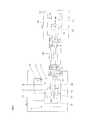
以下、図面を参照して本発明を実施するための最良の形態について説明する。図1は、本発明の一実施の形態によるインターフェイスシステムを説明する図である。図1において、インターフェイスシステムはUSB接続部を有する電子機器で構成される。本実施形態では、USBデバイス10およびUSBホスト50をケーブルを介さずに直接接続し、USBデバイス10からUSBホスト50へ電力を供給(給電)する。 The best mode for carrying out the present invention will be described below with reference to the drawings. FIG. 1 is a diagram for explaining an interface system according to an embodiment of the present invention. In FIG. 1, the interface system is configured by an electronic device having a USB connection unit. In the present embodiment, the
USBデバイス10は、たとえば電子カメラで構成し、USBホスト50は、たとえば無線LANモジュールで構成する。無線LANモジュール50を電子カメラ10に直接接続することにより、電子カメラ10内に蓄積された画像データをパソコンなどを介さずにネットワーク上のサーバなどへ転送することが可能となる。 The
USB(Universal Serial Bus)は、電源用のVBUSラインと、プラス側データ用のD+ラインと、マイナス側データ用のD−ラインと、基準電位用のGNDラインと、デュアルロールデバイスにおいて「ホスト機器」または「デバイス機器」の判別に用いられるIDラインとによって構成されている。デュアルロールデバイスは、USB−OTG(USB On-the-Go)規格に準拠する機器であり、IDラインから検出される電圧レベルによって「ホスト機器」としても「デバイス機器」としても動作する機器をいう。 USB (Universal Serial Bus) is a “host device” in a dual-role device for a VBUS line for power supply, a D + line for positive data, a D- line for negative data, a GND line for reference potential, and a dual-role device. Or it is comprised by the ID line used for discrimination | determination of a "device apparatus". A dual-role device is a device that conforms to the USB-OTG (USB On-the-Go) standard and refers to a device that operates as both a “host device” and a “device device” depending on the voltage level detected from the ID line. .
USB接続された機器間の電力供給はVBUSラインを通して行われる。また、USB接続された機器間の通信は、D+ラインおよびD−ラインによる一対のデータラインを介したシリアル通信で行われる。 Power supply between devices connected via USB is performed through the VBUS line. Communication between devices connected via USB is performed by serial communication via a pair of data lines of the D + line and the D− line.
図1のUSBデバイス10は、制御部12と、デバイスコントローラ13と、電界効果トランジスタ(以降FETと呼ぶ)14と、抵抗器15および20と、ダイオード16および19と、アナログスイッチ17および18と、コネクタRC11とを含み、電池11が装填される。なお、USBデバイス10においてカメラの撮影処理に必要なブロック(撮像光学系、撮像素子、画像処理部、メモリ、操作部材および記録媒体など)については説明を省略する。 1 includes a
電池11は、制御部12、デバイスコントローラ13をはじめとするUSBデバイス10の各ブロックへ電力を供給する。制御部12はマイクロコンピュータを含み、USBデバイス10(本例では電子カメラ)内の各ブロックの動作を制御する。デバイスコントローラ13は、制御部12からの指示を受けてUSBデバイス10が「デバイス機器」として動作するための制御を行う。USBホスト50とのデータ通信は後述するホストコントローラ51によって制御される。USBデバイス10からUSBホスト50へデータを送信する場合でも、USBホスト50がバスの使用権をUSBデバイス10に与えなければ、当該データの送信ができないように構成されている。 The
アナログスイッチ18は、制御部12からの切替制御信号に応じてオン/オフが制御される。具体的には、切替制御信号の論理レベルがHの場合にオンし、切替制御信号の論理レベルがLの場合にオフする。 The
FET14は、アナログスイッチ18の切替状態と、IDラインの電圧レベルとによってオン/オフが制御される。具体的には、アナログスイッチ18がオン時であって、かつIDラインの電圧が所定電圧以下の場合にオンする。反対に、アナログスイッチ18がオフ、またはアナログスイッチ18がオン時であってもIDラインの電圧が所定電圧より高い場合にはオフする。FET14がオンすると、電池11の電力がFET14およびダイオード16を介してコネクタRC11のVBUS端子へ供給される。FET14の代わりに、他のアナログスイッチやリレーなどの切替部材を用いてもよい。ダイオード16は、逆流電流防止用に配設されている、抵抗器15は、FET14のゲート端子を所定電位にするために配設されている。 The FET 14 is controlled to be turned on / off by the switching state of the
アナログスイッチ17は、制御部12からの切替制御信号に応じてオン/オフが制御される。具体的には、切替制御信号の論理レベルがHの場合にオンし、切替制御信号の論理レベルがLの場合にオフする。 The
制御部12は、アナログスイッチ17がオン時に限り、検出ポートPIDによりIDラインの電圧レベルを検出可能に構成される。アナログスイッチ17がオンすると、IDラインが抵抗器20を介して電源ライン(電池11の正極側)と接続(いわゆるプルアップ)されるので、コネクタRC11に何も接続されていない状態におけるIDラインの電圧レベルが所定電圧より高い電圧値になる。これにより、USBデバイス10に他の機器が接続され、当該他の機器でIDラインがGNDラインと接続されているような場合には、制御部12に入力されるIDラインの電圧が変化するので、制御部12はIDラインの電圧レベルの低下を検出することができる。The
一方、アナログスイッチ17がオフされた場合には、IDラインが抵抗器20を介して電源ラインに接続されないため、コネクタRC11に何も接続されていない状態におけるIDラインの電圧レベルが不定になる。この場合は制御部12がIDラインの電圧レベルの低下を検出できない。なお、抵抗器20はプルアップ用の抵抗器であり、ダイオード19はIDラインの逆流電流防止用に配設されている。 On the other hand, when the
コネクタRC11は、ミニBタイプレセプタクル(Mini-Bレセプタクル)で構成される。ミニBタイプレセプタクルは、「デバイス機器」専用のコネクタである。コネクタRC11には、「ホスト機器」または「USBケーブル」が有するミニBタイププラグ(Mini-Bプラグ)が嵌合する。コネクタRC11は、VBUSラインに対応するVBUS端子、D+ラインに対応するD+端子、D−ラインに対応するD−端子、GNDラインに対応するGND端子、IDラインに対応するID端子をそれぞれ含む。 The connector RC11 is composed of a mini-B type receptacle (Mini-B receptacle). The mini-B type receptacle is a connector dedicated to “device equipment”. The connector RC11 is fitted with a mini-B type plug (Mini-B plug) included in the “host device” or “USB cable”. The connector RC11 includes a VBUS terminal corresponding to the VBUS line, a D + terminal corresponding to the D + line, a D− terminal corresponding to the D− line, a GND terminal corresponding to the GND line, and an ID terminal corresponding to the ID line.
USBホスト50は、制御部52と、ホストコントローラ51と、コネクタPL21とを含む。なお、USBホスト50において無線通信処理に必要なブロックは図示を省略している。USBホスト50は電源を有しておらず、USBデバイス10から供給される電力を受電してホストコントローラ51および制御部52へ供給する。 The
制御部52はマイクロコンピュータを含み、USBホスト50(本例では無線LANモジュール)内の各ブロックの動作を制御する。ホストコントローラ51は、制御部52からの指示を受けてUSBホスト50が「ホスト機器」として動作するための制御を行う。ホストコントローラ51の制御により、バスで起こる処理はすべてUSBホスト50から開始される。 The
コネクタPL21は、ミニBタイププラグ(Mini-Bプラグ)で構成される。ミニBタイププラグは、「ホスト機器」専用のコネクタである。コネクタPL21には、「デバイス機器」が有するミニBタイプレセプタクル(Mini-Bレセプタクル)が嵌合する。コネクタPL21は、VBUSラインに対応するVBUS端子、D+ラインに対応するD+端子、D−ラインに対応するD−端子、GNDラインに対応するGND端子、IDラインに対応するID端子をそれぞれ含む。なお、GND端子およびID端子間は、USBホスト50内で接続されている。 Connector PL21 is formed of a mini-B type plug (Mini-B plug). The mini-B type plug is a connector dedicated to the “host device”. The connector PL21 is fitted with a mini-B type receptacle (Mini-B receptacle) included in the “device device”. Connector PL21 includes a VBUS terminal corresponding to the VBUS line, a D + terminal corresponding to the D + line, a D− terminal corresponding to the D− line, a GND terminal corresponding to the GND line, and an ID terminal corresponding to the ID line. The GND terminal and the ID terminal are connected in the
上述したUSBデバイス10およびUSBホスト50は、以下の手順で使用される。
<手順1>USBデバイス10およびUSBホスト50が、コネクタRC11およびコネクタPL21によって接続される。
<手順2>USBデバイス10は、たとえば操作部材を用いたメニュー操作によって無線LANモジュールの使用が許可される。USBデバイス10の制御部12は、無線LANモジュールの使用が許可されると、(a)アナログスイッチ17へ出力する切替制御信号の論理レベルをHレベルにし、アナログスイッチ17をオンに切替える。アナログスイッチ17のオンにより、制御部12はIDラインの電圧レベルの低下を検出可能になる(許可される)。The
<Procedure 1> The
<Procedure 2> The
USBデバイス10の制御部12は、IDラインの電圧レベルの低下を検出すると、(b)アナログスイッチ18へ出力する切替制御信号の論理レベルをHレベルにし、アナログスイッチ18をオンに切替える。アナログスイッチ18のオンにより、FET14のオンが許可される。これにより、FET14のゲート端子に電圧レベルが低下したIDラインが接続されてFET14がオンするので、電池11の電力がVBUSラインを通してUSBデバイス10からUSBホスト50へ供給される。 When the
USBデバイス10の制御部12は、無線LANモジュールの使用が許可されない場合は、アナログスイッチ17へ出力する切替制御信号の論理レベルをLレベルにし、アナログスイッチ17をオフに切替える。制御部12はさらに、IDラインの電圧レベルの電圧低下を検出していない場合はアナログスイッチ18へ出力する切替制御信号の論理レベルをLレベルにし、アナログスイッチ18をオフに切替える。 When the use of the wireless LAN module is not permitted, the
以上説明した実施形態によれば、以下の作用効果が得られる。
(1)USB(Universal Serial Bus)を介してUSBデバイス10およびUSBホスト50間が接続されている状態で、検出したIDラインの電圧に応じてUSBデバイス10からUSBホスト50へVBUSラインを通して電力を供給する場合において、制御部12がIDラインの電圧レベルの変化を検出することを許可する/許可しないを切替えるアナログスイッチ17を設けた。これにより、上記検出を許可しない場合には、想定外の機器がUSBデバイス10に接続されてIDラインの電圧が低下したとしても、当該電圧低下を検知しないようにフェイルセーフの構成とすることができる。According to the embodiment described above, the following effects can be obtained.
(1) In a state where the
(2)アナログスイッチ17がオン時はIDラインを電源(電池11)に抵抗器20を介してプルアップ接続し、アナログスイッチ17がオフ時は上記プルアップ接続をしない。これにより、上記検出を許可しない場合にはIDラインの電圧レベルをHレベルでもLレベルでもないハイインピーダンス状態にすることができる。(2) When the
(3)USB(Universal Serial Bus)を介してUSBデバイス10およびUSBホスト50間が接続されている状態で、検出したIDラインの電圧に応じてUSBデバイス10からUSBホスト50へVBUSラインを通して電力を供給する場合において、電源(電池11)およびVBUSラインを結ぶ電力ラインをオン/オフするFET14と、FET14のオン/オフ切替えを許可する/許可しないを切替えるアナログスイッチ18とを設けた。これにより、上記切替えを許可しない場合には、IDラインの電圧が低下したとしてもFET14がオンしないようにフェイルセーフの構成とすることができる。
(4)アナログスイッチ18がオン時にFET14のゲート端子とFET14に対する切替制御信号とを接続し、アナログスイッチ18がオフ時は上記切替制御信号の接続をしない。これにより、上記FET14の切替えを許可しない場合は、いかなる切替制御信号が発生しようとも確実にFET14のオン(VBUSラインからの電力供給)を止めることができる。(3) In a state where the
(4) The gate terminal of the
(5)アナログスイッチ17を先にオンさせてからアナログスイッチ18をオンさせるようにしたので、IDラインの電圧低下を検出していないにもかかわらずFET14がオンしてしまうという事態を避けることができる。(5) Since the
(6)アナログスイッチ18のオフ時は必ずFET14がオフする構成としたので、USBデバイス10からUSBホスト50へ電力を供給させたくない場合には確実に当該供給を止めることができる。(6) Since the
(7)USBデバイス10は、デュアルロールデバイスとして構成することなく、すなわち、USB−OTG(USB On-the-Go)規格に対応させたコントローラやソフトウェアを搭載することなく、USBデバイス10からUSBホスト50へ電力を供給することできる。これにより、安価なインターフェイスシステムを実現できる。(7) The
(変形例1)
図2は、図1の場合と異なるUSBホスト60が接続される場合を説明する図である。図である。図2において、USBデバイス10はUSBホスト60とUSBケーブル65を介して接続される。図2の例では、USBホスト60は「デバイス機器」に向けて電力を供給(給電)する機能を有する。(Modification 1)
FIG. 2 is a diagram illustrating a case where a
USBデバイス10は、図1の場合と同様なので説明を省略する。なお、図2においては、カメラの撮影処理に必要なブロックについての図示を省略している。USBケーブル65は、方向性を有するケーブルである。USBケーブル65の一端に設けられるコネクタPL42は、ミニBタイププラグ(Mini-Bプラグ)で構成される。ミニBタイププラグは、「デバイス機器」側用のコネクタである。コネクタPL42には、「デバイス機器」が有するミニBタイプレセプタクル(Mini-Bレセプタクル)が嵌合する。 The
USBケーブル65の他端に設けられるコネクタPL41は、Aタイププラグ(Aプラグ)で構成される。Aタイププラグは、「ホスト機器」側用のコネクタである。コネクタPL41には、「ホスト機器」が有するAタイプレセプタクル(Aレセプタクル)が嵌合する。USBケーブル65の両端のコネクタ形状が異なることで、「ホスト機器」同士、「デバイス機器」同士が誤って接続されることが防止される。 The connector PL41 provided at the other end of the
コネクタPL41は、いわゆるフルサイズコネクタであり、端子数は4である。コネクタPL42は、上述したミニタイプコネクタであり、端子数は5である。コネクタPL41にはID端子が含まれていないため、USBケーブル65においてID端子に接続される配線はなく、コネクタPL42に含まれるID端子はオープン(無接続)にされている。 Connector PL41 is a so-called full-size connector, and the number of terminals is four. The connector PL42 is the above-described mini-type connector, and the number of terminals is five. Since the connector PL41 does not include an ID terminal, there is no wiring connected to the ID terminal in the
USBホスト60は、制御部62と、ホストコントローラ61と、コネクタRC31(Aタイプレセプタクル)を有し、電池63が装填される。なお、USBホスト60において無線通信処理に必要なブロックは図示を省略している。USBホスト60は、電池63から供給される電力をホストコントローラ61および制御部62へ供給する。 The
制御部62はマイクロコンピュータを含み、USBホスト60(本例では無線LANモジュール)内の各ブロックの動作を制御する。ホストコントローラ61は、制御部62からの指示を受けてUSBホスト60が「ホスト機器」として動作するための制御を行う。ホストコントローラ61の制御により、バスで起こる処理はすべてUSBホスト60から開始される。 The
コネクタRC31は、Aタイプレセプタクル(Aレセプタクル)で構成される。Aタイプレセプタクルは、「ホスト機器」専用のコネクタである。コネクタRC31には、USBケーブル65が有するコネクタPL41(Aプラグ)が嵌合する。コネクタRC31は、VBUSラインに対応するVBUS端子、D+ラインに対応するD+端子、D−ラインに対応するD−端子、GNDラインに対応するGND端子をそれぞれ含む。 The connector RC31 is composed of an A type receptacle (A receptacle). The A type receptacle is a connector dedicated to the “host device”. A connector PL41 (A plug) included in the
図2の構成によれば、USBデバイス10は、「ホスト機器」からVBUSラインを介して電力が供給されなくても自らの電源(電池11)によって動作できる。制御部12は、初期状態として少なくともアナログスイッチ18をオフさせておけばFET14がオンしないので、VBUSラインを通してUSBデバイス10からUSBホスト60へ電力供給をしない。これにより、VBUSラインを通してUSBホスト60からUSBデバイス10へ供給される電源とUSBデバイス10側の電源とが干渉することを防止できる。 According to the configuration of FIG. 2, the
(変形例2)
アナログスイッチ17およびアナログスイッチ18は、いずれか一方または両方をメカニカルスイッチで構成してもよい。この場合には、ユーザがUSBデバイス10に無線LANモジュールの使用を許可する場合は、メカニカルスイッチがオン操作される。反対に、USBデバイス10に無線LANモジュールの使用を許可しない場合にはメカニカルスイッチがオフ操作される。(Modification 2)
Either one or both of the
(変形例3)
FET14のゲート端子へ入力する切替制御信号は、ID端子を通してUSBデバイス10の外部から入力される信号を用いる代わりに、制御部12が発するように構成してもよい。この場合の制御部12は、USBデバイス10の外部から入力されるIDラインの電圧レベルの低下を検出すると、FET14のゲート端子へ入力させるための切替制御信号としてLレベルの信号を出力する。制御部12はまた、IDラインの電圧レベルの低下を検出しない場合は、FET14の切替制御信号としてHレベルの信号を出力する。(Modification 3)
The switching control signal input to the gate terminal of the
(変形例4)
スイッチ17およびスイッチ18を両方備える例を説明したが、スイッチ17およびスイッチ18のうち、いずれか一方のみを有する構成にしてもよい。(Modification 4)
Although an example in which both the
(変形例5)
USBデバイス10からUSBホスト50へ電力供給する例を説明したが、検出したIDラインの電圧に応じてUSBホスト50がUSBデバイス10へVBUSラインを通して電力を供給する場合にも本発明を適用してよい。(Modification 5)
Although an example in which power is supplied from the
以上の説明では、USBデバイス10として電子カメラを例にあげて説明したが、携帯電話機やPDAなどの携帯型電子機器として構成してもよい。 In the above description, an electronic camera has been described as an example of the
上述した説明では、USBホスト50として無線LANモジュールを例にあげて説明したが、チューナーやGPS受信部などのモジュールとして構成してもよい。 In the above description, the wireless LAN module has been described as an example of the
以上の説明はあくまで一例であり、上記の実施形態の構成に何ら限定されるものではない。 The above description is merely an example, and is not limited to the configuration of the above embodiment.
10…USBデバイス
11…電池
12、52、62…制御部
13…デバイスコントローラ
14…FET
15、20…抵抗器
17、18…アナログスイッチ
50、60…USBホスト
51、61…ホストコントローラDESCRIPTION OF
15, 20 ...
Claims (5)
Translated fromJapanese前記USB接続部の識別用端子の電圧を検出する電圧検出部と、A voltage detection unit for detecting the voltage of the identification terminal of the USB connection unit;
前記USB接続部の給電用端子に電池からの電力を供給可能とするか否かを切り替える第1切替部と、A first switching unit that switches whether or not power from a battery can be supplied to the power supply terminal of the USB connection unit;
前記第1切替部の制御用端子と前記識別用端子との間に配置され、前記電圧検出部により検出された前記識別用端子の電圧に応じて前記第1切替部による切り替えを許可するか否かを制御する第2切替部とを備え、Whether to allow switching by the first switching unit according to the voltage of the identification terminal, which is arranged between the control terminal of the first switching unit and the identification terminal and detected by the voltage detection unit A second switching unit for controlling
前記第1切替部による切り替えが前記第2切替部により許可されている場合、前記識別用端子を介して前記電子機器に入力された切替制御信号が前記第2切替部を介して前記第1切替部の前記制御用端子に入力されたときは、前記第1切替部は、前記電池からの電力を前記給電用端子に供給可能とし、前記切替制御信号が前記切替部を介して前記第1切替部の前記制御用端子に入力されないときは、前記第1切替部は、前記電池からの電力を前記給電用端子に供給可能とせず、When switching by the first switching unit is permitted by the second switching unit, a switching control signal input to the electronic device via the identification terminal is transmitted to the first switching unit via the second switching unit. When the signal is input to the control terminal, the first switching unit can supply power from the battery to the power feeding terminal, and the switching control signal is transmitted to the first switching unit via the switching unit. The first switching unit does not allow the power from the battery to be supplied to the power supply terminal,
前記第1切替部による切り替えが前記第2切替部により許可されていない場合、前記切替制御信号の前記第1切替部への入力は前記第2切替部により遮断され、前記第1切替部は、前記電池からの電力を前記給電用端子に供給可能としないことWhen the switching by the first switching unit is not permitted by the second switching unit, the input of the switching control signal to the first switching unit is blocked by the second switching unit, the first switching unit, The power from the battery cannot be supplied to the power supply terminal.
を特徴とする電子機器。Electronic equipment characterized by
前記切替制御信号は、前記識別用端子の電圧レベルに応じた信号であることThe switching control signal is a signal corresponding to the voltage level of the identification terminal.
を特徴とする電子機器。Electronic equipment characterized by
前記第1切替部による切り替えが前記第2切替部により許可されている場合、前記識別用端子の電圧が所定電圧以下のときは、前記第1切替部は、前記電池からの電力を前記給電用端子に供給可能とし、前記識別用端子の電圧が前記所定電圧よりも高いときは、前記第1切替部は、前記電池からの電力を前記給電用端子に供給可能としないことWhen switching by the first switching unit is permitted by the second switching unit, when the voltage of the identification terminal is equal to or lower than a predetermined voltage, the first switching unit uses power from the battery for the power supply. When the voltage of the identification terminal is higher than the predetermined voltage, the first switching unit is not allowed to supply power from the battery to the power supply terminal.
を特徴とする電子機器。Electronic equipment characterized by
前記電圧検出部による前記識別用端子の電圧検出を可能とするか否かを制御する第3切替部を更に備えることA third switching unit for controlling whether or not the voltage detection unit can detect the voltage of the identification terminal;
を特徴とする電子機器。Electronic equipment characterized by
前記第3切替部は、ユーザ操作に応じて、前記電圧検出部による前記識別用端子の電圧検出を可能するか否かを切り替えることThe third switching unit switches whether the voltage detection unit can detect the voltage of the identification terminal according to a user operation.
を特徴とする電子機器。Electronic equipment characterized by
Priority Applications (4)
| Application Number | Priority Date | Filing Date | Title |
|---|---|---|---|
| JP2006347361AJP4961999B2 (en) | 2006-12-25 | 2006-12-25 | Electronics |
| US12/000,762US20080150512A1 (en) | 2006-12-25 | 2007-12-17 | Electronic device |
| US13/252,514US20120030485A1 (en) | 2006-12-25 | 2011-10-04 | Electronic device |
| US13/523,168US8539266B2 (en) | 2006-12-25 | 2012-06-14 | Electronic device |
Applications Claiming Priority (1)
| Application Number | Priority Date | Filing Date | Title |
|---|---|---|---|
| JP2006347361AJP4961999B2 (en) | 2006-12-25 | 2006-12-25 | Electronics |
Publications (2)
| Publication Number | Publication Date |
|---|---|
| JP2008158840A JP2008158840A (en) | 2008-07-10 |
| JP4961999B2true JP4961999B2 (en) | 2012-06-27 |
Family
ID=39541869
Family Applications (1)
| Application Number | Title | Priority Date | Filing Date |
|---|---|---|---|
| JP2006347361AActiveJP4961999B2 (en) | 2006-12-25 | 2006-12-25 | Electronics |
Country Status (2)
| Country | Link |
|---|---|
| US (3) | US20080150512A1 (en) |
| JP (1) | JP4961999B2 (en) |
Families Citing this family (49)
| Publication number | Priority date | Publication date | Assignee | Title |
|---|---|---|---|---|
| JP5034466B2 (en)* | 2006-12-05 | 2012-09-26 | 株式会社ニコン | Device equipment, host equipment and interface system |
| JP4961999B2 (en) | 2006-12-25 | 2012-06-27 | 株式会社ニコン | Electronics |
| US8230126B2 (en)* | 2009-10-27 | 2012-07-24 | Fairchild Semiconductor Corporation | Camera shutter control through a USB port or audio/video port |
| US8244927B2 (en) | 2009-10-27 | 2012-08-14 | Fairchild Semiconductor Corporation | Method of detecting accessories on an audio jack |
| GB2477504B (en)* | 2010-02-03 | 2017-07-26 | Lm Tech Ltd | A device arranged to use an electromagnetic link to replicate a serial port |
| EP2390969A1 (en)* | 2010-05-26 | 2011-11-30 | Samsung Electronics Co., Ltd. | Connector and interface device |
| US8817994B2 (en) | 2010-07-23 | 2014-08-26 | Fairchild Semiconductor Corporation | Audio jack reset |
| JP5812502B2 (en)* | 2010-08-24 | 2015-11-17 | マーベル ワールド トレード リミテッド | Device interface and apparatus |
| US9229833B2 (en)* | 2011-01-28 | 2016-01-05 | Fairchild Semiconductor Corporation | Successive approximation resistor detection |
| CN102692986B (en) | 2011-02-14 | 2017-04-12 | 株式会社尼康 | Electronic appliance, connecting appliance, electronic appliance system and method |
| JP5382045B2 (en)* | 2011-03-31 | 2014-01-08 | 株式会社ニコン | Electronic device, electronic device system and program |
| JP5293756B2 (en)* | 2011-02-14 | 2013-09-18 | 株式会社ニコン | Interface system and dual-role device |
| US8788852B2 (en)* | 2011-07-01 | 2014-07-22 | Intel Corporation | System and method for providing power through a reverse local data transfer connection |
| US9497559B2 (en) | 2011-07-22 | 2016-11-15 | Fairchild Semiconductor Corporation | MIC/GND detection and automatic switch |
| JP2013090006A (en) | 2011-10-13 | 2013-05-13 | Nikon Corp | Electronic apparatus and program |
| TWI578147B (en)* | 2011-11-30 | 2017-04-11 | 緯創資通股份有限公司 | Power consumption control method for an electronic system and electronic system thereof |
| US8880752B2 (en)* | 2011-12-15 | 2014-11-04 | Motorola Mobility Llc | Customizing and/or multiplexing universal serial bus pins |
| JPWO2013168289A1 (en)* | 2012-05-11 | 2015-12-24 | 富士通株式会社 | Electronic device and control method thereof |
| US9497544B2 (en) | 2012-07-02 | 2016-11-15 | Qualcomm Incorporated | Systems and methods for surround sound echo reduction |
| KR102158288B1 (en)* | 2012-07-09 | 2020-09-21 | 삼성전자주식회사 | Method for charging battery and an electronic device thereof |
| US9060228B2 (en) | 2012-08-03 | 2015-06-16 | Fairchild Semiconductor Corporation | Accessory detection circuit with improved functionality |
| TWI467886B (en)* | 2012-08-20 | 2015-01-01 | Quanta Comp Inc | Electronic devices and electronic systems |
| KR102044898B1 (en)* | 2012-12-03 | 2019-11-14 | 휴렛-팩커드 디벨롭먼트 컴퍼니, 엘.피. | Method for sensing connection of USB device and image forming apparatus performing the same |
| TWI501085B (en)* | 2013-05-17 | 2015-09-21 | Primax Electronics Ltd | Usb interface detection device |
| KR20150006559A (en)* | 2013-07-09 | 2015-01-19 | 삼성전자주식회사 | Universal serial bus apparatus and electric device including the universal serial bus apparatus |
| US9507398B2 (en)* | 2014-02-28 | 2016-11-29 | Infineon Technologies Austria Ag | Communication over identification line |
| TWI518515B (en)* | 2014-05-05 | 2016-01-21 | 新唐科技股份有限公司 | Control chip and connection module utilizing the same |
| JP5986145B2 (en)* | 2014-07-02 | 2016-09-06 | レノボ・シンガポール・プライベート・リミテッド | Portable devices, cable assemblies and USB systems |
| CN104320115A (en)* | 2014-11-06 | 2015-01-28 | 贸联电子(昆山)有限公司 | USB OTG module |
| WO2016101215A1 (en)* | 2014-12-25 | 2016-06-30 | 华为技术有限公司 | System and device for identifying usb otg device |
| US9984030B2 (en) | 2014-12-31 | 2018-05-29 | Xiaomi Inc. | Electronic device and data transmission system |
| CN104615569A (en)* | 2014-12-31 | 2015-05-13 | 小米科技有限责任公司 | Electronic equipment and data transmission system |
| CN105988545A (en)* | 2015-02-09 | 2016-10-05 | 鸿富锦精密工业(武汉)有限公司 | Electronic device and power supply interface |
| KR102386551B1 (en)* | 2015-07-27 | 2022-04-15 | 삼성전자주식회사 | Connecting Device and Method for Recognizing Device |
| CN106445856B (en) | 2015-08-07 | 2019-05-14 | 小米科技有限责任公司 | Interface circuit, state switching method and device |
| CN105228044A (en)* | 2015-09-28 | 2016-01-06 | 惠州Tcl移动通信有限公司 | A kind of harmless tonequality earphone |
| DE102015116800B3 (en)* | 2015-10-02 | 2016-12-29 | Beckhoff Automation Gmbh | Input / output module for a bus system |
| DE102015116802B3 (en)* | 2015-10-02 | 2016-12-29 | Beckhoff Automation Gmbh | bus system |
| JP6021208B1 (en)* | 2015-10-29 | 2016-11-09 | Necプラットフォームズ株式会社 | Incorrect connection prevention device and erroneous connection prevention method |
| CN106684955B (en)* | 2015-11-11 | 2019-10-15 | 小米科技有限责任公司 | Charger, electronic equipment and charging method |
| JP6661342B2 (en)* | 2015-11-26 | 2020-03-11 | Dynabook株式会社 | Port connection circuit, port connection control method, electronic equipment |
| CN106897239A (en) | 2015-12-21 | 2017-06-27 | 小米科技有限责任公司 | state switching method and device |
| EP3270584B1 (en)* | 2016-07-12 | 2020-09-02 | InterDigital CE Patent Holdings | Galvanic isolated device and corresponding method and system |
| US10573999B2 (en)* | 2016-11-22 | 2020-02-25 | Haoxiang Electric Energy (Kunshan) Co., Ltd. | Power communication electrical connector |
| CN108628787B (en)* | 2017-03-22 | 2023-02-07 | 鸿富锦精密工业(武汉)有限公司 | Interface control circuit |
| JP6878102B2 (en)* | 2017-04-07 | 2021-05-26 | キヤノン株式会社 | Electronic devices and their control methods |
| US10837934B2 (en) | 2018-03-28 | 2020-11-17 | Samsung Electronics Co., Ltd. | Water detection circuit, electronic device including the same, and water detection method |
| WO2019233389A1 (en)* | 2018-06-04 | 2019-12-12 | 惠州市睿普斯林智能科技有限公司 | Sofa usb socket |
| US11777237B1 (en)* | 2022-05-24 | 2023-10-03 | Inventus Power, Inc. | Disconnecting power from external USB connectors of conformable wearable battery packs in the presence of conducting fluids |
Family Cites Families (22)
| Publication number | Priority date | Publication date | Assignee | Title |
|---|---|---|---|---|
| JPS5396423A (en)* | 1977-02-01 | 1978-08-23 | Mitsubishi Electric Corp | Control system for induction motor |
| US6072304A (en)* | 1999-07-21 | 2000-06-06 | Regent Lighting Corporation | Circuit and method for triggering a thyristor |
| US7028126B1 (en)* | 2000-09-21 | 2006-04-11 | Ping Liang | Universal serial bus for mobile devices having expansion modules |
| JP3558059B2 (en) | 2001-08-10 | 2004-08-25 | セイコーエプソン株式会社 | Power supply control circuit and electronic equipment |
| JP3654274B2 (en)* | 2002-08-30 | 2005-06-02 | セイコーエプソン株式会社 | Data transfer control device, electronic device, and power supply switching method |
| WO2004036401A2 (en)* | 2002-10-18 | 2004-04-29 | Thomson Licensing S.A. | Bus controlled power switch |
| JP3959374B2 (en)* | 2003-06-30 | 2007-08-15 | Tdk株式会社 | USB interface system |
| WO2005018219A2 (en)* | 2003-08-15 | 2005-02-24 | Dice America, Inc. | Apparatus for communicating over a network images captured by a digital camera |
| JP4504666B2 (en)* | 2003-12-09 | 2010-07-14 | 株式会社アイ・オー・データ機器 | Peripheral device and reconnection program |
| JP2006001063A (en)* | 2004-06-16 | 2006-01-05 | Fuji Photo Film Co Ltd | Direct print system |
| JP2006018466A (en)* | 2004-06-30 | 2006-01-19 | Canon Inc | Electronic apparatus and power supply control method therefor |
| JP2006099354A (en)* | 2004-09-29 | 2006-04-13 | Matsushita Electric Ind Co Ltd | Data transfer control device and data transfer control method |
| US7343147B2 (en)* | 2005-04-04 | 2008-03-11 | Freescale Semiconductor, Inc. | Method and apparatus for powering and loading software into a battery-less electronic device |
| JP2007043490A (en)* | 2005-08-03 | 2007-02-15 | Canon Inc | Camera cradle device and system thereof |
| TWI383289B (en)* | 2005-09-05 | 2013-01-21 | Hon Hai Prec Ind Co Ltd | Controller and method for on-off switching of power supply |
| US7589536B2 (en)* | 2007-01-05 | 2009-09-15 | Apple Inc. | Systems and methods for determining the configuration of electronic connections |
| US8035368B2 (en)* | 2006-02-13 | 2011-10-11 | Freescale Semiconductor, Inc. | Integrated circuit, universal serial bus on-the-go power source and methods for use therewith |
| US7899418B2 (en)* | 2006-02-22 | 2011-03-01 | Fujifilm Corporation | Mobile device and wireless communication apparatus |
| JP4961999B2 (en) | 2006-12-25 | 2012-06-27 | 株式会社ニコン | Electronics |
| US20080265838A1 (en)* | 2007-04-24 | 2008-10-30 | Saurabh Garg | Battery charging using a USB-ID pin of a USB interface |
| WO2009062551A1 (en)* | 2007-11-15 | 2009-05-22 | Nokia Corporation | Power connection between serial interfaces |
| US8230126B2 (en)* | 2009-10-27 | 2012-07-24 | Fairchild Semiconductor Corporation | Camera shutter control through a USB port or audio/video port |
- 2006
- 2006-12-25JPJP2006347361Apatent/JP4961999B2/enactiveActive
- 2007
- 2007-12-17USUS12/000,762patent/US20080150512A1/ennot_activeAbandoned
- 2011
- 2011-10-04USUS13/252,514patent/US20120030485A1/ennot_activeAbandoned
- 2012
- 2012-06-14USUS13/523,168patent/US8539266B2/enactiveActive
Also Published As
| Publication number | Publication date |
|---|---|
| US20120254638A1 (en) | 2012-10-04 |
| US8539266B2 (en) | 2013-09-17 |
| JP2008158840A (en) | 2008-07-10 |
| US20080150512A1 (en) | 2008-06-26 |
| US20120030485A1 (en) | 2012-02-02 |
Similar Documents
| Publication | Publication Date | Title |
|---|---|---|
| JP4961999B2 (en) | Electronics | |
| JP5034466B2 (en) | Device equipment, host equipment and interface system | |
| KR100775992B1 (en) | Device operable as a host | |
| JP5283719B2 (en) | Electronic equipment and electronic equipment system | |
| US7886104B2 (en) | Detachable adapter and portable system | |
| JP3610424B2 (en) | Electronic equipment and interface circuit | |
| KR20040102341A (en) | Method and apparatus for handling a charging state in a mobile electronic device | |
| JP2020008898A (en) | Electronic equipment | |
| JP5058083B2 (en) | Interface device | |
| KR20190047526A (en) | A method for performing communication via input output interface and a method thereof | |
| KR20190102706A (en) | Electronic Device which operates by External Power | |
| US20060145666A1 (en) | Device and method for charging an OTG portable device | |
| US7464206B2 (en) | Semiconductor device and method of connecting the same | |
| JP2002116853A (en) | Usb mounted electronic equipment and use cable to be used therefor | |
| US11322970B2 (en) | Device with power-off charging capability | |
| JP5251317B2 (en) | Device equipment, host equipment and interface system | |
| US20030163614A1 (en) | Device with interface recognizing ability | |
| CN108513656B (en) | Control method, USB system and electronic device | |
| JP2002163051A (en) | Electronic equipment, USB connector mechanism, and USB device connection cable | |
| CN102544952B (en) | Transducer and the imaging device be connected with transducer | |
| KR100700532B1 (en) | How to recognize the connector on the universal serial bus port and the universal serial bus adapter | |
| JP2007102444A (en) | Electronic device, control method and control program for electronic device | |
| JP2003223249A (en) | Voltage protection circuit | |
| US10235311B2 (en) | Data acquisition system, electronic device, and data acquisition terminal | |
| JP2015215643A (en) | Electronic equipment and recovery control method from power saving state |
Legal Events
| Date | Code | Title | Description |
|---|---|---|---|
| A621 | Written request for application examination | Free format text:JAPANESE INTERMEDIATE CODE: A621 Effective date:20091201 | |
| A521 | Request for written amendment filed | Free format text:JAPANESE INTERMEDIATE CODE: A523 Effective date:20101130 | |
| A977 | Report on retrieval | Free format text:JAPANESE INTERMEDIATE CODE: A971007 Effective date:20110418 | |
| A131 | Notification of reasons for refusal | Free format text:JAPANESE INTERMEDIATE CODE: A131 Effective date:20110531 | |
| A521 | Request for written amendment filed | Free format text:JAPANESE INTERMEDIATE CODE: A523 Effective date:20110801 | |
| RD02 | Notification of acceptance of power of attorney | Free format text:JAPANESE INTERMEDIATE CODE: A7422 Effective date:20110801 | |
| TRDD | Decision of grant or rejection written | ||
| A01 | Written decision to grant a patent or to grant a registration (utility model) | Free format text:JAPANESE INTERMEDIATE CODE: A01 Effective date:20120228 | |
| A01 | Written decision to grant a patent or to grant a registration (utility model) | Free format text:JAPANESE INTERMEDIATE CODE: A01 | |
| A61 | First payment of annual fees (during grant procedure) | Free format text:JAPANESE INTERMEDIATE CODE: A61 Effective date:20120312 | |
| R150 | Certificate of patent or registration of utility model | Ref document number:4961999 Country of ref document:JP Free format text:JAPANESE INTERMEDIATE CODE: R150 Free format text:JAPANESE INTERMEDIATE CODE: R150 | |
| FPAY | Renewal fee payment (event date is renewal date of database) | Free format text:PAYMENT UNTIL: 20150406 Year of fee payment:3 | |
| FPAY | Renewal fee payment (event date is renewal date of database) | Free format text:PAYMENT UNTIL: 20150406 Year of fee payment:3 | |
| R250 | Receipt of annual fees | Free format text:JAPANESE INTERMEDIATE CODE: R250 | |
| R250 | Receipt of annual fees | Free format text:JAPANESE INTERMEDIATE CODE: R250 | |
| R250 | Receipt of annual fees | Free format text:JAPANESE INTERMEDIATE CODE: R250 | |
| R250 | Receipt of annual fees | Free format text:JAPANESE INTERMEDIATE CODE: R250 | |
| R250 | Receipt of annual fees | Free format text:JAPANESE INTERMEDIATE CODE: R250 | |
| R250 | Receipt of annual fees | Free format text:JAPANESE INTERMEDIATE CODE: R250 |