JP4956593B2 - Memory system - Google Patents
Memory systemDownload PDFInfo
- Publication number
- JP4956593B2 JP4956593B2JP2009207387AJP2009207387AJP4956593B2JP 4956593 B2JP4956593 B2JP 4956593B2JP 2009207387 AJP2009207387 AJP 2009207387AJP 2009207387 AJP2009207387 AJP 2009207387AJP 4956593 B2JP4956593 B2JP 4956593B2
- Authority
- JP
- Japan
- Prior art keywords
- page
- block
- logical
- memory
- pages
- Prior art date
- Legal status (The legal status is an assumption and is not a legal conclusion. Google has not performed a legal analysis and makes no representation as to the accuracy of the status listed.)
- Expired - Fee Related
Links
Images


Classifications
- G—PHYSICS
- G06—COMPUTING OR CALCULATING; COUNTING
- G06F—ELECTRIC DIGITAL DATA PROCESSING
- G06F12/00—Accessing, addressing or allocating within memory systems or architectures
- G06F12/02—Addressing or allocation; Relocation
- G06F12/06—Addressing a physical block of locations, e.g. base addressing, module addressing, memory dedication
- G06F12/0607—Interleaved addressing
- G—PHYSICS
- G06—COMPUTING OR CALCULATING; COUNTING
- G06F—ELECTRIC DIGITAL DATA PROCESSING
- G06F12/00—Accessing, addressing or allocating within memory systems or architectures
- G06F12/02—Addressing or allocation; Relocation
- G06F12/0223—User address space allocation, e.g. contiguous or non contiguous base addressing
- G06F12/023—Free address space management
- G06F12/0238—Memory management in non-volatile memory, e.g. resistive RAM or ferroelectric memory
- G06F12/0246—Memory management in non-volatile memory, e.g. resistive RAM or ferroelectric memory in block erasable memory, e.g. flash memory
- G—PHYSICS
- G06—COMPUTING OR CALCULATING; COUNTING
- G06F—ELECTRIC DIGITAL DATA PROCESSING
- G06F2212/00—Indexing scheme relating to accessing, addressing or allocation within memory systems or architectures
- G06F2212/72—Details relating to flash memory management
- G06F2212/7202—Allocation control and policies
- G—PHYSICS
- G06—COMPUTING OR CALCULATING; COUNTING
- G06F—ELECTRIC DIGITAL DATA PROCESSING
- G06F2212/00—Indexing scheme relating to accessing, addressing or allocation within memory systems or architectures
- G06F2212/72—Details relating to flash memory management
- G06F2212/7208—Multiple device management, e.g. distributing data over multiple flash devices
Landscapes
- Engineering & Computer Science (AREA)
- Theoretical Computer Science (AREA)
- Physics & Mathematics (AREA)
- General Engineering & Computer Science (AREA)
- General Physics & Mathematics (AREA)
- Read Only Memory (AREA)
- Memory System (AREA)
- Techniques For Improving Reliability Of Storages (AREA)
Description
Translated fromJapanese本発明は、多値(multi-level)フラッシュメモリのデータ書き込み技術に関する。 The present invention relates to a data writing technique for a multi-level flash memory.
フラッシュメモリ、特に、NANDフラッシュメモリは、ストレージメモリとして、メモリカード、SSD(solid state drive)など、様々な分野に適用され始めている。これらの分野において、フラッシュメモリシステムを構成する場合、データ書き込み速度の高速化が一つの重要な課題となっている。 Flash memories, particularly NAND flash memories, are beginning to be applied as storage memories in various fields such as memory cards and SSDs (solid state drives). In these fields, when configuring a flash memory system, an increase in data writing speed is an important issue.
ところで、データ転送速度の向上を図る技術としてインターリーブ(interleaving)動作が知られている(例えば、特許文献1〜4を参照)。従って、この技術をフラッシュメモリに適用すれば、データ書き込み速度の高速化という課題を解決できる可能性がある。 Incidentally, an interleaving operation is known as a technique for improving the data transfer rate (see, for example,
しかし、フラッシュメモリは、メモリセル(フィジカルページ)に対してデータの上書きができない、という特有のデータ書き込み方式を有する。即ち、データの上書き時には、オールドブロックの撤収を行い、ニューブロックにデータを書き直す必要がある。 However, the flash memory has a unique data writing method in which data cannot be overwritten on a memory cell (physical page). That is, when overwriting data, it is necessary to remove the old block and rewrite the data in the new block.
従って、データ書き込み速度の高速化は、このようなフラッシュメモリのデータ書き込み方式にマッチしたインターリーブ動作を開発することにより実現される。 Therefore, an increase in data writing speed can be realized by developing an interleave operation that matches such a data writing method of the flash memory.
本発明は、フラッシュメモリに対する高速書き込みをインターリーブ動作により実現するためのメモリシステムを提案する。 The present invention proposes a memory system for realizing high-speed writing to a flash memory by an interleave operation.
本発明の例に係わるメモリシステムは、第1テンポラリメモリと第1ブロックとを有する第1メモリチップと、第2テンポラリメモリと第2ブロックとを有する第2メモリチップと、前記第1及び第2メモリチップに対する複数個のロジカルページの書き込みを制御するメモリコントローラとを備える。前記第1及び第2メモリチップは、それぞれ、1つのメモリセルにn(nは、2以上の自然数)ビットを記憶する多値フラッシュメモリである。前記第1及び第2ブロックは、それぞれ、複数のフィジカルページから構成され、前記書き込みは、最下位のフィジカルページから最上位のフィジカルページに向かってフィジカルページごとに行われる。前記最下位のフィジカルページは、書き込み時間が最も短い下位ページを含み、前記最上位のフィジカルページは、書き込み時間が最も長い上位ページを含み、前記最下位のフィジカルページ及び前記最上位のフィジカルページを除く残りの複数のフィジカルページの各々は、下位ページ、(n−2)個の中位ページ及び上位ページからなる第1単位である。前記メモリコントローラは、前記第1テンポラリメモリと前記第1ブロック内の最下位のフィジカルページとからなる前記第1単位のページ数と同じページ数を有する第2単位、前記第2テンポラリメモリと前記第2ブロック内の最下位のフィジカルページとからなる前記第1単位のページ数と同じページ数を有する第3単位、前記第1ブロック内の前記第1単位及び前記第2ブロック内の前記第1単位の順番で、インターリーブ動作による前記複数個のロジカルページの書き込みを行う。A memory system according to an example of the present invention includes a first memory chip having a first temporary memory and a first block, a second memory chip having a second temporary memory and a second block, and the first and second memory chips. And a memory controller that controls writing of aplurality of logical pages to the memory chip. Each of the first and second memory chips is a multi-level flash memory that stores n (n is a natural number of 2 or more) bits in one memory cell. Each of the first and second blocks is composed of a plurality of physical pages, and the writing is performed for each physical page from the lowest physical page to the highest physical page. The lowest physical page includes a lower page having the shortest write time, and the uppermost physical page includes an upper page having the longest write time, and includes the lowest physical page and the highest physical page.Each of the remaining plurality of physical pages is a first unit including a lower page, (n−2) middle pages, and an upper page. The memory controller, a second unit having the same number of pages as the number of pages of the first unitcomprising a lowest physical pages of the first temporary memory and the firstblock, the said second temporary memory first the third unit having the same number of pages as the number of pages of the first unitcomprising a lowest physical pages in the twoblocks, the first unit and the first unit of the second block of the first block In this order, theplurality of logical pagesare written by the interleave operation.
本発明によれば、フラッシュメモリに対する高速書き込みをインターリーブ動作により実現することができる。 According to the present invention, high-speed writing to a flash memory can be realized by an interleave operation.
以下、図面を参照しながら、本発明の例を実施するための最良の形態について詳細に説明する。 The best mode for carrying out an example of the present invention will be described below in detail with reference to the drawings.
1. 基本構成
本発明の例では、フラッシュメモリに対する高速書き込みをインターリーブ動作により実現するため、以下の構成を採用する。1. Basic configuration
In the example of the present invention, the following configuration is adopted in order to realize high-speed writing to the flash memory by an interleave operation.
まず、フラッシュチップ(メモリチップ)は、1つのメモリセルにn(nは、2以上の自然数)ビットを記憶する多値フラッシュメモリである。また、フラッシュチップは、複数のブロック(メモリブロック)を有し、複数のブロックは、それぞれ、複数のフィジカルページから構成される。 First, a flash chip (memory chip) is a multi-level flash memory that stores n (n is a natural number of 2 or more) bits in one memory cell. Further, the flash chip has a plurality of blocks (memory blocks), and each of the plurality of blocks includes a plurality of physical pages.
ここで、ブロックとは、データの記憶エリアとなるメモリセルアレイを複数に区分したときの一区分のことである。また、ページとは、ブロックを複数に区分したときの一区分のことである。従って、ページサイズは、ブロックサイズよりも小さい。 Here, the block is a section when the memory cell array serving as a data storage area is divided into a plurality of sections. A page is a division when a block is divided into a plurality of blocks. Therefore, the page size is smaller than the block size.
これらの文言は、特に、NANDフラッシュメモリで使用されるが、本発明は、NANDフラッシュメモリに限定されるものではない。 These terms are used particularly in the NAND flash memory, but the present invention is not limited to the NAND flash memory.
書き込みは、最下位のフィジカルページから最上位のフィジカルページに向かってフィジカルページごとに行われる。 Writing is performed for each physical page from the lowest physical page to the highest physical page.
最下位のフィジカルページは、書き込み時間が最も短い下位ページを含み、最上位のフィジカルページは、書き込み時間が最も長い上位ページを含む。最下位のフィジカルページ及び最上位のフィジカルページを除く残りの複数のフィジカルページは、下位ページ、(n−2)個の中位ページ及び上位ページからなる第1単位の繰り返しである。 The lowest physical page includes the lower page having the shortest write time, and the highest physical page includes the upper page having the longest write time. A plurality of remaining physical pages excluding the lowest physical page and the highest physical page are repetitions of a first unit including a lower page, (n-2) middle pages, and an upper page.
このような前提の下、本発明の例では、ロジカルページの初期書き込み時及び上書き時に、それぞれ、ロジカルページを一時的に記憶するテンポラリメモリを用意する。 Under such a premise, in the example of the present invention, a temporary memory for temporarily storing a logical page is prepared when the logical page is initially written and overwritten.
ここで、ロジカルページとは、ホストが指定するページのことであり、フィジカルページとは、フラッシュチップの内部で実際に指定されるページのことである。 Here, the logical page is a page designated by the host, and the physical page is a page actually designated within the flash chip.
また、テンポラリメモリは、例えば、フラッシュチップ内のブロックの書き込み時間が最も短い下位ページ、フラッシュチップ内のページバッファなどである。 The temporary memory is, for example, a lower page having the shortest writing time of a block in the flash chip, a page buffer in the flash chip, or the like.
そして、インターリーブ動作によるロジカルページの書き込みは、例えば、第1フラッシュチップ内のテンポラリメモリとブロックの最下位のフィジカルページとにより第1単位のページ数と同じページ数を有する第2単位を形成し、第2フラッシュチップ内のテンポラリメモリとブロックの最下位のフィジカルページとにより第1単位のページ数と同じページ数を有する第3単位を形成し、第2単位、第3単位、第1フラッシュチップ内の第1単位及び第2フラッシュチップ内の第1単位の順番で行う。 Then, the logical page writing by the interleave operation forms, for example, a second unit having the same page number as the first unit page number by the temporary memory in the first flash chip and the lowest physical page of the block, The temporary unit in the second flash chip and the lowest physical page of the block form a third unit having the same number of pages as the first unit, and the second unit, the third unit, and the first flash chip. In the order of the first unit and the first unit in the second flash chip.
第2単位及び第3単位は、ページシフト動作によるロジカルページの上書きを、いずれのロジカルページから繰り返し行っても、同一のフラッシュチップ内でのロジカルページの順番を崩すことなく、ロジカルページのデータ移動を同一のフラッシュチップ内のみで行うために採用された構成要件である。 The second unit and the third unit move the logical page data without changing the order of the logical pages in the same flash chip, regardless of which logical page is repeatedly overwritten by the page shift operation. This is a configuration requirement that is adopted in order to perform only in the same flash chip.
例えば、4値の場合、インターリーブ動作によるニューブロックに対するロジカルページの書き込みは、2個のロジカルページをペアとして、以下の順番で行う。 For example, in the case of four values, the writing of the logical page to the new block by the interleave operation is performed in the following order with two logical pages as a pair.
A. 第1フラッシュチップ内の第2単位(2ページ)
テンポラリメモリ→最下位のフィジカルページ(下位ページ)
B. 第2フラッシュチップ内の第3単位(2ページ)
テンポラリメモリ→最下位のフィジカルページ(下位ページ)
C. 第1フラッシュチップ内の第1単位(2ページ)
下位ページ→上位ページ
D. 第2フラッシュチップ内の第1単位(2ページ)
下位ページ→上位ページ
E. C.とD.の繰り返し
F. テンポラリメモリに書き込まれたロジカルページのコピー
第1フラッシュメモリ内のテンポラリメモリに書き込まれたロジカルページは、第1フラッシュメモリ内のニューブロックの最上位のフィジカルページ(上位ページ)にコピーされ、第2フラッシュメモリ内のテンポラリメモリに書き込まれたロジカルページは、第2フラッシュメモリ内のニューブロックの最上位のフィジカルページ(上位ページ)にコピーされる。A. Second unit (2 pages) in the first flash chip
Temporary memory → lowest physical page (lower page)
B. 3rd unit in 2nd flash chip (2 pages)
Temporary memory → lowest physical page (lower page)
C. First unit in the first flash chip (2 pages)
Lower page → upper page
D. 1st unit in 2nd flash chip (2 pages)
Lower page → upper page
Repeat EC and D.
F. Copy of logical page written to temporary memory
The logical page written in the temporary memory in the first flash memory is copied to the uppermost physical page (upper page) of the new block in the first flash memory, and is written in the temporary memory in the second flash memory. The logical page is copied to the uppermost physical page (upper page) of the new block in the second flash memory.
但し、ニューブロックに対して、オールドブロック内の上位ページからロジカルページの上書きを行うとき、上述のA.におけるテンポラリメモリに対する書き込みは省略し、上述のA.における最下位のフィジカルページ(下位ページ)から書き込みを開始する。 However, when the logical page is overwritten from the upper page in the old block to the new block, writing to the temporary memory in the above A. is omitted, and the lowest physical page (lower page) in the above A. Start writing from.
この時、上述のF.においては、第2フラッシュメモリ内のテンポラリメモリに書き込まれたロジカルページのコピーのみを行う。 At this time, in the above-described F., only the logical page written in the temporary memory in the second flash memory is copied.
尚、上述のF.におけるコピーに関しては、オールドブロックの撤収時に行うのが最も好ましい。 The copying in F. described above is most preferably performed when the old block is withdrawn.
また、2n値(1つのメモリセルにnビットを記憶する)の場合、インターリーブ動作によるニューブロックに対するロジカルページの書き込みは、n個のロジカルページをペアとして、以下の順番で行う。Also, in the case of2nvalues (storing n bits in one memory cell), the writing of logical pages for New block by interleaving operation, the n number of logical pages as a pair, in the following order.
A. 第1フラッシュチップ内の第2単位(nページ)
テンポラリメモリ→最下位のフィジカルページ(下位ページ→(n−2)個の中位ページ)
B. 第2フラッシュチップ内の第3単位(nページ)
テンポラリメモリ→最下位のフィジカルページ(下位ページ→(n−2)個の中位ページ)
C. 第1フラッシュチップ内の第1単位(nページ)
下位ページ→(n−2)個の中位ページ→上位ページ
D. 第2フラッシュチップ内の第1単位(nページ)
下位ページ→(n−2)個の中位ページ→上位ページ
E. C.とD.の繰り返し
F. テンポラリメモリに書き込まれたロジカルページのコピー
第1フラッシュメモリ内のテンポラリメモリに書き込まれたロジカルページは、第1フラッシュメモリ内のニューブロックの最上位のフィジカルページ内の上位ページにコピーされ、第2フラッシュメモリ内のテンポラリメモリに書き込まれたロジカルページは、第2フラッシュメモリ内のニューブロックの最上位のフィジカルページ内の上位ページにコピーされる。A. Second unit (n pages) in the first flash chip
Temporary memory → lowest physical page (lower page → (n-2) middle pages)
B. Third unit in second flash chip (page n)
Temporary memory → lowest physical page (lower page → (n-2) middle pages)
C. First unit in the first flash chip (n pages)
Lower page → (n-2) middle page → upper page
D. First unit in the second flash chip (page n)
Lower page → (n-2) middle page → upper page
Repeat EC and D.
F. Copy of logical page written to temporary memory
The logical page written in the temporary memory in the first flash memory is copied to the upper page in the uppermost physical page of the new block in the first flash memory and written in the temporary memory in the second flash memory. The logical page is copied to the upper page in the uppermost physical page of the new block in the second flash memory.
但し、ニューブロックに対して、オールドブロック内の(n−2)個の中位ページ又は上位ページからロジカルページの上書きを行うとき、上述のA.におけるテンポラリメモリに対する書き込みは省略し、上述のA.における最下位のフィジカルページ内の下位ページから書き込みを開始する。 However, when the logical page is overwritten from the (n-2) middle page or the upper page in the old block to the new block, writing to the temporary memory in the above A. is omitted, and the above A Start writing from the lower page in the lowest physical page in.
この時、上述のF.においては、第2フラッシュメモリ内のテンポラリメモリに書き込まれたロジカルページのコピーのみを行う。 At this time, in the above-described F., only the logical page written in the temporary memory in the second flash memory is copied.
尚、上述のF.におけるコピーに関しては、オールドブロックの撤収時に行うのが最も好ましい。 The copying in F. described above is most preferably performed when the old block is withdrawn.
さらに、2n値(1つのメモリセルにnビットを記憶する)の場合、インターリーブ動作によるニューブロックに対するロジカルページの書き込みは、以下の順番で行ってもよい。
Further, in the case of2nvalues (n bits are stored in one memory cell) , the logical page writing to the new block by the interleave operation may be performed in the following order.
A. 第1フラッシュチップ内の第2単位(nページ)
テンポラリメモリ(n−1ページ)→最下位のフィジカルページ(下位ページ)
B. 第2フラッシュチップ内の第3単位(nページ)
テンポラリメモリ(n−1ページ)→最下位のフィジカルページ(下位ページ)
C. 第1フラッシュチップ内の第1単位(nページ)
下位ページ→(n−2)個の中位ページ→上位ページ
D. 第2フラッシュチップ内の第1単位(nページ)
下位ページ→(n−2)個の中位ページ→上位ページ
E. C.とD.の繰り返し
F. テンポラリメモリに書き込まれたロジカルページのコピー
尚、上述のF.におけるコピーに関しては、オールドブロックの撤収時に行うのが最も好ましい。A. Second unit (n pages) in the first flash chip
Temporary memory (page n-1) → lowest physical page (lower page)
B. Third unit in second flash chip (page n)
Temporary memory (page n-1) → lowest physical page (lower page)
C. First unit in the first flash chip (n pages)
Lower page → (n-2) middle page → upper page
D. First unit in the second flash chip (page n)
Lower page → (n-2) middle page → upper page
Repeat EC and D.
F. Copy of Logical Page Written in Temporary Memory Note that the above F. copy is most preferably performed when the old block is withdrawn.
このような構成によれば、ページシフト動作によるロジカルページの上書きを、いずれのロジカルページから繰り返し行っても、同一のフラッシュチップ内でのロジカルページの順番を崩すことがない。言い換えれば、ロジカルページの順番は、ブロックが変わる度に、同一のフラッシュチップ内でシフトするだけである。 According to such a configuration, even if logical page overwriting by a page shift operation is repeated from any logical page, the order of logical pages in the same flash chip is not lost. In other words, the logical page order only shifts within the same flash chip each time the block changes.
従って、オールドブロックの撤収を行うとき、ロジカルページのデータは、同一のフラッシュチップ内での移動のみとなるため、フラッシュチップに搭載されたブロック間でのデータの高速移動機能を利用し、撤収時間の短縮による高速書き込みを実現できる。 Therefore, when the old block is withdrawn, the logical page data can only be moved within the same flash chip, so use the high-speed data movement function between the blocks mounted on the flash chip, and the withdrawal time. High-speed writing can be realized by shortening.
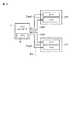
2. フラッシュメモリシステム
図1は、本発明の基本となるフラッシュメモリシステムを示している。2. Flash memory system
FIG. 1 shows a flash memory system as a basis of the present invention.
フラッシュチップCP0,CP1は、それぞれ、例えば、NANDフラッシュメモリが形成されるチップである。 The flash chips CP0 and CP1 are chips on which, for example, NAND flash memories are formed.
フラッシュチップCP0,CP1は、m+1個(mは、自然数)のブロックBK0,BK1,…BKmから構成される。ブロックBKi(i=0,1,…m)は、複数のページから構成される。 The flash chips CP0 and CP1 are composed of m + 1 (m is a natural number) blocks BK0, BK1,. The block BKi (i = 0, 1,... M) is composed of a plurality of pages.
メモリコントローラ11は、フラッシュチップCP0,CP1に対するデータ書き込み動作を制御する。 The
ここで、本例では、フラッシュチップCP0,CP1は、2個であるが、3個以上としてもよい。 In this example, the number of flash chips CP0 and CP1 is two, but may be three or more.
また、メモリコントローラ11及びフラッシュチップCP0,CP1は、1つのパッケージ内に収められていてもよいし、フラッシュチップCP0が収められるパッケージとフラッシュチップCP1が収められるパッケージとは、異なっていてもよい。 The
3. 多値フラッシュメモリ
本発明は、多値フラッシュメモリに対するデータ書き込み技術に関する。3. Multi-value flash memory
The present invention relates to a data writing technique for a multi-level flash memory.
ここで、多値とは、1つのメモリセルに3値以上のデータが記憶されることをいう。データの単位である1ビットは、2値であるため、多値フラッシュメモリは、通常、2n値(nは、自然数)を有する。1つのメモリセルにnビットが記憶されるとき、そのnビットは、下位ビット(lower bit)、中位ビット(middle bits)及び上位ビット(upper bit)で表されることとする。Here, multi-value means that data of three or more values is stored in one memory cell. Since one bit which is a unit of data is binary, a multilevel flash memory usually has2n values (n is a natural number). When n bits are stored in one memory cell, the n bits are represented by a lower bit, a middle bit, and an upper bit.
多値NANDフラッシュメモリでは、データ書き込みは、ページ単位で行われる。この場合、書き込みデータとしての下位ビットは、下位ページ(lower page)Lと呼ばれ、中位ビットは、中位ページ(middle pages)Mと呼ばれ、上位ビットは、上位ページ(upper page)Uと呼ばれる。 In the multi-level NAND flash memory, data writing is performed in units of pages. In this case, the lower bit as write data is called a lower page L, the middle bit is called a middle page M, and the upper bit is an upper page U. Called.
例えば、図2に示すように、4値NANDフラッシュメモリでは、1つのメモリセルに4値(2ビット)が記憶される。このとき、1つのメモリセルに記憶される2ビットは、下位ビット及び上位ビットで表される。 For example, as shown in FIG. 2, in a four-value NAND flash memory, four values (two bits) are stored in one memory cell. At this time, 2 bits stored in one memory cell are represented by a lower bit and an upper bit.
1つのメモリセルに下位ビットのみが記憶された状態では、メモリセルの閾値分布は、第1状態A及び第2状態Mのうちの一つになる。第1状態Aは、消去状態であり、第2状態Mは、LM(lower middle)状態と称される。 In a state where only the lower bits are stored in one memory cell, the threshold distribution of the memory cell is one of the first state A and the second state M. The first state A is an erased state, and the second state M is called an LM (lower middle) state.
1つのメモリセルに下位ビットと上位ビットとが記憶された状態では、メモリセルの閾値分布は、第1状態A、第3状態B、第4状態C及び第5状態Dのうちの一つになる。例えば、第3状態Bは、第1状態Aからの閾値シフトにより得られ、第4及び第5状態C,Dは、それぞれ、第2状態Mからの閾値シフトにより得られる。 In a state where the lower bit and the upper bit are stored in one memory cell, the threshold distribution of the memory cell is one of the first state A, the third state B, the fourth state C, and the fifth state D. Become. For example, the third state B is obtained by a threshold shift from the first state A, and the fourth and fifth states C and D are obtained by a threshold shift from the second state M, respectively.
但し、閾値のシフト方法は、これに限られることはない。 However, the threshold shift method is not limited to this.
例えば、図3に示すように、下位ビットのみが記憶された状態では、メモリセルの閾値分布を、第1状態A及び第2状態Bのうちの一つとし、下位ビットと上位ビットとが記憶された状態では、メモリセルの閾値分布を、第1状態A、第2状態B、第3状態C及び第4状態Dのうちの一つとしてもよい。 For example, as shown in FIG. 3, in the state where only the lower bits are stored, the threshold distribution of the memory cell is set to one of the first state A and the second state B, and the lower bits and the upper bits are stored. In this state, the threshold distribution of the memory cells may be one of the first state A, the second state B, the third state C, and the fourth state D.
この場合、第3状態Cは、第2状態Bからの閾値シフトにより得られ、第4状態Dは、第1状態Aからの閾値シフトにより得られる。 In this case, the third state C is obtained by a threshold shift from the second state B, and the fourth state D is obtained by a threshold shift from the first state A.
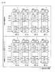
4. フラッシュメモリのブロック構成
本発明の前提となるフラッシュメモリのブロック構成について説明する。4). Flash memory block configuration
A block configuration of a flash memory which is a premise of the present invention will be described.
図4及び図5は、フラッシュメモリのブロック構成を示している。 4 and 5 show a block configuration of the flash memory.
ブロックBKi(i=0,1,…m)は、図1のブロックBK0,BK1,…BKmに相当する。 The block BKi (i = 0, 1,... M) corresponds to the blocks BK0, BK1,.
図4は、4値フラッシュメモリのブロック構成である。 FIG. 4 shows a block configuration of a quaternary flash memory.
1つのブロックBKiは、j+1個(jは、自然数)のフィジカルアドレスPA0,PA1,PA2,…PAj−1,PAjから構成される。 One block BKi is composed of j + 1 (j is a natural number) physical addresses PA0, PA1, PA2,... PAj-1, PAj.
1つのブロックBKi内の最下位のフィジカルアドレスPA0は、フィジカルページPP0の1ページのみから構成される。フィジカルページPP0は、例えば、下位ページLに設定される。 The lowest physical address PA0 in one block BKi is composed of only one page of the physical page PP0. The physical page PP0 is set to, for example, the lower page L.
また、1つのブロックBKi内の最上位のフィジカルアドレスPAjは、フィジカルページPP2j−1の1ページのみから構成される。フィジカルページPP2j−1は、例えば、上位ページUに設定される。 The highest physical address PAj in one block BKi is composed of only one page of the physical page PP2j-1. The physical page PP2j-1 is set to the upper page U, for example.
フィジカルページPP0,PP2j−1を下位ページに設定するか、又は上位ページに設定するかは、任意である。 Whether the physical pages PP0 and PP2j-1 are set to the lower page or the upper page is arbitrary.
残りのフィジカルアドレスPA1,PA2,…PAj−1は、下位ページL及び上位ページUの2ページから構成される。 The remaining physical addresses PA1, PA2,... PAj-1 are composed of two pages, a lower page L and an upper page U.
例えば、フィジカルアドレスPA1は、下位ページLとしてのフィジカルページPP1と上位ページUとしてのフィジカルページPP2とから構成される。 For example, the physical address PA1 includes a physical page PP1 as the lower page L and a physical page PP2 as the upper page U.
図5は、8値フラッシュメモリのブロック構成である。 FIG. 5 shows a block configuration of an 8-level flash memory.
1つのブロックBKiは、j+1個(jは、自然数)のフィジカルアドレスPA0,PA1,PA2,…PAj−1,PAjから構成される。 One block BKi is composed of j + 1 (j is a natural number) physical addresses PA0, PA1, PA2,... PAj-1, PAj.
1つのブロックBKi内の最下位のフィジカルアドレスPA0は、フィジカルページPP0の1ページのみから構成される。フィジカルページPP0は、例えば、下位ページLに設定される。 The lowest physical address PA0 in one block BKi is composed of only one page of the physical page PP0. The physical page PP0 is set to, for example, the lower page L.
また、1つのブロックBKi内の最上位のフィジカルアドレスPAjは、フィジカルページPP2j−1の1ページのみから構成される。フィジカルページPP2j−1は、例えば、上位ページUに設定される。 The highest physical address PAj in one block BKi is composed of only one page of the physical page PP2j-1. The physical page PP2j-1 is set to the upper page U, for example.
フィジカルページPP0,PP2j−1を下位ページに設定するか、又は上位ページに設定するかは、任意である。 Whether the physical pages PP0 and PP2j-1 are set to the lower page or the upper page is arbitrary.
残りのフィジカルアドレスPA1,PA2,…PAj−1は、下位ページL、中位ページM及び上位ページUの3ページから構成される。 The remaining physical addresses PA1, PA2,... PAj-1 are composed of three pages: a lower page L, a middle page M, and an upper page U.
例えば、フィジカルアドレスPA1は、下位ページLとしてのフィジカルページPP1と、中位ページMとしてのフィジカルページPP2と、上位ページUとしてのフィジカルページPP3とから構成される。 For example, the physical address PA1 includes a physical page PP1 as the lower page L, a physical page PP2 as the middle page M, and a physical page PP3 as the upper page U.
尚、1つのブロックBKi内の最下位のフィジカルアドレスPA0は、下位ページL及び中位ページMの2ページから構成されていてもよい。また、1つのブロックBKi内の最上位のフィジカルアドレスPAjは、中位ページM及び上位ページUの2ページから構成されていてもよい。 The lowest physical address PA0 in one block BKi may be composed of two pages, a lower page L and a middle page M. Further, the highest physical address PAj in one block BKi may be composed of two pages, the middle page M and the upper page U.
図6は、NANDフラッシュメモリのブロック構成を示している。 FIG. 6 shows a block configuration of the NAND flash memory.
ここでは、図4のブロック構成に対応させて、4値の例を説明する。 Here, an example of four values will be described in correspondence with the block configuration of FIG.
NANDセルユニットCUは、直列接続されるj+1個のメモリセルMCと、その両端に1つずつ接続される合計2つのセレクトゲートトランジスタST1,ST2とから構成される。セレクトゲートトランジスタST1は、ソース線SLに接続され、セレクトゲートトランジスタST2は、ビット線BL0に接続される。 The NAND cell unit CU is composed of j + 1 memory cells MC connected in series, and a total of two select gate transistors ST1, ST2 connected one by one to both ends thereof. Select gate transistor ST1 is connected to source line SL, and select gate transistor ST2 is connected to bit line BL0.
ワード線WL0,WL1,WL2,…WLj−1、WLjは、メモリセルMCに接続され、セレクトゲート線SGS,SGDは、セレクトゲートトランジスタST1,ST2に接続される。 Word lines WL0, WL1, WL2,... WLj−1, WLj are connected to memory cell MC, and select gate lines SGS, SGD are connected to select gate transistors ST1, ST2.
1つのブロックBKiは、j+1個のフィジカルアドレスPA0,PA1,PA2,…PAj−1,PAjから構成される。 One block BKi is composed of j + 1 physical addresses PA0, PA1, PA2,... PAj-1, PAj.
1つのブロックBKi内の最下位のフィジカルアドレスPA0は、フィジカルページ(下位ページ)PP0の1ページのみから構成される。 The lowest physical address PA0 in one block BKi is composed of only one page of the physical page (lower page) PP0.
また、1つのブロックBKi内の最上位のフィジカルアドレスPAjは、フィジカルページ(上位ページ)PP2j−1の1ページから構成される。 The highest physical address PAj in one block BKi is composed of one page of the physical page (upper page) PP2j-1.
残りのフィジカルアドレスPA1,PA2,…PAj−1は、下位ページL及び上位ページUの2ページから構成される。 The remaining physical addresses PA1, PA2,... PAj-1 are composed of two pages, a lower page L and an upper page U.
以上の説明では、4値(2ビット)と8値(3ビット)のブロック構成について説明したが、例えば、図5の中位ビットMの数を増やすことにより、容易に、16値(4ビット)、32値(5ビット)、64値(6ビット)…に応用することができる。 In the above description, the block configuration of 4 values (2 bits) and 8 values (3 bits) has been described. For example, by increasing the number of middle bits M in FIG. ), 32 values (5 bits), 64 values (6 bits)...
これらフラッシュメモリのブロック構成の特徴は、1つのブロックBKi内の最下位のフィジカルアドレスPA0のページ構成(1ページのみ)が、フィジカルアドレスPA1、PA2,…PAj−1のページ構成(複数ページ)と異なっていることにある。 The feature of these flash memory block configurations is that the page configuration (only one page) of the lowest physical address PA0 in one block BKi is different from the page configuration (multiple pages) of physical addresses PA1, PA2,. It is different.
これは、以下に説明するページシフト動作及びジグザグインターリーブ動作を実行するに当って高速書き込みを妨げる一つの要因となる。 This is one factor that hinders high-speed writing in performing the page shift operation and zigzag interleave operation described below.
5. ページシフト動作
ページシフト動作は、フラッシュメモリにおいて高速書き込みを実現するために開発された技術の一つである。5. Page shift operation
The page shift operation is one of techniques developed for realizing high-speed writing in a flash memory.
本発明は、ページシフト動作を前提とするため、以下、これについて説明する。 Since the present invention is premised on a page shift operation, this will be described below.
フラッシュメモリは、例えば、データ消去をブロック単位で行い、データ書き込みをページ単位で行う。一方、データは、ページサイズよりも小さいサイズ、例えば、セクタで管理される。 For example, the flash memory performs data erasure in units of blocks and performs data writing in units of pages. On the other hand, data is managed in a size smaller than the page size, for example, a sector.
ここで、フラッシュメモリに新規データを書き込むときは、例えば、データ消去済みの未使用ブロック(ニューブロック)に対して、セクタ単位で管理される新規データを、最下位のフィジカルページから最上位のフィジカルページに向かって、順次、ページ単位で書き込むことができる。 Here, when writing new data to the flash memory, for example, new data managed in units of sectors is transferred from the lowest physical page to the highest physical data for unused blocks (new blocks) whose data has been erased. It is possible to write in page units sequentially toward the page.
これに対し、データが書き込まれている使用中ブロック(オールドブロック)内のページの一部(例えば、セクタ)を上書きデータ(over writing data)により変更するときは、上書きの対象となるページの一部のみを変更することはできないため、例えば、新たにデータ消去済みの未使用ブロック(ニューブロック)を用意し、この未使用ブロックに上書きデータを書き込む。 On the other hand, when a part (for example, sector) of a page in an in-use block (old block) in which data is written is changed by overwriting data, one page to be overwritten is overwritten. For example, a new unused block (new block) from which data has been erased is prepared, and overwritten data is written in this unused block.
図7及び図8は、上書き動作の例を示している。
本例では、1つのブロックは、128ページから構成されるものとする。7 and 8 show examples of the overwrite operation.
In this example, one block is composed of 128 pages.
まず、未使用ブロックBK−AのフィジカルページPP0,PP1,PP2,PP3,PP4,…PP125,PP126,PP127に対して、ロジカルページLP0,LP1,LP2,LP3,LP4,…LP125,LP126,LP127の新規データをページ単位で順次書き込む。データが書き込まれたブロックBK−Aは、使用中ブロックになる。 First, for the physical pages PP0, PP1, PP2, PP3, PP4,... PP125, PP126, PP127 of the unused block BK-A, the logical pages LP0, LP1, LP2, LP3, LP4,. Write new data sequentially in page units. The block BK-A in which data is written becomes a busy block.
この後、ロジカルページLP125,LP126,LP127に対して上書きを行う場合を考える。この場合、まず、使用中ブロックBK−Aとは別の未使用ブロックBK−Bを用意する。 Thereafter, consider a case where the logical pages LP125, LP126, and LP127 are overwritten. In this case, first, an unused block BK-B different from the in-use block BK-A is prepared.
ここで、未使用ブロックBK−Bに対するデータ書き込みは、フィジカルページPP0からフィジカルページPP127に向かって、順次、ページ単位で行われる。 Here, data writing to the unused block BK-B is sequentially performed in units of pages from the physical page PP0 to the physical page PP127.
従って、図7の例では、使用中ブロックBK−A内のフィジカルページPP0〜PP124のデータ(有効データ)を未使用ブロックBK−Bにコピーした後、上書きデータとしてのロジカルページLP125〜LP127のデータを未使用ブロックBK−BのフィジカルページPP125〜PP127に書き込む。 Therefore, in the example of FIG. 7, after the data (valid data) of the physical pages PP0 to PP124 in the used block BK-A are copied to the unused block BK-B, the data of the logical pages LP125 to LP127 as overwrite data Are written to the physical pages PP125 to PP127 of the unused block BK-B.
しかし、この制御では、データを上書きする前に、常に、使用中ブロックBK−Aから未使用ブロックBK−Bへのデータのコピーを行う必要があるため、データ書き込み速度の高速化を図ることができない。 However, in this control, it is necessary to always copy data from the in-use block BK-A to the unused block BK-B before overwriting the data, so that the data writing speed can be increased. Can not.
これに対し、図8の例では、上書きデータは、常に、未使用ブロックBK−Bの最下位のフィジカルページPP0から順次書き込む。具体的には、上書きデータとしてのロジカルページLP125〜LP127のデータは、未使用ブロックBK−BのフィジカルページPP0〜PP2に書き込む。 On the other hand, in the example of FIG. 8, the overwrite data is always written sequentially from the lowest physical page PP0 of the unused block BK-B. Specifically, the data of the logical pages LP125 to LP127 as the overwrite data is written to the physical pages PP0 to PP2 of the unused block BK-B.
この制御をページシフト動作と呼ぶ。 This control is called a page shift operation.
ページシフト動作によれば、使用中ブロックBK−A内のページの一部を上書きデータにより変更するときに、使用中ブロックBK−A内のデータを未使用ブロックBK−Bにコピーしなくてよいため、データ書き込み速度の高速化を図ることができる。 According to the page shift operation, when a part of the page in the in-use block BK-A is changed by the overwrite data, the data in the in-use block BK-A does not have to be copied to the unused block BK-B. Therefore, the data writing speed can be increased.
但し、ページシフト動作では、コントローラにより、ロジカルページとフィジカルページとの関係を管理することが重要である。 However, in the page shift operation, it is important to manage the relationship between the logical page and the physical page by the controller.
そして、ブロックBK−A内の残りの有効データ、即ち、ロジカルページLP0〜LP124のデータは、適当な時期に、例えば、ブロックBK−A内のフィジカルページPP0〜PP124からブロックBK−B内のフィジカルページPP3〜PP127に移動させる。 Then, the remaining valid data in the block BK-A, that is, the data in the logical pages LP0 to LP124, is transferred from the physical pages PP0 to PP124 in the block BK-A to the physical data in the block BK-B at an appropriate time, for example. Move to pages PP3 to PP127.
ブロックBK−A内の有効データの移動後において、ブロックBK−Aは、無効データのみを有する。このため、ブロックBK−Aに対してデータ消去が行われると、ブロックBK−Aは、再び、未使用ブロックとして取り扱われる。 After the movement of valid data in the block BK-A, the block BK-A has only invalid data. For this reason, when data erasure is performed on the block BK-A, the block BK-A is again handled as an unused block.
このように、使用中ブロックが再び未使用ブロックに戻ることを撤収と呼ぶ。 In this way, returning the used block to the unused block again is called withdrawal.
6. ジグザクインターリーブ動作
ジグザグインターリーブ動作も、フラッシュメモリにおいて高速書き込みを実現するために開発された技術の一つである。6). Zigzag interleave operation
Zigzag interleave operation is also one of the technologies developed for realizing high-speed writing in flash memory.
本発明は、ジグザグインターリーブ動作を前提とするため、以下、これについて説明する。ジグザグとは、多値フラッシュメモリに対するデータ書き込みにインターリーブ動作を適用したときに、複数のチップのフィジカルページに対するデータ書き込みの順番をジグザグにすると、高速書き込みに貢献できることから付けられた名称である。 Since the present invention assumes a zigzag interleave operation, this will be described below. Zigzag is a name given because it can contribute to high-speed writing when the order of data writing to physical pages of a plurality of chips is made zigzag when an interleave operation is applied to data writing to a multi-level flash memory.
(1) ノーマルインターリーブ動作
ジグザグインターリーブ動作を理解するには、まず、ノーマルインターリーブ動作を知っておく必要があるため、これについて説明する。(1) Normal interleave operation
In order to understand the zigzag interleaving operation, it is first necessary to know the normal interleaving operation, which will be described.
図9は、ノーマルインターリーブ動作の書き込み手順を示している。
ここでは、インターリーブの対象となるチップ数は、2つとし、1つのブロックは、128ページから構成されるものとする。FIG. 9 shows a writing procedure of a normal interleave operation.
Here, the number of chips to be interleaved is two, and one block is composed of 128 pages.
初期書き込みでは、2つのフラッシュチップCP0,CP1内の未使用ブロックBK−AのフィジカルページPP0,PP1,PP2,PP3,PP4,…PP125,PP126,PP127に対して、交互に、ロジカルページLP0,LP1,LP2,LP3,LP4,…LP125,LP126,LP127の新規データをページ単位で順次書き込む。 In the initial write, the logical pages LP0, LP1 are alternately alternately provided to the physical pages PP0, PP1, PP2, PP3, PP4,..., PP125, PP126, PP127 of the unused block BK-A in the two flash chips CP0, CP1. , LP2, LP3, LP4,..., LP125, LP126, LP127 are sequentially written in page units.
例えば、まず、ロジカルページLP0のデータを、フラッシュチップCP0の未使用ブロックBK−AのフィジカルページPP0(下位ページL)に書き込む。次に、ロジカルページLP1のデータを、フラッシュチップCP1の未使用ブロックBK−AのフィジカルページPP0(下位ページL)に書き込む。 For example, first, the data of the logical page LP0 is written into the physical page PP0 (lower page L) of the unused block BK-A of the flash chip CP0. Next, the data of the logical page LP1 is written into the physical page PP0 (lower page L) of the unused block BK-A of the flash chip CP1.
続けて、ロジカルページLP2のデータを、フラッシュチップCP0の未使用ブロックBK−AのフィジカルページPP1(下位ページL)に書き込む。次に、ロジカルページLP3のデータを、フラッシュチップCP1の未使用ブロックBK−AのフィジカルページPP1(下位ページL)に書き込む。 Subsequently, the data of the logical page LP2 is written into the physical page PP1 (lower page L) of the unused block BK-A of the flash chip CP0. Next, the data of the logical page LP3 is written to the physical page PP1 (lower page L) of the unused block BK-A of the flash chip CP1.
以下、同様に、ロジカルページLP4,LP5,…LP254,LP255のデータを順次書き込む。 Thereafter, similarly, data of logical pages LP4, LP5,... LP254, LP255 are sequentially written.
データが書き込まれたブロックBK−Aは、使用中ブロックになる。 The block BK-A in which data is written becomes a busy block.
この後、ロジカルページLP4,LP5,LP6,LP7に対して上書きを行う場合を考える。この場合、まず、使用中ブロックBK−Aとは別の未使用ブロックBK−Bを用意する。 Next, consider a case where the logical pages LP4, LP5, LP6, LP7 are overwritten. In this case, first, an unused block BK-B different from the in-use block BK-A is prepared.
ここで、未使用ブロックBK−Bに対するデータ書き込みは、上述したページシフト動作により、フィジカルページPP0からフィジカルページPP127に向かって、順次、ページ単位で行うものとする。 Here, data writing to the unused block BK-B is sequentially performed in units of pages from the physical page PP0 to the physical page PP127 by the above-described page shift operation.
即ち、上書き動作では、2つのフラッシュチップCP0,CP1内の未使用ブロックBK−BのフィジカルページPP0,PP1に対して、交互に、ロジカルページLP4,LP5,LP6,LP7のデータを書き込む。 That is, in the overwrite operation, the data of the logical pages LP4, LP5, LP6, and LP7 are alternately written into the physical pages PP0 and PP1 of the unused block BK-B in the two flash chips CP0 and CP1.
具体的には、まず、ロジカルページLP4のデータを、フラッシュチップCP0の未使用ブロックBK−BのフィジカルページPP0(下位ページL)に書き込む。次に、ロジカルページLP5のデータを、フラッシュチップCP1の未使用ブロックBK−BのフィジカルページPP0(下位ページL)に書き込む。 Specifically, first, the data of the logical page LP4 is written into the physical page PP0 (lower page L) of the unused block BK-B of the flash chip CP0. Next, the data of the logical page LP5 is written into the physical page PP0 (lower page L) of the unused block BK-B of the flash chip CP1.
続けて、ロジカルページLP6のデータを、フラッシュチップCP0の未使用ブロックBK−BのフィジカルページPP1(下位ページL)に書き込む。次に、ロジカルページLP7のデータを、フラッシュチップCP1の未使用ブロックBK−BのフィジカルページPP1(下位ページL)に書き込む。 Subsequently, the data of the logical page LP6 is written into the physical page PP1 (lower page L) of the unused block BK-B of the flash chip CP0. Next, the data of the logical page LP7 is written into the physical page PP1 (lower page L) of the unused block BK-B of the flash chip CP1.
そして、ブロックBK−A内の残りの有効データ、即ち、ロジカルページLP0〜LP3,LP8〜LP255のデータは、適当な時期に、例えば、ブロックBK−A内のフィジカルページPP0,PP1,PP4〜PP127からブロックBK−B内のフィジカルページPP2〜PP127に移動させる。 Then, the remaining valid data in the block BK-A, that is, the data of the logical pages LP0 to LP3, LP8 to LP255, is, for example, the physical pages PP0, PP1, PP4 to PP127 in the block BK-A at an appropriate time. To physical pages PP2 to PP127 in the block BK-B.
図10は、ノーマルインターリーブの動作波形を示している。
ノーマルインターリーブ動作では、例えば、2つのフラッシュチップCP0,CP1に対して交互にデータを入力することにより、実質的に、2つのフラッシュチップCP0,CP1に対する書き込みを並行して行うことができ、見かけ上の書き込み速度を向上させることができる。FIG. 10 shows an operation waveform of normal interleaving.
In the normal interleave operation, for example, by alternately inputting data to the two flash chips CP0 and CP1, writing to the two flash chips CP0 and CP1 can be substantially performed in parallel. The writing speed can be improved.
しかし、上述したフラッシュメモリの特有のブロック構成により、インターリーブが有効に機能せず、書き込み速度を大幅に向上させることが難しい。 However, due to the unique block configuration of the flash memory described above, interleaving does not function effectively, and it is difficult to significantly improve the writing speed.
なぜなら、多値フラッシュメモリでは、下位ページ、中位ページ及び上位ページに対する書き込み時間がそれぞれ異なっているからである。例えば、下位ページに対する書き込み時間は、最も短く、上位ページに対する書き込み時間は、最も長い。 This is because the multi-level flash memory has different write times for the lower page, the middle page, and the upper page. For example, the write time for the lower page is the shortest and the write time for the upper page is the longest.
即ち、ノーマルインターリーブ動作では、フラッシュチップCP0に対する下位ページの書き込み中に、フラッシュチップCP1に対する下位ページの入力を行い、フラッシュチップCP1に対する下位ページの書き込み中に、フラッシュチップCP0に対する上位ページの入力を行い、フラッシュチップCP0に対する上位ページの書き込み中に、フラッシュチップCP1に対する上位ページの入力を行う。 That is, in the normal interleave operation, the lower page is input to the flash chip CP1 while the lower page is being written to the flash chip CP0, and the upper page is input to the flash chip CP0 while the lower page is being written to the flash chip CP1. While the upper page is being written to the flash chip CP0, the upper page is input to the flash chip CP1.
この場合、下位ページの書き込み時間は短いため、例えば、フラッシュチップCP0に対するロジカルページLP2の書き込み(Busy期間)中に、フラッシュチップCP1に対するロジカルページLP3のデータ入力を行うのは好ましくない。 In this case, since the write time of the lower page is short, for example, it is not preferable to input data of the logical page LP3 to the flash chip CP1 during writing of the logical page LP2 to the flash chip CP0 (Busy period).
また、上位ページの書き込み時間は長いため、例えば、フラッシュチップCP0に対するロジカルページLP4の上位ページへの書き込み(Busy期間)中に、フラッシュチップCP1に対するロジカルページLP5のデータ入力のみを行うのは効率的ではない。 Further, since the upper page write time is long, for example, it is efficient to input only the data of the logical page LP5 to the flash chip CP1 during the write (busy period) of the logical page LP4 to the flash chip CP0. is not.
この例では、ロジカルページLP4の書き込みのために生じる見かけ上のBusy期間Xが長くなるため、インターリーブによる高速書き込みの効果が制限される。 In this example, the apparent busy period X generated for writing the logical page LP4 becomes longer, so that the effect of high-speed writing by interleaving is limited.
(2) ジグザグインターリーブ動作
ジグザグインターリーブ動作は、ノーマルインターリーブ動作の問題点を解消する。その特徴は、下位ページと上位ページとをペアで書き込むことにある。(2) Zigzag interleave operation
The zigzag interleave operation eliminates the problems of normal interleave operation. The feature is that the lower page and the upper page are written in pairs.
図11は、ジグザグインターリーブ動作の書き込み手順を示している。
ここでは、インターリーブの対象となるチップ数は、2つとし、1つのブロックは、128ページから構成されるものとする。FIG. 11 shows a writing procedure of the zigzag interleave operation.
Here, the number of chips to be interleaved is two, and one block is composed of 128 pages.
初期書き込みでは、2つのフラッシュチップCP0,CP1内の未使用ブロックBK−AのフィジカルページPP0,PP1,PP2,PP3,PP4,…PP125,PP126,PP127に対して、ジグザクに、ロジカルページLP0,LP1,LP2,LP3,LP4,…LP125,LP126,LP127の新規データをページ単位で順次書き込む。 In the initial writing, the logical pages LP0 and LP1 are zigzag to the physical pages PP0, PP1, PP2, PP3, PP4,... , LP2, LP3, LP4,..., LP125, LP126, LP127 are sequentially written in page units.
例えば、まず、ロジカルページLP0のデータを、フラッシュチップCP0の未使用ブロックBK−AのフィジカルページPP0(下位ページL)に書き込む。次に、ロジカルページLP1のデータを、フラッシュチップCP1の未使用ブロックBK−AのフィジカルページPP0(下位ページL)に書き込む。 For example, first, the data of the logical page LP0 is written into the physical page PP0 (lower page L) of the unused block BK-A of the flash chip CP0. Next, the data of the logical page LP1 is written into the physical page PP0 (lower page L) of the unused block BK-A of the flash chip CP1.
続けて、ロジカルページLP2,LP3のデータを、フラッシュチップCP0の未使用ブロックBK−AのフィジカルページPP1(下位ページL),PP2(上位ページ)に書き込む。次に、ロジカルページLP4,LP5のデータを、フラッシュチップCP1の未使用ブロックBK−AのフィジカルページPP1(下位ページL),PP2(上位ページ)に書き込む。 Subsequently, the data of the logical pages LP2 and LP3 are written to the physical pages PP1 (lower page L) and PP2 (upper page) of the unused block BK-A of the flash chip CP0. Next, the data of the logical pages LP4 and LP5 are written to the physical pages PP1 (lower page L) and PP2 (upper page) of the unused block BK-A of the flash chip CP1.
以下、同様に、ロジカルページLP6,LP7,…LP254,LP255のデータを順次書き込む。 Thereafter, similarly, data of logical pages LP6, LP7,... LP254, LP255 are sequentially written.
データが書き込まれたブロックBK−Aは、使用中ブロックになる。 The block BK-A in which data is written becomes a busy block.
この後、ロジカルページLP2〜LP7に対して上書きを行う場合を考える。この場合、まず、使用中ブロックBK−Aとは別の未使用ブロックBK−Bを用意する。 Next, consider a case where the logical pages LP2 to LP7 are overwritten. In this case, first, an unused block BK-B different from the in-use block BK-A is prepared.
ここで、未使用ブロックBK−Bに対するデータ書き込みは、上述したページシフト動作により、フィジカルページPP0からフィジカルページPP127に向かって、順次、ページ単位で行うものとする。 Here, data writing to the unused block BK-B is sequentially performed in units of pages from the physical page PP0 to the physical page PP127 by the above-described page shift operation.
即ち、上書き動作では、2つのフラッシュチップCP0,CP1内の未使用ブロックBK−BのフィジカルページPP0,PP1に対して、ジグザグに、ロジカルページLP2〜LP7のデータを書き込む。 That is, in the overwrite operation, the data of the logical pages LP2 to LP7 is written in a zigzag manner to the physical pages PP0 and PP1 of the unused block BK-B in the two flash chips CP0 and CP1.
具体的には、まず、ロジカルページLP2のデータを、フラッシュチップCP0の未使用ブロックBK−BのフィジカルページPP0(下位ページL)に書き込む。次に、ロジカルページLP3のデータを、フラッシュチップCP1の未使用ブロックBK−BのフィジカルページPP0(下位ページL)に書き込む。 Specifically, first, the data of the logical page LP2 is written into the physical page PP0 (lower page L) of the unused block BK-B of the flash chip CP0. Next, the data of the logical page LP3 is written into the physical page PP0 (lower page L) of the unused block BK-B of the flash chip CP1.
続けて、ロジカルページLP4、LP5のデータを、フラッシュチップCP0の未使用ブロックBK−BのフィジカルページPP1(下位ページL),PP2(上位ページU)に書き込む。次に、ロジカルページLP6,LP7のデータを、フラッシュチップCP1の未使用ブロックBK−BのフィジカルページPP1(下位ページL),PP2(上位ページU)に書き込む。 Subsequently, the data of the logical pages LP4 and LP5 is written into the physical pages PP1 (lower page L) and PP2 (upper page U) of the unused block BK-B of the flash chip CP0. Next, the data of the logical pages LP6 and LP7 are written into the physical pages PP1 (lower page L) and PP2 (upper page U) of the unused block BK-B of the flash chip CP1.
そして、ブロックBK−A内の残りの有効データ、即ち、ロジカルページLP0,LP1,LP8〜LP255のデータは、適当な時期に、例えば、ブロックBK−A内のフィジカルページPP0,PP3〜PP127からブロックBK−B内のフィジカルページPP3〜PP127に移動させる。 Then, the remaining valid data in the block BK-A, that is, the data of the logical pages LP0, LP1, LP8 to LP255 are blocked from the physical pages PP0, PP3 to PP127 in the block BK-A at an appropriate time, for example. Move to physical pages PP3 to PP127 in BK-B.
図12は、ジグザグインターリーブの動作波形を示している。
ジグザグインターリーブ動作では、例えば、2つのフラッシュチップCP0,CP1に対してジグザグにデータを入力することにより、実質的に、2つのフラッシュチップCP0,CP1に対する書き込みを並行して行うことができ、見かけ上の書き込み速度を向上させることができる。FIG. 12 shows operation waveforms of zigzag interleaving.
In the zigzag interleave operation, for example, by writing data to the two flash chips CP0 and CP1 in a zigzag manner, the writing to the two flash chips CP0 and CP1 can be substantially performed in parallel. The writing speed can be improved.
また、書き込みは、下位ページと上位ページとをペアにして続けて行うため、常に、1つのフラッシュチップの上位ページの書き込みによって生じるBusy期間を利用して、残りの1つ又は複数のフラッシュチップに対する下位ページ及び上位ページの入力を行う。 In addition, since writing is continuously performed by pairing the lower page and the upper page, the Busy period generated by writing the upper page of one flash chip is always used for the remaining one or more flash chips. Input the lower page and upper page.
例えば、フラッシュチップCP0に対するロジカルページLP3の上位ページへの書き込み(Busy期間)中に、フラッシュチップCP1に対するロジカルページLP4,LP5のデータ入力を行う。 For example, during the writing (Busy period) of the logical page LP3 to the flash chip CP0, data is input to the logical pages LP4 and LP5 to the flash chip CP1.
従って、ロジカルページLP3の書き込みのために生じる見かけ上のBusy期間Xが短くなるため、インターリーブによる高速書き込みの効果が最大となる。 Accordingly, since the apparent busy period X generated for writing the logical page LP3 is shortened, the effect of high-speed writing by interleaving is maximized.
この最大の効果は、ジグザクインターリーブの対象となるフラッシュチップの数を、上位ページ書き込みのBusy期間に基づいて最適値に設定することで実現される。 This maximum effect is realized by setting the number of flash chips to be zigzag interleaved to an optimal value based on the busy period of upper page writing.
以上のジグザグインターリーブ動作について説明したが、その特徴は、複数のフラッシュチップに対してインターリーブ書き込みを行うに当って、下位ページと上位ページとをペアにして書き込みを行い、上位ページの書き込みによって生じるBusy期間を利用して、下位ページ及び上位ページの入力を行う、ということにある。 The zigzag interleaving operation described above has been described. The feature is that when performing interleaved writing to a plurality of flash chips, writing is performed by pairing the lower page and the upper page, and the Busy generated by writing the upper page. The lower page and the upper page are input using the period.
従って、この書き込み順序を崩さないことが重要になる。 Therefore, it is important not to break this writing order.
しかし、上述したフラッシュメモリの特有のブロック構成により、ジグザグインターリーブ動作によっても、インターリーブが有効に機能しないモードがある。 However, due to the unique block configuration of the flash memory described above, there is a mode in which interleaving does not function effectively even by a zigzag interleaving operation.
このモードは、上書き時に発生する。 This mode occurs when overwriting.
(3) ジグザグインターリーブ動作の課題
ジグザグインターリーブ動作の課題は、データの上書きをページシフト動作により行うときに発生する。(3) Issues of zigzag interleave operation
The problem of the zigzag interleave operation occurs when data is overwritten by a page shift operation.
ジグザグインターリーブ動作の特徴は、上述のように、複数のフラッシュチップに対してインターリーブ書き込みを行うに当って、下位ページと上位ページとをペアにして連続して書き込みを行うことにある。 As described above, the feature of the zigzag interleaving operation is that, when interleave writing is performed on a plurality of flash chips, the lower page and the upper page are continuously written in pairs.
従って、この書き込み順序を崩さずに、ページシフト動作により上書きデータを書き込むことが必要である。 Therefore, it is necessary to write the overwrite data by the page shift operation without breaking the order of writing.
例えば、図11の例では、ロジカルページLP2〜LP7に対して上書きを行う。 For example, in the example of FIG. 11, the logical pages LP2 to LP7 are overwritten.
ロジカルページLP2のデータは、フラッシュチップCP0の未使用ブロックBK−BのフィジカルページPP0(下位ページL)に書き込まれ、ロジカルページLP3のデータは、フラッシュチップCP1の未使用ブロックBK−BのフィジカルページPP0(下位ページL)に書き込まれる。 The data of the logical page LP2 is written to the physical page PP0 (lower page L) of the unused block BK-B of the flash chip CP0, and the data of the logical page LP3 is the physical page of the unused block BK-B of the flash chip CP1. Written in PP0 (lower page L).
また、ロジカルページLP4、LP5のデータは、フラッシュチップCP0の未使用ブロックBK−BのフィジカルページPP1(下位ページL),PP2(上位ページU)に書き込まれ、ロジカルページLP6,LP7のデータは、フラッシュチップCP1の未使用ブロックBK−BのフィジカルページPP1(下位ページL),PP2(上位ページU)に書き込まれる。 Further, the data of the logical pages LP4 and LP5 are written to the physical pages PP1 (lower page L) and PP2 (upper page U) of the unused block BK-B of the flash chip CP0, and the data of the logical pages LP6 and LP7 are Data is written to physical pages PP1 (lower page L) and PP2 (upper page U) of the unused block BK-B of the flash chip CP1.
この後、ブロックBK−A内の残りの有効データ、即ち、ロジカルページLP0,LP1,LP8〜LP255のデータを、例えば、ブロックBK−A内のフィジカルページPP0,PP3〜PP127からブロックBK−B内のフィジカルページPP3〜PP127に移動させ、ブロックBK−Aの撤収を図る。 Thereafter, the remaining valid data in the block BK-A, that is, the data of the logical pages LP0, LP1, LP8 to LP255, is transferred from the physical pages PP0, PP3 to PP127 in the block BK-A to the block BK-B, for example. The physical pages PP3 to PP127 are moved to block BK-A.
しかし、この場合、フラッシュチップCP1内のブロックBK−Aに記憶されているロジカルページLP8,LP9〜LP252,LP253,LP255のデータは、フラッシュチップCP0内のブロックBK−Bにコピーしなければならない(Copy 1)。 However, in this case, the data of the logical pages LP8, LP9 to LP252, LP253, and LP255 stored in the block BK-A in the flash chip CP1 must be copied to the block BK-B in the flash chip CP0 ( Copy 1).
また、フラッシュチップCP0内のブロックBK−Aに記憶されているロジカルページLP10,LP11〜LP250,LP251,LP254のデータは、フラッシュチップCP1内のブロックBK−Bにコピーしなければならない(Copy 2)。 Further, the data of the logical pages LP10, LP11 to LP250, LP251, and LP254 stored in the block BK-A in the flash chip CP0 must be copied to the block BK-B in the flash chip CP1 (Copy 2). .
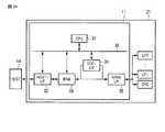
このコピーでは、データは、異なる2つのチップ間を移動することになるため、この動作を実行するに当たっては、データを一時的に記憶する外部メモリ、例えば、図13に示すように、メモリコントローラ11内のメモリMが必要になる。 In this copy, data moves between two different chips. Therefore, when executing this operation, an external memory that temporarily stores data, for example, a
従って、ジグザグインターリーブ動作とページシフト動作とにより、書き込みの高速化を図っても、データ上書き後にブロックBK−Aの撤収を行うに当たって、データの移動に多大な時間を要することになる。この撤収時間の増加により、結果として、書き込み速度の大幅な改善を図ることはできない。 Therefore, even if the writing speed is increased by the zigzag interleaving operation and the page shift operation, it takes much time to move the data when the block BK-A is withdrawn after the data is overwritten. As a result of this increase in withdrawal time, the writing speed cannot be significantly improved.
尚、この例では、ロジカルページLP0のデータは、フラッシュチップCP0内のブロックBK−AからブロックBK−Bにコピーされ(Copy 3)、ロジカルページLP255,LP1のデータは、フラッシュチップCP1内のブロックBK−AからブロックBK−Bにコピーされる(Copy 4)。 In this example, the data on the logical page LP0 is copied from the block BK-A in the flash chip CP0 to the block BK-B (Copy 3), and the data on the logical pages LP255 and LP1 is copied to the block in the flash chip CP1. The data is copied from BK-A to block BK-B (Copy 4).
ところで、フラッシュチップ(例えば、NANDフラッシュメモリ)は、データを一時的に記憶しておくことが可能なページバッファを有している。これを利用すれば、フラッシュチップ内の異なるブロック間でデータを高速移動させることができる。 Incidentally, a flash chip (for example, a NAND flash memory) has a page buffer capable of temporarily storing data. If this is utilized, data can be moved at high speed between different blocks in the flash chip.
以下に説明する実施例では、データの上書きを、ジグザグインターリーブ動作及びページシフト動作により行っても、上書き後のブロックの撤収時においては、常に、データコピーが同一のフラッシュチップ内で行われることにより、書き込み速度の大幅な改善を図ることができる技術について提案する。 In the embodiment described below, even when data is overwritten by a zigzag interleave operation and a page shift operation, data copy is always performed within the same flash chip when the block after overwriting is withdrawn. We propose a technique that can greatly improve the writing speed.
7. 実施例
本発明の例では、ロジカルページの初期書き込み時及び上書き時に、それぞれ、ロジカルページを一時的に記憶するテンポラリメモリを使用し、オールドブロックの撤収時に異なるフラッシュチップ間でデータ移動が生じることを防ぐことで、ページシフト動作及びインターリーブ動作による高速書き込みを実現する。7). Example
In the example of the present invention, temporary memory that temporarily stores a logical page is used at the time of initial writing and overwriting of a logical page, respectively, and data movement between different flash chips is prevented when an old block is withdrawn. Thus, high-speed writing is realized by a page shift operation and an interleave operation.
以下では、インターリーブ動作を、2つのフラッシュチップで行う場合と、4つのフラッシュチップで行う場合とについて説明する。 Hereinafter, a case where the interleaving operation is performed with two flash chips and a case where the interleaving operation is performed with four flash chips will be described.
(1) 第1実施例
第1実施例は、インターリーブ動作を2つのフラッシュチップで行う場合である。(1) First embodiment
The first embodiment is a case where the interleave operation is performed by two flash chips.
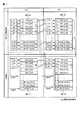
図14乃至図17は、第1実施例の書き込み手順を示している。
ここでは、1つのブロックは、128ページから構成されるものとする。14 to 17 show the write procedure of the first embodiment.
Here, one block is composed of 128 pages.
初期書き込みでは、テンポラリメモリTを使用し、フラッシュチップCP0,CP1内のニューブロックBK−Aに対するロジカルページの書き込みを、2個のロジカルページをペアとして、以下の順番で行う。 In the initial writing, the temporary memory T is used, and logical pages are written into the new block BK-A in the flash chips CP0 and CP1 in the following order with two logical pages as a pair.
テンポラリメモリTは、例えば、図18に示すように、フラッシュチップCP0,CP1内のブロックBK−(T)の最下位のフィジカルページPP0(下位ページL)とすることができる。また、本例とは関係ないが、8値(3ビット)以上のフラッシュメモリでは、テンポラリメモリTを、ブロックBK−(T)の複数のフィジカルページPP0,PP1,…とすることができる。 For example, as shown in FIG. 18, the temporary memory T can be the lowest physical page PP0 (lower page L) of the block BK- (T) in the flash chips CP0 and CP1. Although not related to this example, in a flash memory of 8 values (3 bits) or more, the temporary memory T can be a plurality of physical pages PP0, PP1,... Of the block BK- (T).
まず、第1ステップとして、フラッシュチップCP0内のテンポラリメモリT及びブロックBK−A内のフィジカルページPP0(下位ページL)に対して、2個のロジカルページLP0,LP1をペアにして連続して書き込む。 First, as a first step, two logical pages LP0 and LP1 are successively written in pairs to the temporary memory T in the flash chip CP0 and the physical page PP0 (lower page L) in the block BK-A. .
次に、第2ステップとして、フラッシュチップCP1内のテンポラリメモリT及びブロックBK−A内のフィジカルページPP0(下位ページL)に対して、2個のロジカルページLP2,LP3をペアにして連続して書き込む。 Next, as a second step, two logical pages LP2 and LP3 are successively paired with the temporary memory T in the flash chip CP1 and the physical page PP0 (lower page L) in the block BK-A. Write.
ここで、上述の第1及び第2ステップでは、それぞれ、ロジカルページの書き込み順序が下位ページ→上位ページでないが、テンポラリメモリTをフラッシュチップCP0内のブロックBK−(T)の最下位のフィジカルページPP0(下位ページL)とすれば、高速書き込みが大きく制限されることはない。 Here, in the first and second steps described above, the logical page write order is not the lower page → the upper page, but the temporary memory T is stored in the lowest physical page of the block BK- (T) in the flash chip CP0. With PP0 (lower page L), high-speed writing is not greatly limited.
次に、第3ステップとして、フラッシュチップCP0内のブロックBK−A内のフィジカルページPP1(下位ページL)及びフィジカルページPP2(上位ページU)に対して、2個のロジカルページLP4,LP5をペアにして連続して書き込む。 Next, as a third step, two logical pages LP4 and LP5 are paired with respect to the physical page PP1 (lower page L) and physical page PP2 (upper page U) in the block BK-A in the flash chip CP0. Write continuously.
次に、第4ステップとして、フラッシュチップCP1内のブロックBK−A内のフィジカルページPP1(下位ページL)及びフィジカルページPP2(上位ページU)に対して、2個のロジカルページLP6,LP7をペアにして連続して書き込む。 Next, as a fourth step, two logical pages LP6 and LP7 are paired with respect to the physical page PP1 (lower page L) and physical page PP2 (upper page U) in the block BK-A in the flash chip CP1. Write continuously.
ここで、上述の第3及び第4ステップでは、それぞれ、ロジカルページの書き込み順序が下位ページ→上位ページであるため、フラッシュチップCP0,CP1の一方に対する上位ページの書き込み時に生じるBusy期間を利用して、フラッシュチップCP0,CP1の他方に対する下位ページ及び上位ページの入力を行い、インターリーブ動作による高速書き込みを実現できる。 Here, in the above-described third and fourth steps, since the logical page writing order is from the lower page to the upper page, the busy period generated when the upper page is written to one of the flash chips CP0 and CP1 is used. By inputting the lower page and the upper page to the other of the flash chips CP0 and CP1, high-speed writing by an interleave operation can be realized.
以下、第3及び第4ステップと同様にして、ロジカルページLP8,LP9,LP10,LP11…LP252,LP253,LP254,LP255を順次書き込む。 Thereafter, logical pages LP8, LP9, LP10, LP11... LP252, LP253, LP254, and LP255 are sequentially written in the same manner as in the third and fourth steps.
最後に、第5ステップとして、フラッシュチップCP0内のテンポラリメモリTに書き込まれたロジカルページLP0を、フラッシュチップCP0内のブロックBK−Aの最上位のフィジカルページPP127(上位ページU)にコピーし、フラッシュチップCP1内のテンポラリメモリTに書き込まれたロジカルページLP2を、フラッシュチップCP1内のブロックBK−Aの最上位のフィジカルページPP127(上位ページU)にコピーする。 Finally, as a fifth step, the logical page LP0 written in the temporary memory T in the flash chip CP0 is copied to the uppermost physical page PP127 (upper page U) of the block BK-A in the flash chip CP0. The logical page LP2 written in the temporary memory T in the flash chip CP1 is copied to the uppermost physical page PP127 (upper page U) of the block BK-A in the flash chip CP1.
ロジカルデータLP0〜LP255が書き込まれたフラッシュチップCP0,CP1内のブロックBK−Aは、使用中ブロック(オールドブロック)になる。 The block BK-A in the flash chips CP0 and CP1 in which the logical data LP0 to LP255 are written becomes an in-use block (old block).
この後、上書きを行う場合を考える。 Next, consider the case of overwriting.
・ フラッシュチップCP0内の偶数ロジカルページ(LP)からの上書き
この上書きの書き込み手順は、図14に示すようになる。
上書きは、ロジカルページLP4〜LP7に対して行うものとする。-Overwrite from even logical page (LP) in flash chip CP0
The overwriting procedure is as shown in FIG.
The overwriting is performed on the logical pages LP4 to LP7.
上書きでも、テンポラリメモリTを使用し、フラッシュチップCP0,CP1内のニューブロックBK−Bに対するロジカルページの書き込みを、2個のロジカルページをペアとして、以下の順番で行う。 Even in overwriting, the temporary memory T is used, and the logical pages are written to the new blocks BK-B in the flash chips CP0 and CP1 in the following order with two logical pages as a pair.
まず、第1ステップとして、フラッシュチップCP0内のテンポラリメモリT及びブロックBK−B内のフィジカルページPP0(下位ページL)に対して、上書きデータとしての2個のロジカルページLP4,LP5をペアにして連続して書き込む。 First, as a first step, a pair of two logical pages LP4 and LP5 as overwrite data is paired with the temporary memory T in the flash chip CP0 and the physical page PP0 (lower page L) in the block BK-B. Write continuously.
次に、第2ステップとして、フラッシュチップCP1内のテンポラリメモリT及びブロックBK−B内のフィジカルページPP0(下位ページL)に対して、上書きデータとしての2個のロジカルページLP6,LP7をペアにして連続して書き込む。 Next, as a second step, two logical pages LP6 and LP7 as overwritten data are paired with the temporary memory T in the flash chip CP1 and the physical page PP0 (lower page L) in the block BK-B. Write continuously.
ここで、上述の第1及び第2ステップでは、それぞれ、ロジカルページの書き込み順序が下位ページ→上位ページでないが、テンポラリメモリTをフラッシュチップCP0,CP1内のブロックBK−(T)の最下位のフィジカルページPP0(下位ページL)とすれば、高速書き込みが大きく制限されることはない。 Here, in the first and second steps described above, the logical page writing order is not the lower page → the upper page, but the temporary memory T is stored in the lowest order of the blocks BK- (T) in the flash chips CP0 and CP1. If the physical page PP0 (lower page L) is used, high-speed writing is not greatly limited.
この後、フラッシュチップCP0,CP1内のオールドブロックBK−AからニューブロックBK−Bへ、ロジカルページLP8,LP9〜LP254,LP255及びロジカルページLP0,LP1,LP2,LP3を、それぞれ移動させ(Copy 1, Copy 2)、オールドブロックBK−Aの撤収を図る。 Thereafter, the logical pages LP8, LP9 to LP254, LP255 and the logical pages LP0, LP1, LP2, LP3 are moved from the old block BK-A in the flash chips CP0, CP1 to the new block BK-B, respectively (Copy 1). , Copy 2), withdrawing the old block BK-A.
まず、第3ステップとして、フラッシュチップCP0内のブロックBK−B内のフィジカルページPP1(下位ページL)及びフィジカルページPP2(上位ページU)に対して、フラッシュチップCP0内のブロックBK−A内のフィジカルページPP3(下位ページL)及びフィジカルページPP4(上位ページU)の2個のロジカルページLP8,LP9をペアにして連続して書き込む。 First, as a third step, for the physical page PP1 (lower page L) and physical page PP2 (upper page U) in the block BK-B in the flash chip CP0, in the block BK-A in the flash chip CP0. Two logical pages LP8 and LP9 of the physical page PP3 (lower page L) and the physical page PP4 (upper page U) are sequentially written as a pair.
次に、第4ステップとして、フラッシュチップCP1内のブロックBK−B内のフィジカルページPP1(下位ページL)及びフィジカルページPP2(上位ページU)に対して、フラッシュチップCP1内のブロックBK−A内のフィジカルページPP3(下位ページL)及びフィジカルページPP4(上位ページU)の2個のロジカルページLP10,LP11をペアにして連続して書き込む。 Next, as a fourth step, in the block BK-A in the flash chip CP1 with respect to the physical page PP1 (lower page L) and physical page PP2 (upper page U) in the block BK-B in the flash chip CP1. The two logical pages LP10 and LP11 of the physical page PP3 (lower page L) and the physical page PP4 (upper page U) are sequentially written in pairs.
ここで、上述の第3及び第4ステップでは、それぞれ、ロジカルページの書き込み順序が下位ページ→上位ページであるため、フラッシュチップCP0,CP1の一方に対する上位ページの書き込み時に生じるBusy期間を利用して、フラッシュチップCP0,CP1の他方に対する下位ページ及び上位ページの入力を行い、インターリーブ動作による高速書き込みを実現できる。 Here, in the above-described third and fourth steps, since the logical page writing order is from the lower page to the upper page, the busy period generated when the upper page is written to one of the flash chips CP0 and CP1 is used. By inputting the lower page and the upper page to the other of the flash chips CP0 and CP1, high-speed writing by an interleave operation can be realized.
また、この第3及び第4ステップでのデータ移動は、常に、同一のフラッシュチップ内のみで行われるため、フラッシュチップに搭載されたブロック間でのデータの高速移動機能を利用し、撤収時間の短縮による高速書き込みを実現できる。 In addition, since the data movement in the third and fourth steps is always performed only within the same flash chip, the high-speed data movement function between the blocks mounted on the flash chip is used to reduce the withdrawal time. High speed writing can be realized by shortening.
以下、第3及び第4ステップと同様にして、ロジカルページLP12,LP13,LP14,LP15…LP252,LP253,LP254,LP255及びロジカルページLP0,LP1,LP2,LP3を順次書き込む。 Thereafter, logical pages LP12, LP13, LP14, LP15... LP252, LP253, LP254, LP255 and logical pages LP0, LP1, LP2, LP3 are sequentially written in the same manner as in the third and fourth steps.
最後に、第5ステップとして、フラッシュチップCP0内のテンポラリメモリTに書き込まれたロジカルページLP4を、フラッシュチップCP0内のブロックBK−Bの最上位のフィジカルページPP127(上位ページU)にコピーし、フラッシュチップCP1内のテンポラリメモリTに書き込まれたロジカルページLP6を、フラッシュチップCP1内のブロックBK−Bの最上位のフィジカルページPP127(上位ページU)にコピーする。 Finally, as a fifth step, the logical page LP4 written in the temporary memory T in the flash chip CP0 is copied to the uppermost physical page PP127 (upper page U) of the block BK-B in the flash chip CP0. The logical page LP6 written in the temporary memory T in the flash chip CP1 is copied to the uppermost physical page PP127 (upper page U) of the block BK-B in the flash chip CP1.
ロジカルデータLP0〜LP255が書き込まれたフラッシュチップCP0,CP1内のブロックBK−Bは、使用中ブロック(オールドブロック)になる。 The blocks BK-B in the flash chips CP0 and CP1 in which the logical data LP0 to LP255 are written become in-use blocks (old blocks).
以上のような書き込み手順によれば、ページシフト動作によるロジカルページの上書きを、いずれのロジカルページから繰り返し行っても、同一のフラッシュチップ内でのロジカルページの順番を崩すことがない。言い換えれば、ロジカルページの順番は、ブロックが変わる度に、同一のフラッシュチップ内でシフトするだけである。 According to the write procedure as described above, the logical page order in the same flash chip is not lost even if the logical page is overwritten by the page shift operation from any logical page. In other words, the logical page order only shifts within the same flash chip each time the block changes.
従って、オールドブロックの撤収を行うとき、ロジカルページのデータは、同一のフラッシュチップ内での移動のみとなるため、フラッシュチップに搭載されたブロック間でのデータの高速移動機能を利用し、撤収時間の短縮による高速書き込みを実現できる。 Therefore, when the old block is withdrawn, the logical page data can only be moved within the same flash chip, so use the high-speed data movement function between the blocks mounted on the flash chip, and the withdrawal time. High-speed writing can be realized by shortening.
・ フラッシュチップCP1内の偶数ロジカルページ(LP)からの上書き
この上書きの書き込み手順は、図15に示すようになる。
上書きは、ロジカルページLP2〜LP5に対して行うものとする。-Overwrite from even logical page (LP) in flash chip CP1
The overwriting procedure is as shown in FIG.
The overwriting is performed on the logical pages LP2 to LP5.
上書きでも、テンポラリメモリTを使用し、フラッシュチップCP0,CP1内のニューブロックBK−Bに対するロジカルページの書き込みを、2個のロジカルページをペアとして、以下の順番で行う。 Even in overwriting, the temporary memory T is used, and the logical pages are written to the new blocks BK-B in the flash chips CP0 and CP1 in the following order with two logical pages as a pair.
まず、第1ステップとして、フラッシュチップCP1内のテンポラリメモリT及びブロックBK−B内のフィジカルページPP0(下位ページL)に対して、上書きデータとしての2個のロジカルページLP2,LP3をペアにして連続して書き込む。 First, as a first step, two logical pages LP2 and LP3 as overwrite data are paired with the temporary memory T in the flash chip CP1 and the physical page PP0 (lower page L) in the block BK-B. Write continuously.
次に、第2ステップとして、フラッシュチップCP0内のテンポラリメモリT及びブロックBK−B内のフィジカルページPP0(下位ページL)に対して、上書きデータとしての2個のロジカルページLP4,LP5をペアにして連続して書き込む。 Next, as a second step, two logical pages LP4 and LP5 as overwrite data are paired with the temporary memory T in the flash chip CP0 and the physical page PP0 (lower page L) in the block BK-B. Write continuously.
ここで、上述の第1及び第2ステップでは、それぞれ、ロジカルページの書き込み順序が下位ページ→上位ページでないが、テンポラリメモリTをフラッシュチップCP0,CP1内のブロックBK−(T)の最下位のフィジカルページPP0(下位ページL)とすれば、高速書き込みが大きく制限されることはない。 Here, in the first and second steps described above, the logical page writing order is not the lower page → the upper page, but the temporary memory T is stored in the lowest order of the blocks BK- (T) in the flash chips CP0 and CP1. If the physical page PP0 (lower page L) is used, high-speed writing is not greatly limited.
この後、フラッシュチップCP0,CP1内のオールドブロックBK−AからニューブロックBK−Bへ、ロジカルページLP6,LP7〜LP254,LP255及びロジカルページLP0,LP1を、それぞれ移動させ(Copy 1, Copy 2)、オールドブロックBK−Aの撤収を図る。 Thereafter, the logical pages LP6, LP7 to LP254, LP255 and the logical pages LP0, LP1 are respectively moved from the old block BK-A in the flash chips CP0, CP1 to the new block BK-B (
まず、第3ステップとして、フラッシュチップCP1内のブロックBK−B内のフィジカルページPP1(下位ページL)及びフィジカルページPP2(上位ページU)に対して、フラッシュチップCP1内のブロックBK−A内のフィジカルページPP1(下位ページL)及びフィジカルページPP2(上位ページU)の2個のロジカルページLP6,LP7をペアにして連続して書き込む。 First, as a third step, the physical page PP1 (lower page L) and the physical page PP2 (upper page U) in the block BK-B in the flash chip CP1 are stored in the block BK-A in the flash chip CP1. Two logical pages LP6 and LP7 of the physical page PP1 (lower page L) and the physical page PP2 (upper page U) are sequentially written as a pair.
次に、第4ステップとして、フラッシュチップCP0内のブロックBK−B内のフィジカルページPP1(下位ページL)及びフィジカルページPP2(上位ページU)に対して、フラッシュチップCP0内のブロックBK−A内のフィジカルページPP3(下位ページL)及びフィジカルページPP4(上位ページU)の2個のロジカルページLP8,LP9をペアにして連続して書き込む。 Next, as a fourth step, in the block BK-A in the flash chip CP0 with respect to the physical page PP1 (lower page L) and physical page PP2 (upper page U) in the block BK-B in the flash chip CP0. The two logical pages LP8 and LP9 of the physical page PP3 (lower page L) and the physical page PP4 (upper page U) are sequentially written in pairs.
ここで、上述の第3及び第4ステップでは、それぞれ、ロジカルページの書き込み順序が下位ページ→上位ページであるため、フラッシュチップCP0,CP1の一方に対する上位ページの書き込み時に生じるBusy期間を利用して、フラッシュチップCP0,CP1の他方に対する下位ページ及び上位ページの入力を行い、インターリーブ動作による高速書き込みを実現できる。 Here, in the above-described third and fourth steps, since the logical page writing order is from the lower page to the upper page, the busy period generated when the upper page is written to one of the flash chips CP0 and CP1 is used. By inputting the lower page and the upper page to the other of the flash chips CP0 and CP1, high-speed writing by an interleave operation can be realized.
また、この第3及び第4ステップでのデータ移動は、常に、同一のフラッシュチップ内のみで行われるため、フラッシュチップに搭載されたブロック間でのデータの高速移動機能を利用し、撤収時間の短縮による高速書き込みを実現できる。 In addition, since the data movement in the third and fourth steps is always performed only within the same flash chip, the high-speed data movement function between the blocks mounted on the flash chip is used to reduce the withdrawal time. High-speed writing can be realized by shortening.
以下、第3及び第4ステップと同様にして、ロジカルページLP10,LP11,LP12,LP13…LP252,LP253,LP254,LP255及びロジカルページLP0,LP1を順次書き込む。 Thereafter, logical pages LP10, LP11, LP12, LP13... LP252, LP253, LP254, LP255 and logical pages LP0, LP1 are sequentially written in the same manner as in the third and fourth steps.
最後に、第5ステップとして、フラッシュチップCP1内のテンポラリメモリTに書き込まれたロジカルページLP2を、フラッシュチップCP1内のブロックBK−Bの最上位のフィジカルページPP127(上位ページU)にコピーし、フラッシュチップCP0内のテンポラリメモリTに書き込まれたロジカルページLP4を、フラッシュチップCP0内のブロックBK−Bの最上位のフィジカルページPP127(上位ページU)にコピーする。 Finally, as a fifth step, the logical page LP2 written in the temporary memory T in the flash chip CP1 is copied to the uppermost physical page PP127 (upper page U) of the block BK-B in the flash chip CP1, The logical page LP4 written in the temporary memory T in the flash chip CP0 is copied to the uppermost physical page PP127 (upper page U) of the block BK-B in the flash chip CP0.
ロジカルデータLP0〜LP255が書き込まれたフラッシュチップCP0,CP1内のブロックBK−Bは、使用中ブロック(オールドブロック)になる。 The blocks BK-B in the flash chips CP0 and CP1 in which the logical data LP0 to LP255 are written become in-use blocks (old blocks).
以上のような書き込み手順によれば、ページシフト動作によるロジカルページの上書きを、いずれのロジカルページから繰り返し行っても、同一のフラッシュチップ内でのロジカルページの順番を崩すことがない。言い換えれば、ロジカルページの順番は、ブロックが変わる度に、同一のフラッシュチップ内でシフトするだけである。 According to the write procedure as described above, the logical page order in the same flash chip is not lost even if the logical page is overwritten by the page shift operation from any logical page. In other words, the logical page order only shifts within the same flash chip each time the block changes.
従って、オールドブロックの撤収を行うとき、ロジカルページのデータは、同一のフラッシュチップ内での移動のみとなるため、フラッシュチップに搭載されたブロック間でのデータの高速移動機能を利用し、撤収時間の短縮による高速書き込みを実現できる。 Therefore, when the old block is withdrawn, the logical page data can only be moved within the same flash chip, so use the high-speed data movement function between the blocks mounted on the flash chip, and the withdrawal time. High-speed writing can be realized by shortening.
・ フラッシュチップCP0内の奇数ロジカルページ(LP)からの上書き
この上書きの書き込み手順は、図16に示すようになる。
上書きは、ロジカルページLP5〜LP7に対して行うものとする。-Overwrite from odd logical page (LP) in flash chip CP0
The overwriting procedure is as shown in FIG.
The overwriting is performed on the logical pages LP5 to LP7.
この上書きでは、フラッシュチップCP1内のテンポラリメモリTのみを使用し、フラッシュチップCP0,CP1内のニューブロックBK−Bに対するロジカルページの書き込みを、2個のロジカルページをペアとして、以下の順番で行う。 In this overwriting, only the temporary memory T in the flash chip CP1 is used, and logical pages are written in the new blocks BK-B in the flash chips CP0 and CP1 in the following order with two logical pages as a pair. .
まず、第1ステップとして、フラッシュチップCP0内のブロックBK−B内のフィジカルページPP0(下位ページL)に対して、上書きデータとしてのロジカルページLP5を書き込む。 First, as a first step, a logical page LP5 as overwritten data is written into the physical page PP0 (lower page L) in the block BK-B in the flash chip CP0.
次に、第2ステップとして、フラッシュチップCP1内のテンポラリメモリT及びブロックBK−B内のフィジカルページPP0(下位ページL)に対して、上書きデータとしての2個のロジカルページLP6,LP7をペアにして連続して書き込む。 Next, as a second step, two logical pages LP6 and LP7 as overwritten data are paired with the temporary memory T in the flash chip CP1 and the physical page PP0 (lower page L) in the block BK-B. Write continuously.
ここで、上述の第2ステップでは、ロジカルページの書き込み順序が下位ページ→上位ページでないが、テンポラリメモリTをフラッシュチップCP1内のブロックBK−(T)の最下位のフィジカルページPP0(下位ページL)とすれば、高速書き込みが大きく制限されることはない。 Here, in the above-described second step, the logical page writing order is not the lower page → the upper page, but the temporary memory T is stored in the lowest physical page PP0 (lower page L) of the block BK- (T) in the flash chip CP1. ), High-speed writing is not greatly limited.
この後、フラッシュチップCP0,CP1内のオールドブロックBK−AからニューブロックBK−Bへ、ロジカルページLP8,LP9〜LP254,LP255及びロジカルページLP0,LP1,LP2,LP3,LP4を、それぞれ移動させ(Copy 1, Copy 2)、オールドブロックBK−Aの撤収を図る。 Thereafter, the logical pages LP8, LP9 to LP254, LP255 and the logical pages LP0, LP1, LP2, LP3, LP4 are moved from the old block BK-A in the flash chips CP0, CP1 to the new block BK-B, respectively (
まず、第3ステップとして、フラッシュチップCP0内のブロックBK−B内のフィジカルページPP1(下位ページL)及びフィジカルページPP2(上位ページU)に対して、フラッシュチップCP0内のブロックBK−A内のフィジカルページPP3(下位ページL)及びフィジカルページPP4(上位ページU)の2個のロジカルページLP8,LP9をペアにして連続して書き込む。 First, as a third step, for the physical page PP1 (lower page L) and physical page PP2 (upper page U) in the block BK-B in the flash chip CP0, in the block BK-A in the flash chip CP0. Two logical pages LP8 and LP9 of the physical page PP3 (lower page L) and the physical page PP4 (upper page U) are sequentially written as a pair.
次に、第4ステップとして、フラッシュチップCP1内のブロックBK−B内のフィジカルページPP1(下位ページL)及びフィジカルページPP2(上位ページU)に対して、フラッシュチップCP1内のブロックBK−A内のフィジカルページPP3(下位ページL)及びフィジカルページPP4(上位ページU)の2個のロジカルページLP10,LP11をペアにして連続して書き込む。 Next, as a fourth step, in the block BK-A in the flash chip CP1 with respect to the physical page PP1 (lower page L) and physical page PP2 (upper page U) in the block BK-B in the flash chip CP1. The two logical pages LP10 and LP11 of the physical page PP3 (lower page L) and the physical page PP4 (upper page U) are sequentially written in pairs.
ここで、上述の第3及び第4ステップでは、それぞれ、ロジカルページの書き込み順序が下位ページ→上位ページであるため、フラッシュチップCP0,CP1の一方に対する上位ページの書き込み時に生じるBusy期間を利用して、フラッシュチップCP0,CP1の他方に対する下位ページ及び上位ページの入力を行い、インターリーブ動作による高速書き込みを実現できる。 Here, in the above-described third and fourth steps, since the logical page writing order is from the lower page to the upper page, the busy period generated when the upper page is written to one of the flash chips CP0 and CP1 is used. By inputting the lower page and the upper page to the other of the flash chips CP0 and CP1, high-speed writing by an interleave operation can be realized.
また、この第3及び第4ステップでのデータ移動は、常に、同一のフラッシュチップ内のみで行われるため、フラッシュチップに搭載されたブロック間でのデータの高速移動機能を利用し、撤収時間の短縮による高速書き込みを実現できる。 In addition, since the data movement in the third and fourth steps is always performed only within the same flash chip, the high-speed data movement function between the blocks mounted on the flash chip is used to reduce the withdrawal time. High-speed writing can be realized by shortening.
以下、第3及び第4ステップと同様にして、ロジカルページLP12,LP13,LP14,LP15…LP252,LP253,LP254,LP255及びロジカルページLP0,LP1,LP2,LP3,LP4を順次書き込む。 Thereafter, logical pages LP12, LP13, LP14, LP15... LP252, LP253, LP254, LP255 and logical pages LP0, LP1, LP2, LP3, LP4 are sequentially written in the same manner as in the third and fourth steps.
最後に、第5ステップとして、フラッシュチップCP1内のテンポラリメモリTに書き込まれたロジカルページLP6を、フラッシュチップCP1内のブロックBK−Bの最上位のフィジカルページPP127(上位ページU)にコピーする。 Finally, as a fifth step, the logical page LP6 written in the temporary memory T in the flash chip CP1 is copied to the uppermost physical page PP127 (upper page U) of the block BK-B in the flash chip CP1.
ロジカルデータLP0〜LP255が書き込まれたフラッシュチップCP0,CP1内のブロックBK−Bは、使用中ブロック(オールドブロック)になる。 The blocks BK-B in the flash chips CP0 and CP1 in which the logical data LP0 to LP255 are written become in-use blocks (old blocks).
以上のような書き込み手順によれば、ページシフト動作によるロジカルページの上書きを、いずれのロジカルページから繰り返し行っても、同一のフラッシュチップ内でのロジカルページの順番を崩すことがない。言い換えれば、ロジカルページの順番は、ブロックが変わる度に、同一のフラッシュチップ内でシフトするだけである。 According to the write procedure as described above, the logical page order in the same flash chip is not lost even if the logical page is overwritten by the page shift operation from any logical page. In other words, the logical page order only shifts within the same flash chip each time the block changes.
従って、オールドブロックの撤収を行うとき、ロジカルページのデータは、同一のフラッシュチップ内での移動のみとなるため、フラッシュチップに搭載されたブロック間でのデータの高速移動機能を利用し、撤収時間の短縮による高速書き込みを実現できる。 Therefore, when the old block is withdrawn, the logical page data can only be moved within the same flash chip, so use the high-speed data movement function between the blocks mounted on the flash chip, and the withdrawal time. High-speed writing can be realized by shortening.
・ フラッシュチップCP1内の奇数ロジカルページ(LP)からの上書き
この上書きの書き込み手順は、図17に示すようになる。
上書きは、ロジカルページLP3〜LP5に対して行うものとする。-Overwrite from odd logical page (LP) in flash chip CP1
The overwriting procedure is as shown in FIG.
The overwriting is performed on the logical pages LP3 to LP5.
この上書きでは、フラッシュチップCP0内のテンポラリメモリTのみを使用し、フラッシュチップCP0,CP1内のニューブロックBK−Bに対するロジカルページの書き込みを、2個のロジカルページをペアとして、以下の順番で行う。 In this overwriting, only the temporary memory T in the flash chip CP0 is used, and logical pages are written in the new blocks BK-B in the flash chips CP0 and CP1 in the following order with two logical pages as a pair. .
まず、第1ステップとして、フラッシュチップCP1内のブロックBK−B内のフィジカルページPP0(下位ページL)に対して、上書きデータとしてのロジカルページLP3を書き込む。 First, as a first step, a logical page LP3 as overwritten data is written into the physical page PP0 (lower page L) in the block BK-B in the flash chip CP1.
次に、第2ステップとして、フラッシュチップCP0内のテンポラリメモリT及びブロックBK−B内のフィジカルページPP0(下位ページL)に対して、上書きデータとしての2個のロジカルページLP4,LP5をペアにして連続して書き込む。 Next, as a second step, two logical pages LP4 and LP5 as overwrite data are paired with the temporary memory T in the flash chip CP0 and the physical page PP0 (lower page L) in the block BK-B. Write continuously.
ここで、上述の第2ステップでは、ロジカルページの書き込み順序が下位ページ→上位ページでないが、テンポラリメモリTをフラッシュチップCP0内のブロックBK−(T)の最下位のフィジカルページPP0(下位ページL)とすれば、高速書き込みが大きく制限されることはない。 Here, in the above-described second step, the logical page writing order is not lower page → upper page, but the temporary memory T is stored in the lowest physical page PP0 (lower page L) of the block BK- (T) in the flash chip CP0. ), High-speed writing is not greatly limited.
この後、フラッシュチップCP0,CP1内のオールドブロックBK−AからニューブロックBK−Bへ、ロジカルページLP6,LP7〜LP254,LP255及びロジカルページLP0,LP1,LP2を、それぞれ移動させ(Copy 1, Copy 2)、オールドブロックBK−Aの撤収を図る。 Thereafter, the logical pages LP6, LP7 to LP254, LP255 and the logical pages LP0, LP1, LP2 are moved from the old block BK-A in the flash chips CP0, CP1 to the new block BK-B, respectively (
まず、第3ステップとして、フラッシュチップCP1内のブロックBK−B内のフィジカルページPP1(下位ページL)及びフィジカルページPP2(上位ページU)に対して、フラッシュチップCP1内のブロックBK−A内のフィジカルページPP1(下位ページL)及びフィジカルページPP2(上位ページU)の2個のロジカルページLP6,LP7をペアにして連続して書き込む。 First, as a third step, the physical page PP1 (lower page L) and the physical page PP2 (upper page U) in the block BK-B in the flash chip CP1 are stored in the block BK-A in the flash chip CP1. Two logical pages LP6 and LP7 of the physical page PP1 (lower page L) and the physical page PP2 (upper page U) are sequentially written as a pair.
次に、第4ステップとして、フラッシュチップCP0内のブロックBK−B内のフィジカルページPP1(下位ページL)及びフィジカルページPP2(上位ページU)に対して、フラッシュチップCP0内のブロックBK−A内のフィジカルページPP3(下位ページL)及びフィジカルページPP4(上位ページU)の2個のロジカルページLP8,LP9をペアにして連続して書き込む。 Next, as a fourth step, in the block BK-A in the flash chip CP0 with respect to the physical page PP1 (lower page L) and physical page PP2 (upper page U) in the block BK-B in the flash chip CP0. The two logical pages LP8 and LP9 of the physical page PP3 (lower page L) and the physical page PP4 (upper page U) are sequentially written in pairs.
ここで、上述の第3及び第4ステップでは、それぞれ、ロジカルページの書き込み順序が下位ページ→上位ページであるため、フラッシュチップCP0,CP1の一方に対する上位ページの書き込み時に生じるBusy期間を利用して、フラッシュチップCP0,CP1の他方に対する下位ページ及び上位ページの入力を行い、インターリーブ動作による高速書き込みを実現できる。 Here, in the above-described third and fourth steps, since the logical page writing order is from the lower page to the upper page, the busy period generated when the upper page is written to one of the flash chips CP0 and CP1 is used. By inputting the lower page and the upper page to the other of the flash chips CP0 and CP1, high-speed writing by an interleave operation can be realized.
また、この第3及び第4ステップでのデータ移動は、常に、同一のフラッシュチップ内のみで行われるため、フラッシュチップに搭載されたブロック間でのデータの高速移動機能を利用し、撤収時間の短縮による高速書き込みを実現できる。 In addition, since the data movement in the third and fourth steps is always performed only within the same flash chip, the high-speed data movement function between the blocks mounted on the flash chip is used to reduce the withdrawal time. High-speed writing can be realized by shortening.
以下、第3及び第4ステップと同様にして、ロジカルページLP10,LP11,LP12,LP13…LP252,LP253,LP254,LP255及びロジカルページLP0,LP1,LP2を順次書き込む。 Thereafter, logical pages LP10, LP11, LP12, LP13... LP252, LP253, LP254, LP255 and logical pages LP0, LP1, LP2 are sequentially written in the same manner as in the third and fourth steps.
最後に、第5ステップとして、フラッシュチップCP0内のテンポラリメモリTに書き込まれたロジカルページLP4を、フラッシュチップCP0内のブロックBK−Bの最上位のフィジカルページPP127(上位ページU)にコピーする。 Finally, as a fifth step, the logical page LP4 written in the temporary memory T in the flash chip CP0 is copied to the uppermost physical page PP127 (upper page U) of the block BK-B in the flash chip CP0.
ロジカルデータLP0〜LP255が書き込まれたフラッシュチップCP0,CP1内のブロックBK−Bは、使用中ブロック(オールドブロック)になる。 The blocks BK-B in the flash chips CP0 and CP1 in which the logical data LP0 to LP255 are written become in-use blocks (old blocks).
以上のような書き込み手順によれば、ページシフト動作によるロジカルページの上書きを、いずれのロジカルページから繰り返し行っても、同一のフラッシュチップ内でのロジカルページの順番を崩すことがない。言い換えれば、ロジカルページの順番は、ブロックが変わる度に、同一のフラッシュチップ内でシフトするだけである。 According to the write procedure as described above, the logical page order in the same flash chip is not lost even if the logical page is overwritten by the page shift operation from any logical page. In other words, the logical page order only shifts within the same flash chip each time the block changes.
従って、オールドブロックの撤収を行うとき、ロジカルページのデータは、同一のフラッシュチップ内での移動のみとなるため、フラッシュチップに搭載されたブロック間でのデータの高速移動機能を利用し、撤収時間の短縮による高速書き込みを実現できる。 Therefore, when the old block is withdrawn, the logical page data can only be moved within the same flash chip, so use the high-speed data movement function between the blocks mounted on the flash chip, and the withdrawal time. High-speed writing can be realized by shortening.
(2) 第2実施例
第2実施例は、インターリーブ動作を4つのフラッシュチップで行う場合である。(2) Second embodiment
The second embodiment is a case where the interleave operation is performed with four flash chips.
図19乃至図22は、第2実施例の書き込み手順を示している。
ここでは、1つのブロックは、128ページから構成されるものとする。19 to 22 show the writing procedure of the second embodiment.
Here, one block is composed of 128 pages.
初期書き込みでは、テンポラリメモリTを使用し、フラッシュチップCP0,CP1,CP2,CP3内のニューブロックBK−Aに対するロジカルページの書き込みを、2個のロジカルページをペアとして、以下の順番で行う。 In the initial writing, the temporary memory T is used, and logical pages are written to the new block BK-A in the flash chips CP0, CP1, CP2, and CP3 in the following order with two logical pages as a pair.
テンポラリメモリTは、例えば、図18に示すように、フラッシュチップCP0,CP1,CP2,CP3内のブロックBK−(T)の最下位のフィジカルページPP0(下位ページL)である。 For example, as shown in FIG. 18, the temporary memory T is the lowest physical page PP0 (lower page L) of the block BK- (T) in the flash chips CP0, CP1, CP2, and CP3.
まず、第1ステップとして、フラッシュチップCP0内のテンポラリメモリT及びブロックBK−A内のフィジカルページPP0(下位ページL)に対して、2個のロジカルページLP0,LP1をペアにして連続して書き込む。 First, as a first step, two logical pages LP0 and LP1 are successively written in pairs to the temporary memory T in the flash chip CP0 and the physical page PP0 (lower page L) in the block BK-A. .
次に、第2ステップとして、フラッシュチップCP1内のテンポラリメモリT及びブロックBK−A内のフィジカルページPP0(下位ページL)に対して、2個のロジカルページLP2,LP3をペアにして連続して書き込む。 Next, as a second step, two logical pages LP2 and LP3 are successively paired with the temporary memory T in the flash chip CP1 and the physical page PP0 (lower page L) in the block BK-A. Write.
次に、第3ステップとして、フラッシュチップCP2内のテンポラリメモリT及びブロックBK−A内のフィジカルページPP0(下位ページL)に対して、2個のロジカルページLP4,LP5をペアにして連続して書き込む。 Next, as a third step, two logical pages LP4 and LP5 are successively paired with the temporary memory T in the flash chip CP2 and the physical page PP0 (lower page L) in the block BK-A. Write.
次に、第4ステップとして、フラッシュチップCP3内のテンポラリメモリT及びブロックBK−A内のフィジカルページPP0(下位ページL)に対して、2個のロジカルページLP6,LP7をペアにして連続して書き込む。 Next, as a fourth step, two logical pages LP6 and LP7 are continuously paired with the temporary memory T in the flash chip CP3 and the physical page PP0 (lower page L) in the block BK-A. Write.
次に、第5ステップとして、フラッシュチップCP0内のブロックBK−A内のフィジカルページPP1(下位ページL)及びフィジカルページPP2(上位ページU)に対して、2個のロジカルページLP8,LP9をペアにして連続して書き込む。 Next, as a fifth step, two logical pages LP8 and LP9 are paired with respect to the physical page PP1 (lower page L) and physical page PP2 (upper page U) in the block BK-A in the flash chip CP0. Write continuously.
次に、第6ステップとして、フラッシュチップCP1内のブロックBK−A内のフィジカルページPP1(下位ページL)及びフィジカルページPP2(上位ページU)に対して、2個のロジカルページLP10,LP11をペアにして連続して書き込む。 Next, as a sixth step, two logical pages LP10 and LP11 are paired with respect to the physical page PP1 (lower page L) and physical page PP2 (upper page U) in the block BK-A in the flash chip CP1. Write continuously.
次に、第7ステップとして、フラッシュチップCP2内のブロックBK−A内のフィジカルページPP1(下位ページL)及びフィジカルページPP2(上位ページU)に対して、2個のロジカルページLP12,LP13をペアにして連続して書き込む。 Next, as a seventh step, two logical pages LP12 and LP13 are paired with respect to the physical page PP1 (lower page L) and physical page PP2 (upper page U) in the block BK-A in the flash chip CP2. Write continuously.
次に、第8ステップとして、フラッシュチップCP3内のブロックBK−A内のフィジカルページPP1(下位ページL)及びフィジカルページPP2(上位ページU)に対して、2個のロジカルページLP14,LP15をペアにして連続して書き込む。 Next, as an eighth step, two logical pages LP14 and LP15 are paired with respect to the physical page PP1 (lower page L) and physical page PP2 (upper page U) in the block BK-A in the flash chip CP3. Write continuously.
以下、第5乃至第8ステップと同様にして、ロジカルページLP16,LP17…LPLP510,LP511を順次書き込む。 Thereafter, logical pages LP16, LP17... LPLP510, LP511 are sequentially written in the same manner as in the fifth to eighth steps.
最後に、第9ステップとして、フラッシュチップCP0内のテンポラリメモリTに書き込まれたロジカルページLP0を、フラッシュチップCP0内のブロックBK−Aの最上位のフィジカルページPP127(上位ページU)にコピーし、フラッシュチップCP1内のテンポラリメモリTに書き込まれたロジカルページLP2を、フラッシュチップCP1内のブロックBK−Aの最上位のフィジカルページPP127(上位ページU)にコピーする。 Finally, as a ninth step, the logical page LP0 written in the temporary memory T in the flash chip CP0 is copied to the uppermost physical page PP127 (upper page U) of the block BK-A in the flash chip CP0. The logical page LP2 written in the temporary memory T in the flash chip CP1 is copied to the uppermost physical page PP127 (upper page U) of the block BK-A in the flash chip CP1.
また、フラッシュチップCP2内のテンポラリメモリTに書き込まれたロジカルページLP4を、フラッシュチップCP2内のブロックBK−Aの最上位のフィジカルページPP127(上位ページU)にコピーし、フラッシュチップCP3内のテンポラリメモリTに書き込まれたロジカルページLP6を、フラッシュチップCP3内のブロックBK−Aの最上位のフィジカルページPP127(上位ページU)にコピーする。 Further, the logical page LP4 written in the temporary memory T in the flash chip CP2 is copied to the uppermost physical page PP127 (upper page U) of the block BK-A in the flash chip CP2, and the temporary page in the flash chip CP3. The logical page LP6 written in the memory T is copied to the uppermost physical page PP127 (upper page U) of the block BK-A in the flash chip CP3.
ロジカルデータLP0〜LP511が書き込まれたフラッシュチップCP0,CP1,CP2,CP3内のブロックBK−Aは、使用中ブロック(オールドブロック)になる。 The block BK-A in the flash chips CP0, CP1, CP2 and CP3 in which the logical data LP0 to LP511 are written becomes an in-use block (old block).
この後、上書きを行う場合を考える。 Next, consider the case of overwriting.
・ フラッシュチップCP0内の偶数ロジカルページ(LP)からの上書き
この上書きの書き込み手順は、図19に示すようになる。
上書きは、ロジカルページLP8〜LP15に対して行うものとする。-Overwrite from even logical page (LP) in flash chip CP0
The overwriting procedure is as shown in FIG.
The overwriting is performed on the logical pages LP8 to LP15.
上書きでも、テンポラリメモリTを使用し、フラッシュチップCP0,CP1,CP2,CP3内のニューブロックBK−Bに対するロジカルページの書き込みを、2個のロジカルページをペアとして、以下の順番で行う。 Even when overwriting, the temporary memory T is used, and logical pages are written to the new block BK-B in the flash chips CP0, CP1, CP2, and CP3 in the following order with two logical pages as a pair.
まず、第1ステップとして、フラッシュチップCP0内のテンポラリメモリT及びブロックBK−B内のフィジカルページPP0(下位ページL)に対して、上書きデータとしての2個のロジカルページLP8,LP9をペアにして連続して書き込む。 First, as a first step, a pair of two logical pages LP8 and LP9 as overwrite data is paired with the temporary memory T in the flash chip CP0 and the physical page PP0 (lower page L) in the block BK-B. Write continuously.
次に、第2ステップとして、フラッシュチップCP1内のテンポラリメモリT及びブロックBK−B内のフィジカルページPP0(下位ページL)に対して、上書きデータとしての2個のロジカルページLP10,LP11をペアにして連続して書き込む。 Next, as a second step, two logical pages LP10 and LP11 as overwrite data are paired with the temporary memory T in the flash chip CP1 and the physical page PP0 (lower page L) in the block BK-B. Write continuously.
次に、第3ステップとして、フラッシュチップCP2内のテンポラリメモリT及びブロックBK−B内のフィジカルページPP0(下位ページL)に対して、上書きデータとしての2個のロジカルページLP12,LP13をペアにして連続して書き込む。 Next, as a third step, two logical pages LP12 and LP13 as overwrite data are paired with the temporary memory T in the flash chip CP2 and the physical page PP0 (lower page L) in the block BK-B. Write continuously.
次に、第4ステップとして、フラッシュチップCP3内のテンポラリメモリT及びブロックBK−B内のフィジカルページPP0(下位ページL)に対して、上書きデータとしての2個のロジカルページLP14,LP15をペアにして連続して書き込む。 Next, as a fourth step, two logical pages LP14 and LP15 as overwrite data are paired with the temporary memory T in the flash chip CP3 and the physical page PP0 (lower page L) in the block BK-B. Write continuously.
この後、フラッシュチップCP0,CP1,CP2,CP3内のオールドブロックBK−AからニューブロックBK−Bへ、ロジカルページLP16,LP17〜LP510,LP511及びロジカルページLP0,LP1〜LP6,LP7を、それぞれ移動させ、オールドブロックBK−Aの撤収を図る。 Thereafter, the logical pages LP16, LP17 to LP510, LP511 and the logical pages LP0, LP1 to LP6, LP7 are moved from the old block BK-A in the flash chips CP0, CP1, CP2, CP3 to the new block BK-B, respectively. And withdraw the old block BK-A.
まず、第5ステップとして、フラッシュチップCP0内のブロックBK−B内のフィジカルページPP1(下位ページL)及びフィジカルページPP2(上位ページU)に対して、フラッシュチップCP0内のブロックBK−A内のフィジカルページPP3(下位ページL)及びフィジカルページPP4(上位ページU)の2個のロジカルページLP16,LP17をペアにして連続して書き込む。 First, as a fifth step, for the physical page PP1 (lower page L) and physical page PP2 (upper page U) in the block BK-B in the flash chip CP0, in the block BK-A in the flash chip CP0. Two logical pages LP16 and LP17 of the physical page PP3 (lower page L) and the physical page PP4 (upper page U) are sequentially written as a pair.
次に、第6ステップとして、フラッシュチップCP1内のブロックBK−B内のフィジカルページPP1(下位ページL)及びフィジカルページPP2(上位ページU)に対して、フラッシュチップCP1内のブロックBK−A内のフィジカルページPP3(下位ページL)及びフィジカルページPP4(上位ページU)の2個のロジカルページLP18,LP19をペアにして連続して書き込む。 Next, as a sixth step, in the block BK-A in the flash chip CP1 with respect to the physical page PP1 (lower page L) and physical page PP2 (upper page U) in the block BK-B in the flash chip CP1. The two logical pages LP18 and LP19 of the physical page PP3 (lower page L) and the physical page PP4 (upper page U) are sequentially written in pairs.
次に、第7ステップとして、フラッシュチップCP2内のブロックBK−B内のフィジカルページPP1(下位ページL)及びフィジカルページPP2(上位ページU)に対して、フラッシュチップCP2内のブロックBK−A内のフィジカルページPP3(下位ページL)及びフィジカルページPP4(上位ページU)の2個のロジカルページLP20,LP21をペアにして連続して書き込む。 Next, as a seventh step, in the block BK-A in the flash chip CP2 with respect to the physical page PP1 (lower page L) and physical page PP2 (upper page U) in the block BK-B in the flash chip CP2. The two logical pages LP20 and LP21 of the physical page PP3 (lower page L) and the physical page PP4 (upper page U) are sequentially written in pairs.
次に、第8ステップとして、フラッシュチップCP3内のブロックBK−B内のフィジカルページPP1(下位ページL)及びフィジカルページPP2(上位ページU)に対して、フラッシュチップCP3内のブロックBK−A内のフィジカルページPP3(下位ページL)及びフィジカルページPP4(上位ページU)の2個のロジカルページLP22,LP23をペアにして連続して書き込む。 Next, as an eighth step, for the physical page PP1 (lower page L) and physical page PP2 (upper page U) in the block BK-B in the flash chip CP3, in the block BK-A in the flash chip CP3. The two logical pages LP22 and LP23 of the physical page PP3 (lower page L) and the physical page PP4 (upper page U) are sequentially written in pairs.
以下、第5乃至第8ステップと同様にして、ロジカルページLP24,LP25…LP510,LP511及びロジカルページLP0,LP1〜LP6,LP7を順次書き込む。 Thereafter, logical pages LP24, LP25... LP510, LP511 and logical pages LP0, LP1 to LP6, LP7 are sequentially written in the same manner as in the fifth to eighth steps.
最後に、第9ステップとして、フラッシュチップCP0内のテンポラリメモリTに書き込まれたロジカルページLP8を、フラッシュチップCP0内のブロックBK−Bの最上位のフィジカルページPP127(上位ページU)にコピーし、フラッシュチップCP1内のテンポラリメモリTに書き込まれたロジカルページLP10を、フラッシュチップCP1内のブロックBK−Bの最上位のフィジカルページPP127(上位ページU)にコピーする。 Finally, as a ninth step, the logical page LP8 written in the temporary memory T in the flash chip CP0 is copied to the uppermost physical page PP127 (upper page U) of the block BK-B in the flash chip CP0. The logical page LP10 written in the temporary memory T in the flash chip CP1 is copied to the uppermost physical page PP127 (upper page U) of the block BK-B in the flash chip CP1.
また、フラッシュチップCP2内のテンポラリメモリTに書き込まれたロジカルページLP12を、フラッシュチップCP2内のブロックBK−Bの最上位のフィジカルページPP127(上位ページU)にコピーし、フラッシュチップCP3内のテンポラリメモリTに書き込まれたロジカルページLP14を、フラッシュチップCP3内のブロックBK−Bの最上位のフィジカルページPP127(上位ページU)にコピーする。 Further, the logical page LP12 written in the temporary memory T in the flash chip CP2 is copied to the uppermost physical page PP127 (upper page U) of the block BK-B in the flash chip CP2, and the temporary page in the flash chip CP3. The logical page LP14 written in the memory T is copied to the uppermost physical page PP127 (upper page U) of the block BK-B in the flash chip CP3.
ロジカルデータLP0〜LP511が書き込まれたフラッシュチップCP0,CP1,CP2,CP3内のブロックBK−Bは、使用中ブロック(オールドブロック)になる。 The block BK-B in the flash chips CP0, CP1, CP2, and CP3 in which the logical data LP0 to LP511 are written becomes an in-use block (old block).
以上のような書き込み手順によれば、ページシフト動作によるロジカルページの上書きを、いずれのロジカルページから繰り返し行っても、同一のフラッシュチップ内でのロジカルページの順番を崩すことがない。言い換えれば、ロジカルページの順番は、ブロックが変わる度に、同一のフラッシュチップ内でシフトするだけである。 According to the write procedure as described above, the logical page order in the same flash chip is not lost even if the logical page is overwritten by the page shift operation from any logical page. In other words, the logical page order only shifts within the same flash chip each time the block changes.
従って、オールドブロックの撤収を行うとき、ロジカルページのデータは、同一のフラッシュチップ内での移動のみとなるため、フラッシュチップに搭載されたブロック間でのデータの高速移動機能を利用し、撤収時間の短縮による高速書き込みを実現できる。 Therefore, when the old block is withdrawn, the logical page data can only be moved within the same flash chip, so use the high-speed data movement function between the blocks mounted on the flash chip, and the withdrawal time. High-speed writing can be realized by shortening.
・ フラッシュチップCP2内の偶数ロジカルページ(LP)からの上書き
この上書きの書き込み手順は、図20に示すようになる。
上書きは、ロジカルページLP12〜LP19に対して行うものとする。-Overwrite from even logical page (LP) in flash chip CP2
The overwriting procedure is as shown in FIG.
The overwriting is performed on the logical pages LP12 to LP19.
上書きでも、テンポラリメモリTを使用し、フラッシュチップCP0,CP1,CP3,CP4内のニューブロックBK−Bに対するロジカルページの書き込みを、2個のロジカルページをペアとして、以下の順番で行う。 Even when overwriting, the temporary memory T is used, and logical pages are written into the new block BK-B in the flash chips CP0, CP1, CP3, and CP4 in the following order with two logical pages as a pair.
まず、第1ステップとして、フラッシュチップCP2内のテンポラリメモリT及びブロックBK−B内のフィジカルページPP0(下位ページL)に対して、上書きデータとしての2個のロジカルページLP12,LP13をペアにして連続して書き込む。 First, as a first step, a pair of two logical pages LP12 and LP13 as overwrite data is paired with the temporary memory T in the flash chip CP2 and the physical page PP0 (lower page L) in the block BK-B. Write continuously.
次に、第2ステップとして、フラッシュチップCP3内のテンポラリメモリT及びブロックBK−B内のフィジカルページPP0(下位ページL)に対して、上書きデータとしての2個のロジカルページLP14,LP15をペアにして連続して書き込む。 Next, as a second step, two logical pages LP14 and LP15 as overwrite data are paired with the temporary memory T in the flash chip CP3 and the physical page PP0 (lower page L) in the block BK-B. Write continuously.
次に、第3ステップとして、フラッシュチップCP0内のテンポラリメモリT及びブロックBK−B内のフィジカルページPP0(下位ページL)に対して、上書きデータとしての2個のロジカルページLP16,LP17をペアにして連続して書き込む。 Next, as a third step, two logical pages LP16 and LP17 as overwritten data are paired with the temporary memory T in the flash chip CP0 and the physical page PP0 (lower page L) in the block BK-B. Write continuously.
次に、第4ステップとして、フラッシュチップCP1内のテンポラリメモリT及びブロックBK−B内のフィジカルページPP0(下位ページL)に対して、上書きデータとしての2個のロジカルページLP18,LP19をペアにして連続して書き込む。 Next, as a fourth step, two logical pages LP18 and LP19 as overwrite data are paired with the temporary memory T in the flash chip CP1 and the physical page PP0 (lower page L) in the block BK-B. Write continuously.
この後、フラッシュチップCP0,CP1,CP2,CP3内のオールドブロックBK−AからニューブロックBK−Bへ、ロジカルページLP20,LP21〜LP510,LP511及びロジカルページLP0,LP1〜LP10,LP11を、それぞれ移動させ、オールドブロックBK−Aの撤収を図る。 Thereafter, the logical pages LP20, LP21 to LP510, LP511 and the logical pages LP0, LP1 to LP10, LP11 are moved from the old block BK-A in the flash chips CP0, CP1, CP2, CP3 to the new block BK-B, respectively. And withdraw the old block BK-A.
まず、第5ステップとして、フラッシュチップCP2内のブロックBK−B内のフィジカルページPP1(下位ページL)及びフィジカルページPP2(上位ページU)に対して、フラッシュチップCP2内のブロックBK−A内のフィジカルページPP3(下位ページL)及びフィジカルページPP4(上位ページU)の2個のロジカルページLP20,LP21をペアにして連続して書き込む。 First, as a fifth step, for the physical page PP1 (lower page L) and physical page PP2 (upper page U) in the block BK-B in the flash chip CP2, the contents in the block BK-A in the flash chip CP2 are changed. Two logical pages LP20 and LP21 of the physical page PP3 (lower page L) and the physical page PP4 (upper page U) are sequentially written as a pair.
次に、第6ステップとして、フラッシュチップCP3内のブロックBK−B内のフィジカルページPP1(下位ページL)及びフィジカルページPP2(上位ページU)に対して、フラッシュチップCP3内のブロックBK−A内のフィジカルページPP3(下位ページL)及びフィジカルページPP4(上位ページU)の2個のロジカルページLP22,LP23をペアにして連続して書き込む。 Next, as a sixth step, for the physical page PP1 (lower page L) and physical page PP2 (upper page U) in the block BK-B in the flash chip CP3, in the block BK-A in the flash chip CP3. The two logical pages LP22 and LP23 of the physical page PP3 (lower page L) and the physical page PP4 (upper page U) are sequentially written in pairs.
次に、第7ステップとして、フラッシュチップCP0内のブロックBK−B内のフィジカルページPP1(下位ページL)及びフィジカルページPP2(上位ページU)に対して、フラッシュチップCP0内のブロックBK−A内のフィジカルページPP5(下位ページL)及びフィジカルページPP6(上位ページU)の2個のロジカルページLP24,LP25をペアにして連続して書き込む。 Next, as a seventh step, in the block BK-A in the flash chip CP0 with respect to the physical page PP1 (lower page L) and physical page PP2 (upper page U) in the block BK-B in the flash chip CP0. The two logical pages LP24 and LP25 of the physical page PP5 (lower page L) and physical page PP6 (upper page U) are sequentially written in pairs.
次に、第8ステップとして、フラッシュチップCP1内のブロックBK−B内のフィジカルページPP1(下位ページL)及びフィジカルページPP2(上位ページU)に対して、フラッシュチップCP1内のブロックBK−A内のフィジカルページPP5(下位ページL)及びフィジカルページPP6(上位ページU)の2個のロジカルページLP26,LP27をペアにして連続して書き込む。 Next, as an eighth step, for the physical page PP1 (lower page L) and physical page PP2 (upper page U) in the block BK-B in the flash chip CP1, in the block BK-A in the flash chip CP1. The two logical pages LP26 and LP27 of the physical page PP5 (lower page L) and the physical page PP6 (upper page U) are sequentially written in pairs.
以下、第5乃至第8ステップと同様にして、ロジカルページLP28,LP29…LPLP510,LP511及びロジカルページLP0,LP1〜LP10、LP11を順次書き込む。 Thereafter, logical pages LP28, LP29... LPLP510, LP511 and logical pages LP0, LP1 to LP10, LP11 are sequentially written in the same manner as in the fifth to eighth steps.
最後に、第9ステップとして、フラッシュチップCP2内のテンポラリメモリTに書き込まれたロジカルページLP12を、フラッシュチップCP2内のブロックBK−Bの最上位のフィジカルページPP127(上位ページU)にコピーし、フラッシュチップCP3内のテンポラリメモリTに書き込まれたロジカルページLP14を、フラッシュチップCP3内のブロックBK−Bの最上位のフィジカルページPP127(上位ページU)にコピーする。 Finally, as a ninth step, the logical page LP12 written in the temporary memory T in the flash chip CP2 is copied to the uppermost physical page PP127 (upper page U) of the block BK-B in the flash chip CP2. The logical page LP14 written in the temporary memory T in the flash chip CP3 is copied to the uppermost physical page PP127 (upper page U) of the block BK-B in the flash chip CP3.
また、フラッシュチップCP0内のテンポラリメモリTに書き込まれたロジカルページLP16を、フラッシュチップCP0内のブロックBK−Bの最上位のフィジカルページPP127(上位ページU)にコピーし、フラッシュチップCP1内のテンポラリメモリTに書き込まれたロジカルページLP18を、フラッシュチップCP1内のブロックBK−Bの最上位のフィジカルページPP127(上位ページU)にコピーする。 Further, the logical page LP16 written in the temporary memory T in the flash chip CP0 is copied to the top physical page PP127 (upper page U) of the block BK-B in the flash chip CP0, and the temporary page in the flash chip CP1. The logical page LP18 written in the memory T is copied to the uppermost physical page PP127 (upper page U) of the block BK-B in the flash chip CP1.
ロジカルデータLP0〜LP511が書き込まれたフラッシュチップCP0,CP1,CP2,CP3内のブロックBK−Bは、使用中ブロック(オールドブロック)になる。 The block BK-B in the flash chips CP0, CP1, CP2, and CP3 in which the logical data LP0 to LP511 are written becomes an in-use block (old block).
以上のような書き込み手順によれば、ページシフト動作によるロジカルページの上書きを、いずれのロジカルページから繰り返し行っても、同一のフラッシュチップ内でのロジカルページの順番を崩すことがない。言い換えれば、ロジカルページの順番は、ブロックが変わる度に、同一のフラッシュチップ内でシフトするだけである。 According to the write procedure as described above, the logical page order in the same flash chip is not lost even if the logical page is overwritten by the page shift operation from any logical page. In other words, the logical page order only shifts within the same flash chip each time the block changes.
従って、オールドブロックの撤収を行うとき、ロジカルページのデータは、同一のフラッシュチップ内での移動のみとなるため、フラッシュチップに搭載されたブロック間でのデータの高速移動機能を利用し、撤収時間の短縮による高速書き込みを実現できる。 Therefore, when the old block is withdrawn, the logical page data can only be moved within the same flash chip, so use the high-speed data movement function between the blocks mounted on the flash chip, and the withdrawal time. High-speed writing can be realized by shortening.
・ フラッシュチップCP0内の奇数ロジカルページ(LP)からの上書き
この上書きの書き込み手順は、図21に示すようになる。
上書きは、ロジカルページLP9〜LP15に対して行うものとする。-Overwrite from odd logical page (LP) in flash chip CP0
The overwriting procedure is as shown in FIG.
The overwriting is performed on the logical pages LP9 to LP15.
この上書きでは、フラッシュチップCP1,CP2,CP3内のテンポラリメモリTを使用し、フラッシュチップCP0,CP1,CP2,CP3内のニューブロックBK−Bに対するロジカルページの書き込みを、2個のロジカルページをペアとして、以下の順番で行う。 In this overwriting, the temporary memory T in the flash chips CP1, CP2, CP3 is used, and the logical page write to the new block BK-B in the flash chips CP0, CP1, CP2, CP3 is performed by pairing two logical pages. As follows.
まず、第1ステップとして、フラッシュチップCP0内のブロックBK−B内のフィジカルページPP0(下位ページL)に対して、上書きデータとしてのロジカルページLP9を書き込む。 First, as a first step, a logical page LP9 as overwritten data is written into the physical page PP0 (lower page L) in the block BK-B in the flash chip CP0.
次に、第2ステップとして、フラッシュチップCP1内のテンポラリメモリT及びブロックBK−B内のフィジカルページPP0(下位ページL)に対して、上書きデータとしての2個のロジカルページLP10,LP11をペアにして連続して書き込む。 Next, as a second step, two logical pages LP10 and LP11 as overwrite data are paired with the temporary memory T in the flash chip CP1 and the physical page PP0 (lower page L) in the block BK-B. Write continuously.
次に、第3ステップとして、フラッシュチップCP2内のテンポラリメモリT及びブロックBK−B内のフィジカルページPP0(下位ページL)に対して、上書きデータとしての2個のロジカルページLP12,LP13をペアにして連続して書き込む。 Next, as a third step, two logical pages LP12 and LP13 as overwrite data are paired with the temporary memory T in the flash chip CP2 and the physical page PP0 (lower page L) in the block BK-B. Write continuously.
次に、第4ステップとして、フラッシュチップCP3内のテンポラリメモリT及びブロックBK−B内のフィジカルページPP0(下位ページL)に対して、上書きデータとしての2個のロジカルページLP14,LP15をペアにして連続して書き込む。 Next, as a fourth step, two logical pages LP14 and LP15 as overwrite data are paired with the temporary memory T in the flash chip CP3 and the physical page PP0 (lower page L) in the block BK-B. Write continuously.
この後、フラッシュチップCP0,CP1,CP2,CP3内のオールドブロックBK−AからニューブロックBK−Bへ、ロジカルページLP16,LP17〜LP510,LP511及びロジカルページLP0,LP1〜LP6,LP7を、それぞれ移動させ、オールドブロックBK−Aの撤収を図る。 Thereafter, the logical pages LP16, LP17 to LP510, LP511 and the logical pages LP0, LP1 to LP6, LP7 are moved from the old block BK-A in the flash chips CP0, CP1, CP2, CP3 to the new block BK-B, respectively. And withdraw the old block BK-A.
まず、第5ステップとして、フラッシュチップCP0内のブロックBK−B内のフィジカルページPP1(下位ページL)及びフィジカルページPP2(上位ページU)に対して、フラッシュチップCP0内のブロックBK−A内のフィジカルページPP3(下位ページL)及びフィジカルページPP4(上位ページU)の2個のロジカルページLP16,LP17をペアにして連続して書き込む。 First, as a fifth step, for the physical page PP1 (lower page L) and physical page PP2 (upper page U) in the block BK-B in the flash chip CP0, in the block BK-A in the flash chip CP0. Two logical pages LP16 and LP17 of the physical page PP3 (lower page L) and the physical page PP4 (upper page U) are sequentially written as a pair.
次に、第6ステップとして、フラッシュチップCP1内のブロックBK−B内のフィジカルページPP1(下位ページL)及びフィジカルページPP2(上位ページU)に対して、フラッシュチップCP1内のブロックBK−A内のフィジカルページPP3(下位ページL)及びフィジカルページPP4(上位ページU)の2個のロジカルページLP18,LP19をペアにして連続して書き込む。 Next, as a sixth step, in the block BK-A in the flash chip CP1 with respect to the physical page PP1 (lower page L) and physical page PP2 (upper page U) in the block BK-B in the flash chip CP1. The two logical pages LP18 and LP19 of the physical page PP3 (lower page L) and the physical page PP4 (upper page U) are sequentially written in pairs.
次に、第7ステップとして、フラッシュチップCP2内のブロックBK−B内のフィジカルページPP1(下位ページL)及びフィジカルページPP2(上位ページU)に対して、フラッシュチップCP2内のブロックBK−A内のフィジカルページPP3(下位ページL)及びフィジカルページPP4(上位ページU)の2個のロジカルページLP20,LP21をペアにして連続して書き込む。 Next, as a seventh step, in the block BK-A in the flash chip CP2 with respect to the physical page PP1 (lower page L) and physical page PP2 (upper page U) in the block BK-B in the flash chip CP2. The two logical pages LP20 and LP21 of the physical page PP3 (lower page L) and the physical page PP4 (upper page U) are sequentially written in pairs.
次に、第8ステップとして、フラッシュチップCP3内のブロックBK−B内のフィジカルページPP1(下位ページL)及びフィジカルページPP2(上位ページU)に対して、フラッシュチップCP3内のブロックBK−A内のフィジカルページPP3(下位ページL)及びフィジカルページPP4(上位ページU)の2個のロジカルページLP22,LP23をペアにして連続して書き込む。 Next, as an eighth step, for the physical page PP1 (lower page L) and physical page PP2 (upper page U) in the block BK-B in the flash chip CP3, in the block BK-A in the flash chip CP3. The two logical pages LP22 and LP23 of the physical page PP3 (lower page L) and the physical page PP4 (upper page U) are sequentially written in pairs.
以下、第5乃至第8ステップと同様にして、ロジカルページLP24,LP25…LP510,LP511及びロジカルページLP0,LP1〜LP6,LP7,LP8を順次書き込む。 Thereafter, logical pages LP24, LP25... LP510, LP511 and logical pages LP0, LP1 to LP6, LP7, LP8 are sequentially written in the same manner as in the fifth to eighth steps.
最後に、第9ステップとして、フラッシュチップCP1内のテンポラリメモリTに書き込まれたロジカルページLP10を、フラッシュチップCP1内のブロックBK−Bの最上位のフィジカルページPP127(上位ページU)にコピーする。 Finally, as a ninth step, the logical page LP10 written in the temporary memory T in the flash chip CP1 is copied to the uppermost physical page PP127 (upper page U) of the block BK-B in the flash chip CP1.
また、フラッシュチップCP2内のテンポラリメモリTに書き込まれたロジカルページLP12を、フラッシュチップCP2内のブロックBK−Bの最上位のフィジカルページPP127(上位ページU)にコピーし、フラッシュチップCP3内のテンポラリメモリTに書き込まれたロジカルページLP14を、フラッシュチップCP3内のブロックBK−Bの最上位のフィジカルページPP127(上位ページU)にコピーする。 Further, the logical page LP12 written in the temporary memory T in the flash chip CP2 is copied to the uppermost physical page PP127 (upper page U) of the block BK-B in the flash chip CP2, and the temporary page in the flash chip CP3. The logical page LP14 written in the memory T is copied to the uppermost physical page PP127 (upper page U) of the block BK-B in the flash chip CP3.
ロジカルデータLP0〜LP511が書き込まれたフラッシュチップCP0,CP1,CP2,CP3内のブロックBK−Bは、使用中ブロック(オールドブロック)になる。 The block BK-B in the flash chips CP0, CP1, CP2, and CP3 in which the logical data LP0 to LP511 are written becomes an in-use block (old block).
以上のような書き込み手順によれば、ページシフト動作によるロジカルページの上書きを、いずれのロジカルページから繰り返し行っても、同一のフラッシュチップ内でのロジカルページの順番を崩すことがない。言い換えれば、ロジカルページの順番は、ブロックが変わる度に、同一のフラッシュチップ内でシフトするだけである。 According to the write procedure as described above, the logical page order in the same flash chip is not lost even if the logical page is overwritten by the page shift operation from any logical page. In other words, the logical page order only shifts within the same flash chip each time the block changes.
従って、オールドブロックの撤収を行うとき、ロジカルページのデータは、同一のフラッシュチップ内での移動のみとなるため、フラッシュチップに搭載されたブロック間でのデータの高速移動機能を利用し、撤収時間の短縮による高速書き込みを実現できる。 Therefore, when the old block is withdrawn, the logical page data can only be moved within the same flash chip, so use the high-speed data movement function between the blocks mounted on the flash chip, and the withdrawal time. High-speed writing can be realized by shortening.
・ フラッシュチップCP2内の奇数ロジカルページ(LP)からの上書き
この上書きの書き込み手順は、図22に示すようになる。
上書きは、ロジカルページLP13〜LP19に対して行うものとする。-Overwrite from odd logical page (LP) in flash chip CP2
The overwriting procedure is as shown in FIG.
The overwriting is performed on the logical pages LP13 to LP19.
この上書きでは、フラッシュチップCP0,CP1,CP3内のテンポラリメモリTを使用し、フラッシュチップCP0,CP1,CP2,CP3内のニューブロックBK−Bに対するロジカルページの書き込みを、2個のロジカルページをペアとして、以下の順番で行う。 In this overwriting, the temporary memory T in the flash chips CP0, CP1, CP3 is used, and the logical page write to the new block BK-B in the flash chips CP0, CP1, CP2, CP3 is performed by pairing two logical pages. As follows.
まず、第1ステップとして、フラッシュチップCP2内のブロックBK−B内のフィジカルページPP0(下位ページL)に対して、上書きデータとしてのロジカルページLP13を書き込む。 First, as a first step, a logical page LP13 as overwritten data is written into the physical page PP0 (lower page L) in the block BK-B in the flash chip CP2.
次に、第2ステップとして、フラッシュチップCP3内のテンポラリメモリT及びブロックBK−B内のフィジカルページPP0(下位ページL)に対して、上書きデータとしての2個のロジカルページLP14,LP15をペアにして連続して書き込む。 Next, as a second step, two logical pages LP14 and LP15 as overwrite data are paired with the temporary memory T in the flash chip CP3 and the physical page PP0 (lower page L) in the block BK-B. Write continuously.
次に、第3ステップとして、フラッシュチップCP0内のテンポラリメモリT及びブロックBK−B内のフィジカルページPP0(下位ページL)に対して、上書きデータとしての2個のロジカルページLP16,LP17をペアにして連続して書き込む。 Next, as a third step, two logical pages LP16 and LP17 as overwritten data are paired with the temporary memory T in the flash chip CP0 and the physical page PP0 (lower page L) in the block BK-B. Write continuously.
次に、第4ステップとして、フラッシュチップCP1内のテンポラリメモリT及びブロックBK−B内のフィジカルページPP0(下位ページL)に対して、上書きデータとしての2個のロジカルページLP18,LP19をペアにして連続して書き込む。 Next, as a fourth step, two logical pages LP18 and LP19 as overwrite data are paired with the temporary memory T in the flash chip CP1 and the physical page PP0 (lower page L) in the block BK-B. Write continuously.
この後、フラッシュチップCP0,CP1,CP2,CP3内のオールドブロックBK−AからニューブロックBK−Bへ、ロジカルページLP20,LP21〜LP510,LP511及びロジカルページLP0,LP1〜LP10,LP11,LP12を、それぞれ移動させ、オールドブロックBK−Aの撤収を図る。 Thereafter, the logical pages LP20, LP21 to LP510, LP511 and the logical pages LP0, LP1 to LP10, LP11, LP12 are transferred from the old block BK-A to the new block BK-B in the flash chips CP0, CP1, CP2, CP3. Move them to remove the old block BK-A.
まず、第5ステップとして、フラッシュチップCP2内のブロックBK−B内のフィジカルページPP1(下位ページL)及びフィジカルページPP2(上位ページU)に対して、フラッシュチップCP2内のブロックBK−A内のフィジカルページPP3(下位ページL)及びフィジカルページPP4(上位ページU)の2個のロジカルページLP20,LP21をペアにして連続して書き込む。 First, as a fifth step, for the physical page PP1 (lower page L) and physical page PP2 (upper page U) in the block BK-B in the flash chip CP2, the contents in the block BK-A in the flash chip CP2 are changed. Two logical pages LP20 and LP21 of the physical page PP3 (lower page L) and the physical page PP4 (upper page U) are sequentially written as a pair.
次に、第6ステップとして、フラッシュチップCP3内のブロックBK−B内のフィジカルページPP1(下位ページL)及びフィジカルページPP2(上位ページU)に対して、フラッシュチップCP3内のブロックBK−A内のフィジカルページPP3(下位ページL)及びフィジカルページPP4(上位ページU)の2個のロジカルページLP22,LP23をペアにして連続して書き込む。 Next, as a sixth step, for the physical page PP1 (lower page L) and physical page PP2 (upper page U) in the block BK-B in the flash chip CP3, in the block BK-A in the flash chip CP3. The two logical pages LP22 and LP23 of the physical page PP3 (lower page L) and the physical page PP4 (upper page U) are sequentially written in pairs.
次に、第7ステップとして、フラッシュチップCP0内のブロックBK−B内のフィジカルページPP1(下位ページL)及びフィジカルページPP2(上位ページU)に対して、フラッシュチップCP0内のブロックBK−A内のフィジカルページPP5(下位ページL)及びフィジカルページPP6(上位ページU)の2個のロジカルページLP24,LP25をペアにして連続して書き込む。 Next, as a seventh step, in the block BK-A in the flash chip CP0 with respect to the physical page PP1 (lower page L) and physical page PP2 (upper page U) in the block BK-B in the flash chip CP0. The two logical pages LP24 and LP25 of the physical page PP5 (lower page L) and physical page PP6 (upper page U) are sequentially written in pairs.
次に、第8ステップとして、フラッシュチップCP1内のブロックBK−B内のフィジカルページPP1(下位ページL)及びフィジカルページPP2(上位ページU)に対して、フラッシュチップCP1内のブロックBK−A内のフィジカルページPP5(下位ページL)及びフィジカルページPP6(上位ページU)の2個のロジカルページLP26,LP27をペアにして連続して書き込む。 Next, as an eighth step, for the physical page PP1 (lower page L) and physical page PP2 (upper page U) in the block BK-B in the flash chip CP1, in the block BK-A in the flash chip CP1. The two logical pages LP26 and LP27 of the physical page PP5 (lower page L) and the physical page PP6 (upper page U) are sequentially written in pairs.
以下、第5乃至第8ステップと同様にして、ロジカルページLP28,LP29…LP510,LP511及びロジカルページLP0,LP1〜LP10,LP11,LP12を順次書き込む。 Thereafter, logical pages LP28, LP29... LP510, LP511 and logical pages LP0, LP1 to LP10, LP11, LP12 are sequentially written in the same manner as in the fifth to eighth steps.
最後に、第9ステップとして、フラッシュチップCP3内のテンポラリメモリTに書き込まれたロジカルページLP14を、フラッシュチップCP3内のブロックBK−Bの最上位のフィジカルページPP127(上位ページU)にコピーする。 Finally, as a ninth step, the logical page LP14 written in the temporary memory T in the flash chip CP3 is copied to the uppermost physical page PP127 (upper page U) of the block BK-B in the flash chip CP3.
また、フラッシュチップCP0内のテンポラリメモリTに書き込まれたロジカルページLP16を、フラッシュチップCP0内のブロックBK−Bの最上位のフィジカルページPP127(上位ページU)にコピーし、フラッシュチップCP1内のテンポラリメモリTに書き込まれたロジカルページLP18を、フラッシュチップCP1内のブロックBK−Bの最上位のフィジカルページPP127(上位ページU)にコピーする。 Further, the logical page LP16 written in the temporary memory T in the flash chip CP0 is copied to the top physical page PP127 (upper page U) of the block BK-B in the flash chip CP0, and the temporary page in the flash chip CP1. The logical page LP18 written in the memory T is copied to the uppermost physical page PP127 (upper page U) of the block BK-B in the flash chip CP1.
ロジカルデータLP0〜LP511が書き込まれたフラッシュチップCP0,CP1,CP2,CP3内のブロックBK−Bは、使用中ブロック(オールドブロック)になる。 The block BK-B in the flash chips CP0, CP1, CP2, and CP3 in which the logical data LP0 to LP511 are written becomes an in-use block (old block).
以上のような書き込み手順によれば、ページシフト動作によるロジカルページの上書きを、いずれのロジカルページから繰り返し行っても、同一のフラッシュチップ内でのロジカルページの順番を崩すことがない。言い換えれば、ロジカルページの順番は、ブロックが変わる度に、同一のフラッシュチップ内でシフトするだけである。 According to the write procedure as described above, the logical page order in the same flash chip is not lost even if the logical page is overwritten by the page shift operation from any logical page. In other words, the logical page order only shifts within the same flash chip each time the block changes.
従って、オールドブロックの撤収を行うとき、ロジカルページのデータは、同一のフラッシュチップ内での移動のみとなるため、フラッシュチップに搭載されたチップ内でのデータの高速移動機能を利用し、撤収時間の短縮による高速書き込みを実現できる。 Therefore, when the old block is withdrawn, the logical page data is only moved within the same flash chip. Therefore, the withdrawal time is taken advantage of the high-speed data movement function within the chip mounted on the flash chip. High-speed writing can be realized by shortening.
8. 適用例
本発明の適用例としては、例えば、NANDフラッシュメモリがある。8). Application examples
As an application example of the present invention, for example, there is a NAND flash memory.
以下では、本発明をNANDフラッシュメモリに適用したときのメモリシステムの例について説明する。 Hereinafter, an example of a memory system when the present invention is applied to a NAND flash memory will be described.
この適用例においては、NANDフラッシュメモリとは、パッケージングされた1個の製品をいうものとする。 In this application example, the NAND flash memory means one packaged product.
(1) 1個のNANDフラッシュメモリ内でのインターリーブ動作
図23は、NANDフラッシュメモリの例を示している。(1) Interleaving operation in one NAND flash memory
FIG. 23 shows an example of a NAND flash memory.
NANDフラッシュメモリ21は、1個のメモリコントローラ11と、8個のNANDフラッシュチップCP0〜CP7とを有する。 The
本発明に係わるインターリーブ動作は、メモリコントローラ11により制御される。 The interleave operation according to the present invention is controlled by the
メモリコントローラ(コントローラチップ)11は、パッケージ基板(package board)10の一面上に搭載される。8個のNANDフラッシュチップCP0〜CP7は、メモリコントローラ11上に搭載される。 A memory controller (controller chip) 11 is mounted on one surface of a
メモリコントローラ11と8個のNANDフラッシュチップCP0〜CP7とは、例えば、ボンディングワイヤ、TSV(through-silicon-via)などにより、互いに電気的に接続され、樹脂12により覆われる。 The
外部端子としてのバンプ13は、パッケージ基板10の他面上に搭載される。 The
図24は、メモリコントローラの例を示している。 FIG. 24 shows an example of a memory controller.
メモリコントローラ11は、CPU(Central Processing Unit)31、HOSTインターフェイス(HOST-I/F)32、RAM(Random Access Memory)33、ECCインターフェイス(ECC-I/F)34、及び、NANDインターフェイス35を有する。 The
これら要素は、バス36を介して互いに接続される。 These elements are connected to each other via a
HOSTインターフェイス32は、例えば、USB(Universal Serial Bus)インターフェイスからなり、データ転送規格であるUSB規格に基づいて、ホスト14に対するデータの送受信を制御する。 The
CPU31は、例えば、ファームウェアを用いてメモリシステムを制御する。 For example, the
また、CPU31は、ホスト14からの書き込み/読み出し/消去コマンドを受け、8個のNANDフラッシュチップCP0〜CP7に対する書き込み/読み出し/消去動作を制御する。 Further, the
RAM33は、CPU12の作業エリアとして使用され、データや変換テーブルを一時的に記憶する。 The
ECCインターフェイス34は、例えば、バス36からのデータに対してエラー訂正処理を行う。NANDインターフェイス35は、8個のNANDフラッシュチップCP0〜CP7に対するデータの送受信を制御する。 For example, the
(2) 複数個のNANDフラッシュメモリ間でのインターリーブ動作
図25は、メモリコントローラの例を示している。(2) Interleave operation between multiple NAND flash memories
FIG. 25 shows an example of a memory controller.
このシステムでは、チャネル間インターリーブが行われる。1個のチャネルは、1個のNANDフラッシュメモリに対応する。本発明に係わるインターリーブ動作は、チャネル間で行われ、メモリコントローラ11により制御される。 In this system, inter-channel interleaving is performed. One channel corresponds to one NAND flash memory. The interleave operation according to the present invention is performed between channels and is controlled by the
メモリコントローラ11は、CPU31、HOSTインターフェイス(HOST-I/F)32、RAM33、ECCインターフェイス(ECC-I/F)34、及び、NANDインターフェイス35を有する。 The
これら要素は、バス36を介して互いに接続される。 These elements are connected to each other via a
HOSTインターフェイス32は、例えば、USBインターフェイスからなり、データ転送規格であるUSB規格に基づいて、ホスト14に対するデータの送受信を制御する。 The
CPU31は、例えば、ファームウェアを用いてメモリシステムを制御する。 For example, the
また、CPU31は、ホスト14からの書き込み/読み出し/消去コマンドを受け、複数個(本例では、2個)のNANDフラッシュメモリ21−1,21−2に対する書き込み/読み出し/消去動作を制御する。 The
NANDフラッシュメモリ21−1,21−2は、それぞれ、例えば、図23に示す1個の製品から構成される。 Each of the NAND flash memories 21-1 and 21-2 includes, for example, one product shown in FIG.
RAM33は、CPU12の作業エリアとして使用され、データや変換テーブルを一時的に記憶する。 The
ECCインターフェイス34は、例えば、バス36からのデータに対してエラー訂正処理を行う。NANDインターフェイス35は、8個のNANDフラッシュチップCP0〜CP7に対するデータの送受信を制御する。 For example, the
9. むすび
本発明によれば、フラッシュメモリに対する高速書き込みをインターリーブ動作により実現することができる。9. Conclusion
According to the present invention, high-speed writing to a flash memory can be realized by an interleave operation.
本発明の例は、上述の実施例に限定されるものではなく、その要旨を逸脱しない範囲で、各構成要素を変形して具体化できる。また、上述の実施例に開示されている複数の構成要素の適宜な組み合せにより種々の発明を構成できる。例えば、上述の実施例に開示される全構成要素から幾つかの構成要素を削除してもよいし、異なる実施例の構成要素を適宜組み合わせてもよい。 The examples of the present invention are not limited to the above-described embodiments, and each component can be modified and embodied without departing from the gist thereof. In addition, various inventions can be configured by appropriately combining a plurality of constituent elements disclosed in the above-described embodiments. For example, some constituent elements may be deleted from all the constituent elements disclosed in the above-described embodiments, or constituent elements of different embodiments may be appropriately combined.
本発明は、高速ランダム書き込み可能なファイルメモリ、高速ダウンロード可能な携帯端末、高速ダウンロード可能な携帯プレーヤー、放送機器用半導体メモリ、ドライブレコーダ、ホームビデオ、通信用大容量バッファメモリ、防犯カメラ用半導体メモリなどに対して産業上のメリットは多大である。 The present invention relates to a file memory capable of high-speed random writing, a portable terminal capable of high-speed download, a portable player capable of high-speed download, a semiconductor memory for broadcasting equipment, a drive recorder, a home video, a large capacity buffer memory for communication, and a semiconductor memory for security camera The industrial merit is great.
10: パッケージ基板、 11: メモリコントローラ、 12: 樹脂、 13: バンプ、 21: NANDフラッシュメモリ、 31: CPU、 32: HOSTインターフェイス、 33: RAM、 34: ECCインターフェイス、 35: NANDインターフェイス、 CP0〜CP7: フラッシュチップ。 10: Package substrate, 11: Memory controller, 12: Resin, 13: Bump, 21: NAND flash memory, 31: CPU, 32: HOST interface, 33: RAM, 34: ECC interface, 35: NAND interface, CP0 to CP7 : Flash chip.
Claims (5)
Translated fromJapanese前記第1及び第2メモリチップは、それぞれ、1つのメモリセルにn(nは、2以上の自然数)ビットを記憶する多値フラッシュメモリであり、
前記第1及び第2ブロックは、それぞれ、複数のフィジカルページから構成され、前記書き込みは、最下位のフィジカルページから最上位のフィジカルページに向かってフィジカルページごとに行われ、
前記最下位のフィジカルページは、書き込み時間が最も短い下位ページを含み、前記最上位のフィジカルページは、書き込み時間が最も長い上位ページを含み、前記最下位のフィジカルページ及び前記最上位のフィジカルページを除く残りの複数のフィジカルページの各々は、下位ページ、(n−2)個の中位ページ及び上位ページからなる第1単位であり、
前記メモリコントローラは、前記第1テンポラリメモリと前記第1ブロック内の最下位のフィジカルページとからなる前記第1単位のページ数と同じページ数を有する第2単位、前記第2テンポラリメモリと前記第2ブロック内の最下位のフィジカルページとからなる前記第1単位のページ数と同じページ数を有する第3単位、前記第1ブロック内の前記第1単位及び前記第2ブロック内の前記第1単位の順番で、インターリーブ動作による前記複数個のロジカルページの書き込みを行う
ことを特徴とするメモリシステム。A first memory chip having a first temporary memory and a first block; a second memory chip having a second temporary memory and a second block; and writing aplurality of logical pages to the first and second memory chips. A memory controller for controlling
Each of the first and second memory chips is a multi-level flash memory that stores n (n is a natural number of 2 or more) bits in one memory cell,
Each of the first and second blocks is composed of a plurality of physical pages, and the writing is performed for each physical page from the lowest physical page to the highest physical page;
The lowest physical page includes a lower page having the shortest write time, and the uppermost physical page includes an upper page having the longest write time, and includes the lowest physical page and the highest physical page.each of the remaining plurality of physical pages except the lower page,a first unit comprising (n-2) pieces of middle page and upper page,
The memory controller, a second unit having the same number of pages as the number of pages of the first unitcomprising a lowest physical pages of the first temporary memory and the firstblock, the said second temporary memory first the third unit having the same number of pages as the number of pages of the first unitcomprising a lowest physical pages in the twoblocks, the first unit and the first unit of the second block of the first block In this order, theplurality of logical pagesare written by an interleave operation.
前記複数個のロジカルページのうち前記第1ブロック内の上位ページに書き込まれたロジカルページから連続する1個以上のロジカルページの上書きを行うとき、前記メモリコントローラは、前記第3ブロック内の最下位のフィジカルページ、前記第3テンポラリメモリと前記第4ブロック内の最下位のフィジカルページとからなる前記第1単位のページ数と同じページ数を有する第4単位、前記第3ブロック内の前記第1単位及び前記第4ブロック内の前記第1単位の順番で、前記インターリーブ動作による前記複数個のロジカルページの上書きを行う
ことを特徴とする請求項1に記載のメモリシステム。The first memory chip has a third block having the same configuration as the first block, and the second memory chip has a third temporary memory and a fourth block having the same configuration as the second block. And
When overwritingone or more logical pages thatare consecutive from the logical page written in the upper page in the first block among the plurality of logical pages , the memory controller performsthe lowest order in the third block. physical page, the third temporary memory and the fourthconsisting of a lowest physical pages in the block the first unit fourth unit having the same number of pages as the number of pages ofthe first of said third blocks The memory system according to claim 1, wherein theplurality of logical pages are overwritten by the interleaving operation in the order of the unit and the first unit in the fourth block.
前記第1テンポラリメモリは、前記第3ブロックの最下位のフィジカルページを含み、前記第2テンポラリメモリは、前記第4ブロックの最下位のフィジカルページを含むことを特徴とする請求項1に記載のメモリシステム。The first memory chip includes a third block having the same configuration as the first block, and the second memory chip includes a fourth block having the same configuration as the second block;
The first temporary memory includes a lowest physical page ofthe third block , and the second temporary memory includes a lowest physical page ofthe fourth block . Memory system.
Priority Applications (3)
| Application Number | Priority Date | Filing Date | Title |
|---|---|---|---|
| JP2009207387AJP4956593B2 (en) | 2009-09-08 | 2009-09-08 | Memory system |
| US12/821,669US8301850B2 (en) | 2009-09-08 | 2010-06-23 | Memory system which writes data to multi-level flash memory by zigzag interleave operation |
| KR1020100085790AKR101172976B1 (en) | 2009-09-08 | 2010-09-02 | Memory system |
Applications Claiming Priority (1)
| Application Number | Priority Date | Filing Date | Title |
|---|---|---|---|
| JP2009207387AJP4956593B2 (en) | 2009-09-08 | 2009-09-08 | Memory system |
Publications (2)
| Publication Number | Publication Date |
|---|---|
| JP2011059889A JP2011059889A (en) | 2011-03-24 |
| JP4956593B2true JP4956593B2 (en) | 2012-06-20 |
Family
ID=43648541
Family Applications (1)
| Application Number | Title | Priority Date | Filing Date |
|---|---|---|---|
| JP2009207387AExpired - Fee RelatedJP4956593B2 (en) | 2009-09-08 | 2009-09-08 | Memory system |
Country Status (3)
| Country | Link |
|---|---|
| US (1) | US8301850B2 (en) |
| JP (1) | JP4956593B2 (en) |
| KR (1) | KR101172976B1 (en) |
Families Citing this family (8)
| Publication number | Priority date | Publication date | Assignee | Title |
|---|---|---|---|---|
| US8417877B2 (en) | 2010-08-31 | 2013-04-09 | Micron Technology, Inc | Stripe-based non-volatile multilevel memory operation |
| US8713242B2 (en)* | 2010-12-30 | 2014-04-29 | Solid State System Co., Ltd. | Control method and allocation structure for flash memory device |
| JP5929485B2 (en)* | 2012-05-08 | 2016-06-08 | ソニー株式会社 | Control device, storage device, and data writing method |
| US8832530B2 (en)* | 2012-09-26 | 2014-09-09 | Intel Corporation | Techniques associated with a read and write window budget for a two level memory system |
| US9569117B2 (en) | 2014-03-11 | 2017-02-14 | Kabushiki Kaisha Toshiba | Memory system controlling interleaving write to memory chips |
| US20160162215A1 (en)* | 2014-12-08 | 2016-06-09 | Sandisk Technologies Inc. | Meta plane operations for a storage device |
| US10614886B2 (en) | 2017-09-22 | 2020-04-07 | Samsung Electronics Co., Ltd. | Nonvolatile memory device and a method of programming the nonvolatile memory device |
| KR20220072242A (en) | 2020-11-25 | 2022-06-02 | 삼성전자주식회사 | Method of writing data in nonvolatile memory device and nonvolatile memory device performing the same |
Family Cites Families (13)
| Publication number | Priority date | Publication date | Assignee | Title |
|---|---|---|---|---|
| CN1278239C (en)* | 2002-01-09 | 2006-10-04 | 株式会社瑞萨科技 | Storage system and storage card |
| US7631138B2 (en) | 2003-12-30 | 2009-12-08 | Sandisk Corporation | Adaptive mode switching of flash memory address mapping based on host usage characteristics |
| WO2005066792A2 (en) | 2003-12-30 | 2005-07-21 | Sandisk Corporation | Non-volatile memory and method with memory planes alignment |
| US7412560B2 (en)* | 2004-12-16 | 2008-08-12 | Sandisk Corporation | Non-volatile memory and method with multi-stream updating |
| US7315916B2 (en) | 2004-12-16 | 2008-01-01 | Sandisk Corporation | Scratch pad block |
| JP2008033801A (en) | 2006-07-31 | 2008-02-14 | Victor Co Of Japan Ltd | Memory data management device |
| JP2008152464A (en)* | 2006-12-15 | 2008-07-03 | Toshiba Corp | Storage device |
| US20100325342A1 (en)* | 2007-07-20 | 2010-12-23 | Panasonic Corporation | Memory controller and nonvolatile storage device using same |
| TWI358068B (en)* | 2007-10-19 | 2012-02-11 | Phison Electronics Corp | Writing method for non-volatile memory and control |
| JP4730846B2 (en) | 2007-11-26 | 2011-07-20 | ルネサスエレクトロニクス株式会社 | Memory system |
| US7903462B1 (en)* | 2008-04-04 | 2011-03-08 | Link A Media Devices Corporation | E/P durability by using a sub-range of a full programming range |
| JP2010282492A (en) | 2009-06-05 | 2010-12-16 | Toshiba Corp | Memory system |
| US8144512B2 (en)* | 2009-12-18 | 2012-03-27 | Sandisk Technologies Inc. | Data transfer flows for on-chip folding |
- 2009
- 2009-09-08JPJP2009207387Apatent/JP4956593B2/ennot_activeExpired - Fee Related
- 2010
- 2010-06-23USUS12/821,669patent/US8301850B2/enactiveActive
- 2010-09-02KRKR1020100085790Apatent/KR101172976B1/ennot_activeExpired - Fee Related
Also Published As
| Publication number | Publication date |
|---|---|
| JP2011059889A (en) | 2011-03-24 |
| KR20110027578A (en) | 2011-03-16 |
| US20110060866A1 (en) | 2011-03-10 |
| KR101172976B1 (en) | 2012-08-09 |
| US8301850B2 (en) | 2012-10-30 |
Similar Documents
| Publication | Publication Date | Title |
|---|---|---|
| JP4956593B2 (en) | Memory system | |
| US9292428B2 (en) | Memory system | |
| KR101363766B1 (en) | Logical unit operation | |
| US20150255159A1 (en) | Method for controlling a non-volatile semiconductor memory, and semiconductor storage system | |
| JP5259138B2 (en) | Storage device | |
| KR102732880B1 (en) | Memory controller and operating method thereof | |
| JP2008108418A (en) | Multi-page programming method and flash memory device for performing the same | |
| US8593900B2 (en) | Method and apparatus for performing multi-block access operation in nonvolatile memory device | |
| KR20130041341A (en) | Stripe-based non-volatile multilevel memory operation | |
| US20130176785A1 (en) | Method for accessing a flash memory, and associated flash memory system | |
| KR20100124087A (en) | Memory controller, memory system including the same and method of operating the same | |
| KR20080074585A (en) | Memory systems including flash memory for storing multi-bit data in memory cells | |
| US20080168214A1 (en) | Memory system and method using scrambled address data | |
| KR102769345B1 (en) | Data storage device and operating method thereof | |
| CN106373609A (en) | Memory system including semiconductor memory device and operating method thereof | |
| TW201712678A (en) | Semiconductor memory device including three-demensional array structure and memory system including the same | |
| CN108461099B (en) | Semiconductor memory device with a plurality of memory cells | |
| CN113377279B (en) | Data storage device and data processing method | |
| CN113468082B (en) | Advanced CE Coding for Bus Multiplexer Grids for SSDs | |
| CN114300021A (en) | Storage device and method of operating the same | |
| JP2011065736A (en) | Nonvolatile semiconductor memory | |
| JP5091788B2 (en) | NAND flash memory | |
| JP2009129477A (en) | Nonvolatile semiconductor memory device | |
| KR102407338B1 (en) | Method of controlling error check and correction (ECC) of memory device and memory device performing the same | |
| JP2012216154A (en) | Random number generation circuit and semiconductor memory |
Legal Events
| Date | Code | Title | Description |
|---|---|---|---|
| A621 | Written request for application examination | Free format text:JAPANESE INTERMEDIATE CODE: A621 Effective date:20110801 | |
| A131 | Notification of reasons for refusal | Free format text:JAPANESE INTERMEDIATE CODE: A131 Effective date:20110830 | |
| A521 | Written amendment | Free format text:JAPANESE INTERMEDIATE CODE: A523 Effective date:20111031 | |
| TRDD | Decision of grant or rejection written | ||
| A01 | Written decision to grant a patent or to grant a registration (utility model) | Free format text:JAPANESE INTERMEDIATE CODE: A01 Effective date:20120221 | |
| A01 | Written decision to grant a patent or to grant a registration (utility model) | Free format text:JAPANESE INTERMEDIATE CODE: A01 | |
| A61 | First payment of annual fees (during grant procedure) | Free format text:JAPANESE INTERMEDIATE CODE: A61 Effective date:20120316 | |
| FPAY | Renewal fee payment (event date is renewal date of database) | Free format text:PAYMENT UNTIL: 20150323 Year of fee payment:3 | |
| LAPS | Cancellation because of no payment of annual fees |