JP4954498B2 - Method for manufacturing semiconductor device - Google Patents
Method for manufacturing semiconductor deviceDownload PDFInfo
- Publication number
- JP4954498B2 JP4954498B2JP2005148009AJP2005148009AJP4954498B2JP 4954498 B2JP4954498 B2JP 4954498B2JP 2005148009 AJP2005148009 AJP 2005148009AJP 2005148009 AJP2005148009 AJP 2005148009AJP 4954498 B2JP4954498 B2JP 4954498B2
- Authority
- JP
- Japan
- Prior art keywords
- resist
- film
- mold
- insulating film
- island
- Prior art date
- Legal status (The legal status is an assumption and is not a legal conclusion. Google has not performed a legal analysis and makes no representation as to the accuracy of the status listed.)
- Expired - Fee Related
Links
Images


Landscapes
- Electrodes Of Semiconductors (AREA)
- Internal Circuitry In Semiconductor Integrated Circuit Devices (AREA)
- Thin Film Transistor (AREA)
- Exposure Of Semiconductors, Excluding Electron Or Ion Beam Exposure (AREA)
Description
Translated fromJapanese本発明は、ナノインプリント法を用いた半導体装置の作製方法に関する。 The present invention relates to a method for manufacturing a semiconductor device using a nanoimprint method.
一般的に半導体装置の作製方法において、パターニングにはリソグラフィ法で行なわれている。しかしリソグラフィ法に用いられる露光用のマスク(フォトマスク)は非常に高価であり、そのことが半導体装置のコストを抑えられない一因になっている。そこで近年、凹凸のパターンが形成された鋳型(モールド)を基板上の特定の層に押し付けることで、該パターンを転写することができる、ナノインプリント法が注目されている。 Generally, in a method for manufacturing a semiconductor device, patterning is performed by a lithography method. However, an exposure mask (photomask) used in the lithography method is very expensive, which is one of the reasons why the cost of the semiconductor device cannot be suppressed. Therefore, in recent years, a nanoimprint method has attracted attention, which can transfer a pattern by pressing a mold (mold) having an uneven pattern against a specific layer on a substrate.
ナノインプリント法を用いることで、露光用のフォトマスクを用いずともレジストにパターンを転写し、リソグラフィ用のレジストマスクを形成することができる。下記特許文献1には、モールドをフォトレジストに押し付けることで、該フォトレジストにパターンを形成する技術について開示されている。 By using the nanoimprint method, a pattern can be transferred to a resist without using a photomask for exposure, and a resist mask for lithography can be formed. Patent Document 1 below discloses a technique for forming a pattern on a photoresist by pressing a mold against the photoresist.
ところで半導体装置に用いられる薄膜トランジスタ(TFT)などの薄膜の半導体膜を用いた半導体素子は、様々な作製工程を経て形成される。具体的にTFTでは、島状の半導体膜を形成した後、ゲート絶縁膜を形成して、該ゲート絶縁膜上にゲート電極を形成する。そして、ゲート電極や、あるいはレジストを形成してパターニングしたものをマスクとして用い、島状の半導体膜にn型またはp型の導電性を付与する不純物を添加し、ソース領域、ドレイン領域、さらにはLDD領域等を形成する。 By the way, a semiconductor element using a thin semiconductor film such as a thin film transistor (TFT) used in a semiconductor device is formed through various manufacturing processes. Specifically, in a TFT, after forming an island-shaped semiconductor film, a gate insulating film is formed, and a gate electrode is formed over the gate insulating film. Then, using a gate electrode or a patterned resist pattern as a mask, an impurity imparting n-type or p-type conductivity is added to the island-shaped semiconductor film, and the source region, the drain region, LDD regions and the like are formed.
しかし上記特許文献1には、薄膜の半導体膜を用いた上記半導体装置の作製方法に、ナノインプリント法をどのように適用するかについては、具体的に開示されていない。本発明は上述した問題に鑑み、ナノインプリント法を用いることでコストを抑えることができる、半導体装置の作製方法の提案を課題とする。 However, Patent Document 1 does not specifically disclose how the nanoimprint method is applied to the method for manufacturing the semiconductor device using a thin semiconductor film. In view of the above-described problems, an object of the present invention is to propose a method for manufacturing a semiconductor device, in which cost can be reduced by using a nanoimprint method.
本発明では、島状の半導体膜、ゲート電極、配線、コンタクトホールなどをパターニングにより形成する際のマスクとして、ナノインプリント法で形成されたレジストマスクを用いる。或いは本発明では、樹脂などで形成された絶縁膜に直接ナノインプリント法で凹部を形成した後、該凹部をエッチングすることで、絶縁膜にコンタクトホールを形成する。 In the present invention, a resist mask formed by a nanoimprint method is used as a mask for forming island-shaped semiconductor films, gate electrodes, wirings, contact holes, and the like by patterning. Or in this invention, after forming a recessed part directly in the insulating film formed with resin etc. by the nanoimprint method, this recessed part is etched, and a contact hole is formed in an insulating film.
具体的に本発明は、島状の半導体膜上にゲート絶縁膜と、導電膜と、レジストとを順に形成し、パターンが形成されたモールドをレジストに押し付けた状態でレジストの硬化を行なうことで、パターンをレジストに転写し、導電膜の一部が露出するまでパターンが転写されたレジストの表面をアッシングし、アッシングされたレジストをマスクとして用い、導電膜をエッチングすることを特徴とする。 Specifically, in the present invention, a gate insulating film, a conductive film, and a resist are sequentially formed on an island-shaped semiconductor film, and the resist is cured in a state in which a pattern-formed mold is pressed against the resist. The pattern is transferred to the resist, the surface of the resist to which the pattern is transferred is ashed until a part of the conductive film is exposed, and the conductive film is etched using the ashed resist as a mask.
また薄膜の半導体膜を用いて形成された半導体装置は、単結晶のシリコンウェハに形成された半導体装置に比べて集積度が低いため、実用化に際し、半導体素子を微細化させることが重要な課題である。TFTの微細化には、ホットキャリア効果による信頼性の低下という問題が伴う。そこでホットキャリア効果を抑えるための手段として、LDD(Lightly Doped Drain)構造(LDD構造)が知られている。LDD構造とは、ドレイン領域とチャネル形成領域との間に、ドレイン領域よりも不純物濃度の低いLDD領域が設けられている構造である。さらに、ソース領域とチャネル形成領域との間に、ソース領域よりも不純物濃度の低いLDD領域が設けられていてもよい。特にLDD領域がゲート絶縁膜を介してゲート電極と重なる(Gate Overlapped Lightly Doped Drain)構造(GOLD構造)を有している場合、ドレイン近傍の高電界を緩和してホットキャリア効果をより効果的に防ぎ、信頼性の向上が図れることが知られている。なお本明細書において、LDD領域がゲート絶縁膜を介してゲート電極と重なる領域をLov領域と呼び、重ならない領域をLoff領域と呼ぶ。 In addition, since a semiconductor device formed using a thin semiconductor film has a lower degree of integration than a semiconductor device formed on a single crystal silicon wafer, it is important to make semiconductor elements finer in practical use. It is. The miniaturization of TFT is accompanied by a problem that reliability is lowered due to the hot carrier effect. Therefore, an LDD (Lightly Doped Drain) structure (LDD structure) is known as a means for suppressing the hot carrier effect. The LDD structure is a structure in which an LDD region having an impurity concentration lower than that of the drain region is provided between the drain region and the channel formation region. Further, an LDD region having an impurity concentration lower than that of the source region may be provided between the source region and the channel formation region. In particular, when the LDD region has a (Gate Overlapped Lightly Doped Drain) structure (GOLD structure) that overlaps the gate electrode via the gate insulating film, the high electric field in the vicinity of the drain is relaxed and the hot carrier effect is more effectively achieved. It is known that it can prevent and improve reliability. In this specification, a region where the LDD region overlaps with the gate electrode through the gate insulating film is referred to as a Lov region, and a region where the LDD region does not overlap is referred to as a Loff region.
LDD領域を有するTFTの作製方法は、幾つか提案されている。その一つに、複数の導電膜を用いてゲート電極に段差を設け、イオン注入を行なう際に該段差を利用してLDD領域を形成する方法がある。しかし上記方法を用いる場合、ゲート電極に段差を設けるために、エッチングガスや各種条件を変えて導電膜を複数回エッチングする必要がある。またレジストマスクを用いてドーパントの打ち分けを行なうことで、LDD領域を形成する方法もある。しかし上記方法では、レジストマスクの枚数や工程数を抑えることができない。 Several methods for manufacturing a TFT having an LDD region have been proposed. For example, there is a method in which a step is provided in a gate electrode using a plurality of conductive films, and an LDD region is formed using the step when ion implantation is performed. However, when the above method is used, in order to provide a step in the gate electrode, it is necessary to etch the conductive film a plurality of times by changing the etching gas and various conditions. There is also a method of forming an LDD region by performing dopant separation using a resist mask. However, the above method cannot reduce the number of resist masks and the number of processes.
そこで本発明では、ナノインプリント法を用いることで、レジストマスクに段差を設け、該段差を利用することで段差を有するゲート電極を形成しても良い。段差を有するゲート電極をマスクとして用いることで、レジストマスクの数及びエッチングの回数を抑えつつ、LDD領域を形成することができる。 Therefore, in the present invention, a step may be provided in the resist mask by using the nanoimprint method, and a gate electrode having a step may be formed by using the step. By using a gate electrode having a step as a mask, an LDD region can be formed while suppressing the number of resist masks and the number of etchings.
また本明細書において半導体装置は、集積回路と、半導体表示装置とをその範疇に含む。集積回路には、マイクロプロセッサ、画像処理回路等、半導体素子を用いたありとあらゆる回路が含まれる。また半導体表示装置には、液晶表示装置、有機発光素子(OLED)に代表される発光素子を各画素に備えた発光装置、DMD(Digital Micromirror Device)、PDP(Plasma Display Panel)、FED(Field Emission Display)等や、半導体膜を用いた回路素子を用いているその他の表示装置がその範疇に含まれる。 In this specification, a semiconductor device includes an integrated circuit and a semiconductor display device in its category. The integrated circuit includes all kinds of circuits using semiconductor elements such as a microprocessor and an image processing circuit. Further, the semiconductor display device includes a liquid crystal display device, a light emitting device including a light emitting element typified by an organic light emitting element (OLED) in each pixel, a DMD (Digital Micromirror Device), a PDP (Plasma Display Panel), and an FED (Field Emission). Display) and other display devices using a circuit element using a semiconductor film are included in the category.
本発明は上記構成により、フォトマスクの数を抑えつつ、薄膜の半導体膜を用いた半導体装置を形成することが可能になる。さらに、ナノインプリント法でレジストマスクに段差を設けることで、レジストマスクの数及びエッチングの回数を抑えつつ、LDD領域を有するTFTを形成することができる。 According to the above structure of the present invention, a semiconductor device using a thin semiconductor film can be formed while suppressing the number of photomasks. Furthermore, by providing a step in the resist mask by nanoimprinting, a TFT having an LDD region can be formed while suppressing the number of resist masks and the number of etchings.
以下、本発明の実施の形態について図面を参照しながら説明する。但し、本発明は多くの異なる態様で実施することが可能であり、本発明の趣旨及びその範囲から逸脱することなくその形態及び詳細を様々に変更し得ることは当業者であれば容易に理解される。従って、本実施の形態の記載内容に限定して解釈されるものではない。 Hereinafter, embodiments of the present invention will be described with reference to the drawings. However, the present invention can be implemented in many different modes, and those skilled in the art can easily understand that the modes and details can be variously changed without departing from the spirit and scope of the present invention. Is done. Therefore, the present invention is not construed as being limited to the description of this embodiment mode.
(実施の形態1)
本実施の形態では、本発明の半導体装置の作製方法において用いる、レジストマスクの作製方法について説明する。(Embodiment 1)
In this embodiment mode, a method for manufacturing a resist mask used in the method for manufacturing a semiconductor device of the present invention will be described.
まず図1(A)に示すように、基板101上にパターニングされる層(被パターニング層)102を形成する。被パターニング層102として、半導体膜、導電膜或いは絶縁膜を用いることができる。次に被パターニング層102上に、レジスト103を形成する。レジスト103は、熱サイクルナノインプリント法、室温ナノインプリント法、光ナノインプリント法などのナノインプリント法の種類によって、レジストの材料を変えるのが望ましい。本実施の形態では、レジスト103として光硬化性樹脂を用いて、光サイクルナノインプリント法でレジスト103をパターニングする例を挙げて説明する。光硬化性樹脂として、例えばポリメチルイソプロペニルケトン(PMIPK)及びビスアジドを含むレジスト、環化ポリイソプレン及びビスアジドを含むレジスト、ポリビニルフェノール及びビスアジドを含むレジスト、クロロメチル化ポリスチレンを含むレジスト等、ネガ型のフォトレジストを用いることができる。レジスト103は、スピンコート法、スリットコーターなどで形成する。又は、インクジェット法、スクリーン印刷法などで必要な範囲にのみ塗布することもできる。 First, as shown in FIG. 1A, a layer (patterned layer) 102 to be patterned is formed over a
そして予めパターンが形成されたモールド104を、図1(B)に示すようにレジスト103に押し付ける。なおモールド104は、熱サイクルナノインプリント法、室温ナノインプリント法、光ナノインプリント法などのナノインプリント法の種類によって、用いる材料を適宜変えることが望ましい。例えば光ナノインプリント法の場合、レジスト103を硬化させるための光を、透過させることができる材料でモールド104を形成する。本実施の形態では、石英で形成されたモールド104を用いる。なおモールド104のパターンは、EB(電子線描画)を用いて形成することができる。 Then, the
そして、モールド104をレジスト103に押し付けた状態で、レジスト103を硬化させる。上記構成により、モールド104に形成されたパターンが、レジスト103に転写される。なお光ナノインプリント法を用いる場合、レジスト103を紫外光などの光を照射することにより、硬化させることができる。また光ナノインプリント法の場合、モールド104とレジスト103との間に気泡が入ってしまうのを防ぐために、例えば133Pa(10-2Torr)程度の減圧雰囲気下でモールド104をレジスト103に押し付け、硬化させるのが望ましい。Then, the
熱サイクルナノインプリント法の場合は、レジスト103として熱可塑性樹脂を用い、モールド104を押し付ける前にレジスト103を転移温度よりも高くなるように加熱して軟化させる。そしてモールド104を押し付けた状態で、転移温度よりも低くなるようにレジスト103を冷却することで、レジスト103を硬化させる。 In the case of the thermal cycle nanoimprint method, a thermoplastic resin is used as the
また、室温ナノインプリント法の場合は、レジスト103としてSOG(Spin on Glass)などのゾル−ゲル系材料を用い、室温においてモールド104をレジスト103に押し付ける。そしてモールド104をレジスト103から取り外すことで、レジスト103にパターンを転写することができる。 In the case of room temperature nanoimprinting, a sol-gel material such as SOG (Spin on Glass) is used as the resist 103, and the
次に図1(C)に示すように、モールド104をレジスト103から取り外す。このときレジスト103に超音波を用いて振動を加えることで、レジスト103の変形を抑えながら、モールド104をレジスト103から取り外すことができる。モールド104を取り外すことで、パターンが形成されたレジスト103を形成することができる。 Next, as shown in FIG. 1C, the
次に図1(D)に示すように、パターンが形成されたレジスト103の表面を、アッシング等により処理し、一部を除去して、被パターニング層102を一部露出させる。なおアッシング等によりレジスト103の表面を処理し、一部を除去することで、レジスト103から、レジストマスク105が形成される。 Next, as shown in FIG. 1D, the surface of the resist 103 on which the pattern has been formed is processed by ashing or the like to remove a part thereof and to expose a part of the layer to be patterned 102. Note that a resist
そして図1(E)に示すように、レジストマスク105を用いてエッチングを行なうことで、被パターニング層102をパターニングすることができる。 Then, as shown in FIG. 1E, the layer to be patterned 102 can be patterned by etching using the resist
なお本実施の形態では、被パターニング層102を一部露出させるまでアッシングしたレジスト103を、レジストマスク105として用いているが、本発明はこの構成に限定されない。アッシングする前のパターンが形成された状態のレジスト103を、レジストマスクとして用いることも可能である。 Note that in this embodiment mode, the resist 103 that has been ashed until the patterned
本発明は上記方法により、島状の半導体膜、ゲート電極、配線、コンタクトホールなどを、フォトマスクを用いずともパターニングにより形成することができる。 According to the present invention, an island-shaped semiconductor film, a gate electrode, a wiring, a contact hole, and the like can be formed by patterning without using a photomask by the above method.
(実施の形態2)
本実施の形態では、樹脂などで形成された絶縁膜に直接ナノインプリント法でコンタクトホールを形成する形態について説明する。なお本実施の形態では、熱サイクルナノインプリント法の場合を例に挙げて説明するが、本発明では光サイクルナノインプリント法または室温ナノインプリント法を用いていても良い。(Embodiment 2)
In this embodiment mode, a mode in which a contact hole is directly formed in an insulating film formed of a resin or the like by a nanoimprint method will be described. In the present embodiment, the case of the thermal cycle nanoimprint method will be described as an example. However, in the present invention, the photocycle nanoimprint method or the room temperature nanoimprint method may be used.
まず図2(A)に示すように、配線204を覆うように絶縁膜201を形成する。その後、図2(B)に示すように、絶縁膜201にパターンが形成されたモールド202を押し付ける。本実施の形態では熱サイクルナノインプリント法を用いるので、絶縁膜201として熱可塑性を有する樹脂、例えばポリメタクリル酸メチル(PMMA)、ポリエチレン、ポリスチレン、ポリ塩化ビニル、ポリアミドなどを用いることができる。図2(A)では、絶縁膜201としてPMMAを用いる例を挙げて説明する。絶縁膜201は、モールド202を押し付ける前に、絶縁膜201の転移温度よりも高い温度、例えば90℃〜200℃まで加熱しておく。 First, as illustrated in FIG. 2A, an insulating
そして図2(B)に示すように、絶縁膜201にモールド202を押し付けた状態を維持したまま、絶縁膜201を転移温度よりも低くなる温度、例えば70℃まで冷却し、絶縁膜201を硬化させる。そして絶縁膜201が硬化したら、図2(C)に示すように、絶縁膜201からモールド202を取り外す。モールド202が取り外された絶縁膜201には、モールド202のパターンが転写されている。 Then, as shown in FIG. 2B, the insulating
次に図2(D)に示すように、絶縁膜201の表面をアッシング等により削っていき、絶縁膜201の下層に形成されている層(本実施の形態では配線204)を一部露出させることで、コンタクトホール203を形成することができる。 Next, as shown in FIG. 2D, the surface of the insulating
上記構成により、レジストマスクを形成せずともコンタクトホール203を形成することができる。よって、リソグラフィ法を用いなくとも良いので、レジストの形成、露光、現像、エッチング、剥離などの一連の工程を省いて作製工程を簡略化し、半導体装置のコストを抑えることができる。 With the above structure, the
本実施の形態は、上記実施の形態1と組み合わせて実施することができる。 This embodiment mode can be implemented in combination with Embodiment Mode 1.
(実施の形態3)
本実施の形態では、段差を有するゲート電極を、ナノインプリント法で形成する形態について説明する。なお本実施の形態では、熱サイクルナノインプリント法の場合を例に挙げて説明するが、本発明では光サイクルナノインプリント法または室温ナノインプリント法を用いていても良い。(Embodiment 3)
In this embodiment mode, a mode in which a gate electrode having a step is formed by a nanoimprint method will be described. In the present embodiment, the case of the thermal cycle nanoimprint method will be described as an example. However, in the present invention, the photocycle nanoimprint method or the room temperature nanoimprint method may be used.
まず図3(A)に示すように、基板301上に活性層として用いる島状の半導体膜302を形成する。そして、該島状の半導体膜302に接するようにゲート絶縁膜303を形成し、該ゲート絶縁膜303上に導電膜304を形成する。なお本実施の形態では、単層の導電膜304を用いる例を示しているが、導電膜304が複数の層で構成されていても良い。 First, as illustrated in FIG. 3A, an island-shaped
次に導電膜304上に、レジスト305を形成する。本実施の形態ではレジスト305として、例えばPMMAを用いる例を示す。レジスト305は、スピンコート法、スリットコーターなどで形成する。又は、インクジェット法、スクリーン印刷法などで必要な範囲にのみ塗布することもできる。そして図3(B)に示すように、レジスト305を90℃〜200℃に加熱して軟化させ、パターンが形成されたモールド306を該レジスト305に押し付ける。本実施の形態では、モールド306には、深さD1を有する第1の凹部307の中に、更に深さD2を有する第2の凹部308が形成されている。なおD1<D2とする。 Next, a resist 305 is formed over the
そして、モールド306をレジスト305に押し付けた状態で、レジスト305を70℃まで冷却し、硬化させる。上記構成により、モールド306に形成されたパターンが、レジスト305に転写される。 Then, in a state where the
次に図3(C)に示すように、モールド306をレジスト305から取り外す。モールド306を取り外すことで、パターンが形成されたレジスト305を形成することができる。具体的に、レジスト305には、第1の凹部307の形状に応じた第1の凸部310と、第2の凹部308の形状に応じた第2の凸部311とが形成される。 Next, as illustrated in FIG. 3C, the
次に図3(D)に示すように、レジスト305の表面を、アッシング等により削っていき、導電膜304を一部露出させる。なおアッシング等によりその表面を削ることで、レジスト305からレジストマスク309が形成される。レジストマスク309は、第1の凸部310と第2の凸部311とで形成される段差を有しており、該段差は、モールド306が有する第1の凹部307と、第2の凹部308との深さの差によって決まる。 Next, as shown in FIG. 3D, the surface of the resist 305 is shaved by ashing or the like to partially expose the
次に図4(A)に示すように、レジストマスク309を用いて導電膜304をエッチングする。エッチングは、等方性のエッチングが可能なドライエッチングで行なう。導電膜304の露出している部分から優先的にエッチングが進み、それに伴いレジストマスク309もエッチングされる。よって、図4(B)に示すように、レジストマスク309のうち厚さの小さい部分(第1の凸部310)がエッチングにより消滅すると、導電膜304のうち新たに露出した部分のエッチングが開始される。そして最終的には、図4(C)に示すように、導電膜304から段差を有するゲート電極315が形成される。 Next, as illustrated in FIG. 4A, the
ゲート電極315の形状は、エッチングの条件、レジスト305の材料の他、エッチングを行なう前のレジストマスク309の形状、延いてはモールド306が有するパターンの形状に依存する。よってエッチングの条件、レジスト305の材料が決まっているならば、所望するゲート電極315の形状に合わせて、モールド306が有する第1の凹部307及び第2の凹部308の形状を適宜変更すれば良い。 The shape of the
最後に、図4(D)に示すようにレジストマスク309を除去する。 Finally, the resist
なお本実施の形態では、導電膜304を一部露出させるまでアッシングしたレジスト305を、レジストマスク309として用いているが、本発明はこの構成に限定されない。アッシングする前の、パターンが形成された状態のレジスト305を、レジストマスクとして用いることも可能である。 Note that in this embodiment mode, the resist 305 ashed until the
本実施の形態は、上記実施の形態1、2と組み合わせて実施することができる。 This embodiment mode can be implemented in combination with Embodiment Modes 1 and 2 described above.
(実施の形態4)
本実施の形態では、本発明の作製方法を用いて、半導体表示装置の一つである発光装置を形成する例について説明する。(Embodiment 4)
In this embodiment, an example in which a light-emitting device that is one of semiconductor display devices is formed using the manufacturing method of the present invention will be described.
まず図5(A)に示すように、基板501の絶縁表面上に絶縁膜を用いて下地膜502を形成する。 First, as illustrated in FIG. 5A, a
基板501には、例えばバリウムホウケイ酸ガラスや、アルミノホウケイ酸ガラスなどのガラス基板、石英基板、ステンレス基板等を用いることができる。また、PET、PES、PENに代表されるプラスチックや、アクリル等の可撓性を有する合成樹脂からなる基板は、一般的に上記基板と比較して耐熱温度が低い傾向にあるが、作製工程における処理温度に耐え得るのであれば用いることが可能である。 As the
下地膜502は基板501中に含まれるNaなどのアルカリ金属やアルカリ土類金属が、半導体膜中に拡散し、半導体素子の特性に悪影響を及ぼすのを防ぐために設ける。よってアルカリ金属やアルカリ土類金属の半導体膜への拡散を抑えることができる酸化珪素や、窒化珪素、窒化酸化珪素などの絶縁膜を用いて形成する。本実施の形態では、プラズマCVD法を用いて窒化酸化珪素膜を10nm〜400nm(好ましくは50nm〜300nm)の膜厚になるように形成する。 The
なお下地膜502は単層であっても複数の絶縁膜を積層したものであっても良い。またガラス基板、ステンレス基板またはプラスチック基板のように、アルカリ金属やアルカリ土類金属が多少なりとも含まれている基板を用いる場合、不純物の拡散を防ぐという観点から下地膜を設けることは有効であるが、石英基板など不純物の拡散がさして問題とならない場合は、必ずしも設ける必要はない。 Note that the
次に、下地膜502上に島状の半導体膜503、504を形成する。島状の半導体膜503、504に用いる半導体膜は、下地膜502を形成した後、大気に曝さずに形成することが望ましい。島状の半導体膜503、504の膜厚は20〜200nm(望ましくは40〜170nm、好ましくは50〜150nm)とする。なお島状の半導体膜503、504は、非晶質半導体であっても良いし、セミアモルファス半導体であっても良いし、多結晶半導体であっても良い。また半導体は珪素だけではなくシリコンゲルマニウムも用いることができる。シリコンゲルマニウムを用いる場合、ゲルマニウムの濃度は0.01〜4.5atomic%程度であることが好ましい。 Next, island-shaped
なお島状の半導体膜503、504に用いる半導体膜は、公知の技術により結晶化しても良い。公知の結晶化方法としては、レーザ光を用いたレーザ結晶化法、触媒元素を用いる結晶化法がある。或いは、触媒元素を用いる結晶化法とレーザ結晶化法とを組み合わせて用いることもできる。また、基板501として石英のような耐熱性に優れている基板を用いる場合、電熱炉を使用した熱結晶化方法、赤外光を用いたランプアニール結晶化法、触媒元素を用いる結晶化法と、950℃程度の高温アニールを組み合わせた結晶法を用いても良い。 Note that a semiconductor film used for the island-shaped
例えばレーザ結晶化を用いる場合、レーザ結晶化の前に、レーザに対する半導体膜の耐性を高めるために、550℃、4時間の加熱処理を該半導体膜に対して行なう。ここで、レーザ結晶化を用いる場合、連続発振型のレーザビーム(CWレーザビーム)やパルス発振型のレーザビーム(パルスレーザビーム)を用いることができる。ここで用いることができるレーザビームは、Arレーザ、Krレーザ、エキシマレーザなどの気体レーザ、単結晶のYAG、YVO4、フォルステライト(Mg2SiO4)、YAlO3、GdVO4、若しくは多結晶(セラミック)のYAG、Y2O3、YVO4、YAlO3、GdVO4に、ドーパントとしてNd、Yb、Cr、Ti、Ho、Er、Tm、Taのうち1種または複数種添加されているものを媒質とするレーザ、ガラスレーザ、ルビーレーザ、アレキサンドライトレーザ、Ti:サファイアレーザ、銅蒸気レーザまたは金蒸気レーザのうち一種または複数種から発振されるものを用いることができる。このようなレーザビームの基本波、及びこれらの基本波の第2高調波から第4高調波のレーザビームを照射することで、大粒径の結晶を得ることができる。例えば、代表的には、Nd:YVO4レーザ(基本波1064nm)の第2高調波(532nm)や第3高調波(355nm)を用いるのが望ましい。具体的には、連続発振のYVO4レーザから射出されたレーザ光を非線形光学素子により高調波に変換し、出力10Wのレーザ光を得る。そして、好ましくは光学系により照射面にて矩形状または楕円形状のレーザ光に成形して、半導体膜に照射する。このときのエネルギー密度は0.01〜100MW/cm2程度(好ましくは0.1〜10MW/cm2)が必要である。そして、走査速度を10〜2000cm/sec程度とし、照射する。For example, in the case of using laser crystallization, heat treatment at 550 ° C. for 4 hours is performed on the semiconductor film before laser crystallization in order to increase the resistance of the semiconductor film to the laser. Here, when laser crystallization is used, a continuous wave laser beam (CW laser beam) or a pulsed laser beam (pulse laser beam) can be used. Laser beams that can be used here are gas lasers such as Ar laser, Kr laser, and excimer laser, single crystal YAG, YVO4 , forsterite (Mg2 SiO4 ), YAlO3 , GdVO4 , or polycrystalline ( Ceramic) YAG, Y2 O3 , YVO4 , YAlO3 , GdVO4 with one or more of Nd, Yb, Cr, Ti, Ho, Er, Tm, Ta added as dopants A laser oscillated from one or more of laser, glass laser, ruby laser, alexandrite laser, Ti: sapphire laser, copper vapor laser, or gold vapor laser as a medium can be used. By irradiating the fundamental wave of such a laser beam and the second to fourth harmonic laser beams of these fundamental waves, a crystal having a large grain size can be obtained. For example, typically, it is desirable to use the second harmonic (532 nm) or the third harmonic (355 nm) of an Nd: YVO4 laser (fundamental wave 1064 nm). Specifically, laser light emitted from a continuous wave YVO4 laser is converted into a harmonic by a non-linear optical element to obtain laser light with an output of 10 W. Then, it is preferably formed into a rectangular or elliptical laser beam on the irradiation surface by an optical system and irradiated onto the semiconductor film. At this time, the energy density of approximately 0.01 to 100 MW / cm2 (preferably 0.1 to 10 MW / cm2) is required. Then, irradiation is performed at a scanning speed of about 10 to 2000 cm / sec.
なお、単結晶のYAG、YVO4、フォルステライト(Mg2SiO4)、YAlO3、GdVO4、若しくは多結晶(セラミック)のYAG、Y2O3、YVO4、YAlO3、GdVO4に、ドーパントとしてNd、Yb、Cr、Ti、Ho、Er、Tm、Taのうち1種または複数種添加されているものを媒質とするレーザ、Arイオンレーザ、またはTi:サファイアレーザは、連続発振をさせることが可能であり、Qスイッチ動作やモード同期などを行うことによって10MHz以上の発振周波数でパルス発振をさせることも可能である。パルス発振でレーザ光を半導体膜に照射してから半導体膜が完全に固化するまでの時間は数十nsec〜数百nsecと言われている。よって、10MHz以上の発振周波数でレーザビームを発振させると、半導体膜がレーザによって溶融してから固化するまでの間に、次のパルスが半導体膜に照射される。従って、発振周波数が低いパルスレーザを用いる場合と異なり、半導体膜中において固液界面を連続的に移動させることができるため、走査方向に向かって連続的に成長した結晶粒を得ることができる。具体的には、含まれる結晶粒の走査方向における幅が10〜30μm、走査方向に対して垂直な方向における幅が1〜5μm程度の結晶粒の集合を形成することができる。該走査方向に沿って長く延びた単結晶の結晶粒を形成することで、少なくともTFTのチャネル方向には結晶粒界のほとんど存在しない半導体膜の形成が可能となる。Note that single crystal YAG, YVO4 , forsterite (Mg2 SiO4 ), YAlO3 , GdVO4 , or polycrystalline (ceramic) YAG, Y2 O3 , YVO4 , YAlO3 , GdVO4 , dopants Nd, Yb, Cr, Ti, Ho, Er, Tm, Ta, a laser using a medium added with one or more, an Ar ion laser, or a Ti: sapphire laser should oscillate continuously It is also possible to perform pulse oscillation at an oscillation frequency of 10 MHz or more by performing Q switch operation, mode synchronization, or the like. It is said that the time from irradiating a semiconductor film with laser light by pulse oscillation until the semiconductor film is completely solidified is several tens to several hundreds nsec. Therefore, when a laser beam is oscillated at an oscillation frequency of 10 MHz or more, the semiconductor film is irradiated with the next pulse after the semiconductor film is melted by the laser and solidified. Therefore, unlike the case of using a pulse laser having a low oscillation frequency, the solid-liquid interface can be continuously moved in the semiconductor film, so that crystal grains continuously grown in the scanning direction can be obtained. Specifically, a set of crystal grains having a width of 10 to 30 μm in the scanning direction of included crystal grains and a width of about 1 to 5 μm in a direction perpendicular to the scanning direction can be formed. By forming single crystal grains extending long along the scanning direction, it is possible to form a semiconductor film having almost no crystal grain boundaries in at least the channel direction of the TFT.
なお、媒質としてセラミック(多結晶)を用いると、短時間かつ低コストで自由な形状に媒質を形成することが可能である。単結晶を用いる場合、通常、直径数mm、長さ数十mmの円柱状の媒質が用いられているが、セラミックを用いる場合はさらに大きいものを作ることが可能である。 When ceramic (polycrystal) is used as the medium, it is possible to form the medium in a free shape in a short time and at a low cost. When a single crystal is used, a cylindrical medium having a diameter of several millimeters and a length of several tens of millimeters is usually used. However, when ceramic is used, a larger one can be made.
発光に直接寄与する媒質中のNd、Ybなどのドーパントの濃度は、単結晶中でも多結晶中でも大きくは変えられないため、濃度を増加させることによるレーザの出力向上にはある程度限界がある。しかしながら、セラミックの場合、単結晶と比較して媒質の大きさを著しく大きくすることができるため大幅な出力向上が期待できる。 Since the concentration of dopants such as Nd and Yb in the medium that directly contributes to light emission cannot be changed greatly regardless of whether it is a single crystal or a polycrystal, there is a certain limit to improving the laser output by increasing the concentration. However, in the case of ceramic, since the size of the medium can be remarkably increased as compared with the single crystal, a great improvement in output can be expected.
さらに、セラミックの場合では、平行六面体形状や直方体形状の媒質を容易に形成することが可能である。このような形状の媒質を用いて、発振光を媒質の内部でジグザグに進行させると、発振光路を長くとることができる。そのため、増幅が大きくなり、大出力で発振させることが可能になる。また、このような形状の媒質から射出されるレーザビームは出射時の断面形状が四角形状であるため、丸状のビームと比較すると、線状ビームに整形するのに有利である。このように出射されたレーザビームを、光学系を用いて整形することによって、短辺の長さ1mm以下、長辺の長さ数mm〜数mの線状ビームを容易に得ることが可能となる。また、励起光を媒質に均一に照射することにより、線状ビームは長辺方向にエネルギー分布の均一なものとなる。 Further, in the case of ceramic, a medium having a parallelepiped shape or a rectangular parallelepiped shape can be easily formed. When a medium having such a shape is used to cause oscillation light to travel in a zigzag manner inside the medium, the oscillation optical path can be made longer. As a result, amplification is increased and oscillation can be performed with high output. In addition, since the laser beam emitted from the medium having such a shape has a quadrangular cross-sectional shape at the time of emission, it is advantageous for shaping into a linear beam as compared with a round beam. By shaping the emitted laser beam using an optical system, it is possible to easily obtain a linear beam having a short side length of 1 mm or less and a long side length of several mm to several m. Become. In addition, by irradiating the medium with the excitation light uniformly, the linear beam has a uniform energy distribution in the long side direction.
この線状ビームを半導体膜に照射することによって、半導体膜の全面をより均一にアニールすることが可能になる。線状ビームの両端まで均一なアニールが必要な場合は、その両端にスリットを配置し、エネルギーの減衰部を遮光するなどの工夫が必要となる。 By irradiating the semiconductor film with this linear beam, the entire surface of the semiconductor film can be annealed more uniformly. When uniform annealing is required up to both ends of the linear beam, it is necessary to arrange a slit at both ends to shield the energy attenuating portion.
このようにして得られた強度が均一な線状ビームを用いて半導体膜をアニールし、この半導体膜を用いて電子機器を作製すると、その電子機器の特性は、良好かつ均一である。 When a semiconductor film is annealed using a linear beam having a uniform intensity obtained in this manner and an electronic device is manufactured using this semiconductor film, the characteristics of the electronic device are good and uniform.
なおレーザ結晶化は、連続発振の基本波のレーザ光と連続発振の高調波のレーザ光とを並行して照射するようにしても良いし、連続発振の基本波のレーザ光とパルス発振の高調波のレーザ光とを並行して照射するようにしても良い。 Laser crystallization may be performed by irradiating a continuous-wave fundamental laser beam and a continuous-wave harmonic laser beam in parallel, or a continuous-wave fundamental laser beam and a pulse oscillation harmonic. You may make it irradiate with the laser beam of a wave in parallel.
なお、希ガスや窒素などの不活性ガス雰囲気中でレーザ光を照射するようにしても良い。これにより、レーザ光照射による半導体表面の荒れを抑えることができ、界面準位密度のばらつきによって生じる閾値のばらつきを抑えることができる。 Note that laser light may be irradiated in an inert gas atmosphere such as a rare gas or nitrogen. Thereby, roughness of the semiconductor surface due to laser light irradiation can be suppressed, and variation in threshold value caused by variation in interface state density can be suppressed.
上述したレーザ光の照射により、結晶性がより高められた半導体膜が形成される。なお、予め半導体膜に、スパッタ法、プラズマCVD法、熱CVD法などで形成した多結晶半導体を用いるようにしても良い。 By the above-described laser light irradiation, a semiconductor film with higher crystallinity is formed. Note that a polycrystalline semiconductor formed in advance by a sputtering method, a plasma CVD method, a thermal CVD method, or the like may be used for the semiconductor film.
また本実施の形態では、島状の半導体膜503、504に用いる半導体膜を結晶化しているが、結晶化せずに非晶質珪素膜または微結晶半導体膜のまま、後述のプロセスに進んでも良い。非晶質半導体、微結晶半導体を用いたTFTは、多結晶半導体を用いたTFTよりも作製工程が少ない分、コストを抑え、歩留まりを高くすることができるというメリットを有している。 In this embodiment mode, the semiconductor film used for the island-shaped
非晶質半導体は、珪化物気体をグロー放電分解することにより得ることができる。代表的な珪化物気体としては、SiH4、Si2H6が挙げられる。この珪化物気体を、水素、水素とヘリウムで希釈して用いても良い。An amorphous semiconductor can be obtained by glow discharge decomposition of a silicide gas. Typical silicide gases include SiH4 and Si2 H6 . This silicide gas may be diluted with hydrogen, hydrogen and helium.
なおセミアモルファス半導体とは、非晶質半導体と結晶構造を有する半導体(単結晶、多結晶を含む)の中間的な構造の半導体を含む膜である。このセミアモルファス半導体は、自由エネルギー的に安定な第3の状態を有する半導体であって、短距離秩序を持ち格子歪みを有する結晶質なものであり、その粒径を0.5〜20nmとして非単結晶半導体中に分散させて存在せしめることが可能である。セミアモルファス半導体は、そのラマンスペクトルが520cm-1よりも低波数側にシフトしており、またX線回折ではSi結晶格子に由来するとされる(111)、(220)の回折ピークが観測される。また、未結合手(ダングリングボンド)を終端するために水素またはハロゲンを少なくとも1原子%またはそれ以上含ませている。ここでは便宜上、このような半導体をセミアモルファス半導体(SAS)と呼ぶ。さらに、ヘリウム、アルゴン、クリプトン、ネオンなどの希ガス元素を含ませて格子歪みをさらに助長させることで安定性が増し良好なセミアモルファス半導体が得られる。Note that a semi-amorphous semiconductor is a film including a semiconductor having an intermediate structure between an amorphous semiconductor and a semiconductor having a crystal structure (including single crystal and polycrystal). This semi-amorphous semiconductor is a semiconductor having a third state which is stable in terms of free energy, and is a crystalline one having a short-range order and having a lattice strain, and having a grain size of 0.5 to 20 nm. It can be dispersed in a single crystal semiconductor. The semi-amorphous semiconductor has its Raman spectrum shifted to a lower wavenumber than 520 cm−1 , and diffraction peaks of (111) and (220), which are considered to be derived from the Si crystal lattice in X-ray diffraction, are observed. . Further, at least 1 atomic% or more of hydrogen or halogen is contained to terminate dangling bonds (dangling bonds). Here, for convenience, such a semiconductor is referred to as a semi-amorphous semiconductor (SAS). Further, by adding a rare gas element such as helium, argon, krypton, or neon to further promote lattice distortion, stability is improved and a good semi-amorphous semiconductor can be obtained.
またSASは珪化物気体をグロー放電分解することにより得ることができる。代表的な珪化物気体としては、SiH4であり、その他にもSi2H6、SiH2Cl2、SiHCl3、SiCl4、SiF4などを用いることができる。また水素や、水素にヘリウム、アルゴン、クリプトン、ネオンから選ばれた一種または複数種の希ガス元素を加えたガスで、この珪化物気体を希釈して用いることで、SASの形成を容易なものとすることができる。希釈率は2倍〜1000倍の範囲で珪化物気体を希釈することが好ましい。またさらに、珪化物気体中に、CH4、C2H6などの炭化物気体、GeH4、GeF4などのゲルマニウム化気体、F2などを混入させて、エネルギーバンド幅を1.5〜2.4eV、若しくは0.9〜1.1eVに調節しても良い。SAS can be obtained by glow discharge decomposition of silicide gas. A typical silicide gas is SiH4 , and in addition, Si2 H6 , SiH2 Cl2 , SiHCl3 , SiCl4 , SiF4 and the like can be used. In addition, it is easy to form a SAS by diluting and using this silicide gas with hydrogen or a gas obtained by adding one or more kinds of rare gas elements selected from helium, argon, krypton, and neon to hydrogen. It can be. It is preferable to dilute the silicide gas at a dilution rate in the range of 2 to 1000 times. Furthermore, a carbide gas such as CH4 or C2 H6 , a germanium gas such as GeH4 or GeF4 , F2 or the like is mixed in the silicide gas, so that the energy bandwidth is 1.5-2. You may adjust to 4 eV or 0.9-1.1 eV.
例えば、SiH4にH2を添加したガスを用いる場合、或いはSiH4にF2を添加したガスを用いる場合、形成したセミアモルファス半導体を用いてTFTを作製すると、該TFTのサブスレッショルド係数(S値)を0.35V/sec以下、代表的には0.09〜0.25V/secとし、移動度を10cm2/Vsecとすることができる。そして上記セミアモルファス半導体を用いたTFTで、例えば19段リングオシレータを形成した場合、電源電圧3〜5Vにおいて、その発振周波数は1MH以上、好ましくは100MHz以上の特性を得ることができる。また電源電圧3〜5Vにおいて、インバータ1段あたりの遅延時間は26ns、好ましくは0.26ns以下とすることができる。For example, when using a gas added with H2 to SiH4, or the case of using the added gas F2 to SiH4, when TFT is formed by using the formed semi-amorphous semiconductor, the subthreshold coefficient of the TFT (S Value) can be 0.35 V / sec or less, typically 0.09 to 0.25 V / sec, and the mobility can be 10 cm2 / Vsec. When a TFT using the semi-amorphous semiconductor, for example, a 19-stage ring oscillator is formed, the oscillation frequency can be 1 MHz or more, preferably 100 MHz or more at a power supply voltage of 3 to 5V. In addition, at a power supply voltage of 3 to 5 V, the delay time per inverter stage can be 26 ns, preferably 0.26 ns or less.
次に図5(B)に示すように、島状の半導体膜503、504を覆うように、ゲート絶縁膜505を形成する。ゲート絶縁膜505は、後にゲート電極を形成するために行なうドライエッチングにおいて、その膜厚が10〜40nm程度減少するので、その減少分を考慮に入れて膜厚を設定するのが望ましい。具体的には40〜150nm(より好ましくは60〜120nm)程度の厚さにゲート絶縁膜505を形成する。 Next, as illustrated in FIG. 5B, a
ゲート絶縁膜505には、例えば酸化珪素、窒化珪素または窒化酸化珪素等を用いることができる。本実施の形態では、ゲート絶縁膜505を単層の絶縁膜で構成しているが、2層以上の複数の絶縁膜で構成されていても良い。また形成方法は、プラズマCVD法、スパッタ法などを用いることができる。例えば、プラズマCVD法を用い、酸化珪素でゲート絶縁膜505を形成する場合、TEOS(Tetraethyl Orthosilicate)とO2を混合したガスを用い、反応圧力40Pa、基板温度300〜400℃、高周波(13.56MHz)電力密度0.5〜0.8W/cm2とし、形成する。For the
また窒化アルミニウムをゲート絶縁膜505として用いることができる。窒化アルミニウムは熱伝導率が比較的高く、TFTで発生した熱を効率的に発散させることができる。またアルミニウムの含まれない酸化珪素や酸化窒化珪素等を形成した後、窒化アルミニウムを積層したものをゲート絶縁膜505として用いても良い。 Aluminum nitride can be used for the
次に、ゲート絶縁膜505上に導電膜506を形成する(図5(C))。本実施の形態では、Wを用いて導電膜506を100〜500nmの厚さで形成する。具体的に、導電膜506に用いるWは、ターゲットに純度99.99%のWを用い、チャンバー内の温度を230℃、Arの流量を100ml/min、チャンバー内の圧力1.5Pa、電力6kWとし、成膜速度約390nm/minで形成する。 Next, a
具体的に導電膜506には、Ta、W、Ti、Mo、Al、Cuから選ばれた元素、または前記元素を主成分とする合金もしくは化合物で形成することができる。 Specifically, the
なお本実施の形態では、単層の導電膜を用いて導電膜506を形成する例について説明するが、導電膜は2層以上の複数の層で形成されていても良い。また各導電層の材料は本実施の形態に示したものに限定されない。 Note that although an example in which the
次に図5(C)に示すように、導電膜506を覆うようにレジスト507を形成する。レジスト507は、ナノインプリント法の種類に合わせて、成形が可能な材料を用いる。本実施の形態では、熱サイクルナノインプリント法の場合を例に挙げて説明するが、本発明では光サイクルナノインプリント法または室温ナノインプリント法を用いていても良い。熱サイクルナノインプリント法を用いる場合、レジスト507としてPMMAのような、熱可塑性を有する樹脂を用いる。レジスト507は、スピンコート法、スリットコーターなどで形成する。又は、インクジェット法、スクリーン印刷法などで必要な範囲にのみ塗布することもできる。そしてレジスト507を、転移温度よりも高い温度、例えば90℃〜200℃程度に加熱し、軟化させておく。 Next, as illustrated in FIG. 5C, a resist 507 is formed so as to cover the
そしてモールド508を、図6(A)に示すようにレジスト507に5〜15MPaの圧力で押し付け、その状態を維持したままレジスト507を70℃まで冷却し、硬化させる。その後、図6(B)に示すように、モールド508をレジスト507から取り外すことで、レジスト507にモールド508のパターンが転写される。 Then, as shown in FIG. 6A, the
次に、図6(C)に示すように、パターンが形成されたレジスト507の表面を、アッシング等により削っていき、導電膜506の表面を露出させる。上記アッシングにより、レジスト507から、後のエッチングの際にマスクとして用いることができるレジストマスク509が形成される。 Next, as shown in FIG. 6C, the surface of the resist 507 on which the pattern is formed is shaved by ashing or the like to expose the surface of the
次にレジストマスク509を用いて、図6(D)に示すように導電膜506をエッチングする。本実施の形態ではICP(Inductively Coupled Plasma:誘導結合型プラズマ)エッチング法を用いて行なう。エッチングガスとしてCF4とCl2とO2を、それぞれ流量17sccm、17sccm、10sccmで供給し、チャンバー内のエッチングガスの圧力を1.5Paとする。そして、コイル型の電極に500W、13.56MHzの高周波(RF)電力を投入し、プラズマを生成する。また基板が載置されたステージ(下部電極)に160W、13.56MHzの高周波(RF)電力を投入し、これにより基板に自己バイアス電圧が印加される。Next, the
このエッチング処理により、第1の接続端子510と、ゲート電極511、512が形成される。なおゲート電極511、512は、ゲート絶縁膜505を間に挟んで、それぞれ島状の半導体膜503、504と重なっている。そして本実施の形態では、ゲート電極511、512が段差を有しており、厚さが2段階で切り替わっている。ゲート電極511、512が有する段差の大きさ及び段差の有無は、モールド508が有するパターンの形状により適宜設定することができる。 By this etching process, a
例えばゲート電極511、512は、厚さが大きい部分の膜厚が450〜470nm、厚さが小さい部分の膜厚が50〜70nm程度となるように、モールド508のパターンの形状を設定すれば良い。なお導電膜506には、島状の半導体膜503、504と重なる領域と、それ以外の領域との間に、島状の半導体膜503、504の膜厚分だけ高低差が生じている。そのため、パターンが形成されたレジスト507の残膜を、アッシングにより除去する際に、島状の半導体膜503、504と重なる領域の方が、それ以外の領域よりも先に残膜が消滅し、レジストマスク509が過剰にエッチングされやすい。よって、島状の半導体膜503、504の膜厚分を見越して、モールド508のパターンの形状を設定することが望ましい。本実施例では、ゲート電極511、512に対応するモールド508の、第1の凹部の深さを150〜250nm、第2の凹部の深さを550〜2000nmとする。 For example, the shape of the pattern of the
なお導電膜506の残渣を残さないようにエッチングすると、第1の接続端子510と、ゲート電極511、512で覆われていないゲート絶縁膜505の表面が、5〜10nm程度またはそれ以上エッチングされることがある。 Note that when etching is performed without leaving a residue of the
次に図7(A)に示すように、ゲート電極511、512をマスクとして用い、島状の半導体膜503、504にn型の導電性を付与する不純物を添加する(第1のドーピング処理)。ドーピングはイオン注入法で行なう。ドーピングは、ドーズ量を1×10¹³〜5×10¹⁴atoms/cm2、加速電圧を40〜80kVとして行なう。n型を付与する不純物元素は、ドナーとして機能するP、As、Sb等の5族原子やS、Te、Se等の6族原子を用いるが、本実施の形態ではPを用いる。Next, as shown in FIG. 7A, an impurity imparting n-type conductivity is added to the island-shaped
第1のドーピング処理では、第1の不純物領域514、515が自己整合的に形成される。第1の不純物領域514、515には1×10¹⁸〜1×10²⁰atoms/cm3の濃度範囲でn型を付与する不純物元素が添加されている。In the first doping process, the
次に図7(B)に示すように、ゲート電極511、512のうち厚さが大きい部分をマスクとして用い、第2のドーピング処理を行なう。第2のドーピング処理では、ゲート電極511、512のうち厚さが小さい部分を不純物が通過するように、第1のドーピング処理よりも加速電圧を高くする。そして第2のドーピング処理によりLDD領域を形成するので、第1のドーピング処理よりもn型の不純物のドーズ量を下げる。具体的には、加速電圧を60〜120kVとし、ドーズ量を1×10¹³〜1×10¹⁵atoms/cm2とする。Next, as shown in FIG. 7B, a second doping process is performed using a portion of the
続いて、第2のドーピング処理より加速電圧を下げて第3のドーピング処理を行って、図7(B)の状態を得る。第3のドーピング処理は、加速電圧を50〜100kVとし、ドーズ量を1×10¹⁵〜1×10¹⁷atoms/cm2とする。第2のドーピング処理および第3のドーピング処理により、ゲート電極511、512のうち厚さが小さい部分と重なる第2の不純物領域516、517と、第1の不純物領域514、515に不純物がさらに添加されることで形成される第3の不純物領域518、519とが形成される。第2の不純物領域516、517には1×1018〜5×1019atoms/cm3の濃度範囲でn型を付与する不純物元素を添加され、第3の不純物領域518、519には1×1019〜5×1021atoms/cm3の濃度範囲でn型を付与する不純物元素が添加される。Subsequently, the third doping process is performed by lowering the acceleration voltage than the second doping process to obtain the state of FIG. In the third doping treatment, the acceleration voltage is set to 50 to 100 kV, and the dose is set to 1 × 10¹⁵ to 1 × 10¹⁷ atoms / cm2 . By the second doping process and the third doping process, impurities are further added to the
第2の不純物領域516、517は第3の不純物領域518、519に挟まれるように形成されており、第2の不純物領域516、517はLDD領域、第3の不純物領域518、519はソース領域またはドレイン領域として機能する。 The
もちろん、適当な加速電圧にすることで、第2のドーピング処理および第3のドーピング処理を1回のドーピング処理で済まし、低濃度不純物領域および高濃度不純物領域を形成することも可能である。 Of course, it is possible to form the low-concentration impurity region and the high-concentration impurity region by performing the second doping process and the third doping process by a single doping process by setting an appropriate acceleration voltage.
なお、pチャネル型のTFTが形成される島状の半導体膜504には、図7(A)、図7(B)に示した第2、第3のドーピング処理によりn型の不純物をドーピングする必要はないため、n型の不純物のドーピングの際に、マスクで覆っておいても良い。また、マスク数削減のために敢えてマスクを設けず、p型の導電型を付与する不純物の濃度を高くして、島状の半導体膜504の極性をp型に反転させても良い。本実施の形態では、島状の半導体膜504の極性をp型に反転させる場合について説明する。 Note that the island-shaped
図7(C)に示すように、マスク520でnチャネル型のTFTに用いる島状の半導体膜503を覆い、島状の半導体膜504にp型の導電型を付与する不純物をドーピングする(第4のドーピング処理)。この第4のドーピング処理において、ゲート電極511、512のうち厚さが大きい部分がマスクとして機能し、pチャネル型TFTに用いる島状の半導体膜504にp型を付与する不純物元素が添加された第4の不純物領域521が形成される。本実施の形態ではジボラン(B2H6)を用いたイオンドープ法で形成する。第4の不純物領域は、実際には、ゲート電極511、512のうち厚さが小さい部分に重なる領域と、それ以外の領域とで、p型を付与する不純物元素及びn型を付与する不純物領域の濃度が異なっている。しかしいずれの領域においても、p型を付与する不純物元素の濃度が2×10²⁰〜2×10²¹atoms/cm3となるようにドーピング処理することで、p型が優勢となるため、pチャネル型TFTのソース領域およびドレイン領域として機能するのに何ら問題は生じない。As shown in FIG. 7C, a
以上までの工程でそれぞれの島状の半導体膜に不純物領域が形成される。 Through the above steps, impurity regions are formed in each island-shaped semiconductor film.
次に、島状の半導体膜503、504と、ゲート絶縁膜505と、ゲート電極511、512と覆って、第1の層間絶縁膜522を形成する(図8(A))。第1の層間絶縁膜522は、珪素を含む酸化珪素、窒化珪素、酸化窒化珪素などの絶縁膜を用いることができ、その厚さは100〜200nm程度とする。 Next, a first
次に、島状の半導体膜503、504に添加された不純物元素を活性化するために、熱処理を行なう。この工程はファーネスアニール炉を用いる熱アニール法、レーザーアニール法、またはラピッドサーマルアニール法(RTA法)を用いることができる。例えば熱アニール法で活性化を行なう場合、酸素濃度が1ppm以下、好ましくは0.1ppm以下の窒素雰囲気中で、400〜700℃(好ましくは500〜600℃)で行なう。さらに、3〜100%の水素を含む雰囲気中で、300〜450℃で1〜12時間の熱処理を行い、島状の半導体膜503、504を水素化する工程を行なう。この工程は、熱的に励起された水素によりダングリングボンドを終端する目的で行なわれる。水素化の他の手段として、プラズマ水素化(プラズマにより励起された水素を用いる)を行っても良い。また活性化処理は第1の層間絶縁膜522を形成する前に行っても良い。 Next, heat treatment is performed to activate the impurity element added to the island-shaped
上記一連の工程によって、nチャネル型TFT525と、pチャネル型TFT526を形成することができる。 Through the above series of steps, an n-
また本実施の形態では、LDD領域として機能する第2の不純物領域516、517全体が、ゲート電極511、512のうち厚さが小さい部分と重なっているが、本発明はこれに限定されない。例えば、第3のドーピング処理においてゲート電極511、512及び第1の不純物領域514、515の一部を覆うようにマスクを形成することで、ゲート電極511、512のうち厚さが小さい部分と重なる領域と、それ以外の領域とを有するLDD領域を、形成することができる。 In this embodiment mode, the entire
なお上記プラズマエッチングはICPエッチング法に限定されない。例えば、ECR(Electron Cyclotron Resonance:電子サイクロトロン共鳴)エッチング法、RIEエッチング法、ヘリコン波エッチング法、ヘリカル共鳴エッチング法、パルス変調エッチング法やその他のプラズマエッチング法を用いていても良い。 The plasma etching is not limited to the ICP etching method. For example, an ECR (Electron Cyclotron Resonance) etching method, an RIE etching method, a helicon wave etching method, a helical resonance etching method, a pulse modulation etching method, or other plasma etching methods may be used.
次に図8(B)に示すように、第1の層間絶縁膜522を覆うように、第2の層間絶縁膜523と第3の層間絶縁膜524を形成する。本実施の形態では、第2の層間絶縁膜523を有機樹脂、例えば非感光性のアクリルを用いて形成する。第3の層間絶縁膜524は、水分や酸素などの電界発光材料の劣化を促進させる原因となる物質を、他の絶縁膜と比較して透過させにくい膜を用いる。代表的には、例えばDLC膜、窒化炭素膜、RFスパッタ法で形成された窒化珪素膜等を用いるのが望ましい。 Next, as shown in FIG. 8B, a second
次いで、ゲート絶縁膜505、第1の層間絶縁膜522、第2の層間絶縁膜523及び第3の層間絶縁膜524をエッチングし、コンタクトホールを形成する。そして、配線530〜535を形成する。なお、配線530は第1の接続端子510とコンタクトホールを介して接続されている。また配線531、532は、島状の半導体膜503とコンタクトホールを介して接続されている。また配線533、534は、島状の半導体膜504とコンタクトホールを介して接続されている。配線530〜535は、例えばTi\Al\Tiの積層構造を用いたり、Al−C合金又はAl−C−Ni合金を用いたりしても良い。 Next, the
次に、第3の層間絶縁膜524及び配線530〜535を覆って透明導電膜を形成し、パターニングすることで、配線534に接続された第1の電極(陽極)540と、コンタクトホールにおいて第1の接続端子510に接続された第2の接続端子541を形成する(図9(A))。
透明導電膜として、酸化インジウムスズ(ITO)、酸化亜鉛(ZnO)、酸化インジウム亜鉛(IZO)、ガリウムを添加した酸化亜鉛(GZO)などその他の透光性酸化物導電材料を用いることが可能である。ITO及び酸化珪素を含む酸化インジウムスズ(以下、ITSOとする)や、酸化珪素を含んだ酸化インジウムに、さらに2〜20wt%の酸化亜鉛(ZnO)を混合したターゲットを用いて形成された導電膜を用いても良い。また第1の電極540として上記透光性酸化物導電材料の他に、例えばTiN、ZrN、Ti、W、Ni、Pt、Cr、Ag、Al等の1つまたは複数からなる単層膜の他、窒化チタンとアルミニウムを主成分とする膜との積層、窒化チタン膜とアルミニウムを主成分とする膜と窒化チタン膜との三層構造等を用いることができる。ただし透光性酸化物導電材料以外の材料で陽極側から光を取り出す場合、光が透過する程度の膜厚(好ましくは、5nm〜30nm程度)で形成する。Next, a transparent conductive film is formed so as to cover the third
As the transparent conductive film, other light-transmitting oxide conductive materials such as indium tin oxide (ITO), zinc oxide (ZnO), indium zinc oxide (IZO), and zinc oxide added with gallium (GZO) can be used. is there. A conductive film formed using a target in which indium tin oxide containing ITO and silicon oxide (hereinafter referred to as ITSO) or indium oxide containing silicon oxide is further mixed with 2 to 20 wt% zinc oxide (ZnO). May be used. In addition to the light-transmitting oxide conductive material, the
なお第1の電極540は、その表面が平坦化されるように、CMP法、ポリビニルアルコール系の多孔質体で拭浄して、研磨しても良い。またCMP法を用いた研磨後に、第1の電極540の表面に紫外線照射、酸素プラズマ処理などを行ってもよい。 Note that the
次に図9(B)に示すように、隔壁542を、第3の層間絶縁膜524上に形成する。隔壁542として、有機樹脂膜、無機絶縁膜、シロキサン系の材料を出発材料として形成されたSi−O結合とSi−CHX結合手を含む絶縁膜等を用いることができる。隔壁542は、第1の電極540の端部を覆い、なおかつ第1の電極540と重なる領域において開口部を有するようにする。隔壁542の開口部における端部は、該端部において後に形成される電界発光層543に穴があかないように、丸みを帯びさせることが望ましい。具体的には、開口部における隔壁542の断面が描いている曲線の曲率半径が、0.2〜2μm程度であることが望ましい。また隔壁542は、第2の接続端子541の一部が露出するような開口部をも有している。Next, as illustrated in FIG. 9B, a
なお本実施の形態では、隔壁542として、ポジ型の感光性のアクリル樹脂を用いた例を示している。感光性の有機樹脂には、光、電子、イオンなどのエネルギー線が露光された箇所が除去されるポジ型と、露光された箇所が残るネガ型とがある。本発明ではネガ型の有機樹脂膜を用いても良い。また感光性のポリイミドを用いて隔壁542を形成しても良い。ネガ型のアクリルを用いて隔壁542を形成した場合、開口部における端部が、S字状の断面形状となる。このとき開口部の上端部及び下端部における曲率半径は、0.2〜2μmとすることが望ましい。 Note that in this embodiment, an example in which a positive photosensitive acrylic resin is used as the
上記構成により、後に形成される電界発光層543や陰極のカバレッジを良好とすることができ、第1の電極540と陰極が電界発光層543に形成された穴においてショートするのを防ぐことができる。また電界発光層543の応力を緩和させることで、発光領域が減少するシュリンクとよばれる不良を低減させることができ、信頼性を高めることができる。 With the above structure, coverage of the
また電界発光層543を形成する前に、隔壁542及び第1の電極540に吸着した水分や酸素等を除去するために、大気雰囲気下で加熱処理または真空雰囲気下で加熱処理(真空ベーク)を行なっても良い。具体的には、基板の温度を200℃〜450℃、好ましくは250〜300℃で、0.5〜20時間程度、真空雰囲気下で加熱処理を行なう。望ましくは4×10―5Pa(3×10⁻⁷Torr)以下とし、可能であるならば4×10―6Pa(3×10⁻⁸Torr)以下とするのが最も望ましい。そして、真空雰囲気下で加熱処理を行なった後に電界発光層543を形成する場合、電界発光層543を形成する直前まで当該基板を真空雰囲気下に置いておくことで、信頼性をより高めることができる。また真空ベークの前または後に、第1の電極540に紫外線を照射してもよい。In addition, before the
なお、第3の層間絶縁膜524に接するように形成される電極(本実施例では第1の電極540)を、ITSOのように透光性酸化物導電材料と酸化珪素を含む導電膜で形成し、第3の層間絶縁膜524を窒化珪素で形成することで、第1の電極540と第3の層間絶縁膜524を他の材料で形成した組み合わせよりも、発光素子の輝度を高めることができる。この場合、第1の電極540に含まれる酸化珪素によって、水分が付着しやすいので、上述した真空ベークは特に有効である。 Note that an electrode formed in contact with the third interlayer insulating film 524 (the
次に、第1の電極540上に電界発光層543を形成する。電界発光層543は、単数または複数の層からなり、各層には有機材料のみならず無機材料が含まれていても良い。電界発光層543は陰極に用いられる材料の仕事関数が十分小さくない場合、電子注入層を設けることが望ましい。 Next, the
次に、電界発光層543を覆うように第2の電極(陰極)544を形成する。第1の電極540、電界発光層543、第2の電極544は、隔壁542の開口部において重なり合っており、該重なり合っている部分が発光素子545に相当する。 Next, a second electrode (cathode) 544 is formed so as to cover the
第2の電極544は、仕事関数の小さい金属、合金、電気伝導性化合物、およびこれらの混合物などを用いることができる。具体的には、LiやCs等のアルカリ金属、およびMg、Ca、Sr等のアルカリ土類金属、これらを含む合金(Mg:Ag、Al:Li、Mg:Inなど)、およびこれらの化合物(CaF2、CaN)の他、YbやEr等の希土類金属を用いることができる。また電子注入層を設ける場合、Alなどの他の導電層を用いることも可能である。また陰極側から光を取り出す場合は、酸化インジウムスズ(ITO)、酸化亜鉛(ZnO)、酸化インジウム亜鉛(IZO)、ガリウムを添加した酸化亜鉛(GZO)などその他の透光性酸化物導電材料を用いることが可能である。ITO及び酸化珪素を含む酸化インジウムスズ(以下、ITSOとする)や、酸化珪素を含んだ酸化インジウムに、さらに2〜20wt%の酸化亜鉛(ZnO)を混合したターゲットを用いて形成された導電膜を用いても良い。透光性酸化物導電材料を用いる場合、電界発光層543に電子注入層を設けるのが望ましい。また透光性酸化物導電材料を用いずとも、陰極を光が透過する程度の膜厚(好ましくは、5nm〜30nm程度)で形成することで、陰極側から光を取り出すことができる。この場合、該陰極の上または下に接するように透光性酸化物導電材料を用いて透光性を有する導電層を形成し、陰極及び導電層のシート抵抗を抑えるようにしても良い。For the
なお発光素子545を形成したら、第2の電極544上に、保護膜を形成しても良い。保護膜は第3の層間絶縁膜524と同様に、水分や酸素などの発光素子の劣化を促進させる原因となる物質を、他の絶縁膜と比較して透過させにくい膜を用いる。代表的には、例えばDLC膜、窒化炭素膜、RFスパッタ法で形成された窒化珪素膜等を用いるのが望ましい。また上述した水分や酸素などの物質を透過させにくい膜と、該膜に比べて水分や酸素などの物質を透過させやすい膜とを積層させて、保護膜として用いることも可能である。 Note that after the light-emitting
なお本実施の形態では、第1の電極540に陽極を用い、第2の電極544に陰極を用いている例を示しているが、本発明はこの構成に限定されない。第1の電極540に陰極を用い、第2の電極544に陽極を用いていても良い。 Note that although an example in which an anode is used for the
なお図9(B)まで完成したら、図9(C)に示すように、発光素子545が外気に曝されないように、シール材547を用いて、基板501とカバー材546との間に発光素子545を封入する。その際、カバー材546の内部を不活性雰囲気にしたり、内部に吸湿性材料(例えば酸化バリウム)を配置したりすると発光素子545の信頼性を向上させることができる。なお隔壁542に形成されている、第2の接続端子541の一部が露出した開口部は、基板501とカバー材546との間に封入されないように、露出させておく。 9B, the light-emitting element is interposed between the
なお本実施の形態では、TFTのゲート電極をパターニングにより形成するためのマスクとして、ナノインプリント法で形成されたレジストマスクを用いているが、本発明はこの構成に限定されない。例えば島状の半導体膜503、504を形成する際に、ナノインプリント法で形成されたレジストマスクを用いていても良い。また、配線530〜535、第1の電極(陽極)540を形成する際に、ナノインプリント法で形成されたレジストマスクを用いていても良い。また、第1の層間絶縁膜522、第2の層間絶縁膜523及び第3の層間絶縁膜524にコンタクトホールを形成する際に、ナノインプリント法で形成されたレジストマスクを用いていても良い。また、隔壁542に開口部を形成する際に、ナノインプリント法で形成されたレジストマスクを用いていても良い。なお、コンタクトホールや開口部に関しては、直接ナノインプリント法で凹部を形成した後、該凹部をエッチングすることで形成しても良い。 In this embodiment mode, a resist mask formed by a nanoimprint method is used as a mask for forming a gate electrode of a TFT by patterning. However, the present invention is not limited to this structure. For example, when the island-shaped
なお本発明の作製方法は、必ずしも上述した形態に限定されない。上述した実施の形態は、本発明の一形態について具体的に説明しただけであり、本発明は、上述した実施例に限定されるものではなく、発明の技術的思想に基づく各種の変形が可能である。 Note that the manufacturing method of the present invention is not necessarily limited to the above-described embodiment. The above-described embodiments are merely specific descriptions of one aspect of the present invention, and the present invention is not limited to the above-described embodiments, and various modifications based on the technical idea of the invention are possible. It is.
なお、上記方法を用いて作製される半導体素子を、プラスチックなどの可撓性を有する基板上に転写することで、半導体装置を形成しても良い。転写は、基板と半導体素子の間に金属酸化膜を設け、該金属酸化膜を結晶化により脆弱化して半導体素子を剥離し、転写する方法、基板と半導体素子の間に水素を含む非晶質珪素膜を設け、レーザ光の照射またはエッチングにより該非晶質珪素膜を除去することで基板と半導体素子とを剥離し、転写する方法、半導体素子が形成された基板を機械的に削除または溶液やガスによるエッチングで除去することで半導体素子を基板から切り離し、転写する方法等、様々な方法を用いることができる。なお転写は、表示素子を作製する前に行なっても良いし、作製した後に転写しても良い。 Note that a semiconductor device may be formed by transferring a semiconductor element manufactured using the above method onto a flexible substrate such as plastic. Transfer is a method in which a metal oxide film is provided between a substrate and a semiconductor element, the metal oxide film is weakened by crystallization, and the semiconductor element is peeled off. A method in which a silicon film is provided and the amorphous silicon film is removed by laser beam irradiation or etching to separate and transfer the substrate and the semiconductor element, and the substrate on which the semiconductor element is formed is mechanically deleted or a solution or Various methods such as a method of separating and transferring a semiconductor element from a substrate by etching with gas can be used. Note that the transfer may be performed before the display element is manufactured, or may be transferred after the display element is manufactured.
本実施の形態は、上記実施の形態1乃至3と組み合わせて実施することができる。 This embodiment mode can be implemented in combination with any of Embodiment Modes 1 to 3.
本実施例では、モールドの位置合わせの方法について説明する。 In this embodiment, a method for aligning the mold will be described.
図10(A)に、CCD(charge coupled device)などの撮像装置605を用いて、レジスト601とモールド602の位置合わせを行なっている様子を示す。なおレジスト601は、島状の半導体膜603上に形成された導電膜604をパターニングするための、レジストマスクとして用いられる。 FIG. 10A shows a state in which the resist 601 and the
そして本実施例では、半導体膜をパターニングすることで、位置合わせの基準となるレジスト601側のマーカー606と、島状の半導体膜603とを共に形成している。また位置合わせの基準となるモールド602側のマーカー607は、モールド602に形成されたパターンの一部を用いている。 In this embodiment, by patterning the semiconductor film, the
そして図10(A)では、撮像装置605を用いて、モールド602とレジスト601の間から、マーカー606とマーカー607を撮影することで、モールド602とレジスト601の位置合わせを行なう。上記構成により、モールド602の透光性が低い場合でも、モールド602とレジスト601の位置合わせを行なうことができる。 In FIG. 10A, the
次に図10(B)に、モールド602が透光性を有している場合において、レジスト601とモールド602の位置合わせを行なっている様子を示す。なお図10(B)では、図10(A)において既に示したものに対し、同じ符号を付す。図10(B)では、撮像装置605を用いて、モールド602に対しレジスト601の反対側から、モールド602を通してマーカー606とマーカー607を撮影することで、モールド602とレジスト601の位置合わせを行なう。上記構成の場合、一方向のみの撮影が可能であるような撮像装置605を用いればよい。 Next, FIG. 10B illustrates a state in which the resist 601 and the
本実施例は、上記実施の形態1乃至4と組み合わせて実施することが可能である。 This example can be implemented in combination with any of Embodiments 1 to 4.
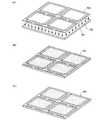
本実施例では、1枚の基板上に複数の半導体装置を形成する場合において、モールドを用いてパターンを形成する例について説明する。 In this embodiment, an example in which a pattern is formed using a mold when a plurality of semiconductor devices are formed over one substrate will be described.
図11(A)に、レジスト702が形成された基板701と、モールド703の様子を示す。モールド703には、各半導体装置に対応したパターンが形成されている。そして、レジスト702にモールド703を押し付け、レジスト702にパターンを形成する。 FIG. 11A shows the state of the
次にモールド703をレジスト702から取り外す。図11(B)に、パターンが形成された後の、レジスト702の様子を示す。次に図11(C)に示すように、パターンが形成されたレジスト702の表面を、アッシング等で削ることで、レジストマスク704を形成する。 Next, the
なお本実施例では、モールドを用いて大型基板に一回でパターンを形成する例を示したが、本発明はこの構成に限定されない。大型基板に複数回に分けてモールドを押し付け、パターンを形成するようにしても良い。ただしこの場合、光ナノインプリント法を用い、パターンを形成する領域を順に選択的に露光するようにする。 In the present embodiment, an example is shown in which a pattern is formed on a large substrate once using a mold, but the present invention is not limited to this configuration. A pattern may be formed by pressing a mold on a large substrate several times. However, in this case, the photo nanoimprint method is used to selectively expose the region where the pattern is formed in order.
フォトリソグラフィ法を用いる場合、基板が大型化するとフォトマスクの価格もそれに伴って上昇してしまう。さらに一度に露光できる面積が限られているので、パターニングにかかるトータルの時間も長くなるという問題があった。しかし本発明のようにナノインプリント法を用いる場合、フォトマスクを用いる必要はなく、さらにパターンを形成する基板が大型化しても、パターンを形成するのにかかる時間を抑えることができる。 When the photolithography method is used, the price of the photomask increases with an increase in the size of the substrate. Furthermore, since the area that can be exposed at one time is limited, there is a problem that the total time required for patterning becomes longer. However, when the nanoimprint method is used as in the present invention, it is not necessary to use a photomask, and even if the substrate on which the pattern is formed becomes larger, the time required to form the pattern can be suppressed.
本実施例は、上記実施の形態1乃至4または実施例1と組み合わせて実施することが可能である。 This example can be implemented in combination with any of Embodiment Modes 1 to 4 or Example 1.
本発明の作製方法を用いて形成される半導体装置は、様々な電子機器に用いることができる。具体的に本発明を用いた電子機器として、ビデオカメラ、デジタルカメラ、ゴーグル型ディスプレイ(ヘッドマウントディスプレイ)、ナビゲーションシステム、音響再生装置(カーオーディオ、オーディオコンポ等)、パーソナルコンピュータ、ゲーム機器、携帯情報端末(モバイルコンピュータ、携帯電話、携帯型ゲーム機または電子書籍等)、記録媒体を備えた画像再生装置(代表的にはDVD:Digital Versatile Disc等の記録媒体を再生し、その画像を表示しうるディスプレイを有する装置)などが挙げられる。これら電子機器の具体例を図12に示す。 A semiconductor device formed using the manufacturing method of the present invention can be used for various electronic devices. Specifically, as an electronic device using the present invention, a video camera, a digital camera, a goggle type display (head mounted display), a navigation system, a sound reproduction device (car audio, audio component, etc.), a personal computer, a game device, portable information A terminal (mobile computer, mobile phone, portable game machine, electronic book, etc.), an image playback device (typically a DVD: Digital Versatile Disc, etc.) provided with a recording medium, and can display the image A device having a display). Specific examples of these electronic devices are shown in FIGS.
図12(A)はパーソナルコンピュータであり、本体2101、表示部2102、操作キー2103、スピーカー部2104等を含む。本発明を用いた半導体装置は、表示部2102及びその他信号処理用の回路に用いることができる。 FIG. 12A illustrates a personal computer, which includes a
図12(B)はゴーグル型表示装置であり、本体2201、表示部2202、イヤホン2203、支持部2204とを有している。本発明を用いた半導体装置は、表示部2202及びその他信号処理用の回路に用いることができる。支持部2204は、ゴーグル型表示装置を頭部自体に固定するタイプであっても良いし、使用者の身体のうち、頭部以外の部分に固定するタイプであっても良い。 FIG. 12B illustrates a goggle type display device, which includes a
図12(C)は表示装置であり、筐体2401、表示部2402、スピーカー部2403等を含む。本発明を用いた半導体装置は、表示部2402及びその他信号処理用の回路に用いることができる。なお、表示装置には、パーソナルコンピュータ用、TV放送受信用、広告表示用などの全ての情報表示用表示装置が含まれる。 FIG. 12C illustrates a display device, which includes a
以上の様に、本発明の適用範囲は極めて広く、あらゆる分野の電子機器に用いることが可能である。また本実施例は、上記実施の形態1乃至4または実施例1、2と組み合わせて実施することが可能である。 As described above, the applicable range of the present invention is so wide that it can be used for electronic devices in various fields. In addition, this embodiment can be implemented in combination with Embodiment Modes 1 to 4 or Embodiments 1 and 2.
101 基板
102 被パターニング層
103 レジスト
104 モールド
105 レジストマスク
101
Claims (5)
Translated fromJapanese減圧雰囲気下で、第1の凹部と、前記第1の凹部の中に形成された第2の凹部とを有するモールドを、前記レジストに押し付けた状態で前記レジストを硬化させた後、超音波を用いて前記レジストに振動を加えながら前記モールドを前記レジストから取り外すことによって、前記第1の凹部及び前記第2の凹部の形状に応じた第1の凸部及び第2の凸部を有するパターンを前記レジストに形成し、
前記パターンが形成された前記レジストの表面を前記導電膜の一部が露出するまでアッシングし、
前記アッシングされた前記レジストをマスクとして用い、前記導電膜をエッチングすることで、段差を有するゲート電極を形成することを特徴とする半導体装置の作製方法。A gate insulating film, a conductive film, and a resist are sequentially formed over the island-shaped semiconductor film,
In a reduced pressure atmosphere, after curing the resist in a state where a mold having a first recess and a second recess formed in the first recess is pressed against the resist, ultrasonic waves are applied. A pattern having first and second convex portions corresponding to the shapes of the first concave portion and the second concave portion is obtained by removing the mold from the resist while applying vibration to the resist. Forming on the resist;
Ashing the surface of the resist on which the pattern is formed until a part of the conductive film is exposed,
A method for manufacturing a semiconductor device, wherein a gate electrode having a step is formed by etching the conductive film using the ashed resist as a mask.
第1の凹部と、前記第1の凹部の中に形成された第2の凹部とを有するモールドを、前記レジストに押し付けた状態で前記レジストを硬化させた後、超音波を用いて前記レジストに振動を加えながら前記モールドを前記レジストから取り外すことによって、前記第1の凹部及び前記第2の凹部の形状に応じた第1の凸部及び第2の凸部を有するパターンを前記レジストに形成し、
前記パターンが形成された前記レジストの表面を前記導電膜の一部が露出するまでアッシングし、
前記アッシングされた前記レジストをマスクとして用い、前記導電膜をエッチングすることで、段差を有するゲート電極を形成することを特徴とする半導体装置の作製方法。A gate insulating film, a conductive film, and a resist are sequentially formed over the island-shaped semiconductor film,
A mold having a first recess and a second recess formed in the first recess is cured in a state where the mold is pressed against the resist, and then is applied to the resist using ultrasonic waves. By removing the mold from the resist while applying vibration, a pattern having first and second convex portions corresponding to the shapes of the first concave portion and the second concave portion is formed on the resist. ,
Ashing the surface of the resist on which the pattern is formed until a part of the conductive film is exposed,
A method for manufacturing a semiconductor device, wherein a gate electrode having a step is formed by etching the conductive film using the ashed resist as a mask.
前記ゲート電極をマスクとして用い、前記島状の半導体膜に不純物をドーピングすることで、前記島状の半導体膜に、チャネル形成領域と、前記チャネル形成領域を間に挟んでいる一対のLDD領域と、前記チャネル形成領域及び前記一対のLDD領域を間に挟んでいるソース領域及びドレイン領域とを形成することを特徴とする半導体装置の作製方法。In claim 1or claim2 ,
By using the gate electrode as a mask and doping the island-shaped semiconductor film with an impurity, the island-shaped semiconductor film has a channel formation region and a pair of LDD regions sandwiching the channel formation region therebetween. A method for manufacturing a semiconductor device is characterized in that a source region and a drain region sandwiching the channel formation region and the pair of LDD regions are formed.
前記レジストは光硬化性樹脂を用いており、紫外線の照射により前記レジストが硬化することを特徴とする半導体装置の作製方法。In any one of Claims 1 thru | or3 ,
A method for manufacturing a semiconductor device, wherein the resist uses a photocurable resin, and the resist is cured by irradiation with ultraviolet rays.
前記レジストは熱可塑性樹脂を用いており、加熱により前記レジストを軟化させてから前記モールドを前記レジストに押し付け、前記モールドを押しつけた状態で前記レジストを冷却して硬化させることを特徴とする半導体装置の作製方法。In any one of Claims 1 thru | or3 ,
The resist uses a thermoplastic resin, softens the resist by heating, presses the mold against the resist, and cools and hardens the resist while the mold is pressed. Manufacturing method.
Priority Applications (1)
| Application Number | Priority Date | Filing Date | Title |
|---|---|---|---|
| JP2005148009AJP4954498B2 (en) | 2004-06-01 | 2005-05-20 | Method for manufacturing semiconductor device |
Applications Claiming Priority (3)
| Application Number | Priority Date | Filing Date | Title |
|---|---|---|---|
| JP2004163172 | 2004-06-01 | ||
| JP2004163172 | 2004-06-01 | ||
| JP2005148009AJP4954498B2 (en) | 2004-06-01 | 2005-05-20 | Method for manufacturing semiconductor device |
Publications (3)
| Publication Number | Publication Date |
|---|---|
| JP2006019707A JP2006019707A (en) | 2006-01-19 |
| JP2006019707A5 JP2006019707A5 (en) | 2008-06-05 |
| JP4954498B2true JP4954498B2 (en) | 2012-06-13 |
Family
ID=35793629
Family Applications (1)
| Application Number | Title | Priority Date | Filing Date |
|---|---|---|---|
| JP2005148009AExpired - Fee RelatedJP4954498B2 (en) | 2004-06-01 | 2005-05-20 | Method for manufacturing semiconductor device |
Country Status (1)
| Country | Link |
|---|---|
| JP (1) | JP4954498B2 (en) |
Families Citing this family (15)
| Publication number | Priority date | Publication date | Assignee | Title |
|---|---|---|---|---|
| EP1984545A4 (en)* | 2006-02-17 | 2013-05-15 | Univ California | PROCESS FOR THE PRODUCTION OF N-TYPE SEMIPOLAR OPTOELECTRONIC DEVICES (AL, IN, GA, B) |
| JP4952009B2 (en)* | 2006-03-23 | 2012-06-13 | 凸版印刷株式会社 | Method for producing imprint mold |
| KR101261606B1 (en)* | 2006-05-09 | 2013-05-09 | 삼성디스플레이 주식회사 | Apparatus for manufacturing a display panel and method for manufacturing the same |
| JP4966586B2 (en)* | 2006-05-24 | 2012-07-04 | 東芝機械株式会社 | Transfer device |
| JP4407673B2 (en) | 2006-07-10 | 2010-02-03 | セイコーエプソン株式会社 | Bank structure, electronic circuit, electronic device manufacturing method, and pattern forming method |
| JP2008155344A (en)* | 2006-12-26 | 2008-07-10 | Hitachi Chem Co Ltd | Liquid photopolymerizable composition, nano-structure with same and manufacturing method therefor |
| CN104076600B (en)* | 2008-01-25 | 2019-02-15 | 旭化成株式会社 | Method for manufacturing seamless mold |
| KR101557816B1 (en) | 2008-09-01 | 2015-10-07 | 삼성디스플레이 주식회사 | Resist composition and method for forming patterns using the same |
| JP2010182824A (en)* | 2009-02-04 | 2010-08-19 | Toshiba Corp | Method of manufacturing magnetic random access memory, and method of manufacturing embedded memory |
| JP5667748B2 (en)* | 2009-03-18 | 2015-02-12 | 株式会社東芝 | Light transmissive solar cell and method for manufacturing the same |
| JP5667747B2 (en) | 2009-03-18 | 2015-02-12 | 株式会社東芝 | Thin film solar cell and manufacturing method thereof |
| JP2011053013A (en)* | 2009-08-31 | 2011-03-17 | Nof Corp | Method of inspecting nanoimprint molding laminate |
| NL2003950C2 (en)* | 2009-12-11 | 2011-06-15 | Panalytical Bv | METHOD FOR MANUFACTURING A MULTI-LAYER STRUCTURE WITH A LATERAL PATTERN FOR USE IN THE XUV WAVE LENGTH AREA AND BT AND LMAG STRUCTURES MANUFACTURED BY THIS METHOD. |
| CN103765987B (en)* | 2011-07-01 | 2016-05-04 | 王子控股株式会社 | Manufacturing method of organic light emitting diode, organic light emitting diode, image display device, lighting device, and substrate |
| JP7414597B2 (en)* | 2020-03-12 | 2024-01-16 | キオクシア株式会社 | Wiring formation method |
Family Cites Families (11)
| Publication number | Priority date | Publication date | Assignee | Title |
|---|---|---|---|---|
| US6482742B1 (en)* | 2000-07-18 | 2002-11-19 | Stephen Y. Chou | Fluid pressure imprint lithography |
| JP2000194142A (en)* | 1998-12-25 | 2000-07-14 | Fujitsu Ltd | Pattern forming method and semiconductor device manufacturing method |
| JP2001277200A (en)* | 2000-03-30 | 2001-10-09 | Toshiba Corp | Micro processing equipment |
| JP4239439B2 (en)* | 2000-07-06 | 2009-03-18 | セイコーエプソン株式会社 | OPTICAL DEVICE, ITS MANUFACTURING METHOD, AND OPTICAL TRANSMISSION DEVICE |
| JP4954401B2 (en)* | 2000-08-11 | 2012-06-13 | 株式会社半導体エネルギー研究所 | Manufacturing method of semiconductor device |
| JP2002134756A (en)* | 2000-10-26 | 2002-05-10 | Matsushita Electric Ind Co Ltd | Semiconductor device and manufacturing method thereof |
| JP3850718B2 (en)* | 2001-11-22 | 2006-11-29 | 株式会社東芝 | Processing method |
| US6653030B2 (en)* | 2002-01-23 | 2003-11-25 | Hewlett-Packard Development Company, L.P. | Optical-mechanical feature fabrication during manufacture of semiconductors and other micro-devices and nano-devices that include micron and sub-micron features |
| JP3848303B2 (en)* | 2002-06-07 | 2006-11-22 | キヤノン株式会社 | Structure, functional structure, and method of manufacturing magnetic recording medium |
| JP3821069B2 (en)* | 2002-08-01 | 2006-09-13 | 株式会社日立製作所 | Method for forming structure by transfer pattern |
| JP2004071934A (en)* | 2002-08-08 | 2004-03-04 | Kanegafuchi Chem Ind Co Ltd | Method for manufacturing fine pattern and transfer material |
- 2005
- 2005-05-20JPJP2005148009Apatent/JP4954498B2/ennot_activeExpired - Fee Related
Also Published As
| Publication number | Publication date |
|---|---|
| JP2006019707A (en) | 2006-01-19 |
Similar Documents
| Publication | Publication Date | Title |
|---|---|---|
| CN1722366B (en) | Method for manufacturing semiconductor device | |
| JP5393726B2 (en) | Method for manufacturing semiconductor device | |
| JP4850858B2 (en) | Method for manufacturing semiconductor device | |
| JP5072157B2 (en) | Method for manufacturing semiconductor device | |
| TWI480984B (en) | Semiconductor device and method of manufacturing the same | |
| JP4954498B2 (en) | Method for manufacturing semiconductor device | |
| TW200305218A (en) | Method of manufacturing a semiconductor device | |
| JP2003051446A (en) | Method for manufacturing semiconductor device | |
| JP4549751B2 (en) | Method for manufacturing semiconductor device | |
| JP4209638B2 (en) | Method for manufacturing semiconductor device | |
| JP4230160B2 (en) | Method for manufacturing semiconductor device | |
| JP4860055B2 (en) | Method for manufacturing semiconductor device | |
| JP4216003B2 (en) | Method for manufacturing semiconductor device | |
| US8048749B2 (en) | Method for manufacturing semiconductor device | |
| JP4176362B2 (en) | Method for manufacturing semiconductor device | |
| JP4212844B2 (en) | Method for manufacturing semiconductor device | |
| JP2003142402A (en) | Method for manufacturing semiconductor device | |
| JP5005881B2 (en) | Method for manufacturing semiconductor device | |
| JP4939699B2 (en) | Method for manufacturing semiconductor device | |
| JP4342843B2 (en) | Method for manufacturing semiconductor device | |
| JP4357811B2 (en) | Method for manufacturing semiconductor device | |
| JP4837871B2 (en) | Method for manufacturing semiconductor device | |
| CN100485872C (en) | Method for preparing amorphous semiconductor film and semiconductor device | |
| JP4267253B2 (en) | Method for manufacturing semiconductor device | |
| JP4176366B2 (en) | Method for manufacturing semiconductor device |
Legal Events
| Date | Code | Title | Description |
|---|---|---|---|
| A521 | Written amendment | Free format text:JAPANESE INTERMEDIATE CODE: A523 Effective date:20080421 | |
| A621 | Written request for application examination | Free format text:JAPANESE INTERMEDIATE CODE: A621 Effective date:20080421 | |
| A977 | Report on retrieval | Free format text:JAPANESE INTERMEDIATE CODE: A971007 Effective date:20110728 | |
| A131 | Notification of reasons for refusal | Free format text:JAPANESE INTERMEDIATE CODE: A131 Effective date:20110802 | |
| A521 | Written amendment | Free format text:JAPANESE INTERMEDIATE CODE: A523 Effective date:20110923 | |
| A02 | Decision of refusal | Free format text:JAPANESE INTERMEDIATE CODE: A02 Effective date:20111115 | |
| A521 | Written amendment | Free format text:JAPANESE INTERMEDIATE CODE: A523 Effective date:20120206 | |
| A911 | Transfer of reconsideration by examiner before appeal (zenchi) | Free format text:JAPANESE INTERMEDIATE CODE: A911 Effective date:20120213 | |
| TRDD | Decision of grant or rejection written | ||
| A01 | Written decision to grant a patent or to grant a registration (utility model) | Free format text:JAPANESE INTERMEDIATE CODE: A01 Effective date:20120313 | |
| A01 | Written decision to grant a patent or to grant a registration (utility model) | Free format text:JAPANESE INTERMEDIATE CODE: A01 | |
| A61 | First payment of annual fees (during grant procedure) | Free format text:JAPANESE INTERMEDIATE CODE: A61 Effective date:20120314 | |
| R150 | Certificate of patent or registration of utility model | Free format text:JAPANESE INTERMEDIATE CODE: R150 | |
| FPAY | Renewal fee payment (event date is renewal date of database) | Free format text:PAYMENT UNTIL: 20150323 Year of fee payment:3 | |
| FPAY | Renewal fee payment (event date is renewal date of database) | Free format text:PAYMENT UNTIL: 20150323 Year of fee payment:3 | |
| R250 | Receipt of annual fees | Free format text:JAPANESE INTERMEDIATE CODE: R250 | |
| R250 | Receipt of annual fees | Free format text:JAPANESE INTERMEDIATE CODE: R250 | |
| R250 | Receipt of annual fees | Free format text:JAPANESE INTERMEDIATE CODE: R250 | |
| LAPS | Cancellation because of no payment of annual fees |