JP4949719B2 - Semiconductor device and manufacturing method thereof - Google Patents
Semiconductor device and manufacturing method thereofDownload PDFInfo
- Publication number
- JP4949719B2 JP4949719B2JP2006106237AJP2006106237AJP4949719B2JP 4949719 B2JP4949719 B2JP 4949719B2JP 2006106237 AJP2006106237 AJP 2006106237AJP 2006106237 AJP2006106237 AJP 2006106237AJP 4949719 B2JP4949719 B2JP 4949719B2
- Authority
- JP
- Japan
- Prior art keywords
- semiconductor device
- polishing
- protruding electrode
- manufacturing
- resin layer
- Prior art date
- Legal status (The legal status is an assumption and is not a legal conclusion. Google has not performed a legal analysis and makes no representation as to the accuracy of the status listed.)
- Expired - Fee Related
Links
- 239000004065semiconductorSubstances0.000titleclaimsdescription65
- 238000004519manufacturing processMethods0.000titleclaimsdescription19
- 238000005498polishingMethods0.000claimsdescription29
- 239000011347resinSubstances0.000claimsdescription27
- 229920005989resinPolymers0.000claimsdescription27
- 230000003746surface roughnessEffects0.000claimsdescription22
- 238000000034methodMethods0.000claimsdescription17
- 229910000679solderInorganic materials0.000claimsdescription16
- 239000002245particleSubstances0.000claimsdescription12
- 229910003460diamondInorganic materials0.000claimsdescription7
- 239000010432diamondSubstances0.000claimsdescription7
- 238000007789sealingMethods0.000claimsdescription6
- RYGMFSIKBFXOCR-UHFFFAOYSA-NCopperChemical compound[Cu]RYGMFSIKBFXOCR-UHFFFAOYSA-N0.000claimsdescription4
- 239000006061abrasive grainSubstances0.000claimsdescription4
- 229910052802copperInorganic materials0.000claimsdescription4
- 239000010949copperSubstances0.000claimsdescription4
- 241000287463PhalacrocoraxSpecies0.000claims1
- 239000000758substrateSubstances0.000description19
- 229910052751metalInorganic materials0.000description11
- 239000002184metalSubstances0.000description11
- 239000002002slurrySubstances0.000description6
- 239000011800void materialSubstances0.000description6
- CURLTUGMZLYLDI-UHFFFAOYSA-NCarbon dioxideChemical compoundO=C=OCURLTUGMZLYLDI-UHFFFAOYSA-N0.000description5
- 239000004575stoneSubstances0.000description4
- 238000012360testing methodMethods0.000description3
- XLYOFNOQVPJJNP-UHFFFAOYSA-NwaterChemical compoundOXLYOFNOQVPJJNP-UHFFFAOYSA-N0.000description3
- 230000015572biosynthetic processEffects0.000description2
- 229910002092carbon dioxideInorganic materials0.000description2
- 239000001569carbon dioxideSubstances0.000description2
- 239000013078crystalSubstances0.000description2
- 239000012535impuritySubstances0.000description2
- 238000007747platingMethods0.000description2
- BASFCYQUMIYNBI-UHFFFAOYSA-NplatinumChemical compound[Pt]BASFCYQUMIYNBI-UHFFFAOYSA-N0.000description2
- 239000004593EpoxySubstances0.000description1
- XUIMIQQOPSSXEZ-UHFFFAOYSA-NSiliconChemical compound[Si]XUIMIQQOPSSXEZ-UHFFFAOYSA-N0.000description1
- BQCADISMDOOEFD-UHFFFAOYSA-NSilverChemical compound[Ag]BQCADISMDOOEFD-UHFFFAOYSA-N0.000description1
- 230000001133accelerationEffects0.000description1
- 229910052782aluminiumInorganic materials0.000description1
- XAGFODPZIPBFFR-UHFFFAOYSA-NaluminiumChemical compound[Al]XAGFODPZIPBFFR-UHFFFAOYSA-N0.000description1
- 238000006243chemical reactionMethods0.000description1
- 238000009713electroplatingMethods0.000description1
- PCHJSUWPFVWCPO-UHFFFAOYSA-NgoldChemical compound[Au]PCHJSUWPFVWCPO-UHFFFAOYSA-N0.000description1
- 229910052737goldInorganic materials0.000description1
- 239000010931goldSubstances0.000description1
- 239000000463materialSubstances0.000description1
- 238000005259measurementMethods0.000description1
- 238000012986modificationMethods0.000description1
- 230000004048modificationEffects0.000description1
- 238000000206photolithographyMethods0.000description1
- 229910052697platinumInorganic materials0.000description1
- 238000007517polishing processMethods0.000description1
- 229910052710siliconInorganic materials0.000description1
- 239000010703siliconSubstances0.000description1
- 229910052709silverInorganic materials0.000description1
- 239000004332silverSubstances0.000description1
- 238000004544sputter depositionMethods0.000description1
- 230000008646thermal stressEffects0.000description1
- 238000001721transfer mouldingMethods0.000description1
Images


Classifications
- H—ELECTRICITY
- H01—ELECTRIC ELEMENTS
- H01L—SEMICONDUCTOR DEVICES NOT COVERED BY CLASS H10
- H01L21/00—Processes or apparatus adapted for the manufacture or treatment of semiconductor or solid state devices or of parts thereof
- H01L21/70—Manufacture or treatment of devices consisting of a plurality of solid state components formed in or on a common substrate or of parts thereof; Manufacture of integrated circuit devices or of parts thereof
- H01L21/71—Manufacture of specific parts of devices defined in group H01L21/70
- H01L21/768—Applying interconnections to be used for carrying current between separate components within a device comprising conductors and dielectrics
- H01L21/76801—Applying interconnections to be used for carrying current between separate components within a device comprising conductors and dielectrics characterised by the formation and the after-treatment of the dielectrics, e.g. smoothing
- H01L21/76819—Smoothing of the dielectric
- H—ELECTRICITY
- H01—ELECTRIC ELEMENTS
- H01L—SEMICONDUCTOR DEVICES NOT COVERED BY CLASS H10
- H01L21/00—Processes or apparatus adapted for the manufacture or treatment of semiconductor or solid state devices or of parts thereof
- H01L21/70—Manufacture or treatment of devices consisting of a plurality of solid state components formed in or on a common substrate or of parts thereof; Manufacture of integrated circuit devices or of parts thereof
- H01L21/71—Manufacture of specific parts of devices defined in group H01L21/70
- H01L21/768—Applying interconnections to be used for carrying current between separate components within a device comprising conductors and dielectrics
- H01L21/76838—Applying interconnections to be used for carrying current between separate components within a device comprising conductors and dielectrics characterised by the formation and the after-treatment of the conductors
- H01L21/7684—Smoothing; Planarisation
- H—ELECTRICITY
- H01—ELECTRIC ELEMENTS
- H01L—SEMICONDUCTOR DEVICES NOT COVERED BY CLASS H10
- H01L23/00—Details of semiconductor or other solid state devices
- H01L23/28—Encapsulations, e.g. encapsulating layers, coatings, e.g. for protection
- H01L23/31—Encapsulations, e.g. encapsulating layers, coatings, e.g. for protection characterised by the arrangement or shape
- H01L23/3107—Encapsulations, e.g. encapsulating layers, coatings, e.g. for protection characterised by the arrangement or shape the device being completely enclosed
- H01L23/3114—Encapsulations, e.g. encapsulating layers, coatings, e.g. for protection characterised by the arrangement or shape the device being completely enclosed the device being a chip scale package, e.g. CSP
- H—ELECTRICITY
- H01—ELECTRIC ELEMENTS
- H01L—SEMICONDUCTOR DEVICES NOT COVERED BY CLASS H10
- H01L24/00—Arrangements for connecting or disconnecting semiconductor or solid-state bodies; Methods or apparatus related thereto
- H01L24/01—Means for bonding being attached to, or being formed on, the surface to be connected, e.g. chip-to-package, die-attach, "first-level" interconnects; Manufacturing methods related thereto
- H01L24/10—Bump connectors ; Manufacturing methods related thereto
- H01L24/11—Manufacturing methods
- H—ELECTRICITY
- H01—ELECTRIC ELEMENTS
- H01L—SEMICONDUCTOR DEVICES NOT COVERED BY CLASS H10
- H01L24/00—Arrangements for connecting or disconnecting semiconductor or solid-state bodies; Methods or apparatus related thereto
- H01L24/01—Means for bonding being attached to, or being formed on, the surface to be connected, e.g. chip-to-package, die-attach, "first-level" interconnects; Manufacturing methods related thereto
- H01L24/10—Bump connectors ; Manufacturing methods related thereto
- H01L24/12—Structure, shape, material or disposition of the bump connectors prior to the connecting process
- H—ELECTRICITY
- H01—ELECTRIC ELEMENTS
- H01L—SEMICONDUCTOR DEVICES NOT COVERED BY CLASS H10
- H01L2224/00—Indexing scheme for arrangements for connecting or disconnecting semiconductor or solid-state bodies and methods related thereto as covered by H01L24/00
- H01L2224/01—Means for bonding being attached to, or being formed on, the surface to be connected, e.g. chip-to-package, die-attach, "first-level" interconnects; Manufacturing methods related thereto
- H01L2224/02—Bonding areas; Manufacturing methods related thereto
- H01L2224/023—Redistribution layers [RDL] for bonding areas
- H01L2224/0231—Manufacturing methods of the redistribution layers
- H—ELECTRICITY
- H01—ELECTRIC ELEMENTS
- H01L—SEMICONDUCTOR DEVICES NOT COVERED BY CLASS H10
- H01L2224/00—Indexing scheme for arrangements for connecting or disconnecting semiconductor or solid-state bodies and methods related thereto as covered by H01L24/00
- H01L2224/01—Means for bonding being attached to, or being formed on, the surface to be connected, e.g. chip-to-package, die-attach, "first-level" interconnects; Manufacturing methods related thereto
- H01L2224/02—Bonding areas; Manufacturing methods related thereto
- H01L2224/04—Structure, shape, material or disposition of the bonding areas prior to the connecting process
- H01L2224/0401—Bonding areas specifically adapted for bump connectors, e.g. under bump metallisation [UBM]
- H—ELECTRICITY
- H01—ELECTRIC ELEMENTS
- H01L—SEMICONDUCTOR DEVICES NOT COVERED BY CLASS H10
- H01L2224/00—Indexing scheme for arrangements for connecting or disconnecting semiconductor or solid-state bodies and methods related thereto as covered by H01L24/00
- H01L2224/01—Means for bonding being attached to, or being formed on, the surface to be connected, e.g. chip-to-package, die-attach, "first-level" interconnects; Manufacturing methods related thereto
- H01L2224/10—Bump connectors; Manufacturing methods related thereto
- H01L2224/12—Structure, shape, material or disposition of the bump connectors prior to the connecting process
- H01L2224/13—Structure, shape, material or disposition of the bump connectors prior to the connecting process of an individual bump connector
- H01L2224/13001—Core members of the bump connector
- H01L2224/1301—Shape
- H01L2224/13011—Shape comprising apertures or cavities, e.g. hollow bump
- H—ELECTRICITY
- H01—ELECTRIC ELEMENTS
- H01L—SEMICONDUCTOR DEVICES NOT COVERED BY CLASS H10
- H01L2224/00—Indexing scheme for arrangements for connecting or disconnecting semiconductor or solid-state bodies and methods related thereto as covered by H01L24/00
- H01L2224/01—Means for bonding being attached to, or being formed on, the surface to be connected, e.g. chip-to-package, die-attach, "first-level" interconnects; Manufacturing methods related thereto
- H01L2224/10—Bump connectors; Manufacturing methods related thereto
- H01L2224/12—Structure, shape, material or disposition of the bump connectors prior to the connecting process
- H01L2224/13—Structure, shape, material or disposition of the bump connectors prior to the connecting process of an individual bump connector
- H01L2224/13001—Core members of the bump connector
- H01L2224/13099—Material
- H—ELECTRICITY
- H01—ELECTRIC ELEMENTS
- H01L—SEMICONDUCTOR DEVICES NOT COVERED BY CLASS H10
- H01L2224/00—Indexing scheme for arrangements for connecting or disconnecting semiconductor or solid-state bodies and methods related thereto as covered by H01L24/00
- H01L2224/01—Means for bonding being attached to, or being formed on, the surface to be connected, e.g. chip-to-package, die-attach, "first-level" interconnects; Manufacturing methods related thereto
- H01L2224/10—Bump connectors; Manufacturing methods related thereto
- H01L2224/15—Structure, shape, material or disposition of the bump connectors after the connecting process
- H01L2224/16—Structure, shape, material or disposition of the bump connectors after the connecting process of an individual bump connector
- H—ELECTRICITY
- H01—ELECTRIC ELEMENTS
- H01L—SEMICONDUCTOR DEVICES NOT COVERED BY CLASS H10
- H01L2924/00—Indexing scheme for arrangements or methods for connecting or disconnecting semiconductor or solid-state bodies as covered by H01L24/00
- H01L2924/01—Chemical elements
- H01L2924/01005—Boron [B]
- H—ELECTRICITY
- H01—ELECTRIC ELEMENTS
- H01L—SEMICONDUCTOR DEVICES NOT COVERED BY CLASS H10
- H01L2924/00—Indexing scheme for arrangements or methods for connecting or disconnecting semiconductor or solid-state bodies as covered by H01L24/00
- H01L2924/01—Chemical elements
- H01L2924/01006—Carbon [C]
- H—ELECTRICITY
- H01—ELECTRIC ELEMENTS
- H01L—SEMICONDUCTOR DEVICES NOT COVERED BY CLASS H10
- H01L2924/00—Indexing scheme for arrangements or methods for connecting or disconnecting semiconductor or solid-state bodies as covered by H01L24/00
- H01L2924/01—Chemical elements
- H01L2924/01013—Aluminum [Al]
- H—ELECTRICITY
- H01—ELECTRIC ELEMENTS
- H01L—SEMICONDUCTOR DEVICES NOT COVERED BY CLASS H10
- H01L2924/00—Indexing scheme for arrangements or methods for connecting or disconnecting semiconductor or solid-state bodies as covered by H01L24/00
- H01L2924/01—Chemical elements
- H01L2924/01029—Copper [Cu]
- H—ELECTRICITY
- H01—ELECTRIC ELEMENTS
- H01L—SEMICONDUCTOR DEVICES NOT COVERED BY CLASS H10
- H01L2924/00—Indexing scheme for arrangements or methods for connecting or disconnecting semiconductor or solid-state bodies as covered by H01L24/00
- H01L2924/01—Chemical elements
- H01L2924/01033—Arsenic [As]
- H—ELECTRICITY
- H01—ELECTRIC ELEMENTS
- H01L—SEMICONDUCTOR DEVICES NOT COVERED BY CLASS H10
- H01L2924/00—Indexing scheme for arrangements or methods for connecting or disconnecting semiconductor or solid-state bodies as covered by H01L24/00
- H01L2924/01—Chemical elements
- H01L2924/01047—Silver [Ag]
- H—ELECTRICITY
- H01—ELECTRIC ELEMENTS
- H01L—SEMICONDUCTOR DEVICES NOT COVERED BY CLASS H10
- H01L2924/00—Indexing scheme for arrangements or methods for connecting or disconnecting semiconductor or solid-state bodies as covered by H01L24/00
- H01L2924/01—Chemical elements
- H01L2924/01075—Rhenium [Re]
- H—ELECTRICITY
- H01—ELECTRIC ELEMENTS
- H01L—SEMICONDUCTOR DEVICES NOT COVERED BY CLASS H10
- H01L2924/00—Indexing scheme for arrangements or methods for connecting or disconnecting semiconductor or solid-state bodies as covered by H01L24/00
- H01L2924/01—Chemical elements
- H01L2924/01078—Platinum [Pt]
- H—ELECTRICITY
- H01—ELECTRIC ELEMENTS
- H01L—SEMICONDUCTOR DEVICES NOT COVERED BY CLASS H10
- H01L2924/00—Indexing scheme for arrangements or methods for connecting or disconnecting semiconductor or solid-state bodies as covered by H01L24/00
- H01L2924/01—Chemical elements
- H01L2924/01079—Gold [Au]
- H—ELECTRICITY
- H01—ELECTRIC ELEMENTS
- H01L—SEMICONDUCTOR DEVICES NOT COVERED BY CLASS H10
- H01L2924/00—Indexing scheme for arrangements or methods for connecting or disconnecting semiconductor or solid-state bodies as covered by H01L24/00
- H01L2924/013—Alloys
- H01L2924/014—Solder alloys
- H—ELECTRICITY
- H01—ELECTRIC ELEMENTS
- H01L—SEMICONDUCTOR DEVICES NOT COVERED BY CLASS H10
- H01L2924/00—Indexing scheme for arrangements or methods for connecting or disconnecting semiconductor or solid-state bodies as covered by H01L24/00
- H01L2924/10—Details of semiconductor or other solid state devices to be connected
- H01L2924/11—Device type
- H01L2924/14—Integrated circuits
- H—ELECTRICITY
- H01—ELECTRIC ELEMENTS
- H01L—SEMICONDUCTOR DEVICES NOT COVERED BY CLASS H10
- H01L2924/00—Indexing scheme for arrangements or methods for connecting or disconnecting semiconductor or solid-state bodies as covered by H01L24/00
- H01L2924/30—Technical effects
- H01L2924/35—Mechanical effects
- H01L2924/351—Thermal stress
Landscapes
- Engineering & Computer Science (AREA)
- Microelectronics & Electronic Packaging (AREA)
- Computer Hardware Design (AREA)
- Power Engineering (AREA)
- Physics & Mathematics (AREA)
- Condensed Matter Physics & Semiconductors (AREA)
- General Physics & Mathematics (AREA)
- Manufacturing & Machinery (AREA)
- Mechanical Treatment Of Semiconductor (AREA)
- Structures Or Materials For Encapsulating Or Coating Semiconductor Devices Or Solid State Devices (AREA)
Description
Translated fromJapanese本発明は、半導体装置の製造方法、特に、突起電極を備えた半導体装置の製造方法に関するものである。 The present invention relates to a method for manufacturing a semiconductor device, and more particularly to a method for manufacturing a semiconductor device provided with a protruding electrode.
近年、軽簿短小のニーズから、配線ピッチ幅の縮小化の傾向にある。従来、半導体集積回路の配線工程において、研磨砥粒等の化学反応物質を含むスラリーを用いて、半導体基板面を研磨する方法が開示されている(例えば、特許文献1参照)。 In recent years, there is a tendency to reduce the wiring pitch width due to the need for a short book. Conventionally, in a wiring process of a semiconductor integrated circuit, a method of polishing a semiconductor substrate surface using a slurry containing a chemical reaction material such as polishing abrasive grains has been disclosed (for example, see Patent Document 1).
しかしながら、特許文献1に開示された方法では、配線ピッチ幅の縮小化を実現するとしても、スラリーから起因する不純物(酸性)の影響により、金属部分が湿気に弱くなる。
そこで、配線ピッチ幅の縮小化を実現しつつ、湿気に強い半導体装置が望まれていた。However, in the method disclosed in
Therefore, there has been a demand for a semiconductor device that is resistant to moisture while reducing the wiring pitch width.
この発明の半導体装置の製造方法は、前述の課題を解決するために、半導体チップ上に突起電極を形成するステップと、突起電極および半導体チップを樹脂層で封止するステップとを含む。さらに、突起電極の上面が露出するまで樹脂層を第1研磨するステップと、露出した突起電極の上面の面粗度が30nm以下になるように、前記露出した突起電極の上面及び前記樹脂層を第2研磨するステップと、第2研磨した突起電極の上面に半田端子を形成するステップとを含む。
この発明の半導体装置の製造方法は、スラリーを用いることなく、半導体チップ上に形成された突起電極の上面を第1研磨した後、その上面をさらに第2研磨する。In order to solve the above-described problems, a method of manufacturing a semiconductor device according to the present invention includes a step of forming a protruding electrode on a semiconductorchip and a step of sealing the protruding electrode and the semiconductorchip with a resin layer. Further, the first polishing of the resin layer until the upper surface of the protruding electrode is exposed, and the upper surface of the exposed protruding electrode and the resin layerare adjusted so that the surface roughness of the exposed upper surfaceof the protruding electrodeis 30 nm or less. A second polishing step and a step of forming a solder terminal on the upper surface of the second polished protruding electrode.
In the method for manufacturing a semiconductor device according to the present invention, the upper surface of the protruding electrode formed on the semiconductor chip is first polished without using slurry, and then the upper surface is further polished.
この発明によれば、半導体チップ上に形成された突起電極の上面を第1研磨および第2研磨により研磨したため、突起電極の上面が、スラリーを用いることなく平滑になり、配線ピッチ幅の縮小化を実現しつつ、湿気に強い半導体装置が得られる。 According to the present invention, since the upper surface of the protruding electrode formed on the semiconductor chip is polished by the first polishing and the second polishing, the upper surface of the protruding electrode becomes smooth without using slurry, and the wiring pitch width is reduced. Thus, a moisture-resistant semiconductor device can be obtained.
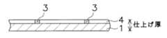
図1は本発明の実施の形態に係る半導体装置の一構成例を示す断面図である。ここでは、CSP(Chip Size Package)の場合を例にして説明するが、これに限られない。図1には、半導体基板上の半導体チップ1を含む半導体装置の一部の断面が示されている。半導体基板として、例えば、厚さが500μm程度のシリコン基板を用いる。
図1において、半導体装置100は、半導体チップ1と、メタルパッド2と、ポスト(突起電極)3と、樹脂層(封止層)4と、半田端子5とを含んで構成されている。FIG. 1 is a cross-sectional view showing a configuration example of a semiconductor device according to an embodiment of the present invention. Here, a case of CSP (Chip Size Package) will be described as an example, but the present invention is not limited to this. FIG. 1 shows a partial cross section of a semiconductor device including a
In FIG. 1, the
具体的には、半導体チップ1の周囲には、複数のメタルパッド2が所定の間隔で形成されている。そして、半導体チップ1の主面(図1では上面)、つまり回路形成面には、配線6を介して、ポスト3が形成されている。
ポスト3は、配線6を介して、メタルパッド2と電気的に接続されている。ポスト3は、たとえば銅で柱状に形成されている。なお、ポスト3の面粗度は、30nm以下になっているが、この点は後記する。
また、ポスト3の側面31および半導体チップ1の主面は、樹脂層4で封止されている。樹脂層4は、たとえばエポキシ等で形成されている。Specifically, a plurality of
The
Further, the side surface 31 of the
次に、実施の形態に係る半導体装置100の製造方法について図2Aないし図2Eに基づいて説明する。
まず、半導体基板上の半導体チップ1の上面に、たとえば電気メッキ等でポスト3を形成する(図2A参照)。具体的には、このとき、半導体チップ1の上面には、論理回路が形成されており、半導体チップ1の周辺には、メタルパッド(不図示)が形成されている。そして、この半導体チップ1の主面(図2では上面)全体に対して、絶縁膜(不図示)を形成する。絶縁膜は、例えばフォトリソグラフィなどの処理により形成する。次に、メタルパッド2および上記絶縁膜の表面に対して、例えばスパッタ法などの処理により再配線(図1の配線6に相当)を形成する。その後、その再配線の所定の位置にポスト3を形成する。この形成は、例えば銅による金属メッキ法を用いるが、アルミニウム、金、銀または白金による金属メッキ法を適用してもよい。Next, a method for manufacturing the
First, the
続いて、半導体チップ1の主面およびポスト3を封止するために、樹脂を充填して樹脂層4を形成する(図2B参照)。樹脂の充填は、例えばトランスファーモールド法等を用いる。これにより、樹脂層4がポスト3の上面に積層される。なお、本実施の形態では、図2Bに示したように、上記形成された樹脂層4の上面から半導体チップ1の下面までの厚さを投入厚という。 Subsequently, in order to seal the main surface of the
次に、ポスト3の上面が露出するまで、研磨刃30を用いて、樹脂層4の上面を研磨する(図2C参照:ここでの研磨を第1研磨という)。この場合の研磨条件の一例を表1に示す。なお、「ポスト3の上面が露出するまで」というのは、あらかじめ定められたポスト3の高さに達するまでという意味であり、詳細については後記する。 Next, the upper surface of the

表1によると、1軸(#325)条件および2軸(#600)条件という研磨条件の異なる2段階の研磨が行われる。具体的には、まず、1軸(#325)条件下で、#325の砥石粒子を用いた第1段階の研磨が行われ、次に、2軸(#600)条件下で、#600の砥石粒子を用いた第2段階の研磨が行われる。
ここで、第1段階の研磨について詳述する。第1段階の研磨においては、まず、#325の砥石粒子を用いて、半導体チップ1の下面から樹脂層4の上面までの厚さが、{投入厚−(仕上げ厚+30μm)}になるまで研磨する(1軸条件の研削量1stの欄参照)。仕上げ厚とは、あらかじめ設定された、半導体チップ1の下面から樹脂層4の上面までの厚さを意味する(図2D参照)。この場合、たとえば、砥石回転数を2400rpm、ステージ回転数を200rpm、砥石降下速度を125μm/minとする。According to Table 1, two-stage polishing is performed with different polishing conditions: a uniaxial (# 325) condition and a biaxial (# 600) condition. Specifically, first stage polishing is performed using # 325 grinding stone particles under uniaxial (# 325) conditions, and then # 600 under biaxial (# 600) conditions. A second stage of polishing is performed using the grindstone particles.
Here, the first stage polishing will be described in detail. In the first stage polishing, first, polishing is performed using # 325 grinding stone particles until the thickness from the lower surface of the
続いて、#325の砥石粒子を用いて、20μm分の樹脂層4の樹脂を研磨する。この場合、砥石回転数を2400rpm、ステージ回転数を200rpm、砥石降下速度を50μm/minとする(表1の1軸条件、1stの各欄参照)。 Subsequently, the resin of the
次に、第2段階の研磨について詳述する。第2段階の研磨においては、表1に示したように、#600の砥石粒子を用いて、まず、砥石回転数を3000rpm、ステージ回転数を120rpm、砥石降下速度を30μm/minとして、厚さが10μm分(研削量)の樹脂層4の樹脂を研削する(2軸条件、1stの各欄参照)。
さらに、#600の砥石粒子を用いて、10μm分(研削量)の樹脂層4の樹脂を研削する(表1の2軸条件の研削量2stの欄参照)。この場合、砥石回転数を3000rpm、ステージ回転数を120rpm、砥石降下速度を15μm/minとする(表1の2軸条件、2stの各欄参照)。これにより、ポスト3の高さがあらかじめ定められた高さ(本実施の形態では、表1に示した2軸条件下での研削後のポストの高さ)になる。また、ポスト3の上面がある程度の面粗さ(ここでは、例えば220μm)になる。Next, the second stage polishing will be described in detail. In the second stage polishing, as shown in Table 1, using # 600 grinding stone particles, first, the grinding wheel rotational speed is 3000 rpm, the stage rotational speed is 120 rpm, and the grinding stone lowering speed is 30 μm / min. Is 10 μm (grinding amount) of the resin of the
Further, the resin of the
なお、表1に示した2段階の研磨では、#325の砥石粒子および#600の砥石粒子を用いた場合で説明したが、#300〜#1200のうちのいずれかの砥石粒子を適用してもよい。 In the two-stage polishing shown in Table 1, the case of using # 325 grindstone particles and # 600 grindstone particles has been described, but any one of # 300 to # 1200 grindstone particles is applied. Also good.
次に、例えば、単結晶ダイヤモンドのバイトを用いて、露出したポスト3上面の仕上げ面粗度を30nm以下に研磨する(図2D参照)。この場合の研磨条件の一例を表2に示す。なお、単結晶ダイヤモンドは、ダイヤモンド粒子が#2000のダイヤモンド砥粒を用いるが、例えば、#2000よりも細かいダイヤモンド砥粒を用いてもよい。 Next, for example, using a single crystal diamond tool, the exposed surface roughness of the upper surface of the
表2によると、バイト回転数を2000rpm、ワークピッチ送りを20μm/rev、バイトのスクイ角を0°として、ポスト3の上面および樹脂層4の樹脂を研磨する。これにより、ポスト3上面の仕上げ面粗度を220nm未満、好ましくは30nm以下に仕上げる。 According to Table 2, the upper surface of the
次に、リフローを行い、半田端子5を形成する(図2E参照)。この場合、メタルパッド2の領域には、酸化膜が形成されているので、この酸化膜が、リフロー時に水蒸気や炭酸に還元される。その結果、半田端子5内にボイド8が発生することになる。 Next, reflow is performed to form solder terminals 5 (see FIG. 2E). In this case, since an oxide film is formed in the region of the
その後、ダイシングによりウエハを個片化して、半導体装置100が完成する。なお、このとき、半導体基板1の裏面を樹脂で封止することも可能である。 Thereafter, the wafer is separated into pieces by dicing, and the
その後、半導体装置100を不図示の基板(たとえばマザーボード)に実装する。この場合、温度変化により、半導体装置100と上記基板との間に熱応力が生じ、時間の経過に伴い各半田端子5の接続部から内部に向かってクラックが伸展する。この際、各半田端子5内にボイドがあると、クラックの伸展が加速される。
したがって、ボイド8が大きければ大きいほど、ボイド8が大きく変形し、半田端子5の接続部が断線しやすくなる。また、ボイド8が大きければ大きいほど、半田端子5内部の断面積が小さくなり、半田端子5自体の強度が弱くなる。よって、半田端子5がクラックしやすくなる。このことは、ボイド8の数が多い場合にも同様のことがいえる。
すなわち、ボイド8の数が多ければ多いほど、半田端子5の接続部が断線しやすくなる。また、半田端子5内部の断面積が小さくなり、半田端子5自体の強度も弱くなる。Thereafter, the
Therefore, the larger the
That is, the larger the number of
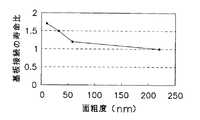
このようにして基板が実装された半導体装置100(つまり製品)に関し、ポスト3上面の面粗度の値を変化させて、基板接続(ここでは、半導体装置100と基板との接続の意味)の寿命比を測定した。その測定結果を表3に示す。なお、ここでは、各面粗度ごとに、計4つの試験条件下で製品の寿命(加速)試験を順次行った。試験条件は、125℃で9分、25℃で1分、−25℃で9分、25℃で1分の順序とした。 Regarding the semiconductor device 100 (that is, the product) on which the substrate is mounted in this manner, the value of the surface roughness on the upper surface of the
表3によると、面粗度が58nmの場合は、面粗度が220nmの場合に比べて、基板接続の寿命比が1.2倍になった。また、面粗度が32nm、10nmの場合は、面粗度が220nmの場合に比べて、それぞれ順に、基板接続の寿命比が1.5倍、1.7倍になった。 According to Table 3, when the surface roughness was 58 nm, the life ratio of the substrate connection was 1.2 times that when the surface roughness was 220 nm. In addition, when the surface roughness was 32 nm and 10 nm, the life ratio of the substrate connection was 1.5 times and 1.7 times, respectively, as compared with the case where the surface roughness was 220 nm.
次に、面粗度を0nm〜220nmの範囲で変化させた場合の上記基板接続の寿命比を示すグラフを図3に示す。図3から、面粗度が220nmよりも小さくなるにつれ、基板接続の寿命比が大きくなることがわかった。つまり、面粗度が小さくなればなるほど、半導体装置100と基板との間の接続の信頼性が向上することがわかった。以上から、面粗度が30nm以下の場合が好適であることがわかった。
これは、次のような理由による。すなわち、ポスト3上面の面粗度が小さくなれば、ポスト3上面の表面積が小さくなるので、上記リフロー時において(図2E参照)、ポスト3に形成される酸化膜の量が少なくなる。したがって、酸化膜に起因する水蒸気や炭酸ガスの発生量も少なくなり、水蒸気や炭酸ガス等で生じるボイド8も小さくなるからである。Next, FIG. 3 shows a graph showing the life ratio of the substrate connection when the surface roughness is changed in the range of 0 nm to 220 nm. FIG. 3 shows that the life ratio of the substrate connection increases as the surface roughness becomes smaller than 220 nm. That is, it has been found that the smaller the surface roughness is, the more reliable the connection between the
This is due to the following reason. That is, if the surface roughness of the upper surface of the
以上のように、本実施の形態では、従来におけるスラリーを用いることなく半導体装置を製造するので、スラリーから起因する不純物(酸性)の影響により、金属部分が湿気に弱いという不都合もない。また、ポスト3の面粗度を好適な30nm以下にするので、基板接続の寿命が比較的延び、基板接続の信頼性が向上する。よって、配線ピッチ幅の縮小化を実現しつつ、湿気に強い半導体装置100を得ることができる。 As described above, in this embodiment, since the semiconductor device is manufactured without using the conventional slurry, there is no inconvenience that the metal portion is vulnerable to moisture due to the influence of impurities (acidity) resulting from the slurry. Further, since the surface roughness of the
なお、本発明は、上記実施の形態に限られるものではなく、種々の変形が可能である。突起電極として、たとえば、ポスト3を用いた場合について説明したが、たとえば、バンプを用いてもよい。また、突起電極の形状も柱状に限られず、たとえば凸状にしてもよい。 The present invention is not limited to the above embodiment, and various modifications can be made. For example, the case where the
100 半導体装置
1 半導体チップ
2 メタルパッド
3 ポスト(突起電極)
4 樹脂層(封止層)
5 半田端子
6 配線DESCRIPTION OF
4 Resin layer (sealing layer)
5
Claims (9)
Translated fromJapanese前記突起電極および前記半導体チップを樹脂層で封止するステップと、
前記突起電極の上面が露出するまで前記樹脂層を第1研磨するステップと、
前記露出した突起電極の上面の面粗度が30nm以下になるように、前記露出した突起電極の上面及び前記樹脂層を第2研磨するステップと、
前記第2研磨した突起電極の上面に半田端子を形成するステップと、を含む、
半導体装置の製造方法。Forming a protruding electrode on a semiconductor chip;
Sealing the protruding electrode and the semiconductorchip with a resin layer;
First polishing the resin layer until an upper surface of the protruding electrode is exposed;
Second polishingthe upper surface of the exposed bump electrode and the resin layer so that the surface roughness of the upper surfaceof the exposed bump electrodeis 30 nm or less ;
Forming a solder terminal on the upper surface of the second polished protruding electrode,
A method for manufacturing a semiconductor device.
請求項1に記載の半導体装置の製造方法。In the first polishing, the surface roughness of the upper surface of the protruding electrodecormorants row polished until 200nm,
A method for manufacturing a semiconductor device according to claim 1.
請求項2に記載の半導体装置の製造方法。In the first polishing, a rotating grindstone is used to perform two-stage polishing with different polishing conditions.
A method for manufacturing a semiconductor device according to claim 2.
請求項3に記載の半導体装置の製造方法。The first polishing is performed under the polishing conditions in which the particles of the rotating grindstone are # 300 to # 1200.
A method for manufacturing a semiconductor device according to claim 3.
請求項1ないし請求項4のいずれか1項に記載の半導体装置の製造方法。In the second polishing, the diamond particles are polished by using diamond abrasive grains that are finer than # 2000.
The method of manufacturing a semiconductor device according to any one of claims1 to 4.
前記半導体チップ上に形成され、かつ上面の面粗度が30nm以下の突起電極と、
前記突起電極の側面よび前記半導体チップの主面を封止する封止層と、
前記面粗度が30nm以下の突起電極の上面に形成された半田端子と、を備えた半導体装置。A semiconductor device manufactured using the method for manufacturing a semiconductor device according to claim 1,
A protruding electrode formed on the semiconductorchip and having an upper surface with asurface roughness of 30 nm or less;
A sealing layer for sealing the side surface of the protruding electrode and the main surface of the semiconductorchip ;
And a solder terminal formed on the upper surface of the protruding electrode having asurface roughness of 30 nm or less.
Priority Applications (2)
| Application Number | Priority Date | Filing Date | Title |
|---|---|---|---|
| JP2006106237AJP4949719B2 (en) | 2006-04-07 | 2006-04-07 | Semiconductor device and manufacturing method thereof |
| US11/652,120US7547624B2 (en) | 2006-04-07 | 2007-01-11 | Semiconductor device and method of producing the same |
Applications Claiming Priority (1)
| Application Number | Priority Date | Filing Date | Title |
|---|---|---|---|
| JP2006106237AJP4949719B2 (en) | 2006-04-07 | 2006-04-07 | Semiconductor device and manufacturing method thereof |
Publications (2)
| Publication Number | Publication Date |
|---|---|
| JP2007281236A JP2007281236A (en) | 2007-10-25 |
| JP4949719B2true JP4949719B2 (en) | 2012-06-13 |
Family
ID=38575867
Family Applications (1)
| Application Number | Title | Priority Date | Filing Date |
|---|---|---|---|
| JP2006106237AExpired - Fee RelatedJP4949719B2 (en) | 2006-04-07 | 2006-04-07 | Semiconductor device and manufacturing method thereof |
Country Status (2)
| Country | Link |
|---|---|
| US (1) | US7547624B2 (en) |
| JP (1) | JP4949719B2 (en) |
Families Citing this family (11)
| Publication number | Priority date | Publication date | Assignee | Title |
|---|---|---|---|---|
| JP2010283109A (en)* | 2009-06-04 | 2010-12-16 | Rohm Co Ltd | Method of manufacturing semiconductor device, and the semiconductor device |
| JP2011018720A (en)* | 2009-07-08 | 2011-01-27 | Casio Computer Co Ltd | Method of manufacturing semiconductor device |
| KR101128063B1 (en) | 2011-05-03 | 2012-04-23 | 테세라, 인코포레이티드 | Package-on-package assembly with wire bonds to encapsulation surface |
| JP2013008898A (en)* | 2011-06-27 | 2013-01-10 | Disco Abrasive Syst Ltd | Processing method of workpiece |
| US8836136B2 (en) | 2011-10-17 | 2014-09-16 | Invensas Corporation | Package-on-package assembly with wire bond vias |
| US8835228B2 (en) | 2012-05-22 | 2014-09-16 | Invensas Corporation | Substrate-less stackable package with wire-bond interconnect |
| US9502390B2 (en) | 2012-08-03 | 2016-11-22 | Invensas Corporation | BVA interposer |
| US9167710B2 (en)* | 2013-08-07 | 2015-10-20 | Invensas Corporation | Embedded packaging with preformed vias |
| US9583456B2 (en) | 2013-11-22 | 2017-02-28 | Invensas Corporation | Multiple bond via arrays of different wire heights on a same substrate |
| US9583411B2 (en) | 2014-01-17 | 2017-02-28 | Invensas Corporation | Fine pitch BVA using reconstituted wafer with area array accessible for testing |
| US9490222B1 (en) | 2015-10-12 | 2016-11-08 | Invensas Corporation | Wire bond wires for interference shielding |
Family Cites Families (5)
| Publication number | Priority date | Publication date | Assignee | Title |
|---|---|---|---|---|
| JP2001094005A (en)* | 1999-09-22 | 2001-04-06 | Oki Electric Ind Co Ltd | Semiconductor device and method for producing it |
| JP3409759B2 (en)* | 1999-12-09 | 2003-05-26 | カシオ計算機株式会社 | Manufacturing method of semiconductor device |
| JP2003234430A (en)* | 2002-02-07 | 2003-08-22 | Casio Micronics Co Ltd | Semiconductor device and its manufacturing method |
| JP2004193488A (en) | 2002-12-13 | 2004-07-08 | Tosoh Corp | Polishing liquid for barrier metal and polishing method |
| JP4052955B2 (en)* | 2003-02-06 | 2008-02-27 | Necエレクトロニクス株式会社 | Manufacturing method of semiconductor device |
- 2006
- 2006-04-07JPJP2006106237Apatent/JP4949719B2/ennot_activeExpired - Fee Related
- 2007
- 2007-01-11USUS11/652,120patent/US7547624B2/ennot_activeExpired - Fee Related
Also Published As
| Publication number | Publication date |
|---|---|
| JP2007281236A (en) | 2007-10-25 |
| US20070238289A1 (en) | 2007-10-11 |
| US7547624B2 (en) | 2009-06-16 |
Similar Documents
| Publication | Publication Date | Title |
|---|---|---|
| JP4949719B2 (en) | Semiconductor device and manufacturing method thereof | |
| US20240186268A1 (en) | Directly bonded structure with frame structure | |
| JP4056854B2 (en) | Manufacturing method of semiconductor device | |
| US9490237B2 (en) | Semiconductor package including a plurality of chips | |
| Rao et al. | TSV interposer fabrication for 3D IC packaging | |
| US20060051900A1 (en) | Method of manufacturing a semiconductor device | |
| US20250112123A1 (en) | Through substrate via structures and processes | |
| US8298944B1 (en) | Warpage control for die with protruding TSV tips during thermo-compressive bonding | |
| TW202211328A (en) | Semiconductor package | |
| TW201019423A (en) | Integrated circuit structures and method of forming the same | |
| JP2006120943A (en) | Chip built-in substrate and its manufacturing method | |
| JP2004282035A (en) | Method of manufacturing semiconductor device | |
| US20170154881A1 (en) | Semiconductor device and method of manufacturing the same | |
| CN102163588A (en) | Semiconductor device and method for manufacturing the same | |
| TW202514831A (en) | Direct bonding methods and structures for dies | |
| JP2005340431A (en) | Method for manufacturing semiconductor device | |
| JP2006229112A (en) | Semiconductor device and manufacturing method thereof | |
| US20120211886A1 (en) | Method for Fabricating a Small Footprint Chip-Scale Package and a Device Made from the Method | |
| KR20070077686A (en) | Wafer level chip scale package with unrestricted bump pads and method of manufacturing the same | |
| JP6674281B2 (en) | Package forming method | |
| JP4515177B2 (en) | Wiring formation method | |
| US6955981B2 (en) | Pad structure to prompt excellent bondability for low-k intermetal dielectric layers | |
| CN1755901A (en) | Chemical Mechanical Polishing Process | |
| JPH04370958A (en) | Semiconductor substrate, semiconductor integrated circuit device using the same, and method for manufacturing semiconductor substrate | |
| US6894389B2 (en) | Semiconductor device and manufacturing method therefor |
Legal Events
| Date | Code | Title | Description |
|---|---|---|---|
| A621 | Written request for application examination | Free format text:JAPANESE INTERMEDIATE CODE: A621 Effective date:20080919 | |
| A711 | Notification of change in applicant | Free format text:JAPANESE INTERMEDIATE CODE: A712 Effective date:20081210 | |
| A977 | Report on retrieval | Free format text:JAPANESE INTERMEDIATE CODE: A971007 Effective date:20090120 | |
| RD03 | Notification of appointment of power of attorney | Free format text:JAPANESE INTERMEDIATE CODE: A7423 Effective date:20090206 | |
| A131 | Notification of reasons for refusal | Free format text:JAPANESE INTERMEDIATE CODE: A131 Effective date:20101102 | |
| A521 | Written amendment | Free format text:JAPANESE INTERMEDIATE CODE: A523 Effective date:20101228 | |
| A02 | Decision of refusal | Free format text:JAPANESE INTERMEDIATE CODE: A02 Effective date:20110705 | |
| A01 | Written decision to grant a patent or to grant a registration (utility model) | Free format text:JAPANESE INTERMEDIATE CODE: A01 | |
| A61 | First payment of annual fees (during grant procedure) | Free format text:JAPANESE INTERMEDIATE CODE: A61 Effective date:20120308 | |
| FPAY | Renewal fee payment (event date is renewal date of database) | Free format text:PAYMENT UNTIL: 20150316 Year of fee payment:3 | |
| R150 | Certificate of patent or registration of utility model | Free format text:JAPANESE INTERMEDIATE CODE: R150 | |
| S531 | Written request for registration of change of domicile | Free format text:JAPANESE INTERMEDIATE CODE: R313531 | |
| R350 | Written notification of registration of transfer | Free format text:JAPANESE INTERMEDIATE CODE: R350 | |
| LAPS | Cancellation because of no payment of annual fees |