JP4945185B2 - Crystal growth method - Google Patents
Crystal growth methodDownload PDFInfo
- Publication number
- JP4945185B2 JP4945185B2JP2006201369AJP2006201369AJP4945185B2JP 4945185 B2JP4945185 B2JP 4945185B2JP 2006201369 AJP2006201369 AJP 2006201369AJP 2006201369 AJP2006201369 AJP 2006201369AJP 4945185 B2JP4945185 B2JP 4945185B2
- Authority
- JP
- Japan
- Prior art keywords
- gas
- substrate
- crystal growth
- susceptor
- rotating shaft
- Prior art date
- Legal status (The legal status is an assumption and is not a legal conclusion. Google has not performed a legal analysis and makes no representation as to the accuracy of the status listed.)
- Expired - Fee Related
Links
Images


Classifications
- C—CHEMISTRY; METALLURGY
- C30—CRYSTAL GROWTH
- C30B—SINGLE-CRYSTAL GROWTH; UNIDIRECTIONAL SOLIDIFICATION OF EUTECTIC MATERIAL OR UNIDIRECTIONAL DEMIXING OF EUTECTOID MATERIAL; REFINING BY ZONE-MELTING OF MATERIAL; PRODUCTION OF A HOMOGENEOUS POLYCRYSTALLINE MATERIAL WITH DEFINED STRUCTURE; SINGLE CRYSTALS OR HOMOGENEOUS POLYCRYSTALLINE MATERIAL WITH DEFINED STRUCTURE; AFTER-TREATMENT OF SINGLE CRYSTALS OR A HOMOGENEOUS POLYCRYSTALLINE MATERIAL WITH DEFINED STRUCTURE; APPARATUS THEREFOR
- C30B29/00—Single crystals or homogeneous polycrystalline material with defined structure characterised by the material or by their shape
- C30B29/10—Inorganic compounds or compositions
- C30B29/40—AIIIBV compounds wherein A is B, Al, Ga, In or Tl and B is N, P, As, Sb or Bi
- C—CHEMISTRY; METALLURGY
- C23—COATING METALLIC MATERIAL; COATING MATERIAL WITH METALLIC MATERIAL; CHEMICAL SURFACE TREATMENT; DIFFUSION TREATMENT OF METALLIC MATERIAL; COATING BY VACUUM EVAPORATION, BY SPUTTERING, BY ION IMPLANTATION OR BY CHEMICAL VAPOUR DEPOSITION, IN GENERAL; INHIBITING CORROSION OF METALLIC MATERIAL OR INCRUSTATION IN GENERAL
- C23C—COATING METALLIC MATERIAL; COATING MATERIAL WITH METALLIC MATERIAL; SURFACE TREATMENT OF METALLIC MATERIAL BY DIFFUSION INTO THE SURFACE, BY CHEMICAL CONVERSION OR SUBSTITUTION; COATING BY VACUUM EVAPORATION, BY SPUTTERING, BY ION IMPLANTATION OR BY CHEMICAL VAPOUR DEPOSITION, IN GENERAL
- C23C16/00—Chemical coating by decomposition of gaseous compounds, without leaving reaction products of surface material in the coating, i.e. chemical vapour deposition [CVD] processes
- C23C16/44—Chemical coating by decomposition of gaseous compounds, without leaving reaction products of surface material in the coating, i.e. chemical vapour deposition [CVD] processes characterised by the method of coating
- C23C16/455—Chemical coating by decomposition of gaseous compounds, without leaving reaction products of surface material in the coating, i.e. chemical vapour deposition [CVD] processes characterised by the method of coating characterised by the method used for introducing gases into reaction chamber or for modifying gas flows in reaction chamber
- C23C16/45563—Gas nozzles
- C23C16/45572—Cooled nozzles
- C—CHEMISTRY; METALLURGY
- C23—COATING METALLIC MATERIAL; COATING MATERIAL WITH METALLIC MATERIAL; CHEMICAL SURFACE TREATMENT; DIFFUSION TREATMENT OF METALLIC MATERIAL; COATING BY VACUUM EVAPORATION, BY SPUTTERING, BY ION IMPLANTATION OR BY CHEMICAL VAPOUR DEPOSITION, IN GENERAL; INHIBITING CORROSION OF METALLIC MATERIAL OR INCRUSTATION IN GENERAL
- C23C—COATING METALLIC MATERIAL; COATING MATERIAL WITH METALLIC MATERIAL; SURFACE TREATMENT OF METALLIC MATERIAL BY DIFFUSION INTO THE SURFACE, BY CHEMICAL CONVERSION OR SUBSTITUTION; COATING BY VACUUM EVAPORATION, BY SPUTTERING, BY ION IMPLANTATION OR BY CHEMICAL VAPOUR DEPOSITION, IN GENERAL
- C23C16/00—Chemical coating by decomposition of gaseous compounds, without leaving reaction products of surface material in the coating, i.e. chemical vapour deposition [CVD] processes
- C23C16/44—Chemical coating by decomposition of gaseous compounds, without leaving reaction products of surface material in the coating, i.e. chemical vapour deposition [CVD] processes characterised by the method of coating
- C23C16/455—Chemical coating by decomposition of gaseous compounds, without leaving reaction products of surface material in the coating, i.e. chemical vapour deposition [CVD] processes characterised by the method of coating characterised by the method used for introducing gases into reaction chamber or for modifying gas flows in reaction chamber
- C23C16/45563—Gas nozzles
- C23C16/45576—Coaxial inlets for each gas
- C—CHEMISTRY; METALLURGY
- C23—COATING METALLIC MATERIAL; COATING MATERIAL WITH METALLIC MATERIAL; CHEMICAL SURFACE TREATMENT; DIFFUSION TREATMENT OF METALLIC MATERIAL; COATING BY VACUUM EVAPORATION, BY SPUTTERING, BY ION IMPLANTATION OR BY CHEMICAL VAPOUR DEPOSITION, IN GENERAL; INHIBITING CORROSION OF METALLIC MATERIAL OR INCRUSTATION IN GENERAL
- C23C—COATING METALLIC MATERIAL; COATING MATERIAL WITH METALLIC MATERIAL; SURFACE TREATMENT OF METALLIC MATERIAL BY DIFFUSION INTO THE SURFACE, BY CHEMICAL CONVERSION OR SUBSTITUTION; COATING BY VACUUM EVAPORATION, BY SPUTTERING, BY ION IMPLANTATION OR BY CHEMICAL VAPOUR DEPOSITION, IN GENERAL
- C23C16/00—Chemical coating by decomposition of gaseous compounds, without leaving reaction products of surface material in the coating, i.e. chemical vapour deposition [CVD] processes
- C23C16/44—Chemical coating by decomposition of gaseous compounds, without leaving reaction products of surface material in the coating, i.e. chemical vapour deposition [CVD] processes characterised by the method of coating
- C23C16/458—Chemical coating by decomposition of gaseous compounds, without leaving reaction products of surface material in the coating, i.e. chemical vapour deposition [CVD] processes characterised by the method of coating characterised by the method used for supporting substrates in the reaction chamber
- C23C16/4582—Rigid and flat substrates, e.g. plates or discs
- C23C16/4583—Rigid and flat substrates, e.g. plates or discs the substrate being supported substantially horizontally
- C23C16/4584—Rigid and flat substrates, e.g. plates or discs the substrate being supported substantially horizontally the substrate being rotated
- C—CHEMISTRY; METALLURGY
- C30—CRYSTAL GROWTH
- C30B—SINGLE-CRYSTAL GROWTH; UNIDIRECTIONAL SOLIDIFICATION OF EUTECTIC MATERIAL OR UNIDIRECTIONAL DEMIXING OF EUTECTOID MATERIAL; REFINING BY ZONE-MELTING OF MATERIAL; PRODUCTION OF A HOMOGENEOUS POLYCRYSTALLINE MATERIAL WITH DEFINED STRUCTURE; SINGLE CRYSTALS OR HOMOGENEOUS POLYCRYSTALLINE MATERIAL WITH DEFINED STRUCTURE; AFTER-TREATMENT OF SINGLE CRYSTALS OR A HOMOGENEOUS POLYCRYSTALLINE MATERIAL WITH DEFINED STRUCTURE; APPARATUS THEREFOR
- C30B25/00—Single-crystal growth by chemical reaction of reactive gases, e.g. chemical vapour-deposition growth
- C30B25/02—Epitaxial-layer growth
- C30B25/16—Controlling or regulating
- C30B25/165—Controlling or regulating the flow of the reactive gases
- C—CHEMISTRY; METALLURGY
- C30—CRYSTAL GROWTH
- C30B—SINGLE-CRYSTAL GROWTH; UNIDIRECTIONAL SOLIDIFICATION OF EUTECTIC MATERIAL OR UNIDIRECTIONAL DEMIXING OF EUTECTOID MATERIAL; REFINING BY ZONE-MELTING OF MATERIAL; PRODUCTION OF A HOMOGENEOUS POLYCRYSTALLINE MATERIAL WITH DEFINED STRUCTURE; SINGLE CRYSTALS OR HOMOGENEOUS POLYCRYSTALLINE MATERIAL WITH DEFINED STRUCTURE; AFTER-TREATMENT OF SINGLE CRYSTALS OR A HOMOGENEOUS POLYCRYSTALLINE MATERIAL WITH DEFINED STRUCTURE; APPARATUS THEREFOR
- C30B29/00—Single crystals or homogeneous polycrystalline material with defined structure characterised by the material or by their shape
- C30B29/10—Inorganic compounds or compositions
- C30B29/40—AIIIBV compounds wherein A is B, Al, Ga, In or Tl and B is N, P, As, Sb or Bi
- C30B29/403—AIII-nitrides
- H—ELECTRICITY
- H01—ELECTRIC ELEMENTS
- H01L—SEMICONDUCTOR DEVICES NOT COVERED BY CLASS H10
- H01L21/00—Processes or apparatus adapted for the manufacture or treatment of semiconductor or solid state devices or of parts thereof
- H01L21/02—Manufacture or treatment of semiconductor devices or of parts thereof
- H01L21/02104—Forming layers
- H01L21/02365—Forming inorganic semiconducting materials on a substrate
- H01L21/02518—Deposited layers
- H01L21/02521—Materials
- H01L21/02538—Group 13/15 materials
- H01L21/0254—Nitrides
- H—ELECTRICITY
- H01—ELECTRIC ELEMENTS
- H01L—SEMICONDUCTOR DEVICES NOT COVERED BY CLASS H10
- H01L21/00—Processes or apparatus adapted for the manufacture or treatment of semiconductor or solid state devices or of parts thereof
- H01L21/02—Manufacture or treatment of semiconductor devices or of parts thereof
- H01L21/02104—Forming layers
- H01L21/02365—Forming inorganic semiconducting materials on a substrate
- H01L21/02518—Deposited layers
- H01L21/0257—Doping during depositing
- H01L21/02573—Conductivity type
- H01L21/02579—P-type
- H—ELECTRICITY
- H01—ELECTRIC ELEMENTS
- H01L—SEMICONDUCTOR DEVICES NOT COVERED BY CLASS H10
- H01L21/00—Processes or apparatus adapted for the manufacture or treatment of semiconductor or solid state devices or of parts thereof
- H01L21/02—Manufacture or treatment of semiconductor devices or of parts thereof
- H01L21/02104—Forming layers
- H01L21/02365—Forming inorganic semiconducting materials on a substrate
- H01L21/02612—Formation types
- H01L21/02617—Deposition types
- H01L21/0262—Reduction or decomposition of gaseous compounds, e.g. CVD
- Y—GENERAL TAGGING OF NEW TECHNOLOGICAL DEVELOPMENTS; GENERAL TAGGING OF CROSS-SECTIONAL TECHNOLOGIES SPANNING OVER SEVERAL SECTIONS OF THE IPC; TECHNICAL SUBJECTS COVERED BY FORMER USPC CROSS-REFERENCE ART COLLECTIONS [XRACs] AND DIGESTS
- Y10—TECHNICAL SUBJECTS COVERED BY FORMER USPC
- Y10T—TECHNICAL SUBJECTS COVERED BY FORMER US CLASSIFICATION
- Y10T117/00—Single-crystal, oriented-crystal, and epitaxy growth processes; non-coating apparatus therefor
- Y10T117/10—Apparatus
- Y10T117/1016—Apparatus with means for treating single-crystal [e.g., heat treating]
Landscapes
- Chemical & Material Sciences (AREA)
- Engineering & Computer Science (AREA)
- Metallurgy (AREA)
- Organic Chemistry (AREA)
- Materials Engineering (AREA)
- General Chemical & Material Sciences (AREA)
- Chemical Kinetics & Catalysis (AREA)
- Manufacturing & Machinery (AREA)
- Physics & Mathematics (AREA)
- Condensed Matter Physics & Semiconductors (AREA)
- General Physics & Mathematics (AREA)
- Crystallography & Structural Chemistry (AREA)
- Computer Hardware Design (AREA)
- Microelectronics & Electronic Packaging (AREA)
- Power Engineering (AREA)
- Mechanical Engineering (AREA)
- Inorganic Chemistry (AREA)
- Chemical Vapour Deposition (AREA)
- Crystals, And After-Treatments Of Crystals (AREA)
Description
Translated fromJapanese本発明は、結晶成長方法に関する。 The present invention relates to a crystal growth method.
有機金属気相成長法(MOCVD:Metal-Organic Chemical Vapor Deposition)は、膜厚や組成の制御性などに優れているために化合物半導体の結晶成長に利用されている。しかし、例えばGaNなどの窒化物半導体を成長させる場合、AlGaAs系やInAlGaP系材料と比べて、より高い結晶成長温度が必要とされるため、種々の問題が生じる。 Metal-organic chemical vapor deposition (MOCVD) is used for crystal growth of compound semiconductors because of its excellent film thickness and composition controllability. However, when growing a nitride semiconductor such as GaN, for example, a higher crystal growth temperature is required as compared with AlGaAs-based and InAlGaP-based materials, and various problems arise.
例えば、ウェーハをほぼ水平に保持し、原料ガス及びキャリアガスの流れ方向がウェーハとほぼ平行ないわゆる横フロー方式において、ガスは結晶成長チャンバの中心近傍に設けられるノズルから放出される。この場合、ガスの上流側における温度を十分には低くできないために、ガスの熱分解及びこれに伴う中間反応が生ずる。この結果、ウェーハ近傍では原料元素が不足傾向となり、半導体膜成長速度は最大値より低下することが多い。 For example, in a so-called lateral flow method in which the wafer is held almost horizontally and the flow directions of the source gas and carrier gas are substantially parallel to the wafer, the gas is discharged from a nozzle provided near the center of the crystal growth chamber. In this case, since the temperature on the upstream side of the gas cannot be sufficiently lowered, thermal decomposition of the gas and accompanying intermediate reaction occur. As a result, the raw material elements tend to be insufficient in the vicinity of the wafer, and the semiconductor film growth rate often decreases from the maximum value.
特に、トリメチルアルミニウム及びアンモニアの分解に伴う中間反応の結果、下流側においてアルミニウム(Al)が不足する。この結果、Al組成比を大きくするのが困難となるなどの問題を生じる。 In particular, as a result of an intermediate reaction accompanying the decomposition of trimethylaluminum and ammonia, aluminum (Al) is insufficient on the downstream side. As a result, there arises a problem that it is difficult to increase the Al composition ratio.
ウェーハ内における結晶成長膜の均質性や制御性を改善する技術開示例がある(特許文献1)。これは、AlGaAs系材料などにおいて、サセプタ中心部からウェーハまでの領域温度を基板上より低く制御することにより、電子移動度の均一性を改善しようとするものである。しかしながら、窒化物系材料ではより結晶成長温度が高いので、さらなる改善が必要である。
本発明は、原料ガスの中間反応が低減された結晶成長方法を提供する。 The present invention provides a crystal growth method in which an intermediate reaction of a source gas is reduced.
本発明の一態様によれば、回転シャフトと、前記回転シャフトと連動する基板載置部を有し、前記基板載置部に載置された基板を前記回転シャフトの回転軸のまわりに公転させるサセプタと、前記サセプタに載置された前記基板を加熱するヒータと、前記回転軸の側から、前記基板の主面に対して平行な方向に原料ガスを放出する複数のノズルと、前記ノズルと対向するように前記回転シャフトに連結され、前記サセプタの熱伝導率よりも高い熱伝導率を有する熱伝導部材と、内縁部と外縁部とを有し、断熱材からなる第1の熱遮断手段であって、前記内縁部が前記熱伝導部材に連結され、前記外縁部が前記サセプタに連結された第1の熱遮断手段と、赤外線反射体を有し、前記ヒータと前記回転シャフトとの間の空間に設けられた第2の熱遮断手段と、を有する結晶成長装置を用いた結晶成長方法であって、前記基板を前記回転軸のまわりに自公転させつつ、前記回転軸の側から前記基板の主面に対して平行な方向に原料ガスおよびキャリアガスを流し、前記原料ガスは第1のガスと第2のガスとを含み、前記第1のガスと前記キャリアガスとの混合ガスと、前記第2のガスと前記キャリアガスとの混合ガスと、は、前記複数のノズルの異なる吹き出し口から分離して吹き出され、前記原料ガスの熱分解により形成される窒化物系半導体膜の成長速度が最大となる位置よりも前記基板の中心が前記回転軸の側となるように配置して前記窒化物系半導体膜を形成することを特徴とする結晶成長方法が提供される。According to an aspect of the present invention, therotating shaft and the substrate mounting portion interlocked with the rotating shaft are provided, and the substrate mounted on the substrate mounting portion is revolved around the rotation axis of the rotating shaft. A susceptor, a heater for heating the substrate mounted on the susceptor, a plurality of nozzles for discharging a source gas in a direction parallel to the main surface of the substrate from the rotating shaft side, and the nozzle A first heat-blocking means comprising a heat conductive member connected to the rotating shaft so as to face each other and having a heat conductivity higher than that of the susceptor, an inner edge portion and an outer edge portion, and made of a heat insulating material. The inner edge portion is connected to the heat conducting member, the outer edge portion is connected to the susceptor, and includes an infrared reflector, between the heater and the rotating shaft. The second heat provided in the space The cross-sectional unit, a crystal growth method using the crystal growth apparatus having, whilerevolvingthe substrate aroundthe rotation axis, a direction parallel to the principal surface of the substrate from the side of the rotary shaft A source gas and a carrier gas are allowed to flow, thesource gas includes a first gas and a second gas, a mixed gas of the first gas and the carrier gas, the second gas and the carrier gas And the mixed gas is blown separately from different outlets of the plurality of nozzles, and the substrate is located at a position where the growth rate of thenitride-based semiconductor film formed by thermal decomposition of the source gas is maximized. A crystal growth method is provided in which the nitride-based semiconductor film is formed so as to be arranged so that its center is on the rotation axis side.
本発明により、原料ガスの中間反応が低減された結晶成長方法が提供される。
According to the present invention, there is provided a crystal growth method in which an intermediate reaction of a source gas is reduced.
以下、図面を参照しつつ本発明の実施の形態について説明する。
図1は、本発明の実施の形態にかかる結晶成長方法を説明するための模式図である。すなわち、同図(a)は結晶成長装置において複数の基板50が保持されたサセプタ12の模式平面図であり、同図(b)は、サセプタの中心から半径方向にみた半導体膜の成長速度の分布を表すグラフ図である。Hereinafter, embodiments of the present invention will be described with reference to the drawings.
FIG. 1 is a schematic diagram for explaining a crystal growth method according to an embodiment of the present invention. That is, FIG. 4A is a schematic plan view of the
化合物半導体を結晶成長するための横フロー型MOCVD装置においては、結晶成長膜の均一性を良くするために、複数個の基板50が配置されたサセプタ12を回転軸の周りに回転させる。すなわち、図1(a)に例示したように、半導体材料などからなる複数の基板50をサセプタ12上に載置する。そして、サセプタ12は、回転中心であるP点の周りを矢印K(あるいはその逆)の向きに回転する。従って、それぞれの基板50は、P点を中心として公転する。 In a lateral flow type MOCVD apparatus for crystal growth of a compound semiconductor, the
一方、ノズル42は固定されており、原料ガスおよびキャリアガスは半径方向の距離RNに位置するノズル42の吹き出し口から、基板50の主面に対してほぼ平行に半径方向Rに向かって周囲に吹き出す。なお、図1(a)においては、一方向へのガス流のみを表している。 On the other hand, the
基板50の公転運動により、ノズル42からのガス流及びサセプタ12の温度の円周方向分布を平均化でき、円周方向における膜厚や特性の変動を抑制できる。また、複数の基板50の上に結晶成長される半導体膜の膜厚や特性を基板間で揃えるために、これら基板50の中心はP点から半径方向にほぼ等距離である位置RWとなるように揃える。またさらに、これら基板50をそれぞれ矢印G(あるいはその逆)の方向に自転させることにより、基板内での膜厚や特性を均一にすることができる。 By the revolving motion of the
ヒータにより基板50を加熱すると、横フローにより供給された原料ガスが熱分解され、結晶成長温度以上において半導体膜が成長する。この場合、サセプタ12の温度分布と、原料ガスの供給量の分布とにより半導体膜の成長速度がほぼ決まる。 When the
図1(b)において成長速度を表す実線は、成長速度が最大となる位置RGよりも回転軸に近い側においては、半径方向距離Rの増加とともに成長速度が増大する領域Aと、位置RGよりも外側において距離Rの増加に伴い成長速度が減少する領域Bと、を有する。ここで、領域Aは半径方向に遠ざかるにつれて成長原料の供給が増大する領域であり、領域Bは半径方向に遠ざかるにつれて成長原料が枯渇する領域であることを表している。成長速度は、R1≦R≦R2の領域Mにおいては概ね直線的に増大し、領域QにおけるRGで最大となるように飽和し、領域Nにおいて成長速度が概ね直線的に低下する。領域Mの回転軸側と領域Nの外側では、成長速度は相対的に急峻に低下する。本実施形態においては、基板50の中心RWが、半導体膜の成長速度が最大となる位置RGよりも回転軸の側となるようにして結晶成長を行う。 In FIG. 1B, the solid line representing the growth rate is based on the region A where the growth rate increases with the increase of the radial distance R on the side closer to the rotation axis than the position RG where the growth rate is maximum, and the position RG. Also has a region B in which the growth rate decreases as the distance R increases on the outside. Here, the region A is a region where the supply of the growth raw material increases as it moves away in the radial direction, and the region B represents a region where the growth raw material is depleted as it moves away in the radial direction. The growth rate increases substantially linearly in the region M where R1 ≦ R ≦ R2, saturates so as to become the maximum in RG in the region Q, and the growth rate decreases substantially linearly in the region N. On the rotation axis side of the region M and outside the region N, the growth rate decreases relatively steeply. In the present embodiment, crystal growth is performed such that the center RW of the
これとは逆に、成長速度が最大となる位置RGよりも基板50の中心RWが外側となるように配置して結晶成長を行うと、基板50からみてガス上流部、すなわちサセプタ12の回転軸に近い部分においてサセプタ12や結晶成長装置内への成長膜の堆積物が増加する。この堆積物が分解または脱離し基板50に再付着すると、成長膜の表面にピット(穴)や荒れなどが生じて成長膜の品質や特性が低下する。 On the contrary, when crystal growth is performed with the center RW of the
これに対して、本実施形態においては、基板50の中心RWを位置RGよりも回転軸に近い側に配置することにより、基板50よりもガス上流側における結晶成長装置内への堆積物を低減できるので、ピットや荒れなどを低減し成長膜の品質及び特性を改善できる。 On the other hand, in the present embodiment, by placing the center RW of the
またさらに、基板50のほぼ全体を図1(b)に例示される領域M内に配置して自転させれば、半径方向における成長速度の変動を平均化し成長膜の均一性をさらに高めることができる。すなわち、領域Mにおいては、成長速度は概ね直線的に変化する分布を有するので、この領域Mにおいて基板50を自転させると、成長膜の厚みや特性の分布を均一にすることができる。 Furthermore, if almost the
図1(b)に例示した成長速度曲線の領域A内に基板50の中心がおさまるように配置して結晶成長を行うための方法としては、原料ガスの総流量を増加する方法を挙げることができる。このようにすると、領域Aを拡げて、成長速度が最大となる位置RGをガス下流側へ移動させることができる。
また一方、上流側の温度を下げる方法も挙げることができる。上流側の温度を下げると、上流側において原料ガスの熱分解を抑制できるので、成長速度が最大となる位置RGをガス下流側に移動させ、領域Aを拡げることが可能となる。As a method for performing crystal growth by arranging the center of the
On the other hand, a method of lowering the temperature on the upstream side can also be mentioned. If the temperature on the upstream side is lowered, the thermal decomposition of the raw material gas can be suppressed on the upstream side, so that the position RG where the growth rate is maximized can be moved to the gas downstream side and the region A can be expanded.
本実施形態によれば、成長膜の品質や均一性を改善させる効果の他にも、原料ガスの低減効果や、混晶比を上げる効果、不純物の高濃度化の効果なども得ることが可能となる。 According to the present embodiment, in addition to the effect of improving the quality and uniformity of the growth film, it is possible to obtain the effect of reducing the source gas, the effect of increasing the mixed crystal ratio, the effect of increasing the concentration of impurities, and the like. It becomes.
すなわちまず、基板50の中心RWを位置RGよりも回転軸に近い側に配置することにより、基板よりも上流側における原料ガスの熱分解や中間反応を抑制できるので、この部分への堆積物の付着を抑制でき、原料ガスの無駄を低減できる。 That is, first, by disposing the center RW of the
次に、窒化物系半導体材料を例に挙げ、アルミニウム(Al)組成比をより高くできる効果について説明する。
図2は、Al原料の供給比に対する成長膜のAl組成比の依存性を例示するグラフ図であり、同図(a)は成長速度が半径方向距離Rに対して低下する領域Bで結晶成長した比較例、同図(b)は図1(b)に例示した領域Aで成長した具体例を表す。Next, the effect of increasing the aluminum (Al) composition ratio will be described using a nitride semiconductor material as an example.
FIG. 2 is a graph illustrating the dependence of the Al composition ratio of the growth film on the supply ratio of the Al raw material. FIG. 2A shows crystal growth in a region B where the growth rate decreases with respect to the radial distance R. The comparative example shown in FIG. 6B shows a specific example of growth in the region A exemplified in FIG.
比較例においては、堆積種が基板に到達する前にAl原料と他の原料との中間反応が激しく生じるので基板の近傍ではAl元素が枯渇し、Al組成比がAl原料供給比に比例せず飽和する。Alは例えばGaなどと比較して反応性が高いためにこの傾向が顕著に生ずると考えられる。そして、Al原料供給比をさらに増加するとAl組成比はむしろ低下する。また、チャンバ内の圧力を高くしてもAl組成比が低下する。 In the comparative example, the intermediate reaction between the Al raw material and the other raw material occurs vigorously before the deposition species reaches the substrate, so the Al element is depleted in the vicinity of the substrate, and the Al composition ratio is not proportional to the Al raw material supply ratio. Saturates. This tendency is considered to occur remarkably because Al is more reactive than Ga, for example. If the Al raw material supply ratio is further increased, the Al composition ratio is rather lowered. Moreover, even if the pressure in the chamber is increased, the Al composition ratio decreases.
これに対して、図1(b)に例示したように領域Aで成長させると、基板の上流側で中間反応が生ずる領域が大幅に縮小される。つまり、Al原料元素が枯渇していないので、基板に成長した成長膜のAl組成比をAl原料供給比の増大に応じて高くすることができる。この結果として、InGaAlNなどにおいて、Al組成比をより高くすることが可能となる。なお、中間反応を抑制するには、上流部近傍の温度を概ね500℃以下とすることがより効果的である。また、材料は窒化物系半導体材料に限定されず、InGaAlP系、AlGaAs系材料であっても同様の効果が得られる。 On the other hand, when the growth is performed in the region A as illustrated in FIG. 1B, the region in which the intermediate reaction occurs on the upstream side of the substrate is significantly reduced. That is, since the Al source element is not depleted, the Al composition ratio of the growth film grown on the substrate can be increased as the Al source supply ratio increases. As a result, the Al composition ratio can be further increased in InGaAlN or the like. In order to suppress the intermediate reaction, it is more effective to set the temperature in the vicinity of the upstream portion to approximately 500 ° C. or less. Further, the material is not limited to the nitride-based semiconductor material, and the same effect can be obtained even with an InGaAlP-based material or an AlGaAs-based material.
次に、同じく窒化物系半導体材料を例に挙げ、p型不純物であるマグネシウム(Mg)をInGaAlNなどにドーピングする場合について説明する。
成長速度が半径方向Rに対して低下する領域Bで結晶成長した場合には、図2に関して前述した場合と同様に、Cp2MgなどのMg原料流量に対して、成長膜のMg濃度が比例せずに飽和する。これは、基板の上流側において中間反応によりMgが消費され枯渇するからであると考えられる。また、チャンバの圧力を高くしてもMg濃度は大幅に低下する。
これに対して、図1(b)に例示した領域Aで成長させると、基板の上流側で中間反応が生ずる領域を大幅に縮小できる。その結果として、Mgが枯渇しないので、成長膜のMg濃度をMg原料ガス流量の増大に伴い高くできる。したがって、InGaAlNなどにおいて、Mg濃度をより高くできる。Next, a case of doping magnesium (Mg), which is a p-type impurity, into InGaAlN or the like will be described using a nitride-based semiconductor material as an example.
When the crystal growth is performed in the region B where the growth rate decreases with respect to the radial direction R, the Mg concentration of the growth film is proportional to the Mg raw material flow rate of Cp2 Mg or the like, as described above with reference to FIG. Saturates without. This is presumably because Mg is consumed and depleted by an intermediate reaction on the upstream side of the substrate. Even if the chamber pressure is increased, the Mg concentration is significantly reduced.
On the other hand, when the growth is performed in the region A illustrated in FIG. 1B, the region in which the intermediate reaction occurs on the upstream side of the substrate can be greatly reduced. As a result, since Mg is not depleted, the Mg concentration of the growth film can be increased as the Mg raw material gas flow rate increases. Therefore, Mg concentration can be made higher in InGaAlN or the like.
ところで、本実施形態においては、基板の上流側の温度を下げて、図1(b)に表した領域A内のRN<R<RDなる領域Sにおいて成長速度を急峻に低下させると、上述した各種の効果をさらに顕著にすることが可能となる。すなわち、基板の上流側の温度を低く抑えることにより、その部分での原料ガスの分解や中間反応をさらに抑制できる。その結果として、前述した成長膜の品質改善効果や、原料ガスの低減効果や、混晶比の改善、不純物の高濃度化などをさらに顕著にすることが可能となる。 By the way, in the present embodiment, when the temperature on the upstream side of the substrate is lowered and the growth rate is sharply reduced in the region S where RN <R <RD in the region A shown in FIG. Various effects can be made more prominent. That is, by suppressing the temperature on the upstream side of the substrate to be low, the decomposition of the source gas and the intermediate reaction at that portion can be further suppressed. As a result, the above-described growth film quality improvement effect, source gas reduction effect, mixed crystal ratio improvement, impurity concentration increase, and the like can be made more remarkable.
次に、本実施形態にかかる結晶成長方法を実現するための結晶成長装置について説明する。
図3は、本発明の実施の形態にかかる結晶成長装置の模式断面図である。同図については、図1に関して前述したものと同様の要素には同一の符号を付した。Next, a crystal growth apparatus for realizing the crystal growth method according to the present embodiment will be described.
FIG. 3 is a schematic cross-sectional view of the crystal growth apparatus according to the embodiment of the present invention. In the figure, the same elements as those described above with reference to FIG.
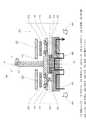
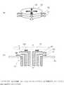
真空チャンバ60の内部には、冷却水46用の通路を有するSUSなどからなるノズル42、ノズル42の下部を囲むように配置された円環状の石英などからなる対向板40、ヒータ24,カーボンなどからなるヒータカバー25、反射体26などが配置されている。また、真空チャンバ60には排気口44が設けられており、反応後の原料ガス及びキャリアガスを排気する。なお、ノズル42は、III族原料ガス、V族原料ガス、キャリアガス、あるいはこれらの混合ガスなどを吹き出すための複数の吹き出し口を有する。ノズル42形状については、後に具体例を挙げて説明する。 Inside the
ノズル45の上方には回転シャフト10が設けられ、ディスク状のサセプタ12が取り付けられている。サセプタ12は、炭化珪素(SiC)が被覆されたカーボンなどからなり、基板の形状に応じた開口部を有する基板載置部を有する。カーボンは加工しやすく、温度範囲も3000℃までと広いためにサセプタ材料として好適である。サセプタ12は、断熱部材(第1の熱遮断手段)20と熱伝導部材22とを介して回転シャフト10に連結され、これら部材と連動して回転する。断熱部材20は、石英などの熱伝導率の低い材料からなる。一方、熱伝導部材22は、サセプタの材料であるカーボンなどよりも熱伝導率が高い、例えばボロンナイトライド(BN)などの化合物や、インコネルなどの金属からなる。
また、回転シャフト10の内部には、気体や液体などの冷却媒体48を流す流路(図示せず)が適宜設けられている。なお、回転シャフト10の中心線である回転軸AA’は、ノズル42の中心線とほぼ一致している。A rotating
In addition, a flow path (not shown) through which a
回転軸AA’の周りにサセプタ12を回転させることにより、ガス流や温度の分布の円周に沿った変動があっても、均一化できる。さらに、半径方向Rにおける成長速度の変動を平均化し均一膜とするために、基板50を、図1(a)において矢印Gで表したようにBB’(図3参照)の周りに自転させる。このためには、例えば、BNなどからなる基板ホルダ16をギア(図示せず)などよって回転させるとよい。また、SiCコートカーボンなどからなる均熱板28を、基板50の上に例えば1mm未満の間隔を隔てて配置することより、基板温度をより均一にすることができる。なお、図3に例示するように、基板50を下方向きに配置することにより、真空チャンバ60内において、基板50の表面にダストや異物などが落下することを防止できる。 By rotating the
一方、本具体例の結晶成長装置においては、ノズル42近傍の温度の上昇を抑制できる。すなわち、ノズル42の上方に設けられた回転シャフト10には、熱伝導部材22が取り付けられている。この熱伝導部材22と基板載置部との間には、断熱部材20が設けられている。この結果、基板ホルダ16から熱伝導部材22への熱の伝達を遮蔽できる。また、回転シャフト10は、冷却媒体48により冷却されるので、その先端設けられた熱伝導部材22の温度も低く維持することができる。また、ガスによる熱伝導及び輻射により、熱伝導部材22を介してノズル42も間接的に冷却される。つまり、ノズル42の吹き出し口から基板50までの領域の温度プロファイルを急峻にできる。この結果、基板50の上流側での原料ガスの熱分解や中間反応が効果的に抑制される。すなわち、図1(b)に表した領域Sにおけるように位置RDから位置RNに向けて成長速度を急峻に低下させることができる。 On the other hand, in the crystal growth apparatus of this specific example, an increase in temperature near the
断熱部材20の半径方向Rに沿った距離を長くすると断熱効果を大きくできるので、サセプタ12の外径を考慮して形状を適正に決めることができる。また、ノズル42は冷却水46及びキャリアガスにより冷却できるので、ノズル42とサセプタ12との間隔を、例えば1mm程度と小さくすると基板の上流側の領域の冷却効果をより大きくできる。なお、ノズル42と対向板40の下部の冷却系統は独立とし、それぞれの領域において温度制御を行うことができる。 Since the heat insulating effect can be increased by increasing the distance along the radial direction R of the
一方、ヒータ24は、基板50を結晶成長温度まで昇温させるために発熱量を大きくすることが必要である。これによる放射熱を遮断するために、反射体(第2の熱遮断手段)26をヒータ24と回転シャフト10及び熱伝導部材22との間に配置することがより好ましい。この反射体26は、インコネルなどの合金材料の上に低熱伝導率部材をコートし、さらにその表面に金メッキ層などを設けることにより構成できる。金メッキ層は波長1000nmの赤外線に対する反射率が98.2%と高く、かつ高温において化学的に安定である点で好ましい。 On the other hand, the
図4は、比較例の結晶成長装置の模式断面図である。なお、図3と同様の構成要素には同一番号を付して詳細な説明は省略する。
本比較例においても、真空チャンバ60には、基板50を取り付けるための基板ホルダ16が配置されたSiCコートカーボンからなるサセプタ13が回転シャフト10へ連結されており回転可能となっている。ただし、本比較例においては、図3に関して前述した断熱部材20、熱伝導部材22、反射体26などが設けられていない。FIG. 4 is a schematic cross-sectional view of a crystal growth apparatus of a comparative example. It should be noted that the same components as those in FIG.
Also in this comparative example, in the
本比較例においては、ヒータ24から放射された熱は、カーボンからなるサセプタ13の中央部へと伝導され、ガスを吹き出すノズル43の近傍における温度を上昇させる。また、回転シャフト10及びサセプタ13の中央部は、ヒータ24からの放射熱を直接受けることによっても温度が上昇する。 In this comparative example, the heat radiated from the
この結果、ノズル43の吹き出し口であるRN(図1(b))と、中心線AA’側の基板50の端部との間の領域において温度が上昇し、この部分においてIII族元素を含む有機金属ガス及びV族元素を含むアンモニアガスの分解や中間反応が開始する。このために、結晶成長速度が最大となる位置RGは、回転軸(中心線AA’)に近くなる。 As a result, the temperature rises in a region between the RN (FIG. 1B), which is the outlet of the
これに対して、図3に表した具体例においては、基板50の上流側の部分の温度の上昇を抑えることにより、この部分での原料ガスの熱分解や中間反応を抑制し、結晶成長速度が最大となる位置RGを、回転軸(中心線AA’)から遠ざけることができる。その結果として、基板50の中心RWを位置RGよりも回転軸に近い側に配置することができ、前述したように、成長膜の品質改善効果や、原料ガスの低減効果や、混晶比の改善、不純物の高濃度化などの効果を得ることができる。 On the other hand, in the specific example shown in FIG. 3, by suppressing the temperature rise in the upstream portion of the
次に、図3に戻って、対向板40近傍の冷却構造について説明する。ノズル42を含む結晶成長装置の固定部は、冷却水46により冷却されている。サセプタ12と対向する対向板40の冷却が強すぎると、成長温度との差が大きくなり対向板40への堆積物が増え、アンモニア反応種が枯渇する。
従って、例えば、対向板40の下方に間隙72または断熱材を設けるか、または半径方向距離Rに沿って適正な長さを有する円環状モリブデン板74などをはさみ、対向板40への堆積部を低減しアンモニア反応種の枯渇を抑制することが好ましい。Next, returning to FIG. 3, the cooling structure in the vicinity of the
Therefore, for example, a
次に、本実施形態の結晶成長装置に設けることができるノズル42について説明する。 図5(a)は、ノズル42の模式斜視図であり、同図(b)はその模式断面図である。 Next, the
ノズル42には、キャリアガス、III族ガスとキャリアガスとの混合ガス、V族ガスとキャリアガスとの混合ガスのための通路が設けられ、R=RNの位置にそれぞれ吹き出し口を有する。また、ノズル42には、図3に例示したように、冷却水46のための流路が設けられている。ノズル42の上面と熱伝導部材22下面との間隙Dを例えば1mmと近接させることにより、熱伝導部材22への放射や熱伝導を利用してノズル吹き出し口近傍の温度をさらに低下させることができる。 The
また、ノズル42の中心線AA’に沿ったガス通路から上方に向けてキャリアガス61を放出させることにより、熱伝導部材22がより冷却される。さらに、サセプタ12に最も近いノズル42の上方部分には縦に切り込まれたスリット70がほぼ等角度間隔で設けられており、アンモニアであるV族ガスとキャリアガスとの混合ガスを横方向へ吹き出させる。さらに、ノズル42の上面と熱伝導部材22の下面との間隙Dを近接させることにより、V族ガスの吹き出し流速を適正に制御でき、V族とIII族の原料ガスをより均一に混合できる。なお、V族ガスであるアンモニアを上側から吹き出させることによりアンモニアが分解しやすく、アンモニア反応種が基板へ到達するのを容易にすることができる。 Further, by releasing the
図6は、変型例としてのノズル43を表し、同図(a)はその模式斜視図、同図(b)はその模式断面図である。
本変型例においては、スリット70は設けられていない。このようなノズル43を用いることも可能である。6A and 6B show a
In this modification, the
図7は、第2の変型例としてのノズル42を表し、同図(a)はその模式斜視図、同図(b)はその模式断面図である。
この変形例においては、スリット70はノズル42側面に向いた開口を有しているので、V族ガスは高温である熱伝導部材22と直接接触しない。従って、原料ガスの分解を低減できる。また、ノズル42から熱伝導部材22に向かって上方へ水素などのキャリアガス60を吹き出させることにより熱伝導部材22をさらに冷却できる。7A and 7B show a
In this modification, since the
以上説明したように、本実施形態の結晶成長方法および結晶成長装置においては、主として成長速度が増大する領域Aにおいて成長を行う。この結果として、チャンバ内の堆積物が低減できて、堆積物の再付着による成長膜品質及び特性の低下を抑制できる。また、さらに、基板の上流側での原料ガスの分解や中間反応を抑制することにより、原料元素の枯渇を抑制でき、例えば、Al組成比をより高めたAl混晶や、Mgドーピング濃度をより高めた窒化物系半導体素子などが得られる。また、結晶成長に寄与しない原料ガス熱分解を低減できるので、材料の利用効率を改善できる。 As described above, in the crystal growth method and the crystal growth apparatus of this embodiment, the growth is performed mainly in the region A where the growth rate increases. As a result, deposits in the chamber can be reduced, and deterioration of the growth film quality and characteristics due to deposit reattachment can be suppressed. Furthermore, by suppressing the decomposition of the source gas and the intermediate reaction on the upstream side of the substrate, it is possible to suppress the depletion of the source elements. For example, the Al mixed crystal with a higher Al composition ratio, the Mg doping concentration can be further increased. An improved nitride-based semiconductor device or the like can be obtained. In addition, since the source gas pyrolysis that does not contribute to crystal growth can be reduced, the utilization efficiency of the material can be improved.
以上、具体例を参照しつつ本発明の実施の形態について説明した。しかし、本発明は、これら具体例に限定されない。例えば、結晶成長装置を構成するサセプタ、基板ホルダ、対向板、反射体、断熱部材、熱伝導部材、均熱板などの各種の要素に関して、当業者が各種設計変更を行ったものであっても本発明の要旨を含む限り、本発明の範囲に包含される。 The embodiments of the present invention have been described above with reference to specific examples. However, the present invention is not limited to these specific examples. For example, those skilled in the art may have made various design changes with respect to various elements such as a susceptor, a substrate holder, a counter plate, a reflector, a heat insulating member, a heat conducting member, and a soaking plate constituting the crystal growth apparatus. As long as the gist of the present invention is included, it is included in the scope of the present invention.
10・・・回転シャフト、12・・・サセプタ、20・・・断熱部材、22・・・熱伝導部材、24・・・ヒータ、26・・・反射体、42・・・ノズル、50・・・基板、60・・・キャリアガス、70・・・スリットDESCRIPTION OF
Claims (3)
Translated fromJapanese前記基板を前記回転軸のまわりに自公転させつつ、前記回転軸の側から前記基板の主面に対して平行な方向に原料ガスおよびキャリアガスを流し、前記原料ガスは第1のガスと第2のガスとを含み、前記第1のガスと前記キャリアガスとの混合ガスと、前記第2のガスと前記キャリアガスとの混合ガスと、は、前記複数のノズルの異なる吹き出し口から分離して吹き出され、前記原料ガスの熱分解により形成される窒化物系半導体膜の成長速度が最大となる位置よりも前記基板の中心が前記回転軸の側となるように配置して前記窒化物系半導体膜を形成することを特徴とする結晶成長方法。A susceptor having a rotating shaft, a substrate mounting portion interlocked with the rotating shaft, revolving the substrate mounted on the substrate mounting portion around a rotation axis of the rotating shaft, and being mounted on the susceptor; Further, a heater for heating the substrate, a plurality of nozzles for discharging a source gas in a direction parallel to the main surface of the substrate from the rotating shaft side, and the rotating shaft so as to face the nozzle A heat conduction member having a thermal conductivity higher than that of the susceptor, and an inner edge portion and an outer edge portion. A first heat blocking means connected to a heat conducting member and having an outer edge connected to the susceptor; an infrared reflector; and a second heat provided in a space between the heater and the rotating shaft. A crystal having heat shielding means A crystal growth method using the long device,
Whilerevolvingthe substrate aroundthe rotation axis, passing a raw material gas and the carrier gas in a direction parallel to the principal surface of the substrate from the side of the rotary shaft,the material gas is a first gas first The mixed gas of the first gas and the carrier gas and the mixed gas of the second gas and the carrier gas are separated from different outlets of the plurality of nozzles. blown Te, thenitride disposed such that the center of the substrate is the side of the rotary axis than the position where the growth rate of thenitride-based semiconductor film formed by the thermal decomposition is maximum of the raw material gas A crystal growth method comprising forming a semiconductor film.
Priority Applications (3)
| Application Number | Priority Date | Filing Date | Title |
|---|---|---|---|
| JP2006201369AJP4945185B2 (en) | 2006-07-24 | 2006-07-24 | Crystal growth method |
| US11/782,052US7862657B2 (en) | 2006-07-24 | 2007-07-24 | Crystal growth method and apparatus |
| US12/955,161US20110067625A1 (en) | 2006-07-24 | 2010-11-29 | Crystal growth method and apparatus |
Applications Claiming Priority (1)
| Application Number | Priority Date | Filing Date | Title |
|---|---|---|---|
| JP2006201369AJP4945185B2 (en) | 2006-07-24 | 2006-07-24 | Crystal growth method |
Publications (2)
| Publication Number | Publication Date |
|---|---|
| JP2008028270A JP2008028270A (en) | 2008-02-07 |
| JP4945185B2true JP4945185B2 (en) | 2012-06-06 |
Family
ID=38970236
Family Applications (1)
| Application Number | Title | Priority Date | Filing Date |
|---|---|---|---|
| JP2006201369AExpired - Fee RelatedJP4945185B2 (en) | 2006-07-24 | 2006-07-24 | Crystal growth method |
Country Status (2)
| Country | Link |
|---|---|
| US (2) | US7862657B2 (en) |
| JP (1) | JP4945185B2 (en) |
Families Citing this family (24)
| Publication number | Priority date | Publication date | Assignee | Title |
|---|---|---|---|---|
| KR100631972B1 (en)* | 2005-02-28 | 2006-10-11 | 삼성전기주식회사 | Method for manufacturing superlattice semiconductor structure using chemical vapor deposition process |
| JP4232837B2 (en)* | 2007-03-28 | 2009-03-04 | 住友電気工業株式会社 | Method for fabricating nitride semiconductor light emitting device |
| KR101173645B1 (en)* | 2007-12-31 | 2012-08-20 | (주)에이디에스 | Gas injection unit and apparatus for depositing thin film having the same |
| JP5029967B2 (en)* | 2008-06-30 | 2012-09-19 | スタンレー電気株式会社 | Device manufacturing method and film forming apparatus |
| JP5040006B2 (en)* | 2008-07-10 | 2012-10-03 | スタンレー電気株式会社 | Method for manufacturing laminated element and film forming apparatus |
| JP4692602B2 (en)* | 2008-09-26 | 2011-06-01 | 住友電気工業株式会社 | Gallium nitride based epitaxial wafer and method for producing epitaxial wafer |
| DE102008055582A1 (en)* | 2008-12-23 | 2010-06-24 | Aixtron Ag | MOCVD reactor with cylindrical gas inlet member |
| JP5665036B2 (en)* | 2009-03-10 | 2015-02-04 | 浜松ホトニクス株式会社 | Method for producing compound semiconductor layer structure |
| JP5342906B2 (en)* | 2009-03-26 | 2013-11-13 | 大陽日酸株式会社 | Vapor growth equipment |
| JP5324347B2 (en)* | 2009-07-15 | 2013-10-23 | 大陽日酸イー・エム・シー株式会社 | Vapor growth equipment |
| JP5050044B2 (en) | 2009-12-14 | 2012-10-17 | 株式会社東芝 | Vapor growth method |
| KR101589255B1 (en)* | 2010-07-14 | 2016-01-27 | 주식회사 원익아이피에스 | Thin film deposition apparatus |
| KR101625211B1 (en)* | 2010-09-17 | 2016-05-27 | 주식회사 원익아이피에스 | Thin film deposition apparatus |
| KR101589257B1 (en)* | 2010-09-17 | 2016-01-27 | 주식회사 원익아이피에스 | Thin film deposition apparatus |
| CN103140914B (en)* | 2010-09-17 | 2015-10-14 | 圆益Ips股份有限公司 | Film vapor deposition device |
| CN102234792B (en)* | 2011-06-15 | 2012-12-05 | 中国电子科技集团公司第四十八研究所 | Suspended spraying type metal organic chemical vapor deposition (MOCVD) reactor |
| JP6130995B2 (en)* | 2012-02-20 | 2017-05-17 | サンケン電気株式会社 | Epitaxial substrate and semiconductor device |
| JP2013225571A (en)* | 2012-04-20 | 2013-10-31 | Taiyo Nippon Sanso Corp | Vapor growth device |
| US10351955B2 (en)* | 2013-12-18 | 2019-07-16 | Lam Research Corporation | Semiconductor substrate processing apparatus including uniformity baffles |
| NL2017698A (en)* | 2015-12-15 | 2017-06-26 | Asml Netherlands Bv | A Substrate Holder, a Lithographic Apparatus and Method of Manufacturing Devices |
| CN214848503U (en) | 2018-08-29 | 2021-11-23 | 应用材料公司 | Injector apparatus, substrate processing apparatus, and structures implemented in machine-readable media |
| US11935744B2 (en) | 2018-12-27 | 2024-03-19 | Sumitomo Electric Industries, Ltd. | Method for manufacturing nitride semiconductor device |
| CN115896747B (en)* | 2021-09-30 | 2024-10-15 | 馗鼎奈米科技(深圳)有限公司 | Surface treatment equipment |
| US12331400B2 (en) | 2022-11-07 | 2025-06-17 | Creating Nano Technologies, Inc. | Surface treatment apparatus |
Family Cites Families (15)
| Publication number | Priority date | Publication date | Assignee | Title |
|---|---|---|---|---|
| JPS62235725A (en)* | 1986-04-07 | 1987-10-15 | Matsushita Electric Ind Co Ltd | Vapop phase epitaxial growth device |
| JPH03137093A (en)* | 1989-10-20 | 1991-06-11 | Furukawa Electric Co Ltd:The | Vapor growth method for organic metal |
| JPH03171721A (en)* | 1989-11-30 | 1991-07-25 | Toshiba Corp | Semiconductor vapor phase growth device and method |
| JPH04175294A (en)* | 1990-11-09 | 1992-06-23 | Fujitsu Ltd | Vapor growth equipment |
| JPH05304101A (en)* | 1992-04-27 | 1993-11-16 | Furukawa Electric Co Ltd:The | Vapor phase epitaxial growth system |
| US6090211A (en)* | 1996-03-27 | 2000-07-18 | Matsushita Electric Industrial Co., Ltd. | Apparatus and method for forming semiconductor thin layer |
| US6108491A (en)* | 1998-10-30 | 2000-08-22 | Applied Materials, Inc. | Dual surface reflector |
| JP4537566B2 (en)* | 2000-12-07 | 2010-09-01 | 大陽日酸株式会社 | Deposition apparatus with substrate rotation mechanism |
| JP4910105B2 (en)* | 2001-09-26 | 2012-04-04 | Dowaエレクトロニクス株式会社 | Vapor thin film growth apparatus and vapor thin film growth method |
| MY148924A (en)* | 2001-09-29 | 2013-06-14 | Cree Inc | Apparatus for inverted multi-wafer mocvd fabrication |
| JP2003257867A (en) | 2002-02-28 | 2003-09-12 | Hitachi Cable Ltd | Vapor phase growth apparatus and vapor phase growth method |
| KR100984261B1 (en)* | 2002-03-19 | 2010-09-30 | 자이단호징 덴료쿠추오켄큐쇼 | Method for producing SiC crystals and SiC crystals |
| US6656284B1 (en)* | 2002-06-28 | 2003-12-02 | Jusung Engineering Co., Ltd. | Semiconductor device manufacturing apparatus having rotatable gas injector and thin film deposition method using the same |
| ATE335872T1 (en)* | 2003-04-24 | 2006-09-15 | Norstel Ab | DEVICE AND METHOD FOR PRODUCING SINGLE CRYSTALS BY VAPOR PHASE DEPOSITION |
| JP4542859B2 (en)* | 2004-10-04 | 2010-09-15 | 大陽日酸株式会社 | Vapor growth equipment |
- 2006
- 2006-07-24JPJP2006201369Apatent/JP4945185B2/ennot_activeExpired - Fee Related
- 2007
- 2007-07-24USUS11/782,052patent/US7862657B2/ennot_activeExpired - Fee Related
- 2010
- 2010-11-29USUS12/955,161patent/US20110067625A1/ennot_activeAbandoned
Also Published As
| Publication number | Publication date |
|---|---|
| JP2008028270A (en) | 2008-02-07 |
| US20080017099A1 (en) | 2008-01-24 |
| US20110067625A1 (en) | 2011-03-24 |
| US7862657B2 (en) | 2011-01-04 |
Similar Documents
| Publication | Publication Date | Title |
|---|---|---|
| JP4945185B2 (en) | Crystal growth method | |
| JP4262763B2 (en) | Semiconductor manufacturing apparatus and semiconductor manufacturing method | |
| US8591993B2 (en) | Epitaxial wafer manufacturing apparatus and manufacturing method | |
| JP5244814B2 (en) | Method, assembly and system using temperature controlled purge gate valve for chemical vapor deposition chamber | |
| JP4576466B2 (en) | Vapor growth apparatus and vapor growth method | |
| US20080092812A1 (en) | Methods and Apparatuses for Depositing Uniform Layers | |
| TWI641720B (en) | Current limiting ring device with shielding baffle, chemical vapor deposition equipment and adjustment method thereof | |
| US20110073039A1 (en) | Semiconductor deposition system and method | |
| TWI463590B (en) | A semiconductor manufacturing apparatus, a semiconductor manufacturing method, and a cleaning method of a semiconductor manufacturing apparatus | |
| KR20130014488A (en) | Semiconductor thin-film manufacturing method, semiconductor thin-film manufacturing apparatus, susceptor, and susceptor holding tool | |
| TWI390078B (en) | Gas phase growing apparatus for group iii nitride semiconductor | |
| JP5546287B2 (en) | Vapor growth equipment | |
| JP2011171450A (en) | Film deposition apparatus and method | |
| JP5542584B2 (en) | Film forming apparatus and film forming method | |
| JP5197030B2 (en) | Epitaxial wafer manufacturing apparatus and manufacturing method | |
| CN118147743A (en) | Chemical vapor deposition equipment | |
| JP2020102533A (en) | SiC CHEMICAL VAPOR DEPOSITION APPARATUS | |
| US20010052324A1 (en) | Device for producing and processing semiconductor substrates | |
| JP4551106B2 (en) | Susceptor | |
| JP2013235947A (en) | Rotary blade vapor deposition equipment | |
| JP5496721B2 (en) | Film forming apparatus and film forming method | |
| JP2013026358A (en) | Shower plate and vapor phase growth apparatus | |
| JP5443223B2 (en) | Vapor growth apparatus and method for manufacturing nitride semiconductor light emitting device | |
| KR100975716B1 (en) | Meteorological Growth System and Meteorological Growth Method | |
| JP2004014535A (en) | Vapor phase growing device and method therefor and susceptor for holding substrate |
Legal Events
| Date | Code | Title | Description |
|---|---|---|---|
| A621 | Written request for application examination | Free format text:JAPANESE INTERMEDIATE CODE: A621 Effective date:20090209 | |
| A977 | Report on retrieval | Free format text:JAPANESE INTERMEDIATE CODE: A971007 Effective date:20090907 | |
| A131 | Notification of reasons for refusal | Free format text:JAPANESE INTERMEDIATE CODE: A131 Effective date:20110901 | |
| A521 | Written amendment | Free format text:JAPANESE INTERMEDIATE CODE: A523 Effective date:20111031 | |
| A131 | Notification of reasons for refusal | Free format text:JAPANESE INTERMEDIATE CODE: A131 Effective date:20111122 | |
| A521 | Written amendment | Free format text:JAPANESE INTERMEDIATE CODE: A523 Effective date:20120123 | |
| TRDD | Decision of grant or rejection written | ||
| A01 | Written decision to grant a patent or to grant a registration (utility model) | Free format text:JAPANESE INTERMEDIATE CODE: A01 Effective date:20120208 | |
| A01 | Written decision to grant a patent or to grant a registration (utility model) | Free format text:JAPANESE INTERMEDIATE CODE: A01 | |
| A61 | First payment of annual fees (during grant procedure) | Free format text:JAPANESE INTERMEDIATE CODE: A61 Effective date:20120305 | |
| FPAY | Renewal fee payment (event date is renewal date of database) | Free format text:PAYMENT UNTIL: 20150309 Year of fee payment:3 | |
| LAPS | Cancellation because of no payment of annual fees |