JP4945055B2 - Semiconductor device and manufacturing method thereof - Google Patents
Semiconductor device and manufacturing method thereofDownload PDFInfo
- Publication number
- JP4945055B2 JP4945055B2JP2003286142AJP2003286142AJP4945055B2JP 4945055 B2JP4945055 B2JP 4945055B2JP 2003286142 AJP2003286142 AJP 2003286142AJP 2003286142 AJP2003286142 AJP 2003286142AJP 4945055 B2JP4945055 B2JP 4945055B2
- Authority
- JP
- Japan
- Prior art keywords
- semiconductor layer
- groove
- semiconductor
- conductivity type
- misfet
- Prior art date
- Legal status (The legal status is an assumption and is not a legal conclusion. Google has not performed a legal analysis and makes no representation as to the accuracy of the status listed.)
- Expired - Fee Related
Links
Images


Classifications
- H—ELECTRICITY
- H10—SEMICONDUCTOR DEVICES; ELECTRIC SOLID-STATE DEVICES NOT OTHERWISE PROVIDED FOR
- H10D—INORGANIC ELECTRIC SEMICONDUCTOR DEVICES
- H10D30/00—Field-effect transistors [FET]
- H10D30/60—Insulated-gate field-effect transistors [IGFET]
- H10D30/64—Double-diffused metal-oxide semiconductor [DMOS] FETs
- H10D30/66—Vertical DMOS [VDMOS] FETs
- H10D30/665—Vertical DMOS [VDMOS] FETs having edge termination structures
- H—ELECTRICITY
- H01—ELECTRIC ELEMENTS
- H01L—SEMICONDUCTOR DEVICES NOT COVERED BY CLASS H10
- H01L24/00—Arrangements for connecting or disconnecting semiconductor or solid-state bodies; Methods or apparatus related thereto
- H01L24/01—Means for bonding being attached to, or being formed on, the surface to be connected, e.g. chip-to-package, die-attach, "first-level" interconnects; Manufacturing methods related thereto
- H01L24/02—Bonding areas ; Manufacturing methods related thereto
- H01L24/04—Structure, shape, material or disposition of the bonding areas prior to the connecting process
- H01L24/05—Structure, shape, material or disposition of the bonding areas prior to the connecting process of an individual bonding area
- H—ELECTRICITY
- H10—SEMICONDUCTOR DEVICES; ELECTRIC SOLID-STATE DEVICES NOT OTHERWISE PROVIDED FOR
- H10D—INORGANIC ELECTRIC SEMICONDUCTOR DEVICES
- H10D30/00—Field-effect transistors [FET]
- H10D30/01—Manufacture or treatment
- H10D30/021—Manufacture or treatment of FETs having insulated gates [IGFET]
- H10D30/028—Manufacture or treatment of FETs having insulated gates [IGFET] of double-diffused metal oxide semiconductor [DMOS] FETs
- H10D30/0291—Manufacture or treatment of FETs having insulated gates [IGFET] of double-diffused metal oxide semiconductor [DMOS] FETs of vertical DMOS [VDMOS] FETs
- H10D30/0295—Manufacture or treatment of FETs having insulated gates [IGFET] of double-diffused metal oxide semiconductor [DMOS] FETs of vertical DMOS [VDMOS] FETs using recessing of the source electrodes
- H—ELECTRICITY
- H10—SEMICONDUCTOR DEVICES; ELECTRIC SOLID-STATE DEVICES NOT OTHERWISE PROVIDED FOR
- H10D—INORGANIC ELECTRIC SEMICONDUCTOR DEVICES
- H10D30/00—Field-effect transistors [FET]
- H10D30/01—Manufacture or treatment
- H10D30/021—Manufacture or treatment of FETs having insulated gates [IGFET]
- H10D30/028—Manufacture or treatment of FETs having insulated gates [IGFET] of double-diffused metal oxide semiconductor [DMOS] FETs
- H10D30/0291—Manufacture or treatment of FETs having insulated gates [IGFET] of double-diffused metal oxide semiconductor [DMOS] FETs of vertical DMOS [VDMOS] FETs
- H10D30/0297—Manufacture or treatment of FETs having insulated gates [IGFET] of double-diffused metal oxide semiconductor [DMOS] FETs of vertical DMOS [VDMOS] FETs using recessing of the gate electrodes, e.g. to form trench gate electrodes
- H—ELECTRICITY
- H10—SEMICONDUCTOR DEVICES; ELECTRIC SOLID-STATE DEVICES NOT OTHERWISE PROVIDED FOR
- H10D—INORGANIC ELECTRIC SEMICONDUCTOR DEVICES
- H10D30/00—Field-effect transistors [FET]
- H10D30/60—Insulated-gate field-effect transistors [IGFET]
- H10D30/64—Double-diffused metal-oxide semiconductor [DMOS] FETs
- H10D30/66—Vertical DMOS [VDMOS] FETs
- H10D30/668—Vertical DMOS [VDMOS] FETs having trench gate electrodes, e.g. UMOS transistors
- H—ELECTRICITY
- H10—SEMICONDUCTOR DEVICES; ELECTRIC SOLID-STATE DEVICES NOT OTHERWISE PROVIDED FOR
- H10D—INORGANIC ELECTRIC SEMICONDUCTOR DEVICES
- H10D62/00—Semiconductor bodies, or regions thereof, of devices having potential barriers
- H10D62/10—Shapes, relative sizes or dispositions of the regions of the semiconductor bodies; Shapes of the semiconductor bodies
- H10D62/17—Semiconductor regions connected to electrodes not carrying current to be rectified, amplified or switched, e.g. channel regions
- H10D62/393—Body regions of DMOS transistors or IGBTs
- H—ELECTRICITY
- H01—ELECTRIC ELEMENTS
- H01L—SEMICONDUCTOR DEVICES NOT COVERED BY CLASS H10
- H01L21/00—Processes or apparatus adapted for the manufacture or treatment of semiconductor or solid state devices or of parts thereof
- H01L21/02—Manufacture or treatment of semiconductor devices or of parts thereof
- H01L21/04—Manufacture or treatment of semiconductor devices or of parts thereof the devices having potential barriers, e.g. a PN junction, depletion layer or carrier concentration layer
- H01L21/18—Manufacture or treatment of semiconductor devices or of parts thereof the devices having potential barriers, e.g. a PN junction, depletion layer or carrier concentration layer the devices having semiconductor bodies comprising elements of Group IV of the Periodic Table or AIIIBV compounds with or without impurities, e.g. doping materials
- H01L21/26—Bombardment with radiation
- H01L21/263—Bombardment with radiation with high-energy radiation
- H01L21/265—Bombardment with radiation with high-energy radiation producing ion implantation
- H01L21/26586—Bombardment with radiation with high-energy radiation producing ion implantation characterised by the angle between the ion beam and the crystal planes or the main crystal surface
- H—ELECTRICITY
- H01—ELECTRIC ELEMENTS
- H01L—SEMICONDUCTOR DEVICES NOT COVERED BY CLASS H10
- H01L2224/00—Indexing scheme for arrangements for connecting or disconnecting semiconductor or solid-state bodies and methods related thereto as covered by H01L24/00
- H01L2224/01—Means for bonding being attached to, or being formed on, the surface to be connected, e.g. chip-to-package, die-attach, "first-level" interconnects; Manufacturing methods related thereto
- H01L2224/02—Bonding areas; Manufacturing methods related thereto
- H01L2224/04—Structure, shape, material or disposition of the bonding areas prior to the connecting process
- H01L2224/05—Structure, shape, material or disposition of the bonding areas prior to the connecting process of an individual bonding area
- H01L2224/0554—External layer
- H01L2224/0555—Shape
- H01L2224/05552—Shape in top view
- H—ELECTRICITY
- H01—ELECTRIC ELEMENTS
- H01L—SEMICONDUCTOR DEVICES NOT COVERED BY CLASS H10
- H01L2224/00—Indexing scheme for arrangements for connecting or disconnecting semiconductor or solid-state bodies and methods related thereto as covered by H01L24/00
- H01L2224/01—Means for bonding being attached to, or being formed on, the surface to be connected, e.g. chip-to-package, die-attach, "first-level" interconnects; Manufacturing methods related thereto
- H01L2224/02—Bonding areas; Manufacturing methods related thereto
- H01L2224/04—Structure, shape, material or disposition of the bonding areas prior to the connecting process
- H01L2224/06—Structure, shape, material or disposition of the bonding areas prior to the connecting process of a plurality of bonding areas
- H01L2224/0601—Structure
- H01L2224/0603—Bonding areas having different sizes, e.g. different heights or widths
- H—ELECTRICITY
- H01—ELECTRIC ELEMENTS
- H01L—SEMICONDUCTOR DEVICES NOT COVERED BY CLASS H10
- H01L2924/00—Indexing scheme for arrangements or methods for connecting or disconnecting semiconductor or solid-state bodies as covered by H01L24/00
- H01L2924/10—Details of semiconductor or other solid state devices to be connected
- H01L2924/11—Device type
- H01L2924/13—Discrete devices, e.g. 3 terminal devices
- H01L2924/1304—Transistor
- H01L2924/1305—Bipolar Junction Transistor [BJT]
- H—ELECTRICITY
- H01—ELECTRIC ELEMENTS
- H01L—SEMICONDUCTOR DEVICES NOT COVERED BY CLASS H10
- H01L2924/00—Indexing scheme for arrangements or methods for connecting or disconnecting semiconductor or solid-state bodies as covered by H01L24/00
- H01L2924/10—Details of semiconductor or other solid state devices to be connected
- H01L2924/11—Device type
- H01L2924/13—Discrete devices, e.g. 3 terminal devices
- H01L2924/1304—Transistor
- H01L2924/1306—Field-effect transistor [FET]
- H01L2924/13062—Junction field-effect transistor [JFET]
- H—ELECTRICITY
- H01—ELECTRIC ELEMENTS
- H01L—SEMICONDUCTOR DEVICES NOT COVERED BY CLASS H10
- H01L2924/00—Indexing scheme for arrangements or methods for connecting or disconnecting semiconductor or solid-state bodies as covered by H01L24/00
- H01L2924/10—Details of semiconductor or other solid state devices to be connected
- H01L2924/11—Device type
- H01L2924/13—Discrete devices, e.g. 3 terminal devices
- H01L2924/1304—Transistor
- H01L2924/1306—Field-effect transistor [FET]
- H01L2924/13091—Metal-Oxide-Semiconductor Field-Effect Transistor [MOSFET]
- H—ELECTRICITY
- H10—SEMICONDUCTOR DEVICES; ELECTRIC SOLID-STATE DEVICES NOT OTHERWISE PROVIDED FOR
- H10D—INORGANIC ELECTRIC SEMICONDUCTOR DEVICES
- H10D62/00—Semiconductor bodies, or regions thereof, of devices having potential barriers
- H10D62/10—Shapes, relative sizes or dispositions of the regions of the semiconductor bodies; Shapes of the semiconductor bodies
- H10D62/13—Semiconductor regions connected to electrodes carrying current to be rectified, amplified or switched, e.g. source or drain regions
- H10D62/149—Source or drain regions of field-effect devices
- H10D62/151—Source or drain regions of field-effect devices of IGFETs
- H10D62/156—Drain regions of DMOS transistors
- H10D62/157—Impurity concentrations or distributions
- H—ELECTRICITY
- H10—SEMICONDUCTOR DEVICES; ELECTRIC SOLID-STATE DEVICES NOT OTHERWISE PROVIDED FOR
- H10D—INORGANIC ELECTRIC SEMICONDUCTOR DEVICES
- H10D62/00—Semiconductor bodies, or regions thereof, of devices having potential barriers
- H10D62/80—Semiconductor bodies, or regions thereof, of devices having potential barriers characterised by the materials
- H10D62/83—Semiconductor bodies, or regions thereof, of devices having potential barriers characterised by the materials being Group IV materials, e.g. B-doped Si or undoped Ge
- H—ELECTRICITY
- H10—SEMICONDUCTOR DEVICES; ELECTRIC SOLID-STATE DEVICES NOT OTHERWISE PROVIDED FOR
- H10D—INORGANIC ELECTRIC SEMICONDUCTOR DEVICES
- H10D64/00—Electrodes of devices having potential barriers
- H10D64/20—Electrodes characterised by their shapes, relative sizes or dispositions
- H10D64/23—Electrodes carrying the current to be rectified, amplified, oscillated or switched, e.g. sources, drains, anodes or cathodes
- H10D64/251—Source or drain electrodes for field-effect devices
- H10D64/256—Source or drain electrodes for field-effect devices for lateral devices wherein the source or drain electrodes are recessed in semiconductor bodies
- H—ELECTRICITY
- H10—SEMICONDUCTOR DEVICES; ELECTRIC SOLID-STATE DEVICES NOT OTHERWISE PROVIDED FOR
- H10D—INORGANIC ELECTRIC SEMICONDUCTOR DEVICES
- H10D64/00—Electrodes of devices having potential barriers
- H10D64/20—Electrodes characterised by their shapes, relative sizes or dispositions
- H10D64/27—Electrodes not carrying the current to be rectified, amplified, oscillated or switched, e.g. gates
- H10D64/311—Gate electrodes for field-effect devices
- H10D64/411—Gate electrodes for field-effect devices for FETs
- H10D64/511—Gate electrodes for field-effect devices for FETs for IGFETs
- H10D64/512—Disposition of the gate electrodes, e.g. buried gates
- H10D64/513—Disposition of the gate electrodes, e.g. buried gates within recesses in the substrate, e.g. trench gates, groove gates or buried gates
- H—ELECTRICITY
- H10—SEMICONDUCTOR DEVICES; ELECTRIC SOLID-STATE DEVICES NOT OTHERWISE PROVIDED FOR
- H10D—INORGANIC ELECTRIC SEMICONDUCTOR DEVICES
- H10D64/00—Electrodes of devices having potential barriers
- H10D64/20—Electrodes characterised by their shapes, relative sizes or dispositions
- H10D64/27—Electrodes not carrying the current to be rectified, amplified, oscillated or switched, e.g. gates
- H10D64/311—Gate electrodes for field-effect devices
- H10D64/411—Gate electrodes for field-effect devices for FETs
- H10D64/511—Gate electrodes for field-effect devices for FETs for IGFETs
- H10D64/517—Gate electrodes for field-effect devices for FETs for IGFETs characterised by the conducting layers
- H10D64/519—Gate electrodes for field-effect devices for FETs for IGFETs characterised by the conducting layers characterised by their top-view geometrical layouts
- H—ELECTRICITY
- H10—SEMICONDUCTOR DEVICES; ELECTRIC SOLID-STATE DEVICES NOT OTHERWISE PROVIDED FOR
- H10D—INORGANIC ELECTRIC SEMICONDUCTOR DEVICES
- H10D64/00—Electrodes of devices having potential barriers
- H10D64/60—Electrodes characterised by their materials
- H10D64/62—Electrodes ohmically coupled to a semiconductor
- H—ELECTRICITY
- H10—SEMICONDUCTOR DEVICES; ELECTRIC SOLID-STATE DEVICES NOT OTHERWISE PROVIDED FOR
- H10D—INORGANIC ELECTRIC SEMICONDUCTOR DEVICES
- H10D64/00—Electrodes of devices having potential barriers
- H10D64/60—Electrodes characterised by their materials
- H10D64/66—Electrodes having a conductor capacitively coupled to a semiconductor by an insulator, e.g. MIS electrodes
- H10D64/661—Electrodes having a conductor capacitively coupled to a semiconductor by an insulator, e.g. MIS electrodes the conductor comprising a layer of silicon contacting the insulator, e.g. polysilicon having vertical doping variation
- H10D64/662—Electrodes having a conductor capacitively coupled to a semiconductor by an insulator, e.g. MIS electrodes the conductor comprising a layer of silicon contacting the insulator, e.g. polysilicon having vertical doping variation the conductor further comprising additional layers, e.g. multiple silicon layers having different crystal structures
- H10D64/663—Electrodes having a conductor capacitively coupled to a semiconductor by an insulator, e.g. MIS electrodes the conductor comprising a layer of silicon contacting the insulator, e.g. polysilicon having vertical doping variation the conductor further comprising additional layers, e.g. multiple silicon layers having different crystal structures the additional layers comprising a silicide layer contacting the layer of silicon, e.g. polycide gates
Landscapes
- Engineering & Computer Science (AREA)
- Computer Hardware Design (AREA)
- Microelectronics & Electronic Packaging (AREA)
- Power Engineering (AREA)
- Metal-Oxide And Bipolar Metal-Oxide Semiconductor Integrated Circuits (AREA)
- Electrodes Of Semiconductors (AREA)
- Insulated Gate Type Field-Effect Transistor (AREA)
Abstract
Description
Translated fromJapanese本発明は、半導体装置およびその製造技術に関し、特に、パワーMISFET(Metal Insulator Semiconductor Field Effect Transistor)を有する半導体装置に適用して有効な技術に関するものである。 The present invention relates to a semiconductor device and a manufacturing technique thereof, and more particularly to a technology effective when applied to a semiconductor device having a power MISFET (Metal Insulator Semiconductor Field Effect Transistor).
たとえば、n+基板の上層をなすp型エピタキシャル層を含む構造体内に形成されたトレンチ(溝)ゲート型パワーMOSFET(Metal Oxide Semiconductor Field Effect Transistor)において、n型ドレイン領域をn+基板とトレンチの底部との間に延在するように形成し、n型ドレイン領域とp型エピタキシャル層との接合部をn+基板とトレンチの隔壁との間に延在するように形成することによって、トレンチゲート型パワーMOSFETのパンチスルーブレークダウンが生じる危険性を低減する技術がある(たとえば、特許文献1参照)。For example, in a trench (groove) gate type power MOSFET (Metal Oxide Semiconductor Field Effect Transistor) formed in a structure including a p-type epitaxial layer that forms an upper layer of an n+ substrate, an n-type drain region is formed between the n+ substrate and the trench. Forming a junction between the n-type drain region and the p-type epitaxial layer so as to extend between the n+ substrate and the trench partition wall, thereby forming a trench gate. There is a technique for reducing the risk of punch-through breakdown of a power MOSFET (see, for example, Patent Document 1).
また、第1導電型に重くドープした半導体基体上に第1導電型にドープしたn-型エピタキシャル層と第2導電型にドープしたウエル層とを設け、n-型エピタキシャル層およびウエル層からなる上側層内に絶縁層で分離された深いトレンチゲートを設け、トレンチゲートの下に強導電性ドレイン領域を設け、トレンチゲートに隣接して第1導電型に重くドープしたソース領域を設け、ウエル層上部にウエル層より重くドープした本体領域を設けることによって、ドレイン領域のオン抵抗を小さくし、トレンチゲート型パワーMOSFETのスイッチングロスを改善する技術がある(たとえば特許文献2参照)。
数ワット以上の電力を扱える大電力用途のトランジスタをパワートランジスタといい、種々の構造のものが検討されている。中でもパワーMISFETにおいては、いわゆる縦型や横型と呼ばれるものがあり、さらにゲート部の構造に応じてトレンチ(溝)ゲート型やプレーナゲート型といった構造に分類される。このようなパワーMISFETにおいては、大きな電力を得るために、たとえば微細なパターンのMISFETを多数個(たとえば数万個)並列に接続した構造が採用されている。 Transistors for large power applications that can handle a power of several watts or more are called power transistors, and various structures have been studied. Among these, power MISFETs include so-called vertical and horizontal types, and are further classified into trench (groove) gate type and planar gate type according to the structure of the gate portion. In such a power MISFET, in order to obtain large electric power, for example, a structure in which a large number (for example, several tens of thousands) of MISFETs with fine patterns are connected in parallel is employed.
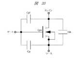
このようなパワーMISFETは、たとえばデスクトップ、ノートおよびサーバなどの各種コンピュータの電源回路に用いられるDC/DCコンバータのスイッチング素子として用いられる。このようなDC/DCコンバータには、チョークコイルおよび入出力などの容量の小型化や、負荷変動に対する高速応答の要求がある。そのため、DC/DCコンバータのシステムとしては高周波化の傾向があり、そのシステムの高周波化に伴ってパワーMISFETにおいては、スイッチング損失およびドライブ損失が増加する。スイッチング損失はパワーMISFETの帰還容量に比例し、ドライブ損失はパワーMISFETの入力容量に比例することから、DC/DCコンバータに用いられるパワーMISFETには、これらの容量の低減が求められる。ここで、図33は、その帰還容量および入力容量を説明する等価回路図である。図33に示すように、Cgdをゲート−ドレイン間容量とし、Cgsをゲート−ソース間容量とし、Cdsをドレイン−ソース間容量とすると、パワーMISFETQpwの入力容量Cinは、Cin≒Cgd+Cgsと表すことができ、帰還容量Cfbは、Cfb=Cgdと表すことができる。また、図34は、そのゲート−ソース間容量およびゲート−ドレイン間容量を説明する要部断面図である。図34に示すように、ゲート電極GELE、ソースであるn+型半導体領域NSEMおよびドレインであるn-型単結晶シリコン層NEPIに印加される電圧を、それぞれVG、VSおよびVDとし、チャネルであるp-型半導体領域PBODにもソースと同電位の電圧VSが印加されるものとする。この条件下において、たとえば電圧VG、VSを0Vとし、電圧VDを周波数1MHzで0Vから10Vまでの変化する電圧とすると、ゲート−ソース間容量は、ゲート電極GELEおよびp-型半導体領域PBODを容量電極としゲート絶縁膜GINSを容量絶縁層とする容量C1と、ゲート電極GELEおよびp-型半導体領域PBODを容量電極とし空乏層DEP(図34で灰色の着色を施してある領域)を容量絶縁層とする容量C2とを直列接続したものとして表すことができ、ゲート−ドレイン間容量は、ゲート電極GELEおよびn-型単結晶シリコン層NEPIを容量電極としゲート絶縁膜GINSを容量絶縁層とする容量C3と、ゲート電極GELEおよびn-型単結晶シリコン層NEPIを容量電極とし空乏層DEPを容量絶縁層とする容量C4とを直列接続したものとして表すことができる。Such power MISFETs are used as switching elements of DC / DC converters used in power supply circuits of various computers such as desktops, notebooks, and servers. Such a DC / DC converter is required to have a smaller capacity such as a choke coil and an input / output and a high-speed response to a load change. For this reason, the DC / DC converter system tends to have a higher frequency, and the switching loss and the drive loss increase in the power MISFET as the frequency of the system increases. Since the switching loss is proportional to the feedback capacitance of the power MISFET and the drive loss is proportional to the input capacitance of the power MISFET, the power MISFET used in the DC / DC converter is required to reduce these capacitances. Here, FIG. 33 is an equivalent circuit diagram for explaining the feedback capacitance and the input capacitance. As shown in FIG. 33, when Cgd is a gate-drain capacitance, Cgs is a gate-source capacitance, and Cds is a drain-source capacitance, the input capacitance Cin of the power MISFET Qpw can be expressed as Cin≈Cgd + Cgs. The feedback capacitance Cfb can be expressed as Cfb = Cgd. FIG. 34 is a cross-sectional view of the main part for explaining the gate-source capacitance and the gate-drain capacitance. As shown in FIG. 34, the voltages applied to the gate electrode GELE, the n+ type semiconductor region NSEM as the source, and the n− type single crystal silicon layer NEPI as the drain are VG, VS, and VD, respectively, which are the channels. It is assumed that the voltage VS having the same potential as the source is also applied to the p− type semiconductor region PBOD. Under these conditions, for example, assuming that the voltages VG and VS are 0 V and the voltage VD is a voltage that changes from 0 V to 10 V at a frequency of 1 MHz, the gate-source capacitance is the capacitance of the gate electrode GELE and the p− type semiconductor region PBOD. The capacitor C1 having the electrode and the gate insulating film GINS as the capacitor insulating layer, and the depletion layer DEP (the region colored in gray in FIG. 34) having the gate electrode GELE and the p− type semiconductor region PBOD as the capacitor electrode The capacitance between the gate and the drain is a capacitance in which the gate electrode GELE and the n− type single crystal silicon layer NEPI are used as a capacitance electrode and the gate insulating film GINS is used as a capacitance insulating layer. and C3, the gate electrode GELE and the n- depletion DEP and type single crystal silicon layer NEPI capacitance electrode capacitance And a capacitor C4 to the edge layer can be represented as connected in series.
また、近年、上記DC/DCコンバータが電力を供給するCPU(Central Processing Unit)等には大電流化の傾向があるため、DC/DCコンバータにも大電流化が求められている。そのため、パワーMISFETにおけるオン損失の増加が懸念される。従って、DC/DCコンバータに用いられるパワーMISFETには、低オン抵抗化も求められる。 Further, in recent years, since there is a tendency to increase current in a CPU (Central Processing Unit) or the like to which power is supplied by the DC / DC converter, the DC / DC converter is also required to increase current. Therefore, there is a concern about an increase in on-loss in the power MISFET. Therefore, the power MISFET used in the DC / DC converter is also required to have a low on-resistance.
上記トレンチゲート型パワーMISFETは、半導体基板(以下、単に基板という)の主面(素子形成面)に深い溝を形成し、その溝に導電体を埋め込むことでゲート部が形成される。また、プレーナゲート型パワーMISFETは、基板の主面上にゲート絶縁膜を介してゲート部が形成される。そのため、トレンチゲート型パワーMISFETは、プレーナゲート型パワーMISFETに比べて基板内における電流の流れる経路が短くなるので、オン抵抗を小さくすることができる。しかしながら、ゲート絶縁膜が溝の側壁および底面に形成されるので、溝が深くなることによって、そのゲート絶縁膜を容量絶縁膜としゲート部を容量電極とする容量成分が増加してしまう課題が存在する。一方、プレーナゲート型パワーMISFETは、トレンチゲート型パワーMISFETに比べてゲート絶縁膜を容量絶縁膜としゲート部を容量電極とする容量成分を小さくできる反面、ピンチオフの発生を防ぐために十分なゲート長を確保しようとすると、単位面積当たりで配置できるゲート部の数が少なくなる。そのため、パワーMISFETが形成される半導体チップの面積を一定とすれば、プレーナゲート型パワーMISFETの場合には半導体チップ内に配置できるゲート部の数がトレンチゲート型パワーMISFETに比べて少なくなる。その結果、プレーナゲート型パワーMISFETは、半導体チップ全体ではトレンチゲート型パワーMISFETに比べてオン抵抗が増加してしまう課題が存在する。また、プレーナゲート型パワーMISFETは、トレンチゲート型パワーMISFETに比べて基板内における電流の流れる経路が長くなるので、オン抵抗が増加してしまう課題が存在する。すなわち、DC/DCコンバータの高周波化および大電流化を考慮した場合、パワーMISFETに求められる低オン抵抗化および低容量化を同時に満たすことが困難になる課題が存在する。 In the trench gate type power MISFET, a deep groove is formed in a main surface (element formation surface) of a semiconductor substrate (hereinafter simply referred to as a substrate), and a gate is formed by embedding a conductor in the groove. In the planar gate type MISFET, a gate portion is formed on the main surface of the substrate via a gate insulating film. Therefore, the trench gate type power MISFET has a shorter path for current flow in the substrate than the planar gate type power MISFET, so that the on-resistance can be reduced. However, since the gate insulating film is formed on the side wall and the bottom surface of the groove, there is a problem that when the groove becomes deep, a capacity component having the gate insulating film as a capacitive insulating film and the gate portion as a capacitive electrode increases. To do. On the other hand, the planar gate type power MISFET can reduce the capacitance component in which the gate insulating film is a capacitive insulating film and the gate portion is a capacitive electrode, but has a sufficient gate length to prevent pinch-off compared to the trench gate type power MISFET. If it is going to be secured, the number of gate portions that can be arranged per unit area is reduced. Therefore, if the area of the semiconductor chip on which the power MISFET is formed is constant, in the case of the planar gate type power MISFET, the number of gate portions that can be arranged in the semiconductor chip is smaller than that of the trench gate type power MISFET. As a result, the planar gate type power MISFET has a problem that the on-resistance increases in the entire semiconductor chip as compared with the trench gate type power MISFET. In addition, the planar gate type power MISFET has a problem in that the on-resistance increases because a path through which current flows in the substrate becomes longer than the trench gate type power MISFET. That is, when considering the high frequency and large current of the DC / DC converter, there is a problem that it is difficult to simultaneously satisfy the low on-resistance and low capacitance required for the power MISFET.
そこで、本発明者らは、トレンチゲート型パワーMISFETを低容量化する技術について検討している。図35は、本発明者らが検討したトレンチゲート型パワーMISFETの要部断面図である。図35に示すトレンチゲート型パワーMISFETは、n+型単結晶シリコン基板101およびその上部に形成されたn-型単結晶シリコン層102からなる基板の主面に溝103が形成され、この溝103内にゲート絶縁膜104を介して導電体が埋め込まれることでゲート部105が形成されたトレンチゲート構造となっている。このようなトレンチゲート構造とした場合、相対的に不純物濃度の低いn-型単結晶シリコン層102内での電流の流れる経路をプレーナゲート構造とした場合より短くできるので、オン抵抗となるJFET(Junction FET)抵抗成分を小さくすることができる。また、ソース電極106は、基板の主面および絶縁膜107に形成された溝108内を埋め込むように形成され、チャネル層となるp-型半導体領域109内に形成されたp+型半導体領域110およびソース領域となるn+型半導体領域111と電気的に接続している。p+型半導体領域110は、溝108から基板へ不純物イオンを自己整合的に導入することで形成することができるので、不純物イオン導入のためのマスク合わせ余裕を考慮しなくてもよくなる。そのため、MISFETのセルピッチを縮小できるので、MISFETを高集積化してさらにオン抵抗を低減することができる。また、トレンチゲート構造としたことにより、チャネル長が基板の深さ方向となることから、チャネル長が基板の主面に沿った方向となるプレーナゲート構造に比べてMISFETのセルピッチを縮小することができる。Therefore, the present inventors are examining a technique for reducing the capacitance of the trench gate type power MISFET. FIG. 35 is a fragmentary cross-sectional view of a trench gate type power MISFET studied by the present inventors. In the trench gate type power MISFET shown in FIG. 35, a
しかしながら、ゲート部105が形成された溝103は、深さが、たとえば約1μm以上と深く形成されていることから、前述のゲート絶縁膜を容量絶縁膜としゲート部を容量電極とする容量成分を低減することが困難になっている。この容量成分のうち、前述の入力容量は溝103の周囲の長さ(n+型半導体領域111下の溝103の表面積)に比例し、帰還容量は溝103のp-型半導体領域109からn-型単結晶シリコン層102へのはみ出し距離(n-型単結晶シリコン層102と接する溝103の表面積)D12に比例する。そのため、入力容量を低減するためには溝103を狭幅化する手段が考えられ、帰還容量を低減するためにはp-型半導体領域109からn-型単結晶シリコン層102へのはみ出し距離D12を小さく(浅溝化)する手段が考えられる。ところが、溝103を狭幅化するには、加工寸法の限界があることと、溝103の幅が狭くなり過ぎるとゲート部105の抵抗の増大を招いてしまう課題が存在する。また、溝103を浅溝化するためには、それに合わせてp-型半導体領域109とn-型単結晶シリコン層102との接合部も浅い位置に設定(浅接合化)しなければならない。このように浅接合化した場合には、ドレイン・ソース間に電圧を印加した際にチャネル層(p-型半導体領域109)が空乏化し、パンチスルーを起こしてしまうという課題が存在する。ここで、上記特許文献1および特許文献2には、浅溝化によって容量成分を低減する技術は開示されておらず、浅溝化によって発生するパンチスルーの問題についても開示されていない。このようなチャネル層の空乏化を防ぐために、p-型半導体領域109の不純物濃度を高くすると、MISFETのしきい値電圧が上がり、オン抵抗が高くなってしまうという課題が存在する。このような狭幅化および浅溝化によって発生する課題について、上記特許文献1および特許文献2に記載された技術では考慮がなされていない。また、p-型半導体領域109からn-型単結晶シリコン層102へのはみ出し距離を小さくするために、p-型半導体領域109の深さを溝103の深さと同じとなるように設計すると、溝103の製造上のばらつきによって、p-型半導体領域109が溝103の底部を覆ってしまう箇所が生じ、MISFETのしきい値電圧が上がり、オン抵抗が高くなってしまうという課題が発生する。However, since the
本発明の目的は、トレンチゲート型パワーMISFETの低オン抵抗化および低容量化を同時に実現できる技術を提供することにある。 An object of the present invention is to provide a technique capable of simultaneously realizing low ON resistance and low capacitance of a trench gate type power MISFET.
本発明の前記ならびにその他の目的と新規な特徴は、本明細書の記述および添付図面から明らかになるであろう。 The above and other objects and novel features of the present invention will be apparent from the description of this specification and the accompanying drawings.
本願において開示される発明のうち、代表的なものの概要を簡単に説明すれば、次のとおりである。 Of the inventions disclosed in the present application, the outline of typical ones will be briefly described as follows.
本発明による半導体装置は、
MISFETを有し、
半導体基板の主面に形成された第1導電型の第1半導体層と、
前記第1半導体層上に形成され、前記第1導電型とは逆の第2導電型の第2半導体層と、
前記半導体基板の主面に形成され、少なくとも底部の一部が前記第1半導体層と接し、深さが1μm以下である複数の第1溝部と、
前記第1溝部の側壁および底面に形成された第1絶縁膜と、
前記第1絶縁膜上に形成され、前記第1溝部を埋め込む第1導電体と、
前記第1溝部に隣接して前記第2半導体層内に形成され、前記第1導電型を有する第3半導体層と、
隣り合う前記第1溝部間の前記第2半導体層内に形成された前記第2導電型の第4半導体層と、
前記第3半導体層および前記第4半導体層と電気的に接続する第1電極とを有し、
前記第1半導体層および前記第3半導体層は、前記MISFETのソースまたはドレインを形成し、前記第2半導体層は、前記MISFETのチャネル形成領域を形成し、
前記第2半導体層内の前記第3半導体層の下部に前記第2半導体層より不純物濃度が高い前記第2導電型の第5半導体層が形成されている。A semiconductor device according to the present invention includes:
Having a MISFET,
A first semiconductor layer of a first conductivity type formed on the main surface of the semiconductor substrate;
A second semiconductor layer formed on the first semiconductor layer and having a second conductivity type opposite to the first conductivity type;
A plurality of first grooves formed on the main surface of the semiconductor substrate, at least part of which is in contact with the first semiconductor layer and having a depth of 1 μm or less;
A first insulating film formed on a side wall and a bottom surface of the first groove,
A first conductor formed on the first insulating film and burying the first groove;
A third semiconductor layer formed in the second semiconductor layer adjacent to the first groove and having the first conductivity type;
A second semiconductor layer of the second conductivity type formed in the second semiconductor layer between the adjacent first groove portions;
A first electrode electrically connected to the third semiconductor layer and the fourth semiconductor layer;
The first semiconductor layer and the third semiconductor layer form a source or drain of the MISFET, the second semiconductor layer forms a channel formation region of the MISFET,
A fifth semiconductor layer of the second conductivity type having an impurity concentration higher than that of the second semiconductor layer is formed below the third semiconductor layer in the second semiconductor layer.
また、本発明による半導体装置の製造方法は、MISFETを有する半導体装置の製造方法であって、
(a)半導体基板の主面に第1導電型の第1半導体層を形成する工程と、
(b)前記半導体基板に前記第1導電型とは逆の第2導電型の不純物を導入して、前記第1半導体層上に前記第2導電型の第2半導体層を形成する工程と、
(c)前記半導体基板の主面に複数の第1溝部を形成する工程と、
(d)前記第1溝部内に第1絶縁膜を形成する工程と、
(e)前記第1絶縁膜の存在下で前記第1溝部内に第1導電体を埋め込み、ゲート電極を形成する工程と、
(f)前記半導体基板に前記第1導電型の不純物を導入して、前記第2半導体層上に前記第1溝部と隣接する前記第1導電型の第3半導体層を形成する工程と、
(g)前記半導体基板に前記第1導電型とは逆の前記第2導電型の不純物を導入して、前記第2半導体層内の前記第3半導体層の下部に前記第2導電型の第5半導体層を形成する工程と、
(h)隣り合う前記ゲート電極間に配置されるように、前記半導体基板の主面に前記第3半導体層を貫通する複数の第2溝部を形成する工程と、
(i)前記第2溝部の底部から前記半導体基板に前記第2導電型の不純物を導入し、前記第2半導体層内にて前記第2溝部の底部を覆うように前記第2導電型の第4半導体層を形成する工程と、
(j)前記第2溝部を埋め込み、前記第3半導体層および前記第4半導体層と電気的に接続する第1電極を形成する工程とを含み、
前記第1溝部は、少なくとも底部の一部が前記第1半導体層と接し、深さが1μm以下となるように形成し、
前記第5半導体層は、前記第2半導体層より不純物濃度が高くなるように形成し、
前記第1半導体層および前記第3半導体層が前記MISFETのソースまたはドレインとなり、前記第2半導体層が前記MISFETのチャネル形成領域となる前記MISFETを形成するものである。A method for manufacturing a semiconductor device according to the present invention is a method for manufacturing a semiconductor device having a MISFET,
(A) forming a first conductivity type first semiconductor layer on a main surface of a semiconductor substrate;
(B) introducing a second conductivity type impurity opposite to the first conductivity type into the semiconductor substrate to form the second conductivity type second semiconductor layer on the first semiconductor layer;
(C) forming a plurality of first grooves on the main surface of the semiconductor substrate;
(D) forming a first insulating film in the first groove portion;
(E) burying a first conductor in the first trench in the presence of the first insulating film to form a gate electrode;
(F) introducing the first conductivity type impurity into the semiconductor substrate to form the first conductivity type third semiconductor layer adjacent to the first groove on the second semiconductor layer;
(G) An impurity of the second conductivity type opposite to the first conductivity type is introduced into the semiconductor substrate, and the second conductivity type second impurity is formed below the third semiconductor layer in the second semiconductor layer. 5 forming a semiconductor layer;
(H) forming a plurality of second grooves penetrating the third semiconductor layer in the main surface of the semiconductor substrate so as to be disposed between the adjacent gate electrodes;
(I) Impurities of the second conductivity type are introduced into the semiconductor substrate from the bottom of the second groove portion, and the second conductivity type second so as to cover the bottom portion of the second groove portion in the second semiconductor layer. 4 forming a semiconductor layer;
(J) filling the second groove portion and forming a first electrode electrically connected to the third semiconductor layer and the fourth semiconductor layer,
The first groove is formed such that at least a part of the bottom is in contact with the first semiconductor layer and the depth is 1 μm or less.
The fifth semiconductor layer is formed to have a higher impurity concentration than the second semiconductor layer,
The first semiconductor layer and the third semiconductor layer form a source or drain of the MISFET, and the second semiconductor layer forms the MISFET that forms a channel formation region of the MISFET.
本願において開示される発明のうち、代表的なものによって得られる効果を簡単に説明すれば以下のとおりである。 Among the inventions disclosed in the present application, effects obtained by typical ones will be briefly described as follows.
すなわち、トレンチゲート型パワーMISFETの低オン抵抗化および低容量化を同時に実現できる。 That is, the on-resistance and the capacitance of the trench gate type power MISFET can be simultaneously realized.
以下、本発明の実施の形態を図面に基づいて詳細に説明する。なお、実施の形態を説明するための全図において、同一の部材には原則として同一の符号を付し、その繰り返しの説明は省略する。また、以下の実施の形態を説明する図面においては、構成をわかりやすくするために平面図であってもハッチングを付す場合がある。 Hereinafter, embodiments of the present invention will be described in detail with reference to the drawings. Note that components having the same function are denoted by the same reference symbols throughout the drawings for describing the embodiment, and the repetitive description thereof will be omitted. Further, in the drawings for explaining the following embodiments, hatching may be given even in plan views for easy understanding of the configuration.
(実施の形態1)
本実施の形態1の半導体装置は、たとえばnチャネル型のトレンチゲート型パワーMISFETを有するものである。このような本実施の形態1の半導体装置について図1〜図25を用いて製造工程に従って説明する。(Embodiment 1)
The semiconductor device of the first embodiment has, for example, an n-channel trench gate type power MISFET. Such a semiconductor device according to the first embodiment will be described according to the manufacturing process with reference to FIGS.
まず、図1に示すように、n型(第1導電型)の導電型を有するn+型単結晶シリコン基板1Aの表面(主面)に、n型の導電型を有する不純物(たとえば、P(リン))がドープされたn-型単結晶シリコン層(第1半導体層)1Bをエピタキシャル成長させた半導体基板(以下、単に基板という)1を準備する。本実施の形態1においては、基板1として、(100)面を主面(素子形成面)とする半導体ウエハ(以下、第1のウエハという)を基準として、その主面の法線から第1のウエハに形成されたオリエンテーションフラットまたはノッチの方向に所定の角度だけ傾いた直線を法線とする面を主面とするウエハ(以下、第2のウエハという)から形成された、いわゆるオフアングル基板を用いる。また、n+型単結晶シリコン基板1Aおよびn-型単結晶シリコン層1Bは、後の工程でパワーMISFETのドレイン領域となる。First, as shown in FIG. 1, an impurity (for example, P) is formed on the surface (main surface) of an n+ type single
次に、図2に示すように、たとえばn-型単結晶シリコン層1Bの表面(主面)を熱酸化することによって酸化シリコン膜3を形成する。次いで、酸化シリコン膜3上に、フォトリソグラフィ技術を用いてパターニングされた窒化シリコン膜(図示は省略)等をマスクとして、p型の導電型を有する不純物(たとえばB(ホウ素))を注入し、熱拡散させることによりp型ウエル5を形成する。その後、前記窒化シリコン膜を除去する。Next, as shown in FIG. 2, the
次に、図3に示すように、フォトリソグラフィ技術によってパターニングされたフォトレジスト膜をマスクとして酸化シリコン膜3および基板1をエッチングし、溝7(第1溝部)を形成する。本実施の形態1において、溝7は、深さ約1μm以下で浅く形成する。また、平面において、この溝7は、四角形、六角形または八角形などの形で延在するメッシュ状のパターンや、同一方向に多数本延在するストライプ状パターンとする。続いて、基板1に熱処理を施すことにより、溝7の底部および側壁に熱酸化膜(第1絶縁膜)9を形成する。この熱酸化膜9は、パワーMISFETのゲート絶縁膜となる。 Next, as shown in FIG. 3, the
次に、図4に示すように、たとえばPがドープされた多結晶シリコン膜を溝7の内部を含む酸化シリコン膜3上に堆積し、その多結晶シリコン膜で溝7を埋め込む。この時、p型ウエル5上の酸化シリコン膜3上には、多結晶シリコン膜が層状に形成される。続いて、フォトリソグラフィ技術によりパターニングされたフォトレジスト膜をマスクとしてその多結晶シリコン膜をエッチングし、多結晶シリコン膜を溝7内に残すことによって、溝7内にパワーMISFETのゲート電極(第1導電体)10を形成する。また、この時、チップ領域(図示は省略)の外周部の酸化シリコン膜3上にも多結晶シリコン膜を残し、多結晶シリコンパターン11を形成する。ゲート電極10と多結晶シリコンパターン11とは、図4に示されない領域において電気的に接続されている。 Next, as shown in FIG. 4, for example, a polycrystalline silicon film doped with P is deposited on the
続いて、フォトリソグラフィ技術によりパターニングされたフォトレジスト膜をマスクとして酸化シリコン膜3をエッチングし、不要な酸化シリコン膜3を除去する。それにより、多結晶シリコン膜パターン11の下部の酸化シリコン膜3の形成領域は素子分離領域となり、この領域で区画される領域が素子形成領域(アクティブ)となる。 Subsequently, the
次に、図5に示すように、基板1上に酸化シリコン膜12を堆積する。続いて、図6に示すように、フォトリソグラフィ技術によりパターニングされたフォトレジスト膜をマスクとしてp型(第2導電型)の導電型を有する不純物イオン(たとえばB(ホウ素))を5×10¹²個/cm2程度の濃度でn-型単結晶シリコン層1Bに導入する。次いで、基板1に熱処理を施すことによってその不純物イオンを拡散させ、p-型半導体領域(第2半導体層)13を形成する。この時、p-型半導体領域13は、溝7の底部を覆わないように形成する。このp-型半導体領域13は、パワーMISFET形成後においてパワーMISFETのチャネル層となる。また、本実施の形態1において、p-型半導体領域13は、溝7より約10%以上浅くなるように設計する。すなわち、前述したように、溝7は、約10μm以下の深さで設計(形成)しているので、溝7のp-型半導体領域13からのはみだし量を約0.1μm以下の深さにできる。Next, as shown in FIG. 5, a
続いて、フォトリソグラフィ技術によってパターニングされたフォトレジスト膜をマスクとしてp型の導電型を有する不純物イオン(たとえばB)を3×1012個/cm2程度の濃度でn-型単結晶シリコン層1Bに導入することによって、上記p-型半導体領域13より不純物濃度の高いp型半導体領域(第5半導体層)14を形成する。この時、そのフォトレジスト膜のパターニングに用いるフォトマスクとしては、上記p-型半導体領域13を形成時におけるフォトレジスト膜のパターニングに用いたフォトマスクを再度用いることを例示できる。それにより、p型半導体領域14を形成する工程に用いる新たなフォトマスクを製作する必要がなくなるので、本実施の形態1の半導体装置の製造コストを低減することができる。続いて、フォトリソグラフィ技術によってパターニングされたフォトレジスト膜をマスクとしてn型の導電型を有する不純物イオン(たとえばAs(ヒ素))をn-型単結晶シリコン層1Bに導入する。続いて、基板1に熱処理を施すことによってその不純物イオンを拡散させ、p-型半導体領域13内においてp型半導体領域14上にn+型半導体領域(第3半導体層)15を形成する。ここまでの工程により、n+型単結晶シリコン基板1Aおよびn-型単結晶シリコン層1Bをドレイン領域とし、n+型半導体領域15をソース領域とするパワーMISFETを形成することができる。また、p型半導体領域14は、本実施の形態1のパワーMISFETにおけるパンチスルーストッパー層とすることができる。Subsequently, the n− type single
次に、図7に示すように、たとえば基板上にPSG(Phospho Silicate Glass)膜を堆積した後、そのPSG膜上にSOG(Spin On Glass)膜を塗布することにより、そのPSG膜およびSOG膜からなる絶縁膜16を形成する。続いて、フォトリソグラフィ技術によってパターニングされたフォトレジスト膜をマスクとして絶縁膜16、酸化シリコン膜12および基板1をエッチングし、コンタクト溝(第2溝部)17を形成する。コンタクト溝17は、隣接するゲート電極10間において、パワーMISFETのソース領域となるn+型半導体領域15を貫通するように形成される。また、この時、多結晶シリコンパターン11上の絶縁膜16および酸化シリコン膜12もパターニングされ、多結晶シリコンパターン11に達するコンタクト溝18が形成される。Next, as shown in FIG. 7, for example, a PSG (Phospho Silicate Glass) film is deposited on a substrate, and then an SOG (Spin On Glass) film is applied on the PSG film to thereby form the PSG film and the SOG film. An insulating
次に、図8に示すように、コンタクト溝17の底部からp型の導電型を有する不純物イオンとして、たとえばBF2(二フッ化ホウ素)を導入することによって、コンタクト溝17の底部を覆うようなp+型半導体領域(第4半導体層)20を形成する。本実施の形態1において、このp+型半導体領域20中の不純物濃度は、p型半導体領域14中の不純物濃度より高くなるようにする。このように、コンタクト溝17を形成し、絶縁膜16をマスクとしてコンタクト溝17から不純物イオンを導入し、コンタクト溝17の底部に自己整合的にp+型半導体領域20を設けることによって、たとえばマスク合わせ余裕を低減できるので、隣接するゲート電極10間の微細化を図ることができる。このp+型半導体領域20は、後の工程で形成される配線をコンタクト溝17の底部にてp-型半導体領域13とオーミック接触させるためのものである。Next, as shown in FIG. 8, BF2 (boron difluoride), for example, is introduced as impurity ions having p-type conductivity from the bottom of the
次に、図9〜図11に示すように、コンタクト溝17、18の内部を含む絶縁膜16の上部に、バリア導体膜として、たとえばスパッタリング法でTiW(チタンタングステン)膜を薄く堆積した後、基板1に熱処理を施す。続いて、そのTiW膜上に、たとえばスパッタリング法にてゲート電極10を形成する多結晶シリコン膜より抵抗率の低いAl(アルミニウム)膜(第2導電体)を堆積する。バリア導体膜は、Alと基板(Si)とが接触することにより不所望な反応層が形成されることを防止する役割を果たす。なお、本実施の形態1において、Al膜は、Alを主成分とする膜を意味し、他の金属等を含有していてもよい。 Next, as shown in FIGS. 9 to 11, after a thin TiW (titanium tungsten) film is deposited as a barrier conductor film on the insulating
続いて、フォトリソグラフィ技術によりパターニングされたフォトレジスト膜をマスクとしてそのTiW膜およびAl膜をエッチングすることにより、ゲート電極10と電気的に接続するゲート配線(第2電極、第1部)21、パワーMISFETのソース領域となるn+型半導体領域15と電気的に接続するソースパッド(第1電極)22、ゲート配線21と電気的に接続するゲートパッドGP、ソースパッド22と電気的に接続する配線L1、および配線L2、L3を形成する。ここで、図10および図11は、後の工程で基板1を個々のチップへ分割した時のチップ1個分に相当するチップ領域CHPを示したものであり、図10ではゲート電極10が平面で四角形のメッシュ状に形成された場合を図示し、図11ではゲート電極10が平面でストライプ状に形成された場合を図示している。Subsequently, a gate wiring (second electrode, first part) 21 electrically connected to the
ここで、図12は、ゲート電極10付近を拡大して示した要部断面図である。また、図13は、図12中のA−A線に沿った位置における、基板1の表面からの深さと不純物濃度との関係を示したものである。 Here, FIG. 12 is an enlarged cross-sectional view showing the vicinity of the
前述したように、本実施の形態1では、溝7は、深さD1が約1μm以下と浅く形成されている。すなわち、溝7の浅溝化によって、ゲート絶縁膜(熱酸化膜9)を容量絶縁膜としゲート電極10を容量電極とする容量成分のうち、入力容量を低減することができる。また、本実施の形態1において、ゲート電極10を容量電極としゲート絶縁膜(熱酸化膜9)を容量絶縁膜とするゲート容量は、ゲート電極10およびソース領域(n+型半導体領域15)に0Vの電圧を印加し、ドレイン領域(n+型単結晶シリコン基板1Aおよびn-型単結晶シリコン層1B)に周波数1MHzで0Vから10Vまでの変化する電圧を印加した状態において、平面でゲート電極10(溝7)の延在する方向における1μm当たりで1×10⁻³pF程度以下とすることができる。たとえば、図11に示したように、ゲート電極10(溝7)が平面でストライプ状のパターンで形成されている場合には、紙面の左右方向をX方向とし上下方向をY方向とすれば、平面でゲート電極10(溝7)の延在する方向(第1方向)はY方向で規定できる。As described above, in the first embodiment, the
ここで、溝7の浅溝化に合わせてp-型半導体領域13も浅く形成し、p-型半導体領域13とn-型単結晶シリコン層1Bとの接合部も浅い位置に設定(浅接合化)しなければならないが、このように浅接合化した場合には、ドレイン・ソース間に電圧を印加した際にパワーMISFETのチャネル層(p-型半導体領域13)が空乏化し、パンチスルーの発生が懸念される。このようなチャネル層の空乏化を防ぐために、p-型半導体領域13の不純物濃度を高くすると、パワーMISFETのしきい値電圧が上がり、オン抵抗が高くなってしまうことが懸念される。そこで本実施の形態1では、p-型半導体領域13の不純物濃度を高くせずに、p-型半導体領域13中に局所的にp-型半導体領域13より不純物濃度の高いp型半導体領域14を形成し、このp型半導体領域14をパンチスルーストッパー層としている。それにより、本実施の形態1のパワーMISFETにおいては、しきい値電圧の上昇およびオン抵抗の増大を防ぎつつ、パンチスルーの発生を防ぐことが可能となる。すなわち、本実施の形態1のパワーMISFETによれば、パンチスルーの発生を防ぎつつ、入力容量の低減を実現することができる。しきい値電圧については、約2V以下とすることができる。また、本実施の形態1におけるp-型半導体領域13形成のための不純物導入量とp型半導体領域14形成のための不純物導入量との合計値は、溝7の深さが約1μm以上でありパンチスルーストッパー層(p型半導体領域14)を有していないパワーMISFET(以降、本発明者らが検討した第1のパワーMISFETという)におけるp-型半導体領域13形成のための不純物導入量と同程度となるようにする。それにより、本実施の形態1のパワーMISFETにおいては、本発明者らが検討した第1のパワーMISFETに比べて、p-型半導体領域13形成のための不純物導入量が少なくなる。また、本発明者らが検討した第1のパワーMISFETに比べて、溝7の深さが浅くなるので、p-型半導体領域13を溝7の底部を覆わないように形成し、かつp-型半導体領域13とn-型単結晶シリコン層1Bとの浅接合化を実現するために、p-型半導体領域13形成のための不純物導入後における熱処理は、本発明者らが検討した第1のパワーMISFETの製造工程に比べて、処理温度を低温化し、処理時間を短縮化することが好ましい。また、パンチスルーストッパー層となるp型半導体領域14は、p-型半導体領域13形成のための熱処理後に形成することが好ましい。それにより、p型半導体領域14形成のための不純物導入後に基板1に施される熱処理時間を短縮化することができるので、p型半導体領域14をp-型半導体領域13中に局所的に形成することが可能となる。また、本実施の形態1のパワーMISFETのソース領域となるn+型半導体領域15についても、浅く形成するために、n+型半導体領域15形成のための不純物導入後における熱処理は極力処理時間を短くすることが好ましく、たとえばランプアニール処理などの熱処理時間の短い手段を適用することが好ましい。Here, the p−
また、溝7の深さを浅くすることにより、その深さの製造上のばらつきを小さくすることができるので、溝7のp-型半導体領域13からn-型単結晶シリコン層1Bへのはみ出し距離D2を小さくすることができる。すなわち、ゲート絶縁膜(熱酸化膜9)を容量絶縁膜としゲート電極10を容量電極とする容量成分のうち、帰還容量は溝7のp-型半導体領域13からn-型単結晶シリコン層1Bへのはみ出し距離に比例することから、溝7のp-型半導体領域13からn-型単結晶シリコン層1Bへのはみ出し距離が小さくなることによって、その帰還容量を低減することができる。p-型半導体領域13については、p-型半導体領域13が溝7の底部を覆ってしまわないように、たとえば溝7の深さより約10%以上浅く形成されるように設計される。そのため、溝7の深さが約1μm以上であれば、溝7のp-型半導体領域13からn-型単結晶シリコン層1Bへのはみ出し距離D2は、約0.1μm以下にはできないということになる。一方、本実施の形態1によれば、溝7の深さは約1μm以下とするので、溝7のp-型半導体領域13からn-型単結晶シリコン層1Bへのはみ出し距離D2を約0.1μm以下にすることができる。それにより、本実施の形態1のパワーMISFETによれば、本発明者らが検討した第1のパワーMISFETに比べて、帰還容量を低減することができる。Further, since the manufacturing variation of the depth can be reduced by reducing the depth of the
また、上記のp型半導体領域14を形成することによって、n-型単結晶シリコン層1Bをコレクタとし、p-型半導体領域13をベースとし、n+型半導体領域15をエミッタとする寄生npn型バイポーラトランジスタのベース抵抗を低減することができる。それにより、本実施の形態1のパワーMISFETのアバランシェ耐量を向上することができる。Further, by forming the p-
本発明者らは、上記パンチスルーストッパー層となるp型半導体領域14を設けていない場合における、チャネル層であるp-型半導体領域13にてパンチスルーの発生状況を実験により調べた。図14は、p型半導体領域14を設けた場合と設けていない場合とのそれぞれにおける、パワーMISFETのソース・ドレイン間電圧Vdsとドレイン電流Idとの関係を示したものである。図14に示すように、p型半導体領域14を設けていない場合には、p-型半導体領域13にてパンチスルーが発生し、設けている場合に比べてリーク電流成分が大きくなっていることがわかる。すなわち、p型半導体領域14を設けたことによって、本実施の形態1のようにp-型半導体領域13とn-型単結晶シリコン層1Bとの接合部を浅い位置に設定(浅接合化)した場合でも、ドレイン・ソース間に電圧を印加した際にチャネル層(p-型半導体領域13)が空乏化し、パンチスルーを起こしてしまう不具合を防ぐことができる。The inventors examined the occurrence of punch-through in the p− -
上記の本実施の形態1のパワーMISFETは、たとえば図15に示すようなDC/DCコンバータの回路中におけるスイッチング素子(High−sideMISFETQHおよびLow−sideMISFETQL)として用いられる。本発明者らは、このようなDC/DCコンバータの全損失の成分分析をシミュレーションによって行い、その成分の内訳について調べた。シミュレーション条件としては、入力電圧Vinを12V、出力電圧Voutを1.3V、および回路の動作周波数を1MHzとし、出力電流Ioutが2Aおよび10Aのそれぞれの場合について調べた。図16および図17は、それぞれ出力電流Ioutが2Aおよび10Aの時のDC/DCコンバータの全損失の成分の内訳を示すものである。図16および図17に示すように、DC/DCコンバータの全損失のうち、スイッチング損失とドライブ損失との合計は、出力電流Ioutが2Aの時で約56%を占め、出力電流Ioutが10Aの時で約41%を占めている。ここでスイッチング損失とは、パワーMISFETがONまたはOFFする時に発生する損失であり、ドライブ損失とはパワーMISFETのゲートを駆動するのに必要となる電力のことをいう。また、パワーMISFETのドレイン・ソース間電圧をVdsとし、ドレイン電流をIdとし、trをオン時間とし、tfをオフ時間とし、Qgを入力ゲート容量とし、Vgsをゲート・ソース間電圧とし、fを回路の動作周波数とすると、スイッチング損失は1/2×(tr+tf)×Id×Vds×fと表すことができ、ドライブ損失はQg×Vgs×fと表すことができる。これらの式より、スイッチング損失およびドライブ損失は、周波数に比例するので、回路の高周波化に伴ってこれらスイッチング損失およびドライブ損失も増大することになる。また、スイッチング損失はパワーMISFETの帰還容量に比例し、ドライブ損失はパワーMISFETの入力容量に比例する。前述したように、本実施の形態1によれば、パワーMISFETの帰還容量および入力容量を低減できるので、DC/DCコンバータの損失を大幅に低減することができる。それにより、DC/DCコンバータシステムの高効率化を実現することができる。The power MISFET of the first embodiment is used as a switching element (High-side MISFET QH and Low-side MISFET QL ) in a DC / DC converter circuit as shown in FIG. 15, for example. The present inventors conducted a component analysis of the total loss of such a DC / DC converter by simulation and examined the breakdown of the components. As simulation conditions, the input voltage Vin was 12 V, the output voltage Vout was 1.3 V, the circuit operating frequency was 1 MHz, and the output current Iout was 2 A and 10 A, respectively. FIGS. 16 and 17 show the breakdown of total loss components of the DC / DC converter when the output current Iout is 2 A and 10 A, respectively. As shown in FIGS. 16 and 17, of the total loss of the DC / DC converter, the sum of the switching loss and the drive loss occupies about 56% when the output current Iout is 2 A, and the output current Iout is 10 A. It accounts for about 41%. Here, the switching loss is a loss that occurs when the power MISFET is turned on or off, and the drive loss is the power required to drive the gate of the power MISFET. Further, the drain-source voltage of the power MISFET is Vds, the drain current is Id, tr is the on time, tf is the off time, Qg is the input gate capacitance, Vgs is the gate-source voltage, and f is Assuming the operating frequency of the circuit, the switching loss can be expressed as 1/2 × (tr + tf) × Id × Vds × f, and the drive loss can be expressed as Qg × Vgs × f. From these equations, since the switching loss and the drive loss are proportional to the frequency, the switching loss and the drive loss increase as the frequency of the circuit increases. The switching loss is proportional to the feedback capacitance of the power MISFET, and the drive loss is proportional to the input capacitance of the power MISFET. As described above, according to the first embodiment, the feedback capacitance and the input capacitance of the power MISFET can be reduced, so that the loss of the DC / DC converter can be greatly reduced. Thereby, high efficiency of the DC / DC converter system can be realized.
ところで、本実施の形態1のように、溝7(図9参照)を浅くすると、ゲート電極10の断面積が小さくなってしまうことから、ゲート抵抗が増大してしまうことが懸念される。ここで、図18は、図15に示したDC/DCコンバータにおけるパワーMISFETのゲート抵抗RgとDC/DCコンバータシステムの効率ηとの関係を示したものである。なお、図18に示す結果は、入力電圧Vinを12V、出力電圧Voutを1.3V、および出力電流を10Aとした条件下で、回路の動作周波数が300kHzおよび1MHzのそれぞれの場合について求めたものである。図18に示すように、図15に示したDC/DCコンバータにおいては、ゲート抵抗Rgの増大に伴ってDC/DCコンバータシステムの効率ηは低下し、特に回路の動作周波数が大きくなるほどDC/DCコンバータシステムの効率ηは大きく低下する。 By the way, if the groove 7 (see FIG. 9) is made shallow as in the first embodiment, the cross-sectional area of the
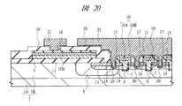
そこで、本実施の形態1では、図19に示すようなゲートフィンガー構造を採用する。すなわち、チップ領域CHPに沿って形成されたゲート配線21と一体に形成されたゲートフィンガー部(第2電極、第2部)21Aを設けるものである。なお、ゲート配線21およびゲートフィンガー部21Aと共に、ゲート配線21Bも一体に形成されている。ゲートフィンガー部21Aは、平面でゲート配線21からチップ領域CHPの内側へ向かって延在し、その下部には、ゲート電極10と電気的に接続する多結晶シリコンパターン11(図9参照)が配置されている。また、図示は省略するが、ゲートフィンガー部21Aは、ゲート配線21と同様に、絶縁膜16に開口されたコンタクト溝18(図9参照)を埋め込むように形成され、コンタクト溝18の底部で多結晶シリコンパターン11と接している。また、ゲートフィンガー部21Aは、ゲート配線21と一体に形成されていることから、Al膜を主導電層とする金属配線となる。このようなゲートフィンガー部21Aを設けることにより、多結晶シリコンパターン11をゲート配線21下まで延在させる代わりに、多結晶シリコンパターン11より抵抗率の低い金属配線であるゲートフィンガー部21Aを多結晶シリコンパターン11上まで延在させることになる。その結果、多結晶シリコンパターン11をゲート配線21下まで延在させる場合に比べて、上記ゲート抵抗Rgを低減することができる。なお、図19中のB−B線に沿った断面は、図9に示した断面図となる。 Therefore, in the first embodiment, a gate finger structure as shown in FIG. 19 is adopted. That is, a gate finger portion (second electrode, second portion) 21A formed integrally with the
また、図20および図21に示すように、ゲート電極10を多結晶シリコン層10A上にタングステンシリサイド層などのシリサイド層(シリコン化合物膜)10Bを積層した構造(図20)、または多結晶シリコン層10A上に窒化タングステン層(金属膜)10Cおよびタングステン層(金属膜)10Dを順次積層した構造(図21)としてもよい。このような構造のゲート電極10とすることによって、多結晶シリコン層のみからゲート電極10を形成した上記の本実施の形態1に比べてゲート電極10の抵抗率を下げることができるので、ゲート抵抗のさらなる低減が可能となる。また、ゲート電極10と多結晶シリコンパターン11とは、同じ工程で形成されるので、多結晶シリコンパターン11上にもシリサイド層10Bまたは窒化タングステン層10Cとタングステン層10Dとの積層膜が形成される。 20 and FIG. 21, the
ところで、前述したように、本実施の形態1において、p型半導体領域14は、p-型半導体領域13中に局所的に形成している。また、p型半導体領域14形成のための熱処理時間は短時間であることから、不純物イオンであるBイオンの打ち込みエネルギーでp型半導体領域14の形成位置および不純物濃度のピークを決定している。そのため、打ち込んだBイオンのチャネリングによる濃度分布の広がりが懸念される。Bイオンは、原子半径が小さいことから、特にチャネリングの影響を受けることが懸念される。Incidentally, as described above, in the first embodiment, the p-
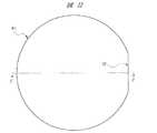
そこで、本実施の形態1においては、図1を用いて前述したように、基板1としてオフアングル基板を用いる。このオフアングル基板について、図22および図23を用いて説明する。なお、図23は、図22中のC−C線に沿った位置での断面図である。 Therefore, in the first embodiment, an off-angle substrate is used as the
図22および図23に示すように、(100)面を主面(素子形成面)とする第1のウエハW1において、その主面の法線をn1とする。また、法線n1から角度(第1の角度)θだけオリエンテーションフラットOFの方向に傾いた直線をn2とする。この直線n2が法線となる主面を有する第2のウエハがオフアングル基板である。本実施の形態1では、その角度θを約4°とすることを例示できる。 As shown in FIGS. 22 and 23, in the first wafer W1 having the (100) plane as the main surface (element formation surface), the normal line of the main surface is set to n1. Further, a straight line inclined in the direction of the orientation flat OF by an angle (first angle) θ from the normal line n1 is defined as n2. A second wafer having a main surface with the straight line n2 being a normal line is an off-angle substrate. In the first embodiment, it can be exemplified that the angle θ is about 4 °.
ここで、図24は、上記第1のウエハW1に不純物としてBイオンを主面に垂直な方向から導入した際における、基板(ウエハW1)表面からの深さと不純物濃度分布との関係を示したものであり、Bイオンの打ち込みエネルギーが60keV、200keVおよび1000keVの3通りの例について示している。また、図25は、上記角度θが4°のオフアングル基板である上記第2のウエハに不純物としてBイオンを主面に垂直な方向から導入した際における、基板(第2のウエハ)表面からの深さと不純物濃度分布との関係を示したものであり、Bイオンの打ち込みエネルギーが60keV、200keVおよび1000keVの3通りの例について示している。図24および図25に示すように、第2のウエハにBイオンを打ち込んだ場合には、第1のウエハにBイオンを打ち込んだ場合に比べて、濃度分布が急峻になっており、Bイオンの打ち込みエネルギーが大きくなるほどその傾向は強くなっている。すなわち、このようなオフアングル基板を上記基板1として用いることにより、基板1の主面に垂直な方向からBイオンを導入することでp型半導体領域14を形成する際に、導入したBイオンがチャネリングによって広がってしまうことを防ぐことができる。その結果、本実施の形態1によれば、p型半導体領域14をp-型半導体領域13中に局所的に形成することが可能となる。Here, FIG. 24 shows the relationship between the depth from the surface of the substrate (wafer W1) and the impurity concentration distribution when B ions as impurities are introduced into the first wafer W1 from the direction perpendicular to the main surface. 3 shows examples of B ion implantation energies of 60 keV, 200 keV and 1000 keV. FIG. 25 shows the surface of the substrate (second wafer) when B ions as impurities are introduced from the direction perpendicular to the main surface into the second wafer, which is an off-angle substrate having an angle θ of 4 °. 3 shows the relationship between the depth of impurity and the impurity concentration distribution, and shows three examples of B ion implantation energies of 60 keV, 200 keV and 1000 keV. As shown in FIGS. 24 and 25, when the B ions are implanted into the second wafer, the concentration distribution is steeper than when the B ions are implanted into the first wafer. The tendency becomes stronger as the driving energy increases. That is, by using such an off-angle substrate as the
図示は省略するが、上記ゲートパッドGP、ゲート配線21およびソースパッド22を形成した後、基板1の上部に、保護膜として、たとえばポリイミド樹脂膜を塗布し、露光、現像することによって、ゲート配線21およびソースパッド22上のポリイミド樹脂膜を除去し、開口部を形成する。 Although illustration is omitted, after forming the gate pad GP, the
次いで、基板1の表面をテープ等で保護した後、保護面を下側とし、n+型単結晶シリコン基板1Aの裏面を研削する。続いて、n+型単結晶シリコン基板1Aの裏面上に、導電性膜として、たとえばTi(チタン)膜、Ni(ニッケル)膜およびAu(金)膜を順次スパッタリング法により堆積し、これらの積層膜を形成する。この積層膜は、ドレイン(n+型単結晶シリコン基板1Aおよびn-型単結晶シリコン層1B)の引出し電極(ドレイン電極)となる。Next, after protecting the surface of the
続いて、上記テープを剥がし、上記ポリイミド樹脂膜に形成した開口部上に、たとえばAu等よりなるバンプ電極を形成した後、ウエハ状態の基板を、たとえば分割領域に沿ってダイシングし、個々のチップへと分割する。その後、個々のチップを、たとえば外部端子を有するリードフレーム(実装板)上に搭載し樹脂等で封止(実装)し、本実施の形態1の半導体装置を製造する。 Subsequently, the tape is peeled off, and bump electrodes made of, for example, Au are formed on the openings formed in the polyimide resin film, and then the substrate in the wafer state is diced along, for example, the divided regions, and individual chips are formed. Divide into Thereafter, the individual chips are mounted on, for example, a lead frame (mounting plate) having external terminals and sealed (mounted) with a resin or the like to manufacture the semiconductor device of the first embodiment.
(実施の形態2)
次に、本実施の形態2の半導体装置について説明する。(Embodiment 2)
Next, the semiconductor device of the second embodiment will be described.
図26に示すように、本実施の形態2においては、パワーMISFETのチャネル層となるp-型半導体領域13が溝7の側面を完全に覆うようにし、溝7の底部の全面または一部がn-型単結晶シリコン層1Bと接するようにしたものである。その他の構造は前記実施の形態1と同様である。このようなp-型半導体領域13を形成するには、たとえばp-型半導体領域13の形成時における熱処理の温度または熱処理時間を前記実施の形態1の条件から変えることによって実現することができる。このようなp-型半導体領域13とすることにより、前記実施の形態1に比べてp-型半導体領域13からn-型単結晶シリコン層1Bへはみ出している熱酸化膜9の表面積を小さくできる。それにより、本実施の形態2のパワーMISFETは、前記実施の形態1のパワーMISFETに比べて、ゲート絶縁膜(熱酸化膜9)を容量絶縁膜としゲート電極10を容量電極とする容量成分のうち、帰還容量を低減することができる。このような本実施の形態2のパワーMISFETをDC/DCコンバータ(図15参照)のスイッチング素子として用いた場合には、前記実施の形態1のパワーMISFETを用いた場合に比べて、さらにスイッチング損失を低減することが可能となる。As shown in FIG. 26, in the second embodiment, the p−
図26を用いて説明したような本実施の形態2のp-型半導体領域13は、導入した不純物イオンを拡散させることによって溝7の側面を完全に覆うように形成していることから、溝7の深さに製造上のばらつきが発生して、p-型半導体領域13が溝7の底部を覆ってしまう不具合も懸念される。そこで、図27に示すように、溝7の直下にp-型半導体領域13と導電型が逆かつ同程度の不純物濃度であり、n-型単結晶シリコン層1Bより不純物濃度の高いn-型半導体領域(第6半導体層)13Aを形成する。このn-型半導体領域13Aを設けることによって、p-型半導体領域13が溝7の底部を覆ってしまうことを防ぐことができる。それにより、溝7の深さに製造上のばらつきが発生した場合でも、p-型半導体領域13からn-型単結晶シリコン層1Bへはみ出している熱酸化膜9の表面積を一定に保つことができる。Since the p−
このようなn-型半導体領域13Aは、溝7を形成した後で、熱酸化膜9を形成する前に酸化シリコン膜3(図3参照)をマスクとして溝7の底部からn型の不純物イオン(たとえばAs)を導入することで形成することができる。また、酸化シリコン膜3をマスクとして不純物イオンを導入するので、その不純物イオンの導入時のマスクとするためのフォトレジスト膜を基板1上でパターニングする工程を省略することができる。すなわち、工程数としては、不純物イオン導入の1工程増やしただけでn-型半導体領域13Aを形成することができる。Such an n− -
ここで、図28は、図27を用いて説明したn-型半導体領域13Aを有する本実施の形態2のパワーMISFETおよび本発明者らが検討した第1のパワーMISFETのそれぞれについてのドレイン電圧と入力容量との関係を示したものである。また、図29は、図27を用いて説明したn-型半導体領域13Aを有する本実施の形態2のパワーMISFETおよび本発明者らが検討した第1のパワーMISFETのそれぞれについてのドレイン電圧と帰還容量との関係を示したものである。図28および図29に示すように、溝7が浅く形成され、p-型半導体領域13が溝7の側面を完全に覆い、溝7の直下にn-型半導体領域13Aが形成された本実施の形態2のパワーMISFETは、本発明者らが検討した第1のパワーMISFETに比べて入力容量および帰還容量の両方を低減することができる。すなわち、本実施の形態2のパワーMISFETをDC/DCコンバータ(図15)のスイッチング素子として用いた場合には、DC/DCコンバータの損失を大幅に低減することができる。それにより、DC/DCコンバータシステムの高効率化を実現することができる。Here, FIG. 28 shows the drain voltage for each of the power MISFET of the second embodiment having the n−
図30は、図27を用いて説明したn-型半導体領域13Aを有する本実施の形態2のパワーMISFETおよび本発明者らが検討した第1のパワーMISFETのそれぞれをDC/DCコンバータ(図15)のスイッチング素子として用いた際の、損失についての計算結果を示したものである。このときの計算条件は、入力電圧Vinを12V、出力電圧Voutを1.3V、出力電流Ioutを2A、および回路の動作周波数を1MHzとしている。本実施の形態2のパワーMISFETは、本発明者らが検討した第1のパワーMISFETに比べて溝7を浅く形成していることから、パワーMISFETの入力容量を低減することができる。それにより、図30に示すように、本実施の形態2のパワーMISFETを用いた場合には、本発明者らが検討した第1のパワーMISFETを用いた場合に比べてDC/DCコンバータのドライブ損失を低減することができ、本発明者らが行った計算によれば約20%低減することができる。30 shows a DC / DC converter (FIG. 15) for each of the power MISFET of the second embodiment having the n−
上記のような本実施の形態2によっても、前記実施の形態1と同様の効果を得ることができる。 According to the second embodiment as described above, the same effect as in the first embodiment can be obtained.
(実施の形態3)
次に、本実施の形態3の半導体装置について説明する。(Embodiment 3)
Next, the semiconductor device according to the third embodiment will be described.
図31に示すように、本実施の形態3においては、パワーMISFETのゲート電極10が形成される溝7を断面でV字状(底部に向かって細くなる順テーパー状)になるように形成したものである。その他の構造は前記実施の形態1と同様である。このような溝7を形成するには、溝7を形成する際の基板1のエッチングをKOH(水酸化カリウム)を用いたウェットエッチングとしたり、またはドライエッチングとしてその際のエッチングガスの組成比を調節することで実現することができる。このような溝7とすることにより、前記実施の形態1に比べてn+型半導体領域15下の溝7(熱酸化膜9)の表面積およびn-型単結晶シリコン層1Bと接する溝7(熱酸化膜9)の表面積を小さくできる。それにより、本実施の形態3によれば、前記実施の形態1に比べて入力容量および帰還容量の両方を低減することができる。すなわち、本実施の形態3のパワーMISFETをDC/DCコンバータ(図15参照)のスイッチング素子として用いた場合には、DC/DCコンバータの損失を大幅に低減することができる。それにより、DC/DCコンバータシステムの高効率化を実現することができる。As shown in FIG. 31, in the third embodiment, the
また、図32に示すように、溝7の直下に前記実施の形態2にて説明したn-型半導体領域13A(図27参照)と同様のn-型半導体領域13Aを形成する。このn-型半導体領域13Aは、溝7の底部を覆うように形成されているので、前記実施の形態2と同様に、p-型半導体領域13が溝7の底部を覆ってしまうことを防ぐことができる。それにより、p-型半導体領域13からn-型単結晶シリコン層1Bへはみ出している熱酸化膜9の表面積を一定に保つことができる。32, an n−
上記のような本実施の形態3によっても、前記実施の形態1と同様の効果を得ることができる。 According to the third embodiment as described above, the same effect as in the first embodiment can be obtained.
以上、本発明者によってなされた発明を実施の形態に基づき具体的に説明したが、本発明は前記実施の形態に限定されるものではなく、その要旨を逸脱しない範囲で種々変更可能であることはいうまでもない。 As mentioned above, the invention made by the present inventor has been specifically described based on the embodiment. However, the present invention is not limited to the embodiment, and various modifications can be made without departing from the scope of the invention. Needless to say.
本発明の半導体装置は、たとえばコンピュータの電源回路に用いられるDC/DCコンバータのスイッチング素子として用いることができる。 The semiconductor device of the present invention can be used as a switching element of a DC / DC converter used in a power supply circuit of a computer, for example.
1 半導体基板(基板)
1A n+型単結晶シリコン基板
1B n-型単結晶シリコン層(第1半導体層)
3 酸化シリコン膜
5 p型ウエル
7 溝(第1溝部)
9 熱酸化膜(第1絶縁膜)
10 ゲート電極(第1導電体)
10A 多結晶シリコン層
10B シリサイド層(シリコン化合物膜)
10C 窒化タングステン層(金属膜)
10D タングステン層(金属膜)
11 多結晶シリコンパターン
12 酸化シリコン膜
13 p-型半導体領域(第2半導体層)
13A n-型半導体領域(第6半導体層)
14 p型半導体領域(第5半導体層)
15 n+型半導体領域(第3半導体層)
16 絶縁膜
17 コンタクト溝(第2溝部)
18 コンタクト溝
20 p+型半導体領域(第4半導体層)
21 ゲート配線(第2電極、第1部)
21A ゲートフィンガー部(第2電極、第2部)
22 ソースパッド(第1電極)
101 n+型単結晶シリコン基板
102 n-型単結晶シリコン層
103 溝
104 ゲート絶縁膜
105 ゲート部
106 ソース電極
107 絶縁膜
108 溝
109 p-型半導体領域
110 p+型半導体領域
111 n+型半導体領域
CHP チップ領域
DEP 空乏層
GELE ゲート電極
GP ゲートパッド
L1、L2、L3 配線
NEPI n-型単結晶シリコン層
NSEM n+型半導体領域
OF オリエンテーションフラット
PBOD p-型半導体領域
QH High−sideMISFET
QL Low−sideMISFET
W1 第1のウエハ1 Semiconductor substrate (substrate)
1A n+ type single
3 Silicon oxide film 5 P-type well 7 Groove (first groove)
9 Thermal oxide film (first insulating film)
10 Gate electrode (first conductor)
10A
10C tungsten nitride layer (metal film)
10D tungsten layer (metal film)
11
13A n− type semiconductor region (sixth semiconductor layer)
14 p-type semiconductor region (fifth semiconductor layer)
15 n+ type semiconductor region (third semiconductor layer)
16 Insulating
18 contact groove 20 p+ type semiconductor region (fourth semiconductor layer)
21 Gate wiring (second electrode, first part)
21A Gate finger part (second electrode, second part)
22 Source pad (first electrode)
101 n+ type single crystal silicon substrate 102 n− type single
QL Low-side MISFET
W1 first wafer
Claims (13)
Translated fromJapanese半導体基板の主面に形成された第1導電型の第1半導体層と、
前記第1半導体層上に形成され、前記第1導電型とは逆の第2導電型の第2半導体層と、
前記半導体基板の主面に形成され、少なくとも底部の一部が前記第1半導体層と接し、深さが1μm以下である複数の第1溝部と、
前記第1溝部の側壁および底面に形成された第1絶縁膜と、
前記第1絶縁膜上に形成され、前記第1溝部を埋め込む第1導電体と、
前記第1溝部に隣接して前記第2半導体層内に形成され、前記第1導電型を有する第3半導体層と、
隣り合う前記第1溝部間の前記第2半導体層内に形成された前記第2導電型の第4半導体層と、
前記第3半導体層および前記第4半導体層と電気的に接続する第1電極とを有し、
前記第1半導体層および前記第3半導体層は、前記MISFETのソースまたはドレインを形成し、前記第2半導体層は、前記MISFETのチャネル形成領域を形成し、
前記第2半導体層内の前記第3半導体層の下部に前記第2半導体層より不純物濃度が高い前記第2導電型の第5半導体層が形成され、
前記第5半導体層はパンチスルーストッパー層を構成し、
前記第2半導体層はチャネル層を構成し、
前記第5半導体層は不純物濃度が一定部を有し、
前記第2半導体層は不純物濃度が深さ方向に減少する傾斜部を有し、
前記第1半導体層はドレイン領域を構成し、
前記第3半導体層はソース領域を構成し、
隣り合う前記第1溝部間にて前記半導体基板の主面から前記第3半導体層を貫通する第2溝部が形成され、
前記第4半導体層は前記第2溝部の底部を覆うように形成され、
前記第1電極は前記第2溝部を埋め込むように形成されていることを特徴とする半導体装置。A semiconductor device having a MISFET,
A first semiconductor layer of a first conductivity type formed on the main surface of the semiconductor substrate;
A second semiconductor layer formed on the first semiconductor layer and having a second conductivity type opposite to the first conductivity type;
A plurality of first grooves formed on the main surface of the semiconductor substrate, at least part of which is in contact with the first semiconductor layer and having a depth of 1 μm or less;
A first insulating film formed on a side wall and a bottom surface of the first groove,
A first conductor formed on the first insulating film and burying the first groove;
A third semiconductor layer formed in the second semiconductor layer adjacent to the first groove and having the first conductivity type;
A second semiconductor layer of the second conductivity type formed in the second semiconductor layer between the adjacent first groove portions;
A first electrode electrically connected to the third semiconductor layer and the fourth semiconductor layer;
The first semiconductor layer and the third semiconductor layer form a source or drain of the MISFET, the second semiconductor layer forms a channel formation region of the MISFET,
A fifth semiconductor layer of the second conductivity type having an impurity concentration higher than that of the second semiconductor layer is formed below the third semiconductor layer in the second semiconductor layer;
The fifth semiconductor layer constitutes a punch-through stopper layer;
The second semiconductor layer constitutes a channel layer;
The fifth semiconductor layer has a constant impurity concentration;
The second semiconductor layer has an inclined portion in which an impurity concentration decreases in a depth direction;
The first semiconductor layer constitutes a drain region;
The third semiconductor layer constitutes a source region;
A second groove portion penetrating the third semiconductor layer from the main surface of the semiconductor substrate is formed between the adjacent first groove portions;
The fourth semiconductor layer is formed to cover a bottom of the second groove;
The semiconductor device according to claim 1, wherein the first electrode is formed to fill the second groove .
前記MISFETはトレンチゲート型パワーMISFETであることを特徴とする半導体装置。The semiconductor device according to claim 1,
The semiconductor device, wherein the MISFET is a trench gate type power MISFET.
前記第1導電体と電気的に接続され、前記第1導電体より抵抗率の低い第2導電体から形成された第2電極を有することを特徴とする半導体装置。The semiconductor device according to claim 1,
A semiconductor device comprising: a second electrode formed of a second conductor that is electrically connected to the first conductor and has a lower resistivity than the first conductor.
前記MISFETは前記半導体基板のチップ領域に形成され、
前記第2電極は、前記チップ領域の周辺に沿って形成された第1部と、前記第1部より内側の前記チップ領域に延在する第2部とを有することを特徴とする半導体装置。The semiconductor device according to claim 3.
The MISFET is formed in a chip region of the semiconductor substrate,
2. The semiconductor device according to claim 1, wherein the second electrode has a first part formed along the periphery of the chip region and a second part extending to the chip region inside the first part.
前記第1溝部の深さは、前記第2半導体層の深さの1.1倍以下であることを特徴とする半導体装置。The semiconductor device according to claim 1,
The depth of the first trench is 1.1 times or less than the depth of the second semiconductor layer.
前記第1溝部の前記第2半導体層からのはみ出し量は0.1μm以下であることを特徴とする半導体装置。The semiconductor device according to claim 5.
An amount of protrusion of the first groove portion from the second semiconductor layer is 0.1 μm or less.
前記第1溝部の下部に前記第1溝部と接する前記第1導電型の第6半導体層が形成されていることを特徴とする半導体装置。The semiconductor device according to claim 1,
The semiconductor device according to claim 1, wherein a sixth semiconductor layer of the first conductivity type that is in contact with the first groove is formed below the first groove.
前記MISFETのしきい値電圧は2V以下であることを特徴とする半導体装置。The semiconductor device according to claim 1,
A semiconductor device, wherein a threshold voltage of the MISFET is 2 V or less.
前記MISFETはDC/DCコンバータのスイッチング素子として用いられることを特徴とする半導体装置。The semiconductor device according to claim 1,
The semiconductor device, wherein the MISFET is used as a switching element of a DC / DC converter.
(a)半導体基板の主面に第1導電型の第1半導体層を形成する工程、
(b)前記半導体基板の主面に複数の第1溝部を形成する工程、
(c)前記第1溝部内に第1絶縁膜を形成する工程、
(d)前記第1絶縁膜の存在下で前記第1溝部内に第1導電体を埋め込み、ゲート電極を形成する工程、
(e)前記(a)〜(d)工程後に、前記半導体基板に前記第1導電型とは逆の第2導電型の不純物を導入して、前記第1半導体層上に前記第2導電型の第2半導体層を形成する工程、
(f)前記(e)工程後に、前記半導体基板に熱処理を施す工程、
(g)前記(f)工程後に、前記半導体基板に前記第1導電型の不純物を導入し、前記第2半導体層上に前記第1溝部と隣接する前記第1導電型の第3半導体層を形成する工程、
(h)前記(f)工程後に、前記半導体基板に前記第1導電型とは逆の前記第2導電型の不純物を導入して、前記第2半導体層内の前記第3半導体層の下部に前記第2導電型の第5半導体層を形成する工程、
(i)前記(g)工程後および前記(h)工程後に、前記半導体基板に熱処理を施す工程、
(j)隣り合う前記ゲート電極間に配置されるように、前記半導体基板の主面に前記第3半導体層を貫通する複数の第2溝部を形成する工程、
(k)前記第2溝部の底部から前記半導体基板に前記第2導電型の不純物を導入し、前記第2半導体層内にて前記第2溝部の底部を覆うように前記第2導電型の第4半導体層を形成する工程、
(l)前記第2溝部を埋め込み、前記第3半導体層および前記第4半導体層と電気的に接続する第1電極を形成する工程、
を含み、
前記第1溝部は、少なくとも底部の一部が前記第1半導体層と接し、深さが1μm以下となるように形成し、
前記第5半導体層は、前記第2半導体層より不純物濃度が高くなるように形成し、
前記第1半導体層および前記第3半導体層が前記MISFETのソースまたはドレインとなり、前記第2半導体層が前記MISFETのチャネル形成領域となる前記MISFETを形成し、
前記第5半導体層はパンチスルーストッパー層を構成し、
前記第5半導体層は不純物濃度が一定部を有し、
前記第2半導体層は不純物濃度が深さ方向に減少する傾斜部を有することを特徴とする半導体装置の製造方法。A method of manufacturing a semiconductor device having a MISFET,
(A) forming a first semiconductor layer of the first conductivity type on the main surface of the semiconductor substrate;
(B) forming a plurality of first grooves on the main surface of the semiconductor substrate;
(C) forming a first insulating film in the first groove,
(D) burying a first conductor in the first trench in the presence of the first insulating film to form a gate electrode;
(E) After the steps (a) to (d), an impurity having a second conductivity type opposite to the first conductivity type is introduced into the semiconductor substrate, and the second conductivity type is formed on the first semiconductor layer. Forming a second semiconductor layer of
(F) a step of performing a heat treatment on the semiconductor substrate after the step (e);
(G) After the step (f), the first conductivity type impurity is introduced into the semiconductor substrate, and the first conductivity type third semiconductor layer adjacent to the first groove is formed on the second semiconductor layer. Forming step,
(H) After the step (f), an impurity of the second conductivity type opposite to the first conductivity type is introduced into the semiconductor substrate, and is formed below the third semiconductor layer in the second semiconductor layer. Forming a second semiconductor layer of the second conductivity type;
(I) a step of performing a heat treatment on the semiconductor substrate after the step (g) and after the step (h);
(J) forming a plurality of second grooves penetrating the third semiconductor layer in the main surface of the semiconductor substrate so as to be disposed between the adjacent gate electrodes;
(K) Impurities of the second conductivity type are introduced into the semiconductor substrate from the bottom of the second groove, and the second conductivity type second so as to cover the bottom of the second groove in the second semiconductor layer. 4 forming a semiconductor layer;
(L) forming a first electrode that fills the second groove and is electrically connected to the third semiconductor layer and the fourth semiconductor layer;
Including
The first groove is formed such that at least a part of the bottom is in contact with the first semiconductor layer and the depth is 1 μm or less.
The fifth semiconductor layer is formed to have a higher impurity concentration than the second semiconductor layer,
Forming the MISFET in which the first semiconductor layer and the third semiconductor layer serve as a source or drain of the MISFET, and the second semiconductor layer serves as a channel formation region of the MISFET;
The fifth semiconductor layer constitutes a punch-through stopper layer;
The fifth semiconductor layer has a constant impurity concentration;
The method of manufacturing a semiconductor device, wherein the second semiconductor layer has an inclined portion in which an impurity concentration decreases in a depth direction.
前記半導体基板は、(100)面の法線からオリエンテーションフラットまたはノッチの形成されている方向に第1の角度だけ傾けた直線を法線とする結晶面を主面とすることを特徴とする半導体装置の製造方法。The method of manufacturing a semiconductor device according to claim10 .
The semiconductor substrate is characterized in that a main surface is a crystal plane having a straight line inclined by a first angle in a direction in which an orientation flat or notch is formed from a normal line of (100) plane as a normal line. Device manufacturing method.
前記(b)工程は、前記第1溝部の底部から前記第1導電型の不純物を導入し、前記第1溝部の下部に前記第1溝部と接する前記第1導電型の第6半導体層を形成する工程を含むことを特徴とする半導体装置の製造方法。The method of manufacturing a semiconductor device according to claim10 .
In the step(b) , the first conductivity type impurity is introduced from the bottom of the first groove portion, and the first conductivity type sixth semiconductor layer in contact with the first groove portion is formed below the first groove portion. The manufacturing method of the semiconductor device characterized by including the process to do.
前記MISFETはトレンチゲート型パワーMISFETであることを特徴とする半導体装置の製造方法。The method of manufacturing a semiconductor device according to claim10 .
The method of manufacturing a semiconductor device, wherein the MISFET is a trench gate type power MISFET.
Priority Applications (5)
| Application Number | Priority Date | Filing Date | Title |
|---|---|---|---|
| JP2003286142AJP4945055B2 (en) | 2003-08-04 | 2003-08-04 | Semiconductor device and manufacturing method thereof |
| US10/886,041US20050029584A1 (en) | 2003-08-04 | 2004-07-08 | Semiconductor device and a method of manufacturing the same |
| US11/657,592US20070120194A1 (en) | 2003-08-04 | 2007-01-25 | Semiconductor device and a method of manufacturing the same |
| US12/385,979US7981747B2 (en) | 2003-08-04 | 2009-04-27 | Semiconductor device and a method of manufacturing the same |
| US13/067,566US20110233664A1 (en) | 2003-08-04 | 2011-06-09 | Semiconductor device and a method of manufacturing the same |
Applications Claiming Priority (1)
| Application Number | Priority Date | Filing Date | Title |
|---|---|---|---|
| JP2003286142AJP4945055B2 (en) | 2003-08-04 | 2003-08-04 | Semiconductor device and manufacturing method thereof |
Publications (2)
| Publication Number | Publication Date |
|---|---|
| JP2005057050A JP2005057050A (en) | 2005-03-03 |
| JP4945055B2true JP4945055B2 (en) | 2012-06-06 |
Family
ID=34113935
Family Applications (1)
| Application Number | Title | Priority Date | Filing Date |
|---|---|---|---|
| JP2003286142AExpired - Fee RelatedJP4945055B2 (en) | 2003-08-04 | 2003-08-04 | Semiconductor device and manufacturing method thereof |
Country Status (2)
| Country | Link |
|---|---|
| US (4) | US20050029584A1 (en) |
| JP (1) | JP4945055B2 (en) |
Families Citing this family (67)
| Publication number | Priority date | Publication date | Assignee | Title |
|---|---|---|---|---|
| JP4860122B2 (en)* | 2004-06-25 | 2012-01-25 | ルネサスエレクトロニクス株式会社 | Manufacturing method of semiconductor device |
| JP2006049341A (en)* | 2004-07-30 | 2006-02-16 | Renesas Technology Corp | Semiconductor device and manufacturing method thereof |
| US8283723B2 (en)* | 2005-02-11 | 2012-10-09 | Alpha & Omega Semiconductor Limited | MOS device with low injection diode |
| US7453119B2 (en)* | 2005-02-11 | 2008-11-18 | Alphs & Omega Semiconductor, Ltd. | Shielded gate trench (SGT) MOSFET cells implemented with a schottky source contact |
| US7285822B2 (en)* | 2005-02-11 | 2007-10-23 | Alpha & Omega Semiconductor, Inc. | Power MOS device |
| US7948029B2 (en) | 2005-02-11 | 2011-05-24 | Alpha And Omega Semiconductor Incorporated | MOS device with varying trench depth |
| US8362547B2 (en) | 2005-02-11 | 2013-01-29 | Alpha & Omega Semiconductor Limited | MOS device with Schottky barrier controlling layer |
| US8093651B2 (en)* | 2005-02-11 | 2012-01-10 | Alpha & Omega Semiconductor Limited | MOS device with integrated schottky diode in active region contact trench |
| US7786531B2 (en)* | 2005-03-18 | 2010-08-31 | Alpha & Omega Semiconductor Ltd. | MOSFET with a second poly and an inter-poly dielectric layer over gate for synchronous rectification |
| JP4955222B2 (en) | 2005-05-20 | 2012-06-20 | ルネサスエレクトロニクス株式会社 | Manufacturing method of semiconductor device |
| JP2008159916A (en) | 2006-12-25 | 2008-07-10 | Sanyo Electric Co Ltd | Semiconductor device |
| KR100824205B1 (en)* | 2006-12-26 | 2008-04-21 | 매그나칩 반도체 유한회사 | DMOS transistor and manufacturing method |
| KR100777593B1 (en)* | 2006-12-27 | 2007-11-16 | 동부일렉트로닉스 주식회사 | Trench gate MOS device and manufacturing method thereof |
| WO2008149800A1 (en)* | 2007-05-30 | 2008-12-11 | Rohm Co., Ltd. | Semiconductor device |
| JP5285874B2 (en) | 2007-07-03 | 2013-09-11 | ルネサスエレクトロニクス株式会社 | Manufacturing method of semiconductor device |
| KR100970282B1 (en)* | 2007-11-19 | 2010-07-15 | 매그나칩 반도체 유한회사 | Trench MOOSFET and its manufacturing method |
| CN101465376B (en)* | 2007-12-21 | 2012-07-04 | 万国半导体股份有限公司 | MOS device with low injection diode |
| US7977737B2 (en)* | 2008-03-06 | 2011-07-12 | Infineon Technologies Austria Ag | Semiconductor device having additional capacitance to inherent gate-drain or inherent drain-source capacitance |
| EP2293336B1 (en)* | 2008-05-20 | 2019-11-27 | Rohm Co., Ltd. | Semiconductor device |
| JP5239548B2 (en)* | 2008-06-25 | 2013-07-17 | 富士通セミコンダクター株式会社 | Semiconductor device and manufacturing method of semiconductor device |
| JP5297104B2 (en) | 2008-07-01 | 2013-09-25 | ルネサスエレクトロニクス株式会社 | Semiconductor device |
| US8193579B2 (en) | 2008-07-29 | 2012-06-05 | Rohm Co., Ltd. | Trench type semiconductor device and fabrication method for the same |
| US8362552B2 (en)* | 2008-12-23 | 2013-01-29 | Alpha And Omega Semiconductor Incorporated | MOSFET device with reduced breakdown voltage |
| CN101710586B (en)* | 2009-01-09 | 2011-12-28 | 深超光电(深圳)有限公司 | Storage capacitor for improving aperture opening ratio and manufacturing method thereof |
| US8846473B2 (en)* | 2009-06-01 | 2014-09-30 | Sensor Electronic Technology, Inc. | Low-resistance electrode design |
| US8168497B2 (en)* | 2009-06-01 | 2012-05-01 | Sensor Electronic Technology, Inc. | Low-resistance electrode design |
| JP2011009352A (en) | 2009-06-24 | 2011-01-13 | Renesas Electronics Corp | Semiconductor device, method of manufacturing the same, and power supply device using the same |
| US8058674B2 (en)* | 2009-10-07 | 2011-11-15 | Moxtek, Inc. | Alternate 4-terminal JFET geometry to reduce gate to source capacitance |
| US9425305B2 (en) | 2009-10-20 | 2016-08-23 | Vishay-Siliconix | Structures of and methods of fabricating split gate MIS devices |
| US9419129B2 (en) | 2009-10-21 | 2016-08-16 | Vishay-Siliconix | Split gate semiconductor device with curved gate oxide profile |
| KR101728363B1 (en) | 2010-03-02 | 2017-05-02 | 비쉐이-실리코닉스 | Structures and methods of fabricating dual gate devices |
| JP5662865B2 (en)* | 2010-05-19 | 2015-02-04 | ルネサスエレクトロニクス株式会社 | Semiconductor device and manufacturing method thereof |
| US9653597B2 (en) | 2010-05-20 | 2017-05-16 | Infineon Technologies Americas Corp. | Method for fabricating a shallow and narrow trench FET and related structures |
| JP5616720B2 (en)* | 2010-08-30 | 2014-10-29 | セイコーインスツル株式会社 | Semiconductor device and manufacturing method thereof |
| JP5674530B2 (en) | 2010-09-10 | 2015-02-25 | ルネサスエレクトロニクス株式会社 | Control device for semiconductor device |
| JP5638340B2 (en)* | 2010-10-20 | 2014-12-10 | ルネサスエレクトロニクス株式会社 | Semiconductor device |
| JP5574923B2 (en)* | 2010-11-10 | 2014-08-20 | 三菱電機株式会社 | Semiconductor device and manufacturing method thereof |
| JP5694119B2 (en)* | 2010-11-25 | 2015-04-01 | 三菱電機株式会社 | Silicon carbide semiconductor device |
| US20120175699A1 (en)* | 2011-01-06 | 2012-07-12 | Force Mos Technology Co., Ltd. | Trench mosfet with super pinch-off regions and self-aligned trenched contact |
| CN102184945A (en)* | 2011-05-03 | 2011-09-14 | 成都芯源系统有限公司 | Groove gate type MOSFET device |
| DE112012002136B4 (en) | 2011-05-18 | 2025-03-27 | Vishay-Siliconix | Semiconductor devices |
| JP5677222B2 (en) | 2011-07-25 | 2015-02-25 | 三菱電機株式会社 | Silicon carbide semiconductor device |
| JP6290526B2 (en)* | 2011-08-24 | 2018-03-07 | ローム株式会社 | Semiconductor device and manufacturing method thereof |
| US8368192B1 (en)* | 2011-09-16 | 2013-02-05 | Powertech Technology, Inc. | Multi-chip memory package with a small substrate |
| US8716787B2 (en)* | 2012-03-27 | 2014-05-06 | Super Group Semiconductor Co., Ltd. | Power semiconductor device and fabrication method thereof |
| US9000497B2 (en)* | 2012-09-14 | 2015-04-07 | Renesas Electronics Corporation | Trench MOSFET having an independent coupled element in a trench |
| US9105713B2 (en) | 2012-11-09 | 2015-08-11 | Infineon Technologies Austria Ag | Semiconductor device with metal-filled groove in polysilicon gate electrode |
| JP5876008B2 (en)* | 2013-06-03 | 2016-03-02 | ルネサスエレクトロニクス株式会社 | Semiconductor device |
| TWI487115B (en)* | 2013-06-07 | 2015-06-01 | Sinopower Semiconductor Inc | Ditch type power element and manufacturing method thereof |
| US20150118810A1 (en)* | 2013-10-24 | 2015-04-30 | Madhur Bobde | Buried field ring field effect transistor (buf-fet) integrated with cells implanted with hole supply path |
| JP6356803B2 (en)* | 2013-11-29 | 2018-07-11 | アーベーベー・テクノロジー・アーゲー | Insulated gate bipolar transistor |
| US9773863B2 (en)* | 2014-05-14 | 2017-09-26 | Infineon Technologies Austria Ag | VDMOS having a non-depletable extension zone formed between an active area and side surface of semiconductor body |
| US10468479B2 (en) | 2014-05-14 | 2019-11-05 | Infineon Technologies Austria Ag | VDMOS having a drift zone with a compensation structure |
| US10234486B2 (en) | 2014-08-19 | 2019-03-19 | Vishay/Siliconix | Vertical sense devices in vertical trench MOSFET |
| TWI581425B (en)* | 2015-11-24 | 2017-05-01 | Macroblock Inc | And a power semiconductor device having an edge terminal structure having a gradation concentration |
| DE102016101801B4 (en)* | 2016-02-02 | 2021-01-14 | Infineon Technologies Ag | LOAD CONNECTION OF A POWER SEMICONDUCTOR ELEMENT, POWER SEMICONDUCTOR MODULE WITH IT AND MANUFACTURING PROCESS FOR IT |
| US10950494B2 (en)* | 2018-01-19 | 2021-03-16 | Infineon Technologies Ag | Semiconductor device including first and second contact layers and manufacturing method |
| JP6994991B2 (en)* | 2018-03-16 | 2022-02-04 | 株式会社 日立パワーデバイス | Semiconductor devices, power modules and power converters |
| JP7272071B2 (en)* | 2019-04-04 | 2023-05-12 | 富士電機株式会社 | Semiconductor device and method for manufacturing semiconductor device |
| US11362209B2 (en)* | 2019-04-16 | 2022-06-14 | Semiconductor Components Industries, Llc | Gate polysilicon feed structures for trench devices |
| US11217541B2 (en) | 2019-05-08 | 2022-01-04 | Vishay-Siliconix, LLC | Transistors with electrically active chip seal ring and methods of manufacture |
| US11218144B2 (en) | 2019-09-12 | 2022-01-04 | Vishay-Siliconix, LLC | Semiconductor device with multiple independent gates |
| JP7120192B2 (en)* | 2019-09-17 | 2022-08-17 | 株式会社デンソー | semiconductor equipment |
| TWI739252B (en)* | 2019-12-25 | 2021-09-11 | 杰力科技股份有限公司 | Trench mosfet and manufacturing method of the same |
| US20210343847A1 (en)* | 2020-04-30 | 2021-11-04 | Cree, Inc. | Diffusion and/or enhancement layers for electrical contact regions |
| US11685609B2 (en)* | 2020-11-27 | 2023-06-27 | Terry Michael Brown, SR. | Split drive sprocket assembly |
| JP7623267B2 (en)* | 2021-11-05 | 2025-01-28 | ルネサスエレクトロニクス株式会社 | Semiconductor device manufacturing method |
Family Cites Families (18)
| Publication number | Priority date | Publication date | Assignee | Title |
|---|---|---|---|---|
| JPS60186068A (en)* | 1985-01-31 | 1985-09-21 | Hitachi Ltd | Insulated gate field effect transistor |
| US5282018A (en)* | 1991-01-09 | 1994-01-25 | Kabushiki Kaisha Toshiba | Power semiconductor device having gate structure in trench |
| JPH0653514A (en)* | 1992-08-03 | 1994-02-25 | Nippon Telegr & Teleph Corp <Ntt> | Method for manufacturing semiconductor device |
| JP3167457B2 (en) | 1992-10-22 | 2001-05-21 | 株式会社東芝 | Semiconductor device |
| GB9313843D0 (en)* | 1993-07-05 | 1993-08-18 | Philips Electronics Uk Ltd | A semiconductor device comprising an insulated gate field effect transistor |
| WO1998012741A1 (en)* | 1996-09-18 | 1998-03-26 | Advanced Micro Devices, Inc. | Short channel non-self aligned vmos field effect transistor |
| US6084264A (en)* | 1998-11-25 | 2000-07-04 | Siliconix Incorporated | Trench MOSFET having improved breakdown and on-resistance characteristics |
| DE59814430D1 (en) | 1998-12-18 | 2010-03-25 | Infineon Technologies Ag | FIELD EFFECT TRANSISTOR ARRANGEMENT WITH A TRIANGULAR GATE ELECTRODE AND AN ADDITIONAL HIGH DEFINED LAYER IN THE BODY FIELD |
| JP2000269487A (en)* | 1999-03-15 | 2000-09-29 | Toshiba Corp | Semiconductor device and manufacturing method thereof |
| JP2000269518A (en)* | 1999-03-18 | 2000-09-29 | Toshiba Corp | Power semiconductor element and method of forming semiconductor layer |
| US20010001494A1 (en) | 1999-04-01 | 2001-05-24 | Christopher B. Kocon | Power trench mos-gated device and process for forming same |
| US6348712B1 (en) | 1999-10-27 | 2002-02-19 | Siliconix Incorporated | High density trench-gated power MOSFET |
| JP3884206B2 (en)* | 2000-01-20 | 2007-02-21 | 株式会社東芝 | Semiconductor device |
| JP4179491B2 (en)* | 2000-04-25 | 2008-11-12 | 株式会社ルネサステクノロジ | Semiconductor device, manufacturing method thereof, and characteristic evaluation method thereof |
| JP4150496B2 (en)* | 2000-12-28 | 2008-09-17 | 株式会社日立製作所 | Semiconductor device and manufacturing method thereof |
| JP3531613B2 (en)* | 2001-02-06 | 2004-05-31 | 株式会社デンソー | Trench gate type semiconductor device and manufacturing method thereof |
| JP2002270825A (en)* | 2001-03-08 | 2002-09-20 | Hitachi Ltd | Field effect transistor and method of manufacturing semiconductor device |
| JP4025063B2 (en)* | 2001-12-06 | 2007-12-19 | 株式会社ルネサステクノロジ | Semiconductor device |
- 2003
- 2003-08-04JPJP2003286142Apatent/JP4945055B2/ennot_activeExpired - Fee Related
- 2004
- 2004-07-08USUS10/886,041patent/US20050029584A1/ennot_activeAbandoned
- 2007
- 2007-01-25USUS11/657,592patent/US20070120194A1/ennot_activeAbandoned
- 2009
- 2009-04-27USUS12/385,979patent/US7981747B2/ennot_activeExpired - Lifetime
- 2011
- 2011-06-09USUS13/067,566patent/US20110233664A1/ennot_activeAbandoned
Also Published As
| Publication number | Publication date |
|---|---|
| US20070120194A1 (en) | 2007-05-31 |
| JP2005057050A (en) | 2005-03-03 |
| US20050029584A1 (en) | 2005-02-10 |
| US20110233664A1 (en) | 2011-09-29 |
| US7981747B2 (en) | 2011-07-19 |
| US20090212358A1 (en) | 2009-08-27 |
Similar Documents
| Publication | Publication Date | Title |
|---|---|---|
| JP4945055B2 (en) | Semiconductor device and manufacturing method thereof | |
| JP5285874B2 (en) | Manufacturing method of semiconductor device | |
| JP4892172B2 (en) | Semiconductor device and manufacturing method thereof | |
| US9356122B2 (en) | Through silicon via processing method for lateral double-diffused MOSFETs | |
| CN102376765B (en) | Semiconductor device and method for manufacturing the same | |
| JP4198469B2 (en) | Power device and manufacturing method thereof | |
| US7282765B2 (en) | Power LDMOS transistor | |
| JPH11284174A (en) | Field-coupled power MOSFET bus architecture using trench technology | |
| JP2006202931A (en) | Semiconductor device and manufacturing method thereof | |
| JP2002158353A (en) | MOS field effect transistor | |
| JP5684085B2 (en) | Semiconductor device | |
| JP4025063B2 (en) | Semiconductor device | |
| US20010023957A1 (en) | Trench-gate semiconductor devices | |
| JP2007281512A (en) | Semiconductor device | |
| JP5876008B2 (en) | Semiconductor device | |
| JP2023069620A (en) | Semiconductor device | |
| TWI385802B (en) | High-voltage metal-oxide semiconductor device and fabrication method thereof | |
| TWI836520B (en) | Semiconductor device and fabrication method thereof | |
| US12402368B2 (en) | Semiconductor device and method of manufacturing the same | |
| CN117673128A (en) | Semiconductor device with a semiconductor layer having a plurality of semiconductor layers | |
| KR100479426B1 (en) | High-Voltage Device Structure and It's Fabrication Process | |
| CN104769715B (en) | Power device integration on a common substrate | |
| CN117497586A (en) | Semiconductor device and method for manufacturing the same | |
| CN101728430A (en) | High voltage metal oxide semiconductor assembly and manufacturing method thereof | |
| CN117995843A (en) | Semiconductor device and method for manufacturing the same |
Legal Events
| Date | Code | Title | Description |
|---|---|---|---|
| A621 | Written request for application examination | Free format text:JAPANESE INTERMEDIATE CODE: A621 Effective date:20060802 | |
| A977 | Report on retrieval | Free format text:JAPANESE INTERMEDIATE CODE: A971007 Effective date:20100521 | |
| A711 | Notification of change in applicant | Free format text:JAPANESE INTERMEDIATE CODE: A712 Effective date:20100528 | |
| A131 | Notification of reasons for refusal | Free format text:JAPANESE INTERMEDIATE CODE: A131 Effective date:20100921 | |
| A521 | Request for written amendment filed | Free format text:JAPANESE INTERMEDIATE CODE: A523 Effective date:20101122 | |
| A131 | Notification of reasons for refusal | Free format text:JAPANESE INTERMEDIATE CODE: A131 Effective date:20110614 | |
| A521 | Request for written amendment filed | Free format text:JAPANESE INTERMEDIATE CODE: A523 Effective date:20110802 | |
| TRDD | Decision of grant or rejection written | ||
| A01 | Written decision to grant a patent or to grant a registration (utility model) | Free format text:JAPANESE INTERMEDIATE CODE: A01 Effective date:20120207 | |
| A01 | Written decision to grant a patent or to grant a registration (utility model) | Free format text:JAPANESE INTERMEDIATE CODE: A01 | |
| A61 | First payment of annual fees (during grant procedure) | Free format text:JAPANESE INTERMEDIATE CODE: A61 Effective date:20120305 | |
| R150 | Certificate of patent or registration of utility model | Ref document number:4945055 Country of ref document:JP Free format text:JAPANESE INTERMEDIATE CODE: R150 Free format text:JAPANESE INTERMEDIATE CODE: R150 | |
| FPAY | Renewal fee payment (event date is renewal date of database) | Free format text:PAYMENT UNTIL: 20150309 Year of fee payment:3 | |
| S531 | Written request for registration of change of domicile | Free format text:JAPANESE INTERMEDIATE CODE: R313531 | |
| R350 | Written notification of registration of transfer | Free format text:JAPANESE INTERMEDIATE CODE: R350 | |
| LAPS | Cancellation because of no payment of annual fees |