JP4943780B2 - Plasma processing apparatus and plasma processing method - Google Patents
Plasma processing apparatus and plasma processing methodDownload PDFInfo
- Publication number
- JP4943780B2 JP4943780B2JP2006235103AJP2006235103AJP4943780B2JP 4943780 B2JP4943780 B2JP 4943780B2JP 2006235103 AJP2006235103 AJP 2006235103AJP 2006235103 AJP2006235103 AJP 2006235103AJP 4943780 B2JP4943780 B2JP 4943780B2
- Authority
- JP
- Japan
- Prior art keywords
- plasma
- plasma processing
- substrate
- frequency power
- processed
- Prior art date
- Legal status (The legal status is an assumption and is not a legal conclusion. Google has not performed a legal analysis and makes no representation as to the accuracy of the status listed.)
- Expired - Fee Related
Links
Images


Landscapes
- Plasma Technology (AREA)
- Drying Of Semiconductors (AREA)
Description
Translated fromJapanese本発明は、プラズマ処理装置およびプラズマ処理方法に係り、特に高周波電力を印加して減圧下で着火したプラズマを用いて被処理物を処理するのに好適なプラズマ処理装置およびプラズマ処理方法に関する。 The present invention relates to a plasma processing apparatus and a plasma processing method, and more particularly to a plasma processing apparatus and a plasma processing method suitable for processing an object to be processed using plasma ignited under reduced pressure by applying high-frequency power.
従来、プラズマ処理装置における異物発生の要因として、(1)ガス起因のパーティクル、(2)ESC起因のパーティクル、(3)RF起因のパーティクル、(4)熱起因のパーティクル等があることが知られている。一般に、ESC起因のパーティクルに対しては、プラズマ着火後にESC電圧を印加することによりパーティクルを低減できることが知られている。 Conventionally, it is known that there are (1) particles caused by gas, (2) particles caused by ESC, (3) particles caused by RF, (4) particles caused by heat, and the like as factors of foreign matter generation in a plasma processing apparatus. ing. In general, it is known that for particles caused by ESC, the particles can be reduced by applying an ESC voltage after plasma ignition.
また、RF起因のパーティクルに対しては、最初に最小限プラズマの着火に必要な最小限の電力をガスに供給し最小限プラズマを生成し、その後電力を増加して被処理基板の処理に必要なプラズマを生成することにより、プラズマ着火時におけるパーティクルの発生自体を抑制し、発生したとしても被処理基板への付着を防止してパーティクルを低減できることが知られている(例えば、特許文献1参照)。
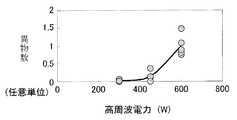
従来の異物低減技術は、プラズマ着火時におけるプラズマ着火遅れに伴う異物の発生、付着に関して考慮されていない。すなわち、電力(高周波電力)投入からプラズマ着火までの間にも異物が発生し、プラズマ着火後にも影響していることが発明者らの実験によって明らかになった。図1は電力投入からプラズマの発生までの異物と時間との関係を示した概念図であり、図2はプラズマが着火しない条件で電力のみを投入し、異物数を計測した結果である。 In the conventional foreign matter reduction technology, no consideration is given to the generation and adhesion of foreign matters accompanying plasma ignition delay during plasma ignition. That is, it has been clarified by experiments by the inventors that foreign matters are generated between the time when electric power (high-frequency power) is turned on and the plasma is ignited, and the influence is exerted after the plasma is ignited. FIG. 1 is a conceptual diagram showing the relationship between foreign matter and time from power-on to plasma generation, and FIG. 2 shows the result of measuring the number of foreign matters when only power is turned on under the condition that plasma does not ignite.
図2に示すようにプラズマの着火を伴わない電力投入だけでも異物が発生し、電力値が大きくなるに従い異物の量も多くなっている。この異物発生の機構については不明であるが、熱応力や静電応力、マックスウェル応力等が処理室内壁に働き、処理室内壁に付着していた異物が剥離等により発生したことが考えられる。 As shown in FIG. 2, foreign matter is generated only by turning on power without plasma ignition, and the amount of foreign matter increases as the power value increases. Although the mechanism of the generation of foreign matter is unknown, it is considered that thermal stress, electrostatic stress, Maxwell stress, etc. acted on the processing chamber inner wall and the foreign material adhering to the processing chamber inner wall was generated by peeling or the like.
図1に示すように電力投入により発生した異物は、発生場所からある初速を持って飛散、浮遊した後、基板に到達し、その一部が基板に付着する。高電力を投入すると異物の発生数が多いため、基板に付着する異物数も多くなるが、異物の剥離から基板へ到達するまでの間には異物の付着はない。電力投入からプラズマ着火までに時間がかかると、電力投入により処理室内壁面から剥離した異物が処理室空間に放出され被処理基板に付着してしまうという問題が生じる。 As shown in FIG. 1, the foreign matter generated by turning on the electric power is scattered and floated at a certain initial speed from the place of occurrence, and then reaches the substrate, and a part thereof adheres to the substrate. When high power is applied, the number of foreign matters generated is large, so the number of foreign matters attached to the substrate also increases. However, no foreign matter adheres between the separation of the foreign matter and the arrival at the substrate. When it takes a long time from turning on the power to igniting the plasma, there arises a problem that the foreign matter peeled off from the wall surface of the processing chamber due to turning on the power is released into the processing chamber space and adheres to the substrate to be processed.
本発明の目的は、プラズマ着火までに生じる被処理基板への異物の付着を抑制し異物の低減を図ることのできるプラズマ処理装置及びプラズマ処理方法を提供することにある。 An object of the present invention is to provide a plasma processing apparatus and a plasma processing method capable of suppressing the adhesion of foreign matter to a substrate to be processed that occurs until plasma ignition and reducing the foreign matter.
上記目的は、処理室内のガスに高周波電力を投入してプラズマを着火し、該プラズマを用いて被処理基板を処理するものにおいて、ガスへの高周波電力投入からプラズマが着火するまでの時間を、異物が被処理基板に到達するまでの時間内にすることにより達成される。 The above object is to ignite plasma by applying high-frequency power to the gas in the processing chamber, and to process the substrate to be processed using the plasma, in the time from the high-frequency power input to the gas until the plasma ignites, This is achieved by setting the time until the foreign material reaches the substrate to be processed.
また、上記目的は、プラズマの着火と異物が被処理基板に到達する時刻が同程度の場合には、プラズマの着火時に被処理基板にバイアス電位を与えることにより、より確実に達成される。 Further, the above object can be achieved more reliably by applying a bias potential to the substrate to be processed when the plasma is ignited when the time of plasma ignition and the time when the foreign matter reaches the substrate to be processed is approximately the same.
本発明によれば、高周波電力が投入されて処理室内に異物が放出されても、異物が被処理基板に到達するまでにプラズマが着火するため、処理室空間に放出された異物はシースの作用によって処理室空間に閉じ込められ被処理基板に到達することがないので、被処理基板への異物の付着を抑制でき、異物の低減を図ることができる。 According to the present invention, even if foreign matter is released into the processing chamber by applying high-frequency power, the plasma is ignited before the foreign matter reaches the substrate to be processed. Thus, the substrate is confined in the processing chamber space and does not reach the substrate to be processed, so that the adhesion of foreign matter to the substrate to be processed can be suppressed, and foreign matter can be reduced.
また、被処理基板にバイアス電位を与えることで被処理基板上に形成されるシースを厚くすることができ、被処理基板への異物の付着をより確実に抑制できる。 Further, by applying a bias potential to the substrate to be processed, the sheath formed on the substrate to be processed can be thickened, and adhesion of foreign matters to the substrate to be processed can be more reliably suppressed.
本発明は、図1に示したように異物が被処理基板に到達するまでの時間(この場合、たとえば0.9sec(処理室内圧力:0.1〜10Pa))以内にプラズマを着火する。これにより、高周波電力値が大きい場合(異物量が多い場合)でも小さい場合(異物量が少ない場合)でも関係なく、異物は被処理基板に到達することなくプラズマのシースの作用によって処理室内の空間に閉じ込められ、被処理基板への異物の付着を抑制することができる。 In the present invention, as shown in FIG. 1, the plasma is ignited within a time until the foreign substance reaches the substrate to be processed (in this case, for example, 0.9 sec (pressure in the processing chamber: 0.1 to 10 Pa)). Accordingly, regardless of whether the high-frequency power value is large (when the amount of foreign matter is large) or small (when the amount of foreign matter is small), the foreign matter does not reach the substrate to be processed, and the space in the processing chamber is caused by the action of the plasma sheath. It is possible to suppress the adhesion of foreign matter to the substrate to be processed.
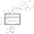
本発明のプラズマ処理装置の第1の実施例を、図3ないし図6により説明する。図3は、実施例1に係るプラズマ処理装置の概略構成を示す縦断面図である。図3の装置において、1は処理室であり、この場合、図示を省略した真空排気系が接続されている。処理室1内の下部には被処理基板5が配置される基板電極2が設けられている。基板電極2には整合器3を介して高周波バイアス電源4が接続されている。また、処理室1内の基板電極2に対向して高周波導入窓およびシャワープレート6及び電極7が設けられている。高周波導入窓およびシャワープレート6には、図示を省略したガス供給系が接続され、処理室に処理ガスをシャワー状に供給する。アンテナ7には整合器8を介して高周波電源9が接続されている。 A first embodiment of the plasma processing apparatus of the present invention will be described with reference to FIGS. FIG. 3 is a longitudinal sectional view illustrating a schematic configuration of the plasma processing apparatus according to the first embodiment. In the apparatus of FIG. 3,
整合器8および高周波電源9にはこの場合、プラズマの着火を容易にして着火時間を短くするための制御装置10が接続されている。制御装置10は高周波電源9からアンテナ7を介して処理室1内に電力を投入した際の反射電力を小さくするための整合器8を初期設定することが可能である。 In this case, a
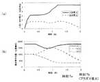
図4(a)に示すように、処理室内に所定のガスを所定の流量供給し真空排気系の排気速度を制御して所定の圧力に調整した後、高周波電源9を時刻ゼロにてオンし第1レベルの入射電力を投入する(図5のステップ101)。これにより反射電力が生じるが、図4(b)に示すように整合器の整合素子位置を自動整合させることにより反射電力を抑え(図5のステップ102)、反射電力が安定した時点でさらに高周波電力を上げ処理時の所定の電力量にする(図5のステップ103)。整合器8はさらに自動整合され所定の入射電力での反射電力が最小となる最適な整合値を得る(図5のステップ104)。これにより、処理室1内に効率良く電力が投入され処理室1内のガスがプラズマ化される(時刻Tb)。 As shown in FIG. 4 (a), a predetermined gas is supplied into the processing chamber at a predetermined flow rate, the exhaust speed of the vacuum exhaust system is controlled and adjusted to a predetermined pressure, and then the high
このとき、制御装置10は、図4におけるプラズマ着火(時刻Tb)前の時刻Taにおける整合器8の設定値、この場合、VC1,VC2,VC3の値を制御装置10に記憶する(図5のステップ105)。(時刻Tb−時刻Ta)は、図1に示す電力を投入してから異物が基板に到達するまでの時間内に設定される。好ましくは、プラズマが着火されてからプラズマが安定するのに要する時間(Tx)を考慮し、(時刻Tb−時刻Ta+時間Tx)が、異物が基板に到達するまでの時間内に設定されることが望ましい。制御装置10による整合器8の設定値の記憶は、被処理基板の処理条件が変更される毎に行われ、処理の種類毎に最適な設定値を記憶する。被処理基板の処理を実行する際には、制御装置10は、予め記憶した設定値によって整合器8を設定する(図5のステップ106)。これにより、高周波電源9からの出力を処理時の所定電力値で出力しても整合が容易であり、整合のための時間を短縮することができる。 At this time, the
これにより、電力投入からプラズマ着火までの時間を短縮することができ、電力投入により処理室内壁面から剥離された異物が処理室内に放出され基板に到達するまでに処理室内にプラズマを着火できる。これにより、処理室内に放出された異物はプラズマシースの作用によってプラズマ内に閉じ込められ、基板に到達して付着することがない。 Thereby, the time from power-on to plasma ignition can be shortened, and the plasma can be ignited before the foreign matter separated from the wall surface of the process chamber is released into the process chamber and reaches the substrate. Accordingly, the foreign matter released into the processing chamber is confined in the plasma by the action of the plasma sheath, and does not reach the substrate and adhere to it.
上述の実施例では、制御装置10による整合器8の設定値の記憶は、被処理基板の処理条件が変更される毎に行ったが、部品の変更や交換等のハード変更を伴わない場合には、必ずしも毎回行う必要はなく、初回のみ行ってもよい。例えば処理室の圧力をプラズマ着火により適した圧力に変更した場合、プラズマ着火前の処理室のインピーダンスには影響がないため、高周波電力の投入からプラズマ着火直前までの入反射電力や整合器の整合素子の動作に違いはない。ただしプラズマ着火に最低限必要な投入電力が小さくなるため、図4に示すプラズマ着火時刻Tbが早まることになる。ガス種やガス種の混合比等を変更した場合も同様にプラズマ着火前の処理室のインピーダンスに影響を与えないため、プラズマ着火直前までの入反射電力や整合器の整合素子の動作に違いはなく、プラズマ着火性が変化することによりプラズマ着火時刻が変わる事になる。プラズマ着火時刻が変わることは、プラズマ着火時の整合器の整合素子位置が変化することにつながる。高周波電力の投入からプラズマ着火までの時間(着火遅れ時間)を短縮する必要性がそれほど高くない場合には、ハード変更を伴う場合のみ、制御装置10による整合器8の設定値の記憶を行えばよい。 In the above-described embodiment, the setting value of the matching
図6に、制御装置10による整合器8の設定値の記憶を行うことで着火遅れ時間を短縮した場合(初期設定あり)と、整合器8の設定値の最適化を行わない場合(初期設定無し)の両者で異物数を比較した結果を示す。異物数の評価は被処理基板に付着した異物数を、ウェハ表面検査装置LS6600(日立電子エンジニアリング社製)を用いて計測した。一般に異物数は、ばらつきが大きいほか、装置の状態に依存し、装置状態の変動に伴い経時的に変化する。これに対応し、初期設定なしと初期設定ありの2条件を交互に繰り返して測定することで、両者の差異を調べた。初期設定なしに対して初期設定ありで異物数の平均値はおよそ半減しており、整合器設定値の初期設定により異物低減できることを確認した。 FIG. 6 shows the case where the ignition delay time is shortened by storing the setting value of the
本発明の第2の実施例を、図7ないし図9により説明する。図7は、実施例2に係るプラズマ処理装置の概略構成を示す縦断面図である。図7において、図3と同一符号は同一部材を示し、説明を省略する。図7において図3と異なる点は、プラズマの着火に磁場を用いる点と、磁場を最適化してプラズマの着火を容易にし、着火時間を短縮する点にある。図7において、処理室1の上部外側には磁場発生装置11が設けられている。磁場発生装置11には磁場発生用電源12が接続され、磁場発生用電源12には制御装置13が接続され、磁場強度および磁場勾配を調整可能になっている。また、制御装置13は高周波電源5の制御も行う。 A second embodiment of the present invention will be described with reference to FIGS. FIG. 7 is a longitudinal sectional view illustrating a schematic configuration of the plasma processing apparatus according to the second embodiment. 7, the same reference numerals as those in FIG. 3 denote the same members, and a description thereof is omitted. 7 differs from FIG. 3 in that a magnetic field is used for plasma ignition, and that the magnetic field is optimized to facilitate plasma ignition and shorten the ignition time. In FIG. 7, a
制御装置13は、処理室1内にプラズマを着火させるのに容易となるように磁場を調整するとともに、プラズマ着火後は処理に適した磁場に調整する。制御装置13には、予めプラズマ着火に最適な磁場の設定値と、処理に最適な磁場の設定値とが記憶されている。 The
上述の構成の装置によれば、高周波電力の投入とともに制御装置13によってプラズマの着火が容易な磁場設定を行い(図8のステップ201)、プラズマが着火されたら処理に最適な磁場設定に変更して(図8のステップ202)被処理基板の処理を行う。プラズマ着火のステップから処理のステップへの移行は磁場の変更だけなのでプラズマは連続したままであり、処理室1内の異物をプラズマ内に閉じ込めたままにすることができる。これにより、磁場を用いたプラズマ処理装置においてプラズマの着火を容易にして着火までの時間を短縮できるので、異物が基板に到達するまでにプラズマを着火でき、基板への異物の付着を低減することができる。 According to the apparatus having the above-described configuration, the magnetic field setting that facilitates ignition of the plasma is performed by the
プラズマ着火に適した磁場を適用する時間は、プラズマ着火に要する時間と同じか長くすればよい。プラズマの着火を検出して処理に最適な磁場設定に移行しても良いし、プラズマの着火を検出しないでプラズマ着火に要する時間以上の一定時間を経過後、処理に適した磁場に移行しても良い。プラズマ着火に適した磁場は、必ずしもプラズマ処理に適しているとは限らないため、長時間適用するとプラズマ処理に悪影響を与える可能性がある。そのためプラズマ処理最適化の観点からは、プラズマ着火に適した磁場の適用時間は短いことが望ましい。ガス種や圧力等の条件により異なるが、概ねプラズマ着火に適した磁場を適用することで、着火遅れ時間は数ミリ秒程度に短縮できることが多い。プラズマ着火に適した磁場を一定時間適用する場合には、1〜2秒程度の時間継続すれば充分であることが多い。 The time for applying a magnetic field suitable for plasma ignition may be the same as or longer than the time required for plasma ignition. It is possible to detect the ignition of the plasma and shift to the optimum magnetic field setting for the process, or after a certain time longer than the time required for the plasma ignition without detecting the ignition of the plasma, shift to the magnetic field suitable for the process. Also good. Since a magnetic field suitable for plasma ignition is not necessarily suitable for plasma processing, it may adversely affect the plasma processing when applied for a long time. Therefore, from the viewpoint of plasma processing optimization, it is desirable that the application time of the magnetic field suitable for plasma ignition is short. Although it depends on conditions such as gas type and pressure, the ignition delay time can often be shortened to several milliseconds by applying a magnetic field suitable for plasma ignition. When a magnetic field suitable for plasma ignition is applied for a certain period of time, it is often sufficient to continue for about 1 to 2 seconds.
上述のように、プラズマ着火に適した磁場を適用するステップでプラズマ処理が進行すると、プラズマ処理特性に悪影響を与える可能性がある。本実施例のエッチング処理の場合には、被処理基板に与えるバイアス電力が小さいかまたは与えない場合には、被処理基板のエッチングがあまり進まないことが知られている。そこでプラズマ着火に適した磁場を適用するステップではバイアス電力を小さくするか、与えないことが望ましい。 As described above, if the plasma processing proceeds in the step of applying a magnetic field suitable for plasma ignition, the plasma processing characteristics may be adversely affected. In the case of the etching process of this embodiment, it is known that the etching of the substrate to be processed does not progress so much when the bias power applied to the substrate to be processed is small or not applied. Therefore, it is desirable that the bias power be reduced or not applied in the step of applying a magnetic field suitable for plasma ignition.
プラズマ着火に適した磁場は、電子サイクロトロン共鳴現象を用いることで構成できることが多い。磁場が印加された空間内で電子は磁力線に巻きつくように運動することが知られており、サイクロトロン運動と呼ばれる。電子サイクロトロン共鳴現象とは、サイクロトロン運動の周期と高周波の周期(周波数の逆数)が一致して高周波のエネルギーが効率よく電子に供給される現象を呼ぶ。電子を効率よく加速できるため、プラズマ着火を容易にする効果がある。 A magnetic field suitable for plasma ignition can often be constructed by using electron cyclotron resonance phenomenon. It is known that electrons move so as to wrap around magnetic field lines in a space to which a magnetic field is applied, which is called cyclotron motion. The electron cyclotron resonance phenomenon refers to a phenomenon in which high-frequency energy is efficiently supplied to electrons by matching the period of cyclotron motion with the high-frequency period (the reciprocal of the frequency). Since electrons can be accelerated efficiently, there is an effect of facilitating plasma ignition.
図9に、着火に適した磁場を用いたステップを用いて着火した場合(着火ステップあり)と用いない場合(着火ステップなし)で異物数を比較した結果を示す。図6と同様、異物数の評価には、被処理基板に付着した異物数をウェハ表面検査装置LS6600(日立電子エンジニアリング社製)を用いて計測した。また、異物数は、ばらつきが大きく、装置の状態に依存し、経時的に変化するため、着火ステップありと着火ステップなしの2条件を交互に繰り返して測定することで、両者の差異を調べた。着火ステップありの場合で着火ステップなしの場合に比べて、異物数がおよそ半減しており、磁場を用いた着火ステップの適用により異物数を低減できることを確認した。 FIG. 9 shows the result of comparison of the number of foreign objects when ignition is performed using a step using a magnetic field suitable for ignition (with an ignition step) and when not using (without an ignition step). As in FIG. 6, the number of foreign matters was measured using a wafer surface inspection apparatus LS6600 (manufactured by Hitachi Electronics Engineering) for the evaluation of the number of foreign matters. In addition, since the number of foreign objects varies widely and depends on the state of the device and changes over time, the difference between the two was investigated by measuring alternately two conditions with and without an ignition step. . It was confirmed that the number of foreign objects was approximately halved in the case with an ignition step compared to the case without an ignition step, and that the number of foreign objects could be reduced by applying an ignition step using a magnetic field.
本発明の第3の実施例を図10により説明する。図10は、実施例3に係るプラズマ処理装置の概略構成を示す縦断面図である。図10において、図3と同一符号は同一部材を示し、説明を省略する。図10において図3と異なる点は、処理室1に圧力センサ17を設け、圧力センサ17と制御装置18を接続し、ガス供給系のガス供給装置16および真空排気系の圧力調整弁14と制御装置18とを接続して、制御装置18によってプラズマの着火までと着火後の処理室内の圧力を調整可能にしてある点である。 A third embodiment of the present invention will be described with reference to FIG. FIG. 10 is a longitudinal sectional view illustrating a schematic configuration of the plasma processing apparatus according to the third embodiment. 10, the same reference numerals as those in FIG. 3 denote the same members, and a description thereof is omitted. 10 differs from FIG. 3 in that a
制御装置18は、プラズマの着火前の処理室の圧力を処理圧力よりも高め、着火後は処理室内の圧力を下げて所定の処理圧力に制御する。 The
上述のように構成した装置によれば、プラズマ着火前は、処理室内のガス圧力が高く設定されているので電力を投入することによりプラズマが着火され易くなる。プラズマ着火後は、ガス圧力を所定圧力に下げるだけなのでプラズマは連続したままであり、処理室1内の異物をプラズマ内に閉じ込めたままにすることができる。 According to the apparatus configured as described above, before the plasma is ignited, the gas pressure in the processing chamber is set high, so that the plasma is easily ignited by turning on the power. After the plasma is ignited, since the gas pressure is only lowered to a predetermined pressure, the plasma remains continuous, and the foreign matter in the
これにより、高真空の処理条件を用いたプラズマ処理装置においてプラズマの着火を容易にして着火までの時間を短縮できるので、異物が基板に到達するまでにプラズマを着火でき、基板への異物の付着を低減することができる。 This facilitates plasma ignition and shortens the time to ignition in a plasma processing apparatus using high vacuum processing conditions, so that the plasma can be ignited before the foreign material reaches the substrate, and the foreign material adheres to the substrate. Can be reduced.
以上、プラズマ着火時に圧力を高くすることで着火を容易にする例を説明したが、ガス種と混合比、基準とする圧力によっては、圧力を下げることで着火しやすくなる場合もある。例えば直流放電の場合には、パッシェンの法則で知られるように、ガス種によって放電のしやすさに最適な圧力が存在することが知られている。同様に高周波放電の場合にも低圧にすることで着火性が向上する場合には、着火前の圧力を処理圧力より低く設定しても良い。 As described above, the example of facilitating the ignition by increasing the pressure at the time of plasma ignition has been described. However, depending on the gas type, the mixing ratio, and the reference pressure, ignition may be facilitated by reducing the pressure. For example, in the case of direct current discharge, as is known from Paschen's law, it is known that there is an optimum pressure for the ease of discharge depending on the gas type. Similarly, in the case of high-frequency discharge, if the ignitability is improved by reducing the pressure, the pressure before ignition may be set lower than the processing pressure.
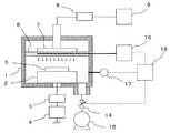
本発明の第4の実施例を、図11ないし図12により説明する。図11は、プラズマ処理装置の概略構成を示す縦断面図である。図11において、図3と同一符号は同一部材を示し、説明を省略する。図11において図3と異なる点は、プラズマ着火検出器19と、バイアス整合器3およびバイアス電源4を制御するための制御装置20を備えていることである。 A fourth embodiment of the present invention will be described with reference to FIGS. FIG. 11 is a longitudinal sectional view showing a schematic configuration of the plasma processing apparatus. In FIG. 11, the same reference numerals as those in FIG. 11 differs from FIG. 3 in that a
予めプラズマ処理条件に応じて、バイアス電力の反射波を低減できるバイアス整合器3の設定を制御装置20により記憶しておく。プラズマ着火前に制御装置20は記憶しておいた設定値をバイアス整合器3に設定し、プラズマを発生する。プラズマ着火検出器19による着火検出と同時に制御装置20はバイアス電源4よりバイアス電力を出力させる。予めバイアス整合器がプラズマ着火後のインピーダンスに応じて設定されているため、バイアス電力印加直後から反射波は抑制され、被処理基板5に速やかにバイアス電位が印加される。 The setting of the
被処理基板にプラズマ着火直後からバイアス電位を印加する効果を、図12を用いて説明する。着火直後のプラズマは、不安定でシースの形成が不十分である。そのため、図12に示すように、着火直後に異物が被処理基板付近に到達すると、シースが異物をプラズマ中に閉じ込める効果も充分でなく、被処理基板に異物が付着する可能性が高い。しかし被処理基板にバイアス電位が印加されていると、シース中の電子が排除され、シースが厚くなることが知られている。シースとプラズマの界面に異物は捕獲されるため、シースを厚くすることで被処理基板から離れた位置に異物が捕獲され、被処理基板への付着を抑制することができる。 The effect of applying a bias potential to the substrate to be processed immediately after plasma ignition will be described with reference to FIG. The plasma immediately after ignition is unstable and the formation of the sheath is insufficient. For this reason, as shown in FIG. 12, when the foreign matter reaches the vicinity of the substrate to be processed immediately after ignition, the sheath does not have a sufficient effect of trapping the foreign matter in the plasma, and there is a high possibility that the foreign matter adheres to the substrate to be processed. However, it is known that when a bias potential is applied to the substrate to be processed, electrons in the sheath are eliminated and the sheath becomes thick. Since the foreign matter is captured at the interface between the sheath and the plasma, by increasing the thickness of the sheath, the foreign matter is captured at a position away from the target substrate, and adhesion to the target substrate can be suppressed.
本発明の第4の実施例を、図13により説明する。図13は、第4の実施例に係るプラズマ処理装置の概略構成を示す縦断面図である。図13において、図3と同一符号は同一部材を示し、説明を省略する。図13において図3と異なる点は、制御装置21が高周波電源9および整合器8、バイアス電源4およびバイアス整合器3をそれぞれ制御する点である。プラズマ着火するために高周波電力を処理室に投入するが、高周波電力の投入と同時にバイアス電源4より整合器3、基板電極2を介して被処理基板5にバイアス電力を投入する点である。バイアス整合器3および整合器8の初期設定を実施例1、実施例4と同様に電力投入初期から整合が取れるように設定しておくことが望ましいが、必ずしも必須ではない。高周波電力とバイアス電力を同時に印加することで実施例4と同様にプラズマプラズマ着火直後のシース形成が不十分な時にバイアス電位がシースに加わることで、異物の被処理基板への落下をより強力に防止することができる。 A fourth embodiment of the present invention will be described with reference to FIG. FIG. 13 is a longitudinal sectional view showing a schematic configuration of a plasma processing apparatus according to the fourth embodiment. In FIG. 13, the same reference numerals as those in FIG. 13 differs from FIG. 3 in that the
1…処理室、2…基板電極、3…整合器、4…高周波バイアス電源、5…被処理基板、6…シャワープレート、7…電極、8…整合器、9…高周波電源、10…制御装置、11…磁場発生装置、12…磁場発生用電源、13…制御装置、14…圧力調整弁、15…真空排気装置、16…ガス供給装置、17…圧力センサ、18…制御装置、19…プラズマモニタ、20…制御装置、21…制御装置。 DESCRIPTION OF
Claims (7)
Translated fromJapanese前記プラズマ処理室に処理ガスを供給するガス供給装置と、
前記プラズマ処理室に整合器を介してプラズマを生成するための高周波電力を供給する高周波電源と、
予め取得されたプラズマが着火するまでの前記整合器の設定値の時系列データを基にプラズマが着火する前の時刻における前記整合器の設定値を保存し、前記被処理基板の前記プラズマ処理を実行する時、前記整合器の初期設定値を前記保存された設定値とする制御を行う制御装置とを備え、
前記プラズマが着火する前の時刻を前記プラズマが着火する時刻より前記高周波電力の供給によって発生した異物が前記被処理基板に到達する時間だけ前の時刻から前記プラズマが着火する時刻までの間の時刻または、前記プラズマが着火する時刻より前記高周波電力の供給によって発生した異物が前記被処理基板に到達する時間からプラズマが安定するのに要する時間を減じた時間だけ前の時刻から前記プラズマが着火する時刻までの間の時刻とすることによって、前記高周波電力の供給により発生した異物が前記被処理基板に到達するまでに前記プラズマを着火させることを特徴とするプラズマ処理装置。In a plasma processing apparatus for plasma processing a substrate to be processed in a plasma processing chamber,
A gas supply device for supplying a processing gas to the plasma processing chamber;
A high-frequency power source for supplying high-frequency power for generating plasma to the plasma processing chamber via a matching unit;
The set value of the matching unit at a time before the plasma is ignited based on the time series data of the set value of the matching unit until the plasma is ignited in advance, and the plasma processing of the substrate to be processed is performed. A control device that performs control to perform the initial setting value of the matching unit as the stored setting value when executing,
Time between the time earlier by time foreign matter generated reaches the substrate to be treated by the supply of the previous time themorethe time that the plasma is ignited frequency power the plasma is igniteduntil the time the plasma is ignited Alternatively, theplasma is ignited from the timebefore the time when the foreign matter generated by supplying the high-frequency power reaches the substrate to be processed is less than the time required for the plasma to be stabilizedfrom the time when the plasma is ignited. A plasma processing apparatus characterizedin that the plasma is ignited until the foreign matter generated by the supply of the high-frequency power reaches the substrate to be processed by settingthe timebetween the time.
前記プラズマ処理室に処理ガスを供給するガス供給装置と、
前記プラズマ処理室に整合器を介してプラズマを生成するための高周波電力を供給する高周波電源と
前記プラズマ処理室に電子サイクロトロン共鳴現象を用いた磁場を発生させる磁場発生用電源と、
前記被処理基板の前記プラズマ処理を実行する時、プラズマが着火する前に前記電子サイクロトロン共鳴現象を用いた磁場が予め定められた前記プラズマの着火に最適な磁場の設定値に調整されるように前記磁場発生用電源を制御する制御装置とを備え、
前記高周波電力の供給とともに前記制御装置により、前記プラズマの着火が容易となる磁場の設定を行うことによって、前記高周波電力の供給により発生した異物が前記被処理基板に到達するまでに前記プラズマを着火させることを特徴とするプラズマ処理装置。In a plasma processing apparatus for plasma processing a substrate to be processed in a plasma processing chamber,
A gas supply device for supplying a processing gas to the plasma processing chamber;
A high-frequency power source for supplying high-frequency power for generating plasma to the plasma processing chamber via a matching unit; a magnetic field generating power source for generating a magnetic fieldusing an electron cyclotron resonance phenomenon in the plasma processing chamber;
When performing the plasma treatment of the substrate to be treated, so thatthe electron cyclotron resonance phenomenon magnetic fieldwithis adjusted to the optimum magnetic field settings to ignition of thepredetermined said plasmabefore the plasma is ignited A control device for controlling the magnetic field generating power supply,
By setting the magnetic field that facilitates the ignition of the plasma by the control device together with the supply of the high-frequency power, the foreign matter generated by the supply of the high-frequency power is ignited until the foreign substance reaches the substrate to be processed. the plasma processingapparatus characterized bycausing.
前記プラズマ処理室に処理ガスを供給するガス供給装置と、
前記プラズマ処理室に整合器を介してプラズマを生成するための高周波電力を供給する高周波電源と、
前記プラズマ処理室内の圧力を調整する圧力調整弁と、
前記被処理基板の前記プラズマ処理を実行する時、プラズマが着火する前の前記プラズマ処理室内の圧力が前記プラズマ処理時の所定の圧力より高くなるように前記圧力調整弁を制御する制御装置とを備え、
前記制御装置により、前記高周波電力の供給よりも前に前記プラズマ処理室内の圧力が前記プラズマ処理時の所定の圧力より高くなるように前記圧力調整弁を制御し、前記プラズマ処理室内のガス圧力が高く設定された状態で前記高周波電力を供給することによって、前記高周波電力の供給により発生した異物が前記被処理基板に到達するまでに前記プラズマを着火させることを特徴とするプラズマ処理装置。In a plasma processing apparatus for plasma processing a substrate to be processed in a plasma processing chamber,
A gas supply device for supplying a processing gas to the plasma processing chamber;
A high-frequency power source for supplying high-frequency power for generating plasma to the plasma processing chamber via a matching unit;
A pressure regulating valve for regulating the pressure in the plasma processing chamber;
When performing the plasma treatment of the substrate to be processed, a controller for controlling thepre-Symbol plasma treatment the pressure adjusting valve so that the pressure becomes higher than a predetermined pressure during the plasma treatment chamberprior to the plasma is ignited With
Thecontrol device controls the pressure regulating valve so that the pressure in the plasma processing chamber is higher than a predetermined pressure during the plasma processing before the supply of the high-frequency power, and the gas pressure in the plasma processing chamber is A plasma processing apparatus characterizedin that, by supplying the high frequency power in a high setting state, the plasma is ignited until foreign matter generated by the supply of the high frequency power reaches the substrate to be processed .
前記プラズマ処理室内に設けられ、前記被処理基板を載置する被処理基板電極に高周波バイアス電力を供給する高周波バイアス電源とを備え、
前記制御装置は、前記高周波電力が供給されるとともに前記高周波バイアス電力を供給するように前記高周波電源および前記高周波バイアス電源を制御することを特徴とするプラズマ処理装置。The plasma processing apparatus according to claim 1,
A high frequency bias power source that is provided in the plasma processing chamber and supplies a high frequency bias power to a substrate electrode to be processed on which the substrate to be processed is placed;
The control apparatus controls the high-frequency power source and the high-frequency bias power source so that the high-frequency power is supplied and the high-frequency bias power is supplied.
前記プラズマ処理室に処理ガスを供給するガス供給装置と、
前記プラズマ処理室に整合器を介してプラズマを生成するための高周波電力を供給する高周波電源とを備えるプラズマ処理装置を用いて前記被処理基板をプラズマ処理するプラズマ処理方法において、
予め取得されたプラズマが着火するまでの前記整合器の設定値の時系列データを基にプラズマが着火する前の時刻における前記整合器の設定値を保存し、前記被処理基板の前記プラズマ処理を実行する時、前記整合器の初期設定値を前記保存された設定値とする制御を行い、
前記プラズマが着火する前の時刻を前記プラズマが着火する時刻より前記高周波電力の供給によって発生した異物が前記被処理基板に到達する時間だけ前の時刻から前記プラズマが着火する時刻までの間の時刻または、前記プラズマが着火する時刻より前記高周波電力の供給によって発生した異物が前記被処理基板に到達する時間からプラズマが安定するのに要する時間を減じた時間だけ前の時刻から前記プラズマが着火する時刻までの間の時刻とすることによって、前記高周波電力の供給により発生した異物が前記被処理基板に到達するまでに前記プラズマを着火させることを特徴とするであることを特徴とするプラズマ処理方法。A plasma processing chamber for plasma processing a substrate to be processed;
A gas supply device for supplying a processing gas to the plasma processing chamber;
In the plasma processing method for plasma processing the substrate to be processed using a plasma processing apparatus comprising a high-frequency power source for supplying high-frequency power for generating plasma to the plasma processing chamber via a matching unit,
The set value of the matching unit at a time before the plasma is ignited based on the time series data of the set value of the matching unit until the plasma is ignited in advance, and the plasma processing of the substrate to be processed is performed. When executing, the initial setting value of the matching device is controlled to be the stored setting value,
Time between the time earlier by time foreign matter generated reaches the substrate to be treated by the supply of the previous time themorethe time that the plasma is ignited frequency power the plasma is igniteduntil the time the plasma is ignited Alternatively, theplasma is ignited from the timebefore the time when the foreign matter generated by supplying the high-frequency power reaches the substrate to be processed is less than the time required for the plasma to be stabilizedfrom the time when the plasma is ignited. The plasma processing method is characterizedin that the plasma is ignited before the foreign matter generated by the supply of the high-frequency power reaches the substrate to be processed by settingthe timebetween the time. .
前記プラズマ処理室に処理ガスを供給するガス供給装置と、
前記プラズマ処理室に整合器を介してプラズマを生成するための高周波電力を供給する高周波電源と
前記プラズマ処理室に電子サイクロトロン共鳴現象を用いた磁場を発生させる磁場発生用電源とを備えるプラズマ処理装置を用いて前記被処理基板をプラズマ処理するプラズマ処理方法において、
前記被処理基板の前記プラズマ処理を実行する時、プラズマが着火する前に前記電子サイクロトロン共鳴現象を用いた磁場が予め定められた前記プラズマの着火に最適な磁場の設定値に調整されるように前記磁場発生用電源を制御し、
前記高周波電力の供給とともに前記制御装置により、前記プラズマの着火が容易となる磁場の設定を行うことによって、前記高周波電力の供給により発生した異物が前記被処理基板に到達するまでに前記プラズマを着火させることを特徴とするプラズマ処理方法。A plasma processing chamber for plasma processing a substrate to be processed;
A gas supply device for supplying a processing gas to the plasma processing chamber;
A plasma processing apparatus comprising: a high-frequency power source that supplies high-frequency power for generating plasma to the plasma processing chamber via a matching unit; and a magnetic field generation power source that generates a magnetic fieldusing an electron cyclotron resonance phenomenon in the plasma processing chamber In the plasma processing method of plasma processing the substrate to be processed using
Wherein when performing the plasma treatment of the substrate to be processed, to so thatis adjusted totheoptimum magnetic field settings to ignition of theelectron cyclotron resonance theplasma phenomenon magnetic fieldwith thepredeterminedbefore the plasma is ignited Controlling the power source for generating the magnetic field,
By setting the magnetic field that facilitates the ignition of the plasma by the control device together with the supply of the high-frequency power, the foreign matter generated by the supply of the high-frequency power is ignited until the foreign substance reaches the substrate to be processed. the plasma processing method characterized inthat cause.
前記プラズマ処理室に処理ガスを供給するガス供給装置と、
前記プラズマ処理室に整合器を介してプラズマを生成するための高周波電力を供給する高周波電源と
前記プラズマ処理室内の圧力を調整する圧力調整弁とを備えるプラズマ処理装置を用いて前記被処理基板をプラズマ処理するプラズマ処理方法において、
前記被処理基板の前記プラズマ処理を実行する時、プラズマが着火する前の前記プラズマ処理室内の圧力が前記プラズマ処理時の所定の圧力より高くなるように前記圧力調整弁を制御し、
前記制御装置により、前記高周波電力の供給よりも前に前記プラズマ処理室内の圧力が前記プラズマ処理時の所定の圧力より高くなるように前記圧力調整弁を制御し、前記プラズマ処理室内のガス圧力が高く設定された状態で前記高周波電力を供給することによって、前記高周波電力の供給により発生した異物が前記被処理基板に到達するまでに前記プラズマを着火させることを特徴とするプラズマ処理方法。A plasma processing chamber for plasma processing a substrate to be processed;
A gas supply device for supplying a processing gas to the plasma processing chamber;
The substrate to be processed using a plasma processing apparatus comprising: a high-frequency power source for supplying high-frequency power for generating plasma to the plasma processing chamber via a matching unit; and a pressure adjusting valve for adjusting a pressure in the plasma processing chamber. In the plasma processing method for plasma processing,
Wherein when performing the plasma treatment of the substrate to be processed, and controls thepre-Symbol plasma treatment the pressure adjusting valve so that the pressure becomes higher than a predetermined pressure during the plasma treatment chamberprior to the plasma is ignited,
Thecontrol device controls the pressure regulating valve so that the pressure in the plasma processing chamber is higher than a predetermined pressure during the plasma processing before the supply of the high-frequency power, and the gas pressure in the plasma processing chamber is A plasma processing methodcomprising: igniting the plasma until foreign matter generated by the supply of the high-frequency power reaches the substrate to be processed by supplying the high-frequency power in a high setting state .
Priority Applications (1)
| Application Number | Priority Date | Filing Date | Title |
|---|---|---|---|
| JP2006235103AJP4943780B2 (en) | 2006-08-31 | 2006-08-31 | Plasma processing apparatus and plasma processing method |
Applications Claiming Priority (1)
| Application Number | Priority Date | Filing Date | Title |
|---|---|---|---|
| JP2006235103AJP4943780B2 (en) | 2006-08-31 | 2006-08-31 | Plasma processing apparatus and plasma processing method |
Publications (2)
| Publication Number | Publication Date |
|---|---|
| JP2008060304A JP2008060304A (en) | 2008-03-13 |
| JP4943780B2true JP4943780B2 (en) | 2012-05-30 |
Family
ID=39242702
Family Applications (1)
| Application Number | Title | Priority Date | Filing Date |
|---|---|---|---|
| JP2006235103AExpired - Fee RelatedJP4943780B2 (en) | 2006-08-31 | 2006-08-31 | Plasma processing apparatus and plasma processing method |
Country Status (1)
| Country | Link |
|---|---|
| JP (1) | JP4943780B2 (en) |
Families Citing this family (389)
| Publication number | Priority date | Publication date | Assignee | Title |
|---|---|---|---|---|
| US10378106B2 (en) | 2008-11-14 | 2019-08-13 | Asm Ip Holding B.V. | Method of forming insulation film by modified PEALD |
| US9394608B2 (en) | 2009-04-06 | 2016-07-19 | Asm America, Inc. | Semiconductor processing reactor and components thereof |
| US8802201B2 (en) | 2009-08-14 | 2014-08-12 | Asm America, Inc. | Systems and methods for thin-film deposition of metal oxides using excited nitrogen-oxygen species |
| JP5781286B2 (en)* | 2010-09-30 | 2015-09-16 | 芝浦メカトロニクス株式会社 | Plasma processing method and plasma processing apparatus |
| US9312155B2 (en) | 2011-06-06 | 2016-04-12 | Asm Japan K.K. | High-throughput semiconductor-processing apparatus equipped with multiple dual-chamber modules |
| US9793148B2 (en) | 2011-06-22 | 2017-10-17 | Asm Japan K.K. | Method for positioning wafers in multiple wafer transport |
| US10364496B2 (en) | 2011-06-27 | 2019-07-30 | Asm Ip Holding B.V. | Dual section module having shared and unshared mass flow controllers |
| US10854498B2 (en) | 2011-07-15 | 2020-12-01 | Asm Ip Holding B.V. | Wafer-supporting device and method for producing same |
| US20130023129A1 (en) | 2011-07-20 | 2013-01-24 | Asm America, Inc. | Pressure transmitter for a semiconductor processing environment |
| US9017481B1 (en) | 2011-10-28 | 2015-04-28 | Asm America, Inc. | Process feed management for semiconductor substrate processing |
| US8946830B2 (en) | 2012-04-04 | 2015-02-03 | Asm Ip Holdings B.V. | Metal oxide protective layer for a semiconductor device |
| US9558931B2 (en) | 2012-07-27 | 2017-01-31 | Asm Ip Holding B.V. | System and method for gas-phase sulfur passivation of a semiconductor surface |
| US9659799B2 (en) | 2012-08-28 | 2017-05-23 | Asm Ip Holding B.V. | Systems and methods for dynamic semiconductor process scheduling |
| US8742668B2 (en) | 2012-09-05 | 2014-06-03 | Asm Ip Holdings B.V. | Method for stabilizing plasma ignition |
| US9021985B2 (en) | 2012-09-12 | 2015-05-05 | Asm Ip Holdings B.V. | Process gas management for an inductively-coupled plasma deposition reactor |
| US9324811B2 (en) | 2012-09-26 | 2016-04-26 | Asm Ip Holding B.V. | Structures and devices including a tensile-stressed silicon arsenic layer and methods of forming same |
| US10714315B2 (en) | 2012-10-12 | 2020-07-14 | Asm Ip Holdings B.V. | Semiconductor reaction chamber showerhead |
| US9640416B2 (en) | 2012-12-26 | 2017-05-02 | Asm Ip Holding B.V. | Single-and dual-chamber module-attachable wafer-handling chamber |
| US20160376700A1 (en) | 2013-02-01 | 2016-12-29 | Asm Ip Holding B.V. | System for treatment of deposition reactor |
| JP2014157758A (en)* | 2013-02-18 | 2014-08-28 | Sumitomo Heavy Ind Ltd | Microwave ion source and method of starting the same |
| US9589770B2 (en) | 2013-03-08 | 2017-03-07 | Asm Ip Holding B.V. | Method and systems for in-situ formation of intermediate reactive species |
| US9484191B2 (en) | 2013-03-08 | 2016-11-01 | Asm Ip Holding B.V. | Pulsed remote plasma method and system |
| US8993054B2 (en) | 2013-07-12 | 2015-03-31 | Asm Ip Holding B.V. | Method and system to reduce outgassing in a reaction chamber |
| US9018111B2 (en) | 2013-07-22 | 2015-04-28 | Asm Ip Holding B.V. | Semiconductor reaction chamber with plasma capabilities |
| US9793115B2 (en) | 2013-08-14 | 2017-10-17 | Asm Ip Holding B.V. | Structures and devices including germanium-tin films and methods of forming same |
| US9240412B2 (en) | 2013-09-27 | 2016-01-19 | Asm Ip Holding B.V. | Semiconductor structure and device and methods of forming same using selective epitaxial process |
| US9556516B2 (en) | 2013-10-09 | 2017-01-31 | ASM IP Holding B.V | Method for forming Ti-containing film by PEALD using TDMAT or TDEAT |
| US10179947B2 (en) | 2013-11-26 | 2019-01-15 | Asm Ip Holding B.V. | Method for forming conformal nitrided, oxidized, or carbonized dielectric film by atomic layer deposition |
| US10683571B2 (en) | 2014-02-25 | 2020-06-16 | Asm Ip Holding B.V. | Gas supply manifold and method of supplying gases to chamber using same |
| US9447498B2 (en) | 2014-03-18 | 2016-09-20 | Asm Ip Holding B.V. | Method for performing uniform processing in gas system-sharing multiple reaction chambers |
| US10167557B2 (en) | 2014-03-18 | 2019-01-01 | Asm Ip Holding B.V. | Gas distribution system, reactor including the system, and methods of using the same |
| US11015245B2 (en) | 2014-03-19 | 2021-05-25 | Asm Ip Holding B.V. | Gas-phase reactor and system having exhaust plenum and components thereof |
| US9404587B2 (en) | 2014-04-24 | 2016-08-02 | ASM IP Holding B.V | Lockout tagout for semiconductor vacuum valve |
| US9530626B2 (en)* | 2014-07-25 | 2016-12-27 | Tokyo Electron Limited | Method and apparatus for ESC charge control for wafer clamping |
| US10858737B2 (en) | 2014-07-28 | 2020-12-08 | Asm Ip Holding B.V. | Showerhead assembly and components thereof |
| US9543180B2 (en) | 2014-08-01 | 2017-01-10 | Asm Ip Holding B.V. | Apparatus and method for transporting wafers between wafer carrier and process tool under vacuum |
| US9890456B2 (en) | 2014-08-21 | 2018-02-13 | Asm Ip Holding B.V. | Method and system for in situ formation of gas-phase compounds |
| US9657845B2 (en) | 2014-10-07 | 2017-05-23 | Asm Ip Holding B.V. | Variable conductance gas distribution apparatus and method |
| US10941490B2 (en) | 2014-10-07 | 2021-03-09 | Asm Ip Holding B.V. | Multiple temperature range susceptor, assembly, reactor and system including the susceptor, and methods of using the same |
| KR102300403B1 (en) | 2014-11-19 | 2021-09-09 | 에이에스엠 아이피 홀딩 비.브이. | Method of depositing thin film |
| KR102263121B1 (en) | 2014-12-22 | 2021-06-09 | 에이에스엠 아이피 홀딩 비.브이. | Semiconductor device and manufacuring method thereof |
| US9478415B2 (en) | 2015-02-13 | 2016-10-25 | Asm Ip Holding B.V. | Method for forming film having low resistance and shallow junction depth |
| US10529542B2 (en) | 2015-03-11 | 2020-01-07 | Asm Ip Holdings B.V. | Cross-flow reactor and method |
| US10276355B2 (en) | 2015-03-12 | 2019-04-30 | Asm Ip Holding B.V. | Multi-zone reactor, system including the reactor, and method of using the same |
| US10458018B2 (en) | 2015-06-26 | 2019-10-29 | Asm Ip Holding B.V. | Structures including metal carbide material, devices including the structures, and methods of forming same |
| US10600673B2 (en) | 2015-07-07 | 2020-03-24 | Asm Ip Holding B.V. | Magnetic susceptor to baseplate seal |
| US10043661B2 (en) | 2015-07-13 | 2018-08-07 | Asm Ip Holding B.V. | Method for protecting layer by forming hydrocarbon-based extremely thin film |
| US9899291B2 (en) | 2015-07-13 | 2018-02-20 | Asm Ip Holding B.V. | Method for protecting layer by forming hydrocarbon-based extremely thin film |
| US10083836B2 (en) | 2015-07-24 | 2018-09-25 | Asm Ip Holding B.V. | Formation of boron-doped titanium metal films with high work function |
| US10087525B2 (en) | 2015-08-04 | 2018-10-02 | Asm Ip Holding B.V. | Variable gap hard stop design |
| US9647114B2 (en) | 2015-08-14 | 2017-05-09 | Asm Ip Holding B.V. | Methods of forming highly p-type doped germanium tin films and structures and devices including the films |
| US9711345B2 (en) | 2015-08-25 | 2017-07-18 | Asm Ip Holding B.V. | Method for forming aluminum nitride-based film by PEALD |
| US9960072B2 (en) | 2015-09-29 | 2018-05-01 | Asm Ip Holding B.V. | Variable adjustment for precise matching of multiple chamber cavity housings |
| US9909214B2 (en) | 2015-10-15 | 2018-03-06 | Asm Ip Holding B.V. | Method for depositing dielectric film in trenches by PEALD |
| US10211308B2 (en) | 2015-10-21 | 2019-02-19 | Asm Ip Holding B.V. | NbMC layers |
| US10322384B2 (en) | 2015-11-09 | 2019-06-18 | Asm Ip Holding B.V. | Counter flow mixer for process chamber |
| US9455138B1 (en) | 2015-11-10 | 2016-09-27 | Asm Ip Holding B.V. | Method for forming dielectric film in trenches by PEALD using H-containing gas |
| US9607837B1 (en) | 2015-12-21 | 2017-03-28 | Asm Ip Holding B.V. | Method for forming silicon oxide cap layer for solid state diffusion process |
| US9627221B1 (en) | 2015-12-28 | 2017-04-18 | Asm Ip Holding B.V. | Continuous process incorporating atomic layer etching |
| US9735024B2 (en) | 2015-12-28 | 2017-08-15 | Asm Ip Holding B.V. | Method of atomic layer etching using functional group-containing fluorocarbon |
| US11139308B2 (en) | 2015-12-29 | 2021-10-05 | Asm Ip Holding B.V. | Atomic layer deposition of III-V compounds to form V-NAND devices |
| US10468251B2 (en) | 2016-02-19 | 2019-11-05 | Asm Ip Holding B.V. | Method for forming spacers using silicon nitride film for spacer-defined multiple patterning |
| US10529554B2 (en) | 2016-02-19 | 2020-01-07 | Asm Ip Holding B.V. | Method for forming silicon nitride film selectively on sidewalls or flat surfaces of trenches |
| US9754779B1 (en) | 2016-02-19 | 2017-09-05 | Asm Ip Holding B.V. | Method for forming silicon nitride film selectively on sidewalls or flat surfaces of trenches |
| US10501866B2 (en) | 2016-03-09 | 2019-12-10 | Asm Ip Holding B.V. | Gas distribution apparatus for improved film uniformity in an epitaxial system |
| US10343920B2 (en) | 2016-03-18 | 2019-07-09 | Asm Ip Holding B.V. | Aligned carbon nanotubes |
| US9892913B2 (en) | 2016-03-24 | 2018-02-13 | Asm Ip Holding B.V. | Radial and thickness control via biased multi-port injection settings |
| US10087522B2 (en) | 2016-04-21 | 2018-10-02 | Asm Ip Holding B.V. | Deposition of metal borides |
| US10865475B2 (en) | 2016-04-21 | 2020-12-15 | Asm Ip Holding B.V. | Deposition of metal borides and silicides |
| US10190213B2 (en) | 2016-04-21 | 2019-01-29 | Asm Ip Holding B.V. | Deposition of metal borides |
| US10032628B2 (en) | 2016-05-02 | 2018-07-24 | Asm Ip Holding B.V. | Source/drain performance through conformal solid state doping |
| US10367080B2 (en) | 2016-05-02 | 2019-07-30 | Asm Ip Holding B.V. | Method of forming a germanium oxynitride film |
| KR102592471B1 (en) | 2016-05-17 | 2023-10-20 | 에이에스엠 아이피 홀딩 비.브이. | Method of forming metal interconnection and method of fabricating semiconductor device using the same |
| US10388509B2 (en) | 2016-06-28 | 2019-08-20 | Asm Ip Holding B.V. | Formation of epitaxial layers via dislocation filtering |
| US9859151B1 (en) | 2016-07-08 | 2018-01-02 | Asm Ip Holding B.V. | Selective film deposition method to form air gaps |
| US10612137B2 (en) | 2016-07-08 | 2020-04-07 | Asm Ip Holdings B.V. | Organic reactants for atomic layer deposition |
| US9793135B1 (en) | 2016-07-14 | 2017-10-17 | ASM IP Holding B.V | Method of cyclic dry etching using etchant film |
| US10714385B2 (en) | 2016-07-19 | 2020-07-14 | Asm Ip Holding B.V. | Selective deposition of tungsten |
| KR102354490B1 (en) | 2016-07-27 | 2022-01-21 | 에이에스엠 아이피 홀딩 비.브이. | Method of processing a substrate |
| US10395919B2 (en) | 2016-07-28 | 2019-08-27 | Asm Ip Holding B.V. | Method and apparatus for filling a gap |
| US10177025B2 (en) | 2016-07-28 | 2019-01-08 | Asm Ip Holding B.V. | Method and apparatus for filling a gap |
| US9812320B1 (en) | 2016-07-28 | 2017-11-07 | Asm Ip Holding B.V. | Method and apparatus for filling a gap |
| US9887082B1 (en) | 2016-07-28 | 2018-02-06 | Asm Ip Holding B.V. | Method and apparatus for filling a gap |
| KR102532607B1 (en) | 2016-07-28 | 2023-05-15 | 에이에스엠 아이피 홀딩 비.브이. | Substrate processing apparatus and method of operating the same |
| US10090316B2 (en) | 2016-09-01 | 2018-10-02 | Asm Ip Holding B.V. | 3D stacked multilayer semiconductor memory using doped select transistor channel |
| US10410943B2 (en) | 2016-10-13 | 2019-09-10 | Asm Ip Holding B.V. | Method for passivating a surface of a semiconductor and related systems |
| US10643826B2 (en) | 2016-10-26 | 2020-05-05 | Asm Ip Holdings B.V. | Methods for thermally calibrating reaction chambers |
| US11532757B2 (en) | 2016-10-27 | 2022-12-20 | Asm Ip Holding B.V. | Deposition of charge trapping layers |
| US10229833B2 (en) | 2016-11-01 | 2019-03-12 | Asm Ip Holding B.V. | Methods for forming a transition metal nitride film on a substrate by atomic layer deposition and related semiconductor device structures |
| US10643904B2 (en) | 2016-11-01 | 2020-05-05 | Asm Ip Holdings B.V. | Methods for forming a semiconductor device and related semiconductor device structures |
| US10435790B2 (en) | 2016-11-01 | 2019-10-08 | Asm Ip Holding B.V. | Method of subatmospheric plasma-enhanced ALD using capacitively coupled electrodes with narrow gap |
| US10714350B2 (en) | 2016-11-01 | 2020-07-14 | ASM IP Holdings, B.V. | Methods for forming a transition metal niobium nitride film on a substrate by atomic layer deposition and related semiconductor device structures |
| US10134757B2 (en) | 2016-11-07 | 2018-11-20 | Asm Ip Holding B.V. | Method of processing a substrate and a device manufactured by using the method |
| KR102546317B1 (en) | 2016-11-15 | 2023-06-21 | 에이에스엠 아이피 홀딩 비.브이. | Gas supply unit and substrate processing apparatus including the same |
| US10340135B2 (en) | 2016-11-28 | 2019-07-02 | Asm Ip Holding B.V. | Method of topologically restricted plasma-enhanced cyclic deposition of silicon or metal nitride |
| KR102762543B1 (en) | 2016-12-14 | 2025-02-05 | 에이에스엠 아이피 홀딩 비.브이. | Substrate processing apparatus |
| US11581186B2 (en) | 2016-12-15 | 2023-02-14 | Asm Ip Holding B.V. | Sequential infiltration synthesis apparatus |
| US9916980B1 (en) | 2016-12-15 | 2018-03-13 | Asm Ip Holding B.V. | Method of forming a structure on a substrate |
| US11447861B2 (en) | 2016-12-15 | 2022-09-20 | Asm Ip Holding B.V. | Sequential infiltration synthesis apparatus and a method of forming a patterned structure |
| KR102700194B1 (en) | 2016-12-19 | 2024-08-28 | 에이에스엠 아이피 홀딩 비.브이. | Substrate processing apparatus |
| US10269558B2 (en) | 2016-12-22 | 2019-04-23 | Asm Ip Holding B.V. | Method of forming a structure on a substrate |
| US10867788B2 (en) | 2016-12-28 | 2020-12-15 | Asm Ip Holding B.V. | Method of forming a structure on a substrate |
| US11390950B2 (en) | 2017-01-10 | 2022-07-19 | Asm Ip Holding B.V. | Reactor system and method to reduce residue buildup during a film deposition process |
| JP6242513B2 (en)* | 2017-01-11 | 2017-12-06 | 住友重機械工業株式会社 | Microwave ion source and starting method thereof |
| US10655221B2 (en) | 2017-02-09 | 2020-05-19 | Asm Ip Holding B.V. | Method for depositing oxide film by thermal ALD and PEALD |
| US10468261B2 (en) | 2017-02-15 | 2019-11-05 | Asm Ip Holding B.V. | Methods for forming a metallic film on a substrate by cyclical deposition and related semiconductor device structures |
| US10529563B2 (en) | 2017-03-29 | 2020-01-07 | Asm Ip Holdings B.V. | Method for forming doped metal oxide films on a substrate by cyclical deposition and related semiconductor device structures |
| US10283353B2 (en) | 2017-03-29 | 2019-05-07 | Asm Ip Holding B.V. | Method of reforming insulating film deposited on substrate with recess pattern |
| US10103040B1 (en) | 2017-03-31 | 2018-10-16 | Asm Ip Holding B.V. | Apparatus and method for manufacturing a semiconductor device |
| USD830981S1 (en) | 2017-04-07 | 2018-10-16 | Asm Ip Holding B.V. | Susceptor for semiconductor substrate processing apparatus |
| KR102457289B1 (en) | 2017-04-25 | 2022-10-21 | 에이에스엠 아이피 홀딩 비.브이. | Method for depositing a thin film and manufacturing a semiconductor device |
| US10770286B2 (en) | 2017-05-08 | 2020-09-08 | Asm Ip Holdings B.V. | Methods for selectively forming a silicon nitride film on a substrate and related semiconductor device structures |
| US10892156B2 (en) | 2017-05-08 | 2021-01-12 | Asm Ip Holding B.V. | Methods for forming a silicon nitride film on a substrate and related semiconductor device structures |
| US10446393B2 (en) | 2017-05-08 | 2019-10-15 | Asm Ip Holding B.V. | Methods for forming silicon-containing epitaxial layers and related semiconductor device structures |
| US10504742B2 (en) | 2017-05-31 | 2019-12-10 | Asm Ip Holding B.V. | Method of atomic layer etching using hydrogen plasma |
| US10886123B2 (en) | 2017-06-02 | 2021-01-05 | Asm Ip Holding B.V. | Methods for forming low temperature semiconductor layers and related semiconductor device structures |
| US12040200B2 (en) | 2017-06-20 | 2024-07-16 | Asm Ip Holding B.V. | Semiconductor processing apparatus and methods for calibrating a semiconductor processing apparatus |
| US11306395B2 (en) | 2017-06-28 | 2022-04-19 | Asm Ip Holding B.V. | Methods for depositing a transition metal nitride film on a substrate by atomic layer deposition and related deposition apparatus |
| US10685834B2 (en) | 2017-07-05 | 2020-06-16 | Asm Ip Holdings B.V. | Methods for forming a silicon germanium tin layer and related semiconductor device structures |
| KR20190009245A (en) | 2017-07-18 | 2019-01-28 | 에이에스엠 아이피 홀딩 비.브이. | Methods for forming a semiconductor device structure and related semiconductor device structures |
| US11374112B2 (en) | 2017-07-19 | 2022-06-28 | Asm Ip Holding B.V. | Method for depositing a group IV semiconductor and related semiconductor device structures |
| US11018002B2 (en) | 2017-07-19 | 2021-05-25 | Asm Ip Holding B.V. | Method for selectively depositing a Group IV semiconductor and related semiconductor device structures |
| US10541333B2 (en) | 2017-07-19 | 2020-01-21 | Asm Ip Holding B.V. | Method for depositing a group IV semiconductor and related semiconductor device structures |
| US10312055B2 (en) | 2017-07-26 | 2019-06-04 | Asm Ip Holding B.V. | Method of depositing film by PEALD using negative bias |
| US10605530B2 (en) | 2017-07-26 | 2020-03-31 | Asm Ip Holding B.V. | Assembly of a liner and a flange for a vertical furnace as well as the liner and the vertical furnace |
| US10590535B2 (en) | 2017-07-26 | 2020-03-17 | Asm Ip Holdings B.V. | Chemical treatment, deposition and/or infiltration apparatus and method for using the same |
| TWI815813B (en) | 2017-08-04 | 2023-09-21 | 荷蘭商Asm智慧財產控股公司 | Showerhead assembly for distributing a gas within a reaction chamber |
| US10770336B2 (en) | 2017-08-08 | 2020-09-08 | Asm Ip Holding B.V. | Substrate lift mechanism and reactor including same |
| US10692741B2 (en) | 2017-08-08 | 2020-06-23 | Asm Ip Holdings B.V. | Radiation shield |
| US11139191B2 (en) | 2017-08-09 | 2021-10-05 | Asm Ip Holding B.V. | Storage apparatus for storing cassettes for substrates and processing apparatus equipped therewith |
| US10249524B2 (en) | 2017-08-09 | 2019-04-02 | Asm Ip Holding B.V. | Cassette holder assembly for a substrate cassette and holding member for use in such assembly |
| US11769682B2 (en) | 2017-08-09 | 2023-09-26 | Asm Ip Holding B.V. | Storage apparatus for storing cassettes for substrates and processing apparatus equipped therewith |
| US10236177B1 (en) | 2017-08-22 | 2019-03-19 | ASM IP Holding B.V.. | Methods for depositing a doped germanium tin semiconductor and related semiconductor device structures |
| USD900036S1 (en) | 2017-08-24 | 2020-10-27 | Asm Ip Holding B.V. | Heater electrical connector and adapter |
| US11830730B2 (en) | 2017-08-29 | 2023-11-28 | Asm Ip Holding B.V. | Layer forming method and apparatus |
| US11056344B2 (en) | 2017-08-30 | 2021-07-06 | Asm Ip Holding B.V. | Layer forming method |
| US11295980B2 (en) | 2017-08-30 | 2022-04-05 | Asm Ip Holding B.V. | Methods for depositing a molybdenum metal film over a dielectric surface of a substrate by a cyclical deposition process and related semiconductor device structures |
| KR102491945B1 (en) | 2017-08-30 | 2023-01-26 | 에이에스엠 아이피 홀딩 비.브이. | Substrate processing apparatus |
| KR102401446B1 (en) | 2017-08-31 | 2022-05-24 | 에이에스엠 아이피 홀딩 비.브이. | Substrate processing apparatus |
| US10607895B2 (en) | 2017-09-18 | 2020-03-31 | Asm Ip Holdings B.V. | Method for forming a semiconductor device structure comprising a gate fill metal |
| KR102630301B1 (en) | 2017-09-21 | 2024-01-29 | 에이에스엠 아이피 홀딩 비.브이. | Method of sequential infiltration synthesis treatment of infiltrateable material and structures and devices formed using same |
| US10844484B2 (en) | 2017-09-22 | 2020-11-24 | Asm Ip Holding B.V. | Apparatus for dispensing a vapor phase reactant to a reaction chamber and related methods |
| US10658205B2 (en) | 2017-09-28 | 2020-05-19 | Asm Ip Holdings B.V. | Chemical dispensing apparatus and methods for dispensing a chemical to a reaction chamber |
| US10403504B2 (en) | 2017-10-05 | 2019-09-03 | Asm Ip Holding B.V. | Method for selectively depositing a metallic film on a substrate |
| US10319588B2 (en) | 2017-10-10 | 2019-06-11 | Asm Ip Holding B.V. | Method for depositing a metal chalcogenide on a substrate by cyclical deposition |
| US10923344B2 (en) | 2017-10-30 | 2021-02-16 | Asm Ip Holding B.V. | Methods for forming a semiconductor structure and related semiconductor structures |
| KR102443047B1 (en) | 2017-11-16 | 2022-09-14 | 에이에스엠 아이피 홀딩 비.브이. | Method of processing a substrate and a device manufactured by the same |
| US10910262B2 (en) | 2017-11-16 | 2021-02-02 | Asm Ip Holding B.V. | Method of selectively depositing a capping layer structure on a semiconductor device structure |
| US11022879B2 (en) | 2017-11-24 | 2021-06-01 | Asm Ip Holding B.V. | Method of forming an enhanced unexposed photoresist layer |
| WO2019103613A1 (en) | 2017-11-27 | 2019-05-31 | Asm Ip Holding B.V. | A storage device for storing wafer cassettes for use with a batch furnace |
| CN111344522B (en) | 2017-11-27 | 2022-04-12 | 阿斯莫Ip控股公司 | Including clean mini-environment device |
| US10290508B1 (en) | 2017-12-05 | 2019-05-14 | Asm Ip Holding B.V. | Method for forming vertical spacers for spacer-defined patterning |
| US10872771B2 (en) | 2018-01-16 | 2020-12-22 | Asm Ip Holding B. V. | Method for depositing a material film on a substrate within a reaction chamber by a cyclical deposition process and related device structures |
| TWI799494B (en) | 2018-01-19 | 2023-04-21 | 荷蘭商Asm 智慧財產控股公司 | Deposition method |
| KR102695659B1 (en) | 2018-01-19 | 2024-08-14 | 에이에스엠 아이피 홀딩 비.브이. | Method for depositing a gap filling layer by plasma assisted deposition |
| USD903477S1 (en) | 2018-01-24 | 2020-12-01 | Asm Ip Holdings B.V. | Metal clamp |
| US11018047B2 (en) | 2018-01-25 | 2021-05-25 | Asm Ip Holding B.V. | Hybrid lift pin |
| USD880437S1 (en) | 2018-02-01 | 2020-04-07 | Asm Ip Holding B.V. | Gas supply plate for semiconductor manufacturing apparatus |
| US10535516B2 (en) | 2018-02-01 | 2020-01-14 | Asm Ip Holdings B.V. | Method for depositing a semiconductor structure on a surface of a substrate and related semiconductor structures |
| US11081345B2 (en) | 2018-02-06 | 2021-08-03 | Asm Ip Holding B.V. | Method of post-deposition treatment for silicon oxide film |
| US10896820B2 (en) | 2018-02-14 | 2021-01-19 | Asm Ip Holding B.V. | Method for depositing a ruthenium-containing film on a substrate by a cyclical deposition process |
| WO2019158960A1 (en) | 2018-02-14 | 2019-08-22 | Asm Ip Holding B.V. | A method for depositing a ruthenium-containing film on a substrate by a cyclical deposition process |
| US10731249B2 (en) | 2018-02-15 | 2020-08-04 | Asm Ip Holding B.V. | Method of forming a transition metal containing film on a substrate by a cyclical deposition process, a method for supplying a transition metal halide compound to a reaction chamber, and related vapor deposition apparatus |
| US10658181B2 (en) | 2018-02-20 | 2020-05-19 | Asm Ip Holding B.V. | Method of spacer-defined direct patterning in semiconductor fabrication |
| KR102636427B1 (en) | 2018-02-20 | 2024-02-13 | 에이에스엠 아이피 홀딩 비.브이. | Substrate processing method and apparatus |
| US10975470B2 (en) | 2018-02-23 | 2021-04-13 | Asm Ip Holding B.V. | Apparatus for detecting or monitoring for a chemical precursor in a high temperature environment |
| US11473195B2 (en) | 2018-03-01 | 2022-10-18 | Asm Ip Holding B.V. | Semiconductor processing apparatus and a method for processing a substrate |
| US11629406B2 (en) | 2018-03-09 | 2023-04-18 | Asm Ip Holding B.V. | Semiconductor processing apparatus comprising one or more pyrometers for measuring a temperature of a substrate during transfer of the substrate |
| US11114283B2 (en) | 2018-03-16 | 2021-09-07 | Asm Ip Holding B.V. | Reactor, system including the reactor, and methods of manufacturing and using same |
| KR102646467B1 (en) | 2018-03-27 | 2024-03-11 | 에이에스엠 아이피 홀딩 비.브이. | Method of forming an electrode on a substrate and a semiconductor device structure including an electrode |
| US11088002B2 (en) | 2018-03-29 | 2021-08-10 | Asm Ip Holding B.V. | Substrate rack and a substrate processing system and method |
| US10510536B2 (en) | 2018-03-29 | 2019-12-17 | Asm Ip Holding B.V. | Method of depositing a co-doped polysilicon film on a surface of a substrate within a reaction chamber |
| US11230766B2 (en) | 2018-03-29 | 2022-01-25 | Asm Ip Holding B.V. | Substrate processing apparatus and method |
| KR102501472B1 (en) | 2018-03-30 | 2023-02-20 | 에이에스엠 아이피 홀딩 비.브이. | Substrate processing method |
| KR102600229B1 (en) | 2018-04-09 | 2023-11-10 | 에이에스엠 아이피 홀딩 비.브이. | Substrate supporting device, substrate processing apparatus including the same and substrate processing method |
| TWI811348B (en) | 2018-05-08 | 2023-08-11 | 荷蘭商Asm 智慧財產控股公司 | Methods for depositing an oxide film on a substrate by a cyclical deposition process and related device structures |
| US12025484B2 (en) | 2018-05-08 | 2024-07-02 | Asm Ip Holding B.V. | Thin film forming method |
| US12272527B2 (en) | 2018-05-09 | 2025-04-08 | Asm Ip Holding B.V. | Apparatus for use with hydrogen radicals and method of using same |
| KR20190129718A (en) | 2018-05-11 | 2019-11-20 | 에이에스엠 아이피 홀딩 비.브이. | Methods for forming a doped metal carbide film on a substrate and related semiconductor device structures |
| KR102596988B1 (en) | 2018-05-28 | 2023-10-31 | 에이에스엠 아이피 홀딩 비.브이. | Method of processing a substrate and a device manufactured by the same |
| US11718913B2 (en) | 2018-06-04 | 2023-08-08 | Asm Ip Holding B.V. | Gas distribution system and reactor system including same |
| TWI840362B (en) | 2018-06-04 | 2024-05-01 | 荷蘭商Asm Ip私人控股有限公司 | Wafer handling chamber with moisture reduction |
| US11286562B2 (en) | 2018-06-08 | 2022-03-29 | Asm Ip Holding B.V. | Gas-phase chemical reactor and method of using same |
| US10797133B2 (en) | 2018-06-21 | 2020-10-06 | Asm Ip Holding B.V. | Method for depositing a phosphorus doped silicon arsenide film and related semiconductor device structures |
| KR102568797B1 (en) | 2018-06-21 | 2023-08-21 | 에이에스엠 아이피 홀딩 비.브이. | Substrate processing system |
| TWI873894B (en) | 2018-06-27 | 2025-02-21 | 荷蘭商Asm Ip私人控股有限公司 | Cyclic deposition methods for forming metal-containing material and films and structures including the metal-containing material |
| KR102854019B1 (en) | 2018-06-27 | 2025-09-02 | 에이에스엠 아이피 홀딩 비.브이. | Periodic deposition method for forming a metal-containing material and films and structures comprising the metal-containing material |
| KR102686758B1 (en) | 2018-06-29 | 2024-07-18 | 에이에스엠 아이피 홀딩 비.브이. | Method for depositing a thin film and manufacturing a semiconductor device |
| US10612136B2 (en) | 2018-06-29 | 2020-04-07 | ASM IP Holding, B.V. | Temperature-controlled flange and reactor system including same |
| US10388513B1 (en) | 2018-07-03 | 2019-08-20 | Asm Ip Holding B.V. | Method for depositing silicon-free carbon-containing film as gap-fill layer by pulse plasma-assisted deposition |
| US10755922B2 (en) | 2018-07-03 | 2020-08-25 | Asm Ip Holding B.V. | Method for depositing silicon-free carbon-containing film as gap-fill layer by pulse plasma-assisted deposition |
| US10767789B2 (en) | 2018-07-16 | 2020-09-08 | Asm Ip Holding B.V. | Diaphragm valves, valve components, and methods for forming valve components |
| US10483099B1 (en) | 2018-07-26 | 2019-11-19 | Asm Ip Holding B.V. | Method for forming thermally stable organosilicon polymer film |
| US11053591B2 (en) | 2018-08-06 | 2021-07-06 | Asm Ip Holding B.V. | Multi-port gas injection system and reactor system including same |
| US10883175B2 (en) | 2018-08-09 | 2021-01-05 | Asm Ip Holding B.V. | Vertical furnace for processing substrates and a liner for use therein |
| US10829852B2 (en) | 2018-08-16 | 2020-11-10 | Asm Ip Holding B.V. | Gas distribution device for a wafer processing apparatus |
| US11430674B2 (en) | 2018-08-22 | 2022-08-30 | Asm Ip Holding B.V. | Sensor array, apparatus for dispensing a vapor phase reactant to a reaction chamber and related methods |
| KR102707956B1 (en) | 2018-09-11 | 2024-09-19 | 에이에스엠 아이피 홀딩 비.브이. | Method for deposition of a thin film |
| US11024523B2 (en) | 2018-09-11 | 2021-06-01 | Asm Ip Holding B.V. | Substrate processing apparatus and method |
| US11049751B2 (en) | 2018-09-14 | 2021-06-29 | Asm Ip Holding B.V. | Cassette supply system to store and handle cassettes and processing apparatus equipped therewith |
| CN110970344B (en) | 2018-10-01 | 2024-10-25 | Asmip控股有限公司 | Substrate holding apparatus, system comprising the same and method of using the same |
| US11232963B2 (en) | 2018-10-03 | 2022-01-25 | Asm Ip Holding B.V. | Substrate processing apparatus and method |
| KR102592699B1 (en) | 2018-10-08 | 2023-10-23 | 에이에스엠 아이피 홀딩 비.브이. | Substrate support unit and apparatuses for depositing thin film and processing the substrate including the same |
| US10847365B2 (en) | 2018-10-11 | 2020-11-24 | Asm Ip Holding B.V. | Method of forming conformal silicon carbide film by cyclic CVD |
| US10811256B2 (en) | 2018-10-16 | 2020-10-20 | Asm Ip Holding B.V. | Method for etching a carbon-containing feature |
| KR102546322B1 (en) | 2018-10-19 | 2023-06-21 | 에이에스엠 아이피 홀딩 비.브이. | Substrate processing apparatus and substrate processing method |
| KR102605121B1 (en) | 2018-10-19 | 2023-11-23 | 에이에스엠 아이피 홀딩 비.브이. | Substrate processing apparatus and substrate processing method |
| USD948463S1 (en) | 2018-10-24 | 2022-04-12 | Asm Ip Holding B.V. | Susceptor for semiconductor substrate supporting apparatus |
| US10381219B1 (en) | 2018-10-25 | 2019-08-13 | Asm Ip Holding B.V. | Methods for forming a silicon nitride film |
| US12378665B2 (en) | 2018-10-26 | 2025-08-05 | Asm Ip Holding B.V. | High temperature coatings for a preclean and etch apparatus and related methods |
| US11087997B2 (en) | 2018-10-31 | 2021-08-10 | Asm Ip Holding B.V. | Substrate processing apparatus for processing substrates |
| KR102748291B1 (en) | 2018-11-02 | 2024-12-31 | 에이에스엠 아이피 홀딩 비.브이. | Substrate support unit and substrate processing apparatus including the same |
| US11572620B2 (en) | 2018-11-06 | 2023-02-07 | Asm Ip Holding B.V. | Methods for selectively depositing an amorphous silicon film on a substrate |
| US11031242B2 (en) | 2018-11-07 | 2021-06-08 | Asm Ip Holding B.V. | Methods for depositing a boron doped silicon germanium film |
| US10818758B2 (en) | 2018-11-16 | 2020-10-27 | Asm Ip Holding B.V. | Methods for forming a metal silicate film on a substrate in a reaction chamber and related semiconductor device structures |
| US10847366B2 (en) | 2018-11-16 | 2020-11-24 | Asm Ip Holding B.V. | Methods for depositing a transition metal chalcogenide film on a substrate by a cyclical deposition process |
| US10559458B1 (en) | 2018-11-26 | 2020-02-11 | Asm Ip Holding B.V. | Method of forming oxynitride film |
| US12040199B2 (en) | 2018-11-28 | 2024-07-16 | Asm Ip Holding B.V. | Substrate processing apparatus for processing substrates |
| US11217444B2 (en) | 2018-11-30 | 2022-01-04 | Asm Ip Holding B.V. | Method for forming an ultraviolet radiation responsive metal oxide-containing film |
| KR102636428B1 (en) | 2018-12-04 | 2024-02-13 | 에이에스엠 아이피 홀딩 비.브이. | A method for cleaning a substrate processing apparatus |
| US11158513B2 (en) | 2018-12-13 | 2021-10-26 | Asm Ip Holding B.V. | Methods for forming a rhenium-containing film on a substrate by a cyclical deposition process and related semiconductor device structures |
| TWI874340B (en) | 2018-12-14 | 2025-03-01 | 荷蘭商Asm Ip私人控股有限公司 | Method of forming device structure, structure formed by the method and system for performing the method |
| TWI866480B (en) | 2019-01-17 | 2024-12-11 | 荷蘭商Asm Ip 私人控股有限公司 | Methods of forming a transition metal containing film on a substrate by a cyclical deposition process |
| KR102727227B1 (en) | 2019-01-22 | 2024-11-07 | 에이에스엠 아이피 홀딩 비.브이. | Semiconductor processing device |
| CN111524788B (en) | 2019-02-01 | 2023-11-24 | Asm Ip私人控股有限公司 | Method for forming topologically selective films of silicon oxide |
| KR102626263B1 (en) | 2019-02-20 | 2024-01-16 | 에이에스엠 아이피 홀딩 비.브이. | Cyclical deposition method including treatment step and apparatus for same |
| TWI845607B (en) | 2019-02-20 | 2024-06-21 | 荷蘭商Asm Ip私人控股有限公司 | Cyclical deposition method and apparatus for filling a recess formed within a substrate surface |
| TWI873122B (en) | 2019-02-20 | 2025-02-21 | 荷蘭商Asm Ip私人控股有限公司 | Method of filling a recess formed within a surface of a substrate, semiconductor structure formed according to the method, and semiconductor processing apparatus |
| TWI838458B (en) | 2019-02-20 | 2024-04-11 | 荷蘭商Asm Ip私人控股有限公司 | Apparatus and methods for plug fill deposition in 3-d nand applications |
| TWI842826B (en) | 2019-02-22 | 2024-05-21 | 荷蘭商Asm Ip私人控股有限公司 | Substrate processing apparatus and method for processing substrate |
| KR102782593B1 (en) | 2019-03-08 | 2025-03-14 | 에이에스엠 아이피 홀딩 비.브이. | Structure Including SiOC Layer and Method of Forming Same |
| US11742198B2 (en) | 2019-03-08 | 2023-08-29 | Asm Ip Holding B.V. | Structure including SiOCN layer and method of forming same |
| KR102858005B1 (en) | 2019-03-08 | 2025-09-09 | 에이에스엠 아이피 홀딩 비.브이. | Method for Selective Deposition of Silicon Nitride Layer and Structure Including Selectively-Deposited Silicon Nitride Layer |
| JP2020167398A (en) | 2019-03-28 | 2020-10-08 | エーエスエム・アイピー・ホールディング・ベー・フェー | Door openers and substrate processing equipment provided with door openers |
| KR102809999B1 (en) | 2019-04-01 | 2025-05-19 | 에이에스엠 아이피 홀딩 비.브이. | Method of manufacturing semiconductor device |
| KR20200123380A (en) | 2019-04-19 | 2020-10-29 | 에이에스엠 아이피 홀딩 비.브이. | Layer forming method and apparatus |
| KR20200125453A (en) | 2019-04-24 | 2020-11-04 | 에이에스엠 아이피 홀딩 비.브이. | Gas-phase reactor system and method of using same |
| KR20200130121A (en) | 2019-05-07 | 2020-11-18 | 에이에스엠 아이피 홀딩 비.브이. | Chemical source vessel with dip tube |
| US11289326B2 (en) | 2019-05-07 | 2022-03-29 | Asm Ip Holding B.V. | Method for reforming amorphous carbon polymer film |
| CN113796163B (en)* | 2019-05-09 | 2024-11-29 | Spp科技股份有限公司 | Plasma ignition method and plasma generating device |
| KR20200130652A (en) | 2019-05-10 | 2020-11-19 | 에이에스엠 아이피 홀딩 비.브이. | Method of depositing material onto a surface and structure formed according to the method |
| JP7598201B2 (en) | 2019-05-16 | 2024-12-11 | エーエスエム・アイピー・ホールディング・ベー・フェー | Wafer boat handling apparatus, vertical batch furnace and method |
| JP7612342B2 (en) | 2019-05-16 | 2025-01-14 | エーエスエム・アイピー・ホールディング・ベー・フェー | Wafer boat handling apparatus, vertical batch furnace and method |
| USD947913S1 (en) | 2019-05-17 | 2022-04-05 | Asm Ip Holding B.V. | Susceptor shaft |
| USD975665S1 (en) | 2019-05-17 | 2023-01-17 | Asm Ip Holding B.V. | Susceptor shaft |
| USD935572S1 (en) | 2019-05-24 | 2021-11-09 | Asm Ip Holding B.V. | Gas channel plate |
| USD922229S1 (en) | 2019-06-05 | 2021-06-15 | Asm Ip Holding B.V. | Device for controlling a temperature of a gas supply unit |
| KR20200141002A (en) | 2019-06-06 | 2020-12-17 | 에이에스엠 아이피 홀딩 비.브이. | Method of using a gas-phase reactor system including analyzing exhausted gas |
| KR20200141931A (en) | 2019-06-10 | 2020-12-21 | 에이에스엠 아이피 홀딩 비.브이. | Method for cleaning quartz epitaxial chambers |
| KR20200143254A (en) | 2019-06-11 | 2020-12-23 | 에이에스엠 아이피 홀딩 비.브이. | Method of forming an electronic structure using an reforming gas, system for performing the method, and structure formed using the method |
| USD944946S1 (en) | 2019-06-14 | 2022-03-01 | Asm Ip Holding B.V. | Shower plate |
| USD931978S1 (en) | 2019-06-27 | 2021-09-28 | Asm Ip Holding B.V. | Showerhead vacuum transport |
| KR20210005515A (en) | 2019-07-03 | 2021-01-14 | 에이에스엠 아이피 홀딩 비.브이. | Temperature control assembly for substrate processing apparatus and method of using same |
| JP7499079B2 (en) | 2019-07-09 | 2024-06-13 | エーエスエム・アイピー・ホールディング・ベー・フェー | Plasma device using coaxial waveguide and substrate processing method |
| CN112216646A (en) | 2019-07-10 | 2021-01-12 | Asm Ip私人控股有限公司 | Substrate supporting assembly and substrate processing device comprising same |
| KR20210010307A (en) | 2019-07-16 | 2021-01-27 | 에이에스엠 아이피 홀딩 비.브이. | Substrate processing apparatus |
| KR102860110B1 (en) | 2019-07-17 | 2025-09-16 | 에이에스엠 아이피 홀딩 비.브이. | Methods of forming silicon germanium structures |
| KR20210010816A (en) | 2019-07-17 | 2021-01-28 | 에이에스엠 아이피 홀딩 비.브이. | Radical assist ignition plasma system and method |
| US11643724B2 (en) | 2019-07-18 | 2023-05-09 | Asm Ip Holding B.V. | Method of forming structures using a neutral beam |
| TWI839544B (en) | 2019-07-19 | 2024-04-21 | 荷蘭商Asm Ip私人控股有限公司 | Method of forming topology-controlled amorphous carbon polymer film |
| KR20210010817A (en) | 2019-07-19 | 2021-01-28 | 에이에스엠 아이피 홀딩 비.브이. | Method of Forming Topology-Controlled Amorphous Carbon Polymer Film |
| TWI851767B (en) | 2019-07-29 | 2024-08-11 | 荷蘭商Asm Ip私人控股有限公司 | Methods for selective deposition utilizing n-type dopants and/or alternative dopants to achieve high dopant incorporation |
| CN112309900A (en) | 2019-07-30 | 2021-02-02 | Asm Ip私人控股有限公司 | Substrate processing apparatus |
| US12169361B2 (en) | 2019-07-30 | 2024-12-17 | Asm Ip Holding B.V. | Substrate processing apparatus and method |
| CN112309899A (en) | 2019-07-30 | 2021-02-02 | Asm Ip私人控股有限公司 | Substrate processing apparatus |
| US11587815B2 (en) | 2019-07-31 | 2023-02-21 | Asm Ip Holding B.V. | Vertical batch furnace assembly |
| US11227782B2 (en) | 2019-07-31 | 2022-01-18 | Asm Ip Holding B.V. | Vertical batch furnace assembly |
| US11587814B2 (en) | 2019-07-31 | 2023-02-21 | Asm Ip Holding B.V. | Vertical batch furnace assembly |
| CN112323048B (en) | 2019-08-05 | 2024-02-09 | Asm Ip私人控股有限公司 | Liquid level sensor for chemical source container |
| CN112342526A (en) | 2019-08-09 | 2021-02-09 | Asm Ip私人控股有限公司 | Heater assembly including cooling device and method of using same |
| USD965044S1 (en) | 2019-08-19 | 2022-09-27 | Asm Ip Holding B.V. | Susceptor shaft |
| USD965524S1 (en) | 2019-08-19 | 2022-10-04 | Asm Ip Holding B.V. | Susceptor support |
| JP2021031769A (en) | 2019-08-21 | 2021-03-01 | エーエスエム アイピー ホールディング ビー.ブイ. | Production apparatus of mixed gas of film deposition raw material and film deposition apparatus |
| USD940837S1 (en) | 2019-08-22 | 2022-01-11 | Asm Ip Holding B.V. | Electrode |
| KR20210024423A (en) | 2019-08-22 | 2021-03-05 | 에이에스엠 아이피 홀딩 비.브이. | Method for forming a structure with a hole |
| USD979506S1 (en) | 2019-08-22 | 2023-02-28 | Asm Ip Holding B.V. | Insulator |
| USD949319S1 (en) | 2019-08-22 | 2022-04-19 | Asm Ip Holding B.V. | Exhaust duct |
| USD930782S1 (en) | 2019-08-22 | 2021-09-14 | Asm Ip Holding B.V. | Gas distributor |
| KR20210024420A (en) | 2019-08-23 | 2021-03-05 | 에이에스엠 아이피 홀딩 비.브이. | Method for depositing silicon oxide film having improved quality by peald using bis(diethylamino)silane |
| US11286558B2 (en) | 2019-08-23 | 2022-03-29 | Asm Ip Holding B.V. | Methods for depositing a molybdenum nitride film on a surface of a substrate by a cyclical deposition process and related semiconductor device structures including a molybdenum nitride film |
| KR102806450B1 (en) | 2019-09-04 | 2025-05-12 | 에이에스엠 아이피 홀딩 비.브이. | Methods for selective deposition using a sacrificial capping layer |
| KR102733104B1 (en) | 2019-09-05 | 2024-11-22 | 에이에스엠 아이피 홀딩 비.브이. | Substrate processing apparatus |
| US11562901B2 (en) | 2019-09-25 | 2023-01-24 | Asm Ip Holding B.V. | Substrate processing method |
| CN112593212B (en) | 2019-10-02 | 2023-12-22 | Asm Ip私人控股有限公司 | Method for forming topologically selective silicon oxide film by cyclic plasma enhanced deposition process |
| TWI846953B (en) | 2019-10-08 | 2024-07-01 | 荷蘭商Asm Ip私人控股有限公司 | Substrate processing device |
| TW202128273A (en) | 2019-10-08 | 2021-08-01 | 荷蘭商Asm Ip私人控股有限公司 | Gas injection system, reactor system, and method of depositing material on surface of substratewithin reaction chamber |
| KR20210042810A (en) | 2019-10-08 | 2021-04-20 | 에이에스엠 아이피 홀딩 비.브이. | Reactor system including a gas distribution assembly for use with activated species and method of using same |
| TWI846966B (en) | 2019-10-10 | 2024-07-01 | 荷蘭商Asm Ip私人控股有限公司 | Method of forming a photoresist underlayer and structure including same |
| US12009241B2 (en) | 2019-10-14 | 2024-06-11 | Asm Ip Holding B.V. | Vertical batch furnace assembly with detector to detect cassette |
| TWI834919B (en) | 2019-10-16 | 2024-03-11 | 荷蘭商Asm Ip私人控股有限公司 | Method of topology-selective film formation of silicon oxide |
| US11637014B2 (en) | 2019-10-17 | 2023-04-25 | Asm Ip Holding B.V. | Methods for selective deposition of doped semiconductor material |
| KR102845724B1 (en) | 2019-10-21 | 2025-08-13 | 에이에스엠 아이피 홀딩 비.브이. | Apparatus and methods for selectively etching films |
| KR20210050453A (en) | 2019-10-25 | 2021-05-07 | 에이에스엠 아이피 홀딩 비.브이. | Methods for filling a gap feature on a substrate surface and related semiconductor structures |
| US11646205B2 (en) | 2019-10-29 | 2023-05-09 | Asm Ip Holding B.V. | Methods of selectively forming n-type doped material on a surface, systems for selectively forming n-type doped material, and structures formed using same |
| KR20210054983A (en) | 2019-11-05 | 2021-05-14 | 에이에스엠 아이피 홀딩 비.브이. | Structures with doped semiconductor layers and methods and systems for forming same |
| US11501968B2 (en) | 2019-11-15 | 2022-11-15 | Asm Ip Holding B.V. | Method for providing a semiconductor device with silicon filled gaps |
| KR102861314B1 (en) | 2019-11-20 | 2025-09-17 | 에이에스엠 아이피 홀딩 비.브이. | Method of depositing carbon-containing material on a surface of a substrate, structure formed using the method, and system for forming the structure |
| CN112951697B (en) | 2019-11-26 | 2025-07-29 | Asmip私人控股有限公司 | Substrate processing apparatus |
| US11450529B2 (en) | 2019-11-26 | 2022-09-20 | Asm Ip Holding B.V. | Methods for selectively forming a target film on a substrate comprising a first dielectric surface and a second metallic surface |
| CN120432376A (en) | 2019-11-29 | 2025-08-05 | Asm Ip私人控股有限公司 | Substrate processing apparatus |
| CN112885692B (en) | 2019-11-29 | 2025-08-15 | Asmip私人控股有限公司 | Substrate processing apparatus |
| JP7527928B2 (en) | 2019-12-02 | 2024-08-05 | エーエスエム・アイピー・ホールディング・ベー・フェー | Substrate processing apparatus and substrate processing method |
| KR20210070898A (en) | 2019-12-04 | 2021-06-15 | 에이에스엠 아이피 홀딩 비.브이. | Substrate processing apparatus |
| KR20210078405A (en) | 2019-12-17 | 2021-06-28 | 에이에스엠 아이피 홀딩 비.브이. | Method of forming vanadium nitride layer and structure including the vanadium nitride layer |
| KR20210080214A (en) | 2019-12-19 | 2021-06-30 | 에이에스엠 아이피 홀딩 비.브이. | Methods for filling a gap feature on a substrate and related semiconductor structures |
| JP7730637B2 (en) | 2020-01-06 | 2025-08-28 | エーエスエム・アイピー・ホールディング・ベー・フェー | Gas delivery assembly, components thereof, and reactor system including same |
| JP7636892B2 (en) | 2020-01-06 | 2025-02-27 | エーエスエム・アイピー・ホールディング・ベー・フェー | Channeled Lift Pins |
| US11993847B2 (en) | 2020-01-08 | 2024-05-28 | Asm Ip Holding B.V. | Injector |
| KR20210093163A (en) | 2020-01-16 | 2021-07-27 | 에이에스엠 아이피 홀딩 비.브이. | Method of forming high aspect ratio features |
| KR102675856B1 (en) | 2020-01-20 | 2024-06-17 | 에이에스엠 아이피 홀딩 비.브이. | Method of forming thin film and method of modifying surface of thin film |
| TWI889744B (en) | 2020-01-29 | 2025-07-11 | 荷蘭商Asm Ip私人控股有限公司 | Contaminant trap system, and baffle plate stack |
| TW202513845A (en) | 2020-02-03 | 2025-04-01 | 荷蘭商Asm Ip私人控股有限公司 | Semiconductor structures and methods for forming the same |
| KR20210100010A (en) | 2020-02-04 | 2021-08-13 | 에이에스엠 아이피 홀딩 비.브이. | Method and apparatus for transmittance measurements of large articles |
| US11776846B2 (en) | 2020-02-07 | 2023-10-03 | Asm Ip Holding B.V. | Methods for depositing gap filling fluids and related systems and devices |
| TW202146691A (en) | 2020-02-13 | 2021-12-16 | 荷蘭商Asm Ip私人控股有限公司 | Gas distribution assembly, shower plate assembly, and method of adjusting conductance of gas to reaction chamber |
| KR20210103956A (en) | 2020-02-13 | 2021-08-24 | 에이에스엠 아이피 홀딩 비.브이. | Substrate processing apparatus including light receiving device and calibration method of light receiving device |
| TWI855223B (en) | 2020-02-17 | 2024-09-11 | 荷蘭商Asm Ip私人控股有限公司 | Method for growing phosphorous-doped silicon layer |
| CN113410160A (en) | 2020-02-28 | 2021-09-17 | Asm Ip私人控股有限公司 | System specially used for cleaning parts |
| KR20210113043A (en) | 2020-03-04 | 2021-09-15 | 에이에스엠 아이피 홀딩 비.브이. | Alignment fixture for a reactor system |
| KR20210116240A (en) | 2020-03-11 | 2021-09-27 | 에이에스엠 아이피 홀딩 비.브이. | Substrate handling device with adjustable joints |
| US11876356B2 (en) | 2020-03-11 | 2024-01-16 | Asm Ip Holding B.V. | Lockout tagout assembly and system and method of using same |
| KR102775390B1 (en) | 2020-03-12 | 2025-02-28 | 에이에스엠 아이피 홀딩 비.브이. | Method for Fabricating Layer Structure Having Target Topological Profile |
| US12173404B2 (en) | 2020-03-17 | 2024-12-24 | Asm Ip Holding B.V. | Method of depositing epitaxial material, structure formed using the method, and system for performing the method |
| KR102755229B1 (en) | 2020-04-02 | 2025-01-14 | 에이에스엠 아이피 홀딩 비.브이. | Thin film forming method |
| TWI887376B (en) | 2020-04-03 | 2025-06-21 | 荷蘭商Asm Ip私人控股有限公司 | Method for manufacturing semiconductor device |
| TWI888525B (en) | 2020-04-08 | 2025-07-01 | 荷蘭商Asm Ip私人控股有限公司 | Apparatus and methods for selectively etching silcon oxide films |
| US11821078B2 (en) | 2020-04-15 | 2023-11-21 | Asm Ip Holding B.V. | Method for forming precoat film and method for forming silicon-containing film |
| KR20210128343A (en) | 2020-04-15 | 2021-10-26 | 에이에스엠 아이피 홀딩 비.브이. | Method of forming chromium nitride layer and structure including the chromium nitride layer |
| US11996289B2 (en) | 2020-04-16 | 2024-05-28 | Asm Ip Holding B.V. | Methods of forming structures including silicon germanium and silicon layers, devices formed using the methods, and systems for performing the methods |
| KR20210130646A (en) | 2020-04-21 | 2021-11-01 | 에이에스엠 아이피 홀딩 비.브이. | Method for processing a substrate |
| KR20210132612A (en) | 2020-04-24 | 2021-11-04 | 에이에스엠 아이피 홀딩 비.브이. | Methods and apparatus for stabilizing vanadium compounds |
| TW202208671A (en) | 2020-04-24 | 2022-03-01 | 荷蘭商Asm Ip私人控股有限公司 | Methods of forming structures including vanadium boride and vanadium phosphide layers |
| KR102866804B1 (en) | 2020-04-24 | 2025-09-30 | 에이에스엠 아이피 홀딩 비.브이. | Vertical batch furnace assembly comprising a cooling gas supply |
| CN113555279A (en) | 2020-04-24 | 2021-10-26 | Asm Ip私人控股有限公司 | Methods of forming vanadium nitride-containing layers and structures comprising the same |
| KR20210132600A (en) | 2020-04-24 | 2021-11-04 | 에이에스엠 아이피 홀딩 비.브이. | Methods and systems for depositing a layer comprising vanadium, nitrogen, and a further element |
| KR102783898B1 (en) | 2020-04-29 | 2025-03-18 | 에이에스엠 아이피 홀딩 비.브이. | Solid source precursor vessel |
| KR20210134869A (en) | 2020-05-01 | 2021-11-11 | 에이에스엠 아이피 홀딩 비.브이. | Fast FOUP swapping with a FOUP handler |
| KR102788543B1 (en) | 2020-05-13 | 2025-03-27 | 에이에스엠 아이피 홀딩 비.브이. | Laser alignment fixture for a reactor system |
| TW202146699A (en) | 2020-05-15 | 2021-12-16 | 荷蘭商Asm Ip私人控股有限公司 | Method of forming a silicon germanium layer, semiconductor structure, semiconductor device, method of forming a deposition layer, and deposition system |
| KR20210143653A (en) | 2020-05-19 | 2021-11-29 | 에이에스엠 아이피 홀딩 비.브이. | Substrate processing apparatus |
| KR102795476B1 (en) | 2020-05-21 | 2025-04-11 | 에이에스엠 아이피 홀딩 비.브이. | Structures including multiple carbon layers and methods of forming and using same |
| KR20210145079A (en) | 2020-05-21 | 2021-12-01 | 에이에스엠 아이피 홀딩 비.브이. | Flange and apparatus for processing substrates |
| TWI873343B (en) | 2020-05-22 | 2025-02-21 | 荷蘭商Asm Ip私人控股有限公司 | Reaction system for forming thin film on substrate |
| KR20210146802A (en) | 2020-05-26 | 2021-12-06 | 에이에스엠 아이피 홀딩 비.브이. | Method for depositing boron and gallium containing silicon germanium layers |
| TWI876048B (en) | 2020-05-29 | 2025-03-11 | 荷蘭商Asm Ip私人控股有限公司 | Substrate processing device |
| TW202212620A (en) | 2020-06-02 | 2022-04-01 | 荷蘭商Asm Ip私人控股有限公司 | Apparatus for processing substrate, method of forming film, and method of controlling apparatus for processing substrate |
| TW202208659A (en) | 2020-06-16 | 2022-03-01 | 荷蘭商Asm Ip私人控股有限公司 | Method for depositing boron containing silicon germanium layers |
| TW202218133A (en) | 2020-06-24 | 2022-05-01 | 荷蘭商Asm Ip私人控股有限公司 | Method for forming a layer provided with silicon |
| TWI873359B (en) | 2020-06-30 | 2025-02-21 | 荷蘭商Asm Ip私人控股有限公司 | Substrate processing method |
| US12431354B2 (en) | 2020-07-01 | 2025-09-30 | Asm Ip Holding B.V. | Silicon nitride and silicon oxide deposition methods using fluorine inhibitor |
| TW202202649A (en) | 2020-07-08 | 2022-01-16 | 荷蘭商Asm Ip私人控股有限公司 | Substrate processing method |
| KR20220010438A (en) | 2020-07-17 | 2022-01-25 | 에이에스엠 아이피 홀딩 비.브이. | Structures and methods for use in photolithography |
| KR20220011092A (en) | 2020-07-20 | 2022-01-27 | 에이에스엠 아이피 홀딩 비.브이. | Method and system for forming structures including transition metal layers |
| TWI878570B (en) | 2020-07-20 | 2025-04-01 | 荷蘭商Asm Ip私人控股有限公司 | Method and system for depositing molybdenum layers |
| US12322591B2 (en) | 2020-07-27 | 2025-06-03 | Asm Ip Holding B.V. | Thin film deposition process |
| KR20220021863A (en) | 2020-08-14 | 2022-02-22 | 에이에스엠 아이피 홀딩 비.브이. | Method for processing a substrate |
| US12040177B2 (en) | 2020-08-18 | 2024-07-16 | Asm Ip Holding B.V. | Methods for forming a laminate film by cyclical plasma-enhanced deposition processes |
| TW202228863A (en) | 2020-08-25 | 2022-08-01 | 荷蘭商Asm Ip私人控股有限公司 | Method for cleaning a substrate, method for selectively depositing, and reaction system |
| US11725280B2 (en) | 2020-08-26 | 2023-08-15 | Asm Ip Holding B.V. | Method for forming metal silicon oxide and metal silicon oxynitride layers |
| TW202229601A (en) | 2020-08-27 | 2022-08-01 | 荷蘭商Asm Ip私人控股有限公司 | Method of forming patterned structures, method of manipulating mechanical property, device structure, and substrate processing system |
| TW202217045A (en) | 2020-09-10 | 2022-05-01 | 荷蘭商Asm Ip私人控股有限公司 | Methods for depositing gap filing fluids and related systems and devices |
| USD990534S1 (en) | 2020-09-11 | 2023-06-27 | Asm Ip Holding B.V. | Weighted lift pin |
| KR20220036866A (en) | 2020-09-16 | 2022-03-23 | 에이에스엠 아이피 홀딩 비.브이. | Silicon oxide deposition method |
| USD1012873S1 (en) | 2020-09-24 | 2024-01-30 | Asm Ip Holding B.V. | Electrode for semiconductor processing apparatus |
| TWI889903B (en) | 2020-09-25 | 2025-07-11 | 荷蘭商Asm Ip私人控股有限公司 | Semiconductor processing method |
| US12009224B2 (en) | 2020-09-29 | 2024-06-11 | Asm Ip Holding B.V. | Apparatus and method for etching metal nitrides |
| KR20220045900A (en) | 2020-10-06 | 2022-04-13 | 에이에스엠 아이피 홀딩 비.브이. | Deposition method and an apparatus for depositing a silicon-containing material |
| CN114293174A (en) | 2020-10-07 | 2022-04-08 | Asm Ip私人控股有限公司 | Gas supply unit and substrate processing apparatus including the same |
| TW202229613A (en) | 2020-10-14 | 2022-08-01 | 荷蘭商Asm Ip私人控股有限公司 | Method of depositing material on stepped structure |
| TW202232565A (en) | 2020-10-15 | 2022-08-16 | 荷蘭商Asm Ip私人控股有限公司 | Method of manufacturing semiconductor device, and substrate treatment apparatus using ether-cat |
| TW202217037A (en) | 2020-10-22 | 2022-05-01 | 荷蘭商Asm Ip私人控股有限公司 | Method of depositing vanadium metal, structure, device and a deposition assembly |
| TW202223136A (en) | 2020-10-28 | 2022-06-16 | 荷蘭商Asm Ip私人控股有限公司 | Method for forming layer on substrate, and semiconductor processing system |
| TW202229620A (en) | 2020-11-12 | 2022-08-01 | 特文特大學 | Deposition system, method for controlling reaction condition, method for depositing |
| TW202229795A (en) | 2020-11-23 | 2022-08-01 | 荷蘭商Asm Ip私人控股有限公司 | A substrate processing apparatus with an injector |
| TW202235649A (en) | 2020-11-24 | 2022-09-16 | 荷蘭商Asm Ip私人控股有限公司 | Methods for filling a gap and related systems and devices |
| TW202235675A (en) | 2020-11-30 | 2022-09-16 | 荷蘭商Asm Ip私人控股有限公司 | Injector, and substrate processing apparatus |
| US12255053B2 (en) | 2020-12-10 | 2025-03-18 | Asm Ip Holding B.V. | Methods and systems for depositing a layer |
| TW202233884A (en) | 2020-12-14 | 2022-09-01 | 荷蘭商Asm Ip私人控股有限公司 | Method of forming structures for threshold voltage control |
| US11946137B2 (en) | 2020-12-16 | 2024-04-02 | Asm Ip Holding B.V. | Runout and wobble measurement fixtures |
| TW202232639A (en) | 2020-12-18 | 2022-08-16 | 荷蘭商Asm Ip私人控股有限公司 | Wafer processing apparatus with a rotatable table |
| TW202242184A (en) | 2020-12-22 | 2022-11-01 | 荷蘭商Asm Ip私人控股有限公司 | Precursor capsule, precursor vessel, vapor deposition assembly, and method of loading solid precursor into precursor vessel |
| TW202226899A (en) | 2020-12-22 | 2022-07-01 | 荷蘭商Asm Ip私人控股有限公司 | Plasma treatment device having matching box |
| TW202231903A (en) | 2020-12-22 | 2022-08-16 | 荷蘭商Asm Ip私人控股有限公司 | Transition metal deposition method, transition metal layer, and deposition assembly for depositing transition metal on substrate |
| USD980814S1 (en) | 2021-05-11 | 2023-03-14 | Asm Ip Holding B.V. | Gas distributor for substrate processing apparatus |
| USD981973S1 (en) | 2021-05-11 | 2023-03-28 | Asm Ip Holding B.V. | Reactor wall for substrate processing apparatus |
| USD980813S1 (en) | 2021-05-11 | 2023-03-14 | Asm Ip Holding B.V. | Gas flow control plate for substrate processing apparatus |
| USD990441S1 (en) | 2021-09-07 | 2023-06-27 | Asm Ip Holding B.V. | Gas flow control plate |
| USD1060598S1 (en) | 2021-12-03 | 2025-02-04 | Asm Ip Holding B.V. | Split showerhead cover |
| JP2024034664A (en) | 2022-09-01 | 2024-03-13 | 東京エレクトロン株式会社 | Plasma treatment method and plasma treatment device |
Family Cites Families (4)
| Publication number | Priority date | Publication date | Assignee | Title |
|---|---|---|---|---|
| JP4497811B2 (en)* | 2001-12-20 | 2010-07-07 | キヤノン株式会社 | Plasma processing method |
| JP4373685B2 (en)* | 2002-03-19 | 2009-11-25 | 東京エレクトロン株式会社 | Plasma processing method |
| JP3885026B2 (en)* | 2003-01-22 | 2007-02-21 | 株式会社日立製作所 | Manufacturing method of semiconductor device |
| JP4558285B2 (en)* | 2003-06-27 | 2010-10-06 | 東京エレクトロン株式会社 | Plasma cleaning method and substrate processing method |
- 2006
- 2006-08-31JPJP2006235103Apatent/JP4943780B2/ennot_activeExpired - Fee Related
Also Published As
| Publication number | Publication date |
|---|---|
| JP2008060304A (en) | 2008-03-13 |
Similar Documents
| Publication | Publication Date | Title |
|---|---|---|
| JP4943780B2 (en) | Plasma processing apparatus and plasma processing method | |
| CN113228830B (en) | Plasma processing device and plasma processing method | |
| US10176971B2 (en) | Plasma processing apparatus | |
| KR102038617B1 (en) | Plasma treatment method and plasma treatment device | |
| KR102820562B1 (en) | Plasma processing apparatus and etching method | |
| TWI599270B (en) | Frequency enhanced impedance dependent power control for multi-frequency rf pulsing | |
| US20160079037A1 (en) | Plasma processing apparatus | |
| US7771608B2 (en) | Plasma processing method and apparatus | |
| TW200952567A (en) | Plasma processing apparatus, plasma processing method, and computer readable storage medium | |
| JP2008244103A (en) | Plasma processing apparatus | |
| KR20220009892A (en) | Plasma processing apparatus and plasma processing method | |
| KR102821753B1 (en) | Charge neutralization method, substrate processing method and substrate processing apparatus | |
| US10269539B2 (en) | Plasma processing method | |
| JP2022067851A (en) | Plasma treatment device and plasma treatment method | |
| KR20250130575A (en) | Plasma processing apparatus and plasma processing method | |
| US11923229B2 (en) | Plasma processing method and plasma processing apparatus | |
| JP4256064B2 (en) | Control method of plasma processing apparatus | |
| US20110198315A1 (en) | Plasma processing method | |
| JP2011060984A (en) | Plasma processing apparatus and plasma processing method | |
| TW202331917A (en) | Plasma processing method and plasma processing apparatus | |
| TWI416998B (en) | Plasma processing device | |
| JP2001250811A (en) | Plasma processing method and apparatus | |
| JP4982055B2 (en) | Plasma processing equipment | |
| JP2006100630A (en) | Plasma processing apparatus and plasma processing method | |
| JP2003264180A (en) | Plasma treatment device and method for stopping plasma treatment |
Legal Events
| Date | Code | Title | Description |
|---|---|---|---|
| A621 | Written request for application examination | Free format text:JAPANESE INTERMEDIATE CODE: A621 Effective date:20090514 | |
| A977 | Report on retrieval | Free format text:JAPANESE INTERMEDIATE CODE: A971007 Effective date:20090817 | |
| A131 | Notification of reasons for refusal | Free format text:JAPANESE INTERMEDIATE CODE: A131 Effective date:20111011 | |
| A521 | Written amendment | Free format text:JAPANESE INTERMEDIATE CODE: A523 Effective date:20111125 | |
| A131 | Notification of reasons for refusal | Free format text:JAPANESE INTERMEDIATE CODE: A131 Effective date:20111220 | |
| A521 | Written amendment | Free format text:JAPANESE INTERMEDIATE CODE: A523 Effective date:20120209 | |
| TRDD | Decision of grant or rejection written | ||
| A01 | Written decision to grant a patent or to grant a registration (utility model) | Free format text:JAPANESE INTERMEDIATE CODE: A01 Effective date:20120228 | |
| A01 | Written decision to grant a patent or to grant a registration (utility model) | Free format text:JAPANESE INTERMEDIATE CODE: A01 | |
| A61 | First payment of annual fees (during grant procedure) | Free format text:JAPANESE INTERMEDIATE CODE: A61 Effective date:20120301 | |
| R150 | Certificate of patent or registration of utility model | Free format text:JAPANESE INTERMEDIATE CODE: R150 | |
| FPAY | Renewal fee payment (event date is renewal date of database) | Free format text:PAYMENT UNTIL: 20150309 Year of fee payment:3 | |
| LAPS | Cancellation because of no payment of annual fees |