JP4936854B2 - Display device and display panel driver - Google Patents
Display device and display panel driverDownload PDFInfo
- Publication number
- JP4936854B2 JP4936854B2JP2006289512AJP2006289512AJP4936854B2JP 4936854 B2JP4936854 B2JP 4936854B2JP 2006289512 AJP2006289512 AJP 2006289512AJP 2006289512 AJP2006289512 AJP 2006289512AJP 4936854 B2JP4936854 B2JP 4936854B2
- Authority
- JP
- Japan
- Prior art keywords
- voltage
- data line
- lowest
- gradation
- voltages
- Prior art date
- Legal status (The legal status is an assumption and is not a legal conclusion. Google has not performed a legal analysis and makes no representation as to the accuracy of the status listed.)
- Expired - Fee Related
Links
Images


Classifications
- G—PHYSICS
- G09—EDUCATION; CRYPTOGRAPHY; DISPLAY; ADVERTISING; SEALS
- G09G—ARRANGEMENTS OR CIRCUITS FOR CONTROL OF INDICATING DEVICES USING STATIC MEANS TO PRESENT VARIABLE INFORMATION
- G09G3/00—Control arrangements or circuits, of interest only in connection with visual indicators other than cathode-ray tubes
- G09G3/20—Control arrangements or circuits, of interest only in connection with visual indicators other than cathode-ray tubes for presentation of an assembly of a number of characters, e.g. a page, by composing the assembly by combination of individual elements arranged in a matrix no fixed position being assigned to or needed to be assigned to the individual characters or partial characters
- G09G3/34—Control arrangements or circuits, of interest only in connection with visual indicators other than cathode-ray tubes for presentation of an assembly of a number of characters, e.g. a page, by composing the assembly by combination of individual elements arranged in a matrix no fixed position being assigned to or needed to be assigned to the individual characters or partial characters by control of light from an independent source
- G09G3/36—Control arrangements or circuits, of interest only in connection with visual indicators other than cathode-ray tubes for presentation of an assembly of a number of characters, e.g. a page, by composing the assembly by combination of individual elements arranged in a matrix no fixed position being assigned to or needed to be assigned to the individual characters or partial characters by control of light from an independent source using liquid crystals
- G09G3/3611—Control of matrices with row and column drivers
- G09G3/3685—Details of drivers for data electrodes
- G09G3/3688—Details of drivers for data electrodes suitable for active matrices only
- G—PHYSICS
- G02—OPTICS
- G02F—OPTICAL DEVICES OR ARRANGEMENTS FOR THE CONTROL OF LIGHT BY MODIFICATION OF THE OPTICAL PROPERTIES OF THE MEDIA OF THE ELEMENTS INVOLVED THEREIN; NON-LINEAR OPTICS; FREQUENCY-CHANGING OF LIGHT; OPTICAL LOGIC ELEMENTS; OPTICAL ANALOGUE/DIGITAL CONVERTERS
- G02F1/00—Devices or arrangements for the control of the intensity, colour, phase, polarisation or direction of light arriving from an independent light source, e.g. switching, gating or modulating; Non-linear optics
- G02F1/01—Devices or arrangements for the control of the intensity, colour, phase, polarisation or direction of light arriving from an independent light source, e.g. switching, gating or modulating; Non-linear optics for the control of the intensity, phase, polarisation or colour
- G02F1/13—Devices or arrangements for the control of the intensity, colour, phase, polarisation or direction of light arriving from an independent light source, e.g. switching, gating or modulating; Non-linear optics for the control of the intensity, phase, polarisation or colour based on liquid crystals, e.g. single liquid crystal display cells
- G02F1/133—Constructional arrangements; Operation of liquid crystal cells; Circuit arrangements
- G—PHYSICS
- G09—EDUCATION; CRYPTOGRAPHY; DISPLAY; ADVERTISING; SEALS
- G09G—ARRANGEMENTS OR CIRCUITS FOR CONTROL OF INDICATING DEVICES USING STATIC MEANS TO PRESENT VARIABLE INFORMATION
- G09G3/00—Control arrangements or circuits, of interest only in connection with visual indicators other than cathode-ray tubes
- G09G3/20—Control arrangements or circuits, of interest only in connection with visual indicators other than cathode-ray tubes for presentation of an assembly of a number of characters, e.g. a page, by composing the assembly by combination of individual elements arranged in a matrix no fixed position being assigned to or needed to be assigned to the individual characters or partial characters
- H—ELECTRICITY
- H02—GENERATION; CONVERSION OR DISTRIBUTION OF ELECTRIC POWER
- H02M—APPARATUS FOR CONVERSION BETWEEN AC AND AC, BETWEEN AC AND DC, OR BETWEEN DC AND DC, AND FOR USE WITH MAINS OR SIMILAR POWER SUPPLY SYSTEMS; CONVERSION OF DC OR AC INPUT POWER INTO SURGE OUTPUT POWER; CONTROL OR REGULATION THEREOF
- H02M3/00—Conversion of DC power input into DC power output
- H02M3/02—Conversion of DC power input into DC power output without intermediate conversion into AC
- H02M3/04—Conversion of DC power input into DC power output without intermediate conversion into AC by static converters
- H02M3/06—Conversion of DC power input into DC power output without intermediate conversion into AC by static converters using resistors or capacitors, e.g. potential divider
- G—PHYSICS
- G09—EDUCATION; CRYPTOGRAPHY; DISPLAY; ADVERTISING; SEALS
- G09G—ARRANGEMENTS OR CIRCUITS FOR CONTROL OF INDICATING DEVICES USING STATIC MEANS TO PRESENT VARIABLE INFORMATION
- G09G2310/00—Command of the display device
- G09G2310/02—Addressing, scanning or driving the display screen or processing steps related thereto
- G09G2310/0264—Details of driving circuits
- G09G2310/027—Details of drivers for data electrodes, the drivers handling digital grey scale data, e.g. use of D/A converters
Landscapes
- Engineering & Computer Science (AREA)
- Physics & Mathematics (AREA)
- General Physics & Mathematics (AREA)
- Chemical & Material Sciences (AREA)
- Theoretical Computer Science (AREA)
- Computer Hardware Design (AREA)
- Crystallography & Structural Chemistry (AREA)
- Nonlinear Science (AREA)
- Power Engineering (AREA)
- Mathematical Physics (AREA)
- Optics & Photonics (AREA)
- Liquid Crystal Display Device Control (AREA)
- Control Of Indicators Other Than Cathode Ray Tubes (AREA)
- Liquid Crystal (AREA)
- Transforming Electric Information Into Light Information (AREA)
Description
Translated fromJapanese本発明は、表示装置、表示パネルドライバ、及び表示パネルの駆動方法に関しており、特に、階調に対応する階調電圧を発生するための技術に関する。 The present invention relates to a display device, a display panel driver, and a display panel driving method, and more particularly to a technique for generating a gradation voltage corresponding to a gradation.
液晶表示パネルその他の表示パネルを電圧駆動によって駆動する表示パネルドライバには、しばしば、階調電圧発生回路が搭載される。階調電圧発生回路とは、表示パネルで使用可能な階調にそれぞれに対応する階調電圧を発生する回路のことである。典型的な表示パネルドライバでは、階調電圧発生回路で発生された階調電圧が各画素の階調を示す画素データに応じて選択され、各画素は、選択された階調電圧で駆動される。 A display panel driver that drives a liquid crystal display panel and other display panels by voltage drive often includes a gradation voltage generation circuit. The gradation voltage generation circuit is a circuit that generates gradation voltages corresponding to the gradations that can be used in the display panel. In a typical display panel driver, the gradation voltage generated by the gradation voltage generation circuit is selected according to pixel data indicating the gradation of each pixel, and each pixel is driven with the selected gradation voltage. .
特開平6−161387号公報は、複数の階調用基準電圧と、それらから生成される補間電圧とを選択的に液晶表示パネルのデータ線に出力する表示装置の駆動回路を開示している。この駆動回路では、最大階調及び最小階調を得るための階調用基準電圧が補間電圧とは独立に調整され、これにより、液晶表示パネルに表示される画像のコントラストが向上されている。ただし、この公報には、階調用基準電圧の生成方法については開示はない。 Japanese Patent Application Laid-Open No. 6-161387 discloses a driving circuit for a display device that selectively outputs a plurality of reference voltages for gradation and an interpolation voltage generated therefrom to a data line of a liquid crystal display panel. In this drive circuit, the gradation reference voltage for obtaining the maximum gradation and the minimum gradation is adjusted independently of the interpolation voltage, thereby improving the contrast of the image displayed on the liquid crystal display panel. However, this publication does not disclose a method for generating a gradation reference voltage.
階調電圧発生回路は、最も典型的には、抵抗ラダーを用いた電圧分圧によって階調電圧を発生するように構成される。このような階調電圧発生回路は、例えば、特開2002−366112号公報、特開2004−126620号公報、特開2005−265636号公報、特開2006−39205号公報、特開2006−78731号公報に開示されている。 The gradation voltage generation circuit is most typically configured to generate a gradation voltage by voltage division using a resistance ladder. Such gradation voltage generating circuits are disclosed in, for example, Japanese Patent Application Laid-Open Nos. 2002-366112, 2004-126620, 2005-265636, 2006-39205, and 2006-78731. It is disclosed in the publication.
図1は、抵抗ラダーを使用して階調電圧を生成する階調電圧発生回路の典型的な構成を示す回路図である。図1の階調電圧発生回路100は、γアンプ1011〜101mと、抵抗ラダー102とから構成されている。FIG. 1 is a circuit diagram showing a typical configuration of a gradation voltage generation circuit that generates a gradation voltage using a resistance ladder. The gradation
γアンプ1011〜101mの入力には、それぞれ、下記関係を満足する階調電源電圧VE1〜VEmが階調電源(図示されない)から供給される:
VE1>VE2>・・・>VEm.
一方、γアンプ1011〜101mの出力は、それぞれ、抵抗ラダー102の入力タップ1031〜103mに接続されている。To the inputs of the γ amplifiers 1011 to 101m , gradation power supply voltages VE1 to VEm satisfying the following relationship are supplied from a gradation power supply (not shown):
VE1 > VE2 >...> VEm .
On the other hand, the output of the
抵抗ラダー102は、電圧分圧によって、下記関係を満足する階調電圧Vγ1〜Vγpを生成する:
Vγ1>Vγ2>・・・>Vγp.抵抗ラダー102の、隣接する出力タップ間の抵抗値は、液晶表示パネルのガンマカーブに応じて決定される。The resistance ladder 102 generates gradation voltages Vγ1 to Vγp that satisfy the following relationship by voltage division:
Vγ1 > Vγ2 >...> Vγp . The resistance value between the adjacent output taps of the resistance ladder 102 is determined according to the gamma curve of the liquid crystal display panel.
初期の液晶表示装置では、抵抗ラダー102がデータ線ドライバに集積化される一方、γアンプ1011〜101mがデータ線ドライバとは別の専用ICに集積化されていた。しかし、コストの低減のために、近年は、γアンプ1011〜101mをデータ線ドライバに集積化することが求められている。ある種の液晶表示装置では、γアンプ1011〜101mは、単一のデータ線ドライバに集積化される。また、液晶表示装置に複数のデータ線ドライバが設けられる場合には、抵抗ラダー102が複数のデータ線ドライバのそれぞれに集積化される一方で、複数のデータ線ドライバに分散して集積化された一組のγアンプ1011〜101mによって、複数のデータ線ドライバのそれぞれに集積化された抵抗ラダー102が駆動されることもある。
γアンプ1011〜101mをデータ線ドライバに集積化する場合に発生する問題の一つは、データ線ドライバが液晶表示パネルのデータ線を駆動したときにγアンプ1011〜101mに供給される電源電圧が変動することである。液晶表示パネルのデータ線は大きな容量を有しており、従って、データ線の駆動には大きな駆動電流が必要である。よって、データ線を駆動したときにデータ線ドライバの内部の電源電圧がある程度変動することは避けがたい。しかしながら、図1の構成の階調電圧発生回路100では、γアンプ1011〜101mに供給される電源電圧の変動に伴ってγアンプ1011〜101mから出力される電圧(即ち、入力タップ1031〜103mの電圧)が変動し、その結果、階調電圧Vγ1〜Vγpも変動する。この結果、液晶表示パネルに表示される画像の画質が劣化してしまう。One of the problems that occur when the γ amplifiers 1011 to 101m are integrated in the data line driver is supplied to the γ amplifiers 1011 to 101m when the data line driver drives the data lines of the liquid crystal display panel. The power supply voltage varies. The data lines of the liquid crystal display panel have a large capacity, and thus a large driving current is required to drive the data lines. Therefore, it is unavoidable that the power supply voltage inside the data line driver fluctuates to some extent when the data line is driven. However, in the gradation
上記の課題を解決するために、本発明は、以下に述べられる手段を採用する。その手段を構成する技術的事項の記述には、[特許請求の範囲]の記載と[発明を実施するための最良の形態]の記載との対応関係を明らかにするために、[発明を実施するための最良の形態]で使用される番号・符号が付加されている。但し、付加された番号・符号は、[特許請求の範囲]に記載されている発明の技術的範囲を限定的に解釈するために用いてはならない。 In order to solve the above problems, the present invention employs the means described below. In the description of technical matters constituting the means, in order to clarify the correspondence between the description of [Claims] and the description of [Best Mode for Carrying Out the Invention] Number / symbol used in the best mode for doing this is added. However, the added number / symbol should not be used to limit the technical scope of the invention described in [Claims].
本発明による表示装置は、表示パネル(1)と、少なくとも一のデータ線ドライバ(2)と、データ線ドライバ(2)のいずれかに集積化されている、複数のリファレンス電圧(V1〜Vm−1)をそれぞれに生成する複数の演算増幅器(261〜26m−1)とを具備する。データ線ドライバ(2)は、表示パネルを駆動する駆動回路(24、25)と、複数のリファレンス電圧(V1〜Vm−1)のうち最も高い最高リファレンス電圧(V1)を前記複数の演算増幅器(261〜26m−1)のうちの第1演算増幅器(261)から供給され、供給された最高リファレンス電圧(V1)を最高階調電圧(Vγ1)として駆動回路(24、25)に供給する最高階調電圧配線(27)と、前記最高リファレンス電圧(V1)以外の前記複数のリファレンス電圧(V2〜Vm−1)を第1演算増幅器(261)以外の前記複数の演算増幅器(262〜26m−1)からそれぞれに受け取り、前記最高階調電圧(Vγ1)よりも低い複数の階調電圧(Vγ2〜Vγp−1)を生成する抵抗ラダー(28)とを備えている。駆動回路(24、25)は、表示パネル(1)のデータ線を、最高階調電圧(Vγ1)、及び前記複数の階調電圧(Vγ2〜Vγp−1)を用いて駆動する。最高階調電圧配線(27)は、抵抗ラダー(28)から切り離されている。The display device according to the present invention includes a plurality of reference voltages (V1 to V) integrated in any one of the display panel (1), at least one data line driver (2), and the data line driver (2). comprising a plurality of
このような表示装置では、最高階調電圧配線(27)が抵抗ラダー(28)から切り離されていることにより、演算増幅器(26)の出力の吸い込み/吐き出し電流を低減することができる。吸い込み/吐き出し電流が低減されることにより、これらの演算増幅器(26)のPSRR特性(power supply rejection ratio)が向上し、演算増幅器(26)は、電源電圧の変動があってもリファレンス電圧(V1、V2)を安定に出力することができる。これにより、階調電圧が安定化され、表示パネル(1)に表示される画像の画質が向上する。In such a display device, since the highest gradation voltage wiring (27) is disconnected from the resistance ladder (28), it is possible to reduce the current drawn in / out from the operational amplifier (26). By reducing the suction / discharge current, the PSRR characteristics (power supply rejection ratio) of these operational amplifiers (26) are improved, and the operational amplifier (26) is capable of receiving the reference voltage (V1 and V2 ) can be output stably. Thereby, the gradation voltage is stabilized and the image quality of the image displayed on the display panel (1) is improved.
同様に、最低階調電圧(Vγp)を供給する最低階調電圧配線(29)も抵抗ラダー(28)から切り離されていることが好ましい。この場合、表示装置は、データ線ドライバ(2)のいずれかに集積化されている、前記複数のリファレンス電圧(V1〜Vm−1)のいずれよりも低い最低リファレンス電圧(Vm)を生成する第2演算増幅器(26m)を更に具備する。データ線ドライバ(2)の最低階調電圧配線(29)には、最低リファレンス電圧(Vm)が第2演算増幅器(26m)から供給され、最低階調電圧配線(29)は、供給された最低リファレンス電圧(Vm)を最低階調電圧(Vγp)として駆動回路(24)に供給する。駆動回路(24)は、表示パネル(1)のデータ線を、最高階調電圧(Vγ1)、複数の階調電圧(Vγ2−Vγp−1)、及び最低階調電圧(Vγp)を用いて駆動する。Similarly, it is preferable that the lowest gradation voltage wiring (29) for supplying the lowest gradation voltage (Vγp ) is also disconnected from the resistance ladder (28). In this case, the display device has the lowest reference voltage (Vm ) that is integrated in any of the data line drivers (2) and is lower than any of the plurality of reference voltages (V1 to Vm−1 ). A second operational amplifier (26m ) to be generated is further included. The lowest gradation voltage wiring (29) of the data line driver (2) is supplied with the lowest reference voltage (Vm ) from the second operational amplifier (26m ), and the lowest gradation voltage wiring (29) is supplied. The lowest reference voltage (Vm ) is supplied to the drive circuit (24) as the lowest gradation voltage (Vγp ). The drive circuit (24) connects the data lines of the display panel (1) to the highest gradation voltage (Vγ1 ), a plurality of gradation voltages (Vγ2 -Vγp-1 ), and the lowest gradation voltage (Vγp ). To drive.
本発明によれば、演算増幅器によって発生されるリファレンス電圧、及びそれらから発生される階調電圧を安定化し、表示パネルに表示される画像の画質を向上することができる。 According to the present invention, it is possible to stabilize the reference voltage generated by the operational amplifier and the gradation voltage generated therefrom, and improve the image quality of the image displayed on the display panel.
(第1の実施形態)
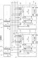
図1は、本発明の第1の実施形態における液晶表示装置の構成を示すブロック図である。当該液晶表示装置は、液晶表示パネル1と、データ線ドライバ21〜2nと、走査線ドライバ3と、LCDコントローラ4と、階調電源5とを備えている。データ線ドライバ21〜2nは、液晶表示パネル1のデータ線(図示されない)を駆動する。走査線ドライバ3は、液晶表示パネル1の走査線(図示されない)を駆動する。LCDコントローラ4は、データ線ドライバ21〜2nに、液晶表示パネル1の各画素の階調を示す画素データDINを供給する。加えて、LCDコントローラ4は、データ線ドライバ21〜2n及び走査線ドライバ3に制御信号(図示されない)を供給し、これによりデータ線ドライバ21〜2n及び走査線ドライバ3を制御する。(First embodiment)
FIG. 1 is a block diagram showing the configuration of the liquid crystal display device according to the first embodiment of the present invention. The liquid crystal display device includes a liquid
階調電源5は、階調電源電圧VE1〜VEmを発生する回路である。後述されるように、階調電源5によって生成された階調電源電圧VE1〜VEmは、リファレンス電圧V1〜Vmを生成するために使用される一組の電圧であり、下記の関係を満足する:
VE1>VE2>・・・>VEm.The
VE1 > VE2 >...> VEm .
図3に示されているように、階調電源5は、階調電源電圧VE1〜VEmをそれぞれに発生する電圧分割抵抗71〜7mを備えている。電圧分割抵抗71〜7mのそれぞれは、電源端子8と接地端子9との間に接続されており、その中間に設けられた中間ノード11から階調電源電圧VE1〜VEmを出力する。As shown in FIG. 3, the
電源ライン6は、階調電源電圧VE1〜VEmから生成されたリファレンス電圧V1〜Vmをデータ線ドライバ21〜2nのそれぞれに分配するために使用される;図3では、リファレンス電圧Viをデータ線ドライバ21〜2nに分配する電源ライン6が、符号「6i」によって示されている。The power line 6 is used to distribute the reference voltages V1 to Vm generated from the gradation power supply voltages VE1 to VEm to each of the
続いて、データ線ドライバ2の構成を詳細に説明する。データ線ドライバ21〜2nのそれぞれは、データレジスタ21と、ラッチ回路22と、γ抵抗ラダー回路23と、D/Aコンバータ24と、出力回路25とを備えている。データレジスタ21は、LCDコントローラ4から画素データDINを受け取って保存する。ラッチ回路22は、データレジスタ21から画素データDINをラッチし、ラッチした画素データDINをD/Aコンバータ24に転送する。γ抵抗ラダー回路23は、抵抗ラダーを用いた電圧分割により、下記関係を満足する階調電圧Vγ1〜Vγpをリファレンス電圧V1〜Vmから発生する:
Vγ1>Vγ2>・・・>Vγp.Next, the configuration of the
Vγ1 > Vγ2 >...> Vγp .
D/Aコンバータ24は、階調電圧Vγ1〜Vγpから、ラッチ回路22から受け取った画素データDINに対応する階調電圧を選択し、選択された階調電圧を出力回路25に出力する。出力回路25は、液晶表示パネル1のデータ線のそれぞれに接続されている電圧フォロア(図示されない)から構成されており、各データ線を、D/Aコンバータ24から供給された階調電圧に対応する駆動電圧に駆動する。D /
更に、γアンプ261〜26mが、データ線ドライバ21〜2nに分散して集積化されている。γアンプ261〜26mは、階調電源電圧VE1〜VEmからリファレンス電圧V1〜Vmを発生するために使用される演算増幅器である。γアンプ261〜26mは、基本的には、それぞれ階調電源電圧VE1〜VEmと一致するようにリファレンス電圧V1〜Vmを発生する。ただし、γアンプ261〜26mの動作により、リファレンス電圧V1〜Vmの微調整を行うことも可能である。本実施形態では、1つのデータ線ドライバ2に、2つのγアンプ26が集積化されている(従って、mは2nに等しい)。Further, γ amplifiers 261 to 26m are distributed and integrated in the
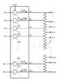
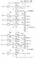
図4は、各データ線ドライバ2に集積化されたγ抵抗ラダー回路23の構成を示す図である。γ抵抗ラダー回路23は、最高階調電圧配線27と、抵抗ラダー28と、最低階調電圧配線29とを備えている。最高階調電圧配線27は、最高の階調電圧Vγ1をD/Aコンバータ24に供給する配線であり、外部入力パッド311に接続されている。外部入力パッド311は、電源ライン61を介してγアンプ261の出力に接続されており、従って、最高階調電圧配線27は、γアンプ261から供給された最高のリファレンス電圧V1を最高の階調電圧Vγ1としてそのままD/Aコンバータ24に供給する。FIG. 4 is a diagram showing a configuration of the γ
同様に、最低階調電圧配線29は、最低の階調電圧VγpをD/Aコンバータ24に供給する配線であり、外部入力パッド31mに接続されている。外部入力パッド31mは、電源ライン6mを介してγアンプ26mの出力に接続されており、従って、最低階調電圧配線29は、γアンプ26mから供給された最低のリファレンス電圧Vmを最低の階調電圧VγpとしてそのままD/Aコンバータ24に供給する。Similarly, the lowest
一方、抵抗ラダー28は、中間のリファレンス電圧V2〜Vm−2から中間の階調電圧Vγ2〜Vγp−1を電圧分割によって生成し、D/Aコンバータ24に供給する。抵抗ラダー28には、入力タップ302〜30m−1が設けられており、その入力タップ302〜30m−1は、それぞれ、外部入力パッド312〜31m−1に接続されている。外部入力パッド312〜31m−1は、それぞれ、電源ライン62〜6m−1を介してγアンプ262〜26m−2に接続されており、従って、入力タップ302〜30m−1には、それぞれリファレンス電圧V2〜Vm−1が供給される。リファレンス電圧V2〜Vm−2が供給されると、抵抗ラダー28の各出力タップから階調電圧Vγ2〜Vγp−2が出力される。On the other hand, the
本実施形態の液晶表示装置10の一つの特徴は、最も高い階調電圧Vγ1を供給する最高階調電圧配線27、及び最も低い階調電圧Vγpを供給する最低階調電圧配線29が抵抗ラダー28から切り離されている点にある。これにより、最高のリファレンス電圧V1を発生するγアンプ261の出力及び最も低い階調電圧Vγpを発生するγアンプ26mの出力が抵抗ラダー28から切り離され、リファレンス電圧V1、V2、Vm−1、Vmを生成するγアンプ261、262、26m−1、26mの出力に吸い込まれる電流、又は吐き出される電流が低減される。吸い込み電流/吐き出し電流の低減は、γアンプ261〜26mの内部のトランジスタに印加される電流/電圧バイアスを安定化し、γアンプ261〜26mのPSRR特性(power supply rejection ratio)を有効に向上させる。この結果、γアンプ261〜26mに供給される電源電圧が変動しても、リファレンス電圧が安定に保たれ、液晶表示パネルに表示される画像の画質の劣化が抑制される。One feature of the liquid crystal display device 10 of the present embodiment is that the highest
発明者は、最高階調電圧配線27及び最低階調電圧配線29を抵抗ラダー28から切り離すことによる吸い込み電流/吐き出し電流の低減及びリファレンス電圧の安定化の効果を、γアンプ26の数が18である場合(m=18)の場合についてシミュレーションによって検証した。より具体的には、γアンプ261、2618の出力が抵抗ラダー28に接続されている場合(図5A参照)と、γアンプ261、2618の出力が抵抗ラダー28に接続されていない場合(図5B参照)のそれぞれについて、γアンプ261、262、26m−1、26mの吸い込み電流/吐き出し電流の大きさ及びリファレンス電圧V1、V2の変動が、シミュレーションによって算出された。The inventor has the effect of reducing the sink current / discharge current and stabilizing the reference voltage by separating the highest
図5Aに示されているように、最高階調電圧配線27及び最低階調電圧配線29が抵抗ラダー28に接続されている場合、γアンプ261の出力から比較的大きな吐き出し電流(X1mA)が流れ出し、γアンプ262の出力に比較的大きな吸い込み電流(X2mA)が流れ込み、γアンプ26m−1の出力から比較的大きな吐き出し電流(X2mA)が流れ出し、γアンプ26mの出力に比較的大きな吸い込み電流(X1mA)が流れ込むという結果が得られた。更に、図6に示されているように、γアンプ261〜26mの電源電圧VDD2が周期的に変化した場合には、リファレンス電圧V1、V2も大きな変動を起こすという結果が得られた。As shown in Figure 5A, when the highest
更に、最高階調電圧配線27及び最低階調電圧配線29が抵抗ラダー28から切り離されている点以外は同一の条件でシミュレーションが行われた。その結果、γアンプ261、262、2617、2618の吸い込み電流/吐き出し電流が顕著に低減されるという結果が得られた。具体的には、図5Bに示されているように、γアンプ261、2618の吸い込み電流/吐き出し電流は0であり、γアンプ262の出力から比較的小さな吐き出し電流(Y(<X2)mA)が流れ出し、γアンプ2617の出力に比較的小さな吸い込み電流(YmA)が流れ込む、という結果が得られた。更に、図6に示されているように、γアンプ261〜26mの電源電圧VDD2が周期的に変化した場合でも、リファレンス電圧V1、V2の変動は小さいという結果が得られた。Further, the simulation was performed under the same conditions except that the highest
なお、本実施形態では、最高階調電圧配線27及び最低階調電圧配線29の両方が、抵抗ラダー28から電気的に切り離されている構成が提示されているが、一方のみが抵抗ラダー28から電気的に切り離されていてもよい。このような構成でも吸い込み電流/吐き出し電流の低減、及びリファレンス電圧V1、V2の変動の抑制という効果が得られることは当業者には自明的である。In the present embodiment, a configuration is shown in which both the highest
(第2の実施形態)
液晶表示装置の製造業者が要望するリファレンス電圧の組み合わせは、液晶表示装置の製造者によって異なることがある。より具体的には、或る製造業者は、m本のリファレンス電圧V1〜Vmをデータ線ドライバに供給することを望む一方、他の製造業者は、高いほうから2番目のリファレンス電圧V2及び低いほうから2番目のリファレンス電圧Vm−1の供給を省略したいと望む場合がある。(Second Embodiment)
The combination of reference voltages desired by the manufacturer of the liquid crystal display device may differ depending on the manufacturer of the liquid crystal display device. More specifically, some manufacturers desire to supplym reference voltages V1 -Vm to the data line driver, while other manufacturers have the second highest reference voltage V2. In some cases, it may be desirable to omit the supply of the second lowest reference voltage Vm−1 .
両方の製造業者の要求を同時に満足させる上の一つの問題は、図7に示されているように、第1の実施形態のγ抵抗ラダー回路23の構成では、リファレンス電圧V2、Vm−1の供給を省略すると所望の階調電圧が生成されないことである。リファレンス電圧V2の供給が停止されると、入力タップ302、303の間の出力タップには、所望の階調電圧が生成されない。同様に、リファレンス電圧Vm−1の供給が停止されると、入力タップ30m−1、30mの間の出力タップには、所望の階調電圧が生成されない。One problem in satisfying the requirements of both manufacturers at the same time is that, as shown in FIG. 7, in the configuration of the γ
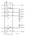
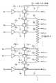
このような問題を解決するために、第2の実施形態では、各データ線ドライバ2に搭載されるγ抵抗ラダー回路の構成が修正される。図8、図9は、本発明の第2の実施形態におけるγ抵抗ラダー回路23Aの構成を示す回路図である。第2の実施形態では、各データ線ドライバ2iに、電源ライン61〜6mのそれぞれに対応する外部入力パッド311〜31mに加えてダミーパッド32、33が設けられる。ダミーパッド32は、抵抗素子34を介して抵抗ラダー28の入力タップ302に接続され、ダミーパッド33は、抵抗素子35を介して抵抗ラダー28の入力タップ30m−1に接続される。In order to solve such a problem, in the second embodiment, the configuration of the γ resistance ladder circuit mounted on each
このような構成のγ抵抗ラダー回路23Aは、リファレンス電圧V1〜Vmの全てをデータ線ドライバに供給することを望む製造業者と、リファレンス電圧V2、Vm−1の供給を望まない製造業者の両方の要求を、データ線ドライバ2の外部の配線に僅かな変更を加えることによって満足させることができる。図8に示されているように、リファレンス電圧V1〜Vmの全てが供給される場合には、リファレンス電圧V1〜Vmが、それぞれ、外部入力パッド311〜31mに供給される。The γ resistor ladder circuit 23A having such a configuration is manufactured by a manufacturer who wants to supply all of the reference voltages V1 to Vm to the data line driver, and a manufacturer who does not want to supply the reference voltages V2 and Vm−1. Both requirements of the merchant can be satisfied by making minor changes to the wiring external to the
一方、リファレンス電圧V2、Vm−1の供給が省略される場合、図9に示されているように、リファレンス電圧V1を生成するγアンプ261の出力が外部配線36によってダミーパッド32に接続され、リファレンス電圧Vmを生成するγアンプ26mの出力が外部配線37によってダミーパッド33に接続される。これにより、リファレンス電圧V1、Vmがダミーパッド32、33に供給される。抵抗素子34、35の抵抗値が適切に定められていれば、リファレンス電圧V2、Vm−1が供給されなくても、リファレンス電圧V1、Vmをダミーパッド32、33に供給することによって所望の階調電圧Vγ2〜Vγp−1を生成することが可能である。On the other hand, when the supply of the reference voltage V2, Vm-1 is omitted, as shown in Figure 9, the dummy pad 32 outputs the γ amplifier 261 to generate the reference voltage V1 is the
なお、上述の実施形態において、液晶表示パネル1が単一のデータ線ドライバ2によって駆動される場合には、その単一のデータ線ドライバ2に、全てのγアンプ261〜26mが集積化されてもよい。この場合、リファレンス電圧V1〜Vmを抵抗ラダー28に供給する電源ライン61〜6mも、その単一のデータ線ドライバ2に集積化される。In the above-described embodiment, when the liquid
また、上述の実施形態には液晶表示パネルを備えた液晶表示装置が提示されているが、本発明が、他の表示パネルを電圧駆動する表示装置にも適用可能なことは、当業者には自明的である。 Moreover, although the liquid crystal display device provided with the liquid crystal display panel is shown in the above-mentioned embodiment, it is understood by those skilled in the art that the present invention can be applied to a display device that drives other display panels with voltage. It is self-explanatory.
1:液晶表示パネル
2:データ線ドライバ
3:走査線ドライバ
4:LCDコントローラ
5:階調電源
6:電源ライン
7:電圧分割抵抗
8:電源端子
9:接地端子
11:中間ノード
21:データレジスタ
22:ラッチ回路
23、23A:γ抵抗ラダー回路
24:D/Aコンバータ
25:出力回路
26:γアンプ
27:最高階調電圧配線
28:抵抗ラダー
29:最低階調電圧配線
30:入力タップ
31:外部入力パッド
32、33:ダミーパッド
34、35:抵抗素子
36、37:外部配線
100:階調電圧発生回路
101:γアンプ
102:抵抗ラダー
103:入力タップ1: liquid crystal display panel 2: data line driver 3: scanning line driver 4: LCD controller 5: gradation power supply 6: power supply line 7: voltage dividing resistor 8: power supply terminal 9: ground terminal 11: intermediate node 21: data register 22 :
Claims (9)
Translated fromJapanese少なくとも一のデータ線ドライバと、
前記データ線ドライバのいずれかに集積化されている、複数のリファレンス電圧をそれぞれに生成する複数の演算増幅器
とを具備し、
前記データ線ドライバは、
前記表示パネルを駆動する駆動回路と、
前記複数のリファレンス電圧のうち最も高い最高リファレンス電圧を前記複数の演算増幅器のうちの第1演算増幅器から供給され、供給された前記最高リファレンス電圧を最高階調電圧として前記駆動回路に供給する最高階調電圧配線と、
前記最高リファレンス電圧以外の前記複数のリファレンス電圧を前記第1演算増幅器以外の前記複数の演算増幅器からそれぞれに受け取り、前記最高階調電圧よりも低い複数の階調電圧を生成する抵抗ラダー
とを備え、
前記駆動回路は、前記表示パネルのデータ線を、前記最高階調電圧、及び前記複数の階調電圧を用いて駆動し、
前記複数の演算増幅器は、前記複数のリファレンス電圧を前記データ線ドライバの外部にそれぞれに出力し、
前記データ線ドライバは、更に、
前記抵抗ラダーに設けられた複数の入力タップのそれぞれに接続された複数のパッドと、
第1ダミーパッドと、
前記複数の入力タップのうちの一端に位置する入力タップと前記第1ダミーパッドとの間に設けられた第1抵抗素子
とを備え、
前記最高階調電圧配線は、前記データ線ドライバの内部においては前記抵抗ラダーから切り離されている
表示装置。A display panel;
At least one data line driver;
A plurality of operational amplifiers, each of which generates a plurality of reference voltages, integrated in any of the data line drivers,
The data line driver is
A drive circuit for driving the display panel;
The highest highest reference voltage among the plurality of reference voltages is supplied from the first operational amplifier of the plurality of operational amplifiers, and the highest reference voltage is supplied to the drive circuit as the highest gradation voltage. Voltage regulator wiring,
A resistor ladder that receives the plurality of reference voltages other than the highest reference voltage from the plurality of operational amplifiers other than the first operational amplifier, and generates a plurality of gradation voltages lower than the highest gradation voltage. ,
The drive circuit drives the data line of the display panel using the highest gradation voltage and the plurality of gradation voltages,
The plurality of operational amplifiers output the plurality of reference voltages to the outside of the data line driver,
The data line driver further includes:
A plurality of pads connected to each of a plurality of input taps provided in the resistance ladder;
A first dummy pad;
A first resistance element provided between an input tap located at one end of the plurality of input taps and the first dummy pad
And
The highest gradation voltage wiring is separated from the resistance ladderinside the data line driver .
前記第1ダミーパッドが、前記データ線ドライバの外部の配線を介して前記第1演算増幅器の出力に接続されている
表示装置。The display device according to claim 1,
The display device,wherein the first dummy pad is connected to an output of the first operational amplifier via a wiring external to the data line driver .
前記データ線ドライバのいずれかに集積化されている、前記複数のリファレンス電圧のいずれよりも低い最低リファレンス電圧を生成する第2演算増幅器を更に具備し、
前記データ線ドライバは、前記最低リファレンス電圧を前記第2演算増幅器から供給され、供給された前記最低リファレンス電圧を最低階調電圧として前記駆動回路に供給する最低階調電圧配線を更に備え、
前記駆動回路は、前記表示パネルのデータ線を、前記最高階調電圧、前記複数の階調電圧、及び前記最低階調電圧を用いて駆動し、
前記データ線ドライバは、更に、
第2ダミーパッドと、
前記複数の入力タップのうちの他端に位置する入力タップと前記第2ダミーパッドとの間に設けられた第2抵抗素子
とを備え、
前記最低階調電圧配線は、前記データ線ドライバの内部においては前記抵抗ラダーから切り離されている
表示装置。The display device according to claim 1or 2 ,
A second operational amplifier that is integrated in any of the data line drivers and generates a lowest reference voltage lower than any of the plurality of reference voltages;
The data line driver further includes a lowest gradation voltage wiring that supplies the lowest reference voltage from the second operational amplifier and supplies the supplied lowest reference voltage as the lowest gradation voltage to the driving circuit,
The drive circuit drives the data line of the display panel using the highest gradation voltage, the plurality of gradation voltages, and the lowest gradation voltage,
The data line driver further includes:
A second dummy pad;
A second resistance element provided between the input tap located at the other end of the plurality of input taps and the second dummy pad
And
The lowest gradation voltage wiring is separated from the resistance ladderinside the data line driver .
前記第2ダミーパッドが、前記データ線ドライバの外部の配線を介して前記第2演算増幅器の出力に接続されている
表示装置。The display device according to claim 3,
The display device,wherein the second dummy pad is connected to an output of the second operational amplifier via a wiring external to the data line driver .
少なくとも一のデータ線ドライバと、
前記データ線ドライバのいずれかに集積化されている、複数のリファレンス電圧をそれぞれに生成する複数の演算増幅器
とを具備し、
前記データ線ドライバは、
前記表示パネルを駆動する駆動回路と、
前記複数のリファレンス電圧のうち最も低い最低リファレンス電圧を前記複数の演算増幅器のうちの第1演算増幅器から供給され、供給された前記最低リファレンス電圧を最低階調電圧として前記駆動回路に供給する最低階調電圧配線と、
前記最低リファレンス電圧以外の前記複数のリファレンス電圧を前記第1演算増幅器以外の前記複数の演算増幅器からそれぞれに受け取り、前記最低階調電圧よりも高い複数の階調電圧を生成する抵抗ラダー
とを備え、
前記駆動回路は、前記表示パネルのデータ線を、前記最低階調電圧、及び前記複数の階調電圧を用いて駆動し、
前記複数の演算増幅器は、前記複数のリファレンス電圧を前記データ線ドライバの外部にそれぞれに出力し、
前記データ線ドライバは、更に、
前記抵抗ラダーに設けられた複数の入力タップのそれぞれに接続された複数のパッドと、
ダミーパッドと、
前記複数の入力タップのうちの端に位置する入力タップと前記ダミーパッドとの間に設けられた抵抗素子
とを備え、
前記最低階調電圧配線は、前記データ線ドライバの内部においては前記抵抗ラダーから切り離されている
表示装置。A display panel;
At least one data line driver;
A plurality of operational amplifiers, each of which generates a plurality of reference voltages, integrated in any of the data line drivers,
The data line driver is
A drive circuit for driving the display panel;
The lowest lowest reference voltage of the plurality of reference voltages is supplied from the first operational amplifier of the plurality of operational amplifiers, and the supplied lowest reference voltage is supplied to the driving circuit as the lowest gradation voltage. Voltage regulator wiring,
Receiving each of the plurality of reference voltages other than the lowest reference voltage from said plurality of operational amplifiers other than the first operational amplifier, a resistor ladder, wherein generating ahigh has plurality of gradation voltages thanlowest gradation voltage With
Wherein the drive circuit, a data line of the display panel to drive by using theminimum gray-scale voltage and said plurality of gray scale voltages,
The plurality of operational amplifiers output the plurality of reference voltages to the outside of the data line driver,
The data line driver further includes:
A plurality of pads connected to each of a plurality of input taps provided in the resistance ladder;
Dummy pad,
Resistance element provided between the input tap located at the end of the plurality of input taps and the dummy pad
And
Thelowest gradation voltage lines, the display device that is disconnected from the resistorladder in the interior of the data line driver.
前記ダミーパッドが、前記データ線ドライバの外部の配線を介して前記第1演算増幅器の出力に接続されているThe dummy pad is connected to the output of the first operational amplifier via a wiring external to the data line driver.
表示装置。Display device.
前記複数のリファレンス電圧の少なくとも一を生成する演算増幅器と、
表示パネルを駆動する駆動回路と、
前記複数のリファレンス電圧のうち最も高い最高リファレンス電圧を供給され、供給された前記最高リファレンス電圧を最高階調電圧として前記駆動回路に供給する最高階調電圧配線と、
前記最高リファレンス電圧以外の前記複数のリファレンス電圧を受け取り、前記最高階調電圧よりも低い複数の階調電圧を生成する抵抗ラダーと、
前記抵抗ラダーに設けられた複数の入力タップのそれぞれに接続された複数のパッドと、
第1ダミーパッドと、
前記複数の入力タップのうちの一端に位置する入力タップと前記第1ダミーパッドとの間に設けられた第1抵抗素子
とを具備し、
前記駆動回路は、前記表示パネルのデータ線を、前記最高階調電圧、及び前記複数の階調電圧を用いて駆動し、
前記最高階調電圧配線は、前記抵抗ラダーから切り離されている
表示パネルドライバ。A display panel driver configured to generate a gradation voltage from a plurality of reference voltages,
An operational amplifier for generating at least one of the plurality of reference voltages;
A drive circuit for driving the display panel;
The highest gradation voltage wiring that is supplied with the highest highest reference voltage among the plurality of reference voltages and supplies the supplied highest reference voltage as the highest gradation voltage to the drive circuit;
A resistor ladder that receives the plurality of reference voltages other than the highest reference voltage and generates a plurality of gradation voltages lower than the highest gradation voltage;
A plurality of pads connected to each of a plurality of input taps provided in the resistance ladder;
A first dummy pad;
A first resistance element provided between the input tap located at one end of the plurality of input taps and the first dummy pad ;
The drive circuit drives the data line of the display panel using the highest gradation voltage and the plurality of gradation voltages,
The highest gradation voltage wiring is separated from the resistor ladder. Display panel driver.
前記複数のリファレンス電圧のいずれよりも低い最低リファレンス電圧を供給され、前記最低リファレンス電圧を最低階調電圧として前記駆動回路に供給する最低階調電圧配線と、
第2ダミーパッドと、
前記複数の入力タップのうちの他端に位置する入力タップと前記第2ダミーパッドとの間に設けられた第2抵抗素子
を更に具備し、
前記駆動回路は、前記表示パネルのデータ線を、前記最高階調電圧、前記複数の階調電圧、及び前記最低階調電圧を用いて駆動し、
前記最低階調電圧配線は、前記抵抗ラダーから切り離されている
表示パネルドライバ。The display panel driver according to claim7 ,
A lowest gradation voltage wiringthat is supplied with the lowest reference voltage lower than any of the plurality of reference voltages and supplies the lowest reference voltage as the lowest gradation voltage to the drive circuit;
A second dummy pad;
A second resistance element provided between the input tap located at the other end of the plurality of input taps and the second dummy pad ;
The drive circuit drives the data line of the display panel using the highest gradation voltage, the plurality of gradation voltages, and the lowest gradation voltage,
The display panel driver, wherein the lowest gradation voltage wiring is separated from the resistor ladder.
前記複数のリファレンス電圧の少なくとも一を生成する演算増幅器と、An operational amplifier for generating at least one of the plurality of reference voltages;
表示パネルを駆動する駆動回路と、A drive circuit for driving the display panel;
前記複数のリファレンス電圧のうち最も低い最低リファレンス電圧を前記複数の演算増幅器のうちの第1演算増幅器から供給され、供給された前記最低リファレンス電圧を最低階調電圧として前記駆動回路に供給する最低階調電圧配線と、The lowest lowest reference voltage of the plurality of reference voltages is supplied from the first operational amplifier of the plurality of operational amplifiers, and the supplied lowest reference voltage is supplied to the driving circuit as the lowest gradation voltage. Voltage regulator wiring,
前記最低リファレンス電圧以外の前記複数のリファレンス電圧を前記第1演算増幅器以外の前記複数の演算増幅器からそれぞれに受け取り、前記最低階調電圧よりも高い複数の階調電圧を生成する抵抗ラダーと、A resistor ladder that receives the plurality of reference voltages other than the lowest reference voltage from each of the plurality of operational amplifiers other than the first operational amplifier, and generates a plurality of gradation voltages higher than the lowest gradation voltage;
前記抵抗ラダーに設けられた複数の入力タップのそれぞれに接続された複数のパッドと、A plurality of pads connected to each of a plurality of input taps provided in the resistance ladder;
ダミーパッドと、Dummy pad,
前記複数の入力タップのうちの一端に位置する入力タップと前記ダミーパッドとの間に設けられた抵抗素子Resistance element provided between the input tap located at one end of the plurality of input taps and the dummy pad
とを具備し、And
前記駆動回路は、前記表示パネルのデータ線を、前記最低階調電圧、及び前記複数の階調電圧を用いて駆動し、The drive circuit drives the data line of the display panel using the lowest gradation voltage and the plurality of gradation voltages,
前記最低階調電圧配線は、前記抵抗ラダーから切り離されているThe lowest gradation voltage wiring is separated from the resistance ladder.
表示パネルドライバ。Display panel driver.
Priority Applications (5)
| Application Number | Priority Date | Filing Date | Title |
|---|---|---|---|
| JP2006289512AJP4936854B2 (en) | 2006-10-25 | 2006-10-25 | Display device and display panel driver |
| US11/905,812US20080100646A1 (en) | 2006-10-25 | 2007-10-04 | Display device and display panel driver using grayscale voltages which correspond to grayscales |
| TW096138849ATW200834529A (en) | 2006-10-25 | 2007-10-17 | Display device and display panel driver using grayscale voltages which correspond to grayscales |
| KR1020070107304AKR100903533B1 (en) | 2006-10-25 | 2007-10-24 | Display device and display panel driver using grayscale voltages which correspond to grayscales |
| CN2007101812139ACN101169915B (en) | 2006-10-25 | 2007-10-25 | Display device and display panel driver using grayscale voltages which correspond to grayscales |
Applications Claiming Priority (1)
| Application Number | Priority Date | Filing Date | Title |
|---|---|---|---|
| JP2006289512AJP4936854B2 (en) | 2006-10-25 | 2006-10-25 | Display device and display panel driver |
Publications (2)
| Publication Number | Publication Date |
|---|---|
| JP2008107516A JP2008107516A (en) | 2008-05-08 |
| JP4936854B2true JP4936854B2 (en) | 2012-05-23 |
Family
ID=39329577
Family Applications (1)
| Application Number | Title | Priority Date | Filing Date |
|---|---|---|---|
| JP2006289512AExpired - Fee RelatedJP4936854B2 (en) | 2006-10-25 | 2006-10-25 | Display device and display panel driver |
Country Status (5)
| Country | Link |
|---|---|
| US (1) | US20080100646A1 (en) |
| JP (1) | JP4936854B2 (en) |
| KR (1) | KR100903533B1 (en) |
| CN (1) | CN101169915B (en) |
| TW (1) | TW200834529A (en) |
Families Citing this family (14)
| Publication number | Priority date | Publication date | Assignee | Title |
|---|---|---|---|---|
| TWI390497B (en)* | 2008-06-20 | 2013-03-21 | Novatek Microelectronics Corp | Source driver and liquid crystal display |
| CN101640032B (en)* | 2008-07-29 | 2011-08-31 | 联咏科技股份有限公司 | Electronic device for improving voltage driving efficiency and related liquid crystal display |
| TWI413075B (en)* | 2009-04-06 | 2013-10-21 | Chunghwa Picture Tubes Ltd | Display and gamma correction circuit thereof |
| TW201239845A (en)* | 2011-02-14 | 2012-10-01 | Samsung Electronics Co Ltd | Systems and methods for driving a display device |
| KR20130035782A (en) | 2011-09-30 | 2013-04-09 | 엘지디스플레이 주식회사 | Method for driving organic light emitting display device |
| KR101931248B1 (en)* | 2012-12-27 | 2019-03-13 | 엘지디스플레이 주식회사 | Display device and method of manufacturing the same |
| JP2015090414A (en)* | 2013-11-06 | 2015-05-11 | シナプティクス・ディスプレイ・デバイス株式会社 | Display drive circuit and display device |
| EP3239086B1 (en)* | 2016-04-28 | 2022-06-01 | KONE Corporation | Solution for monitoring an elevator brake |
| US10200059B2 (en)* | 2016-09-22 | 2019-02-05 | Apple Inc. | Digital to analog converter |
| WO2018061917A1 (en)* | 2016-09-27 | 2018-04-05 | シャープ株式会社 | Display device |
| KR102441202B1 (en) | 2017-11-17 | 2022-09-06 | 주식회사 엘엑스세미콘 | Drive IC and display including it |
| CN109830210B (en) | 2019-01-25 | 2021-03-12 | 合肥鑫晟光电科技有限公司 | Set voltage generating unit, set voltage generating method and display device |
| US12067954B2 (en)* | 2019-06-27 | 2024-08-20 | Lapis Semiconductor Co., Ltd. | Display driver, semiconductor device, and amplifier circuit having a response-speed increase circuit |
| JP7286498B2 (en)* | 2019-09-24 | 2023-06-05 | ラピスセミコンダクタ株式会社 | Level voltage generation circuit, data driver and display device |
Family Cites Families (16)
| Publication number | Priority date | Publication date | Assignee | Title |
|---|---|---|---|---|
| JP2849010B2 (en)* | 1992-11-25 | 1999-01-20 | シャープ株式会社 | Display device drive circuit |
| US5854627A (en)* | 1994-11-11 | 1998-12-29 | Hitachi, Ltd. | TFT liquid crystal display device having a grayscale voltage generation circuit comprising the lowest power consumption resistive strings |
| JP4437378B2 (en)* | 2001-06-07 | 2010-03-24 | 株式会社日立製作所 | Liquid crystal drive device |
| JP2002366112A (en)* | 2001-06-07 | 2002-12-20 | Hitachi Ltd | Liquid crystal driving device and liquid crystal display device |
| JP2004157288A (en)* | 2002-11-06 | 2004-06-03 | Sharp Corp | Display device |
| JP4467877B2 (en)* | 2002-11-08 | 2010-05-26 | 富士通マイクロエレクトロニクス株式会社 | Display device driving method and display device driving circuit |
| JP2005010276A (en)* | 2003-06-17 | 2005-01-13 | Seiko Epson Corp | Gamma correction circuit, liquid crystal drive circuit, display device, power supply circuit |
| JP2005077507A (en)* | 2003-08-28 | 2005-03-24 | Optrex Corp | Gradation voltage generating circuit |
| KR100962503B1 (en)* | 2003-11-22 | 2010-06-15 | 엘지디스플레이 주식회사 | Gamma Correction Circuit of LCD |
| JP4199141B2 (en)* | 2004-02-23 | 2008-12-17 | 東芝松下ディスプレイテクノロジー株式会社 | Display signal processing device and display device |
| JP4193771B2 (en)* | 2004-07-27 | 2008-12-10 | セイコーエプソン株式会社 | Gradation voltage generation circuit and drive circuit |
| JP4643954B2 (en)* | 2004-09-09 | 2011-03-02 | ルネサスエレクトロニクス株式会社 | Gradation voltage generation circuit and gradation voltage generation method |
| JP4413730B2 (en)* | 2004-09-28 | 2010-02-10 | 富士通株式会社 | Liquid crystal display device and driving method thereof |
| JP4738867B2 (en)* | 2004-10-22 | 2011-08-03 | ルネサスエレクトロニクス株式会社 | Display device drive device |
| JP2006318381A (en)* | 2005-05-16 | 2006-11-24 | Seiko Epson Corp | Voltage generation circuit |
| KR100725976B1 (en)* | 2005-12-27 | 2007-06-08 | 삼성전자주식회사 | Gamma Adjustment Circuit and Gamma Adjustment Method |
- 2006
- 2006-10-25JPJP2006289512Apatent/JP4936854B2/ennot_activeExpired - Fee Related
- 2007
- 2007-10-04USUS11/905,812patent/US20080100646A1/ennot_activeAbandoned
- 2007-10-17TWTW096138849Apatent/TW200834529A/enunknown
- 2007-10-24KRKR1020070107304Apatent/KR100903533B1/ennot_activeExpired - Fee Related
- 2007-10-25CNCN2007101812139Apatent/CN101169915B/ennot_activeExpired - Fee Related
Also Published As
| Publication number | Publication date |
|---|---|
| JP2008107516A (en) | 2008-05-08 |
| KR100903533B1 (en) | 2009-06-23 |
| US20080100646A1 (en) | 2008-05-01 |
| TW200834529A (en) | 2008-08-16 |
| CN101169915A (en) | 2008-04-30 |
| KR20080037555A (en) | 2008-04-30 |
| CN101169915B (en) | 2011-02-16 |
Similar Documents
| Publication | Publication Date | Title |
|---|---|---|
| JP4936854B2 (en) | Display device and display panel driver | |
| JP4437378B2 (en) | Liquid crystal drive device | |
| JP5188023B2 (en) | Driving device and driving method thereof | |
| JP4102336B2 (en) | LCD drive circuit | |
| US8184078B2 (en) | Liquid crystal display and source driving circuit having a gamma and common voltage generator thereof | |
| CN101059947B (en) | Display and circuit for driving a display | |
| US20050012700A1 (en) | Gamma correction circuit, liquid crystal driving circuit, display and power supply circuit | |
| EP1763012A2 (en) | Light-emitting device and method of driving the same | |
| JP2006039205A (en) | Gradation voltage generation circuit, drive circuit, and electro-optical device | |
| US20110007057A1 (en) | Liquid crystal display driver and liquid crystal display device | |
| US20080122820A1 (en) | Gradation potential generation circuit, data driver of display device and the display device | |
| KR20090015344A (en) | Digital analog converter of digital display | |
| JP2009015166A (en) | Display device and display panel driver | |
| JP2013026647A (en) | Amplifier, liquid crystal display drive circuit, and liquid crystal display device | |
| US8310507B2 (en) | Display device drive circuit | |
| US6798146B2 (en) | Display apparatus and method of driving the same | |
| US7193403B2 (en) | Current driver | |
| JP2005345808A (en) | Source driving integrated circuit of lcd module and source driving system using the same | |
| JP4364742B2 (en) | Display drive device | |
| JP4859073B2 (en) | Liquid crystal drive device | |
| KR100508024B1 (en) | Analog voltage regulator for liquid crystal display | |
| JP2009157094A (en) | Data line driving circuit, driver ic, and display apparatus | |
| JP2006018148A (en) | Liquid crystal driving apparatus | |
| US20110001742A1 (en) | Voltage generating system | |
| KR100675318B1 (en) | Drive circuit of electro luminescence panel |
Legal Events
| Date | Code | Title | Description |
|---|---|---|---|
| A621 | Written request for application examination | Free format text:JAPANESE INTERMEDIATE CODE: A621 Effective date:20090716 | |
| A977 | Report on retrieval | Free format text:JAPANESE INTERMEDIATE CODE: A971007 Effective date:20111116 | |
| A131 | Notification of reasons for refusal | Free format text:JAPANESE INTERMEDIATE CODE: A131 Effective date:20111202 | |
| A521 | Request for written amendment filed | Free format text:JAPANESE INTERMEDIATE CODE: A523 Effective date:20120131 | |
| TRDD | Decision of grant or rejection written | ||
| A01 | Written decision to grant a patent or to grant a registration (utility model) | Free format text:JAPANESE INTERMEDIATE CODE: A01 Effective date:20120221 | |
| A01 | Written decision to grant a patent or to grant a registration (utility model) | Free format text:JAPANESE INTERMEDIATE CODE: A01 | |
| A61 | First payment of annual fees (during grant procedure) | Free format text:JAPANESE INTERMEDIATE CODE: A61 Effective date:20120221 | |
| FPAY | Renewal fee payment (event date is renewal date of database) | Free format text:PAYMENT UNTIL: 20150302 Year of fee payment:3 | |
| R150 | Certificate of patent or registration of utility model | Free format text:JAPANESE INTERMEDIATE CODE: R150 | |
| S531 | Written request for registration of change of domicile | Free format text:JAPANESE INTERMEDIATE CODE: R313531 | |
| R350 | Written notification of registration of transfer | Free format text:JAPANESE INTERMEDIATE CODE: R350 | |
| LAPS | Cancellation because of no payment of annual fees |