JP4934193B2 - Substrate processing chamber using dielectric barrier discharge lamp assembly - Google Patents
Substrate processing chamber using dielectric barrier discharge lamp assemblyDownload PDFInfo
- Publication number
- JP4934193B2 JP4934193B2JP2009507992AJP2009507992AJP4934193B2JP 4934193 B2JP4934193 B2JP 4934193B2JP 2009507992 AJP2009507992 AJP 2009507992AJP 2009507992 AJP2009507992 AJP 2009507992AJP 4934193 B2JP4934193 B2JP 4934193B2
- Authority
- JP
- Japan
- Prior art keywords
- gas
- discharge
- electrode
- lamp assembly
- dielectric barrier
- Prior art date
- Legal status (The legal status is an assumption and is not a legal conclusion. Google has not performed a legal analysis and makes no representation as to the accuracy of the status listed.)
- Expired - Fee Related
Links
Images


Classifications
- H—ELECTRICITY
- H01—ELECTRIC ELEMENTS
- H01L—SEMICONDUCTOR DEVICES NOT COVERED BY CLASS H10
- H01L21/00—Processes or apparatus adapted for the manufacture or treatment of semiconductor or solid state devices or of parts thereof
- H01L21/67—Apparatus specially adapted for handling semiconductor or electric solid state devices during manufacture or treatment thereof; Apparatus specially adapted for handling wafers during manufacture or treatment of semiconductor or electric solid state devices or components ; Apparatus not specifically provided for elsewhere
- H01L21/67005—Apparatus not specifically provided for elsewhere
- H01L21/67011—Apparatus for manufacture or treatment
- H01L21/67098—Apparatus for thermal treatment
- H01L21/67115—Apparatus for thermal treatment mainly by radiation
- H—ELECTRICITY
- H01—ELECTRIC ELEMENTS
- H01J—ELECTRIC DISCHARGE TUBES OR DISCHARGE LAMPS
- H01J65/00—Lamps without any electrode inside the vessel; Lamps with at least one main electrode outside the vessel
- H—ELECTRICITY
- H01—ELECTRIC ELEMENTS
- H01J—ELECTRIC DISCHARGE TUBES OR DISCHARGE LAMPS
- H01J65/00—Lamps without any electrode inside the vessel; Lamps with at least one main electrode outside the vessel
- H01J65/04—Lamps in which a gas filling is excited to luminesce by an external electromagnetic field or by external corpuscular radiation, e.g. for indicating plasma display panels
- H01J65/042—Lamps in which a gas filling is excited to luminesce by an external electromagnetic field or by external corpuscular radiation, e.g. for indicating plasma display panels by an external electromagnetic field
- H01J65/046—Lamps in which a gas filling is excited to luminesce by an external electromagnetic field or by external corpuscular radiation, e.g. for indicating plasma display panels by an external electromagnetic field the field being produced by using capacitive means around the vessel
Landscapes
- Physics & Mathematics (AREA)
- Engineering & Computer Science (AREA)
- Plasma & Fusion (AREA)
- Electromagnetism (AREA)
- General Physics & Mathematics (AREA)
- Condensed Matter Physics & Semiconductors (AREA)
- Toxicology (AREA)
- Manufacturing & Machinery (AREA)
- Computer Hardware Design (AREA)
- Microelectronics & Electronic Packaging (AREA)
- Power Engineering (AREA)
- Health & Medical Sciences (AREA)
- Physical Or Chemical Processes And Apparatus (AREA)
- Drying Of Semiconductors (AREA)
Description
Translated fromJapanese 発明の分野
[0001]本発明は、一般的に、半導体処理ツールに関し、より具体的には、誘電体バリア放電ランプアセンブリを有する熱処理ツールに関する。Field of Invention
[0001] The present invention relates generally to semiconductor processing tools, and more specifically to thermal processing tools having a dielectric barrier discharge lamp assembly.
関連技術の説明
[0002]RTP(急速加熱処理)は、半導体製造中に基板をアニーリングするプロセスである。このプロセス中には、制御された環境下で、基板を、900℃以上の温度まで急速に加熱するために、熱放射が利用される。この温度は、該プロセスに応じて、1秒未満から数分間の特定の時間、維持される。該基板は、次に、さらなる処理の前に冷却される。Explanation of related technology
[0002] RTP (rapid heat treatment) is a process of annealing a substrate during semiconductor manufacturing. During this process, thermal radiation is utilized to rapidly heat the substrate to a temperature of 900 ° C. or higher in a controlled environment. This temperature is maintained for a specific time from less than 1 second to several minutes, depending on the process. The substrate is then cooled before further processing.
[0003]従来、RTPチャンバは、典型的には、放射熱源またはランプと、チャンバ本体と、基板支持アセンブリとを含む。該基板支持アセンブリは、該チャンバ本体内に配置され、処理中に基板を支持する。該放射熱源は、典型的には、該熱源によって生成された放射エネルギが、該基板支持アセンブリ上に位置決めされた該基板に作用するように、該チャンバ本体の上面に載置され、または、該チャンバの内壁部に埋め込まれている。石英窓は、典型的には、放射熱源と、プロセスチャンバ内の典型的に該基板が配置されている内部プロセス領域とを分離するために、該チャンバの上面に配置されている。 [0003] Conventionally, RTP chambers typically include a radiant heat source or lamp, a chamber body, and a substrate support assembly. The substrate support assembly is disposed within the chamber body and supports the substrate during processing. The radiant heat source is typically mounted on the upper surface of the chamber body such that the radiant energy generated by the heat source acts on the substrate positioned on the substrate support assembly, or It is embedded in the inner wall of the chamber. A quartz window is typically placed on the top surface of the chamber to separate the radiant heat source from the internal process region in which the substrate is typically located.
[0004]該ランプによって生成された放射エネルギは、熱放射の波の形をしている。この放射は、広帯域であり、典型的には、約800nm〜約1500nmのピーク波長を有する。該石英窓を通って該基板表面への透過の間に、放射エネルギの一部は、失われてもよい。例えば、約4000nm超の波長は、透過しない。従って、該石英窓は、約400nm〜約4000nm、またはさらにそれ以上、および赤外線領域(IR)の、該石英窓を通過する放射エネルギの波長の変化を引き起こす。これらの波長の放射エネルギは、該基板表面での光化学反応を促進するのには不十分であり、また、反応して該基板上に多量の膜を形成する際に利用可能な生成反応種の数を不十分なものとする場合がある。 [0004] The radiant energy generated by the lamp is in the form of a wave of thermal radiation. This radiation is broadband and typically has a peak wavelength of about 800 nm to about 1500 nm. During transmission through the quartz window to the substrate surface, some of the radiant energy may be lost. For example, wavelengths above about 4000 nm are not transmitted. Accordingly, the quartz window causes a change in the wavelength of radiant energy passing through the quartz window, from about 400 nm to about 4000 nm, or even more, and in the infrared region (IR). The radiant energy of these wavelengths is insufficient to promote photochemical reactions at the substrate surface, and the generated reactive species available when reacting to form a large amount of film on the substrate. The number may be insufficient.
[0005]そのため、熱処理チャンバ用の改良されたランプアセンブリに対する要求がある。 [0005] Therefore, there is a need for an improved lamp assembly for a heat treatment chamber.
[0006]誘電体バリア放電(dielectric barrier discharge;DBD)ランプアセンブリおよび該アセンブリを利用する方法を提供する。一実施形態において、熱処理チャンバは、チャンバ本体と、誘電体バリア放電ランプアセンブリとを含む。該誘電体バリア放電ランプアセンブリは、第1の電極と、第2の電極と、誘電体バリアとをさらに備える。該誘電体バリア放電ランプアセンブリは、該第1の電極と第2の電極との間に位置決めされる。該誘電体バリアは、該誘電体バリアと第2の電極との間に放電空間を画定する。回路構成が、該第1および第2の電極に結合され、該誘電体バリア放電ランプアセンブリを作動させるようになっている。 [0006] A dielectric barrier discharge (DBD) lamp assembly and methods utilizing the assembly are provided. In one embodiment, the thermal processing chamber includes a chamber body and a dielectric barrier discharge lamp assembly. The dielectric barrier discharge lamp assembly further includes a first electrode, a second electrode, and a dielectric barrier. The dielectric barrier discharge lamp assembly is positioned between the first electrode and the second electrode. The dielectric barrier defines a discharge space between the dielectric barrier and the second electrode. A circuit arrangement is coupled to the first and second electrodes to operate the dielectric barrier discharge lamp assembly.
[0007]別の実施形態においては、該熱処理チャンバは、内部容積を画定するチャンバ本体と、該チャンバ本体の内部容積に配置された基板支持アセンブリとを含む。放射加熱アセンブリは、該チャンバ本体を貫通して形成されたウィンドウを通して、該基板支持体に放射を向けるように位置決めされている。該放射加熱アセンブリと基板支持体との間に位置決めされた誘電体バリア放電ランプアセンブリは、該チャンバ本体の内部容積に放射するようになっているアセンブリである。 [0007] In another embodiment, the thermal processing chamber includes a chamber body defining an internal volume and a substrate support assembly disposed in the internal volume of the chamber body. A radiant heating assembly is positioned to direct radiation toward the substrate support through a window formed through the chamber body. A dielectric barrier discharge lamp assembly positioned between the radiant heating assembly and the substrate support is an assembly adapted to radiate into the interior volume of the chamber body.
[0008]また別の実施形態においては、基板を処理する方法は、処理チャンバ内に配置された基板支持アセンブリ上に基板を位置決めすることと、該基板を、放射加熱アセンブリによって生成された放射エネルギに曝露させることと、該基板を、誘電体バリア放電ランプアセンブリによって生成された第2の放射エネルギに曝露させることとを含む。 [0008] In yet another embodiment, a method of processing a substrate includes positioning a substrate on a substrate support assembly disposed within a processing chamber and applying the substrate to radiant energy generated by a radiant heating assembly. Exposing the substrate to a second radiant energy generated by the dielectric barrier discharge lamp assembly.
[0009]上に列挙した本発明の特徴部を詳細に理解できるように、上記で簡単にまとめた本発明のより具体的な説明を、そのいくつかを添付図面に図示されている本発明の実施形態を参照して行う。しかし、該添付図面は、この発明の典型的な実施形態のみを図示しており、そのため、本発明の範囲を限定するものと考えるべきではなく、従って、本発明は、他の等しく有効な実施形態を許容可能なことに留意すべきである。 [0009] In order to provide a thorough understanding of the features of the invention listed above, a more specific description of the invention, briefly summarized above, may be found in the present invention, some of which are illustrated in the accompanying drawings. This is done with reference to the embodiment. However, the accompanying drawings illustrate only typical embodiments of the invention, and therefore should not be considered as limiting the scope of the invention, so the invention is not limited to other equally effective implementations. It should be noted that the form is acceptable.
[0016]理解を容易にするために、図面に共通している同一の要素を指し示すために、可能であれば、同一の参照数字を用いている。一実施形態の該要素および特徴部は、追加的な詳述なしに、他の実施形態に有利に組み込むことができることが意図されている。 [0016] To facilitate understanding, identical reference numerals have been used, where possible, to designate identical elements that are common to the drawings. It is contemplated that the elements and features of one embodiment may be advantageously incorporated into other embodiments without additional details.
[0017]しかし、添付図面は、本発明の例示的な実施形態のみを図示しており、そのため、本発明の範囲を限定するものと考えるべきではなく、従って、本発明は、他の同様に有効な実施形態を許容可能なことに留意すべきである。 [0017] However, the accompanying drawings only illustrate exemplary embodiments of the invention and therefore should not be considered as limiting the scope of the invention, and therefore the invention is not limited to any other It should be noted that valid embodiments are acceptable.
[0018]本発明の実施形態は、IRとUVが組み合わされたエネルギを熱処理システム内で生成する装置および方法を提供する。こが組み合わされたエネルギは、基板表面での光化学反応を促進するのに利用され、それにより、該基板上での均一な熱処理を可能にする。該組み合わさった放射エネルギは、熱処理システム内で、誘電体バリア放電(DBD)ランプアセンブリを利用して得られ、それにより、有効かつ均一な基板処理を有利に容易にする。 [0018] Embodiments of the invention provide an apparatus and method for generating combined IR and UV energy in a thermal processing system. This combined energy is utilized to promote a photochemical reaction at the substrate surface, thereby enabling a uniform heat treatment on the substrate. The combined radiant energy is obtained in a thermal processing system utilizing a dielectric barrier discharge (DBD) lamp assembly, thereby advantageously facilitating effective and uniform substrate processing.
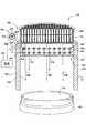
[0019]図1は、DBDランプアセンブリ150を有する急速熱処理チャンバ100の一実施形態の簡素化した断面斜視図である。本発明の利益を享受するように適応させることのできる急速熱処理チャンバの実例は、XEplusおよびRadiancePlus(商標)CENTURA(登録商標)熱処理システムであり、これらは共に、カリフォルニア州サンタクララにあるApplied Material,Inc.から入手可能である。誘電体バリア放電ランプアセンブリ150は、図示されている急速熱処理チャンバ100内で利用されるものとして記載されているが、誘電体バリア放電ランプアセンブリ150は、堆積チャンバ、エッチングチャンバおよび露光チャンバ等の他の熱処理システムでも利用することができる。 FIG. 1 is a simplified cross-sectional perspective view of one embodiment of a rapid
[0020]処理チャンバ100は、チャンバ壁部104と、底部110と、内部容積120を画定する上部112とを有するチャンバ本体102を含む。壁部104は、典型的には、基板140の出し入れを容易にするための少なくとも1つの基板アクセスポート148を含む。石英窓114は、チャンバ本体102の上部112に載置されている放射加熱アセンブリ106内に含まれている。放射加熱アセンブリ106は、基板支持体108内に位置決めされた基板140を加熱するのに利用される。放射加熱アセンブリ106は、ウォータージャケットアセンブリ162内に、複数のランプチューブ160を含む。各チューブ160は、リフレクタおよびタングステンハロゲンランプアセンブルを収容できる。ランプチューブ160は、ハニカムライトパイプ構成内に置かれている。ライトパイプのこの集密化された六角形構成は、高出力密度の約400nm〜約4000nmの波長を有するIR放射および/またはより長波長のUV放射等の放射エネルギを生成する。一実施形態において、放射加熱アセンブリ106は、該基板を熱処理するための、例えば、基板140上に配置されたシリコン層をアニーリングするための放射エネルギを生成する。本発明の利益を享受するように適応させることのできる1つの放射加熱アセンブリ106は、Gronet等に対して発行された米国特許第5,487,127号明細書に記載されており、その全体は参照により本明細書に組み込まれている。 [0020] The
[0021]誘電体バリア放電(DBD)ランプアセンブリ150は、放射加熱アセンブリ106と基板支持体108との間に配置されている。DBDランプ150は、放射加熱アセンブリ106の内面である接地電極と、該チャンバ本体と絶縁されている(図には示されていない絶縁)高電圧電極202と、誘電体バリア114とを備える。一実施形態において、該誘電体バリアは、放射加熱アセンブリ220のための石英窓である。DBDランプアセンブリ150は、基板処理を促進するのに利用される短波長の放射エネルギを生成する。放電空間152は、その中に放電ガスが供給されるDBDランプアセンブリ150内に画定されている。電源156は、放電空間152内に存在する放電ガスを活性化させる。活性化された放電ガスは、紫外線(UV)を放出し、それにより、該基板に、加熱アセンブリ106単独で生成されるものよりも高い流束のUV放射を照射する。一実施形態において、DBDランプアセンブリ150によって生成された放射エネルギは、約100nm〜約4000nmの波長を有するUVとIRが組み合わされた放射を含む。別の実施形態においては、DBDランプアセンブリ150によって生成された放射エネルギは、波長が約100nm〜1500nmのUV放射および/またはIR放射を有する。 [0021] A dielectric barrier discharge (DBD)
[0022]基板支持アセンブリ108は、その上に位置決めされる基板140を収容するために、チャンバ102の底部110上に配置されている。基板支持アセンブリ108は、基板140を回転させるように構成することができ、それにより、基板140を、放射加熱アセンブリ106およびDBDランプアセンブリ150によって生成された放射エネルギによって、コンフォーマルに加熱できるようにする。 [0022] The
[0023]回路構成154は、電源156によって、誘電体バリア放電ランプアセンブリ150に結合している。回路構成154は、電力をDBDランプアセンブリ150に与えるようになっている。作動時には、DBDランプアセンブリ150に印加される電圧が、電界を確立して、DBDランプアセンブリ150による放射エネルギの生成を可能にし、これにより、基板140の表面での反応および光化学プロセスが促進され、それによって、基板140上での熱処理を可能にする。また、放射加熱アセンブリ160は、熱エネルギを生成するランプ106に電力を供給するための独立した回路構成(図示せず)を有してもよい。放射加熱アセンブリ106から生成された熱エネルギは、基板140の表面に放射されて、十分な熱エネルギを与える。放射加熱アセンブリ106から生成された熱エネルギはまた、基板140の表面に放射されて基板140の表面を活性化させる、DBDランプアセンブリ150から生成された放射エネルギを増大させることもでき、それにより、基板140の表面での反応を促進する。 [0023] The
[0024]雰囲気制御システム164は、チャンバ本体102の内部容積120に結合されている。雰囲気制御システム164は、チャンバ圧力を制御するための絞り弁および真空ポンプを含む。また、雰囲気制御システム164は、追加的にプロセスガスまたは他のガスを内部容積120へ供給するガス源を含んでもよい。一実施形態において、雰囲気制御システム164は、熱堆積プロセスのためのプロセスガスを供給する。別の実施形態においては、雰囲気制御システム164は、アニーリングプロセスのためのガスを供給する。領域152内の放電ガスは、該雰囲気制御システムまたは独立した入口(図示せず)によって供給することができる。 [0024] The
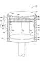
[0025]図2は、熱処理チャンバ200内に配置されたDBDランプアセンブリ150の一実施形態である。DBDランプアセンブリ150は、第1の電極220と、誘電体バリア114と、第2の電極202とを含む。第1の電極220は接地されている。第2の電極202は、チャンバ本体と絶縁されている(図には示されていない絶縁)。誘電体バリア114は、第1の電極220と第2の電極202との間に配置されており、第1の電極220と第2の電極202を離間関係に保つ。DBDランプアセンブリ150は、放射エネルギを生成して、基板140の表面を活性化するように構成されている。一実施形態において、第1の電極220は、図1に記載されている放射加熱アセンブリ106である。別の実施形態においては、第1の電極220は、放射エネルギを該基板に供給するのに適した他の構造を有してもよい。 [0025] FIG. 2 is one embodiment of a
[0026]第2の電極202は、電気を送り込んで、生成された放射エネルギを該第2の電極を通ることができるように構成された導電性材料である。一実施形態において、第2の電極202は、ワイヤグリッド、メタルメッシュ、有孔金属、エキスパンドメタルまたは導電性ウェブメタルである。第2の電極202の適切な材料は、限定されるものではないが、アルミニウム、ステンレス鋼、タングステン、銅、モリブデン、ニッケルおよび他の金属材料を含む。別の実施形態においては、第2の電極202は、上述したような導電性材料であって、誘電体層で被覆されているものであってもよい。また別の実施形態においては、第2の電極202は、隙間のあるパターンで誘電体層上に被覆された導電性材料であってもよい。該誘電体層は、放射エネルギの透過を容易にする透明な誘電体層または十分に薄い誘電体層とすることができる。該誘電体層の適切な材料は、限定されるものではないが、特に、MgO、SiO2、Y2O3、La2O3、CeO2、SrO、CaO、MgF2、LiF2およびCaF2を含む。該導電性材料は、インジウムスズ酸化物(indium tin oxide;ITO)、SnO2、W、Mo、Cuまたは別の金属とすることができる。[0026] The
[0027]誘電体バリア114は、プロセスを活性化する間、電流リミッタとして機能し、放射エネルギが、持続性のアーク放電に変わることを防ぐ。一実施形態において、誘電体バリア114は、放射エネルギを該誘電体バリアを通して放出できるようにする透明な誘電体材料である。別の実施形態においては、誘電体バリア114は、ガラス、石英、セラミックまたは他の適切なポリマー等の透明な誘電体材料である。また別の実施形態においては、該誘電体材料は、図1に記載されているような石英窓114である。 [0027] The
[0028]放電空間212は、処理チャンバ200内の誘電体バリア114と第2の電極202との間に画定されている。放電ガスは、放電空間212内に供給される。放電空間212は、放電容積に、放電空間212内で実行される、電子と該放電ガスとの間の十分な衝突を可能にさせる選択された放電距離210を有する。該放電容積は、エキシマーを含む励起された種を発生させることができ、それによって所望によりにUV放射を生成するように、電子と放電ガスの衝突を十分に促進するように構成される。一実施形態において、放電距離210は、放電空間212内での該衝突を促進するように適切な範囲内で選択される。別の実施形態においては、放電距離210は、約0.1cm〜約100cm、例えば、約2cm〜約20cmに選択される。加えて、放電空間212内の圧力は、約0.5トール〜約600トールに保つことができる。 [0028] A
[0029]電子と放電ガスの衝突は、エネルギを該放電ガスに与えて、放電プラズマ種およびエキシマーを含む反応種を発生させる。一部の活性化された反応種は、放射エネルギ、例えば、光子を放出して、基板140の表面へ放出するUV放射を引き起こす。基板140の表面は、該光子を吸収して、基板140の表面をエネルギ活性化状態にする。基板140のエネルギ活性化された表面は、該基板の反応、例えば、アニーリングプロセスまたは表面再構成を促進する。一実施形態において、放電ガスは、酸素ガス(O2)とすることができる。別の実施形態においては、該放電ガスは、酸素ガス(O2)、およびキセノンガス(Xe)、クリプトンガス(Kr)、アルゴンガス(Ar)、ネオンガス(Ne)、ヘリウムガス(He)等の希ガスを含む群より選択されたガス混合物であってもよい。また別の実施形態においては、該放電ガスは、酸素ガス(O2)、希ガス、ハロゲン含有ガス、フッ素、臭素、塩素ガス、ヨウ素含有ガス、H2OおよびNH3のうちの少なくとも1つを含むガス混合物であってもよい。[0029] The collision of the electrons with the discharge gas imparts energy to the discharge gas and generates reactive species including discharge plasma species and excimers. Some activated reactive species emit radiant energy, eg, photons, causing UV radiation to be emitted to the surface of the
[0030]要求に応じて、プロセス条件を最適化するために、プロセスガスを、プロセスチャンバ200の内部容積120に供給することができる。内部容積120に供給されたプロセスガスは、DBDランプアセンブリ150からのUV放射によって励起され、基板140の表面に対して、励起されたガス種を与える。該励起されたガス種ならびに該放電ガスによってエネルギ活性化された反応種は、該基板の表面をエネルギ活性化し、それにより、基板140上での光化学反応を誘発し、基板140が集中的かつ均一に処理されることを可能にする。図2に描かれている実施形態のように、第2の電極202は、金属メッシュまたはワイヤグリッド材料であるように構成されているため、該放電ガスは、第2の電極202を通って、基板表面140の全域にプロセスガスとして流れることができる。別の実施形態においては、該プロセスガスは、基板140の表面に個々に供給される該放電ガスとは異なっていてもよい。該プロセスガスは、酸素ガス(O2)、希ガス、ハロゲン含有ガス、H2O、N2O、N2またはNH3のうちの少なくとも1つを含むことができる。[0030] Process gas may be supplied to the
[0031]回路構成220は、電源250からの作動電圧を、第1の電極220および第2の電極202へ印加する。動作中、2つの電極220、202に印加された電圧は、放電空間212内での電子の衝突を促進する電界を確立する。この電子衝突は、放電空間212内で、該放電ガスへのエネルギを生成し、それにより、該放電ガスを、典型的には、反応種、放電種またはエキシマーと呼ばれる励起状態に活性化させる。該反応種は、後に再結合して、放射のかたちでエネルギ、例えばUV光子を放出する。放射エネルギ208は、基板140へ移動して、光化学的なプロセスおよび反応を促進する。UV放射208は、高い光子エネルギを生じ、それにより、基板140の表面に生じる光化学反応を促進し、該基板を均一に処理できるようにする。加えて、放射加熱アセンブリ106も、放射エネルギ208と同様に基板104の表面へ拡散する熱放射エネルギ206を生成して、それにより、組み合わされたIRおよびUV放射を生じさせて該基板反応を促進する。一実施形態において、DBDランプアセンブリ150によって生成されたUV放射208は、約100nm〜約400nmの波長を有する。別の実施形態においては、DBDランプアセンブリ150および放射加熱アセンブリ106によって生成された、組み合わされた熱放射エネルギ206およびUV放射208は、約100nm〜約4000nmの波長の組み合わされたIRおよびUV放射を有する。 [0031] The
[0032]電源250から回路構成204によって印加された電圧は、上述したようなエネルギを生成するのに十分である電界を確立することができるように選択される。一実施形態において、該電圧は、約100V〜約20,000V、例えば、約1,000V〜約5,000Vの範囲で印加することができる。 [0032] The voltage applied by the
[0033]図3は、熱処理チャンバ内のDBDランプアセンブリ150の一実施形態を描いた図である。DBDランプアセンブリ150は、第1の電極320と、第2の電極302と、誘電体バリア114とを含む。第1の電極320は、接地されている。第2の電極302は、該チャンバ本体と絶縁されている(図3には示されていない絶縁)。誘電体バリア114は、第1の電極320と第2の電極302との間に配置されており、第1の電極320と第2の電極302を離間関係に保つ。透明窓304は、DBDランプアセンブリ150の下に配置されている。図3に描かれている実施形態は、透明窓304を、任意選択的に、DBDランプアセンブリ150の下に配置することができることを除いて、図2に記載されている実施形態と実質的に同じであることに留意されたい。 [0033] FIG. 3 depicts one embodiment of a
[0034]プロセスチャンバ300内に配置された透明窓304は、DBDランプアセンブリ150と内部容積318とを分離する。分離されたDBDランプアセンブリ150は、放電空間314内の放電ガスを、DBDランプアセンブリ150内に収容できるようにし、それによって、該放電ガスの使用量を最小限にする。また、透明窓304は、DBDランプアセンブリ150と、処理チャンバ300の内部容積318とを分離し、それにより、無用のプラズマ種および他の放電種がDBDランプアセンブリ150から出るのを防ぐ。DBDランプアセンブリ150に関連する望ましくないスパッタされた物質、例えば、誘電体材料の衝撃に由来する粒子または汚染物質が、処理チャンバ300の内部容積318に入るのを有利に防ぐことができる。加えて、分離された放電空間314は、内部容積318に供給されたプロセスガスが、放電空間314内の放電ガスと混合するのを防ぎ、それにより、様々なプロセス要件に対する該プロセスガスおよび放電ガスの選択を最適化する。一実施形態において、該プロセスガスは、該放電ガスと同じでもよい。別の実施形態においては、内部容積318に供給される該プロセスガスは、酸素ガス(O2)、希ガス、ハロゲン含有ガス、H2O、N2O、N2およびNH3を含む群より選択される。[0034] A
[0035]透明窓304は、DBDランプアセンブリ150および放射加熱アセンブリ106内で生成された放射エネルギが、著しくエネルギを損失することなくことなく、該窓を通過できるように選択された材料で作られる。一実施形態において、透明窓304は、石英、ガラス基板、MgF2、CaF2またはLiF2のうちの少なくとも1つで作られる。[0035] The
[0036]図4は、熱処理チャンバ400内の内部分離された誘電体バリア放電ランプアセンブリ150の別の実施形態を描いた図である。図1に記載されているようなハニカムチューブ160および石英窓114を含む放射加熱アセンブリ106は、プロセスチャンバ400の上部面に配置されている。放射加熱アセンブリ106および誘電体バリア放電ランプアセンブリ150は、基板表面140に放射エネルギを与える。一実施形態において、放射加熱アセンブリ106から生成された放射エネルギは、IRおよび/またはより長波長のUV放射を有する。別の実施形態においては、放射加熱アセンブリ106から生成された放射エネルギは、約400nm〜約4000nmの波長を有する。 [0036] FIG. 4 depicts another embodiment of an internally separated dielectric barrier
[0037]第1の電極402、第2の電極408および誘電体バリア404および406を含む誘電体バリア放電ランプアセンブリ150は、放射加熱アセンブリ106の下に配置されている。DBDランプ150は、セグメント(図示せず)により、処理チャンバ400の壁部104から分離されていてもよく、または、該電極の一方を接地してもよい。一実施形態において、電極402、408は、電気を送り込み、および電圧の印加時に、放射エネルギを生成できるように構成された導電性材料である。別の実施形態においては、電極402、408は、ワイヤグリッド、メタルメッシュ、有孔金属、エキスパンドメタルまたは導電性ウェブ材料である。電極402、408の適切な材料は、限定されるものではないが、アルミニウム、ステンレス鋼、タングステン、銅、モリブデン、ニッケルおよび他の金属合金を含む。別の実施形態においては、電極402、408は、上述したような導電性材料であって、誘電体層で被覆されているものであってもよい。また別の実施形態においては、電極402、408は、符号404または406のような誘電体層上に被覆された導電性材料であってもよい。該誘電体層は、放射エネルギの透過を容易にする十分に薄い厚さを有する透明層または誘電体層とすることができる。該誘電体層の適切な材料は、限定されるものではないが、特に、MgO、SiO2、Y2O3、La2O3、CeO2、SrO、CaO、MgF2、LiF2およびCaF2を含む。該導電性材料は、前述したインジウムスズ酸化物(ITO)またはSnO2とすることができる。[0037] A dielectric barrier
[0038]誘電体層404および406は、第1の電極402と第2の電極408との間に配置されている。誘電体バリア404、406は、エネルギ活性化プロセスとの間、電流リミッタとして機能し、放射エネルギが、持続性のアーク放電に変わることを防ぐ。一実施形態において、誘電体バリア404、406は、放射エネルギを該誘電体バリアを通して放出できるようにする透明な誘電体材料である。別の実施形態においては、誘電体バリア404、406は、ガラス、石英、MgF2、CaF2およびLiF2、セラミックまたは他の適切なポリマー等の透明な誘電体材料である。[0038] The
[0039]また、誘電体バリア406は、透明窓としても役に立つことができる。透明窓406は、著しくエネルギを損失することなくことなく、DBDランプアセンブリ150および放射加熱アセンブリ106によって生成された放射エネルギの基板表面140への転送を容易にする材料で作られている。一実施形態において、該透明窓は、特に、石英、ガラス基板、MgF2、CaF2またはLiF2から作られる。別法として、2つの電極402、408が透明な誘電体層で被覆されている実施形態においては、透明窓406および誘電体層404は、省いて、任意選択的に、被覆された透明な誘電体層と置き換えてもよい。[0039] The
[0040]放電空間418は、処理チャンバ400内の誘電体バリア404と透明窓406との間に画定されている。放電ガスは、放電空間418に供給される。放電空間418は、放電空間418内での電子と放電ガスとの十分な衝突を可能にする放電容積を生じる選択された放電距離410を有する。この放電容積は、エキシマーを含む励起された種が生じて、それにより、所望によりにUV放射が生成されるように、該電子と放電ガスとの衝突を十分に促進するように構成されている。一実施形態において、放電距離410は、放電空間418内でのこの衝突を促進するように、適切な範囲内で選択される。別の実施形態においては、放電距離410は、約0.1cm〜約100cm、例えば、約2cm〜約20cmに選択される。また、放電空間418内の圧力は、約0.5トール〜約600トールに保つことができる。 [0040] A
[0041]放電空間418内での電子の衝突は、該放電ガスにエネルギを与えて、放電プラズマ種およびエキシマーを含む反応種を生じさせる。該反応種は、放射エネルギ、例えば、光子を放出して、基板140の表面へ放出するUV放射を生じさせる。透明窓406がDBDランプアセンブリ150内に配置されているため、該放電ガスは、該DBDランプアセンブリから出ることが防止され、それにより、プロセスガスを、処理チャンバ400の内部容積420に個々に供給することを可能にする。DBDランプアセンブリ150から生成されたUV放射は、内部容積420内の該プロセスガスを活性化して、該反応種を生じさせる。基板140の表面は、該プロセスガスから生成された反応種を吸収し、それにより、該基板の光化学的なプロセスおよび反応、例えば、酸化または窒化プロセスを促進する。また、放射加熱アセンブリ106から生成された放射エネルギは、該基板表面に放射され、それにより、組み合わされたIRおよびUV放射を生成して、該基板の表面を活性化し、基板140上での均一かつ強力なプロセス反応を可能にする。一実施形態において、該放電ガスおよびプロセスガスは、酸素ガス(O2)とすることができる。別の実施形態においては、該放電ガスおよびプロセスガスは、酸素ガス(O2)、およびキセノンガス(Xe)、クリプトンガス(Kr)、アルゴンガス(Ar)、ネオンガス(Ne)、ヘリウムガス(He)等の希ガスを含む群より選択されたガス混合物であってもよい。また別の実施形態においては、該放電ガスおよびプロセスガスは、酸素ガス(O2)、希ガス、ハロゲン含有ガス、フッ素、臭素、塩素ガス、ヨウ素含有ガス、H2O、N2O、N2およびNH3のうちの少なくとも1つを含むガス混合物であってもよい。さらに別の実施形態においては、該プロセスガスは、任意選択的に、該放電ガスと異なっていてもよい。[0041] The collision of electrons in the
[0042]回路構成412は、電源450からの作動電圧を、第1の電極402および第2の電極408に印加する。動作中、2つの電極402、408に印加された電圧は、放電空間418内での電子の衝突を促進する電界を確立する。この電子衝突は、放電空間418内で、該放電ガスへのエネルギを生成し、それにより、該放電ガスを、典型的には、反応種、放電種またはエキシマーと呼ばれる励起状態に活性化させる。これらの種の一部は、後に、放射416のかたちでエネルギ、例えば光子および/またはUV放射をDBDランプアセンブリ150から放出することによって、基底状態になる。放射エネルギ416は、基板140の表面に移動して、光化学的なプロセスおよび反応を促進する。UV放射416は、高い光子エネルギを生じ、それにより、基板140の表面に生じる光化学反応を促進し、該基板を均一に処理できるようにする。加えて、放射加熱アセンブリ106も、放射エネルギ416と同様に基板140の表面へ放射する熱放射エネルギ410を生成して、それにより、組み合わされたIRおよびUV放射を生じさせて該基板反応を促進する。一実施形態において、DBDランプアセンブリ150によって生成されたUV放射416は、約100nm〜約400nmの波長を有する。別の実施形態においては、DBDランプアセンブリ150および放射加熱アセンブリ106によって生成された、組み合わされた熱放射エネルギ414およびUV放射416は、約100nm〜約4000nmの波長の組み合わされたIRおよびUV放射を有する。 [0042] The
[0043]電源450を介して回路構成412によって印加された電圧は、十分な電界を確立してエネルギを生成できるように選択されてもよい。一実施形態において、該電圧は、約100V〜約20,000V、例えば、約1,000V〜約5,000Vの範囲で印加することができる。 [0043] The voltage applied by
[0044]プロセスチャンバ400内に配置された透明窓406は、内部分離された放電空間418と内部容積420とを分離する。分離された放電空間418は、該放電ガスを、DBDランプアセンブリ150内に収容できるようにし、それによって、該放電ガスの使用量を最小限にする。また、透明窓406は、放電ガスと、処理チャンバ400の内部容積420とを分離し、それにより、無用のプラズマ種および他の放電種が、DBDランプアセンブリ150から出るのを防ぐ。DBDランプアセンブリ150に関連する望ましくないスパッタされた物質、例えば、誘電体材料の衝撃に由来する粒子または汚染物質が、処理チャンバ400の内部容積420に入るのを有利に防ぐことができる。加えて、分離された放電空間418は、内部容積420に供給されたプロセスガスが、該放電ガスと混合するのを防ぎ、それにより、様々なプロセス要件に対する該プロセスガスおよび放電ガスの選択を最適化する。一実施形態において、該プロセスガスは、該放電ガスと同じでもよい。別の実施形態においては、内部容積318に供給される該プロセスガスは、酸素ガス(O2)、希ガス、ハロゲン含有ガス、H2O、N2O、N2およびNH3を含む群より選択される。[0044] A
[0045]図5は、熱処理チャンバ500内の内部分離されたDBDランプアセンブリ150の別の実施形態を描いた図である。図1に記載されているようなハニカムチューブ160および石英窓114を含む放射加熱アセンブリ106は、プロセスチャンバ500の上部面に配置されている。放射加熱アセンブリ106は、DBDランプアセンブリ150を介して基板表面140に放射エネルギ508を与える。一実施形態において、放射加熱アセンブリ106から生成された放射エネルギ508は、IRおよび/またはより長波長のUV放射を有する。別の実施形態においては、ランプアセンブリ106から生成された放射エネルギ508は、約400nm〜約4000nmの波長の放射を有する。 [0045] FIG. 5 depicts another embodiment of an internally separated
[0046]DBDランプアセンブリ150は、第1の電極502および第2の電極504を含む。電極502、504は、シリンダ522の中心に中空流路524を有する導電性シリンダ522上に被覆された誘電体層520を含み、それにより、冷却流体が該流路から流れることができるようになっている。一実施形態において、電極502、504は、互いに平行に位置決めされた2行のアレイを構成する。別の実施形態においては、電極502、504は、互いに平行に位置決めされた2枚の導電性シートであってもよい。また別の一実施形態において、電極502、504は、電気を送り込み、および電圧の印加時に、放射エネルギを生成できるように構成された導電性材料である。該電極の適切な材料は、限定されるものではないが、アルミニウム、ステンレス鋼、ニッケルおよび他の金属合金を含む。 [0046] The
[0047]シリンダ522上に被覆された誘電体層520は、誘電体材料である。該誘電体層は、放射エネルギの放出を容易にする十分に薄い厚さを有する透明層または誘電体層とすることができる。一実施形態において、該誘電体材料は、特に、MgO、SiO2、Y2O3、La2O3、CeO2、SrO、CaO、MgF2、LiF2およびCaF2を含む群より選択される。これらの電極間には、大きな空間があるため、該誘電体に対する透明性の要件は、緩和される場合がある。[0047] The
[0048]必要に応じて、シリンダ522の温度を調節するために、冷却流体524を、シリンダ522の中空流路524に供給することができる。一実施形態において、該冷却流体は、脱イオン水または他の適切な熱伝導媒体とすることができる。 [0048] A cooling
[0049]放電空間526は、誘電体バリア502と第2の電極504との間に画定されている。放電ガスは、放電空間526内に供給される。放電空間526は、放電容積に、放電空間526内での電子と該放電ガスとの間の十分な衝突を可能にさせる選択された放電距離514を有する。一実施形態において、放電距離514は、放電空間526内での該衝突を促進するように適切な範囲内で選択される。別の実施形態においては、放電距離514は、約0.1cm〜約100cm、例えば、約2cm〜約20cmに選択される。加えて、放電空間526内の圧力は、約0.5トール〜約600トールに保つことができる。 [0049] A
[0050]放電空間526内での電子の衝突は、エネルギを該放電ガスに与えて、放電プラズマ種およびエキシマーを含む反応種を発生させる。一実施形態において、該放電ガスは、酸素ガス(O2)とすることができる。別の実施形態においては、該放電ガスは、酸素ガス(O2)、およびキセノンガス(Xe)、クリプトンガス(Kr)、アルゴンガス(Ar)、ネオンガス(Ne)、ヘリウムガス(He)等の希ガスを含む群より選択されたガス混合物であってもよい。また別の実施形態においては、該放電ガスは、酸素ガス(O2)、希ガス、ハロゲン含有ガス、フッ素、臭素、塩素ガス、ヨウ素含有ガス、H2OおよびNH3のうちの少なくとも1つを含むガス混合物であってもよい。[0050] The collision of electrons in the
[0051]透明窓516は、任意選択的に、第2の電極504の下に配置することができる。透明窓506は、著しくエネルギを損失することなくことなく、生成された放射エネルギの、DBDランプアセンブリ150から基板表面140への転送を容易にする材料で作られる。一実施形態において、該透明窓は、石英、ガラス基板、MgF2、CaF2またはLiF2で作られる。[0051] The
[0052]回路構成506は、電源550からの作動電圧を、第1の電極502および第2の電極504へ印加する。動作中、2つの電極502、504に印加された電圧は、放電空間526内での電子の衝突を促進する電界を確立する。この電子衝突は、放電空間526内で、該放電ガスへのエネルギを生成し、それにより、該放電ガスを、典型的には、反応種、放電種またはエキシマーと呼ばれる励起状態に活性化させる。励起された該反応種は、放射510のかたちでエネルギ、例えば光子および/またはUV放射をDBDランプアセンブリ150から放出する。透明窓516は、DBDランプアセンブリ150内に配置されているため、該放電ガスは、該DBDランプアセンブリから抜け出ないように防止され、それにより、プロセスガスを処理チャンバ500の内部容積530に個々に供給することを可能にする。DBDランプアセンブリ150から生成されたUV放射は、内部容積530内のプロセスガスを活性化して反応種を生じさせる。該基板の表面は、該プロセスガスから生成された反応種を吸収し、それにより、該基板の光化学的なプロセスおよび反応、例えば、酸化または酸窒化プロセスを促進する。加えて、放射加熱アセンブリ106は、放射エネルギ510と共に、基板104の表面へ拡散する熱放射エネルギ508を生成し、それにより、組み合わされたIRおよびUV放射を生じさせて該基板反応を促進する。一実施形態において、DBDランプアセンブリ150によって生成されたUV放射510は、約100nm〜約400nmの波長を有する。別の実施形態においては、DBDランプアセンブリ150および放射加熱アセンブリ106によって生成された、組み合わされた放射エネルギ508およびUV放射510は、約100nm〜約4000nmの波長の組み合わされたIRおよびUV放射を有する。 [0052]
[0053]電源550を介して回路構成506によって印加された電圧は、十分な電界を確立して放電ガスを活性化できるように選択される。一実施形態において、該電圧は、約100V〜約20,000V、例えば、約1,000V〜約5,000Vの範囲で印加することができる。より複雑な電極電力供給構成を採用してもよく、それにより、電力は、電極セット全体に均一に印加されなくてもよいが、該DBDランプアセンブリの均一性を向上させるために、該電極のサブセット間で急速に交番させてもよい。 [0053] The voltage applied by the
[0054]プロセスチャンバ500内に配置された透明窓516は、DBDランプアセンブリ150と内部容積530とを分離する。分離されたDBDランプアセンブリ150は、放電空間526内の放電ガスを、DBDランプアセンブリ150内に収容できるようにし、それによって、該放電ガスの使用量を最小限にする。また、透明窓504は、放電ガスと、処理チャンバ500の内部容積530とを分離し、それにより、無用のプラズマ種および他の放電種が、DBDランプアセンブリ150から出るのを防ぐ。DBDランプアセンブリ150に関連する望ましくないスパッタされた物質、例えば、誘電体材料の衝撃に由来する潜在的な粒子または汚染物質は、処理チャンバ500の内部容積530に入るのを有利に防止される。加えて、分離されたDBDランプアセンブリ150は、内部容積530に供給されたプロセスガスが、該放電ガスと混合するのを防ぎ、それにより、様々なプロセス要件に対する該プロセスガスおよび放電ガスの選択を最適化する。一実施形態において、該プロセスガスは、該放電ガスと同じでもよい。別の実施形態においては、内部容積530に供給される該プロセスガスは、酸素ガス(O2)、希ガス、ハロゲン含有ガス、H2O、N2O、N2およびNH3を含む群より選択される。[0054] A
[0055]図6は、熱処理チャンバ600内の内部分離された誘電体バリア放電ランプアセンブリ150の別の実施形態を描いた図である。プロセスチャンバ600は、チャンバ600の上部に取付けられたチャンバ蓋602を含む。加熱アセンブリ622は、プロセスチャンバ600の底部110上に配置された基板支持体108に埋め込まれている。第1の電極606、第2の電極612および誘電体バリア608を含む誘電体バリア放電ランプアセンブリ150は、チャンバ蓋602の下に配置されている。別法として、第1の電極606は、処理チャンバ600のチャンバ蓋602になるように構成してもよい。一実施形態において、電極606、612は、電気を送り込み、電圧の印加時に、放射エネルギを生成できるように構成された導電性材料である。別の実施形態においては、該電極は、ワイヤグリッド、メタルメッシュ、有孔金属、エキスパンドメタルまたは他の導電性ウェブ材料である。電極606、612の適切な材料は、限定されるものではないが、アルミニウム、ステンレス鋼、ニッケルおよび他の金属合金を含む。また別の実施形態においては、電極606、612は、誘電体層で被覆されている導電性材料であってもよい。該誘電体層の適切な材料は、限定されるものではないが、特にMgO、SiO2、Y2O3、La2O3、CeO2、SrO、CaO、MgF2、LiF2およびCaF2を含む。[0055] FIG. 6 depicts another embodiment of an internally separated dielectric barrier
[0056]チャンバ蓋602と誘電体バリア放電ランプアセンブリ150との間には、内部容積616が形成されている。内部容積616は、チャンバ蓋602およびDBDランプアセンブリ150を離間関係に保つように構成された距離604を有する。距離604は、処理中の、チャンバ蓋602とDBDランプアセンブリ150の接触を防ぐように選択される。一実施形態において、距離604は、0.1〜200mm、例えば、1〜60mmに選択される。 [0056] An
[0057]冷却流体を、任意選択的に、該内部容積に供給して、DBDランプアセンブリ150によって生成された熱を除去してもよい。一実施形態において、該冷却流体は、脱イオン水または他の適切な熱伝導媒体とすることができる。 [0057] A cooling fluid may optionally be supplied to the internal volume to remove heat generated by the
[0058]誘電体バリア608は、第1の電極606および第2の電極612の下に配置されている。誘電体バリア608は、プロセスを活性化する間、電流リミッタとして機能し、放射エネルギが、持続性のアーク放電に変わることを防ぐ。該誘電体バリアは、DBD放電空間620からの放射エネルギを該誘電体バリアを通して伝達できるようにする。一実施形態において、誘電体バリア608および/または第1の電極606は、DBD放電空間620からの放射エネルギを反射するように構成されたリフレクタとすることができ、それにより、DBDアセンブリ150から該基板へ送られる放射エネルギを最大化する。別の実施形態においては、該誘電体バリアは、透明な誘電体層、または、放射エネルギの透過を容易にする十分に薄い厚さを有する誘電体層とすることができる。一実施形態において、誘電体バリア608は、ガラス、石英、セラミックまたは他の適切なポリマー等の透明な誘電体材料である。誘電体バリア608がリフレクタとして構成されている実施形態においては、誘電体バリア608は、多層誘電体干渉膜として構成することができる。 [0058] The
[0059]誘電体バリア608と第2の電極612との間には、透明窓610が配置されている。透明窓610は、著しくエネルギを損失することなくことなく、DBDランプアセンブリ150によって生成された放射エネルギの基板表面140への転送を容易にする材料で作られている。一実施形態において、該透明窓は、特に、石英、ガラス基板、MgF2、CaF2およびLiF2から作られる。別法として、2つの電極606、612が透明な誘電体層で被覆されている実施形態においては、透明窓610および誘電体層608は、省いて、任意選択的に、被覆された透明な誘電体層と置き換えてもよい。[0059] A
[0060]放電空間620は、誘電体バリア608と透明窓610との間に画定されている。放電ガスは、放電空間620内に供給することができる。放電空間620は、放電容積に、放電空間620内で実行される、電子と該放電ガスとの間の十分な衝突を可能にさせる選択された放電距離614を有する。一実施形態において、放電距離614は、放電空間620内での該衝突を促進するように適切な範囲内で選択される。別の実施形態においては、放電距離614は、約0.1cm〜約100cm、例えば、約2cm〜約20cmに選択される。加えて、放電空間620内の圧力は、約0.5トール〜約600トールに保つことができる。一実施形態において、放電ガスは、酸素ガス(O2)とすることができる。別の実施形態においては、該放電ガスは、酸素ガス(O2)、およびキセノンガス(Xe)、クリプトンガス(Kr)、アルゴンガス(Ar)、ネオンガス(Ne)、ヘリウムガス(He)等の希ガスを含む群より選択されたガス混合物であってもよい。また別の実施形態においては、該放電ガスは、酸素ガス(O2)、希ガス、ハロゲン含有ガス、フッ素、臭素、塩素ガス、ヨウ素含有ガス、H2O、N2O、N2およびNH3のうちの少なくとも1つを含むガス混合物であってもよい。[0060] A
[0061]要求に応じて、プロセス条件を最適化するために、プロセスガスを、プロセスチャンバ600の内部容積626に供給することができる。一実施形態において、該放電ガスと同じでもよい。別の実施形態においては、該プロセスガスは、基板140の表面に個々に供給される該放電ガスとは異なっていてもよい。該プロセスガスは、酸素ガス(O2)、希ガス、ハロゲン含有ガス、H2O、N2O、N2またはNH3のうちの少なくとも1つを含むことができる。[0061] As required, process gas may be supplied to the
[0062]回路構成624は、電源650からの作動電圧を、第1の電極606および第2の電極612へ印加する。動作中、2つの電極606、612に印加された電圧は、放電空間620内での電子の衝突を促進する電界を確立する。この電子衝突は、放電空間620内で、該放電ガスへのエネルギを生成し、それにより、該放電ガスを、典型的には、反応種、放電種またはエキシマーと呼ばれる励起状態に活性化させる。該反応種は、後に再結合して、放射618のかたちでエネルギ、例えば光子および/またはUV放射をDBDランプアセンブリ150から放出する。放射エネルギ618は、基板140の表面へ移動して、光化学的なプロセスおよび反応を促進する。透明窓610を、DBDランプアセンブリ150内に配置することができるため、該放電ガスは、該DBDランプアセンブリから出ることが防止され、それにより、該プロセスガスを、処理チャンバ600の内部容積626に個々に供給することを可能にする。DBDランプアセンブリ150から生成されたUV放射は、内部容積626内の該プロセスガスを活性化して、該反応種を生じさせる。該基板の表面は、該プロセスガスから生成された反応種を吸収し、それにより、該基板の光化学的なプロセスおよび反応、例えば、酸化または窒化プロセスを促進する。一実施形態において、DBDランプアセンブリ150によって生成されたUV放射618は、約100nm〜約400nmの波長を有する。別の実施形態においては、DBDランプアセンブリ150によって生成されたUV放射618は、約100nm〜約2000nmのより長い波長を含む。 [0062] The
[0063]プロセスチャンバ600内に配置された透明窓610は、処理チャンバ600の放電空間620と内部容積626を分離する。分離された放電空間620は、該放電ガスを、DBDランプアセンブリ150内に収容できるようにし、それによって、該放電ガスの使用量を最小限にする。また、透明窓610は、放電ガスと、処理チャンバ600の内部容積626とを分離し、それにより、無用のプラズマ種および他の放電種が、DBDランプアセンブリ150から出るのを防ぐ。DBDランプアセンブリ150に関連する望ましくないスパッタされた物質、例えば、誘電体材料の衝撃に由来する潜在的な粒子または汚染物質が、処理チャンバ600の内部容積626に入るのを有利に防ぐこともできる。加えて、分離された放電空間614は、内部容積626に供給されたプロセスガスが、該放電ガスと混合するのを防ぎ、それにより、様々なプロセス要件に対する該プロセスガスおよび放電ガスの選択を最適化する。一実施形態において、該プロセスガスは、該放電ガスと同じでもよい。別の実施形態においては、内部容積626に供給される該プロセスガスは、酸素ガス(O2)、希ガス、ハロゲン含有ガス、H2O、N2O、N2およびNH3を含む群より選択される。[0063] A
[0064]従って、誘電体バリア放電ランプアセンブリを用いた熱処理チャンバの装置および該装置を使用する方法が提供される。本願明細書に記載されている該装置および方法は、組み合わされたIRおよびUV放射エネルギを有利に生成し、それにより、従来の熱処理チャンバと比較して、基板をより効率的に処理できる。 [0064] Accordingly, an apparatus for a thermal processing chamber using a dielectric barrier discharge lamp assembly and a method of using the apparatus are provided. The apparatus and method described herein advantageously produces combined IR and UV radiant energy, thereby allowing the substrate to be processed more efficiently compared to conventional thermal processing chambers.
[0065]上記の内容は、本発明の好適な態様に注力しているが、本発明の他の態様および追加的な態様も、本発明の基本的な範囲から逸脱することなく考案することができ、また、本発明の範囲は、以下の特許請求の範囲によって判断される。 [0065] While the foregoing has focused on preferred embodiments of the invention, other and additional embodiments of the invention may be devised without departing from the basic scope of the invention. In addition, the scope of the present invention is determined by the following claims.
104…チャンバ壁部、106…放射加熱アセンブリ、108…基板支持アセンブリ、114…誘電体バリア、120…内部容積、140…基板、150…誘電体バリア放電ランプアセンブリ、200…熱処理チャンバ、202…第2の電極、204…回路構成、206…熱放射エネルギ、208…放射エネルギ、210…放電距離、212…放電空間、220…第1の電極、250…電源。DESCRIPTION OF
Claims (14)
Translated fromJapanese前記チャンバ本体内に配置された基板支持体と、
プロセスチャンバ上に配置され、且つ前記基板支持体上に配置された基板をアニーリングするのに十分な熱放射を誘導するように動作可能な、放射加熱アセンブリと、
前記放射加熱アセンブリと前記基板支持体との間でプロセスチャンバ内に位置決めされた誘電体バリア放電ランプアセンブリであって、前記誘電体バリア放電ランプアセンブリが、第1の電極と、第2の電極と、前記第1の電極と前記第2の電極との間に位置決めされた誘電体バリアと、前記誘電体バリアと前記第2の電極との間に画定された放電空間とをさらに備える誘電体バリア放電ランプアセンブリと、
を備えるプロセスチャンバ。A chamber body;
A substrate support disposed within the chamber body;
A radiant heating assembly disposed on a process chamber and operable to induce sufficient thermal radiation to anneal a substrate disposed on the substrate support;
A dielectric barrier discharge lamp assembly positioned in a process chamberbetween the radiant heating assembly and the substrate support, the dielectric barrier discharge lamp assembly comprising: a first electrode; a second electrode; A dielectric barrier further comprising: a dielectric barrier positioned between the first electrode and the second electrode; and a discharge space defined between the dielectric barrier and the second electrode. A discharge lamp assembly;
A process chamber comprising:
Applications Claiming Priority (3)
| Application Number | Priority Date | Filing Date | Title |
|---|---|---|---|
| US11/380,553US7978964B2 (en) | 2006-04-27 | 2006-04-27 | Substrate processing chamber with dielectric barrier discharge lamp assembly |
| US11/380,553 | 2006-04-27 | ||
| PCT/US2007/067684WO2007127947A2 (en) | 2006-04-27 | 2007-04-27 | Substrate processing chamber with dielectric barrier discharge lamp assembly |
Publications (3)
| Publication Number | Publication Date |
|---|---|
| JP2009535825A JP2009535825A (en) | 2009-10-01 |
| JP2009535825A5 JP2009535825A5 (en) | 2012-02-09 |
| JP4934193B2true JP4934193B2 (en) | 2012-05-16 |
Family
ID=38647690
Family Applications (1)
| Application Number | Title | Priority Date | Filing Date |
|---|---|---|---|
| JP2009507992AExpired - Fee RelatedJP4934193B2 (en) | 2006-04-27 | 2007-04-27 | Substrate processing chamber using dielectric barrier discharge lamp assembly |
Country Status (3)
| Country | Link |
|---|---|
| US (2) | US7978964B2 (en) |
| JP (1) | JP4934193B2 (en) |
| WO (1) | WO2007127947A2 (en) |
Families Citing this family (29)
| Publication number | Priority date | Publication date | Assignee | Title |
|---|---|---|---|---|
| US6972267B2 (en) | 2002-03-04 | 2005-12-06 | Applied Materials, Inc. | Sequential deposition of tantalum nitride using a tantalum-containing precursor and a nitrogen-containing precursor |
| EP1420080A3 (en) | 2002-11-14 | 2005-11-09 | Applied Materials, Inc. | Apparatus and method for hybrid chemical deposition processes |
| US20050252449A1 (en) | 2004-05-12 | 2005-11-17 | Nguyen Son T | Control of gas flow and delivery to suppress the formation of particles in an MOCVD/ALD system |
| TWI332532B (en) | 2005-11-04 | 2010-11-01 | Applied Materials Inc | Apparatus and process for plasma-enhanced atomic layer deposition |
| US20080090393A1 (en)* | 2006-10-10 | 2008-04-17 | Wolfgang Aderhold | Ultra shallow junction with rapid thermal anneal |
| US7718707B2 (en)* | 2006-12-21 | 2010-05-18 | Innovalight, Inc. | Method for preparing nanoparticle thin films |
| US20090014423A1 (en)* | 2007-07-10 | 2009-01-15 | Xuegeng Li | Concentric flow-through plasma reactor and methods therefor |
| US8821637B2 (en) | 2007-01-29 | 2014-09-02 | Applied Materials, Inc. | Temperature controlled lid assembly for tungsten nitride deposition |
| US8968438B2 (en)* | 2007-07-10 | 2015-03-03 | Innovalight, Inc. | Methods and apparatus for the in situ collection of nucleated particles |
| US8471170B2 (en)* | 2007-07-10 | 2013-06-25 | Innovalight, Inc. | Methods and apparatus for the production of group IV nanoparticles in a flow-through plasma reactor |
| JP5169046B2 (en)* | 2007-07-20 | 2013-03-27 | ウシオ電機株式会社 | Light irradiation type heat treatment equipment |
| US20090053878A1 (en)* | 2007-08-21 | 2009-02-26 | Maxim Kelman | Method for fabrication of semiconductor thin films using flash lamp processing |
| US8548311B2 (en)* | 2008-04-09 | 2013-10-01 | Applied Materials, Inc. | Apparatus and method for improved control of heating and cooling of substrates |
| US8367983B2 (en)* | 2008-04-09 | 2013-02-05 | Applied Materials, Inc. | Apparatus including heating source reflective filter for pyrometry |
| US8283607B2 (en)* | 2008-04-09 | 2012-10-09 | Applied Materials, Inc. | Apparatus including heating source reflective filter for pyrometry |
| US20100096569A1 (en)* | 2008-10-21 | 2010-04-22 | Applied Materials, Inc. | Ultraviolet-transmitting microwave reflector comprising a micromesh screen |
| US7964858B2 (en)* | 2008-10-21 | 2011-06-21 | Applied Materials, Inc. | Ultraviolet reflector with coolant gas holes and method |
| US8584612B2 (en)* | 2009-12-17 | 2013-11-19 | Lam Research Corporation | UV lamp assembly of degas chamber having rotary shutters |
| US8865602B2 (en)* | 2012-09-28 | 2014-10-21 | Applied Materials, Inc. | Edge ring lip |
| US9153427B2 (en) | 2012-12-18 | 2015-10-06 | Agilent Technologies, Inc. | Vacuum ultraviolet photon source, ionization apparatus, and related methods |
| JP5931769B2 (en)* | 2013-02-01 | 2016-06-08 | アイシン高丘株式会社 | Infrared furnace and infrared heating method |
| US20140270731A1 (en)* | 2013-03-12 | 2014-09-18 | Applied Materials, Inc. | Thermal management apparatus for solid state light source arrays |
| CN105190851B (en)* | 2013-05-10 | 2018-03-16 | 应用材料公司 | The dome carried out using conforming materials is cooled down |
| US10410890B2 (en)* | 2013-06-21 | 2019-09-10 | Applied Materials, Inc. | Light pipe window structure for thermal chamber applications and processes |
| CN106463400A (en)* | 2014-05-27 | 2017-02-22 | 应用材料公司 | Window cooling with compliant materials |
| JP2016018609A (en)* | 2014-07-04 | 2016-02-01 | ウシオ電機株式会社 | Excimer lamp and excimer light irradiation device |
| US10699922B2 (en)* | 2014-07-25 | 2020-06-30 | Applied Materials, Inc. | Light pipe arrays for thermal chamber applications and thermal processes |
| KR101771667B1 (en)* | 2015-12-18 | 2017-08-28 | 한국과학기술원 | Electrode assembly for dielectric barrier discharge and plasma processing device using the same |
| CN109011180B (en)* | 2018-08-24 | 2024-06-14 | 重庆半岛医疗科技有限公司 | Dielectric barrier discharge light source capable of uniformly emitting light |
Family Cites Families (8)
| Publication number | Priority date | Publication date | Assignee | Title |
|---|---|---|---|---|
| US4485333A (en) | 1982-04-28 | 1984-11-27 | Eg&G, Inc. | Vapor discharge lamp assembly |
| JPS63260132A (en)* | 1987-04-17 | 1988-10-27 | Hitachi Ltd | surface modification equipment |
| JPH01134932A (en)* | 1987-11-19 | 1989-05-26 | Oki Electric Ind Co Ltd | Cleansing process and clarifier of substrate |
| US5155336A (en) | 1990-01-19 | 1992-10-13 | Applied Materials, Inc. | Rapid thermal heating apparatus and method |
| JPH0410410A (en)* | 1990-02-02 | 1992-01-14 | Sharp Corp | Thin film processing equipment |
| JP4218192B2 (en)* | 1999-08-05 | 2009-02-04 | 株式会社日立ハイテクノロジーズ | Substrate processing apparatus and processing method |
| US6631726B1 (en) | 1999-08-05 | 2003-10-14 | Hitachi Electronics Engineering Co., Ltd. | Apparatus and method for processing a substrate |
| JP2001176865A (en)* | 1999-12-15 | 2001-06-29 | Seiko Epson Corp | Processing device and processing method |
- 2006
- 2006-04-27USUS11/380,553patent/US7978964B2/ennot_activeExpired - Fee Related
- 2007
- 2007-04-27WOPCT/US2007/067684patent/WO2007127947A2/enactiveApplication Filing
- 2007-04-27JPJP2009507992Apatent/JP4934193B2/ennot_activeExpired - Fee Related
- 2011
- 2011-07-01USUS13/175,452patent/US8582962B2/ennot_activeExpired - Fee Related
Also Published As
| Publication number | Publication date |
|---|---|
| US8582962B2 (en) | 2013-11-12 |
| WO2007127947A3 (en) | 2008-12-04 |
| US20070252500A1 (en) | 2007-11-01 |
| WO2007127947A2 (en) | 2007-11-08 |
| US7978964B2 (en) | 2011-07-12 |
| JP2009535825A (en) | 2009-10-01 |
| US20110263138A1 (en) | 2011-10-27 |
Similar Documents
| Publication | Publication Date | Title |
|---|---|---|
| JP4934193B2 (en) | Substrate processing chamber using dielectric barrier discharge lamp assembly | |
| KR101046014B1 (en) | UV Auxiliary heat treatment apparatus and method | |
| KR100876992B1 (en) | Ultraviolet assist processing device for semiconductor processing | |
| US7964858B2 (en) | Ultraviolet reflector with coolant gas holes and method | |
| JP5025903B2 (en) | Micro discharge device and utilization | |
| TW200307323A (en) | Method of removing resist using functional water and device thereof | |
| CN112466736A (en) | Plasma processing apparatus and temperature control method | |
| JPH1079380A (en) | Modification method and device thereof | |
| JP2003133301A (en) | Semiconductor manufacturing oxide film generation apparatus and method, and ultraviolet irradiation apparatus | |
| JP2007258096A (en) | Plasma processing equipment | |
| JP2007073412A (en) | High brightness discharge lamp and irradiation device using the same | |
| JP2007258097A (en) | Plasma processing equipment | |
| JPH11295500A (en) | UV irradiation device | |
| JP3230315B2 (en) | Processing method using dielectric barrier discharge lamp | |
| JPH0992133A (en) | Manufacture of plasma display panel | |
| JP2006004701A (en) | Excimer lamp | |
| JP2011100849A (en) | Treatment method of silicon thin film and flash lamp irradiation device | |
| JPH06231735A (en) | Ashing device formed by using dielectric barrier discharge lamp | |
| JP2002194539A (en) | Thin film forming method and apparatus | |
| RU2324255C2 (en) | Flexible arc source of vuv photons and reactive particles | |
| JP2008141067A (en) | Method and apparatus for manufacturing semiconductor device | |
| JP2004014794A (en) | Substrate processing apparatus and method of manufacturing semiconductor device | |
| JP2022053342A (en) | Device for emitting ultraviolet ray, device for processing substrate, and method of emitting ultraviolet rays | |
| JPH06124904A (en) | Plasma processing device | |
| JPS63133444A (en) | Light source for photoprocessing equipment and its usage |
Legal Events
| Date | Code | Title | Description |
|---|---|---|---|
| A521 | Request for written amendment filed | Free format text:JAPANESE INTERMEDIATE CODE: A523 Effective date:20100415 | |
| A621 | Written request for application examination | Free format text:JAPANESE INTERMEDIATE CODE: A621 Effective date:20100415 | |
| RD03 | Notification of appointment of power of attorney | Free format text:JAPANESE INTERMEDIATE CODE: A7423 Effective date:20101130 | |
| RD04 | Notification of resignation of power of attorney | Free format text:JAPANESE INTERMEDIATE CODE: A7424 Effective date:20101210 | |
| A521 | Request for written amendment filed | Free format text:JAPANESE INTERMEDIATE CODE: A523 Effective date:20111216 | |
| A871 | Explanation of circumstances concerning accelerated examination | Free format text:JAPANESE INTERMEDIATE CODE: A871 Effective date:20111216 | |
| TRDD | Decision of grant or rejection written | ||
| A975 | Report on accelerated examination | Free format text:JAPANESE INTERMEDIATE CODE: A971005 Effective date:20120112 | |
| A01 | Written decision to grant a patent or to grant a registration (utility model) | Free format text:JAPANESE INTERMEDIATE CODE: A01 Effective date:20120207 | |
| A01 | Written decision to grant a patent or to grant a registration (utility model) | Free format text:JAPANESE INTERMEDIATE CODE: A01 | |
| A61 | First payment of annual fees (during grant procedure) | Free format text:JAPANESE INTERMEDIATE CODE: A61 Effective date:20120217 | |
| R150 | Certificate of patent or registration of utility model | Free format text:JAPANESE INTERMEDIATE CODE: R150 | |
| FPAY | Renewal fee payment (event date is renewal date of database) | Free format text:PAYMENT UNTIL: 20150224 Year of fee payment:3 | |
| LAPS | Cancellation because of no payment of annual fees |