JP4934053B2 - Semiconductor device and manufacturing method thereof - Google Patents
Semiconductor device and manufacturing method thereofDownload PDFInfo
- Publication number
- JP4934053B2 JP4934053B2JP2007549007AJP2007549007AJP4934053B2JP 4934053 B2JP4934053 B2JP 4934053B2JP 2007549007 AJP2007549007 AJP 2007549007AJP 2007549007 AJP2007549007 AJP 2007549007AJP 4934053 B2JP4934053 B2JP 4934053B2
- Authority
- JP
- Japan
- Prior art keywords
- metal layer
- semiconductor
- forming
- insulating layer
- recess
- Prior art date
- Legal status (The legal status is an assumption and is not a legal conclusion. Google has not performed a legal analysis and makes no representation as to the accuracy of the status listed.)
- Expired - Fee Related
Links
Images


Classifications
- H—ELECTRICITY
- H01—ELECTRIC ELEMENTS
- H01L—SEMICONDUCTOR DEVICES NOT COVERED BY CLASS H10
- H01L25/00—Assemblies consisting of a plurality of semiconductor or other solid state devices
- H01L25/03—Assemblies consisting of a plurality of semiconductor or other solid state devices all the devices being of a type provided for in a single subclass of subclasses H10B, H10D, H10F, H10H, H10K or H10N, e.g. assemblies of rectifier diodes
- H01L25/04—Assemblies consisting of a plurality of semiconductor or other solid state devices all the devices being of a type provided for in a single subclass of subclasses H10B, H10D, H10F, H10H, H10K or H10N, e.g. assemblies of rectifier diodes the devices not having separate containers
- H01L25/065—Assemblies consisting of a plurality of semiconductor or other solid state devices all the devices being of a type provided for in a single subclass of subclasses H10B, H10D, H10F, H10H, H10K or H10N, e.g. assemblies of rectifier diodes the devices not having separate containers the devices being of a type provided for in group H10D89/00
- H01L25/0657—Stacked arrangements of devices
- H—ELECTRICITY
- H01—ELECTRIC ELEMENTS
- H01L—SEMICONDUCTOR DEVICES NOT COVERED BY CLASS H10
- H01L25/00—Assemblies consisting of a plurality of semiconductor or other solid state devices
- H01L25/50—Multistep manufacturing processes of assemblies consisting of devices, the devices being individual devices of subclass H10D or integrated devices of class H10
- H—ELECTRICITY
- H01—ELECTRIC ELEMENTS
- H01L—SEMICONDUCTOR DEVICES NOT COVERED BY CLASS H10
- H01L2224/00—Indexing scheme for arrangements for connecting or disconnecting semiconductor or solid-state bodies and methods related thereto as covered by H01L24/00
- H01L2224/01—Means for bonding being attached to, or being formed on, the surface to be connected, e.g. chip-to-package, die-attach, "first-level" interconnects; Manufacturing methods related thereto
- H01L2224/02—Bonding areas; Manufacturing methods related thereto
- H01L2224/023—Redistribution layers [RDL] for bonding areas
- H01L2224/0237—Disposition of the redistribution layers
- H01L2224/02371—Disposition of the redistribution layers connecting the bonding area on a surface of the semiconductor or solid-state body with another surface of the semiconductor or solid-state body
- H—ELECTRICITY
- H01—ELECTRIC ELEMENTS
- H01L—SEMICONDUCTOR DEVICES NOT COVERED BY CLASS H10
- H01L2224/00—Indexing scheme for arrangements for connecting or disconnecting semiconductor or solid-state bodies and methods related thereto as covered by H01L24/00
- H01L2224/01—Means for bonding being attached to, or being formed on, the surface to be connected, e.g. chip-to-package, die-attach, "first-level" interconnects; Manufacturing methods related thereto
- H01L2224/02—Bonding areas; Manufacturing methods related thereto
- H01L2224/04—Structure, shape, material or disposition of the bonding areas prior to the connecting process
- H01L2224/05—Structure, shape, material or disposition of the bonding areas prior to the connecting process of an individual bonding area
- H01L2224/0554—External layer
- H01L2224/05541—Structure
- H01L2224/05548—Bonding area integrally formed with a redistribution layer on the semiconductor or solid-state body
- H—ELECTRICITY
- H01—ELECTRIC ELEMENTS
- H01L—SEMICONDUCTOR DEVICES NOT COVERED BY CLASS H10
- H01L2224/00—Indexing scheme for arrangements for connecting or disconnecting semiconductor or solid-state bodies and methods related thereto as covered by H01L24/00
- H01L2224/01—Means for bonding being attached to, or being formed on, the surface to be connected, e.g. chip-to-package, die-attach, "first-level" interconnects; Manufacturing methods related thereto
- H01L2224/26—Layer connectors, e.g. plate connectors, solder or adhesive layers; Manufacturing methods related thereto
- H01L2224/31—Structure, shape, material or disposition of the layer connectors after the connecting process
- H01L2224/32—Structure, shape, material or disposition of the layer connectors after the connecting process of an individual layer connector
- H01L2224/321—Disposition
- H01L2224/32151—Disposition the layer connector connecting between a semiconductor or solid-state body and an item not being a semiconductor or solid-state body, e.g. chip-to-substrate, chip-to-passive
- H01L2224/32221—Disposition the layer connector connecting between a semiconductor or solid-state body and an item not being a semiconductor or solid-state body, e.g. chip-to-substrate, chip-to-passive the body and the item being stacked
- H01L2224/32225—Disposition the layer connector connecting between a semiconductor or solid-state body and an item not being a semiconductor or solid-state body, e.g. chip-to-substrate, chip-to-passive the body and the item being stacked the item being non-metallic, e.g. insulating substrate with or without metallisation
- H—ELECTRICITY
- H01—ELECTRIC ELEMENTS
- H01L—SEMICONDUCTOR DEVICES NOT COVERED BY CLASS H10
- H01L2224/00—Indexing scheme for arrangements for connecting or disconnecting semiconductor or solid-state bodies and methods related thereto as covered by H01L24/00
- H01L2224/01—Means for bonding being attached to, or being formed on, the surface to be connected, e.g. chip-to-package, die-attach, "first-level" interconnects; Manufacturing methods related thereto
- H01L2224/26—Layer connectors, e.g. plate connectors, solder or adhesive layers; Manufacturing methods related thereto
- H01L2224/31—Structure, shape, material or disposition of the layer connectors after the connecting process
- H01L2224/32—Structure, shape, material or disposition of the layer connectors after the connecting process of an individual layer connector
- H01L2224/321—Disposition
- H01L2224/32151—Disposition the layer connector connecting between a semiconductor or solid-state body and an item not being a semiconductor or solid-state body, e.g. chip-to-substrate, chip-to-passive
- H01L2224/32221—Disposition the layer connector connecting between a semiconductor or solid-state body and an item not being a semiconductor or solid-state body, e.g. chip-to-substrate, chip-to-passive the body and the item being stacked
- H01L2224/32245—Disposition the layer connector connecting between a semiconductor or solid-state body and an item not being a semiconductor or solid-state body, e.g. chip-to-substrate, chip-to-passive the body and the item being stacked the item being metallic
- H—ELECTRICITY
- H01—ELECTRIC ELEMENTS
- H01L—SEMICONDUCTOR DEVICES NOT COVERED BY CLASS H10
- H01L2224/00—Indexing scheme for arrangements for connecting or disconnecting semiconductor or solid-state bodies and methods related thereto as covered by H01L24/00
- H01L2224/01—Means for bonding being attached to, or being formed on, the surface to be connected, e.g. chip-to-package, die-attach, "first-level" interconnects; Manufacturing methods related thereto
- H01L2224/42—Wire connectors; Manufacturing methods related thereto
- H01L2224/47—Structure, shape, material or disposition of the wire connectors after the connecting process
- H01L2224/48—Structure, shape, material or disposition of the wire connectors after the connecting process of an individual wire connector
- H01L2224/4805—Shape
- H01L2224/4809—Loop shape
- H01L2224/48091—Arched
- H—ELECTRICITY
- H01—ELECTRIC ELEMENTS
- H01L—SEMICONDUCTOR DEVICES NOT COVERED BY CLASS H10
- H01L2224/00—Indexing scheme for arrangements for connecting or disconnecting semiconductor or solid-state bodies and methods related thereto as covered by H01L24/00
- H01L2224/01—Means for bonding being attached to, or being formed on, the surface to be connected, e.g. chip-to-package, die-attach, "first-level" interconnects; Manufacturing methods related thereto
- H01L2224/42—Wire connectors; Manufacturing methods related thereto
- H01L2224/47—Structure, shape, material or disposition of the wire connectors after the connecting process
- H01L2224/48—Structure, shape, material or disposition of the wire connectors after the connecting process of an individual wire connector
- H01L2224/481—Disposition
- H01L2224/48151—Connecting between a semiconductor or solid-state body and an item not being a semiconductor or solid-state body, e.g. chip-to-substrate, chip-to-passive
- H01L2224/48221—Connecting between a semiconductor or solid-state body and an item not being a semiconductor or solid-state body, e.g. chip-to-substrate, chip-to-passive the body and the item being stacked
- H01L2224/48245—Connecting between a semiconductor or solid-state body and an item not being a semiconductor or solid-state body, e.g. chip-to-substrate, chip-to-passive the body and the item being stacked the item being metallic
- H01L2224/48247—Connecting between a semiconductor or solid-state body and an item not being a semiconductor or solid-state body, e.g. chip-to-substrate, chip-to-passive the body and the item being stacked the item being metallic connecting the wire to a bond pad of the item
- H—ELECTRICITY
- H01—ELECTRIC ELEMENTS
- H01L—SEMICONDUCTOR DEVICES NOT COVERED BY CLASS H10
- H01L2224/00—Indexing scheme for arrangements for connecting or disconnecting semiconductor or solid-state bodies and methods related thereto as covered by H01L24/00
- H01L2224/73—Means for bonding being of different types provided for in two or more of groups H01L2224/10, H01L2224/18, H01L2224/26, H01L2224/34, H01L2224/42, H01L2224/50, H01L2224/63, H01L2224/71
- H01L2224/732—Location after the connecting process
- H01L2224/73251—Location after the connecting process on different surfaces
- H01L2224/73265—Layer and wire connectors
- H—ELECTRICITY
- H01—ELECTRIC ELEMENTS
- H01L—SEMICONDUCTOR DEVICES NOT COVERED BY CLASS H10
- H01L2225/00—Details relating to assemblies covered by the group H01L25/00 but not provided for in its subgroups
- H01L2225/03—All the devices being of a type provided for in the same main group of the same subclass of class H10, e.g. assemblies of rectifier diodes
- H01L2225/04—All the devices being of a type provided for in the same main group of the same subclass of class H10, e.g. assemblies of rectifier diodes the devices not having separate containers
- H01L2225/065—All the devices being of a type provided for in the same main group of the same subclass of class H10
- H01L2225/06503—Stacked arrangements of devices
- H01L2225/06506—Wire or wire-like electrical connections between devices
- H—ELECTRICITY
- H01—ELECTRIC ELEMENTS
- H01L—SEMICONDUCTOR DEVICES NOT COVERED BY CLASS H10
- H01L2225/00—Details relating to assemblies covered by the group H01L25/00 but not provided for in its subgroups
- H01L2225/03—All the devices being of a type provided for in the same main group of the same subclass of class H10, e.g. assemblies of rectifier diodes
- H01L2225/04—All the devices being of a type provided for in the same main group of the same subclass of class H10, e.g. assemblies of rectifier diodes the devices not having separate containers
- H01L2225/065—All the devices being of a type provided for in the same main group of the same subclass of class H10
- H01L2225/06503—Stacked arrangements of devices
- H01L2225/06513—Bump or bump-like direct electrical connections between devices, e.g. flip-chip connection, solder bumps
- H—ELECTRICITY
- H01—ELECTRIC ELEMENTS
- H01L—SEMICONDUCTOR DEVICES NOT COVERED BY CLASS H10
- H01L2225/00—Details relating to assemblies covered by the group H01L25/00 but not provided for in its subgroups
- H01L2225/03—All the devices being of a type provided for in the same main group of the same subclass of class H10, e.g. assemblies of rectifier diodes
- H01L2225/04—All the devices being of a type provided for in the same main group of the same subclass of class H10, e.g. assemblies of rectifier diodes the devices not having separate containers
- H01L2225/065—All the devices being of a type provided for in the same main group of the same subclass of class H10
- H01L2225/06503—Stacked arrangements of devices
- H01L2225/06551—Conductive connections on the side of the device
- H—ELECTRICITY
- H01—ELECTRIC ELEMENTS
- H01L—SEMICONDUCTOR DEVICES NOT COVERED BY CLASS H10
- H01L2225/00—Details relating to assemblies covered by the group H01L25/00 but not provided for in its subgroups
- H01L2225/03—All the devices being of a type provided for in the same main group of the same subclass of class H10, e.g. assemblies of rectifier diodes
- H01L2225/04—All the devices being of a type provided for in the same main group of the same subclass of class H10, e.g. assemblies of rectifier diodes the devices not having separate containers
- H01L2225/065—All the devices being of a type provided for in the same main group of the same subclass of class H10
- H01L2225/06503—Stacked arrangements of devices
- H01L2225/06555—Geometry of the stack, e.g. form of the devices, geometry to facilitate stacking
- H—ELECTRICITY
- H01—ELECTRIC ELEMENTS
- H01L—SEMICONDUCTOR DEVICES NOT COVERED BY CLASS H10
- H01L23/00—Details of semiconductor or other solid state devices
- H01L23/28—Encapsulations, e.g. encapsulating layers, coatings, e.g. for protection
- H01L23/31—Encapsulations, e.g. encapsulating layers, coatings, e.g. for protection characterised by the arrangement or shape
- H01L23/3107—Encapsulations, e.g. encapsulating layers, coatings, e.g. for protection characterised by the arrangement or shape the device being completely enclosed
- H01L23/3121—Encapsulations, e.g. encapsulating layers, coatings, e.g. for protection characterised by the arrangement or shape the device being completely enclosed a substrate forming part of the encapsulation
- H01L23/3128—Encapsulations, e.g. encapsulating layers, coatings, e.g. for protection characterised by the arrangement or shape the device being completely enclosed a substrate forming part of the encapsulation the substrate having spherical bumps for external connection
- H—ELECTRICITY
- H01—ELECTRIC ELEMENTS
- H01L—SEMICONDUCTOR DEVICES NOT COVERED BY CLASS H10
- H01L23/00—Details of semiconductor or other solid state devices
- H01L23/48—Arrangements for conducting electric current to or from the solid state body in operation, e.g. leads, terminal arrangements ; Selection of materials therefor
- H01L23/488—Arrangements for conducting electric current to or from the solid state body in operation, e.g. leads, terminal arrangements ; Selection of materials therefor consisting of soldered or bonded constructions
- H01L23/495—Lead-frames or other flat leads
- H01L23/49575—Assemblies of semiconductor devices on lead frames
- H—ELECTRICITY
- H01—ELECTRIC ELEMENTS
- H01L—SEMICONDUCTOR DEVICES NOT COVERED BY CLASS H10
- H01L2924/00—Indexing scheme for arrangements or methods for connecting or disconnecting semiconductor or solid-state bodies as covered by H01L24/00
- H01L2924/01—Chemical elements
- H01L2924/01004—Beryllium [Be]
- H—ELECTRICITY
- H01—ELECTRIC ELEMENTS
- H01L—SEMICONDUCTOR DEVICES NOT COVERED BY CLASS H10
- H01L2924/00—Indexing scheme for arrangements or methods for connecting or disconnecting semiconductor or solid-state bodies as covered by H01L24/00
- H01L2924/01—Chemical elements
- H01L2924/01078—Platinum [Pt]
- H—ELECTRICITY
- H01—ELECTRIC ELEMENTS
- H01L—SEMICONDUCTOR DEVICES NOT COVERED BY CLASS H10
- H01L2924/00—Indexing scheme for arrangements or methods for connecting or disconnecting semiconductor or solid-state bodies as covered by H01L24/00
- H01L2924/01—Chemical elements
- H01L2924/01079—Gold [Au]
- H—ELECTRICITY
- H01—ELECTRIC ELEMENTS
- H01L—SEMICONDUCTOR DEVICES NOT COVERED BY CLASS H10
- H01L2924/00—Indexing scheme for arrangements or methods for connecting or disconnecting semiconductor or solid-state bodies as covered by H01L24/00
- H01L2924/15—Details of package parts other than the semiconductor or other solid state devices to be connected
- H01L2924/151—Die mounting substrate
- H01L2924/153—Connection portion
- H01L2924/1531—Connection portion the connection portion being formed only on the surface of the substrate opposite to the die mounting surface
- H01L2924/15311—Connection portion the connection portion being formed only on the surface of the substrate opposite to the die mounting surface being a ball array, e.g. BGA
- H—ELECTRICITY
- H01—ELECTRIC ELEMENTS
- H01L—SEMICONDUCTOR DEVICES NOT COVERED BY CLASS H10
- H01L2924/00—Indexing scheme for arrangements or methods for connecting or disconnecting semiconductor or solid-state bodies as covered by H01L24/00
- H01L2924/15—Details of package parts other than the semiconductor or other solid state devices to be connected
- H01L2924/181—Encapsulation
Landscapes
- Engineering & Computer Science (AREA)
- Microelectronics & Electronic Packaging (AREA)
- Power Engineering (AREA)
- Physics & Mathematics (AREA)
- Condensed Matter Physics & Semiconductors (AREA)
- General Physics & Mathematics (AREA)
- Computer Hardware Design (AREA)
- Manufacturing & Machinery (AREA)
- Internal Circuitry In Semiconductor Integrated Circuit Devices (AREA)
Description
Translated fromJapanese本発明は半導体装置およびその製造方法に関し、特に半導体チップを複数積層した半導体装置およびその製造方法に関する。 The present invention relates to a semiconductor device and a manufacturing method thereof, and more particularly to a semiconductor device in which a plurality of semiconductor chips are stacked and a manufacturing method thereof.
近年、例えば、移動体電話機のような携帯型電子機器やICメモリカードの不揮発性記憶媒体等に用いられる半導体装置はその小型化が求められている。そこで、半導体チップを効率的にパッケージングする技術が求められている。その1つとして、半導体チップを積層しパッケージングする技術が開発されている In recent years, for example, a semiconductor device used for a portable electronic device such as a mobile phone or a nonvolatile storage medium of an IC memory card has been required to be downsized. Thus, a technique for efficiently packaging a semiconductor chip is required. As one of them, a technology for stacking and packaging semiconductor chips has been developed.
特許文献1には以下の技術(従来例1)が開示されている。まず、半導体ウェハの上面に溝を形成し、溝内に絶縁層を埋め込み、絶縁層内に導体を埋め込んだスルーホールを形成する。スルーホールを切断するように、半導体ウェハを切断し、半導体チップを形成する。スルーホールが半導体チップの側面に形成された凹部となり、スルーホール内に形成された導体により、半導体チップの上面と下面との間を電気的に接続することができる。 Patent Document 1 discloses the following technique (Conventional Example 1). First, a groove is formed on the upper surface of the semiconductor wafer, an insulating layer is embedded in the groove, and a through hole is formed in which a conductor is embedded in the insulating layer. The semiconductor wafer is cut to form a semiconductor chip so as to cut the through hole. The through hole becomes a recess formed in the side surface of the semiconductor chip, and the upper surface and the lower surface of the semiconductor chip can be electrically connected by a conductor formed in the through hole.
特許文献2には以下の技術(従来例2)が開示されている。半導体ウェハに側壁が導体で被覆されたスルーホールを形成する。スルーホールを切断するように、半導体ウェハを切断し、半導体チップを形成する。半導体チップを積層し、半導体チップの側面のスルーホールよりなった凹部に金属樹脂層を形成する。積層された各半導体チップは、凹部に形成された金属樹脂層を介し他の半導体チップと電気的に接続することができる。
特許文献3には、以下の技術(従来例3)が記載されている。半導体チップを積層したのち積層した半導体チップの側面に配線パターンを形成する。積層された各半導体チップは、配線パターンを介し他の半導体チップと電気的に接続することができる。
従来例1および従来例2のように、半導体ウェハにスルーホールを形成し、スルーホールを切断するように半導体ウェハを切断する場合は以下の課題がある。スルーホール内に埋め込まれたまたは側壁に被覆された導体を切断するため、ウェハを切断する際に該導体が剥がれやすくなる。また、半導体ウェハまたは絶縁層にスルーホールを形成するためには、深いエッチングを行う必要があり、技術的に難しく製造コストが高くなってしまう。また、従来例3においては、半導体チップを積層した後、各積層された半導体チップに配線パターンを形成するため、製造コストが高くなってしまう。 When the through-hole is formed in the semiconductor wafer and the semiconductor wafer is cut so as to cut the through-hole as in Conventional Example 1 and Conventional Example 2, there are the following problems. Since the conductor embedded in the through hole or the conductor covered on the side wall is cut, the conductor is easily peeled off when the wafer is cut. Further, in order to form a through hole in a semiconductor wafer or an insulating layer, it is necessary to perform deep etching, which is technically difficult and increases the manufacturing cost. In Conventional Example 3, since the semiconductor chip is stacked and then the wiring pattern is formed on each stacked semiconductor chip, the manufacturing cost is increased.
本発明は、上記課題に鑑みなされたものであり、積層された半導体チップの側面に、各半導体チップを電気的に接続する金属層を低コストで形成可能な半導体装置およびその製造方法を提供することを目的とする。 The present invention has been made in view of the above problems, and provides a semiconductor device capable of forming a metal layer electrically connecting each semiconductor chip on the side surface of the stacked semiconductor chips at a low cost, and a method for manufacturing the same. For the purpose.
本発明は、少なくとも1つの半導体チップが、半導体基板と、該半導体基板の上面から側面に設けられ、前記半導体基板の側面上に凹部を有する第1絶縁層と、前記凹部内の側面の中央部であって前記第1絶縁層上に設けられた第1金属層と、を有する積層された複数の半導体チップと、前記凹部に設けられ、前記半導体チップに設けられた前記第1金属層を接続する第2金属層と、を具備する半導体装置である。本発明によれば、凹部が第1絶縁層に形成されていることにより、半導体基板に凹部が形成されているのに比較し、凹部を簡単に形成することができる。また、第1金属層が凹部の中央部に設けられていることにより、スルーホールを切断する時に第1金属層が剥がれることを防止することができる。これにより、各半導体チップを電気的に接続する第2金属層を低コストで形成可能な半導体装置を提供することができる。According to the present invention, at least one semiconductor chip is provided on asemiconductor substrate, a first insulating layer having a recessonthe sidesurface of the semiconductor substrate, and a central portion of the side surface in the recess. A plurality of stacked semiconductor chips having a first metal layer providedon the first insulating layer, and the first metal layer provided in the recess and connected to the first metal layer. And a second metal layer. According to the present invention, since the recess is formed in the first insulating layer, the recess can be easily formed as compared with the case where the recess is formed in the semiconductor substrate. In addition, since the first metal layer is provided in the central portion of the recess, it is possible to prevent the first metal layer from being peeled when the through hole is cut. Accordingly, it is possible to provide a semiconductor device capable of forming the second metal layer that electrically connects each semiconductor chip at a low cost.
上記構成において、前記第1絶縁層は、前記半導体基板の上面に設けられた構成とすることができる。この構成によれば、第1絶縁層を簡単に形成することができる。 The said structure WHEREIN: The said 1st insulating layer can be set as the structure provided in the upper surface of the said semiconductor substrate. According to this configuration, the first insulating layer can be easily formed.
上記構成において、前記第1金属層は前記第1絶縁層の上面に設けられ、前記第1金属層の上面に設けられた第2絶縁層を具備する構成とすることができる。この構成によれば、積層された半導体チップのうち上の半導体チップと第1金属層とが電気的に接触することを防止することができる。 The said structure WHEREIN: The said 1st metal layer can be set as the structure which comprises the 2nd insulating layer provided in the upper surface of the said 1st insulating layer, and was provided in the upper surface of the said 1st metal layer. According to this configuration, it is possible to prevent the upper semiconductor chip of the stacked semiconductor chips and the first metal layer from being in electrical contact.
本発明は、少なくとも1つの半導体チップが、半導体基板と、該半導体基板の側面および上面に設けられた第1絶縁層と、前記第1絶縁層の側面および上面に設けられた第1金属層と、前記第1金属層の上面および前記第1絶縁層の側面に設けられ、側面に凹部を有する第2絶縁層と、を有する積層された複数の半導体チップと、前記凹部に設けられ、前記半導体チップに設けられた前記第1金属層と前記凹部で接続される第2金属層と、を具備する半導体装置である。本発明によれば、凹部が第1絶縁層に形成されていることにより、半導体基板に凹部が形成されているのに比較し、凹部を簡単に形成することができる。また、第1金属層が凹部の中央部に設けられていることにより、スルーホールを切断する時に第1金属層が剥がれることを防止することができる。さらに、積層された半導体チップのうち上の半導体チップと、第1金属層とが電気的に接続することを防止することができる。さらに、第2絶縁層を形成する際に、位置合わせ精度が悪いことに起因し、第2絶縁層が第1金属層を被覆しなくなることを防止することができる。これにより、各半導体チップを電気的に接続する第2金属層を低コストで形成可能な半導体装置を提供することができる。 According to the present invention, at least one semiconductor chip includes a semiconductor substrate, a first insulating layer provided on a side surface and an upper surface of the semiconductor substrate, a first metal layer provided on a side surface and an upper surface of the first insulating layer, A plurality of stacked semiconductor chips provided on the top surface of the first metal layer and the side surface of the first insulating layer and having a second insulating layer having a recess on the side surface; and the semiconductor chip provided in the recess It is a semiconductor device comprising the first metal layer provided on a chip and a second metal layer connected by the recess. According to the present invention, since the recess is formed in the first insulating layer, the recess can be easily formed as compared with the case where the recess is formed in the semiconductor substrate. In addition, since the first metal layer is provided in the central portion of the recess, it is possible to prevent the first metal layer from being peeled when the through hole is cut. Furthermore, it is possible to prevent the upper semiconductor chip of the stacked semiconductor chips and the first metal layer from being electrically connected. Furthermore, it is possible to prevent the second insulating layer from covering the first metal layer due to poor alignment accuracy when forming the second insulating layer. Accordingly, it is possible to provide a semiconductor device capable of forming the second metal layer that electrically connects each semiconductor chip at a low cost.
上記構成において、前記半導体チップは半導体基板上に設けられたパッド電極を有し、前記第1絶縁層は前記パッド電極の上に開口部を有し、前記第1金属層は、前記第1絶縁膜層の上面にも設けられ、前記開口部を介し前記パッドと接続する構成とすることができる。この構成によれば、異なる半導体チップのパッド電極同士を第2金属層を介し接続することができる。 In the above configuration, the semiconductor chip has a pad electrode provided on a semiconductor substrate, the first insulating layer has an opening on the pad electrode, and the first metal layer has the first insulating layer. It is also provided on the upper surface of the film layer and can be connected to the pad through the opening. According to this configuration, pad electrodes of different semiconductor chips can be connected via the second metal layer.
上記構成の半導体装置である内蔵半導体装置が実装されたパッケージを有する構成とすることができる。また、上記構成において、前記パッケージは基板を有し、前記内蔵半導体装置は前記基板にフェースダウン実装されている構成とすることができる。さらに、上記構成において、前記パッケージは基板を有し、前記内蔵半導体装置は前記基板にフェースアップ実装されている構成とすることができる。さらに、上記構成において、前記パッケージはリードフレームを有し、前記内蔵半導体装置は樹脂封止されている構成とすることができる。 A structure in which a built-in semiconductor device which is a semiconductor device having the above structure is mounted can be employed. In the above structure, the package may include a substrate, and the built-in semiconductor device may be mounted face down on the substrate. Further, in the above structure, the package may include a substrate, and the built-in semiconductor device may be mounted face up on the substrate. Further, in the above structure, the package may have a lead frame, and the built-in semiconductor device may be sealed with resin.
本発明は、半導体ウェハの上面に第1溝部を形成する工程と、前記半導体ウェハの上面および前記第1溝部の側面を覆い、前記第1溝部内に、側面に凹部を有する第2溝部を有する第1絶縁層を形成する工程と、前記凹部の側面に第1金属層を形成する工程と、前記半導体ウェハを背面より前記第2溝部の底面に達するように除去し、前記半導体ウェハを複数の半導体チップに分割する工程と、を有する半導体装置の製造方法である。本発明によれば、スルーホールを形成していないため、スルーホール形成のためのエッチングを行う必要がなく製造コストを削減することができる。また、半導体基板の背面を除去することにより、金属層をダイシングで切断することなく半導体チップに分離することができる。よって、第1金属層の剥がれることを防止することができる。 The present invention includes a step of forming a first groove portion on the upper surface of a semiconductor wafer, and a second groove portion that covers the upper surface of the semiconductor wafer and the side surface of the first groove portion, and has a recess on the side surface in the first groove portion. A step of forming a first insulating layer; a step of forming a first metal layer on a side surface of the recess; and removing the semiconductor wafer from a back surface so as to reach a bottom surface of the second groove portion. And a step of dividing the semiconductor device into semiconductor chips. According to the present invention, since the through hole is not formed, it is not necessary to perform etching for forming the through hole, and the manufacturing cost can be reduced. Further, by removing the back surface of the semiconductor substrate, the metal layer can be separated into semiconductor chips without being cut by dicing. Therefore, it is possible to prevent the first metal layer from peeling off.
上記構成において、前記第1絶縁層を形成する工程は、前記半導体ウェハの上面に、絶縁膜を形成する工程と、前記絶縁膜に前記凹部を有する前記第2溝部を形成する工程と、を含む構成とすることができる。この構成によれば、簡単に第2溝部および凹部を形成することができる。 In the above configuration, the step of forming the first insulating layer includes a step of forming an insulating film on the upper surface of the semiconductor wafer and a step of forming the second groove having the recess in the insulating film. It can be configured. According to this configuration, the second groove and the recess can be easily formed.
上記構成において、前記第1絶縁層を形成する工程は、前記半導体ウェハ上に設けられたパッド電極の上に開口部を有する第1絶縁層を形成する工程を含み、前記第1金属層を形成する工程は、前記第1絶縁膜層の上面に、前記開口部を介し前記パッド電極と接続する前記第1金属層を形成する工程を含む構成とすることができる。この構成によれば、第1金属層を介し、半導体チップに形成された回路と第2金属層とを電気的に接続することができる。 In the above configuration, the step of forming the first insulating layer includes a step of forming a first insulating layer having an opening on a pad electrode provided on the semiconductor wafer, and forming the first metal layer. The step of performing may include a step of forming the first metal layer connected to the pad electrode through the opening on the upper surface of the first insulating film layer. According to this configuration, the circuit formed on the semiconductor chip and the second metal layer can be electrically connected via the first metal layer.
上記構成において、前記第1金属層を形成する工程は前記第1絶縁層の上面に前記第1金属層を形成する工程を含み、前記第1金属層の上面に第2絶縁層を形成する工程を有する構成とすることができる。この構成によれば、積層された半導体チップのうち上の半導体チップと、第1金属層とが電気的に接触することを防止することができる。 In the above configuration, the step of forming the first metal layer includes the step of forming the first metal layer on the upper surface of the first insulating layer, and the step of forming the second insulating layer on the upper surface of the first metal layer. It can be set as the structure which has these. According to this configuration, it is possible to prevent electrical contact between the upper semiconductor chip of the stacked semiconductor chips and the first metal layer.
上記構成において、前記第1金属層を形成する工程は、前記凹部内の側面の中央部に前記第1金属層を形成する工程を含む構成とすることができる。この構成によれば、前記第1金属層が剥がれることを抑制することができる。 The said structure WHEREIN: The process of forming a said 1st metal layer can be set as the structure including the process of forming the said 1st metal layer in the center part of the side surface in the said recessed part. According to this configuration, it is possible to prevent the first metal layer from peeling off.
本発明は、半導体ウェハの上面に第1溝部を形成する工程と、前記半導体ウェハの上面および前記第1溝部の側面を覆い、前記第1溝部内に、第2溝部を設けた第1絶縁層を形成する工程と、前記第1絶縁層の上面および側面に第1金属層を形成する工程と、前記第1絶縁層の上面および前記第2溝部の側面を覆い、前記第2溝部内に側面に凹部を有する第3溝部を有し、前記凹部内に前記第1金属層が露出するように第2絶縁層を形成する工程と、前記半導体ウェハを背面より前記第3溝部の底面に達するように除去し、前記半導体ウェハを複数の半導体チップに分割する工程と、を有する半導体装置の製造方法である。本発明によれば、スルーホールを形成していないため、スルーホール形成のためのエッチングを行う必要がなく製造コストを削減することができる。また、半導体基板の背面を除去することにより、金属層をダイシングで切断することなく半導体チップに分離することができる。よって、第1金属層の剥がれることを防止することができる。さらに、凹部に暴露された第1金属層以外の第1金属層を第2絶縁層で被覆できるため位置合わせずれに起因した第1金属層と上の半導体基板とがショートを防止することができる。 The present invention includes a step of forming a first groove portion on an upper surface of a semiconductor wafer, a first insulating layer that covers the upper surface of the semiconductor wafer and a side surface of the first groove portion, and a second groove portion is provided in the first groove portion. Forming a first metal layer on the upper surface and side surfaces of the first insulating layer, covering the upper surface of the first insulating layer and the side surfaces of the second groove portion, and side surfaces in the second groove portion Forming a second insulating layer so that the first metal layer is exposed in the concave portion, and reaching the bottom surface of the third groove portion from the back surface. And a step of dividing the semiconductor wafer into a plurality of semiconductor chips. According to the present invention, since the through hole is not formed, it is not necessary to perform etching for forming the through hole, and the manufacturing cost can be reduced. Further, by removing the back surface of the semiconductor substrate, the metal layer can be separated into semiconductor chips without being cut by dicing. Therefore, it is possible to prevent the first metal layer from peeling off. Furthermore, since the first metal layer other than the first metal layer exposed to the recess can be covered with the second insulating layer, a short circuit between the first metal layer and the upper semiconductor substrate due to misalignment can be prevented. .
上記構成において、前記第2絶縁層を形成する工程は、前記半導体ウェハ上に、絶縁膜を形成する工程と、前記絶縁膜に前記凹部を有する第3溝部を形成する工程と、を含む構成とすることができる。この構成によれば、簡単に第2溝部および凹部を形成することができる。 In the above configuration, the step of forming the second insulating layer includes a step of forming an insulating film on the semiconductor wafer, and a step of forming a third groove portion having the recess in the insulating film. can do. According to this configuration, the second groove and the recess can be easily formed.
上記構成において、前記半導体ウェハから分割された半導体チップを少なくとも1つ含む複数の半導体チップを積層する工程と、前記第1金属層を接続するように、前記凹部に第2金属層を形成する工程と、を有する構成とすることができる。この構成によれば、各第1金属層に接続する第2金属層を形成する際、凹部を有するため、銀ペーストをスキーズすることにより簡単に、凹部に銀ペーストを埋め込み第2金属層を形成することができる。 In the above configuration, a step of stacking a plurality of semiconductor chips including at least one semiconductor chip divided from the semiconductor wafer, and a step of forming a second metal layer in the recess so as to connect the first metal layer It can be set as the structure which has these. According to this configuration, when forming the second metal layer to be connected to each first metal layer, the second metal layer is formed by embedding the silver paste in the recess easily by squeezing the silver paste because the recess has the recess. can do.
上記構成において、前記第2金属層を形成する工程は、無電解メッキ法を用い前記第2金属層を形成する工程である構成とすることができる。この構成によれば、各第1金属層が接続するように第2金属層を形成することができる。 In the above configuration, the step of forming the second metal layer may be a step of forming the second metal layer using an electroless plating method. According to this structure, a 2nd metal layer can be formed so that each 1st metal layer may connect.
本発明によれば、積層された半導体チップの側面に、各半導体チップを電気的に接続する金属層を低コストで形成可能な半導体装置およびその製造方法を提供することを目的とする。 According to the present invention, it is an object of the present invention to provide a semiconductor device capable of forming a metal layer electrically connecting each semiconductor chip on the side surface of the stacked semiconductor chips at a low cost and a method for manufacturing the same.
以下、図面を用い本発明に係る実施例について説明する。 Embodiments according to the present invention will be described below with reference to the drawings.
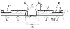
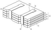
実施例1は積層された半導体チップの例である。図1は実施例1に係る半導体装置の斜視図、図2は図1のA−A断面図である。図1を参照に、回路が形成された半導体チップ10は複数積層されている。以後、半導体チップ10が4層に積層された例を示すが、本発明は、半導体チップ10が複数積層された半導体装置に適用することができる。半導体チップ10の上面にはパッド部18が形成されている。各半導体チップ10の側面には第2金属層24が形成されている。 Example 1 is an example of stacked semiconductor chips. 1 is a perspective view of a semiconductor device according to a first embodiment, and FIG. 2 is a cross-sectional view taken along line AA of FIG. Referring to FIG. 1, a plurality of
図2を参照に、各積層された半導体チップ10は半導体基板12と、半導体基板12の側面および上面に形成された第1絶縁層16を有する。半導体基板12上にはパッド電極14が設けられている。第1絶縁層16上および第1絶縁層16の側面に第1金属層20が設けられている。第1金属層20は第1絶縁層16に形成された開口部においてパッド電極14と電気的に接続しパッド部18を形成する。各半導体チップ10の間には、第2絶縁層22が設けられている。第2絶縁層22は上の半導体チップ10の半導体基板12と下の半導体チップ10上に設けられた第1金属層20とを電気的に分離している。各半導体チップ10の側面に設けられた第1金属層20を電気的に接続するように第2金属層24が設けられている。 Referring to FIG. 2, each
次に、図3(a)から図7(b)を用い、実施例1に係る半導体装置の製造方法について説明する。図3(a)から図4(b)は、図1の部分Bに相当する半導体チップ10を抜き出し、半導体ウェハ状態で製造される工程を示した斜視図である。図3(a)を参照に、シリコン半導体ウェハである半導体基板12上に例えばアルミニウムからなるパッド電極14が設けられている。パッド電極14は半導体基板12上に形成された回路パターンに電気的に接続されている。半導体基板12の上面に、半導体基板12を切断し半導体基板12を半導体チップに分割するためのスクライブラインを含むように第1溝部40を形成する。第1溝部40の深さは例えば50μm以上、幅は例えば約100μmとする。図3(b)を参照に、例えば感光性のポリイミド膜15を、スピンコート法を用い、半導体基板12の上面および第1溝部40の側面を覆うように形成する。ポリイミド膜15の膜厚は、半導体基板12上で例えば10μmである。 Next, a method for manufacturing the semiconductor device according to the first embodiment will be described with reference to FIGS. FIGS. 3A to 4B are perspective views showing a process of extracting the
図4(a)を参照に、感光性のポリイミド膜15に所定のパターンを露光し現像することにより、第1溝部40内に側面に凹部52を有する第2溝部42と、パッド電極14の上に開口部50を有する第1絶縁層16を形成する。凹部52は第1絶縁膜16の上面から第2溝部42の底面まで連続して形成されている。第2溝部42の深さは例えば50μm以上、第2溝部42の幅は例えば20μmである。凹部52の凹み量は例えば20μmである。図4(b)を参照に、第1絶縁層16の上面および凹部52の中央部に、例えば銅をメッキすることにより第1金属層20を形成する。 Referring to FIG. 4A, a predetermined pattern is exposed on the
図5(a)は、このときの上視図、図5(b)および図5(c)はそれぞれ図5(a)のC−CおよびD−D断面図である。図5(a)から図5(c)を参照に、第1絶縁層16に設けられた第2溝部42には凹部52が設けられている。凹部52の中央部に第1金属層20が形成されている。第1金属層20は、半導体基板12上に設けられたパッド電極14と開口部50で接続されている。 FIG. 5A is a top view at this time, and FIG. 5B and FIG. 5C are CC and DD sectional views of FIG. 5A, respectively. With reference to FIG. 5A to FIG. 5C, a
図6は図5(a)のD−D断面に相当する断面図である。図6を参照に、半導体基板12を背面より第2溝部42に達するように研磨する。このとき、半導体基板12の厚さを例えば50μmとする。第2溝部42の深さは例えば50μm以上のため、半導体基板12は第2溝部42により分割され、第1絶縁層16を有する半導体チップ10となる。なお、半導体基板12の厚さを薄くする工程は、研磨以外の方法であってもよい。 FIG. 6 is a cross-sectional view corresponding to the DD cross section of FIG. Referring to FIG. 6, the
図7(a)および図7(b)は図1の部分Bに相当する斜視図である。図7(a)を参照に、図6で分割された半導体チップ10を積層する。半導体チップ10の間には第2絶縁層22を挟み、各半導体チップ10は接着剤によりお互いに固着される。このとき、各半導体チップ10の凹部52は、積層された半導体チップ10の最上面から最下面に渡り連続して設けられた凹部52を構成する。第2絶縁層22は図6で背面を研磨する前に、第1金属層20上に形成しても良い。 FIG. 7A and FIG. 7B are perspective views corresponding to the portion B in FIG. Referring to FIG. 7A, the semiconductor chips 10 divided in FIG. 6 are stacked. The second insulating
図7(b)を参照に、各半導体チップ10の凹部52に例えば銀ペーストをスキージし埋め込み、第2金属層24を形成する。第2金属層24により、各半導体チップ10に設けられた第1金属層20が電気的に接続される。以上により実施例1に係る半導体装置が完成する。 Referring to FIG. 7B, the
実施例1において、積層される半導体チップ10は、同じ半導体チップであるとは限られない。例えば、半導体メモリ装置が形成された半導体チップとロジック回路が形成された半導体チップを積層することも可能である。積層された全ての半導体チップ10が全ての凹部52に形成された第2金属層24に接続するパッド電極14を有する必要はない。また、1つの半導体チップ10において、1つの第2金属層24に複数のパッド電極14が接続しても良い。各凹部52に対し、各半導体チップ10のいかなるパッド電極14を接続するかまたは接続しないかは、積層された半導体チップ30でいかなる機能を実現するかに応じ適宜選択することができる。さらに、実施例1では、各半導体チップ10が凹部52を有する第1絶縁層16、第1金属層20を有しているが、積層された複数の半導体チップのうち、少なくとも1つの半導体チップ10が凹部52を有する第1絶縁層16、第1金属層20を有していれば良い。 In the first embodiment, the stacked
図8のように、第2金属層24aの形成は、無電界メッキ法を用い例えば銅を形成してもよい。無電解メッキ法により第2金属を形成した場合、第1金属層20に形成されるメッキ層は、各半導体チップ10の各々の第1金属層20に厚みを持って形成される。よって、隙間を有する上下の半導体チップ10の各第1金属層20に形成されたメッキ層はお互いに接続し、第1金属層20に渡って形成される。よって、各半導体チップ10の第1金属層20間に隙間があって第1金属層20が電気的に接続されていない場合も無電解メッキ法を用いることにより、各第1金属層20が接続するように第2金属層24を形成することができる。 As shown in FIG. 8, the
実施例1に係る半導体装置においては、各半導体チップ10は半導体基板12の側面に第1絶縁層16を有している。第1絶縁層16は、半導体チップ10の上面と下面との間に連続的に設けられた凹部52を有している。凹部52内の側面の中央部には第1金属層20が設けられている。複数の半導体チップ10が積層された半導体装置は、各半導体チップ10の凹部52に、各半導体チップ10に設けられた第1金属層20を電気的に接続する第2金属層24が設けられている。 In the semiconductor device according to the first embodiment, each
各半導体チップ10に設けられた第1金属層20と第2金属層24とが接続することにより、第2金属層24を介し各半導体チップ10を接続することができる。従来例1のように、凹部52を半導体基板12に形成する場合、半導体基板12をエッチングする必要がある。しかし、実施例1では半導体基板12の側面に第1絶縁層16が設けられ、第1絶縁層16が凹部52を有している。よって、凹部52を簡単に形成することができる。第1金属層20が凹部52内の側面の中央部に設けられている。言い換えれば、第1金属層20は凹部52の側面に第1絶縁層16の上面に形成された第1金属層20と連続して形成され、かつ第2溝部42と接する領域には第1金属層20は形成されていない。第1金属層16がこのように設けられていることにより、従来例1および従来例2のように、スルーホールを切断する時に第1金属層20が剥がれることを防止することができる。また、凹部52が設けられているため、図7(b)のように凹部52に第2金属層24を例えば銀ペーストをスキージすることができ、簡単に第2金属層24を形成することがでできる。なお、積層された複数の半導体チップ30のうち、少なくとも1つの半導体チップ10が凹部52を有する第1絶縁層16、第1金属層20を有することにより、その半導体チップ10については上記効果を奏することができる。 By connecting the
また、第1絶縁層16は、半導体基板12の上面および側面に設けられている。これにより、第1絶縁層16をポリイミド膜15の塗布、露光現像法を用い簡単に形成することができる。 The first insulating
さらに、第1絶縁層16の上面に設けられた第1金属層20上に第2絶縁層22を有している。これにより、上の半導体チップ10と、第1金属層20とが電気的に接触することを防止することができる。第2絶縁層22は第1金属層20上に形成されていれば、上の半導体チップ10とのショートを防止する効果がある。しかし、下の半導体チップ10の上面に凹凸ができてしまうと、半導体チップ10間の熱抵抗が大きくなってしまう。よって、第2絶縁層22は半導体チップ10上面全面に渡り設けることが好ましい。 Furthermore, a second insulating
さらに、半導体チップ10は半導体基板12の上面に設けられたパッド電極14を有している。第1絶縁層16はパッド電極14の上に開口部50を有している。第1金属層20は、第1絶縁層16の上面にも設けられており、開口部50を介しパッド電極14と接続している。これにより、異なる半導体チップ10のパッド電極14同士を第2金属層24を介し接続することができる。 Further, the
実施例1に係る半導体装置の製造方法において、図3(a)のように、半導体ウェハである半導体基板12の上面に第1溝部40を形成する。図4(a)のように、半導体基板12の上面および第1溝部の側面を覆い、第1溝部40内に、側面に凹部52を有する第2溝部42を設けた第1絶縁層16を形成する。図4(b)のように、凹部52の側面に第1金属層16を形成する。図6のように、半導体基板12を背面より第2溝部42の底面に達するように除去することにより、半導体基板12を複数の半導体チップ10に分割する。このような製造方法により、スルーホールを形成する必要がない。よって、スルーホール形成のためのエッチングを行う必要がなく製造コストを削減することができる。半導体基板12の背面を除去することにより、金属層をダイシングで切断することなく半導体チップ10に分離することができる。よって、第1金属層20の剥がれることを防止することができる。 In the method for manufacturing a semiconductor device according to the first embodiment, as shown in FIG. 3A, a
また、第1絶縁層16を形成するために、図3(b)のように、半導体基板12の上面および第1溝部40の側面に、ポリイミド膜15(絶縁膜)を形成する。図4(a)のように、ポリイミド膜に凹部52を有する第2溝部42を形成する。このような工程により、スルーホールを形成することなく、簡単に第2溝部42および凹部52を形成することができる。なお、第1絶縁膜となるべき絶縁膜はポリイミド膜15以外の絶縁膜であってもよい。また、実施例1では、感光性ポリイミド膜15を用い、所定領域を露光することにより、第2溝部42および凹部52を形成しているが、第1絶縁膜となるべき絶縁膜上にフォトレジストを形成しエッチングにより第2溝部42および凹部52を形成してもよい。 Further, in order to form the first insulating
さらに、図4(a)のように、第1絶縁層16を形成する際には、半導体基板12上に設けられたパッド電極14の上に開口部50を有するように第1絶縁層16を形成する。図4(b)のように、第1金属層を形成する際は、第1絶縁層16の上面に、開口部50を介しパッド電極14と接続するように第1金属層20を形成する。このような工程により、第1金属層20を介し、半導体チップ10に形成された回路と第2金属層24とを電気的に接続することができる。 Further, as shown in FIG. 4A, when the first insulating
さらに、図4(b)のように、第1金属層20を形成する際は、凹部52内の側面の中央部に第1金属層20を形成している。第1金属層20は凹部52の全体に形成することもできるが、実施例1のように凹部52内の側面の中央部に第1金属層20を形成することにより、図7(b)のように、銀ペーストをスキージする際、第1金属層20に引っかかり、第1金属層が剥がれることを防止することができる。また、図8のように、無電解メッキ法を用い第2金属層24を形成する際、第1金属層20から成長したメッキ層が隣の凹部52の第1金属層20とショートすることを抑制することができる。 Further, as shown in FIG. 4B, when forming the
さらに、図7(a)のように、複数の半導体チップ10を積層する。図7(b)のように、複数の半導体チップ10の各第1金属層20を接続するように、凹部52に第2金属層24を形成する。これにより、各第1金属層20に接続する第2金属層24を形成する際、凹部52を有するため、銀ペーストをスキーズすることにより簡単に、凹部52に銀ペーストを埋め込むことができ第2金属層24を形成することができる。 Further, as shown in FIG. 7A, a plurality of
実施例2は、第1金属層20の上および第1絶縁層の側面に設けられ、側面に凹部を有する第2絶縁層を設けた半導体装置の例である。図9(a)から図12を用い、実施例2に係る半導体装置の製造方法について説明する。図9(a)から図10(b)は図3(a)と同様に半導体装置の部分Bに相当する斜視図である。図9(a)を参照に、実施例1の図3(a)および図3(b)の工程を行う。第1溝部40内に第2溝部42、パッド電極14上に開口部50を有する第1絶縁層16を形成する。第1溝部40および第2溝部42の幅は例えばそれぞれ100μmおよび40μmであり、第1溝部40および第2溝部42の深さは例えば50μm以上とする。また、第1絶縁層16の膜厚は例えば10μmである。図9(b)を参照に、第1絶縁層16上および側面に第1金属層20を形成する。第1金属層20は、開口部50において、パッド電極14と接続し、パッド部18を形成する。 Example 2 is an example of a semiconductor device in which a second insulating layer provided on the
図10(a)を参照に、第1絶縁層16の上面および第2溝部42の側面を覆い、第2溝部42内に、感光性のポリイミド膜27を例えば10μm塗布する。図10(b)を参照に、ポリイミド膜27の所定領域を露光し現像する。これにより、第2溝部42内の側面に凹部54を有する第3溝部44を形成する。第3溝部44の深さは例えば50μm以上、第3溝部44の幅は例えば20μmである。凹部54の凹み量は例えば20μmである。 Referring to FIG. 10A, the upper surface of the first insulating
図11(a)は、このときの上視図、図11(b)は図11(a)のE−E断面図である。図11(a)および図11(b)を参照に、凹部54内の側面の中央部に、第1絶縁膜16上および側面に形成された第1金属層20が露出するように凹部54が形成されている。第3溝部44の幅(例えば20μm)に両側の凹部54の凹み量(例えば2×20μm)を加えた幅が第2溝部42の幅(例えば40μm)より広いため、第1金属層20を凹部54内の側面に露出することができる。 FIG. 11A is a top view at this time, and FIG. 11B is an EE cross-sectional view of FIG. Referring to FIG. 11A and FIG. 11B, the
図12は図11(a)のE−E断面に相当する断面図である。図12を参照に、半導体基板12を背面より第3溝部44に達するように研磨する。このとき、半導体基板12の厚さを例えば50μmとする。第3溝部44の深さは例えば50μm以上のため、半導体基板12は第3溝部44で分割され、半導体チップ10となる。実施例1の図7(a)および図7(b)と同じ製造工程を行うことにより実施例2に係る半導体装置が完成する。 FIG. 12 is a cross-sectional view corresponding to the EE cross section of FIG. Referring to FIG. 12, the
実施例2は、実施例1に比べ、第1金属層20の上面および第1絶縁層16の側面に設けられ、側面に凹部54を有する第2絶縁層26を有している。さらに、第2金属層24は、各半導体チップ10に設けられた第1金属層20と凹部52で接続されている。第2絶縁層26により、上の半導体チップ10の半導体基板12と第1金属層20が電気的に接触することを防止することができる。また、第1絶縁層16の側面にも第2絶縁層26が設けられているため、第2絶縁層26を形成する際に、位置合わせ精度が悪いことに起因し、第2絶縁層26が第1金属層20を被覆しなくなることを防止することができる。なお、実施例1と同様に、積層された複数の半導体チップのうち、少なくとも1つの半導体チップ10が凹部52を有する第1絶縁層16、第1金属層20、第2絶縁層を有していれば良い。 Compared to the first embodiment, the second embodiment includes the second insulating
実施例2に係る半導体装置の製造方法において、図9(a)のように、半導体ウェハである半導体基板12の上面に第1溝部40を形成する。半導体基板12の上面および第1溝部40の側面を覆い、第1溝部40内に、第2溝部42を設けた第1絶縁層16を形成する。図9(b)のように、第1絶縁層16の上面に第1金属層20を形成する。図10(b)のように、第1絶縁層16の上面および第2溝部42の側面を覆い、第2溝部42内の側面に凹部54を有する第3溝部44を設け、凹部54内の側面に第1金属層20を露出するように第2絶縁層26を形成する。図12のように、半導体基板12を背面より第3溝部44の底面に達するように除去し、半導体基板12を複数の半導体チップ10に分割する。実施例1においては、第2絶縁層22と第1金属層20の位置合わせがずれることが起こりえる。例えば、第2絶縁層22が第1金属層20を適切に被覆していないと、第1金属層20と上の半導体基板12とがショートしてしまう。一方、第2絶縁膜が第1絶縁膜16の凹部52に設けられると、第2金属層24が形成し難くなる。実施例2の製造方法によれば、実施例1と同様な効果に加え、凹部54に暴露された第1金属層20以外の第1金属層20を第2絶縁層26が被覆できるため位置合わせずれに起因した第1金属層20と上の半導体基板12とがショートを防止することができる。 In the method of manufacturing a semiconductor device according to the second embodiment, as shown in FIG. 9A, the
さらに、第2絶縁層26を形成する際は、図10(a)のように、第1金属層20および第1絶縁層16上にポリイミド膜27(絶縁膜)を形成する。図10(b)のように、ポリイミド膜27に凹部54を有する第3溝部44を形成する。このような工程により、簡単に第2溝部44および凹部54を形成することができる。なお、第2絶縁膜となるべき絶縁膜はポリイミド膜27以外の絶縁膜であってもよい。また、第2絶縁膜となるべき絶縁膜上にフォトレジストを形成しエッチングにより第3溝部44および凹部54を形成してもよい。 Further, when the second insulating
実施例3から実施例5は積層された半導体チップ(内蔵半導体装置)をパッケージに実装した半導体装置の例である。図13を参照に、パッケージはガラスエポキシ樹脂からなるプリント基板32を有し、プリント基板32上に実施例1または実施例2の積層された半導体チップ30がハンダボール33によりフリップチップ実装されている。ハンダボール33は、例えば実施例1の図1の最上面の半導体チップ10のパッド部18に設けられている。プリント基板32の積層された半導体チップ30と反対の面にはハンダボール31が設けられている。ハンダボール31とハンダボール33とはプリント基板32の接続部(図示せず)により接続されている。 The third to fifth embodiments are examples of a semiconductor device in which stacked semiconductor chips (built-in semiconductor devices) are mounted on a package. Referring to FIG. 13, the package has a printed
図14を参照に、パッケージはプリント基板32およびエポキシ樹脂35を有し、プリント基板32に積層された半導体チップ30(内蔵半導体装置)がフェースアップで実装されている。ワイヤ34により、プリント基板32と半導体チップ30とが接続されている。ワイヤ34は例えば実施例1の図1の最上面の半導体チップ10のパッド部18に接続している。積層された半導体チップ30はエポキシ樹脂35により封止されている。実施例3および実施例4において、積層された半導体チップが実装されるのはプリント基板32であるが、絶縁基板に導電性の配線の形成された基板であればよい。 Referring to FIG. 14, the package includes a printed
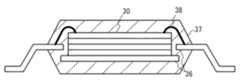
図15を参照に、パッケージはリードフレーム36およびエポキシ樹脂37を有し、積層された半導体チップ30(内蔵半導体装置)はリードフレーム36に実装され、リードフレーム36と積層された半導体チップ30とはワイヤ38で接続されている。積層された半導体チップ30は例えばエポキシ樹脂37により樹脂封止されている。実施例3から実施例5のように、実施例1または実施例2に係る積層された半導体チップ30(内蔵半導体装置)がパッケージに実装された半導体装置とすることもできる。 Referring to FIG. 15, the package includes a
実施例1および実施例2において、第1絶縁層16および第2絶縁層26はポリイミド膜からなる絶縁膜であったが、絶縁性の膜であればポリイド膜には限られない。例えば酸化シリコン膜等の無機膜、または有機膜を用いることもできる。第1金属層20はメッキ法で形成した銅であったが、金属層であればこれに限られない。例えばアルミニウムや金を用いることもできる。第2金属層24は銀ペーストや無電解メッキで形成された金属の例であったが、金属層であればこれらに限られない。例えば、金、銅等を用いることもできる。 In the first and second embodiments, the first insulating
以上、本発明の好ましい実施例について詳述したが、本発明は係る特定の実施例に限定されるものではなく、特許請求の範囲に記載された本発明の要旨の範囲内において、種々の変形・変更が可能である。
The preferred embodiments of the present invention have been described in detail above, but the present invention is not limited to such specific embodiments, and various modifications can be made within the scope of the gist of the present invention described in the claims.・ Change is possible.
Claims (18)
Translated fromJapanese前記凹部に設けられ、前記半導体チップに設けられた前記第1金属層を接続する第2金属層と、を具備する半導体装置。At least one semiconductor chip is provided on asemiconductor substrate, a first insulating layer provided on a sidesurface from theupper surface of thesemiconductor substrate and having a recessonthe sidesurface of the semiconductor substrate, and a central portionof the side surface in the recess A plurality of stacked semiconductor chips having a first metal layer providedon the first insulating layer;
A semiconductor device comprising: a second metal layer provided in the recess and connecting the first metal layer provided in the semiconductor chip.
前記第1金属層の上面に設けられた第2絶縁層を具備する請求項2記載の半導体装置。The first metal layer is provided on an upper surface of the first insulating layer;
The semiconductor device according to claim 2, further comprising a second insulating layer provided on an upper surface of the first metal layer.
前記凹部に設けられ、前記半導体チップに設けられた前記第1金属層と前記凹部で接続される第2金属層と、を具備する半導体装置。At least one semiconductor chip includes a semiconductor substrate, a first insulating layer provided on a side surface and an upper surface of the semiconductor substrate, a first metal layer provided on a side surface and an upper surface of the first insulating layer, and the first A plurality of stacked semiconductor chips having a second insulating layer provided on the upper surface of the metal layer and the side surface of the first insulating layer and having a recess on the side surface;
A semiconductor device comprising: the first metal layer provided in the concave portion and provided in the semiconductor chip; and a second metal layer connected by the concave portion.
前記第1絶縁層は前記パッド電極の上に開口部を有し、
前記第1金属層は、前記第1絶縁膜層の上面にも設けられ、前記開口部を介し前記パッドと接続する請求項1から4のいずれか一項記載の半導体装置。The semiconductor chip has a pad electrode provided on a semiconductor substrate,
The first insulating layer has an opening on the pad electrode;
5. The semiconductor device according to claim 1, wherein the first metal layer is also provided on an upper surface of the first insulating film layer, and is connected to the pad through the opening.
前記半導体ウェハの上面および前記第1溝部の側面を覆い、前記第1溝部内に、側面に凹部を有する第2溝部を有する第1絶縁層を形成する工程と、
前記凹部の側面に第1金属層を形成する工程と、
前記半導体ウェハを背面より前記第2溝部の底面に達するように除去し、前記半導体ウェハを複数の半導体チップに分割する工程と、を有する半導体装置の製造方法。Forming a first groove on the upper surface of the semiconductor wafer;
Forming a first insulating layer that covers a top surface of the semiconductor wafer and a side surface of the first groove portion, and has a second groove portion having a recess on the side surface in the first groove portion;
Forming a first metal layer on a side surface of the recess;
Removing the semiconductor wafer from the back surface so as to reach the bottom surface of the second groove, and dividing the semiconductor wafer into a plurality of semiconductor chips.
前記半導体ウェハの上面に、絶縁膜を形成する工程と、
前記絶縁膜に前記凹部を有する前記第2溝部を形成する工程と、を含む請求項10記載の半導体装置の製造方法。The step of forming the first insulating layer includes:
Forming an insulating film on the upper surface of the semiconductor wafer;
The method of manufacturing a semiconductor device according to claim 10, further comprising: forming the second groove portion having the recess in the insulating film.
前記第1金属層を形成する工程は、前記第1絶縁膜層の上面に、前記開口部を介し前記パッド電極と接続する前記第1金属層を形成する工程を含む請求項10または11記載の半導体装置の製造方法。Forming the first insulating layer includes forming the first insulating layer having an opening on a pad electrode provided on the semiconductor wafer;
12. The step of forming the first metal layer includes a step of forming the first metal layer connected to the pad electrode through the opening on the upper surface of the first insulating film layer. A method for manufacturing a semiconductor device.
前記第1金属層の上面に第2絶縁層を形成する工程を有する請求項10から12のいずれか一項記載の半導体装置の製造方法。Forming the first metal layer includes forming the first metal layer on an upper surface of the first insulating layer;
The method for manufacturing a semiconductor device according to claim 10, further comprising a step of forming a second insulating layer on an upper surface of the first metal layer.
前記半導体ウェハの上面および前記第1溝部の側面を覆い、前記第1溝部内に、第2溝部を設けた第1絶縁層を形成する工程と、
前記第1絶縁層の上面および側面に第1金属層を形成する工程と、
前記第1絶縁層の上面および前記第2溝部の側面を覆い、前記第2溝部内に側面に凹部を有する第3溝部を有し、前記凹部内に前記第1金属層が露出するように第2絶縁層を形成する工程と、
前記半導体ウェハを背面より前記第3溝部の底面に達するように除去し、前記半導体ウェハを複数の半導体チップに分割する工程と、を有する半導体装置の製造方法。Forming a first groove on the upper surface of the semiconductor wafer;
Forming a first insulating layer that covers an upper surface of the semiconductor wafer and a side surface of the first groove, and a second groove is provided in the first groove;
Forming a first metal layer on top and side surfaces of the first insulating layer;
A third groove portion that covers the upper surface of the first insulating layer and the side surface of the second groove portion, has a recess in the side surface in the second groove portion, and is exposed so that the first metal layer is exposed in the recess. Forming two insulating layers;
Removing the semiconductor wafer from the back surface so as to reach the bottom surface of the third groove, and dividing the semiconductor wafer into a plurality of semiconductor chips.
前記半導体ウェハ上に、絶縁膜を形成する工程と、
前記絶縁膜に前記凹部を有する第3溝部を形成する工程と、を含む請求項15記載の半導体装置の製造方法。The step of forming the second insulating layer includes:
Forming an insulating film on the semiconductor wafer;
The method of manufacturing a semiconductor device according to claim 15, further comprising: forming a third groove portion having the recess in the insulating film.
前記第1金属層を接続するように、前記凹部に第2金属層を形成する工程と、を有する請求項10から16のいずれか一項記載の半導体装置の製造方法。Laminating a plurality of semiconductor chips including at least one semiconductor chip divided from the semiconductor wafer;
The method of manufacturing a semiconductor device according to claim 10, further comprising: forming a second metal layer in the recess so as to connect the first metal layer.
Applications Claiming Priority (1)
| Application Number | Priority Date | Filing Date | Title |
|---|---|---|---|
| PCT/JP2005/022646WO2007066409A1 (en) | 2005-12-09 | 2005-12-09 | Semiconductor device and its manufacturing method |
Publications (2)
| Publication Number | Publication Date |
|---|---|
| JPWO2007066409A1 JPWO2007066409A1 (en) | 2009-05-14 |
| JP4934053B2true JP4934053B2 (en) | 2012-05-16 |
Family
ID=38122562
Family Applications (1)
| Application Number | Title | Priority Date | Filing Date |
|---|---|---|---|
| JP2007549007AExpired - Fee RelatedJP4934053B2 (en) | 2005-12-09 | 2005-12-09 | Semiconductor device and manufacturing method thereof |
Country Status (4)
| Country | Link |
|---|---|
| US (3) | US7605457B2 (en) |
| JP (1) | JP4934053B2 (en) |
| TW (1) | TWI348741B (en) |
| WO (1) | WO2007066409A1 (en) |
Families Citing this family (44)
| Publication number | Priority date | Publication date | Assignee | Title |
|---|---|---|---|---|
| JP4934053B2 (en)* | 2005-12-09 | 2012-05-16 | スパンション エルエルシー | Semiconductor device and manufacturing method thereof |
| US7901989B2 (en) | 2006-10-10 | 2011-03-08 | Tessera, Inc. | Reconstituted wafer level stacking |
| US7829438B2 (en) | 2006-10-10 | 2010-11-09 | Tessera, Inc. | Edge connect wafer level stacking |
| US8513789B2 (en) | 2006-10-10 | 2013-08-20 | Tessera, Inc. | Edge connect wafer level stacking with leads extending along edges |
| US7952195B2 (en) | 2006-12-28 | 2011-05-31 | Tessera, Inc. | Stacked packages with bridging traces |
| KR100891529B1 (en)* | 2007-07-27 | 2009-04-03 | 주식회사 하이닉스반도체 | Semiconductor package, manufacturing method thereof |
| JP5572089B2 (en) | 2007-07-27 | 2014-08-13 | テッセラ,インコーポレイテッド | Reconfigured wafer stack packaging with pad extension after application |
| US8551815B2 (en)* | 2007-08-03 | 2013-10-08 | Tessera, Inc. | Stack packages using reconstituted wafers |
| US8043895B2 (en) | 2007-08-09 | 2011-10-25 | Tessera, Inc. | Method of fabricating stacked assembly including plurality of stacked microelectronic elements |
| JP2009188234A (en)* | 2008-02-07 | 2009-08-20 | Minami Kk | Method of stacking semiconductors, and semiconductor package using semiconductor stacked by the method |
| JP5174518B2 (en)* | 2008-04-17 | 2013-04-03 | スパンション エルエルシー | Stacked semiconductor device and manufacturing method thereof |
| JP5639052B2 (en) | 2008-06-16 | 2014-12-10 | テッセラ,インコーポレイテッド | Edge stacking at wafer level |
| US7846772B2 (en)* | 2008-06-23 | 2010-12-07 | Headway Technologies, Inc. | Layered chip package and method of manufacturing same |
| US7745259B2 (en)* | 2008-06-30 | 2010-06-29 | Headway Technologies, Inc. | Layered chip package and method of manufacturing same |
| US7829988B2 (en)* | 2008-09-22 | 2010-11-09 | Fairchild Semiconductor Corporation | Stacking quad pre-molded component packages, systems using the same, and methods of making the same |
| JP5112275B2 (en)* | 2008-12-16 | 2013-01-09 | 新光電気工業株式会社 | Semiconductor device and manufacturing method of semiconductor device |
| US8274165B2 (en)* | 2009-02-10 | 2012-09-25 | Headway Technologies, Inc. | Semiconductor substrate, laminated chip package, semiconductor plate and method of manufacturing the same |
| WO2010104610A2 (en)* | 2009-03-13 | 2010-09-16 | Tessera Technologies Hungary Kft. | Stacked microelectronic assemblies having vias extending through bond pads |
| US20100270668A1 (en)* | 2009-04-28 | 2010-10-28 | Wafer-Level Packaging Portfolio Llc | Dual Interconnection in Stacked Memory and Controller Module |
| US8569878B2 (en)* | 2009-10-22 | 2013-10-29 | Headway Technologies, Inc. | Semiconductor substrate, laminated chip package, semiconductor plate and method of manufacturing the same |
| US8525167B2 (en)* | 2009-10-26 | 2013-09-03 | Headway Technologies, Inc. | Laminated chips package, semiconductor substrate and method of manufacturing the laminated chips package |
| US7902677B1 (en)* | 2009-10-28 | 2011-03-08 | Headway Technologies, Inc. | Composite layered chip package and method of manufacturing same |
| TW201214656A (en)* | 2010-09-27 | 2012-04-01 | Universal Scient Ind Shanghai | Chip stacked structure and method of fabricating the same |
| US8652877B2 (en)* | 2010-12-06 | 2014-02-18 | Headway Technologies, Inc. | Method of manufacturing layered chip package |
| DE102011010248B3 (en)* | 2011-02-03 | 2012-07-12 | Infineon Technologies Ag | Method for manufacturing power semiconductor device e.g. insulated gate bipolar transistor, involves forming trenches partially filled with insulating material starting from side to side in regions of semiconductor structure |
| US8587088B2 (en)* | 2011-02-17 | 2013-11-19 | Apple Inc. | Side-mounted controller and methods for making the same |
| KR20130027628A (en)* | 2011-06-27 | 2013-03-18 | 삼성전자주식회사 | Stacked semiconductor device |
| TWI509678B (en)* | 2011-07-27 | 2015-11-21 | Inpaq Technology Co Ltd | Planar semiconductor device and manufacturing method thereof |
| FR2993101B1 (en)* | 2012-07-06 | 2015-07-17 | Commissariat Energie Atomique | METHOD FOR ASSEMBLING AND ENCAPSULATING LITHIUM MICROBATTERIES AND MICROBATTERIES THUS OBTAINED |
| US9299670B2 (en) | 2013-03-14 | 2016-03-29 | Freescale Semiconductor, Inc. | Stacked microelectronic packages having sidewall conductors and methods for the fabrication thereof |
| US9524950B2 (en) | 2013-05-31 | 2016-12-20 | Freescale Semiconductor, Inc. | Stacked microelectronic packages having sidewall conductors and methods for the fabrication thereof |
| US9305911B2 (en)* | 2013-12-05 | 2016-04-05 | Freescale Semiconductor, Inc. | Devices and stacked microelectronic packages with package surface conductors and adjacent trenches and methods of their fabrication |
| US10388607B2 (en) | 2014-12-17 | 2019-08-20 | Nxp Usa, Inc. | Microelectronic devices with multi-layer package surface conductors and methods of their fabrication |
| CN106298631B (en)* | 2015-05-12 | 2020-07-14 | 联华电子股份有限公司 | Semiconductor element and manufacturing method thereof |
| CN106252241B (en)* | 2016-09-08 | 2019-03-05 | 华进半导体封装先导技术研发中心有限公司 | The manufacture craft of chip package side wall pad or salient point |
| CN106206423B (en)* | 2016-09-08 | 2019-01-04 | 华进半导体封装先导技术研发中心有限公司 | Chip package side wall plants ball technique |
| CN107993997B (en)* | 2016-10-26 | 2020-06-16 | 晟碟信息科技(上海)有限公司 | Semiconductor device with a plurality of transistors |
| CN107994011B (en)* | 2016-10-26 | 2020-06-02 | 晟碟信息科技(上海)有限公司 | Semiconductor package and method of manufacturing the same |
| JP6926645B2 (en)* | 2017-05-08 | 2021-08-25 | 株式会社デンソー | Semiconductor devices and their manufacturing methods |
| US10319802B1 (en)* | 2017-11-22 | 2019-06-11 | Microsoft Technology Licensing, Llc | Display substrate edge patterning and metallization |
| CN110010495B (en)* | 2018-12-26 | 2021-05-28 | 浙江集迈科微电子有限公司 | High-density side wall interconnection method |
| CN110010494B (en)* | 2018-12-26 | 2021-04-06 | 浙江集迈科微电子有限公司 | Method for manufacturing system-in-package interconnection structure with side wall provided with bonding pad |
| US11715696B2 (en) | 2021-04-22 | 2023-08-01 | Micron Technology, Inc. | Semiconductor devices with recessed pads for die stack interconnections |
| US11646269B2 (en)* | 2021-04-28 | 2023-05-09 | Micron Technology, Inc. | Recessed semiconductor devices, and associated systems and methods |
Citations (5)
| Publication number | Priority date | Publication date | Assignee | Title |
|---|---|---|---|---|
| JPH065665A (en)* | 1992-04-20 | 1994-01-14 | Mitsubishi Heavy Ind Ltd | Method for forming electrode on side face of ic chip and multi-ic chip |
| JPH0883888A (en)* | 1994-09-06 | 1996-03-26 | Internatl Business Mach Corp <Ibm> | Formation of integrated circuit chip,integrated circuit chip,electronic module and formation of electronic module |
| JP2001210782A (en)* | 2000-01-27 | 2001-08-03 | Seiko Epson Corp | Semiconductor chip, multi-chip package, semiconductor device, and electronic device using the same |
| JP2002076167A (en)* | 2000-08-29 | 2002-03-15 | Sony Corp | Semiconductor chip, stacked semiconductor package and their manufacturing method |
| JP2004221372A (en)* | 2003-01-16 | 2004-08-05 | Seiko Epson Corp | Semiconductor device, semiconductor module, electronic device, method of manufacturing semiconductor device, and method of manufacturing semiconductor module |
Family Cites Families (23)
| Publication number | Priority date | Publication date | Assignee | Title |
|---|---|---|---|---|
| JP2809115B2 (en)* | 1993-10-13 | 1998-10-08 | ヤマハ株式会社 | Semiconductor device and manufacturing method thereof |
| US5466634A (en)* | 1994-12-20 | 1995-11-14 | International Business Machines Corporation | Electronic modules with interconnected surface metallization layers and fabrication methods therefore |
| US5648684A (en)* | 1995-07-26 | 1997-07-15 | International Business Machines Corporation | Endcap chip with conductive, monolithic L-connect for multichip stack |
| US5888884A (en)* | 1998-01-02 | 1999-03-30 | General Electric Company | Electronic device pad relocation, precision placement, and packaging in arrays |
| US6624505B2 (en)* | 1998-02-06 | 2003-09-23 | Shellcase, Ltd. | Packaged integrated circuits and methods of producing thereof |
| US6335225B1 (en)* | 1998-02-20 | 2002-01-01 | Micron Technology, Inc. | High density direct connect LOC assembly |
| US6180881B1 (en)* | 1998-05-05 | 2001-01-30 | Harlan Ruben Isaak | Chip stack and method of making same |
| US6180506B1 (en)* | 1998-09-14 | 2001-01-30 | International Business Machines Corporation | Upper redundant layer for damascene metallization |
| JP2001085361A (en)* | 1999-09-10 | 2001-03-30 | Oki Electric Ind Co Ltd | Semiconductor device and manufacturing method |
| JP3800910B2 (en) | 2000-03-07 | 2006-07-26 | セイコーエプソン株式会社 | SEMICONDUCTOR DEVICE, ITS MANUFACTURING METHOD, AND ELECTRONIC DEVICE |
| US6747348B2 (en)* | 2001-10-16 | 2004-06-08 | Micron Technology, Inc. | Apparatus and method for leadless packaging of semiconductor devices |
| KR100486832B1 (en)* | 2002-02-06 | 2005-05-03 | 삼성전자주식회사 | Semiconductor Chip, Chip Stack Package And Manufacturing Method |
| TWI232560B (en)* | 2002-04-23 | 2005-05-11 | Sanyo Electric Co | Semiconductor device and its manufacture |
| SG107595A1 (en)* | 2002-06-18 | 2004-12-29 | Micron Technology Inc | Semiconductor devices and semiconductor device components with peripherally located, castellated contacts, assembles and packages including such semiconductor devices or packages and associated methods |
| US6855572B2 (en)* | 2002-08-28 | 2005-02-15 | Micron Technology, Inc. | Castellation wafer level packaging of integrated circuit chips |
| JP4081666B2 (en)* | 2002-09-24 | 2008-04-30 | セイコーエプソン株式会社 | Semiconductor device and manufacturing method thereof, circuit board, and electronic apparatus |
| JP4248928B2 (en)* | 2003-05-13 | 2009-04-02 | ローム株式会社 | Semiconductor chip manufacturing method, semiconductor device manufacturing method, semiconductor chip, and semiconductor device |
| JP2004342861A (en) | 2003-05-16 | 2004-12-02 | Sony Corp | Chip type electronic component, dummy wafer, methods of manufacturing them, and packaging structure of electronic component |
| SG120123A1 (en)* | 2003-09-30 | 2006-03-28 | Micron Technology Inc | Castellated chip-scale packages and methods for fabricating the same |
| KR100604903B1 (en)* | 2004-09-30 | 2006-07-28 | 삼성전자주식회사 | Semiconductor wafer with improved step coverage and manufacturing method |
| JP4934053B2 (en) | 2005-12-09 | 2012-05-16 | スパンション エルエルシー | Semiconductor device and manufacturing method thereof |
| WO2008047416A1 (en)* | 2006-10-18 | 2008-04-24 | Spansion Llc | Voltage detecting circuit |
| US7585750B2 (en)* | 2007-05-04 | 2009-09-08 | Stats Chippac, Ltd. | Semiconductor package having through-hole via on saw streets formed with partial saw |
- 2005
- 2005-12-09JPJP2007549007Apatent/JP4934053B2/ennot_activeExpired - Fee Related
- 2005-12-09WOPCT/JP2005/022646patent/WO2007066409A1/enactiveApplication Filing
- 2006
- 2006-12-06TWTW095145292Apatent/TWI348741B/ennot_activeIP Right Cessation
- 2006-12-07USUS11/636,155patent/US7605457B2/ennot_activeExpired - Fee Related
- 2009
- 2009-09-09USUS12/556,408patent/US8030179B2/ennot_activeExpired - Fee Related
- 2011
- 2011-10-04USUS13/252,714patent/US9293441B2/ennot_activeExpired - Fee Related
Patent Citations (5)
| Publication number | Priority date | Publication date | Assignee | Title |
|---|---|---|---|---|
| JPH065665A (en)* | 1992-04-20 | 1994-01-14 | Mitsubishi Heavy Ind Ltd | Method for forming electrode on side face of ic chip and multi-ic chip |
| JPH0883888A (en)* | 1994-09-06 | 1996-03-26 | Internatl Business Mach Corp <Ibm> | Formation of integrated circuit chip,integrated circuit chip,electronic module and formation of electronic module |
| JP2001210782A (en)* | 2000-01-27 | 2001-08-03 | Seiko Epson Corp | Semiconductor chip, multi-chip package, semiconductor device, and electronic device using the same |
| JP2002076167A (en)* | 2000-08-29 | 2002-03-15 | Sony Corp | Semiconductor chip, stacked semiconductor package and their manufacturing method |
| JP2004221372A (en)* | 2003-01-16 | 2004-08-05 | Seiko Epson Corp | Semiconductor device, semiconductor module, electronic device, method of manufacturing semiconductor device, and method of manufacturing semiconductor module |
Also Published As
| Publication number | Publication date |
|---|---|
| WO2007066409A1 (en) | 2007-06-14 |
| US7605457B2 (en) | 2009-10-20 |
| JPWO2007066409A1 (en) | 2009-05-14 |
| US8030179B2 (en) | 2011-10-04 |
| TWI348741B (en) | 2011-09-11 |
| US20090325346A1 (en) | 2009-12-31 |
| TW200733275A (en) | 2007-09-01 |
| US20120025364A1 (en) | 2012-02-02 |
| US20070145579A1 (en) | 2007-06-28 |
| US9293441B2 (en) | 2016-03-22 |
Similar Documents
| Publication | Publication Date | Title |
|---|---|---|
| JP4934053B2 (en) | Semiconductor device and manufacturing method thereof | |
| JP4361820B2 (en) | Wafer level package, multi-stacked package, and manufacturing method thereof | |
| US20090134528A1 (en) | Semiconductor package, electronic device including the semiconductor package, and method of manufacturing the semiconductor package | |
| KR100871709B1 (en) | Chip stack package and manufacturing method thereof | |
| KR20180130043A (en) | Semiconductor package with chip stacks | |
| US20070262434A1 (en) | Interconnected ic packages with vertical smt pads | |
| US8294251B2 (en) | Stacked semiconductor package with localized cavities for wire bonding | |
| KR102589736B1 (en) | Semiconductor chip and Semiconductor package including the same | |
| JP2005327984A (en) | Electronic component and method of manufacturing electronic-component mounting structure | |
| KR20200024499A (en) | Stack package include bridge die | |
| JP2008311599A (en) | Molded reconfigured wafer, stack package using the same, and method for manufacturing the stack package | |
| US10448508B2 (en) | Printed circuit board and semiconductor package including the same | |
| KR20120000690A (en) | Semiconductor device and manufacturing method thereof | |
| TWI556379B (en) | Semiconductor package and manufacturing method thereof | |
| US10957658B2 (en) | Package structure with structure reinforcing element and manufacturing method thereof | |
| US8470640B2 (en) | Method of fabricating stacked semiconductor package with localized cavities for wire bonding | |
| KR20210145568A (en) | Semiconductor devices including stacked substrates and method for fabricating the same | |
| KR20170094026A (en) | Semiconductor chip having through electrode, chip stack structure including the same and method of manufacturing semiconductor chip | |
| KR20130123725A (en) | Stacked semiconductor package and method for manufacturing the same | |
| US8294250B2 (en) | Wiring substrate for a semiconductor chip, and semiconducotor package having the wiring substrate | |
| US20080142945A1 (en) | Semiconductor package with redistribution layer of semiconductor chip directly contacted with substrate and method of fabricating the same | |
| KR20110080859A (en) | Manufacturing method of semiconductor package | |
| JP4334397B2 (en) | Semiconductor device and manufacturing method thereof | |
| US10115704B2 (en) | Semiconductor device | |
| KR102809407B1 (en) | Semiconductor package |
Legal Events
| Date | Code | Title | Description |
|---|---|---|---|
| RD04 | Notification of resignation of power of attorney | Free format text:JAPANESE INTERMEDIATE CODE: A7424 Effective date:20100303 | |
| RD03 | Notification of appointment of power of attorney | Free format text:JAPANESE INTERMEDIATE CODE: A7423 Effective date:20100616 | |
| RD03 | Notification of appointment of power of attorney | Free format text:JAPANESE INTERMEDIATE CODE: A7423 Effective date:20100805 | |
| A711 | Notification of change in applicant | Free format text:JAPANESE INTERMEDIATE CODE: A711 Effective date:20100922 | |
| A131 | Notification of reasons for refusal | Free format text:JAPANESE INTERMEDIATE CODE: A131 Effective date:20110809 | |
| A521 | Request for written amendment filed | Free format text:JAPANESE INTERMEDIATE CODE: A523 Effective date:20111108 | |
| TRDD | Decision of grant or rejection written | ||
| A01 | Written decision to grant a patent or to grant a registration (utility model) | Free format text:JAPANESE INTERMEDIATE CODE: A01 Effective date:20120124 | |
| A01 | Written decision to grant a patent or to grant a registration (utility model) | Free format text:JAPANESE INTERMEDIATE CODE: A01 | |
| A61 | First payment of annual fees (during grant procedure) | Free format text:JAPANESE INTERMEDIATE CODE: A61 Effective date:20120217 | |
| R150 | Certificate of patent or registration of utility model | Free format text:JAPANESE INTERMEDIATE CODE: R150 | |
| FPAY | Renewal fee payment (event date is renewal date of database) | Free format text:PAYMENT UNTIL: 20150224 Year of fee payment:3 | |
| FPAY | Renewal fee payment (event date is renewal date of database) | Free format text:PAYMENT UNTIL: 20150224 Year of fee payment:3 | |
| RD02 | Notification of acceptance of power of attorney | Free format text:JAPANESE INTERMEDIATE CODE: R3D02 | |
| FPAY | Renewal fee payment (event date is renewal date of database) | Free format text:PAYMENT UNTIL: 20150224 Year of fee payment:3 | |
| R250 | Receipt of annual fees | Free format text:JAPANESE INTERMEDIATE CODE: R250 | |
| S111 | Request for change of ownership or part of ownership | Free format text:JAPANESE INTERMEDIATE CODE: R313111 | |
| R350 | Written notification of registration of transfer | Free format text:JAPANESE INTERMEDIATE CODE: R350 | |
| R250 | Receipt of annual fees | Free format text:JAPANESE INTERMEDIATE CODE: R250 | |
| R250 | Receipt of annual fees | Free format text:JAPANESE INTERMEDIATE CODE: R250 | |
| LAPS | Cancellation because of no payment of annual fees |