JP4933687B2 - Composite memory material comprising a mixture of phase change memory material and dielectric material - Google Patents
Composite memory material comprising a mixture of phase change memory material and dielectric materialDownload PDFInfo
- Publication number
- JP4933687B2 JP4933687B2JP51979498AJP51979498AJP4933687B2JP 4933687 B2JP4933687 B2JP 4933687B2JP 51979498 AJP51979498 AJP 51979498AJP 51979498 AJP51979498 AJP 51979498AJP 4933687 B2JP4933687 B2JP 4933687B2
- Authority
- JP
- Japan
- Prior art keywords
- memory
- phase change
- twenty
- memory material
- group
- Prior art date
- Legal status (The legal status is an assumption and is not a legal conclusion. Google has not performed a legal analysis and makes no representation as to the accuracy of the status listed.)
- Expired - Lifetime
Links
- 230000015654memoryEffects0.000titleclaimsdescription183
- 239000000463materialSubstances0.000titleclaimsdescription159
- 239000000203mixtureSubstances0.000titleclaimsdescription55
- 230000008859changeEffects0.000titleclaimsdescription51
- 239000002131composite materialSubstances0.000titleclaimsdescription37
- 239000003989dielectric materialSubstances0.000titleclaimsdescription32
- 239000000956alloySubstances0.000claimsdescription26
- 229910045601alloyInorganic materials0.000claimsdescription26
- 229910052723transition metalInorganic materials0.000claimsdescription21
- 229910052719titaniumInorganic materials0.000claimsdescription17
- 229910052710siliconInorganic materials0.000claimsdescription11
- 229910052714telluriumInorganic materials0.000claimsdescription11
- 229910052721tungstenInorganic materials0.000claimsdescription10
- 229910052804chromiumInorganic materials0.000claimsdescription9
- 229910052758niobiumInorganic materials0.000claimsdescription9
- 229910052760oxygenInorganic materials0.000claimsdescription8
- 229910052787antimonyInorganic materials0.000claimsdescription7
- 229910052711seleniumInorganic materials0.000claimsdescription7
- 229910052799carbonInorganic materials0.000claimsdescription6
- 229910052732germaniumInorganic materials0.000claimsdescription6
- 229910052742ironInorganic materials0.000claimsdescription5
- 229910052759nickelInorganic materials0.000claimsdescription5
- 150000004767nitridesChemical class0.000claimsdescription5
- 229910052763palladiumInorganic materials0.000claimsdescription5
- 229910052698phosphorusInorganic materials0.000claimsdescription5
- 229910052697platinumInorganic materials0.000claimsdescription5
- 229910052715tantalumInorganic materials0.000claimsdescription5
- 229910052718tinInorganic materials0.000claimsdescription5
- OKTJSMMVPCPJKN-UHFFFAOYSA-NCarbonChemical compound[C]OKTJSMMVPCPJKN-UHFFFAOYSA-N0.000claimsdescription4
- 229910052785arsenicInorganic materials0.000claimsdescription4
- 229910052797bismuthInorganic materials0.000claimsdescription4
- 229910052735hafniumInorganic materials0.000claimsdescription4
- 239000008241heterogeneous mixtureSubstances0.000claimsdescription4
- 229910052745leadInorganic materials0.000claimsdescription4
- 229910052750molybdenumInorganic materials0.000claimsdescription4
- 229910052717sulfurInorganic materials0.000claimsdescription4
- 229910052720vanadiumInorganic materials0.000claimsdescription4
- 229910052726zirconiumInorganic materials0.000claimsdescription4
- 150000001805chlorine compoundsChemical class0.000claimsdescription3
- 150000002222fluorine compoundsChemical class0.000claimsdescription3
- 150000001247metal acetylidesChemical class0.000claimsdescription3
- 150000003568thioethersChemical class0.000claims2
- 230000008878couplingEffects0.000claims1
- 238000010168coupling processMethods0.000claims1
- 238000005859coupling reactionMethods0.000claims1
- 238000003860storageMethods0.000description21
- 239000013078crystalSubstances0.000description20
- 239000010409thin filmSubstances0.000description19
- 239000011159matrix materialSubstances0.000description15
- 238000000034methodMethods0.000description15
- 239000010936titaniumSubstances0.000description15
- 150000003624transition metalsChemical class0.000description11
- 238000002955isolationMethods0.000description10
- 239000012782phase change materialSubstances0.000description10
- 239000004065semiconductorSubstances0.000description10
- 229910005936Ge—SbInorganic materials0.000description9
- 229910052757nitrogenInorganic materials0.000description9
- 239000000758substrateSubstances0.000description8
- RTAQQCXQSZGOHL-UHFFFAOYSA-NTitaniumChemical compound[Ti]RTAQQCXQSZGOHL-UHFFFAOYSA-N0.000description7
- 229910052798chalcogenInorganic materials0.000description7
- 150000001787chalcogensChemical class0.000description7
- IJGRMHOSHXDMSA-UHFFFAOYSA-NnitrogenSubstancesN#NIJGRMHOSHXDMSA-UHFFFAOYSA-N0.000description7
- 230000008569processEffects0.000description7
- 239000007787solidSubstances0.000description7
- 238000004544sputter depositionMethods0.000description6
- 229910052782aluminiumInorganic materials0.000description5
- 150000004770chalcogenidesChemical class0.000description5
- 150000001875compoundsChemical class0.000description5
- 239000000470constituentSubstances0.000description5
- 230000006870functionEffects0.000description5
- 238000001459lithographyMethods0.000description5
- 239000011148porous materialSubstances0.000description5
- 239000004952PolyamideSubstances0.000description4
- 230000015572biosynthetic processEffects0.000description4
- 238000000151depositionMethods0.000description4
- 230000004048modificationEffects0.000description4
- 238000012986modificationMethods0.000description4
- 229920002647polyamidePolymers0.000description4
- UFHFLCQGNIYNRP-UHFFFAOYSA-NHydrogenChemical compound[H][H]UFHFLCQGNIYNRP-UHFFFAOYSA-N0.000description3
- 229910052581Si3N4Inorganic materials0.000description3
- XUIMIQQOPSSXEZ-UHFFFAOYSA-NSiliconChemical compound[Si]XUIMIQQOPSSXEZ-UHFFFAOYSA-N0.000description3
- UQZIWOQVLUASCR-UHFFFAOYSA-Nalumane;titaniumChemical compound[AlH3].[Ti]UQZIWOQVLUASCR-UHFFFAOYSA-N0.000description3
- 230000004888barrier functionEffects0.000description3
- 230000001351cycling effectEffects0.000description3
- 230000008021depositionEffects0.000description3
- 238000010586diagramMethods0.000description3
- 238000005538encapsulationMethods0.000description3
- 230000005669field effectEffects0.000description3
- 229910052739hydrogenInorganic materials0.000description3
- 239000001257hydrogenSubstances0.000description3
- 239000011810insulating materialSubstances0.000description3
- 229910052751metalInorganic materials0.000description3
- 239000002184metalSubstances0.000description3
- 239000013081microcrystalSubstances0.000description3
- 230000009467reductionEffects0.000description3
- 239000010703siliconSubstances0.000description3
- VYPSYNLAJGMNEJ-UHFFFAOYSA-Nsilicon dioxideInorganic materialsO=[Si]=OVYPSYNLAJGMNEJ-UHFFFAOYSA-N0.000description3
- PORWMNRCUJJQNO-UHFFFAOYSA-Ntellurium atomChemical compound[Te]PORWMNRCUJJQNO-UHFFFAOYSA-N0.000description3
- 230000007704transitionEffects0.000description3
- 229910003564SiAlONInorganic materials0.000description2
- 229910001080W alloyInorganic materials0.000description2
- UGACIEPFGXRWCH-UHFFFAOYSA-N[Si].[Ti]Chemical compound[Si].[Ti]UGACIEPFGXRWCH-UHFFFAOYSA-N0.000description2
- 238000009825accumulationMethods0.000description2
- XAGFODPZIPBFFR-UHFFFAOYSA-NaluminiumChemical compound[Al]XAGFODPZIPBFFR-UHFFFAOYSA-N0.000description2
- 238000005229chemical vapour depositionMethods0.000description2
- 229910052681coesiteInorganic materials0.000description2
- 238000004590computer programMethods0.000description2
- 239000004020conductorSubstances0.000description2
- PMHQVHHXPFUNSP-UHFFFAOYSA-Mcopper(1+);methylsulfanylmethane;bromideChemical compoundBr[Cu].CSCPMHQVHHXPFUNSP-UHFFFAOYSA-M0.000description2
- 229910052906cristobaliteInorganic materials0.000description2
- 238000005137deposition processMethods0.000description2
- 238000011161developmentMethods0.000description2
- 230000018109developmental processEffects0.000description2
- 238000009792diffusion processMethods0.000description2
- 238000005516engineering processMethods0.000description2
- 238000007667floatingMethods0.000description2
- YBMRDBCBODYGJE-UHFFFAOYSA-Ngermanium oxideInorganic materialsO=[Ge]=OYBMRDBCBODYGJE-UHFFFAOYSA-N0.000description2
- 238000010438heat treatmentMethods0.000description2
- 230000005012migrationEffects0.000description2
- 238000013508migrationMethods0.000description2
- 230000003287optical effectEffects0.000description2
- -1oxynitridesChemical class0.000description2
- 238000000206photolithographyMethods0.000description2
- 230000004044responseEffects0.000description2
- 238000000926separation methodMethods0.000description2
- 239000000377silicon dioxideSubstances0.000description2
- HQVNEWCFYHHQES-UHFFFAOYSA-Nsilicon nitrideChemical compoundN12[Si]34N5[Si]62N3[Si]51N64HQVNEWCFYHHQES-UHFFFAOYSA-N0.000description2
- 238000001228spectrumMethods0.000description2
- 229910052682stishoviteInorganic materials0.000description2
- 150000004763sulfidesChemical class0.000description2
- 229910052905tridymiteInorganic materials0.000description2
- 238000007740vapor depositionMethods0.000description2
- 229910052984zinc sulfideInorganic materials0.000description2
- PNEYBMLMFCGWSK-UHFFFAOYSA-NAluminaChemical compound[O-2].[O-2].[O-2].[Al+3].[Al+3]PNEYBMLMFCGWSK-UHFFFAOYSA-N0.000description1
- 229910005842GeS2Inorganic materials0.000description1
- 229910052779NeodymiumInorganic materials0.000description1
- 239000004642PolyimideSubstances0.000description1
- 229910004205SiNXInorganic materials0.000description1
- 229910020343SiS2Inorganic materials0.000description1
- ATJFFYVFTNAWJD-UHFFFAOYSA-NTinChemical compound[Sn]ATJFFYVFTNAWJD-UHFFFAOYSA-N0.000description1
- NRTOMJZYCJJWKI-UHFFFAOYSA-NTitanium nitrideChemical compound[Ti]#NNRTOMJZYCJJWKI-UHFFFAOYSA-N0.000description1
- 239000005083Zinc sulfideSubstances0.000description1
- MCMNRKCIXSYSNV-UHFFFAOYSA-NZrO2Inorganic materialsO=[Zr]=OMCMNRKCIXSYSNV-UHFFFAOYSA-N0.000description1
- CYKMNKXPYXUVPR-UHFFFAOYSA-N[C].[Ti]Chemical compound[C].[Ti]CYKMNKXPYXUVPR-UHFFFAOYSA-N0.000description1
- 230000002776aggregationEffects0.000description1
- 238000004220aggregationMethods0.000description1
- 150000001408amidesChemical class0.000description1
- 229910003481amorphous carbonInorganic materials0.000description1
- 238000000137annealingMethods0.000description1
- 238000013528artificial neural networkMethods0.000description1
- QVGXLLKOCUKJST-UHFFFAOYSA-Natomic oxygenChemical compound[O]QVGXLLKOCUKJST-UHFFFAOYSA-N0.000description1
- 230000006399behaviorEffects0.000description1
- 230000008901benefitEffects0.000description1
- 229910052796boronInorganic materials0.000description1
- WUKWITHWXAAZEY-UHFFFAOYSA-Lcalcium difluorideChemical compound[F-].[F-].[Ca+2]WUKWITHWXAAZEY-UHFFFAOYSA-L0.000description1
- 229910001634calcium fluorideInorganic materials0.000description1
- 239000003575carbonaceous materialSubstances0.000description1
- 230000015556catabolic processEffects0.000description1
- 239000002800charge carrierSubstances0.000description1
- 238000004891communicationMethods0.000description1
- 238000004883computer applicationMethods0.000description1
- 238000013500data storageMethods0.000description1
- 230000005516deep trapEffects0.000description1
- 230000007547defectEffects0.000description1
- 239000008393encapsulating agentSubstances0.000description1
- 230000008020evaporationEffects0.000description1
- 238000001704evaporationMethods0.000description1
- 238000002474experimental methodMethods0.000description1
- GNPVGFCGXDBREM-UHFFFAOYSA-Ngermanium atomChemical group[Ge]GNPVGFCGXDBREM-UHFFFAOYSA-N0.000description1
- 239000011521glassSubstances0.000description1
- 150000003949imidesChemical class0.000description1
- 239000012535impuritySubstances0.000description1
- 230000002452interceptive effectEffects0.000description1
- 238000005468ion implantationMethods0.000description1
- 230000007774longtermEffects0.000description1
- 238000004519manufacturing processMethods0.000description1
- 230000008018meltingEffects0.000description1
- 238000002844meltingMethods0.000description1
- 230000005055memory storageEffects0.000description1
- 239000013080microcrystalline materialSubstances0.000description1
- 238000004377microelectronicMethods0.000description1
- 238000004776molecular orbitalMethods0.000description1
- 229910021421monocrystalline siliconInorganic materials0.000description1
- 238000005457optimizationMethods0.000description1
- 229920000620organic polymerPolymers0.000description1
- JMANVNJQNLATNU-UHFFFAOYSA-NoxalonitrileChemical compoundN#CC#NJMANVNJQNLATNU-UHFFFAOYSA-N0.000description1
- 238000007254oxidation reactionMethods0.000description1
- PVADDRMAFCOOPC-UHFFFAOYSA-NoxogermaniumChemical compound[Ge]=OPVADDRMAFCOOPC-UHFFFAOYSA-N0.000description1
- 239000001301oxygenSubstances0.000description1
- SOQBVABWOPYFQZ-UHFFFAOYSA-Noxygen(2-);titanium(4+)Chemical compound[O-2].[O-2].[Ti+4]SOQBVABWOPYFQZ-UHFFFAOYSA-N0.000description1
- RVTZCBVAJQQJTK-UHFFFAOYSA-Noxygen(2-);zirconium(4+)Chemical compound[O-2].[O-2].[Zr+4]RVTZCBVAJQQJTK-UHFFFAOYSA-N0.000description1
- 230000000737periodic effectEffects0.000description1
- 238000005240physical vapour depositionMethods0.000description1
- 238000000623plasma-assisted chemical vapour depositionMethods0.000description1
- 239000004033plasticSubstances0.000description1
- 229920001721polyimidePolymers0.000description1
- 238000001552radio frequency sputter depositionMethods0.000description1
- 230000008707rearrangementEffects0.000description1
- 230000006798recombinationEffects0.000description1
- 230000008672reprogrammingEffects0.000description1
- 239000011669seleniumSubstances0.000description1
- 230000035945sensitivityEffects0.000description1
- 238000004528spin coatingMethods0.000description1
- 239000007858starting materialSubstances0.000description1
- 239000000126substanceSubstances0.000description1
- VDNSGQQAZRMTCI-UHFFFAOYSA-NsulfanylidenegermaniumChemical compound[Ge]=SVDNSGQQAZRMTCI-UHFFFAOYSA-N0.000description1
- DWFFKGPZNGKUPH-UHFFFAOYSA-NsulfanylidenesiliconChemical compoundS=[Si]DWFFKGPZNGKUPH-UHFFFAOYSA-N0.000description1
- XTQHKBHJIVJGKJ-UHFFFAOYSA-Nsulfur monoxideChemical compoundS=OXTQHKBHJIVJGKJ-UHFFFAOYSA-N0.000description1
- GUVRBAGPIYLISA-UHFFFAOYSA-Ntantalum atomChemical compound[Ta]GUVRBAGPIYLISA-UHFFFAOYSA-N0.000description1
- 239000013077target materialSubstances0.000description1
- GWEVSGVZZGPLCZ-UHFFFAOYSA-Ntitanium dioxideInorganic materialsO=[Ti]=OGWEVSGVZZGPLCZ-UHFFFAOYSA-N0.000description1
- OGIDPMRJRNCKJF-UHFFFAOYSA-Ntitanium oxideInorganic materials[Ti]=OOGIDPMRJRNCKJF-UHFFFAOYSA-N0.000description1
- MTPVUVINMAGMJL-UHFFFAOYSA-Ntrimethyl(1,1,2,2,2-pentafluoroethyl)silaneChemical compoundC[Si](C)(C)C(F)(F)C(F)(F)FMTPVUVINMAGMJL-UHFFFAOYSA-N0.000description1
- WFKWXMTUELFFGS-UHFFFAOYSA-NtungstenChemical compound[W]WFKWXMTUELFFGS-UHFFFAOYSA-N0.000description1
- 239000010937tungstenSubstances0.000description1
- 229910052727yttriumInorganic materials0.000description1
- VWQVUPCCIRVNHF-UHFFFAOYSA-Nyttrium atomChemical compound[Y]VWQVUPCCIRVNHF-UHFFFAOYSA-N0.000description1
- DRDVZXDWVBGGMH-UHFFFAOYSA-Nzinc;sulfideChemical compound[S-2].[Zn+2]DRDVZXDWVBGGMH-UHFFFAOYSA-N0.000description1
- 229910001928zirconium oxideInorganic materials0.000description1
Images

Classifications
- H—ELECTRICITY
- H10—SEMICONDUCTOR DEVICES; ELECTRIC SOLID-STATE DEVICES NOT OTHERWISE PROVIDED FOR
- H10N—ELECTRIC SOLID-STATE DEVICES NOT OTHERWISE PROVIDED FOR
- H10N80/00—Bulk negative-resistance effect devices
- H—ELECTRICITY
- H10—SEMICONDUCTOR DEVICES; ELECTRIC SOLID-STATE DEVICES NOT OTHERWISE PROVIDED FOR
- H10N—ELECTRIC SOLID-STATE DEVICES NOT OTHERWISE PROVIDED FOR
- H10N70/00—Solid-state devices having no potential barriers, and specially adapted for rectifying, amplifying, oscillating or switching
- H10N70/20—Multistable switching devices, e.g. memristors
- H10N70/231—Multistable switching devices, e.g. memristors based on solid-state phase change, e.g. between amorphous and crystalline phases, Ovshinsky effect
- G—PHYSICS
- G11—INFORMATION STORAGE
- G11C—STATIC STORES
- G11C13/00—Digital stores characterised by the use of storage elements not covered by groups G11C11/00, G11C23/00, or G11C25/00
- G11C13/0002—Digital stores characterised by the use of storage elements not covered by groups G11C11/00, G11C23/00, or G11C25/00 using resistive RAM [RRAM] elements
- G11C13/0004—Digital stores characterised by the use of storage elements not covered by groups G11C11/00, G11C23/00, or G11C25/00 using resistive RAM [RRAM] elements comprising amorphous/crystalline phase transition cells
- H—ELECTRICITY
- H10—SEMICONDUCTOR DEVICES; ELECTRIC SOLID-STATE DEVICES NOT OTHERWISE PROVIDED FOR
- H10N—ELECTRIC SOLID-STATE DEVICES NOT OTHERWISE PROVIDED FOR
- H10N70/00—Solid-state devices having no potential barriers, and specially adapted for rectifying, amplifying, oscillating or switching
- H10N70/011—Manufacture or treatment of multistable switching devices
- H10N70/021—Formation of switching materials, e.g. deposition of layers
- H10N70/026—Formation of switching materials, e.g. deposition of layers by physical vapor deposition, e.g. sputtering
- H—ELECTRICITY
- H10—SEMICONDUCTOR DEVICES; ELECTRIC SOLID-STATE DEVICES NOT OTHERWISE PROVIDED FOR
- H10N—ELECTRIC SOLID-STATE DEVICES NOT OTHERWISE PROVIDED FOR
- H10N70/00—Solid-state devices having no potential barriers, and specially adapted for rectifying, amplifying, oscillating or switching
- H10N70/011—Manufacture or treatment of multistable switching devices
- H10N70/041—Modification of switching materials after formation, e.g. doping
- H—ELECTRICITY
- H10—SEMICONDUCTOR DEVICES; ELECTRIC SOLID-STATE DEVICES NOT OTHERWISE PROVIDED FOR
- H10N—ELECTRIC SOLID-STATE DEVICES NOT OTHERWISE PROVIDED FOR
- H10N70/00—Solid-state devices having no potential barriers, and specially adapted for rectifying, amplifying, oscillating or switching
- H10N70/801—Constructional details of multistable switching devices
- H10N70/821—Device geometry
- H10N70/826—Device geometry adapted for essentially vertical current flow, e.g. sandwich or pillar type devices
- H—ELECTRICITY
- H10—SEMICONDUCTOR DEVICES; ELECTRIC SOLID-STATE DEVICES NOT OTHERWISE PROVIDED FOR
- H10N—ELECTRIC SOLID-STATE DEVICES NOT OTHERWISE PROVIDED FOR
- H10N70/00—Solid-state devices having no potential barriers, and specially adapted for rectifying, amplifying, oscillating or switching
- H10N70/801—Constructional details of multistable switching devices
- H10N70/821—Device geometry
- H10N70/828—Current flow limiting means within the switching material region, e.g. constrictions
- H—ELECTRICITY
- H10—SEMICONDUCTOR DEVICES; ELECTRIC SOLID-STATE DEVICES NOT OTHERWISE PROVIDED FOR
- H10N—ELECTRIC SOLID-STATE DEVICES NOT OTHERWISE PROVIDED FOR
- H10N70/00—Solid-state devices having no potential barriers, and specially adapted for rectifying, amplifying, oscillating or switching
- H10N70/801—Constructional details of multistable switching devices
- H10N70/881—Switching materials
- H10N70/882—Compounds of sulfur, selenium or tellurium, e.g. chalcogenides
- H10N70/8822—Sulfides, e.g. CuS
- H—ELECTRICITY
- H10—SEMICONDUCTOR DEVICES; ELECTRIC SOLID-STATE DEVICES NOT OTHERWISE PROVIDED FOR
- H10N—ELECTRIC SOLID-STATE DEVICES NOT OTHERWISE PROVIDED FOR
- H10N70/00—Solid-state devices having no potential barriers, and specially adapted for rectifying, amplifying, oscillating or switching
- H10N70/801—Constructional details of multistable switching devices
- H10N70/881—Switching materials
- H10N70/882—Compounds of sulfur, selenium or tellurium, e.g. chalcogenides
- H10N70/8828—Tellurides, e.g. GeSbTe
- H—ELECTRICITY
- H10—SEMICONDUCTOR DEVICES; ELECTRIC SOLID-STATE DEVICES NOT OTHERWISE PROVIDED FOR
- H10N—ELECTRIC SOLID-STATE DEVICES NOT OTHERWISE PROVIDED FOR
- H10N70/00—Solid-state devices having no potential barriers, and specially adapted for rectifying, amplifying, oscillating or switching
- H10N70/801—Constructional details of multistable switching devices
- H10N70/881—Switching materials
- H10N70/883—Oxides or nitrides
- H10N70/8833—Binary metal oxides, e.g. TaOx
- G—PHYSICS
- G11—INFORMATION STORAGE
- G11C—STATIC STORES
- G11C2213/00—Indexing scheme relating to G11C13/00 for features not covered by this group
- G11C2213/30—Resistive cell, memory material aspects
- G11C2213/35—Material including carbon, e.g. graphite, grapheme
- G—PHYSICS
- G11—INFORMATION STORAGE
- G11C—STATIC STORES
- G11C2213/00—Indexing scheme relating to G11C13/00 for features not covered by this group
- G11C2213/50—Resistive cell structure aspects
- G11C2213/51—Structure including a barrier layer preventing or limiting migration, diffusion of ions or charges or formation of electrolytes near an electrode
- G—PHYSICS
- G11—INFORMATION STORAGE
- G11C—STATIC STORES
- G11C2213/00—Indexing scheme relating to G11C13/00 for features not covered by this group
- G11C2213/70—Resistive array aspects
- G11C2213/72—Array wherein the access device being a diode
Landscapes
- Engineering & Computer Science (AREA)
- Manufacturing & Machinery (AREA)
- Chemical & Material Sciences (AREA)
- Crystallography & Structural Chemistry (AREA)
- Semiconductor Memories (AREA)
Description
Translated fromJapanese【技術分野】
【0001】
本発明は、一般に、電気的に動作するメモリ材料に関する。より特定的には、本発明は、活性な相変化性メモリ材料と不活性な誘電材料と混合物から成る複合メモリ材料に関する。
【背景技術】
【0002】
オボニック(Ovonic)のEEPROMは、新規な、所有権保護された、高性能、不揮発性の薄膜電子メモリデバイスである。これは、データが不揮発的に記憶できること、高ビット密度にできる潜在的能力、並びにその結果として、専有面積が小さく単純な2端子デバイス構成のため低コストであること、プログラミングサイクル寿命が長いこと、プログラミングエネルギーが低くてすむこと、高速であること、といった利点を有する。オボニックのEEPROMは、アナログとディジタル双方の形態での情報記憶が可能である。ディジタル記憶はバイナリ(メモリセル1つに対して1ビット)かマルチステート(セル1つに対して複数ビット)のいずれかとすることができる。この2つのディジタルモードを切り替えるには、ほんの小さな修正が必要とされるだけである。本発明の記述目的において、「メモリ素子」との語と「制御素子」との語は同義的に使用される。
【0003】
初期の電気的相変化メモリ
電子メモリー応用分野に対する電気的書き込み可能・消去可能な相変化性材料(すなわち、概して非晶性状態と概して結晶性の状態の間で電気的に切り替えられる材料)を利用することの一般的概念は技術上周知であり、それは例えば、1966年9月6日に発行されたオブシンスキー(Ovsinsky)に対する米国特許第3,271,591号と1970年9月22日に発行されたオブシンスキーに対する米国特許第3,530,441号に開示されているが、双方とも参照してここに組み込まれる(以下「オブシンスキー特許」と呼ぶ)。
【0004】
オブシンスキー特許に開示されているように、このような材料は概して非晶性なローカルオーダーと概して結晶性なローカルオーダーという2つの構造状態間又は完全に非晶性状態と完全に結晶性状態間の全スペクトル全体にわたっての検出可能な別々のローカルオーダー状態間で電気的に切り替え可能であり得る。すなわち、このような材料を電気的に切り替えることは、完全に非晶性状態と完全に結晶性状態との間で発生する必要はなく、むしろ、インクレメンタルなステップでローカルオーダーの変化を反映して、完全に非晶性な状態と完全に結晶性な状態間のスペクトルを包括する多くのローカルオーダー状態によって表される「グレースケール」を提供することをオブシンスキー特許は述べている。オブシンスキー特許が述べる初期の材料はまた、必要とあれば、概して非晶性構造状態と概して結晶性構造状態間で切り替えて、単一ビットのエンコーディングされたバイナリ情報の記憶と検索に対処することもできる。
【0005】
オブシンスキー特許に述べる電気的削除可能な相変化性メモリー及びそれに続く電気的ソリッドステートメモリーは、テープ、フロッピーディスク、磁気ハードディスクドライブ、光ハードディスクドライブ、ソリッドステートディスクフラッシュ、DRAM、SRAM、及びソケットフラッシュメモリーなどの現在のコンピュータ応用分野に直接にまた汎用的に取って代わって広く使用されることを妨げる多くの制限を有している。具体的には、次にこれらの制限の内で最も重要なものを挙げると;(i)比較的遅い(現在の基準では)電気的切り換え速度、特に大きなローカルオーダー方向(結晶性が増加する方向)に切り替えられる場合に顕著である;(ii)ローカルオーダーの検出可能な変化を始動するに必要とされる比較的高い入力エネルギー必要量;及び(iii)記憶情報メガバイト単位にコストが比較的高い(特に現在のハードディスク媒体と比較して顕著である)。
【0006】
この制限の内の最も重要なものは、ローカルオーダーの検出可能変化を始動するためにカルコゲン化物材料の化学的及び/電子的結合構成の検出可能変化を得るに必要とされるエネルギー入力が比較的高いことである。また、オブシンスキー特許に述べる電気的メモリ材料の切り換え時間も重要であった。これらの材料は一般的には、設定時間(非晶性から結晶性に状態を切り替えるに必要な時間)として数ミリ秒範囲の時間及び;約1マイクロ秒というリセット時間(材料を結晶性から非晶性に状態を切り替えるに必要な時間)が必要であった。これらの材料間を切り替えるに必要な電気的エネルギーは一般的には約1マイクロジュール範囲の測定値であった。
【0007】
このエネルギー量はメモリセルの行列ソリッドステートマトリックス中の各メモリ素子に送られる。このような高エネルギーレベルは、独立した各々のメモリ素子と関連するアドレスラインとセル分離/アドレスデバイスのための高電流搬送要件に変換する。このようなエネルギー必要量を考慮すると、当業者にとってメモリーセル分離を選択しようとすれば、ミクロンオーダーのリソグラフィ、したがってメモリ素子を可能な限り高実装密度化する非常の大型の単一ダイオード又はトランジスタに限られる。したがって、この材料から作られた低ビット密度マトリックス配列は、記憶情報メガバイト当たりのコストが高くなる。
【0008】
永久保存式で不揮発性の大容量メモリーと高速で揮発性のシステムメモリー間の価格と性能の差を効果的に減少させることによって、本発明によるメモリ素子は、新規で非階層の「汎用記憶装置」を可能とする能力を有する。システム内の実質的にすべてのメモリーが低価格で、永久保存式で高速なものとなり得る。最初のオブシンスキータイプの相変化性電気的メモリーと比較して、本書に述べるメモリ材料は、プログラミング時間が6桁を越える高速(30ナノ秒未満)と、極度に低いプログラミングエネルギー(0.1〜2ナノジュール未満)で、長期安定性とサイクル性(10兆サイクルを越える)を示す。また、実験結果によれば、素子の寸法が減少したため、スイッチング速度とサイクル寿命の増加が認められた。
【0009】
一般的に、カルコゲン化物メモリ材料のクラスの開発と最適化は、現在かなり速いスイッチング時間とかなり低いセットエネルギー及びリセットエネルギーを有する他のタイプのソリッドステート電気的メモリーと同じ速度で進歩しなかった。これら他の形態のメモリーは一般的には、1部のメモリー応用分野では各メモリービットにつき1つ又は2つのソリッドステートマイクロエレクトロニック回路素子(1ビット当たり3つ又は4つのトランジスタ)を用いている。EEPROMなどのソリッドステートメモリー分野での主たる「不揮発性」メモリ素子としては一般的には、再プログラミング性が限られ、各メモリービットを記憶するために電界効果トランジスタのゲートに電荷を保持するフローティングゲート型電界効果トランジスタデバイスがある。この電荷は時間の結果と共にリークするので、素子を製造するカルコゲン化物材料の実際の原子構成又は電子的構造の変化を通して情報が記憶される先行技術による相変化性媒体の場合のように真に不揮発性とはいえない。これら他の形態のメモリーは現在市場で受けている。
【0010】
DRAM及びSRAM、揮発性メモリー並びに、フローティングゲート構造などの他の「フラッシュ」デバイスとは対照的に、電界効果トランジスタデバイスは本発明による電気的メモリデバイスにはなんら必要ない。事実、本発明による電気的に消去可能で、直接にオーバライト可能なメモリ素子は、薄膜カルコゲン化物材料のモノリシック本体に対するたった2つの電気的コンタクト及び分離用の半導体ダイオードを含む、最も製造しやすい電気的メモリデバイスを代表するものである。その結果、1ビットの情報を記憶するためには非常に小さい「不動産(realestate)」しか必要とせず、これによって、本質的に高密度であるメモリーチップが供給される。さらに、各ディスクリートメモリーセル内に複数ビットを記憶する方式を採用したことによって、情報密度はさらに増大する。
【0011】
フラッシュEEPROMマーケットを扱い、汎用メモリーとして考慮されるためには、メモリ素子は真に不揮発性でなければならない。これは、メモリ素子が複数ビット記憶機能を有することを必要とする場合にはさらに重要である。設定抵抗値が失われたり、時間経過によってかなりドリフトすることが分かったりすると、そこに記憶されていた情報は破壊され、ユーザーはメモリーの永久保存機能を信頼しない。
【0012】
設定抵抗安定性に加えて、汎用メモリーに要求される別の重要な要素は低スイッチング電流である。EEPROMが大規模永久保存し記憶装置に使用される場合はこれは非常に重要である。このように使用されると、EEPROMは現在のコンピュータシステムの機械式ハードディスク(例えば磁気ハードドライブや光ハードドライブ)に取って代わるものである。従来の機械式ハードドライブの代わりにEEPROM「ハードドライブ」を用いる主たる理由の1つは、機械式装置固有の比較的大きい消費電力である。ラップトップコンピュータの場合、機械式ハードディスクドライブは最も電力を消費する部品であるためこれは特に重要である。したがって、この電力を減少させて、電力バッテリを1回充電する毎のコンピュータ使用可能時間を増大させることは特に長所となる。しかしながら、機械式ハードドライブの代わりにEEPROMを用いるとスイッチングエネルギー必要量が高くなる(したがって電力必要量が高くなる)のであれば、電力節約は取るに足らない又はせいぜい大したことはない。したがって、汎用メモリーとして考慮すべきEEPROMのスイッチングエネルギーは低いものが必要である。
【0013】
EEPROM汎用メモリーの持つさらに別の要件は、記憶された情報の熱安定性が高いということである。今日のコンピュータ、特にパソコンは、定常的に高温に曝される。この高温は、電源や他の熱発生する内部部品からの熱によって引き起こされることがある。この高温はまた、高温気候下でコンピュータを使用したり常温より高い温度で間接的又は直接的に加熱される環境下でコンピュータを保管したりすることによっても引き起こされる。高温の原因がなにであれ、現在のコンピュータ装置特に「ハード」又は永久保存式メモリーはかなりの高温でも熱的に安定していなければならない。この熱安定性がないと、データが失われ、前述の信頼性が失われる。
【0014】
EEPROM汎用メモリーのさらに別の要件は書き込み/消去サイクル寿命が長いことである。EEPROMの場合、永久保存式メモリーと同じように、サイクル寿命は消費者の信頼と受け入れにとって重要な役割を演じる。メモリデバイスのサイクル寿命が短すぎると、消費者は価値あるデータを失うことをおそれてこのデバイスを使用したがらない。EEPROMをコンピュータの主記憶装置又は表示記憶装置の代わりに使用する、すなわちDRAM、SRAM又はVRAMの代わりに使用する場合、この長サイクル寿命という要件はさらにより重要となる。主記憶装置と表示記憶装置はコンピュータでは最も頻繁に書き込まれたり/消去されたりするデータ記憶領域である。新しいコンピュータプログラムがロードされる毎に、コンピュータの主記憶装置の1部が消去され再書き込みされる。コンピュータプログラムの実行中は、コンピュータの主記憶装置の1部は常にサイクリング(循環)されている。コンピュータの主記憶装置と表示記憶装置の代わりに使用するEEPROMが比較的長い書き込み/消去サイクル寿命を有しない場合、これらのメモリーはきわめて交換する必要性が高い。
【発明の概要】
【0015】
本発明の目的は、スイッチング電流必要量が低減され、記憶データの熱安定性が増大したソリッドステートメモリ材料を提供することである。本発明の別の目的は、前述のメモリ材料を含むメモリ素子を提供することである。
【0016】
本発明のこれらの目的及び他の目的は、活性(アクティブ)な相変化性メモリ材料と不活性(イナクティブ)な誘電材料との混合物から成る複合メモリ材料によって達成される。この相変化性メモリ材料には、Te、Se、Ge、Sb、Bi、Pb、Sn、As、S、Si、P、O及びそれらの混合物もしくは合金からなるグループから選ばれた1つ以上の元素が含まれる。
【0017】
これらの目的及び他の目的はまた、以下から成る単一セルメモリ素子によって達成される。すなわち、メモリ素子を規定する一定体積のメモリ材料であって、活性な相変化性材料と不活性な誘電材料との混合物から成るメモリ材料と、メモリ素子に記憶されている情報を読み出したり情報をメモリ素子に書き込んだりするための端子となる、1対の離間配置されたコンタクトとから成る単一セルメモリ素子である。
【0018】
これらの目的及び他の目的はまた、以下から成る、電気的に動作する、直接上書き可能な、マルチビットの単一セルメモリ素子によっても達成される。すなわち、
(a)単一セルメモリ素子を規定する一定体積のメモリ材料であって、
前記メモリ材料は、前記単一セルにマルチビット記録能力を与えるよう、
特定の出発すなわち消去抵抗値への設定を要せず、前記材料の以前の抵抗値に無関係に、選択された電気入力信号に応答してダイナミックレンジ内の複数の抵抗値の1つに直接設定されることができる、
電気抵抗値の大きなダイナミックレンジを具備した手段を構成しているメモリ材料と、(b)前記メモリ材料を前記ダイナミックレンジ内の選択された抵抗値に設定するために、前記電気入力信号を供給する、間をおいて配置された一対のコンタクトであって、
前記間をおいて配置されたコンタクトのうち少なくとも一は、第1コンタクト材料と第2コンタクト材料との混合物であって、第1コンタクト材料は炭素を含み、かつ第2コンタクト材料は少なくとも一の遷移金属元素を含む、間をおいて配置された一対のコンタクトとから成るメモリ素子である。
第2のコンタクト材料は、Ti、V、Cr、Zr、Nb、Mo、Hf、Ta、W又はこれらの混合物もしくは合金からなるグループから選択された1つ以上の元素を含むことが好ましい。第2のコンタクト材料がTi及びWを含むのが特に好ましい。
【図面の簡単な説明】
【0019】
【図1】複合メモリ材料と1対のコンタクトを示す単一メモリ素子の断面図である。
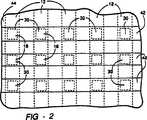
【図2】メモリ素子が1群のX−Yアドレスラインにどのように接続されるかを示す、複数のメモリ素子の考えられるレイアウトの上面図である。
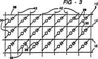
【図3】図1からの複数のメモリ素子の概略図であって、デバイスをそれぞれ互いに電気的に分離するためにダイオードなどの分離素子がどのように1連となってメモリ素子に接続されるかがさらに示された図である。
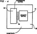
【図4】アドレス/ドライバ/デコーダが動作可能に固定される集積回路チップと電気的に通信状態にある図に示す本発明による集積化されたメモリーマトリックスを持った単結晶半導体基板を示す概略図である。
【発明を実施するための形態】
【0020】
相変化性メモリ材料と不活性誘電材料の混合物を含む複合メモリ材料をここに開示する。本発明によるこの複合メモリ材料は、改良型の電気的メモリ素子の製造に使用できるように高速で低エネルギー入力で広い安定状態の動的範囲内でのスイッチングを可能とするものである。
【0021】
この複合メモリ材料は不揮発性であり、周期的なリフレッシュ信号を必要とすることなく、記憶済み情報の保全性を(選択された誤差範囲内で)維持するものである。記憶済みの情報を変更するために分離して存在する各々のメモリ素子を消去する(指定された開始点に設定する)必要がないように、この複合メモリ材料はまた、直接に上書き可能である。高速で低エネルギーでいかなる異なった抵抗値にもスイッチングできるという機能は、相変化性スイッチング材料の全原子再配置の必要性無くスイッチングが発生するという事実に起因する。
【0022】
すでに述べたように、複合メモリ材料は活性相変化性メモリ材料と不活性誘電材料の混合物である。活性相変化性メモリ材料は複数の構成元素から作成される。相変化性メモリ材料には、Te、Se、Ge、Sb、Bi、Pb、Sn、As、S、Si、P、O又はこれらの混合物もしくは合金からなるグループから選択された1つ以上の元素がある。相変化性メモリ材料は、少なくとも1つのカルコゲン元素を含み、また、少なくとも1つの遷移金属元素を含むのが好ましい。
【0023】
カルコゲン元素はTe、Se及びそれらの混合物もしくは合金からなるグループから選択するのが好ましい。カルコゲン元素はTe及びSeの混合物であればより好ましい。
【0024】
本書で用いる「遷移金属」という用語には、元素(原子番号)21〜30、39〜48、57及び72〜80までが含まれる。遷移金属元素はCr、Fe、Ni、Nb、Pd、Pt及びこれらの混合物もしくは合金からなるグループから選択するのが好ましい。遷移金属がNiであれば最も好ましい。このような複数元素晶系の具体的な例を以下にNi及び/又はSeを持った又は持たないTe:Ge:Sb晶系を参照して述べる。
【0025】
具体的には、本書に述べるテルルは孤立対状態からなる価電子帯を有している。4つの(4)p殻電子がTe中には存在し、Te原子はp殻中のこれら結合電子の内の2つによって化学的に結合されるので、他の2つの外殻電子(孤立対)は結合目的には利用されず、したがって、晶系の原子エネルギーを余り変化させない。この点において、最高度に充填された分子軌道とは、孤立対電子を包含している軌道である。これは重要であるが、その理由は、テルルとゲルマニウムの原子が完全に正規組成された結晶においては、結晶を構成している元の格子中にある程度の内部歪みを印加すると、価電子帯が広がって、既存のフェルミレベルの位置まで上方に移動することがある。しかしながら、TeGe結晶は本質的に「自己補償的」である、すなわち、結晶はTe豊富(約52%がTeで48%がGe)の組成と優先的になることが好ましい。この正規組成結晶は面心立方体であるが、エネルギー量をごくわずかでも付加すれば、そのGe及びSbの空孔の数が増加して、結晶は斜面体格子構造となることがある。TeGe合金内の格子歪みを減少でき、材料のエネルギー状態を下降させ、フェルミレベルを価電子帯に近づけるのは結晶格子構造内のこの空孔の生成である。
【0026】
説明の目的上、短い範囲のローカルオーダーの上に非晶性のローカルオーダーモデルを重ねることが必須でないとしても、原子の動作の記述的説明が完全でないとしても許容されることである。材料の非晶性という本質を考えると、帯域のテール中の欠陥状態の密度が帯域のエッジのところで最大となり、一方、捕獲された電荷担体(chargecarrier)の再結合中心の深さが帯域エッジから遠ざかるほど深くなることに注意されたい。このような深いトラップとテール状態が存在することによって、フェルミレベル位置と帯域エッジ間の中間安定抵抗値に説明がつくかもしれない。理論はともあれ、完全に結晶化した場合、本発明の半導体材料は金属のような導電性を示す縮退型半導体である。
【0027】
さらに、半導体のバルクとメモリ材料内に存在する微結晶の寸法は比較的小さく、約2000Å未満であれば好ましく、約50Åと500Åの間であればさらに好ましく、約200Åと約400Åとの間であればもっとも好ましいと信じられている。さらに、このような微結晶は、異なった抵抗値(導電率)として検出可能な、材料のフェルミレベル位置の急速な形成と、材料が信頼して繰り返し設定することができるこれら検出可能抵抗値間での遷移のための低エネルギー必要量にも貢献する非晶性のスキンで囲まれていると信じられている。
【0028】
本発明による微少結晶材料から製造される2端子又は3端子の半導体デバイスのスイッチング特性の変性は、繰り返し可能で検出可能な抵抗値が実行され得るように制御されることが分かっている。本発明による材料を低エネルギー入力信号によって所望の導電率(フェルミレベル位置によって決まる)に迅速に設定するためには、この材料が、フェルミレベル位置の特徴は実質的に一定の帯域ギャップを持つが電気的導電率は異なるという点にあるが、このフェルミレベルの2つの別々の位置内で安定した(又は長寿命の準安定状態の)存在でありさえずればよい。上記したように、比較的小さい微結晶寸法は検出可能な抵抗値間の迅速な遷移に貢献するとも信じられている。
【0029】
本発明による半導体材料の特徴の1つは、単位体積当たりの微結晶がより小さくそしてより多く形成されるその傾向である。本発明を実現する代表的な材料の最も広い誘電的範囲の微結晶寸法は、約2000Åよりかなり低く、一般的には、先行技術による材料の特徴である約2000Å〜5000Åの範囲未満であることが分かっている。微結晶寸法は微結晶の直径、又は、微結晶が球状でない場合の直径に等しい「特徴的寸法」であると本書では定義されている。
【0030】
本発明の判断基準を満足するTeGeSb材料のクラスの高抵抗状態での組成は一般的に、先行技術による電気的に消去可能なメモリ材料中に存在する濃度に対するTeの濃度がかなり減少するという特徴があることが分かっている。かなり向上した電気的スイッチング性能を持つある1つの組成では、堆積されたままの材料中のTeの平均濃度は70%未満であり、一般的には約60%未満でその範囲は一般的に約23%〜約58%と低いTe濃度であり、約48%〜58%のTe濃度であれば最も好ましい。Geの濃度は材料中で約5%を越え、約8%〜約30の低い範囲であり、残余は一般的に50%未満である。Geの濃度は約8%〜40%の範囲あるのが最も好ましい。この組成中の主要な残余の構成元素はSbである。ここに与えた百分率は、構成元素の原子が合計100%となるような原子百分率である。したがって、この組成の特徴はTeaGebSb100-(a+b)とされる。これらの3元のTe−Ge−Sb合金は電気的特性がさらに良好な追加の相変化性メモリ材料の開発のための開始材料として有用である。
【0031】
相変化性メモリ材料は少なくとも1つのカルコゲンを包含しているのが好ましく、1つ以上の遷移金属を包含できることが好ましい。遷移金属を包含する相変化性材料は、Te−Ge−Sb3元晶系中の相変化性材料の元素変性された形態である。すなわち、元素変性された相変化性材料は、Te−Ge−Sb相変化性合金の変性済み形態を生成する。この元素変性は、Seなどのカルコゲンを追加する化しないかは別として、遷移金属を基本的なTe−Ge−Sb3元晶系中に組み込むことによって達成される。一般的に、元素変性された相変化性材料は2つのカテゴリに分類される。
【0032】
第1のカテゴリは、Te、Ge、Sb及び前記金属を(TeaGebSb100-(a+b))cTM100-c(ここで、添え字は構成元素が合計100%となる原子百分率の値であり、TMは1つ以上の遷移金属であり、a及びbは基本的なTe−Ge−Sb3元晶系に関して上述した値であり、約90%〜約99.99%の間の値である)という比率で含む相変化性メモリ材料である。遷移金属はCr、Fe、Ni、Nb、Pd、Pt並びにこれらの混合物及び合金を含むのが好ましい。
【0033】
この晶系に包括される相変化性メモリ材料の特定の例には次のものが含まれる:(Te56Ge22Sb22)95Ni5、(Te56Ge22Sb22)90Ni10、(Te56Ge22Sb22)95Cr5、(Te56Ge22Sb22)90Cr10、(Te56Ge22Sb22)95Fe5、(Te56Ge22Sb22)90Fe10、(Te56Ge22Sb22)95Pd5、(Te56Ge22Sb22)90Pd10、(Te56Ge22Sb22)95Pt5、(Te56Ge22Sb22)95Pt10、(Te56Ge22Sb22)95Nb5、(Te56Ge22Sb22)90Nb10、(Te56Ge22Sb22)90Ni5Cr5、(Te56Ge22Sb22)90Ni5Fe5、(Te56Ge22Sb22)90Cr5Fe5、(Te56Ge22Sb22)90Pd5Cr5、(Te56Ge22Sb22)90Ni5Pd5、(Te56Ge22Sb22)90Pd5Pt5など。
【0034】
第2のカテゴリはTe、Ge、Sb、Se及び遷移金属を、(TeaGebSb100-(a+b))cTMdSe100-(c+d)(ここで、添え字は構成元素を合計すると100%になる原子百分率値であり、TMは1つ以上の遷移金属であり、a及びbは基本的なTe−Ge−Sb3元晶系に関して上述した値であり、cは約90%〜99.5%の値であり、dは約0.01%〜10%の値である)という比率で含む相変化性メモリ材料である。遷移金属はCr、Fe、Ni、Pd、Pt、Nb並びにこれらの混合物及び合金を含むのが好ましい。この晶系が包括するメモリ材料の特定の例には次のものが含まれる:(Te56Ge22Sb22)90Ni5Se5、(Te56Ge22Sb22)80Ni10Se10、(Te56Ge22Sb22)90Cr5Se5、(Te56Ge22Sb22)80Cr10Se10、(Te56Ge22Sb22)90Fe5Se5、(Te56Ge22Sb22)80Fe10Se10、(Te56Ge22Sb22)90Pd5Se5、(Te56Ge22Sb22)80Pd10Se10、(Te56Ge22Sb22)Pt5Se5、(Te56Ge22Sb22)80Pt10Se10、(Te56Ge22Sb22)90Nb5Se5、(Te56Ge22Sb22)80Nb10Se10、(Te56Ge22Sb22)85Ni5Cr5Se5、(Te56Ge22Sb22)80Ni5Fe5Se10、(Te56Ge22Sb22)85Cr5Fe5、(Te56Ge22Sb22)85Ni5Pd5Se5、(Te56Ge22Sb22)80Ni5Pt5Se10、(Te56Ge22Sb22)85Ni5Nb5Se5、(Te56Ge22Sb22)85Pd5Cr5Se10、(Te56Ge22Sb22)80Pd5Pt5Se10、(Te56Ge22Sb22)85Pd5Nb5Se5、(Te56Ge22Sb22)85Pt5Nb5Se10など。
【0035】
相変化性メモリ材料は、かなり不揮発性の設定抵抗値を有している。しかしながら、相変化性材料の抵抗値がその元の設定値からドリフトする場合、以下に説明する「組成変更(compositional modification)」を用いてこのドリフトを補償してもよい。本書で用いられる、「不揮発性」という用語は、設定抵抗値が永久保存期間にわたって実質的に一定に留まる状態を意味する。もちろん、(以下に説明するフィードバックシステムを含め)ソフトウエアを用いて、選択された誤差範囲を越える「ドリフト」が決して発生しないようにすることができる。メモリ素子の抵抗値のドリフトは、もし妨害されないままであれば、上方のグレースケール記憶を妨害するので、ドリフトを最小化するのが好ましい。
【0036】
「組成変更」は本書では、相変化性メモリ材料の組成を変性して、実質的に安定な抵抗値を生じ、さらに帯域ギャップを広げる元素を付加して材料の固有抵抗を増加させるあらゆる手段を含むものと定義される。組成変更の1例としては、厚さに対するグレーディング済み組成的不均一性を含むものがある。例えば、相変化性メモリ材料の体積は組成の異なる第1のTe−Ge−Sb合金から第2のTe−Ge−Sb合金にまでグレーディングされる。この組成上のグレーディングは、設定抵抗値のドリフトを減少させるようないかなる形態をもとり得る。例えば、組成上のグレーディングは同じ合金晶系の第1と第2の合金に限られる必要はない。また、このグレーディングは3つ以上の合金で遂行することができる。グレーディングは均一で連続であり得ると同時に、また、不均一で不連続でもあり得る。抵抗値のドリフトが減少する結果となる組成上のグレーディングの特定の例には、Ge22Sb22Te56に対する一方の表面から反対側表面でGe14Sb29Te57を均一にそして連続してグレーディングする例がある。
【0037】
組成変更を用いて抵抗値のドリフトを減少させる別の方法は、ある体積の相変化性メモリ材料を積層する方法である。すなわち、ある体積の相変化性メモリ材料を異なった組成を持つ複数の分離した、比較的薄い層で形成できる。例えば、ある体積の相変化性メモリ材料には、各層が別々のTe−Ge−Sb合金で形成された1対以上の層を含むことがある。再度、グレーディング済み組成の場合のように、抵抗値ドリフトをかなり減少させる結果となるいかなる層の組み合わせでも用いることができる。これらの層の厚さは同様であったり異なっていたりする。層をいくつ用いてもよく、同じ合金でできた複数の層が、互いに連続していたり隔たっていたりしてある体積のメモリ材料中に存在してもよい。また、別々の合金をいくつ用いて作成して用いてもよい。組成積層の具体的な例は、Ge14Sb29Te57とGe22Sb22Te56の対が交互に積層されているある体積を持ったメモリ材料である。
【0038】
抵抗値ドリフトを減少させる組成的不均一性のさらに別の形態は、組成グレーディングと組成積層を組み合わせることによって達成される。具体的にいうと、前述の組成グレーディングを上述の組成積層の内のいずれかと組み合わせて、安定したある一定体積のメモリ材料を形成してもよい。この組み合わせを用いる例示体積の相変化性メモリ材料は:(1)Ge22Sb22Te56から成る分離層及びGe14Sb29Te57とGe22Sb22Te56から成るグレーディング済み組成を含むある体積の相変化性メモリ材料と;(2)Ge14Sb29Te57の分離層及びGe14Sb29Te57とGe22Sb22Te56から成るグレーディング済み組成を含むある体積の相変化性メモリ材料と;である。
【0039】
複合メモリ材料は、上述のような活性相変化性メモリ材料及び不活性誘電材料の混合物である。一般的に、誘電材料は、相変化性メモリ材料に対して化学的に不反応性であればどの誘電材料でもよい。融点が相変化性メモリ材料より高い誘電材料が好ましい。
【0040】
特に、誘電材料は、酸化物、窒化物、フッ化物、硫化物、塩化物、カーバイド、窒素酸化物(oxynitride)、窒素炭化物、ほう化物、燐化物並びにこれらの混合物もしくは合金から成るグループから選択された1つ以上の材料であればよい。技術上周知の他の誘電材料を用いてもよい。誘電製材流はまた、有機誘電材料のグループから選択してもよい。これらには、アミド、ポリアミド、イミド、ポリイミド及びパリレン(parylen)などの材料が含まれるがこれらに限定されるわけではない。
【0041】
酸化物には、SiO2などの酸化物、TiO2などの酸化チタニウム、Al2O3などの酸化アルミ、ZrO2などの酸化ジルコニウム、GeO2などの酸化ゲルマニウム、Ta2O5などの酸化タンタルなどがある。他にも考えられる酸化物としては、B2O3、Sb2O3、PbOなどがある。窒化物には、SiN4などの窒化シリコン、AlNなどの窒化アルミ、及びTiN、SiN、ZrN及びBN並びに非化学量論窒化シリコンSiNXなどがある。硫化物には、SiS2などの硫化シリコン、GeS2などの硫化ゲルマニウム及びZnSなどの硫化亜鉛などがある。フッ化物にはMgF2、CaF2、LiF2などがある。
【0042】
さまざまなガラスも使用可能である。例えば、La、Si、O及びNを含むLaSiON材料;Si、Al、O及びNを含むSiAlON材料;イットリウムを含むSiAlON材料;又はNd、Si、O及びNを含むNdSiON;などが用いられる。
【0043】
複合メモリ材料は活性相変化性メモリ材料と不活性誘電材料の異質混合物であるのが好ましい。このような異質混合物の1つの実施形態は、相変化性メモリ材料の層が誘電材料の層と混在している多層構造物のそれである。各層の厚さは約5Å〜約75Åであるのが好ましい。各層の厚さは約10Å〜約50Åであればもっと好ましい。各層の厚さは約20Å〜約30Åであればもっとも好ましい。
【0044】
複合メモリ材料は、RFグロー放電などのプラズマ技法によって効果が増すスパッタリング、蒸着又は化学的気相成長法で製造してもよい。本発明による複合メモリ材料は、無線(RF)スパッタリング又は蒸着で製造するのがもっとも好ましい。それは、一般には相変化性メモリ材料の目標と誘電材料の目標である複数の目標を利用した複数源スパッタリング技法によって形成される。これらの目標が基板の反対側に配置されると、各目標に対して基板を回転させながらスパッタリングが実行される。相変化性材料と誘電材料の双方を含んでいる目標を用いてもよい。また、基板を加熱して、表面移動による結晶成長及び結晶凝集に影響を与えることによって形成された複合材料内の相変化性材料の形態を制御してもよい。
【0045】
複合メモリ材料中の誘電材料の体積百分率は制御可能である。誘電材料の体積百分率は約10%〜約90%の間であるのが好ましい。誘電材料の体積百分率は約20%〜約80%であればより好ましい。誘電材料の体積百分率は約40%〜約60%であればもっとも好ましい。
【0046】
複合メモリ材料はまた、スピンコーティングによっても製造される。相変化性メモリ材料はポリアミドのような有機重合体などの誘電体と混合してもよい。その結果得られた混合物は次に、シリコン基板上でスピンコーティングされて、所望の特性を持った複合メモリ材料を形成する。
【0047】
上記で開示した複合メモリ材料を含む単一セルメモリ素子をまたここに開示する。このメモリ素子はまた、複合メモリ材料に電気入力信号を出力するための離間配置された1対のコンタクトをさらに含んでいる。図1に、単結晶シリコン半導体ウエハ10上に形成されたメモリ素子の実施形態の断面図を示す。このメモリ素子は複合メモリ材料、離間配置された第1のコンタクト6及び離間配置された第2のコンタクトを含んでいる。
【0048】
第1のコンタクト6及び第2のコンタクト8はそれぞれが2つの薄膜層から成る。複合メモリ材料36に隣接して堆積された薄膜層38と34は、異物が複合メモリ材料36中に拡散して電気的マイグレーションする優れた拡散バリヤ特性を有する。
【0049】
隣接した薄膜層38と34は非晶性炭素などの炭素材料から成っていてもよい。あるいは、隣接薄膜層38と34を、Ti、V、Cr、Zr、Nb、M、Hf、Ta、Wから成るグループから選択された1つの元素とB、C、N、Al、Si、P、Sから成るグループからから選択された1つ以上の元素を含む化合物から形成してもよい。隣接薄膜層38と34は、Ti並びに、C、N、Al、Si並びにこれらの混合物又は合金から成るグループから選択された1つ以上の元素を含む化合物から形成するのが好ましい。ある実施形態では、隣接薄膜層は、原子百分率で、約10%〜60%のチタニウム、5%〜50%の炭素及び10%〜60%の窒素から成っている。その上、炭化チタニウムもまた、最大で40%の水素を含んでいる。
【0050】
別の実施形態では、隣接薄膜層38と34は、シリコン窒化チタニウムから成っている。この実施形態では、隣接薄膜層は、原子百分率で約10%〜60%のチタニウム、5%〜50%のシリコン及び10%〜60%の窒素という組成を有する化合物から成るのが好ましい。その上、シリコン窒化チタニウムもまた最大で40%の水素を含んでいる。
【0051】
第3の実施形態では、隣接薄膜層38と34は、アルミ窒化チタニウムから成っている。この実施形態では、隣接薄膜層は、原子百分率で約10%〜60%のチタニウム、5%〜50%のアルミニウム及び10%〜60%の窒素という組成を有する化合物から成るのが好ましい。その上、アルミニウム窒化チタニウムもまた最大で40%の水素を含んでいる。
【0052】
炭素窒化チタニウム、シリコン窒化チタニウム及びアルミ窒化チタニウムは優れたバリヤ特性を有し、これによって異物が複合メモリ材料中に拡散したり電気的マイグレーションするのを防いでいる。さらに、炭素窒化チタニウム、シリコン窒化チタニウム及びアルミニウム窒化チタニウムは、蒸着を含む物理的気相成長法、イオン打ち込み法及びDCとRFスパッタリング堆積法、化学的気相成長法並びにプラズマ支援型化学的気相成長法などの方法によって堆積してもよい。その方法が正しいかは多くの要因によるが、その要因の1つは、目標となる材料の組成に起因する堆積温度の制約である。
【0053】
1対の離間配置されたコンタクト6と8は、複合メモリ材料36から遠隔に堆積された追加の薄膜層相32と40から成るのが好ましい。これらの遠隔薄膜層のおのおのが、Ti、W及びMoから成るグループから選択された1つ以上の元素から成っている。ある実施形態では、各遠隔薄膜層はTiとWから成っている。遠隔薄膜層は、原子百分率で5%〜30%のチタニウムと70%〜95%のタングステンの化合物から成っているのが好ましい。Ti−W合金層32と40は、DCスパッタリング堆積プロセスで堆積するのが好ましい。これらは約100Å〜2000Åに厚さに堆積するのが好ましい。これらは約100Å〜4000Åに厚さに堆積するのが好ましい。Ti−W合金層32と40は優れたオーム接触特性を有している。そのうえ、これらは、複合メモリ材料36中への異物の電気的マイグレーションと拡散の双方を防ぐに必要なバリヤ特性を有している。
【0054】
複合メモリ材料36の層は、約200Å〜5000Åの厚さに堆積するのが好ましく、約250Å〜2500Åの堆積厚さがより好ましく、約250Å〜500Åの厚さに堆積するのがもっとも好ましい。
【0055】
図1に示すメモリ素子は複数ステッププロセスで製造される。層32、34及び46は最初に堆積され、次に絶縁層46がエッチングされて、複合メモリ材料36と層34の間にコンタクトのための領域ができるようにする。残っている層36、38及び40が堆積され、層32、34、36、46、38、及び40の全堆積層が選択された寸法にエッチングされる。全体構造物の上に絶縁材料39の層が堆積される。絶縁材料の例としてはSiO2、Si3N4及び酸素硫化テルル(例えばTeOS)がある。絶縁材料39の層はエッチングされ、アルミニウム層が堆積されて、導体12に向けて直角に伸長する第2の電極グリッド構造物42を形成して、個別のメモリ素子に対するX−Yグリッド接続を完成させる。この完成された集積構造体の上には、性能を劣化させたり縮退させたりしかねない湿気や他の外部要因からこの構造物を密封するSi3N4又はポリアミドなどの可塑性材料などの適当なカプセル封入材から成る頂部カプセル封入層が重なっている。Si3N4カプセル封入材は、例えば低温プラズマ堆積プロセスを用いて堆積することができる。このポリアミド材料は堆積後に周知の技法に従ってスピンコーティングしてベーキングしてカプセル封入層を形成する。
【0056】
本書で用いる「孔径(pore diameter)」という用語は、複合メモリ材料36間での最小のコンタクト領域並びに電気的コンタクト6及び8の平均の断面のことである。孔径はリソグラフィの分解能の限界が許す限り小さくできる。孔径はデバイスの性能に関連がある。孔径を減少させるとデバイスの体積が減少し、これによって電気的スイッチングに要する電流とエネルギーの必要量が低下する。これによってデバイスの速度と感度が増し、検出可能な抵抗値変化を始動するに必要なスイッチング時間と電気的エネルギーが減少する。
【0057】
メモリ素子に関する以前の実施形態では、孔径は、材料が高低の抵抗状態間をいずれの方向にもスイッチングした際に実際に変化する抵抗を持つメモリ材料の断面に実質的に適合するように選択するのが好ましい。メモリ材料のこのセクションは「線条部分(フィラメント部分、filamentary portion)」と呼ばれる。孔径は線条部分の直径に等しいのが理想である。
【0058】
孔径をリソグラフィが許容する値を越えて減少させる手段として、メモリ素子の以前の実施形態では、離間配置されたコンタクトの内の少なくとも1つとメモリ材料の体積の間に「線条制限手段(フィラメント制限手段、filament confining means)」が用いられていた。線条制限手段は一般的には、電気的コンタクトとメモリ材料体積間を電流が通過する少なくとも1つの低抵抗通路を持つ高抵抗性材料から成る薄膜層である。線条制限手段は、離間配置されているコンタクトに非常に低い電流が入力されると、線条部分内に高電流密度をもたらした。
【0059】
線条制限手段は、メモリデバイスの「電気的形成プロセス」において一つの役割を演ずるのである。この電気的形成プロセスは、メモリ素子がその最初の非常に高い「バージン」抵抗値から低い抵抗値に切り替わるまで、より高電流の電気パルスを製造されたばかりのメモリ素子に印加する、というものである。ひとたびこれが行われれば、メモリ素子は「形成された」と言われる。これで、より低いプログラミング電流によって電気的サイクリングを行う準備ができたことになる。
【0060】
この形成プロセスによって線条制限手段が「ブレークダウン」される。この形成プロセスの際の一又は複数のより高い電流パルス印加において、制限層内でもっとも電気的に弱い「ブレークダウン」領域が物理的に変化して、層の他の部分より遥かに導電性が高くなる。その後に続くあらゆるメモリサイクリングパルス(すなわちセットパルスとリセットパルス)による電流が通過するのはこの領域である。非常に低い電流がメモリ素子に印加されると、すべての電流が線条部分を通過して流れる。すなわち、その寸法が極端に小さいため、メモリ材料のこの領域内での電流密度は非常に高くなる。
【0061】
メモリ素子の以前の実施の形態においては、電気的サイクリングに必要なプログラミング電流は、孔径をリソグラフィによって小さくするか、或いは線条制限手段の導入によるかのいずれかの方法によって低減されていた。これに対して、本発明による複合材料を含むメモリ素子では、プログラミング電流は、不活性誘電材料を導入することによって相変化性材料の体積を制限することによって、所望の電流低減を達成するのである。
【0062】
この新規複合材料の選択した体積部分を誘電材料で占有させることによって、活性な相変化性メモリ材料が占有する体積部分を減少させることができる。この活性な相変化性メモリ材料の体積比率の減少によって、メモリ素子をプログラミングするのに必要とされる電流値が低減されるのである。
【0063】
誘電材料の体積比率を制御することができるので、薄膜メモリへの応用において、電気伝導性材料の体積は、フォトリソグラフィで画定されるコンタクト領域の寸法に拘束されることなく、制御可能なのである。これによって、与えられたフォトリソグラフィ技術のスケールにおいて、必要とされるプログラミング電流を、メモリドライバから供給可能な電流にかなった電流値にまで低減することができるのである。
【0064】
従って、本発明の複合材料は、上述の線条制限手段と同様の機能を果たすのである。線条制限手段を併用して本発明の複合材料を用いれば、電気的形成プロセス及びスイッチングの際に、メモリ材料内において線条部分の断面積が決められるのである。すなわち、本発明による複合材料を用いれば、さらに材料層を追加する必要なく、微細孔を形成するリソグラフィ技術の限界が克服されるのである。
【0065】
また、単一セルメモリ素子を規定するある体積を持つメモリ材料であり、このメモリ材料が、単一セルに複数ビット記憶機能を備えるために選択済み電気入力信号に反応しての材料の以前の抵抗値とは無関係に、特定の開始抵抗値や消去済み抵抗値に設定する必要なく、後出の動的範囲内で複数の抵抗値の内の1つに直接的に設定される機能を持った電気抵抗値の大きな動的範囲を得るための手段を構成しているある体積のメモリ材料を含む、電気的に動作する、直接に上書き可能で、マルチビットの単一セルメモリ素子をここに開示する。
【0066】
この電気的に動作する、直接上書き可能で、マルチビットの、単一セルメモリ素子はさらに、動的範囲内の選択済み抵抗値にメモリ材料を設定するために電気入力信号を供給するための1対の離間配置されたコンタクトをさらに含んでいる。少なくとも一方の離間配置されたコンタクトは第1と第2のコンタクト最良の混合物である。第1のコンタクト材料は炭素を含み、第2のコンタクト材料は少なくとも1つの遷移金属元素を含んでいる。本書で用いる「遷移金属」という用語は、元素(原子番号)21〜30、39〜48、57及び72〜80の元素を含む。第2のコンタクト材料は、Ti、V、Cr、Zr、Nb、Mo、Hf、Ta、W並びにこれらの混合物もしくは合金からなるグループから選択された1つ以上の元素を含むのが好ましい。第2のコンタクト材料はTi及びWを含むのがより好ましい。コンタクトは共スパッタリングプロセスで製造することができる。
【0067】
複数メモリ素子の考えられる構成の上面図を図2に示す。図示するように、デバイスはメモリ素子のX−Yマトリックスを形成する。水平方向片2は個別の素子をアドレス指定するためのX−Y電極グリッドのX集合を表している。縦方向片42はアドレス指定ラインのY集合を表している。
【0068】
本発明による電気的に消去可能な記憶装置の他の回路構成はもちろん考えられるし実現可能である。1つの特に有用な構成は、複数の平面を成すメモリ素子又は制御素子並びにその個別の絶縁デバイスが互いに積層されている3次元の、複数レベル配列である。各平面を成すメモリ素子はメモリ素子の複数の行と列として配置され、これによってX−Yアドレス指定を可能としている。この平面積層によって、記憶蓄積密度が増すほかにも、相互接続のさらなるX次元が可能となる。この配置は、真にインテリジェントなコンピュータの神経網をシミュレートするには特に有用である。
【0069】
各メモリ素子はある種のタイプの絶縁素子を用いて電気的に互いに絶縁される。図3のメモリデバイスレイアウトに概略図に、ダイオードを用い実行される電気的絶縁方法が示されている。この回路は絶縁ダイオード26と直列に相互接続されたメモリ素子30を持ったX−Yグリッドを含む。アドレスライン12と42は、当業者には周知の方法で外部アドレス指定回路に接続されている。この絶縁素子の目的は、分離した各メモリ素子を、マトリックス内の隣接した又は遠隔のメモリ素子に記憶されている情報に干渉することなく読み出しと書き込みを可能とすることにある。
【0070】
図4に、本発明によるメモリーマトリックス(MEMORY MATRIX)51が形成された単結晶半導体基板(SUBSTRATE)50の1部分を示す。また、この基板50上には、集積回路線53によってメモリーマトリックス51に適切に接続されているアドレス指定マトリックス(ADDRESSING MATRIX)52が形成されている。アドレス指定マトリックス52は、メモリーマトリックス51に印加される設定パルス及び読み取りパルスを画定して制御する信号発生手段を含んでいる。もちろん、アドレス指定マトリックス52はソリッドステートメモリーマトリックス51と同時に集積して形成してもよい。
【0071】
実験の結果、カルコゲン組成、熱処理(堆積後アニール)、信号パルス持続時間、組成中の酸素などの不純物、結晶寸法及び信号パルス波形形状などの要素は抵抗の動的範囲の大きさ、この動的範囲の絶対終点抵抗及びデバイスをこれらの抵抗値に設定するに必要とされる電圧に影響を与えることが分かっている。例えば、カルコゲン化物薄膜(例えば約4000Å)が比較的厚いため、設定電圧必要値が高く(したがってメモリ材料体積内の電流密度が高く)なるが、一方、カルコゲン層が比較的薄い(例えば約250Å)と、設定電圧(及び電流密度)の必要値が低くなる。もちろん。結晶寸法及び、従ってバルク原子の数に対する表面原子の数の比の潜在的重要性はすでに論じた。
【0072】
抵抗値の動的範囲によってまた、広いグレースケール及び複数レベルのアナログ記憶蓄積が可能となる。複数レベル記憶蓄積は、広い動的範囲を複数のサブ範囲又はレベルに分割することによって遂行される。連続して抵抗値をプログラミングできることによって、複数ビットのバイナリ情報を1つのメモリーセルに記憶できる。この複数レベル記憶は、複数ビットのバイナリ情報を擬似アナログ形態に模擬して、このアナログ情報を単一メモリーセルに記憶することによって遂行される。したがって、抵抗値の動的範囲を2n個のアナログレベルに分割することによって、各メモリーセルはnビットのバイナリ情報を記憶する能力が与えられる。
【0073】
本書に開示する所有権保護された材料とデバイス構成を用いることによって、SRAMに近い読み出し・書き込み速度を持ち;EEPROMの不揮発性でランダムアクセス再プログラミング機能を持ち;メガバイト記憶容量当たりの価格が他のいかなる半導体メモリー未満である;電気的に消去可能で、直接的に上書き可能なメモリ素子が開発された。
【0074】
ここに記載する開示は本発明を全部そして完全に開示する目的で述べた詳細な実施形態という形で提示されたものであり、このような詳細は、添付クレームに記載し定義される本発明の真の範囲を制限するものであると解釈すべきでないことを理解されたい。【Technical field】
[0001]
The present invention generally relates to electrically operating memory materials. More specifically, the present invention relates to a composite memory material comprised of a mixture of an active phase change memory material and an inert dielectric material.
[Background]
[0002]
Ovonic's EEPROM is a new, proprietary, high performance, non-volatile thin film electronic memory device. This means that data can be stored in a non-volatile manner, the potential for high bit density, and as a result, low cost due to a simple two-terminal device configuration with a small footprint, long programming cycle life, It has the advantages of low programming energy and high speed. Ovonic EEPROMs can store information in both analog and digital form. Digital storage can be either binary (1 bit per memory cell) or multi-state (multiple bits per cell). Only a minor modification is required to switch between the two digital modes. For purposes of describing the present invention, the terms “memory element” and “control element” are used interchangeably.
[0003]
Early electrical phase change memory
The general concept of utilizing electrically writable and erasable phase change materials (ie, materials that are electrically switched between a generally amorphous state and a generally crystalline state) for electronic memory applications is Well known in the art, for example, U.S. Pat. No. 3,271,591 to Ovsinsky, issued September 6, 1966, and Obsinsky, issued September 22, 1970. U.S. Pat. No. 3,530,441, both of which are incorporated herein by reference (hereinafter referred to as the "Ovshinsky patent").
[0004]
As disclosed in the Ovshinsky patent, such materials can be used between two structural states, a generally amorphous local order and a generally crystalline local order, or between a completely amorphous state and a completely crystalline state. It may be electrically switchable between distinct local order states that can be detected across the entire spectrum in between. That is, the electrical switching of such materials does not have to occur between a completely amorphous state and a completely crystalline state, but rather reflects changes in local order in incremental steps. Thus, the Obsinsky patent states that it provides a “grayscale” represented by a number of local order states that encompass the spectrum between the completely amorphous and fully crystalline states. Early materials described by the Obshinsky patent also address storage and retrieval of single-bit encoded binary information, if necessary, by switching between a generally amorphous and a generally crystalline structure state. You can also.
[0005]
The electrically erasable phase change memory and subsequent electrical solid state memory described in the Obshinsky patent are tape, floppy disk, magnetic hard disk drive, optical hard disk drive, solid state disk flash, DRAM, SRAM, and socket flash. It has many limitations that preclude its widespread use in direct and general replacement for current computer applications such as memory. Specifically, the most important of these limitations are listed below: (i) relatively slow (to current standards) electrical switching speeds, particularly large local order directions (increasing crystallinity) (Ii) a relatively high input energy requirement needed to trigger a detectable change in local order; and (iii) a relatively high cost per megabyte of stored information (Especially noticeable compared to current hard disk media).
[0006]
The most important of these limitations is that the energy input required to obtain a detectable change in the chemical and / or electronic binding configuration of the chalcogenide material to trigger a local order detectable change is relatively high. It is expensive. Also important was the switching time of the electrical memory material described in the Obshinsky patent. These materials generally have a set time (time required to switch state from amorphous to crystalline) in the range of a few milliseconds; and a reset time of about 1 microsecond (from material to crystalline Time required to switch the state to crystalline). The electrical energy required to switch between these materials was typically measured in the range of about 1 microjoule.
[0007]
This amount of energy is sent to each memory element in the matrix solid state matrix of memory cells. Such high energy levels translate into high current carrying requirements for address lines and cell isolation / address devices associated with each independent memory element. Given these energy requirements, those skilled in the art will want to choose memory cell isolation for micron-order lithography, and therefore for very large single diodes or transistors that make memory devices as dense as possible. Limited. Thus, a low bit density matrix array made from this material has a high cost per megabyte of stored information.
[0008]
By effectively reducing the price and performance differences between permanent storage non-volatile mass memory and high-speed volatile system memory, the memory device according to the present invention is a novel, non-hierarchical “general purpose storage device” Has the ability to Virtually all of the memory in the system can be inexpensive, permanently stored and fast. Compared to the first Obshinsky type phase change electrical memory, the memory materials described herein have a programming time of over six orders of magnitude (less than 30 nanoseconds) and extremely low programming energy (0.1 Long-term stability and cycleability (over 10 trillion cycles). In addition, according to the experimental results, an increase in switching speed and cycle life was recognized due to a decrease in the size of the element.
[0009]
In general, the development and optimization of a class of chalcogenide memory materials has not progressed at the same speed as other types of solid-state electrical memories that currently have much faster switching times and much lower set and reset energies. These other forms of memory typically use one or two solid state microelectronic circuit elements (3 or 4 transistors per bit) for each memory bit in some memory applications. The main “non-volatile” memory element in the solid state memory field such as EEPROM is generally a floating gate that has limited reprogrammability and holds the charge at the gate of the field effect transistor to store each memory bit Type field effect transistor devices. Since this charge leaks over time, it is truly non-volatile, as in prior art phase change media where information is stored through changes in the actual atomic configuration or electronic structure of the chalcogenide material from which the device is fabricated. It's not gender. These other forms of memory are currently received in the market.
[0010]
In contrast to other “flash” devices such as DRAM and SRAM, volatile memory, and floating gate structures, no field effect transistor device is required for the electrical memory device according to the present invention. In fact, an electrically erasable and directly overwritable memory device according to the present invention is the most manufacturable electrical device, including only two electrical contacts to a monolithic body of thin film chalcogenide material and a semiconductor diode for isolation. Typical memory device. As a result, only a very small “realestate” is needed to store one bit of information, thereby providing a memory chip that is inherently dense. Furthermore, the information density is further increased by adopting a method of storing a plurality of bits in each discrete memory cell.
[0011]
In order to handle the flash EEPROM market and be considered as a general purpose memory, the memory device must be truly non-volatile. This is even more important when the memory element needs to have a multi-bit storage function. If the set resistance value is lost or found to drift considerably over time, the information stored therein is destroyed and the user does not trust the permanent storage function of the memory.
[0012]
In addition to set resistor stability, another important factor required for general purpose memory is low switching current. This is very important if the EEPROM is stored permanently on a large scale. When used in this manner, the EEPROM replaces the mechanical hard disk (eg, magnetic hard drive or optical hard drive) of current computer systems. One of the main reasons for using EEPROM “hard drives” instead of conventional mechanical hard drives is the relatively high power consumption inherent in mechanical devices. For laptop computers, this is particularly important because mechanical hard disk drives are the most power consuming components. Therefore, it is particularly advantageous to reduce this power and increase the computer usable time each time the power battery is charged once. However, using an EEPROM instead of a mechanical hard drive increases the switching energy requirement (and therefore the power requirement), so the power savings are insignificant or at best not significant. Therefore, the switching energy of the EEPROM to be considered as a general-purpose memory needs to be low.
[0013]
Yet another requirement of an EEPROM general purpose memory is that the stored information has a high thermal stability. Today's computers, especially personal computers, are constantly exposed to high temperatures. This high temperature can be caused by heat from the power source and other heat generating internal components. This high temperature can also be caused by using the computer in a hot climate or storing the computer in an environment that is indirectly or directly heated at a temperature higher than room temperature. Whatever the cause of the high temperature, current computer devices, particularly “hard” or permanently stored memories, must be thermally stable at fairly high temperatures. Without this thermal stability, data is lost and the aforementioned reliability is lost.
[0014]
Yet another requirement for EEPROM general purpose memory is a long write / erase cycle life. In the case of EEPROM, as with permanent storage memory, cycle life plays an important role in consumer confidence and acceptance. If the cycle life of a memory device is too short, consumers are reluctant to use the device for fear of losing valuable data. This requirement of long cycle life becomes even more important when EEPROM is used in place of computer main storage or display storage, ie, in place of DRAM, SRAM or VRAM. The main storage device and the display storage device are data storage areas that are most frequently written / erased in a computer. Each time a new computer program is loaded, a portion of the computer's main memory is erased and rewritten. During execution of a computer program, a portion of the computer's main memory is always cycled. If the EEPROM used in place of the computer's main storage and display storage does not have a relatively long write / erase cycle life, these memories will most likely need to be replaced.
SUMMARY OF THE INVENTION
[0015]
It is an object of the present invention to provide a solid state memory material with reduced switching current requirements and increased thermal stability of stored data. Another object of the present invention is to provide a memory device comprising the aforementioned memory material.
[0016]
These and other objects of the present invention are achieved by a composite memory material consisting of a mixture of an active phase change memory material and an inactive dielectric material. The phase change memory material includes one or more elements selected from the group consisting of Te, Se, Ge, Sb, Bi, Pb, Sn, As, S, Si, P, O and mixtures or alloys thereof. Is included.
[0017]
These and other objects are also achieved by a single cell memory device consisting of: That is, a memory material of a fixed volume that defines a memory element, which is a memory material composed of a mixture of an active phase change material and an inactive dielectric material, and reads information stored in the memory element A single cell memory device comprising a pair of spaced contacts that serve as terminals for writing to the memory device.
[0018]
These and other objects are also achieved by an electrically operated, directly overwritable, multi-bit single cell memory device consisting of: That is,
(A) a constant volume of memory material defining a single cell memory device,
The memory material provides multi-bit recording capability for the single cell;
Does not require setting to a specific starting or erasing resistance value, and directly sets one of a plurality of resistance values within the dynamic range in response to a selected electrical input signal, regardless of the previous resistance value of the material Can be
A memory material comprising means having a dynamic range with a large electrical resistance value; and (b) supplying the electrical input signal to set the memory material to a selected resistance value within the dynamic range. A pair of contacts arranged at intervals,
At least one of the spaced contacts is a mixture of a first contact material and a second contact material, the first contact material comprising carbon, and the second contact material is at least one transition. It is a memory element comprising a pair of contacts which are arranged at an interval including a metal element.
The second contact material preferably contains one or more elements selected from the group consisting of Ti, V, Cr, Zr, Nb, Mo, Hf, Ta, W or mixtures or alloys thereof. It is particularly preferred that the second contact material contains Ti and W.
[Brief description of the drawings]
[0019]
FIG. 1 is a cross-sectional view of a single memory device showing a composite memory material and a pair of contacts.
FIG. 2 is a top view of a possible layout of a plurality of memory elements, showing how the memory elements are connected to a group of XY address lines.
FIG. 3 is a schematic diagram of a plurality of memory elements from FIG. 1, in which isolation elements such as diodes are connected in series to the memory elements to electrically isolate the devices from each other, respectively. FIG.
FIG. 4 is a schematic diagram illustrating a single crystal semiconductor substrate having an integrated memory matrix according to the present invention shown in the figure in electrical communication with an integrated circuit chip to which an address / driver / decoder is operatively fixed. It is.
BEST MODE FOR CARRYING OUT THE INVENTION
[0020]
Disclosed herein is a composite memory material comprising a mixture of a phase change memory material and an inert dielectric material. This composite memory material according to the present invention enables switching within a wide steady state dynamic range with high speed, low energy input, so that it can be used in the manufacture of improved electrical memory devices.
[0021]
This composite memory material is non-volatile and maintains the integrity of the stored information (within a selected error range) without the need for a periodic refresh signal. This composite memory material can also be directly overwritten so that there is no need to erase (set to a specified starting point) each memory element that exists in isolation to alter stored information. . The ability to switch to any different resistance value at high speed and low energy is due to the fact that switching occurs without the need for total atom rearrangement of the phase change switching material.
[0022]
As already mentioned, the composite memory material is a mixture of an active phase change memory material and an inert dielectric material. The active phase change memory material is made from a plurality of constituent elements. The phase change memory material includes one or more elements selected from the group consisting of Te, Se, Ge, Sb, Bi, Pb, Sn, As, S, Si, P, O or mixtures or alloys thereof. is there. The phase change memory material includes at least one chalcogen element and preferably includes at least one transition metal element.
[0023]
The chalcogen element is preferably selected from the group consisting of Te, Se and mixtures or alloys thereof. The chalcogen element is more preferably a mixture of Te and Se.
[0024]
As used herein, the term “transition metal” includes elements (atomic numbers) 21-30, 39-48, 57 and 72-80. The transition metal element is preferably selected from the group consisting of Cr, Fe, Ni, Nb, Pd, Pt and mixtures or alloys thereof. Most preferably, the transition metal is Ni. Specific examples of such a multi-element crystal system will be described below with reference to a Te: Ge: Sb crystal system with or without Ni and / or Se.
[0025]
Specifically, tellurium described in this document has a valence band composed of an isolated pair state. Since four (4) p-shell electrons are present in Te and the Te atom is chemically bonded by two of these bonded electrons in the p-shell, the other two outer electrons (lone pairs) ) Is not used for bonding purposes and therefore does not change the crystal atomic energy much. In this regard, the highest packed molecular orbital is an orbital that contains lone pair electrons. This is important because, in crystals with a perfectly regular composition of tellurium and germanium atoms, when a certain amount of internal strain is applied to the original lattice constituting the crystal, the valence band is increased. It can spread and move up to the existing Fermi level position. However, it is preferred that TeGe crystals are essentially “self-compensating”, that is, the crystals are preferential with a Te-rich composition (about 52% Te and 48% Ge). The regular composition crystal is a face-centered cube, but if a very small amount of energy is added, the number of Ge and Sb vacancies increases, and the crystal may have a sloped lattice structure. It is the creation of these vacancies in the crystal lattice structure that can reduce the lattice strain in the TeGe alloy, lower the energy state of the material, and bring the Fermi level closer to the valence band.
[0026]
For the purposes of explanation, it is acceptable even if it is not essential to overlay an amorphous local order model on a short range of local orders, but a descriptive explanation of the behavior of the atoms is not complete. Given the essence of the amorphous nature of the material, the density of defect states in the tail of the band is maximized at the edge of the band, while the recombination center depth of the trapped charge carrier is from the band edge. Note that it gets deeper as you move away. The presence of such deep trap and tail states may account for the intermediate stable resistance value between the Fermi level position and the band edge. Whatever the theory, when fully crystallized, the semiconductor material of the present invention is a degenerate semiconductor that exhibits electrical conductivity such as metal.
[0027]
Further, the size of the microcrystals present in the semiconductor bulk and memory material is relatively small, preferably less than about 2000 mm, more preferably between about 50 mm and 500 mm, and between about 200 mm and about 400 mm. It is believed that it would be most desirable. In addition, such microcrystals can be detected as different resistance values (conductivity), between the rapid formation of the Fermi level position of the material and the detectable resistance value that the material can be reliably set repeatedly. It is believed to be surrounded by an amorphous skin that also contributes to the low energy requirements for the transition at.
[0028]
It has been found that the modification of the switching characteristics of a two-terminal or three-terminal semiconductor device manufactured from a microcrystalline material according to the invention is controlled such that a repeatable and detectable resistance value can be implemented. In order to quickly set the material according to the invention to the desired conductivity (determined by the Fermi level position) with a low energy input signal, the material has a substantially constant band gap with the Fermi level position characteristic. Although the electrical conductivity is different, it only needs to be stable (or in a long-lived metastable state) within two separate locations of this Fermi level. As noted above, relatively small crystallite sizes are also believed to contribute to a rapid transition between detectable resistance values.
[0029]
One of the features of the semiconductor material according to the invention is its tendency to form smaller and more microcrystals per unit volume. The widest dielectric range crystallite size of a representative material embodying the present invention is much lower than about 2000 mm, and generally less than the range of about 2000 mm to 5000 mm, which is characteristic of prior art materials. I know. The crystallite size is defined herein to be the “characteristic dimension” equal to the diameter of the crystallite, or the diameter when the crystallite is not spherical.
[0030]
The composition in the high resistance state of a class of TeGeSb materials that meet the criteria of the present invention is generally characterized by a significant decrease in the concentration of Te relative to the concentration present in electrically erasable memory materials according to prior art I know that there is. In one composition with significantly improved electrical switching performance, the average concentration of Te in the as-deposited material is less than 70%, typically less than about 60%, and the range is generally about A Te concentration as low as 23% to about 58%, and a Te concentration of about 48% to 58% is most preferred. The concentration of Ge is greater than about 5% in the material, ranging from about 8% to about 30 and the remainder is generally less than 50%. Most preferably, the concentration of Ge is in the range of about 8% to 40%. The main remaining constituent element in this composition is Sb. The percentage given here is an atomic percentage in which the atoms of the constituent elements are 100% in total. Therefore, the characteristics of this composition are TeaGebSb100- (a + b)It is said. These ternary Te-Ge-Sb alloys are useful as starting materials for the development of additional phase change memory materials with better electrical properties.
[0031]
The phase change memory material preferably includes at least one chalcogen and preferably can include one or more transition metals. The phase change material including the transition metal is an elementally modified form of the phase change material in the Te-Ge-Sb ternary system. That is, the elementally modified phase change material produces a modified form of the Te—Ge—Sb phase change alloy. This elemental modification is achieved by incorporating a transition metal into the basic Te—Ge—Sb ternary system, with or without the addition of chalcogens such as Se. In general, elementally modified phase change materials fall into two categories.
[0032]
The first category is Te, Ge, Sb and the metal (TeaGebSb100- (a + b))cTM100-c(Here, the subscript is an atomic percentage value in which the constituent elements are 100% in total, TM is one or more transition metals, and a and b are basic values.Te-Ge-SbA phase change memory material comprising a ratio of about 90% to about 99.99%) described above with respect to a ternary crystal system. Transition metals preferably include Cr, Fe, Ni, Nb, Pd, Pt, and mixtures and alloys thereof.
[0033]
Specific examples of phase change memory materials encompassed by this crystal system include: (Te56Getwenty twoSbtwenty two)95NiFive, (Te56Getwenty twoSbtwenty two)90NiTen, (Te56Getwenty twoSbtwenty two)95CrFive, (Te56Getwenty twoSbtwenty two)90CrTen, (Te56Getwenty twoSbtwenty two)95FeFive, (Te56Getwenty twoSbtwenty two)90FeTen, (Te56Getwenty twoSbtwenty two)95PdFive, (Te56Getwenty twoSbtwenty two)90PdTen, (Te56Getwenty twoSbtwenty two)95PtFive, (Te56Getwenty twoSbtwenty two)95PtTen, (Te56Getwenty twoSbtwenty two)95NbFive, (Te56Getwenty twoSbtwenty two)90NbTen, (Te56Getwenty twoSbtwenty two)90NiFiveCrFive, (Te56Getwenty twoSbtwenty two)90NiFiveFeFive, (Te56Getwenty twoSbtwenty two)90CrFiveFeFive, (Te56Getwenty twoSbtwenty two)90PdFiveCrFive, (Te56Getwenty twoSbtwenty two)90NiFivePdFive, (Te56Getwenty twoSbtwenty two)90PdFivePtFiveSuch.
[0034]
The second category is Te, Ge, Sb, Se and transition metals, (TeaGebSb100- (a + b))cTMdSe100- (c + d)(Where the subscripts are atomic percentage values that add up to 100% of the constituent elements, TM is one or more transition metals, and a and b are described above for the basic Te-Ge-Sb ternary system. And c is a value of about 90% to 99.5%, and d is a value of about 0.01% to 10%). Transition metals preferably include Cr, Fe, Ni, Pd, Pt, Nb and mixtures and alloys thereof. Specific examples of memory materials encompassed by this crystal system include: (Te56Getwenty twoSbtwenty two)90NiFiveSeFive, (Te56Getwenty twoSbtwenty two)80NiTenSeTen, (Te56Getwenty twoSbtwenty two)90CrFiveSeFive, (Te56Getwenty twoSbtwenty two)80CrTenSeTen, (Te56Getwenty twoSbtwenty two)90FeFiveSeFive, (Te56Getwenty twoSbtwenty two)80FeTenSeTen, (Te56Getwenty twoSbtwenty two)90PdFiveSeFive, (Te56Getwenty twoSbtwenty two)80PdTenSeTen, (Te56Getwenty twoSbtwenty two) PtFiveSeFive, (Te56Getwenty twoSbtwenty two)80PtTenSeTen, (Te56Getwenty twoSbtwenty two)90NbFiveSeFive, (Te56Getwenty twoSbtwenty two)80NbTenSeTen, (Te56Getwenty twoSbtwenty two)85NiFiveCrFiveSeFive, (Te56Getwenty twoSbtwenty two)80NiFiveFeFiveSeTen, (Te56Getwenty twoSbtwenty two)85CrFiveFeFive, (Te56Getwenty twoSbtwenty two)85NiFivePdFiveSeFive, (Te56Getwenty twoSbtwenty two)80NiFivePtFiveSeTen, (Te56Getwenty twoSbtwenty two)85NiFiveNbFiveSeFive, (Te56Getwenty twoSbtwenty two)85PdFiveCrFiveSeTen, (Te56Getwenty twoSbtwenty two)80PdFivePtFiveSeTen, (Te56Getwenty twoSbtwenty two)85PdFiveNbFiveSeFive, (Te56Getwenty twoSbtwenty two)85PtFiveNbFiveSeTenSuch.
[0035]
Phase change memory materialsPrettyIt has a non-volatile set resistance value. However, if the resistance value of the phase change material drifts from its original set value, this drift may be compensated using a “compositional modification” described below. As used herein, the term “non-volatile” means a state where the set resistance value remains substantially constant over a permanent storage period. Of course, software (including the feedback system described below) can be used to ensure that no “drift” occurs beyond the selected error range. It is preferable to minimize the drift of the resistance of the memory element, since if it remains undisturbed, it will disturb the upper grayscale storage.
[0036]
“Compositional change” refers herein to any means of modifying the composition of a phase-change memory material to produce a substantially stable resistance value and adding elements that further widen the band gap to increase the resistivity of the material. Defined as including. One example of a composition change includes a graded compositional non-uniformity with respect to thickness. For example, the volume of the phase change memory material is graded from a first Te—Ge—Sb alloy having a different composition to a second Te—Ge—Sb alloy. This compositional grading can take any form that reduces the drift of the set resistance value. For example, compositional grading need not be limited to first and second alloys of the same alloy crystal system. This grading can also be accomplished with more than two alloys. Grading can be uniform and continuous, as well as non-uniform and discontinuous. Specific examples of compositional grading that result in reduced resistance drift include Getwenty twoSbtwenty twoTe56Ge from one surface to the opposite surface14Sb29Te57There is an example of grading uniformly and continuously.
[0037]
Another way to reduce resistance drift using compositional changes is to stack a volume of phase change memory material. That is, a volume of phase change memory material can be formed of a plurality of separate, relatively thin layers having different compositions. For example, a volume of phase change memory material may include one or more pairs of layers, each layer formed of a separate Te—Ge—Sb alloy. Again, any layer combination that results in a significant reduction in resistance drift can be used, as in the graded composition. The thickness of these layers can be similar or different. Any number of layers may be used, and multiple layers of the same alloy may be present in a volume of memory material that is continuous or spaced apart from each other. Further, any number of different alloys may be used. A specific example of a composition stack is Ge14Sb29Te57And Getwenty twoSbtwenty twoTe56A memory material having a certain volume in which pairs of layers are alternately stacked.
[0038]
Yet another form of compositional non-uniformity that reduces resistance drift is achieved by combining composition grading and composition stacking. Specifically, the composition grading described above may be combined with any of the composition stacks described above to form a stable, constant volume memory material. An exemplary volume of phase change memory material using this combination is: (1) Getwenty twoSbtwenty twoTe56A separation layer and Ge14Sb29Te57And Getwenty twoSbtwenty twoTe56A volume of phase change memory material comprising a graded composition comprising: (2) Ge14Sb29Te57Separation layer and Ge14Sb29Te57And Getwenty twoSbtwenty twoTe56A volume of phase change memory material comprising a graded composition consisting of;
[0039]
The composite memory material is a mixture of an active phase change memory material and an inert dielectric material as described above. In general, the dielectric material can be any dielectric material that is chemically insensitive to the phase change memory material. A dielectric material having a higher melting point than the phase change memory material is preferred.
[0040]
In particular, the dielectric material is selected from the group consisting of oxides, nitrides, fluorides, sulfides, chlorides, carbides, oxynitrides, nitrogen carbides, borides, phosphides and mixtures or alloys thereof. One or more materials may be used. Other dielectric materials known in the art may be used. The dielectric lumber stream may also be selected from the group of organic dielectric materials. These include, but are not limited to materials such as amides, polyamides, imides, polyimides, and parylens.
[0041]
For oxide, SiO2Oxides such as TiO2Titanium oxide such as Al2OThreeAluminum oxide such as ZrO2Zirconium oxide such as GeO2Germanium oxide such as Ta2OFiveSuch as oxidationtantalumand so on. Other possible oxides include B2OThree, Sb2OThreeAnd PbO. For nitride, SiNFourSilicon nitride such as AlN, aluminum nitride such as AlN, and TiN, SiN, ZrN and BN and non-stoichiometric silicon nitride SiNXand so on. For sulfides, SiS2Silicon sulfide such as GeS2And germanium sulfide and zinc sulfide such as ZnS. MgF for fluoride2, CaF2, LiF2and so on.
[0042]
Various glasses can also be used. For example, a LaSiON material containing La, Si, O and N; a SiAlON material containing Si, Al, O and N; a SiAlON material containing yttrium; or a NdSiON containing Nd, Si, O and N;
[0043]
The composite memory material is preferably a heterogeneous mixture of active phase change memory material and inert dielectric material. One embodiment of such a heterogeneous mixture is that the layer of phase change memory material is a layer of dielectric material.And mixedIt is that of an existing multilayer structure. The thickness of each layer is preferably from about 5 to about 75 mm. More preferably, the thickness of each layer is from about 10 to about 50 mm. Most preferably, the thickness of each layer is about 20 mm to about 30 mm.
[0044]
The composite memory material may be manufactured by sputtering, vapor deposition, or chemical vapor deposition methods that are enhanced by plasma techniques such as RF glow discharge. Most preferably, the composite memory material according to the present invention is manufactured by radio frequency (RF) sputtering or evaporation. It is formed by a multi-source sputtering technique that utilizes multiple targets, which are generally the targets for phase change memory materials and the targets for dielectric materials. When these targets are placed on the opposite side of the substrate, sputtering is performed while rotating the substrate relative to each target. A target that includes both a phase change material and a dielectric material may be used. Further, the form of the phase-change material in the composite material formed by heating the substrate and affecting crystal growth and crystal aggregation due to surface movement may be controlled.
[0045]
The volume percentage of the dielectric material in the composite memory material is controllable. The volume percentage of dielectric material is about10It is preferably between% and about 90%. More preferably, the volume percentage of the dielectric material is about 20% to about 80%. Most preferably, the volume percentage of the dielectric material is about 40% to about 60%.
[0046]
Composite memory materials are also manufactured by spin coating. The phase change memory material may be mixed with a dielectric such as an organic polymer such as polyamide. The resulting mixture is then spin coated on a silicon substrate to form a composite memory material with the desired properties.
[0047]
Also disclosed herein is a single cell memory device comprising the composite memory material disclosed above. The memory element also includes a pair of spaced contacts for outputting an electrical input signal to the composite memory material. FIG. 1 shows a cross-sectional view of an embodiment of a memory element formed on a single crystal silicon semiconductor wafer 10. The memory element includes a composite memory material, spaced apart
[0048]
Each of the
[0049]
Adjacent thin film layers 38 and 34 may be made of a carbon material such as amorphous carbon. Alternatively, adjacent thin film layers 38 and 34 may be made of one element selected from the group consisting of Ti, V, Cr, Zr, Nb, M, Hf, Ta, W and B, C, N, Al, Si, P, You may form from the compound containing one or more elements selected from the group which consists of S. Adjacent thin film layers 38 and 34 are preferably formed from a compound comprising one or more elements selected from the group consisting of Ti and C, N, Al, Si and mixtures or alloys thereof. In certain embodiments, adjacent thin film layers are comprised of about 10% to 60% titanium, 5% to 50% carbon, and 10% to 60% nitrogen in atomic percent. In addition, titanium carbide also contains up to 40% hydrogen.
[0050]
In another embodiment, adjacent thin film layers 38 and 34 are comprised of silicon titanium nitride. In this embodiment, the adjacent thin film layer is preferably composed of a compound having a composition of about 10% to 60% titanium, 5% to 50% silicon and 10% to 60% nitrogen in atomic percent. In addition, silicon titanium nitride also contains up to 40% hydrogen.
[0051]
In the third embodiment, the adjacent thin film layers 38 and 34 are made of titanium aluminum nitride. In this embodiment, the adjacent thin film layer preferably comprises a compound having a composition of about 10% to 60% titanium, 5% to 50% aluminum, and 10% to 60% nitrogen in atomic percent. In addition, aluminum titanium nitride also contains up to 40% hydrogen.
[0052]
Titanium carbon nitride, titanium nitride silicon, and titanium aluminum nitride have excellent barrier properties, thereby preventing foreign matter from diffusing into the composite memory material or from being electrically migrated. In addition, carbon nitride titanium, silicon nitride titanium and aluminum nitride titanium can be used for physical vapor deposition including vapor deposition, ion implantation and DC and RF sputtering deposition, chemical vapor deposition, and plasma-assisted chemical vapor deposition. You may deposit by methods, such as a growth method. The correctness of the method depends on many factors, one of which is the deposition temperature constraint due to the target material composition.
[0053]
The pair of spaced
[0054]
The layer of
[0055]
The memory device shown in FIG. 1 is manufactured by a multi-step process.
[0056]
As used herein, the term “pore diameter” refers to the minimum contact area between the
[0057]
In previous embodiments for memory elements, the pore size is selected to substantially match the cross-section of the memory material with the resistance that actually changes when the material switches in either direction between high and low resistance states. Is preferred. This section of memory material is referred to as the “filamentary portion”. Ideally, the hole diameter is equal to the diameter of the filament portion.
[0058]
As a means of reducing the pore size beyond the value allowed by lithography, in previous embodiments of the memory element, a “strand limiting means” (filament limiting means) between at least one of the spaced contacts and the volume of the memory material. "Filament confining means". The line limiting means is typically a thin film layer of a high resistance material having at least one low resistance path through which current passes between the electrical contacts and the memory material volume. The line limiting means resulted in a high current density in the line segment when a very low current was input to the spaced contacts.
[0059]
The line limiting means plays a role in the “electrical formation process” of the memory device. The electrical formation process is to apply a higher current electrical pulse to the freshly fabricated memory element until the memory element switches from its initial very high “virgin” resistance value to a low resistance value. . Once this is done, the memory element is said to be “formed”. You are now ready for electrical cycling with a lower programming current.
[0060]
This forming process “breaks down” the line limiting means. Upon application of one or more higher current pulses during this formation process, the most electrically weak “breakdown” region in the limiting layer changes physically, making it much more conductive than the rest of the layer. Get higher. It is in this region that the current from any subsequent memory cycling pulse (ie, set pulse and reset pulse) passes. When a very low current is applied to the memory element, all of the current flows through the strip. That is, because the dimensions are extremely small, the current density in this region of memory material is very high.
[0061]
In previous embodiments of the memory element, the programming current required for electrical cycling has been reduced by either reducing the hole diameter by lithography or by introducing line limiting means. In contrast, in a memory device comprising a composite material according to the present invention, the programming current achieves the desired current reduction by limiting the volume of the phase change material by introducing an inert dielectric material. .
[0062]
By occupying selected volume portions of the novel composite material with dielectric material, the volume portion occupied by the active phase change memory material can be reduced. This reduction in the volume fraction of active phase change memory material reduces the current value required to program the memory element.
[0063]
Because the volume ratio of the dielectric material can be controlled, the volume of the electrically conductive material can be controlled in thin film memory applications without being constrained by the dimensions of the contact region defined by photolithography. This allows the programming current required to be reduced to a current value that is commensurate with the current that can be supplied from the memory driver at a given photolithography technology scale.
[0064]
Therefore, the composite material of the present invention performs the same function as the above-mentioned line limiting means. When the composite material of the present invention is used in combination with the line limiting means, the cross-sectional area of the line portion is determined in the memory material during the electrical forming process and switching. In other words, the use of the composite material according to the present invention overcomes the limitations of lithography technology for forming micropores without the need for additional material layers.
[0065]
Also, a memory material having a volume defining a single cell memory device, the memory material being a previous material of the material in response to a selected electrical input signal to provide a multi-bit storage function in a single cell. Regardless of the resistance value, there is no need to set a specific starting resistance value or erased resistance value, and it has a function to be set directly to one of multiple resistance values within the dynamic range described later. An electrically operated, directly overwritable, multi-bit single-cell memory device, including a volume of memory material that constitutes a means for obtaining a large dynamic range of electrical resistance values, is here Disclose.
[0066]
This electrically operated, directly overwritable, multi-bit, single cell memory device further includes a 1 for providing an electrical input signal to set the memory material to a selected resistance value within a dynamic range. It further includes a pair of spaced contacts. At least one of the spaced contacts is the best mixture of the first and second contacts. The first contact material includes carbon and the second contact material includes at least one transition metal element. As used herein, the term “transition metal” includes elements (atomic numbers) 21-30, 39-48, 57 and 72-80. The second contact material preferably includes one or more elements selected from the group consisting of Ti, V, Cr, Zr, Nb, Mo, Hf, Ta, W and mixtures or alloys thereof. More preferably, the second contact material includes Ti and W. The contacts can be manufactured by a co-sputtering process.
[0067]
A top view of a possible configuration of multiple memory elements is shown in FIG. As shown, the device forms an XY matrix of memory elements. The horizontal strip 2 represents an X set of XY electrode grids for addressing individual elements. A
[0068]
Other circuit configurations of the electrically erasable storage device according to the present invention are of course conceivable and feasible. One particularly useful configuration is a three-dimensional, multi-level arrangement in which a plurality of planar memory elements or control elements and their individual isolation devices are stacked together. The memory elements forming each plane are arranged as a plurality of rows and columns of memory elements, thereby enabling XY addressing. This planar stacking allows for an additional X dimension of interconnects in addition to increasing memory storage density. This arrangement is particularly useful for simulating a truly intelligent computer neural network.
[0069]
Each memory element is electrically isolated from one another using some type of isolation element. The schematic diagram in the memory device layout of FIG. 3 shows the electrical isolation method performed using a diode. The circuit includes an XY grid having a
[0070]
FIG. 4 shows a portion of a single crystal semiconductor substrate (SUBSTRATE) 50 on which a memory matrix (MEMORY MATRIX) 51 according to the present invention is formed. On the
[0071]
As a result of experiments, factors such as chalcogen composition, heat treatment (post-deposition annealing), signal pulse duration, impurities such as oxygen in the composition, crystal dimensions and signal pulse waveform shape are the dynamic range of resistance, this dynamic It has been found that it affects the absolute endpoint resistance of the range and the voltage required to set the device to these resistance values. For example, a chalcogenide thin film (eg, about 4000 mm) is relatively thick, resulting in a higher set voltage requirement (and thus a higher current density in the memory material volume), while a chalcogen layer is relatively thin (eg, about 250 mm). As a result, the required value of the set voltage (and current density) is lowered. of course. The potential importance of the crystal size and thus the ratio of the number of surface atoms to the number of bulk atoms has already been discussed.
[0072]
The dynamic range of resistance values also allows for wide gray scale and multi-level analog storage accumulation. Multi-level storage accumulation is accomplished by dividing a wide dynamic range into multiple sub-ranges or levels. Since the resistance value can be continuously programmed, a plurality of bits of binary information can be stored in one memory cell. This multi-level storage is accomplished by simulating multi-bit binary information in pseudo analog form and storing this analog information in a single memory cell. Thus, by dividing the dynamic range of resistance values into 2n analog levels, each memory cell is given the ability to store n bits of binary information.
[0073]
By using the proprietary material and device structure disclosed in this document, it has read / write speed close to that of SRAM; it has nonvolatile access and random access reprogramming capability; it has other price per megabyte storage capacity Less than any semiconductor memory; electrically erasable and directly overwritable memory elements have been developed.
[0074]
The disclosure set forth herein is presented in the form of detailed embodiments for the purpose of fully and fully disclosing the invention, and such details are included in the description of the invention as defined and defined in the appended claims. It should be understood that it should not be construed as limiting the true scope.
Claims (9)
Translated fromJapanese前記相変化性メモリ材料が、Te、Se、Ge、Sb、Bi、Pb、Sn、As、S、Si、P、O及びそれらの混合物又は合金から成るグループから選択された一又はそれ以上の元素を含み、
前記誘電材料が、酸化物、窒化物、酸化窒化物、炭化窒化物、フッ化物、硫化物、塩化物、炭化物、ホウ化物、リン化物及びそれらの混合物から成るグループから選択された一又はそれ以上の材料であるか、または、有機誘電材料であり、
前記相変化性メモリ材料は、
TeaGebSb100-(a+b)
ここで、23≦a≦58及び8≦b≦40;48≦a≦58及び8≦b≦40;又は48≦a≦58及び8≦b≦30、
(TeaGebSb100-(a+b))cTM100-c
ここで、23≦a≦58,8≦b≦40及び90≦c≦99.99、TMは一以上の遷移金属元素であり、並びに
(TeaGebSb100-(a+b))cTMdSe100-(c+d)
ここで、23≦a≦58,8≦b≦40,90≦c≦99.99及び0.01≦d≦10、TMは一以上の遷移金属元素であり、
から成るグループから選択された組成の一つを有することを特徴とする、複合メモリ材料。A composite memory material thatisa heterogeneous mixture ofmultilayer structures of a layer of active phase change memory material and a layer of inert dielectric material,
The phase change memory material is one or more elements selected from the group consisting of Te, Se, Ge, Sb, Bi, Pb, Sn, As, S, Si, P, O and mixtures or alloys thereof. Including
It said dielectric material is an oxide, nitride, oxynitride, carbide nitrides, fluorides, sulfides, chlorides, carbides, borides, One selected from phosphide andmixtures or we made a group of them, or whether it is more materials, or,Ri organic dielectric materialder,
The phase change memory material is:
TeaGebSb100- (a + b)
Where 23 ≦ a ≦ 58 and 8 ≦ b ≦ 40; 48 ≦ a ≦ 58 and 8 ≦ b ≦ 40; or 48 ≦ a ≦ 58 and 8 ≦ b ≦ 30,
(TeaGebSb100- (a + b))cTM100-c
Where 23 ≦ a ≦ 58, 8 ≦ b ≦ 40 and 90 ≦ c ≦ 99.99, TM is one or more transition metal elements, and
(TeaGebSb100- (a + b))cTMdSe100- (c + d)
Here, 23 ≦ a ≦ 58, 8 ≦ b ≦ 40, 90 ≦ c ≦ 99.99 and 0.01 ≦ d ≦ 10, TM is one or more transition metal elements,
Characterized Rukotothat have a one selected composition from the group consisting of the composite memory material.
(b)前記メモリ素子に保存された情報を読み出したり書き込んだりするための端子を提供する、間をおいて配置された一対のコンタクトと
を含む単一セルメモリ素子であって、
前記相変化性メモリ材料が、Te、Se、Ge、Sb、Bi、Pb、Sn、As、S、Si、P、O及びそれらの混合物から成るグループから選択された一又はそれ以上の元素を含み、
前記誘電材料が、酸化物、窒化物、酸化窒化物、炭化窒化物、フッ化物、硫化物、塩化物、炭化物、ホウ化物、リン化物及びそれらの混合物又は合金から成るグループから選択された一又はそれ以上の材料であるか、または、有機誘電材料であり、
前記相変化性メモリ材料は、
TeaGebSb100-(a+b)
ここで、23≦a≦58及び8≦b≦40;48≦a≦58及び8≦b≦40;又は48≦a≦58及び8≦b≦30、
(TeaGebSb100-(a+b))cTM100-c
ここで、23≦a≦58,8≦b≦40及び90≦c≦99.99、TMは一以上の遷移金属元素であり、並びに
(TeaGebSb100-(a+b))cTMdSe100-(c+d)
ここで、23≦a≦58,8≦b≦40,90≦c≦99.99及び0.01≦d≦10、TMは一以上の遷移金属元素であり、
から成るグループから選択された組成の一つを有することを特徴とする、単一セルメモリ素子。A heterogeneous mixtureof the multilayer structure of the layer and the layer of inert dielectric material (a) active phase change memorymaterial, and adouble coupling memory materialfixed volume defining a single cell memory element,
(B) a pair of spaced contacts that provide terminals for reading and writing information stored in the memory element;
A single cell memory devicecomprising :
The phase change memory material is, Te, Se, Ge, Sb , Bi, Pb, Sn, As, S, Si, P, O and one or more elements selected from amixture or we made a group of them Including
The dielectric material is one or more selected from the group consisting of oxides, nitrides, oxynitrides, carbonitrides, fluorides, sulfides, chlorides, carbides, borides, phosphides and mixtures or alloys thereof. whether it is more materials, or,Ri organic dielectric materialder,
The phase change memory material is:
TeaGebSb100- (a + b)
Where 23 ≦ a ≦ 58 and 8 ≦ b ≦ 40; 48 ≦ a ≦ 58 and 8 ≦ b ≦ 40; or 48 ≦ a ≦ 58 and 8 ≦ b ≦ 30,
(TeaGebSb100- (a + b))cTM100-c
Where 23 ≦ a ≦ 58, 8 ≦ b ≦ 40 and 90 ≦ c ≦ 99.99, TM is one or more transition metal elements, and
(TeaGebSb100- (a + b))cTMdSe100- (c + d)
Here, 23 ≦ a ≦ 58, 8 ≦ b ≦ 40, 90 ≦ c ≦ 99.99 and 0.01 ≦ d ≦ 10, TM is one or more transition metal elements,
Characterized Rukotothat have a one selected composition from the group consisting of a single cell memory element.
Applications Claiming Priority (3)
| Application Number | Priority Date | Filing Date | Title |
|---|---|---|---|
| US08/739,080 | 1996-10-28 | ||
| US08/739,080US5825046A (en) | 1996-10-28 | 1996-10-28 | Composite memory material comprising a mixture of phase-change memory material and dielectric material |
| PCT/US1997/019253WO1998019350A1 (en) | 1996-10-28 | 1997-10-27 | Composite memory material comprising a mixture of phase-change memory material and dielectric material |
Publications (3)
| Publication Number | Publication Date |
|---|---|
| JP2001502848A JP2001502848A (en) | 2001-02-27 |
| JP2001502848A5 JP2001502848A5 (en) | 2012-02-16 |
| JP4933687B2true JP4933687B2 (en) | 2012-05-16 |
Family
ID=24970732
Family Applications (1)
| Application Number | Title | Priority Date | Filing Date |
|---|---|---|---|
| JP51979498AExpired - LifetimeJP4933687B2 (en) | 1996-10-28 | 1997-10-27 | Composite memory material comprising a mixture of phase change memory material and dielectric material |
Country Status (8)
| Country | Link |
|---|---|
| US (1) | US5825046A (en) |
| EP (1) | EP0947005B1 (en) |
| JP (1) | JP4933687B2 (en) |
| KR (1) | KR20000052840A (en) |
| AU (1) | AU4827197A (en) |
| CA (1) | CA2269856A1 (en) |
| DE (1) | DE69739162D1 (en) |
| WO (1) | WO1998019350A1 (en) |
Families Citing this family (271)
| Publication number | Priority date | Publication date | Assignee | Title |
|---|---|---|---|---|
| US7935951B2 (en)* | 1996-10-28 | 2011-05-03 | Ovonyx, Inc. | Composite chalcogenide materials and devices |
| US6087674A (en)* | 1996-10-28 | 2000-07-11 | Energy Conversion Devices, Inc. | Memory element with memory material comprising phase-change material and dielectric material |
| US7260051B1 (en) | 1998-12-18 | 2007-08-21 | Nanochip, Inc. | Molecular memory medium and molecular memory integrated circuit |
| US6314014B1 (en) | 1999-12-16 | 2001-11-06 | Ovonyx, Inc. | Programmable resistance memory arrays with reference cells |
| US6559007B1 (en)* | 2000-04-06 | 2003-05-06 | Micron Technology, Inc. | Method for forming flash memory device having a tunnel dielectric comprising nitrided oxide |
| US6888750B2 (en) | 2000-04-28 | 2005-05-03 | Matrix Semiconductor, Inc. | Nonvolatile memory on SOI and compound semiconductor substrates and method of fabrication |
| KR100821456B1 (en) | 2000-08-14 | 2008-04-11 | 샌디스크 쓰리디 엘엘씨 | Dense array and charge storage device and manufacturing method thereof |
| TWI233098B (en)* | 2000-08-31 | 2005-05-21 | Matsushita Electric Industrial Co Ltd | Data recoding medium, the manufacturing method thereof, and the record reproducing method thereof |
| US6567293B1 (en)* | 2000-09-29 | 2003-05-20 | Ovonyx, Inc. | Single level metal memory cell using chalcogenide cladding |
| US6638820B2 (en) | 2001-02-08 | 2003-10-28 | Micron Technology, Inc. | Method of forming chalcogenide comprising devices, method of precluding diffusion of a metal into adjacent chalcogenide material, and chalcogenide comprising devices |
| US6727192B2 (en) | 2001-03-01 | 2004-04-27 | Micron Technology, Inc. | Methods of metal doping a chalcogenide material |
| US6734455B2 (en) | 2001-03-15 | 2004-05-11 | Micron Technology, Inc. | Agglomeration elimination for metal sputter deposition of chalcogenides |
| US7102150B2 (en) | 2001-05-11 | 2006-09-05 | Harshfield Steven T | PCRAM memory cell and method of making same |
| US6951805B2 (en) | 2001-08-01 | 2005-10-04 | Micron Technology, Inc. | Method of forming integrated circuitry, method of forming memory circuitry, and method of forming random access memory circuitry |
| US6593624B2 (en) | 2001-09-25 | 2003-07-15 | Matrix Semiconductor, Inc. | Thin film transistors with vertically offset drain regions |
| US6841813B2 (en) | 2001-08-13 | 2005-01-11 | Matrix Semiconductor, Inc. | TFT mask ROM and method for making same |
| US6737312B2 (en) | 2001-08-27 | 2004-05-18 | Micron Technology, Inc. | Method of fabricating dual PCRAM cells sharing a common electrode |
| US6955940B2 (en) | 2001-08-29 | 2005-10-18 | Micron Technology, Inc. | Method of forming chalcogenide comprising devices |
| US6784018B2 (en) | 2001-08-29 | 2004-08-31 | Micron Technology, Inc. | Method of forming chalcogenide comprising devices and method of forming a programmable memory cell of memory circuitry |
| US6881623B2 (en) | 2001-08-29 | 2005-04-19 | Micron Technology, Inc. | Method of forming chalcogenide comprising devices, method of forming a programmable memory cell of memory circuitry, and a chalcogenide comprising device |
| US6709958B2 (en) | 2001-08-30 | 2004-03-23 | Micron Technology, Inc. | Integrated circuit device and fabrication using metal-doped chalcogenide materials |
| US20030047765A1 (en) | 2001-08-30 | 2003-03-13 | Campbell Kristy A. | Stoichiometry for chalcogenide glasses useful for memory devices and method of formation |
| US6507061B1 (en) | 2001-08-31 | 2003-01-14 | Intel Corporation | Multiple layer phase-change memory |
| JP4214055B2 (en) | 2001-09-01 | 2009-01-28 | エナージー コンバーション デバイセス インコーポレイテッド | Enhanced data storage in optical data storage and retrieval systems using blue lasers and / or plasmon lenses |
| WO2003028098A2 (en)* | 2001-09-26 | 2003-04-03 | Axon Technologies Corporation | Programmable chip-to-substrate interconnect structure and device and method of forming same |
| US6566700B2 (en)* | 2001-10-11 | 2003-05-20 | Ovonyx, Inc. | Carbon-containing interfacial layer for phase-change memory |
| US6815818B2 (en) | 2001-11-19 | 2004-11-09 | Micron Technology, Inc. | Electrode structure for use in an integrated circuit |
| US6791859B2 (en) | 2001-11-20 | 2004-09-14 | Micron Technology, Inc. | Complementary bit PCRAM sense amplifier and method of operation |
| US6545903B1 (en) | 2001-12-17 | 2003-04-08 | Texas Instruments Incorporated | Self-aligned resistive plugs for forming memory cell with phase change material |
| US6873538B2 (en) | 2001-12-20 | 2005-03-29 | Micron Technology, Inc. | Programmable conductor random access memory and a method for writing thereto |
| US6909656B2 (en) | 2002-01-04 | 2005-06-21 | Micron Technology, Inc. | PCRAM rewrite prevention |
| US20030143782A1 (en) | 2002-01-31 | 2003-07-31 | Gilton Terry L. | Methods of forming germanium selenide comprising devices and methods of forming silver selenide comprising structures |
| US6867064B2 (en) | 2002-02-15 | 2005-03-15 | Micron Technology, Inc. | Method to alter chalcogenide glass for improved switching characteristics |
| US6791885B2 (en) | 2002-02-19 | 2004-09-14 | Micron Technology, Inc. | Programmable conductor random access memory and method for sensing same |
| US6809362B2 (en) | 2002-02-20 | 2004-10-26 | Micron Technology, Inc. | Multiple data state memory cell |
| US7087919B2 (en) | 2002-02-20 | 2006-08-08 | Micron Technology, Inc. | Layered resistance variable memory device and method of fabrication |
| US7151273B2 (en)* | 2002-02-20 | 2006-12-19 | Micron Technology, Inc. | Silver-selenide/chalcogenide glass stack for resistance variable memory |
| US6891749B2 (en) | 2002-02-20 | 2005-05-10 | Micron Technology, Inc. | Resistance variable ‘on ’ memory |
| US6937528B2 (en) | 2002-03-05 | 2005-08-30 | Micron Technology, Inc. | Variable resistance memory and method for sensing same |
| US6849868B2 (en)* | 2002-03-14 | 2005-02-01 | Micron Technology, Inc. | Methods and apparatus for resistance variable material cells |
| WO2003085740A1 (en) | 2002-04-09 | 2003-10-16 | Matsushita Electric Industrial Co., Ltd. | Non-volatile memory and manufacturing method thereof |
| US6858482B2 (en) | 2002-04-10 | 2005-02-22 | Micron Technology, Inc. | Method of manufacture of programmable switching circuits and memory cells employing a glass layer |
| US6864500B2 (en) | 2002-04-10 | 2005-03-08 | Micron Technology, Inc. | Programmable conductor memory cell structure |
| US6855975B2 (en) | 2002-04-10 | 2005-02-15 | Micron Technology, Inc. | Thin film diode integrated with chalcogenide memory cell |
| US6671710B2 (en)* | 2002-05-10 | 2003-12-30 | Energy Conversion Devices, Inc. | Methods of computing with digital multistate phase change materials |
| US6825135B2 (en) | 2002-06-06 | 2004-11-30 | Micron Technology, Inc. | Elimination of dendrite formation during metal/chalcogenide glass deposition |
| US6890790B2 (en) | 2002-06-06 | 2005-05-10 | Micron Technology, Inc. | Co-sputter deposition of metal-doped chalcogenides |
| US20040052117A1 (en)* | 2002-07-05 | 2004-03-18 | Hai Jiang | Fabrication of ultra-small memory elements |
| US7015494B2 (en) | 2002-07-10 | 2006-03-21 | Micron Technology, Inc. | Assemblies displaying differential negative resistance |
| WO2004008535A1 (en)* | 2002-07-11 | 2004-01-22 | Matsushita Electric Industrial Co., Ltd. | Nonvolatile memory and its manufacturing method |
| US7209378B2 (en) | 2002-08-08 | 2007-04-24 | Micron Technology, Inc. | Columnar 1T-N memory cell structure |
| US6859304B2 (en)* | 2002-08-09 | 2005-02-22 | Energy Conversion Devices, Inc. | Photonic crystals and devices having tunability and switchability |
| US7018863B2 (en) | 2002-08-22 | 2006-03-28 | Micron Technology, Inc. | Method of manufacture of a resistance variable memory cell |
| US6768666B2 (en)* | 2002-08-23 | 2004-07-27 | Energy Conversion Devices, Inc. | Phase angle controlled stationary elements for wavefront engineering of electromagnetic radiation |
| US6985373B2 (en)* | 2002-08-23 | 2006-01-10 | Energy Conversion Devices, Inc. | Binary beam steering device |
| US7364644B2 (en) | 2002-08-29 | 2008-04-29 | Micron Technology, Inc. | Silver selenide film stoichiometry and morphology control in sputter deposition |
| US6864521B2 (en) | 2002-08-29 | 2005-03-08 | Micron Technology, Inc. | Method to control silver concentration in a resistance variable memory element |
| US6856002B2 (en)* | 2002-08-29 | 2005-02-15 | Micron Technology, Inc. | Graded GexSe100-x concentration in PCRAM |
| US6867996B2 (en) | 2002-08-29 | 2005-03-15 | Micron Technology, Inc. | Single-polarity programmable resistance-variable memory element |
| US7163837B2 (en) | 2002-08-29 | 2007-01-16 | Micron Technology, Inc. | Method of forming a resistance variable memory element |
| US6867114B2 (en) | 2002-08-29 | 2005-03-15 | Micron Technology Inc. | Methods to form a memory cell with metal-rich metal chalcogenide |
| US7010644B2 (en) | 2002-08-29 | 2006-03-07 | Micron Technology, Inc. | Software refreshed memory device and method |
| US6831019B1 (en) | 2002-08-29 | 2004-12-14 | Micron Technology, Inc. | Plasma etching methods and methods of forming memory devices comprising a chalcogenide comprising layer received operably proximate conductive electrodes |
| US7294527B2 (en) | 2002-08-29 | 2007-11-13 | Micron Technology Inc. | Method of forming a memory cell |
| JP2006502578A (en)* | 2002-10-11 | 2006-01-19 | コーニンクレッカ フィリップス エレクトロニクス エヌ ヴィ | Electronic device with phase change material |
| US7233517B2 (en) | 2002-10-15 | 2007-06-19 | Nanochip, Inc. | Atomic probes and media for high density data storage |
| US6985377B2 (en) | 2002-10-15 | 2006-01-10 | Nanochip, Inc. | Phase change media for high density data storage |
| US7589343B2 (en)* | 2002-12-13 | 2009-09-15 | Intel Corporation | Memory and access device and method therefor |
| US6869883B2 (en)* | 2002-12-13 | 2005-03-22 | Ovonyx, Inc. | Forming phase change memories |
| EP1576676B1 (en)* | 2002-12-19 | 2008-02-27 | Nxp B.V. | Electric device comprising phase change material |
| US7531823B2 (en) | 2003-01-23 | 2009-05-12 | Nec Corporation | Electron device, integrated electron device using same, and operating method using same |
| US7402851B2 (en)* | 2003-02-24 | 2008-07-22 | Samsung Electronics Co., Ltd. | Phase changeable memory devices including nitrogen and/or silicon and methods for fabricating the same |
| US7115927B2 (en) | 2003-02-24 | 2006-10-03 | Samsung Electronics Co., Ltd. | Phase changeable memory devices |
| US7425735B2 (en)* | 2003-02-24 | 2008-09-16 | Samsung Electronics Co., Ltd. | Multi-layer phase-changeable memory devices |
| KR100543445B1 (en)* | 2003-03-04 | 2006-01-23 | 삼성전자주식회사 | Phase change memory device and its formation method |
| US7085155B2 (en)* | 2003-03-10 | 2006-08-01 | Energy Conversion Devices, Inc. | Secured phase-change devices |
| US6813178B2 (en) | 2003-03-12 | 2004-11-02 | Micron Technology, Inc. | Chalcogenide glass constant current device, and its method of fabrication and operation |
| US7022579B2 (en) | 2003-03-14 | 2006-04-04 | Micron Technology, Inc. | Method for filling via with metal |
| TWI245288B (en)* | 2003-03-20 | 2005-12-11 | Sony Corp | Semiconductor memory element and semiconductor memory device using the same |
| JP4465969B2 (en)* | 2003-03-20 | 2010-05-26 | ソニー株式会社 | Semiconductor memory element and semiconductor memory device using the same |
| JP4254293B2 (en)* | 2003-03-25 | 2009-04-15 | 株式会社日立製作所 | Storage device |
| US7459715B2 (en)* | 2003-04-03 | 2008-12-02 | Kabushiki Kaisha Toshiba | Resistance change memory device |
| US7729158B2 (en)* | 2003-04-03 | 2010-06-01 | Kabushiki Kaisha Toshiba | Resistance change memory device |
| WO2004090984A1 (en) | 2003-04-03 | 2004-10-21 | Kabushiki Kaisha Toshiba | Phase change memory device |
| US7050327B2 (en) | 2003-04-10 | 2006-05-23 | Micron Technology, Inc. | Differential negative resistance memory |
| JP4634014B2 (en)* | 2003-05-22 | 2011-02-16 | 株式会社日立製作所 | Semiconductor memory device |
| KR100979710B1 (en)* | 2003-05-23 | 2010-09-02 | 삼성전자주식회사 | Semiconductor memory device and manufacturing method |
| US20060006472A1 (en)* | 2003-06-03 | 2006-01-12 | Hai Jiang | Phase change memory with extra-small resistors |
| US6921912B2 (en) | 2003-06-03 | 2005-07-26 | Micron Technology, Inc. | Diode/superionic conductor/polymer memory structure |
| US6930909B2 (en)* | 2003-06-25 | 2005-08-16 | Micron Technology, Inc. | Memory device and methods of controlling resistance variation and resistance profile drift |
| TWI365914B (en)* | 2003-07-03 | 2012-06-11 | Mitsubishi Materials Corp | Phase change recording film having high electrical resistance and sputtering target for forming phase change recording film |
| US6961277B2 (en) | 2003-07-08 | 2005-11-01 | Micron Technology, Inc. | Method of refreshing a PCRAM memory device |
| US7061004B2 (en) | 2003-07-21 | 2006-06-13 | Micron Technology, Inc. | Resistance variable memory elements and methods of formation |
| US7471552B2 (en)* | 2003-08-04 | 2008-12-30 | Ovonyx, Inc. | Analog phase change memory |
| JP4992858B2 (en)* | 2003-08-27 | 2012-08-08 | 日本電気株式会社 | Semiconductor device |
| JP4356542B2 (en) | 2003-08-27 | 2009-11-04 | 日本電気株式会社 | Semiconductor device |
| DE10340405B3 (en)* | 2003-09-02 | 2004-12-23 | Infineon Technologies Ag | Integrated semiconductor memory with selective reduction of effective bit line length for reducing current requirement by partial disconnection of second bit line section from first bit line section |
| US6903361B2 (en) | 2003-09-17 | 2005-06-07 | Micron Technology, Inc. | Non-volatile memory structure |
| JP4792714B2 (en)* | 2003-11-28 | 2011-10-12 | ソニー株式会社 | Storage element and storage device |
| US8513634B2 (en) | 2003-12-17 | 2013-08-20 | Samsung Electronics Co., Ltd. | Nonvolatile data storage, semicoductor memory device including nonvolatile data storage and method of forming the same |
| US7153721B2 (en)* | 2004-01-28 | 2006-12-26 | Micron Technology, Inc. | Resistance variable memory elements based on polarized silver-selenide network growth |
| US7105864B2 (en) | 2004-01-29 | 2006-09-12 | Micron Technology, Inc. | Non-volatile zero field splitting resonance memory |
| TW200529414A (en)* | 2004-02-06 | 2005-09-01 | Renesas Tech Corp | Storage |
| KR100733147B1 (en)* | 2004-02-25 | 2007-06-27 | 삼성전자주식회사 | Phase change memory device and manufacturing method thereof |
| US7098068B2 (en) | 2004-03-10 | 2006-08-29 | Micron Technology, Inc. | Method of forming a chalcogenide material containing device |
| US7583551B2 (en) | 2004-03-10 | 2009-09-01 | Micron Technology, Inc. | Power management control and controlling memory refresh operations |
| ATE486369T1 (en)* | 2004-03-26 | 2010-11-15 | Nxp Bv | ELECTRICAL DEVICE COMPRISING A PHASE CHANGE MATERIAL |
| US20050232061A1 (en) | 2004-04-16 | 2005-10-20 | Rust Thomas F | Systems for writing and reading highly resolved domains for high density data storage |
| US7301887B2 (en) | 2004-04-16 | 2007-11-27 | Nanochip, Inc. | Methods for erasing bit cells in a high density data storage device |
| US7379412B2 (en) | 2004-04-16 | 2008-05-27 | Nanochip, Inc. | Methods for writing and reading highly resolved domains for high density data storage |
| US7038231B2 (en)* | 2004-04-30 | 2006-05-02 | International Business Machines Corporation | Non-planarized, self-aligned, non-volatile phase-change memory array and method of formation |
| US7009694B2 (en)* | 2004-05-28 | 2006-03-07 | International Business Machines Corporation | Indirect switching and sensing of phase change memory cells |
| US7354793B2 (en) | 2004-08-12 | 2008-04-08 | Micron Technology, Inc. | Method of forming a PCRAM device incorporating a resistance-variable chalocogenide element |
| US7326950B2 (en) | 2004-07-19 | 2008-02-05 | Micron Technology, Inc. | Memory device with switching glass layer |
| US7190048B2 (en) | 2004-07-19 | 2007-03-13 | Micron Technology, Inc. | Resistance variable memory device and method of fabrication |
| US7365411B2 (en) | 2004-08-12 | 2008-04-29 | Micron Technology, Inc. | Resistance variable memory with temperature tolerant materials |
| KR100623181B1 (en)* | 2004-08-23 | 2006-09-19 | 삼성전자주식회사 | Phase change memory device and manufacturing method thereof |
| US7151688B2 (en) | 2004-09-01 | 2006-12-19 | Micron Technology, Inc. | Sensing of resistance variable memory devices |
| KR100910876B1 (en)* | 2004-09-08 | 2009-08-06 | 가부시끼가이샤 르네사스 테크놀로지 | Nonvolatile memory |
| TW200620473A (en)* | 2004-09-08 | 2006-06-16 | Renesas Tech Corp | Nonvolatile memory device |
| US7687830B2 (en)* | 2004-09-17 | 2010-03-30 | Ovonyx, Inc. | Phase change memory with ovonic threshold switch |
| US7149132B2 (en)* | 2004-09-24 | 2006-12-12 | Ovonyx, Inc. | Biasing circuit for use in a non-volatile memory device |
| US7338857B2 (en)* | 2004-10-14 | 2008-03-04 | Ovonyx, Inc. | Increasing adherence of dielectrics to phase change materials |
| JP4466315B2 (en)* | 2004-10-21 | 2010-05-26 | 株式会社日立製作所 | Phase change memory |
| US20060097341A1 (en)* | 2004-11-05 | 2006-05-11 | Fabio Pellizzer | Forming phase change memory cell with microtrenches |
| US7646630B2 (en)* | 2004-11-08 | 2010-01-12 | Ovonyx, Inc. | Programmable matrix array with chalcogenide material |
| US7135727B2 (en)* | 2004-11-10 | 2006-11-14 | Macronix International Co., Ltd. | I-shaped and L-shaped contact structures and their fabrication methods |
| JP4529654B2 (en)* | 2004-11-15 | 2010-08-25 | ソニー株式会社 | Storage element and storage device |
| US7638786B2 (en)* | 2004-11-15 | 2009-12-29 | Renesas Technology Corp. | Semiconductor and semiconductor manufacturing arrangements having a chalcogenide layer formed of columnar crystal grains perpendicular to a main substrate surface |
| TW200633193A (en) | 2004-12-02 | 2006-09-16 | Koninkl Philips Electronics Nv | Non-volatile memory |
| US7235501B2 (en) | 2004-12-13 | 2007-06-26 | Micron Technology, Inc. | Lanthanum hafnium oxide dielectrics |
| EP1675183A1 (en)* | 2004-12-21 | 2006-06-28 | STMicroelectronics S.r.l. | Phase change memory cell with diode junction selection and manufacturing method thereof |
| US7374174B2 (en) | 2004-12-22 | 2008-05-20 | Micron Technology, Inc. | Small electrode for resistance variable devices |
| EP1677371A1 (en) | 2004-12-30 | 2006-07-05 | STMicroelectronics S.r.l. | Dual resistance heater for phase change devices and manufacturing method thereof |
| US7560395B2 (en) | 2005-01-05 | 2009-07-14 | Micron Technology, Inc. | Atomic layer deposited hafnium tantalum oxide dielectrics |
| US7214958B2 (en)* | 2005-02-10 | 2007-05-08 | Infineon Technologies Ag | Phase change memory cell with high read margin at low power operation |
| US7317200B2 (en) | 2005-02-23 | 2008-01-08 | Micron Technology, Inc. | SnSe-based limited reprogrammable cell |
| EP1710324B1 (en) | 2005-04-08 | 2008-12-03 | STMicroelectronics S.r.l. | PVD process and chamber for the pulsed deposition of a chalcogenide material layer of a phase change memory device |
| US8653495B2 (en)* | 2005-04-11 | 2014-02-18 | Micron Technology, Inc. | Heating phase change material |
| US7269044B2 (en) | 2005-04-22 | 2007-09-11 | Micron Technology, Inc. | Method and apparatus for accessing a memory array |
| US7709289B2 (en)* | 2005-04-22 | 2010-05-04 | Micron Technology, Inc. | Memory elements having patterned electrodes and method of forming the same |
| US7427770B2 (en) | 2005-04-22 | 2008-09-23 | Micron Technology, Inc. | Memory array for increased bit density |
| US7269079B2 (en) | 2005-05-16 | 2007-09-11 | Micron Technology, Inc. | Power circuits for reducing a number of power supply voltage taps required for sensing a resistive memory |
| EP1729303B1 (en) | 2005-06-03 | 2010-12-15 | STMicroelectronics Srl | Method for multilevel programming of phase change memory cells using a percolation algorithm |
| US7367119B2 (en) | 2005-06-24 | 2008-05-06 | Nanochip, Inc. | Method for forming a reinforced tip for a probe storage device |
| US7463573B2 (en) | 2005-06-24 | 2008-12-09 | Nanochip, Inc. | Patterned media for a high density data storage device |
| KR100723872B1 (en)* | 2005-06-30 | 2007-05-31 | 한국전자통신연구원 | Memory device using abruptly metal-insulator transition and method of operating the same |
| US7309630B2 (en) | 2005-07-08 | 2007-12-18 | Nanochip, Inc. | Method for forming patterned media for a high density data storage device |
| US7233520B2 (en) | 2005-07-08 | 2007-06-19 | Micron Technology, Inc. | Process for erasing chalcogenide variable resistance memory bits |
| US7274034B2 (en) | 2005-08-01 | 2007-09-25 | Micron Technology, Inc. | Resistance variable memory device with sputtered metal-chalcogenide region and method of fabrication |
| US7332735B2 (en) | 2005-08-02 | 2008-02-19 | Micron Technology, Inc. | Phase change memory cell and method of formation |
| US7317567B2 (en) | 2005-08-02 | 2008-01-08 | Micron Technology, Inc. | Method and apparatus for providing color changing thin film material |
| KR100682969B1 (en)* | 2005-08-04 | 2007-02-15 | 삼성전자주식회사 | Phase change material, phase change ram including the same and method of manufacturing and operating the same |
| US20070034850A1 (en)* | 2005-08-09 | 2007-02-15 | Ovonyx, Inc. | Chalcogenide devices incorporating chalcogenide materials having reduced germanium or telluruim content |
| US7525117B2 (en)* | 2005-08-09 | 2009-04-28 | Ovonyx, Inc. | Chalcogenide devices and materials having reduced germanium or telluruim content |
| US7579615B2 (en) | 2005-08-09 | 2009-08-25 | Micron Technology, Inc. | Access transistor for memory device |
| US7767992B2 (en)* | 2005-08-09 | 2010-08-03 | Ovonyx, Inc. | Multi-layer chalcogenide devices |
| US7304368B2 (en) | 2005-08-11 | 2007-12-04 | Micron Technology, Inc. | Chalcogenide-based electrokinetic memory element and method of forming the same |
| US7251154B2 (en) | 2005-08-15 | 2007-07-31 | Micron Technology, Inc. | Method and apparatus providing a cross-point memory array using a variable resistance memory cell and capacitance |
| US7768815B2 (en)* | 2005-08-23 | 2010-08-03 | International Business Machines Corporation | Optoelectronic memory devices |
| KR100637235B1 (en)* | 2005-08-26 | 2006-10-20 | 삼성에스디아이 주식회사 | Plasma display panel |
| US7491962B2 (en) | 2005-08-30 | 2009-02-17 | Micron Technology, Inc. | Resistance variable memory device with nanoparticle electrode and method of fabrication |
| US20070045606A1 (en)* | 2005-08-30 | 2007-03-01 | Michele Magistretti | Shaping a phase change layer in a phase change memory cell |
| US7277313B2 (en) | 2005-08-31 | 2007-10-02 | Micron Technology, Inc. | Resistance variable memory element with threshold device and method of forming the same |
| US7410910B2 (en) | 2005-08-31 | 2008-08-12 | Micron Technology, Inc. | Lanthanum aluminum oxynitride dielectric films |
| KR100962623B1 (en)* | 2005-09-03 | 2010-06-11 | 삼성전자주식회사 | Formation method of phase change material layer, manufacturing method of phase change memory unit and phase change memory device using same |
| KR100687750B1 (en)* | 2005-09-07 | 2007-02-27 | 한국전자통신연구원 | Phase change type memory device using antimony and selenium metal alloy and manufacturing method thereof |
| KR100668348B1 (en)* | 2005-11-11 | 2007-01-12 | 삼성전자주식회사 | Nonvolatile Memory Device and Manufacturing Method Thereof |
| US7816659B2 (en)* | 2005-11-23 | 2010-10-19 | Sandisk 3D Llc | Devices having reversible resistivity-switching metal oxide or nitride layer with added metal |
| US7943921B2 (en) | 2005-12-16 | 2011-05-17 | Micron Technology, Inc. | Phase change current density control structure |
| TWI312998B (en)* | 2005-12-23 | 2009-08-01 | Ind Tech Res Inst | Phase-change recording layer and method of manufacturing the same and phase-change recording cell using such recording layer |
| KR100695168B1 (en)* | 2006-01-10 | 2007-03-14 | 삼성전자주식회사 | Formation method of phase change material thin film, manufacturing method of phase change memory device using same |
| US7709402B2 (en) | 2006-02-16 | 2010-05-04 | Micron Technology, Inc. | Conductive layers for hafnium silicon oxynitride films |
| US7875871B2 (en) | 2006-03-31 | 2011-01-25 | Sandisk 3D Llc | Heterojunction device comprising a semiconductor and a resistivity-switching oxide or nitride |
| US7414883B2 (en)* | 2006-04-20 | 2008-08-19 | Intel Corporation | Programming a normally single phase chalcogenide material for use as a memory or FPLA |
| KR100782482B1 (en)* | 2006-05-19 | 2007-12-05 | 삼성전자주식회사 | A phase change memory cell employing a thin film as a phase change material film, a phase change memory device having the same, an electronic device having the same, and a manufacturing method thereof |
| KR100748557B1 (en) | 2006-05-26 | 2007-08-10 | 삼성전자주식회사 | Phase change memory device |
| KR100631400B1 (en)* | 2006-06-29 | 2006-10-04 | 주식회사 아이피에스 | Chalcogenide Film Deposition Method for Phase Change Memory |
| KR100807223B1 (en)* | 2006-07-12 | 2008-02-28 | 삼성전자주식회사 | Phase change material layer, phase change material layer formation method and manufacturing method of phase change memory device using same |
| KR100741467B1 (en)* | 2006-07-12 | 2007-07-20 | 삼성전자주식회사 | Semiconductor device and manufacturing method thereof |
| DE602006012825D1 (en)* | 2006-07-27 | 2010-04-22 | St Microelectronics Srl | Phase change memory device |
| US20080023685A1 (en)* | 2006-07-28 | 2008-01-31 | Wolodymyr Czubatyj | Memory device and method of making same |
| US7501648B2 (en)* | 2006-08-16 | 2009-03-10 | International Business Machines Corporation | Phase change materials and associated memory devices |
| US7560723B2 (en) | 2006-08-29 | 2009-07-14 | Micron Technology, Inc. | Enhanced memory density resistance variable memory cells, arrays, devices and systems including the same, and methods of fabrication |
| US7605030B2 (en) | 2006-08-31 | 2009-10-20 | Micron Technology, Inc. | Hafnium tantalum oxynitride high-k dielectric and metal gates |
| US7544604B2 (en) | 2006-08-31 | 2009-06-09 | Micron Technology, Inc. | Tantalum lanthanide oxynitride films |
| US7432548B2 (en) | 2006-08-31 | 2008-10-07 | Micron Technology, Inc. | Silicon lanthanide oxynitride films |
| US7759747B2 (en) | 2006-08-31 | 2010-07-20 | Micron Technology, Inc. | Tantalum aluminum oxynitride high-κ dielectric |
| US7776765B2 (en) | 2006-08-31 | 2010-08-17 | Micron Technology, Inc. | Tantalum silicon oxynitride high-k dielectrics and metal gates |
| US7563730B2 (en) | 2006-08-31 | 2009-07-21 | Micron Technology, Inc. | Hafnium lanthanide oxynitride films |
| KR100810615B1 (en)* | 2006-09-20 | 2008-03-06 | 삼성전자주식회사 | Phase-transition memory device with high-temperature phase-transition pattern and method of manufacturing the same |
| KR100873878B1 (en)* | 2006-09-27 | 2008-12-15 | 삼성전자주식회사 | Manufacturing method of phase change memory unit and manufacturing method of phase change memory device using same |
| KR100807230B1 (en)* | 2006-09-27 | 2008-02-28 | 삼성전자주식회사 | Phase change material layer and phase change memory device including the same |
| KR100829602B1 (en)* | 2006-10-20 | 2008-05-14 | 삼성전자주식회사 | Phase change material layer formation method and phase change memory device manufacturing method |
| US8500963B2 (en)* | 2006-10-26 | 2013-08-06 | Applied Materials, Inc. | Sputtering of thermally resistive materials including metal chalcogenides |
| US7728318B2 (en)* | 2006-11-16 | 2010-06-01 | Sandisk Corporation | Nonvolatile phase change memory cell having a reduced contact area |
| US8163593B2 (en)* | 2006-11-16 | 2012-04-24 | Sandisk Corporation | Method of making a nonvolatile phase change memory cell having a reduced contact area |
| US8067762B2 (en)* | 2006-11-16 | 2011-11-29 | Macronix International Co., Ltd. | Resistance random access memory structure for enhanced retention |
| US7692949B2 (en)* | 2006-12-04 | 2010-04-06 | Qimonda North America Corp. | Multi-bit resistive memory |
| US8344347B2 (en)* | 2006-12-15 | 2013-01-01 | Macronix International Co., Ltd. | Multi-layer electrode structure |
| US7969769B2 (en)* | 2007-03-15 | 2011-06-28 | Ovonyx, Inc. | Multi-terminal chalcogenide logic circuits |
| US7745231B2 (en)* | 2007-04-17 | 2010-06-29 | Micron Technology, Inc. | Resistive memory cell fabrication methods and devices |
| US7459716B2 (en)* | 2007-06-11 | 2008-12-02 | Kabushiki Kaisha Toshiba | Resistance change memory device |
| EP2003651A1 (en) | 2007-06-14 | 2008-12-17 | Samsung Electronics Co., Ltd. | Memory devices and methods of manufacturing the same |
| US7824956B2 (en) | 2007-06-29 | 2010-11-02 | Sandisk 3D Llc | Memory cell that employs a selectively grown reversible resistance-switching element and methods of forming the same |
| US8233308B2 (en) | 2007-06-29 | 2012-07-31 | Sandisk 3D Llc | Memory cell that employs a selectively deposited reversible resistance-switching element and methods of forming the same |
| US7745807B2 (en)* | 2007-07-11 | 2010-06-29 | International Business Machines Corporation | Current constricting phase change memory element structure |
| JP5227544B2 (en)* | 2007-07-12 | 2013-07-03 | 株式会社日立製作所 | Semiconductor device |
| US9203024B2 (en)* | 2007-07-25 | 2015-12-01 | Intel Corporation | Copper compatible chalcogenide phase change memory with adjustable threshold voltage |
| JP4595125B2 (en)* | 2007-08-31 | 2010-12-08 | 独立行政法人産業技術総合研究所 | Solid memory |
| JP4621897B2 (en)* | 2007-08-31 | 2011-01-26 | 独立行政法人産業技術総合研究所 | Solid memory |
| US9000408B2 (en)* | 2007-10-12 | 2015-04-07 | Ovonyx, Inc. | Memory device with low reset current |
| KR101198100B1 (en) | 2007-12-11 | 2012-11-09 | 삼성전자주식회사 | Method of forming a phase-change material layer pattern, method of manufacturing a phase-change memory device and slurry composition used for the methods |
| JP4466738B2 (en)* | 2008-01-09 | 2010-05-26 | ソニー株式会社 | Storage element and storage device |
| US7491573B1 (en) | 2008-03-13 | 2009-02-17 | International Business Machines Corporation | Phase change materials for applications that require fast switching and high endurance |
| US7990761B2 (en)* | 2008-03-31 | 2011-08-02 | Ovonyx, Inc. | Immunity of phase change material to disturb in the amorphous phase |
| WO2009122572A1 (en)* | 2008-04-01 | 2009-10-08 | 株式会社 東芝 | Information recording and replaying apparatus |
| US8467236B2 (en) | 2008-08-01 | 2013-06-18 | Boise State University | Continuously variable resistor |
| IT1391864B1 (en)* | 2008-09-30 | 2012-01-27 | St Microelectronics Rousset | RESISTIVE MEMORY CELL AND METHOD FOR THE MANUFACTURE OF A RESISTIVE MEMORY CELL |
| US8324605B2 (en)* | 2008-10-02 | 2012-12-04 | Macronix International Co., Ltd. | Dielectric mesh isolated phase change structure for phase change memory |
| US7885101B2 (en) | 2008-12-29 | 2011-02-08 | Numonyx B.V. | Method for low-stress multilevel reading of phase change memory cells and multilevel phase change memory |
| US8377741B2 (en)* | 2008-12-30 | 2013-02-19 | Stmicroelectronics S.R.L. | Self-heating phase change memory cell architecture |
| US8148707B2 (en) | 2008-12-30 | 2012-04-03 | Stmicroelectronics S.R.L. | Ovonic threshold switch film composition for TSLAGS material |
| JP2010165950A (en)* | 2009-01-16 | 2010-07-29 | Toshiba Corp | Nonvolatile semiconductor memory and method of manufacturing the same |
| US8363463B2 (en)* | 2009-06-25 | 2013-01-29 | Macronix International Co., Ltd. | Phase change memory having one or more non-constant doping profiles |
| US8283650B2 (en) | 2009-08-28 | 2012-10-09 | International Business Machines Corporation | Flat lower bottom electrode for phase change memory cell |
| US8012790B2 (en)* | 2009-08-28 | 2011-09-06 | International Business Machines Corporation | Chemical mechanical polishing stop layer for fully amorphous phase change memory pore cell |
| US8283202B2 (en)* | 2009-08-28 | 2012-10-09 | International Business Machines Corporation | Single mask adder phase change memory element |
| US20110049456A1 (en)* | 2009-09-03 | 2011-03-03 | Macronix International Co., Ltd. | Phase change structure with composite doping for phase change memory |
| US8289749B2 (en)* | 2009-10-08 | 2012-10-16 | Sandisk 3D Llc | Soft forming reversible resistivity-switching element for bipolar switching |
| US8685291B2 (en)* | 2009-10-13 | 2014-04-01 | Ovonyx, Inc. | Variable resistance materials with superior data retention characteristics |
| US8551855B2 (en)* | 2009-10-23 | 2013-10-08 | Sandisk 3D Llc | Memory cell that includes a carbon-based reversible resistance switching element compatible with a steering element, and methods of forming the same |
| US8481396B2 (en)* | 2009-10-23 | 2013-07-09 | Sandisk 3D Llc | Memory cell that includes a carbon-based reversible resistance switching element compatible with a steering element, and methods of forming the same |
| US8233317B2 (en)* | 2009-11-16 | 2012-07-31 | International Business Machines Corporation | Phase change memory device suitable for high temperature operation |
| US8129268B2 (en) | 2009-11-16 | 2012-03-06 | International Business Machines Corporation | Self-aligned lower bottom electrode |
| US7943420B1 (en)* | 2009-11-25 | 2011-05-17 | International Business Machines Corporation | Single mask adder phase change memory element |
| US8551850B2 (en)* | 2009-12-07 | 2013-10-08 | Sandisk 3D Llc | Methods of forming a reversible resistance-switching metal-insulator-metal structure |
| US8389375B2 (en)* | 2010-02-11 | 2013-03-05 | Sandisk 3D Llc | Memory cell formed using a recess and methods for forming the same |
| US8848430B2 (en)* | 2010-02-23 | 2014-09-30 | Sandisk 3D Llc | Step soft program for reversible resistivity-switching elements |
| US8237146B2 (en)* | 2010-02-24 | 2012-08-07 | Sandisk 3D Llc | Memory cell with silicon-containing carbon switching layer and methods for forming the same |
| US20110210306A1 (en)* | 2010-02-26 | 2011-09-01 | Yubao Li | Memory cell that includes a carbon-based memory element and methods of forming the same |
| US8471360B2 (en) | 2010-04-14 | 2013-06-25 | Sandisk 3D Llc | Memory cell with carbon switching material having a reduced cross-sectional area and methods for forming the same |
| US8385102B2 (en) | 2010-05-11 | 2013-02-26 | Sandisk 3D Llc | Alternating bipolar forming voltage for resistivity-switching elements |
| US8575008B2 (en)* | 2010-08-31 | 2013-11-05 | International Business Machines Corporation | Post-fabrication self-aligned initialization of integrated devices |
| US8462580B2 (en) | 2010-11-17 | 2013-06-11 | Sandisk 3D Llc | Memory system with reversible resistivity-switching using pulses of alternatrie polarity |
| US8355271B2 (en) | 2010-11-17 | 2013-01-15 | Sandisk 3D Llc | Memory system with reversible resistivity-switching using pulses of alternate polarity |
| US8426242B2 (en)* | 2011-02-01 | 2013-04-23 | Macronix International Co., Ltd. | Composite target sputtering for forming doped phase change materials |
| US8946666B2 (en) | 2011-06-23 | 2015-02-03 | Macronix International Co., Ltd. | Ge-Rich GST-212 phase change memory materials |
| US9054295B2 (en)* | 2011-08-23 | 2015-06-09 | Micron Technology, Inc. | Phase change memory cells including nitrogenated carbon materials, methods of forming the same, and phase change memory devices including nitrogenated carbon materials |
| KR101699713B1 (en)* | 2011-09-14 | 2017-01-26 | 인텔 코포레이션 | Electrodes for resistance change memory devices |
| US8932901B2 (en) | 2011-10-31 | 2015-01-13 | Macronix International Co., Ltd. | Stressed phase change materials |
| TWI469408B (en)* | 2012-05-07 | 2015-01-11 | Univ Feng Chia | Ultra-thin multi-layered phase-change memory devices |
| CN103427021B (en)* | 2013-08-09 | 2015-11-18 | 中国科学院上海硅酸盐研究所 | Memory cell of low power consumption resistance formula random asccess memory and preparation method thereof |
| US9336879B2 (en) | 2014-01-24 | 2016-05-10 | Macronix International Co., Ltd. | Multiple phase change materials in an integrated circuit for system on a chip application |
| US9246087B1 (en)* | 2014-11-24 | 2016-01-26 | Intermolecular, Inc. | Electron barrier height controlled interfaces of resistive switching layers in resistive random access memory cells |
| US9627395B2 (en) | 2015-02-11 | 2017-04-18 | Sandisk Technologies Llc | Enhanced channel mobility three-dimensional memory structure and method of making thereof |
| US9672906B2 (en) | 2015-06-19 | 2017-06-06 | Macronix International Co., Ltd. | Phase change memory with inter-granular switching |
| US9478495B1 (en) | 2015-10-26 | 2016-10-25 | Sandisk Technologies Llc | Three dimensional memory device containing aluminum source contact via structure and method of making thereof |
| US20190181119A1 (en)* | 2017-12-07 | 2019-06-13 | United Microelectronics Corp. | Stacked semiconductor device and method for forming the same |
| JP2019160981A (en) | 2018-03-13 | 2019-09-19 | 東芝メモリ株式会社 | Magnetic storage device |
| US10803933B2 (en) | 2018-08-21 | 2020-10-13 | International Business Machines Corporation | Self-aligned high density and size adjustable phase change memory |
| KR102577244B1 (en)* | 2018-09-04 | 2023-09-12 | 삼성전자주식회사 | Switching element, variable resistance memory device and manufacturing method of the same |
| US11245073B2 (en) | 2018-09-04 | 2022-02-08 | Samsung Electronics Co., Ltd. | Switching element, variable resistance memory device, and method of manufacturing the switching element |
| US10937961B2 (en) | 2018-11-06 | 2021-03-02 | International Business Machines Corporation | Structure and method to form bi-layer composite phase-change-memory cell |
| US11289650B2 (en)* | 2019-03-04 | 2022-03-29 | International Business Machines Corporation | Stacked access device and resistive memory |
| US20200295083A1 (en)* | 2019-03-15 | 2020-09-17 | Macronix International Co., Ltd. | Barrier layer for selector devices and memory devices using same |
| US11271151B2 (en) | 2019-06-12 | 2022-03-08 | International Business Machines Corporation | Phase change memory using multiple phase change layers and multiple heat conductors |
| IT201900021606A1 (en) | 2019-11-19 | 2021-05-19 | St Microelectronics Srl | PHASE CHANGE MEMORY DEVICE AND METHOD OF PROGRAMMING A PHASE CHANGE MEMORY DEVICE |
| US20210288250A1 (en) | 2020-03-13 | 2021-09-16 | International Business Machines Corporation | Phase Change Memory Having Gradual Reset |
| US11800817B2 (en) | 2021-06-21 | 2023-10-24 | International Business Machines Corporation | Phase change memory cell galvanic corrosion prevention |
| CN114744110B (en)* | 2022-03-31 | 2025-06-24 | 华中科技大学 | Compound-doped Ge-Sb-Te phase change materials and phase change memory based on lattice matching |
Family Cites Families (8)
| Publication number | Priority date | Publication date | Assignee | Title |
|---|---|---|---|---|
| US3271591A (en)* | 1963-09-20 | 1966-09-06 | Energy Conversion Devices Inc | Symmetrical current controlling device |
| US3483110A (en)* | 1967-05-19 | 1969-12-09 | Bell Telephone Labor Inc | Preparation of thin films of vanadium dioxide |
| US3530441A (en)* | 1969-01-15 | 1970-09-22 | Energy Conversion Devices Inc | Method and apparatus for storing and retrieving information |
| CH539360A (en)* | 1971-09-30 | 1973-07-15 | Ibm | Semiconductor switching or memory device |
| IL61678A (en)* | 1979-12-13 | 1984-04-30 | Energy Conversion Devices Inc | Programmable cell and programmable electronic arrays comprising such cells |
| US5255260A (en)* | 1989-07-28 | 1993-10-19 | Matsushita Electric Industrial Co., Ltd. | Optical recording apparatus employing stacked recording media with spiral grooves and floating optical heads |
| JP2543230B2 (en)* | 1990-06-20 | 1996-10-16 | 松下電器産業株式会社 | Optical information recording medium |
| US5359205A (en)* | 1991-11-07 | 1994-10-25 | Energy Conversion Devices, Inc. | Electrically erasable memory elements characterized by reduced current and improved thermal stability |
- 1996
- 1996-10-28USUS08/739,080patent/US5825046A/ennot_activeExpired - Lifetime
- 1997
- 1997-10-27JPJP51979498Apatent/JP4933687B2/ennot_activeExpired - Lifetime
- 1997-10-27DEDE69739162Tpatent/DE69739162D1/ennot_activeExpired - Lifetime
- 1997-10-27KRKR1019990703674Apatent/KR20000052840A/ennot_activeCeased
- 1997-10-27WOPCT/US1997/019253patent/WO1998019350A1/ennot_activeApplication Discontinuation
- 1997-10-27EPEP97911035Apatent/EP0947005B1/ennot_activeExpired - Lifetime
- 1997-10-27AUAU48271/97Apatent/AU4827197A/ennot_activeAbandoned
- 1997-10-27CACA002269856Apatent/CA2269856A1/ennot_activeAbandoned
Also Published As
| Publication number | Publication date |
|---|---|
| KR20000052840A (en) | 2000-08-25 |
| EP0947005A4 (en) | 2006-06-21 |
| JP2001502848A (en) | 2001-02-27 |
| US5825046A (en) | 1998-10-20 |
| DE69739162D1 (en) | 2009-01-22 |
| EP0947005B1 (en) | 2008-12-10 |
| WO1998019350A1 (en) | 1998-05-07 |
| AU4827197A (en) | 1998-05-22 |
| CA2269856A1 (en) | 1998-05-07 |
| EP0947005A1 (en) | 1999-10-06 |
Similar Documents
| Publication | Publication Date | Title |
|---|---|---|
| JP4933687B2 (en) | Composite memory material comprising a mixture of phase change memory material and dielectric material | |
| US5687112A (en) | Multibit single cell memory element having tapered contact | |
| US5536947A (en) | Electrically erasable, directly overwritable, multibit single cell memory element and arrays fabricated therefrom | |
| US5933365A (en) | Memory element with energy control mechanism | |
| US6087674A (en) | Memory element with memory material comprising phase-change material and dielectric material | |
| US5341328A (en) | Electrically erasable memory elements having reduced switching current requirements and increased write/erase cycle life | |
| US5414271A (en) | Electrically erasable memory elements having improved set resistance stability | |
| EP0601068A1 (en) | Electrically erasable, directly overwritable, multibit single cell memory elements and arrays fabricated therefrom | |
| US7483316B2 (en) | Method and apparatus for refreshing programmable resistive memory | |
| US20220366981A1 (en) | Selective non-volatile memory device and associated reading method | |
| MXPA99003984A (en) | Composite memory material comprising a mixture of phase-change memory material and dielectric material | |
| MXPA98000692A (en) | Elements of memory of celda unica of multiples bits, with electric determination and direct over-writing and arrangements manufactured of the |
Legal Events
| Date | Code | Title | Description |
|---|---|---|---|
| A621 | Written request for application examination | Free format text:JAPANESE INTERMEDIATE CODE: A621 Effective date:20041006 | |
| A131 | Notification of reasons for refusal | Free format text:JAPANESE INTERMEDIATE CODE: A131 Effective date:20080722 | |
| A521 | Request for written amendment filed | Free format text:JAPANESE INTERMEDIATE CODE: A523 Effective date:20081022 | |
| A02 | Decision of refusal | Free format text:JAPANESE INTERMEDIATE CODE: A02 Effective date:20090714 | |
| A521 | Request for written amendment filed | Free format text:JAPANESE INTERMEDIATE CODE: A523 Effective date:20091116 | |
| A911 | Transfer to examiner for re-examination before appeal (zenchi) | Free format text:JAPANESE INTERMEDIATE CODE: A911 Effective date:20100128 | |
| A912 | Re-examination (zenchi) completed and case transferred to appeal board | Free format text:JAPANESE INTERMEDIATE CODE: A912 Effective date:20100318 | |
| A601 | Written request for extension of time | Free format text:JAPANESE INTERMEDIATE CODE: A601 Effective date:20110228 | |
| A602 | Written permission of extension of time | Free format text:JAPANESE INTERMEDIATE CODE: A602 Effective date:20110303 | |
| A524 | Written submission of copy of amendment under article 19 pct | Free format text:JAPANESE INTERMEDIATE CODE: A524 Effective date:20111221 | |
| A01 | Written decision to grant a patent or to grant a registration (utility model) | Free format text:JAPANESE INTERMEDIATE CODE: A01 | |
| A61 | First payment of annual fees (during grant procedure) | Free format text:JAPANESE INTERMEDIATE CODE: A61 Effective date:20120217 | |
| R150 | Certificate of patent or registration of utility model | Free format text:JAPANESE INTERMEDIATE CODE: R150 | |
| FPAY | Renewal fee payment (event date is renewal date of database) | Free format text:PAYMENT UNTIL: 20150224 Year of fee payment:3 | |
| R250 | Receipt of annual fees | Free format text:JAPANESE INTERMEDIATE CODE: R250 | |
| R250 | Receipt of annual fees | Free format text:JAPANESE INTERMEDIATE CODE: R250 | |
| R250 | Receipt of annual fees | Free format text:JAPANESE INTERMEDIATE CODE: R250 | |
| EXPY | Cancellation because of completion of term |