JP4924622B2 - Tapered slot antenna and taper slot array antenna apparatus using the same - Google Patents
Tapered slot antenna and taper slot array antenna apparatus using the sameDownload PDFInfo
- Publication number
- JP4924622B2 JP4924622B2JP2009010859AJP2009010859AJP4924622B2JP 4924622 B2JP4924622 B2JP 4924622B2JP 2009010859 AJP2009010859 AJP 2009010859AJP 2009010859 AJP2009010859 AJP 2009010859AJP 4924622 B2JP4924622 B2JP 4924622B2
- Authority
- JP
- Japan
- Prior art keywords
- substrate
- slot
- taper
- slot portion
- tapered
- Prior art date
- Legal status (The legal status is an assumption and is not a legal conclusion. Google has not performed a legal analysis and makes no representation as to the accuracy of the status listed.)
- Active
Links
Images


Landscapes
- Variable-Direction Aerials And Aerial Arrays (AREA)
- Waveguide Aerials (AREA)
Description
Translated fromJapaneseこの発明は、2つの直線偏波アンテナを偏波が直交するように配置するテーパスロットアンテナ(テーパードスロットアンテナ:TSA)及びこのテーパスロットアンテナを格子状に並べて構成されるテーパスロットアレイアンテナ装置に関するものである。 The present invention relates to a tapered slot antenna (tapered slot antenna: TSA) in which two linearly polarized antennas are arranged so that their polarizations are orthogonal to each other, and a tapered slot array antenna device configured by arranging the tapered slot antennas in a lattice pattern. It is.
従来、テーパスロットアンテナにおいて、円偏波アンテナを実現する方式として、2つの直線偏波アンテナを偏波が直交するように配置し、それぞれの直線偏波アンテナに90°の位相差をつけた信号を給電する方式が広く用いられている(例えば、特許文献1参照)。また、テーパスロットアンテナにおいて、直線偏波アンテナに90°の位相差をつける手法としては、ハイブリッドを用いるものがある(例えば、特許文献2参照)。なお、テーパスロットアンテナの形状には、特許文献3〜5に記載されたものがある。 Conventionally, as a method of realizing a circularly polarized antenna in a tapered slot antenna, a signal in which two linearly polarized antennas are arranged so that their polarizations are orthogonal to each other, and each linearly polarized antenna has a phase difference of 90 ° Is widely used (see, for example, Patent Document 1). In addition, as a method of giving a 90 ° phase difference to a linearly polarized antenna in a tapered slot antenna, there is one using a hybrid (for example, see Patent Document 2). In addition, the shape of a taper slot antenna has what was described in patent documents 3-5.
2つのアンテナのアンテナ素子(誘電体基板)同士を直交して配置するアンテナには、自己補対型のアンテナ素子を使ったもの(例えば、特許文献6参照)や互いのアンテナを形成する誘電体基板に、それぞれ嵌合可能なスリット(切り欠き)を設けているもの(例えば、特許文献7参照)などがある。 As antennas in which antenna elements (dielectric substrates) of two antennas are arranged orthogonal to each other, those using self-complementary antenna elements (for example, see Patent Document 6) or dielectrics forming each other's antennas There is a substrate in which a slit (notch) that can be fitted is provided (for example, see Patent Document 7).
しかし、特許文献1に記載された円偏波アンテナは、それぞれの直線偏波アンテナに90°の位相差をつけた信号を給電する必要があるために、90°の位相差をつけた信号を生成するために、アンテナとは別に移相器や特許文献2に記載のようなハイブリッドが必要となり、アンテナ装置が高価で大型及び複雑になるなどの課題がある。また、2つのアンテナのアンテナ素子(誘電体基板)同士を直交して配置するアンテナである特許文献6や特許文献7に記載のアンテナも、90°の位相差をつけた信号を給電するために、アンテナとは別に移相器や特許文献2に記載のようなハイブリッドが必要となる課題がある。 However, since the circularly polarized antenna described in
この発明は、上記のような課題を解消するためになされたもので、簡便な構造でありながら円偏波を放射する新規なテーパスロットアンテナ及びこれを用いたテーパスロットアレイアンテナ装置を提供することを目的とする。 The present invention has been made to solve the above problems, and provides a novel tapered slot antenna that radiates circularly polarized waves while having a simple structure, and a tapered slot array antenna apparatus using the same. With the goal.
請求項1の発明に係るテーパスロットアンテナは、導体で形成され、一端から他端に向かってテーパ状に導体形状が縮小する第1テーパスロット部と導体で形成され、一端から他端に向かってテーパ状に導体形状が縮小する第2テーパスロット部とを交差させ、前記第2テーパスロット部の給電点を前記第1テーパスロット部の給電点よりも前記第1テーパスロット部及び前記第2テーパスロット部のスロットが拡幅している方向側に配置したテーパスロットアンテナであって、
一端が前記第1テーパスロット部の給電点に対向する第1ストリップ導体と、この第1ストリップ導体と前記第1テーパスロット部の給電点との間に設けられた第1基板と、一端が前記第2テーパスロット部の給電点に対向する第2ストリップ導体と、この第2ストリップ導体と前記第2テーパスロット部の給電点との間に設けられた第2基板と、前記第1基板を挟んで前記第1テーパスロット部と交差した前記第1ストリップ導体の他端に接続され、外部から信号が給電される第1同軸コネクタと、前記第2基板を挟んで前記第2テーパスロット部と交差した前記第2ストリップ導体に接続され、前記第1同軸コネクタに給電される信号と同相の信号を外部から給電される第2同軸コネクタとを備え、
前記第1基板の誘電率及び前記第2基板の誘電率、前記第1基板の厚み及び前記第2基板の厚み、前記第1テーパスロット部に設けたスロット線路の一端から他端の方向の長さ及び前記第2テーパスロット部に設けたスロット線路の一端から他端の方向の長さ、前記第1テーパスロット部に設けたスロット線路の幅及び前記第2テーパスロット部に設けたスロット線路の幅のうち、少なくとも一つを前記第1基板と前記第2基板とで異なるものとし、前記第1テーパスロット部によるアンテナと前記第2テーパスロット部によるアンテナとの位相差を90°に調整したことを特徴とするものである。The taper slot antenna according to the invention of
A first strip conductor having one end opposed to the feeding point of the first tapered slot portion; a first substrate provided between the first strip conductor and the feeding point of the first tapered slot portion; A second strip conductor facing the feeding point of the second taper slot portion, a second substrate provided between the second strip conductor and the feeding point of the second taper slot portion, and sandwiching the first substrate The first coaxial connector connected to the other end of the first strip conductor intersecting the first taper slot portion and fed with a signal from the outside, and the second taper slot portion across the second substrate. A second coaxial connector connected to the second strip conductor and fed with a signal in phase with the signal fed to the first coaxial connector from the outside,
The dielectric constant of the first substrate and the dielectric constant of the second substrate, the thickness of the first substrate and the thickness of the second substrate, the length from one end to the other end of the slot line provided in the first tapered slot portion And the length in the direction from one end to the other end of the slot line provided in the second taper slot portion, the width of the slot line provided in the first taper slot portion, and the slot line provided in the second taper slot portion. At least one of the widths is different between the first substrate and the second substrate, and the phase difference between the antenna by the first taper slot portion and the antenna by the second taper slot portion is adjusted to 90 °. It is characterized by this.
請求項2の発明に係るテーパスロットアンテナは、導体で形成され、一端から他端に向かってテーパ状に導体形状が縮小する第1テーパスロット部と導体で形成され、一端から他端に向かってテーパ状に導体形状が縮小する第2テーパスロット部とを交差させ、前記第2テーパスロット部の給電点を前記第1テーパスロット部の給電点よりも前記第1テーパスロット部及び前記第2テーパスロット部のスロットが拡幅している方向側に配置したテーパスロットアンテナであって、
一端が前記第1テーパスロット部の給電点に対向する第1ストリップ導体と、この第1ストリップ導体と前記第1テーパスロット部の給電点との間に設けられた第1基板と、一端が前記第2テーパスロット部の給電点に対向する第2ストリップ導体と、この第2ストリップ導体と前記第2テーパスロット部の給電点との間に設けられた第2基板と、前記第1基板を挟んで前記第1テーパスロット部と交差した前記第1ストリップ導体の他端に接続され、外部から信号が給電される第1同軸コネクタと、前記第2基板を挟んで前記第2テーパスロット部と交差した前記第2ストリップ導体に接続され、前記第1同軸コネクタに給電される信号と同相の信号を外部から給電される第2同軸コネクタとを備え、
前記第1基板の誘電率が、前記第2基板の誘電率よりも低いことにより、前記第1テーパスロット部によるアンテナと前記第2テーパスロット部によるアンテナとの位相差が90°であることを特徴とするものである。The taper slot antenna according to the invention of
A first strip conductor having one end opposed to the feeding point of the first tapered slot portion; a first substrate provided between the first strip conductor and the feeding point of the first tapered slot portion; A second strip conductor facing the feeding point of the second taper slot portion, a second substrate provided between the second strip conductor and the feeding point of the second taper slot portion, and sandwiching the first substrate The first coaxial connector connected to the other end of the first strip conductor intersecting the first taper slot portion and fed with a signal from the outside, and the second taper slot portion across the second substrate. A second coaxial connector connected to the second strip conductor and fed with a signal in phase with the signal fed to the first coaxial connector from the outside,
When the dielectric constant of the first substrate is lower than the dielectric constant of the second substrate, the phase difference between the antenna formed by the first tapered slot portion and the antenna formed by the second tapered slot portion is 90 °. It is a feature .
請求項3の発明に係るテーパスロットアンテナは、導体で形成され、一端から他端に向かってテーパ状に導体形状が縮小する第1テーパスロット部と導体で形成され、一端から他端に向かってテーパ状に導体形状が縮小する第2テーパスロット部とを交差させ、前記第2テーパスロット部の給電点を前記第1テーパスロット部の給電点よりも前記第1テーパスロット部及び前記第2テーパスロット部のスロットが拡幅している方向側に配置したテーパスロットアンテナであって、
一端が前記第1テーパスロット部の給電点に対向する第1ストリップ導体と、この第1ストリップ導体と前記第1テーパスロット部の給電点との間に設けられた第1基板と、一端が前記第2テーパスロット部の給電点に対向する第2ストリップ導体と、この第2ストリップ導体と前記第2テーパスロット部の給電点との間に設けられた第2基板と、前記第1基板を挟んで前記第1テーパスロット部と交差した前記第1ストリップ導体の他端に接続され、外部から信号が給電される第1同軸コネクタと、前記第2基板を挟んで前記第2テーパスロット部と交差した前記第2ストリップ導体に接続され、前記第1同軸コネクタに給電される信号と同相の信号を外部から給電される第2同軸コネクタとを備え、
前記第1テーパスロット部に設けたスロット線路の一端から他端の方向の長さが、前記第2テーパスロット部に設けたスロット線路の一端から他端の方向の長さよりも短いことにより、前記第1テーパスロット部によるアンテナと前記第2テーパスロット部によるアンテナとの位相差が90°であることを特徴とするものである。A taper slot antenna according to a third aspect of the present invention isformed of aconductor, formed of a first taper slot portion and a conductor whose conductor shape decreases in a tapered shape from one end to the other end, and from one end to the other end. A taper-shaped second taper slot part whose conductor shape is reduced intersects, and the feeding point of the second taper slot part is set to be more than the first taper slot part and the second taper part than the feeding point of the first taper slot part. A tapered slot antenna disposed on the side of the slot portion where the slot is widened,
A first strip conductor having one end opposed to the feeding point of the first tapered slot portion; a first substrate provided between the first strip conductor and the feeding point of the first tapered slot portion; A second strip conductor facing the feeding point of the second taper slot portion, a second substrate provided between the second strip conductor and the feeding point of the second taper slot portion, and sandwiching the first substrate The first coaxial connector connected to the other end of the first strip conductor intersecting the first taper slot portion and fed with a signal from the outside, and the second taper slot portion across the second substrate. A second coaxial connector connected to the second strip conductor and fed with a signal in phase with the signal fed to the first coaxial connector from the outside,
The length in the direction from one end to the other end of the slot line provided in the first taper slot portion is shorter than the length in the direction from one end to the other end of the slot line provided in the second taper slot portion, The phase difference between the antenna formed by the first tapered slot portion and the antenna formed by the second tapered slot portion is 90 ° .
請求項4の発明に係るテーパスロットアンテナは、導体で形成され、一端から他端に向かってテーパ状に導体形状が縮小する第1テーパスロット部と導体で形成され、一端から他端に向かってテーパ状に導体形状が縮小する第2テーパスロット部とを交差させ、前記第2テーパスロット部の給電点を前記第1テーパスロット部の給電点よりも前記第1テーパスロット部及び前記第2テーパスロット部のスロットが拡幅している方向側に配置したテーパスロットアンテナであって、
一端が前記第1テーパスロット部の給電点に対向する第1ストリップ導体と、この第1ストリップ導体と前記第1テーパスロット部の給電点との間に設けられた第1基板と、一端が前記第2テーパスロット部の給電点に対向する第2ストリップ導体と、この第2ストリップ導体と前記第2テーパスロット部の給電点との間に設けられた第2基板と、前記第1基板を挟んで前記第1テーパスロット部と交差した前記第1ストリップ導体の他端に接続され、外部から信号が給電される第1同軸コネクタと、前記第2基板を挟んで前記第2テーパスロット部と交差した前記第2ストリップ導体に接続され、前記第1同軸コネクタに給電される信号と同相の信号を外部から給電される第2同軸コネクタとを備え、
前記第1テーパスロット部に設けたスロット線路の幅が、前記第2テーパスロット部に設けたスロット線路の幅よりも広いことにより、前記第1テーパスロット部によるアンテナと前記第2テーパスロット部によるアンテナとの位相差が90°であることを特徴とするものである。The tapered slot antenna according to the invention of
A first strip conductor having one end opposed to the feeding point of the first tapered slot portion; a first substrate provided between the first strip conductor and the feeding point of the first tapered slot portion; A second strip conductor facing the feeding point of the second taper slot portion, a second substrate provided between the second strip conductor and the feeding point of the second taper slot portion, and sandwiching the first substrate The first coaxial connector connected to the other end of the first strip conductor intersecting the first taper slot portion and fed with a signal from the outside, and the second taper slot portion across the second substrate. A second coaxial connector connected to the second strip conductor and fed with a signal in phase with the signal fed to the first coaxial connector from the outside,
The width of the slot line provided in the first taper slot portion is wider than the width of the slot line provided in the second taper slot portion, so that the antenna by the first taper slot portion and the second taper slot portion The phase difference with respectto the antenna is 90 ° .
請求項5の発明に係るテーパスロットアンテナは、導体で形成され、一端から他端に向かってテーパ状に導体形状が縮小する第1テーパスロット部と導体で形成され、一端から他端に向かってテーパ状に導体形状が縮小する第2テーパスロット部とを交差させ、前記第2テーパスロット部の給電点を前記第1テーパスロット部の給電点よりも前記第1テーパスロット部及び前記第2テーパスロット部のスロットが拡幅している方向側に配置したテーパスロットアンテナであって、
一端が前記第1テーパスロット部の給電点に対向する第1ストリップ導体と、この第1ストリップ導体と前記第1テーパスロット部の給電点との間に設けられた第1基板と、一端が前記第2テーパスロット部の給電点に対向する第2ストリップ導体と、この第2ストリップ導体と前記第2テーパスロット部の給電点との間に設けられた第2基板と、前記第1基板を挟んで前記第1テーパスロット部と交差した前記第1ストリップ導体の他端に接続され、外部から信号が給電される第1同軸コネクタと、前記第2基板を挟んで前記第2テーパスロット部と交差した前記第2ストリップ導体に接続され、前記第1同軸コネクタに給電される信号と同相の信号を外部から給電される第2同軸コネクタとを備え、
前記第1基板の厚みが、前記第2基板の厚みよりも薄いことにより、前記第1テーパスロット部によるアンテナと前記第2テーパスロット部によるアンテナとの位相差が90°であることを特徴とするものである。A tapered slot antenna according to a fifth aspect of the present invention isformed of aconductor, and is formed of a first tapered slot portion and a conductor whose conductor shape decreases in a tapered shape from one end to the other end, and from one end to the other end. A taper-shaped second taper slot part whose conductor shape is reduced intersects, and the feeding point of the second taper slot part is set to be more than the first taper slot part and the second taper part than the feeding point of the first taper slot part. A tapered slot antenna disposed on the side of the slot portion where the slot is widened,
A first strip conductor having one end opposed to the feeding point of the first tapered slot portion; a first substrate provided between the first strip conductor and the feeding point of the first tapered slot portion; A second strip conductor facing the feeding point of the second taper slot portion, a second substrate provided between the second strip conductor and the feeding point of the second taper slot portion, and sandwiching the first substrate The first coaxial connector connected to the other end of the first strip conductor intersecting the first taper slot portion and fed with a signal from the outside, and the second taper slot portion across the second substrate. A second coaxial connector connected to the second strip conductor and fed with a signal in phase with the signal fed to the first coaxial connector from the outside,
Since the thickness of the first substrate is thinner than the thickness of the second substrate, the phase difference between the antenna formed by the first tapered slot portion and the antenna formed by the second tapered slot portion is 90 °. To do.
請求項6の発明に係るテーパスロットアンテナは、導体で形成され、一端から他端に向かってテーパ状に導体形状が縮小する第1テーパスロット部と導体で形成され、一端から他端に向かってテーパ状に導体形状が縮小する第2テーパスロット部とを交差させ、前記第2テーパスロット部の給電点を前記第1テーパスロット部の給電点よりも前記第1テーパスロット部及び前記第2テーパスロット部のスロットが拡幅している方向側に配置したテーパスロットアンテナであって、
一端が前記第1テーパスロット部の給電点に対向する第1ストリップ導体と、この第1ストリップ導体と前記第1テーパスロット部の給電点との間に設けられた第1基板と、一端が前記第2テーパスロット部の給電点に対向する第2ストリップ導体と、この第2ストリップ導体と前記第2テーパスロット部の給電点との間に設けられた第2基板と、前記第1基板を挟んで前記第1テーパスロット部と交差した前記第1ストリップ導体の他端に接続され、外部から信号が給電される第1同軸コネクタと、前記第2基板を挟んで前記第2テーパスロット部と交差した前記第2ストリップ導体に接続され、前記第1同軸コネクタに給電される信号と同相の信号を外部から給電される第2同軸コネクタとを備え、
前記第1基板の誘電率が、前記第2基板の誘電率よりも低いこと、前記第1基板の厚みが、前記第2基板の厚みよりも薄いこと、前記第1テーパスロット部に設けたスロット線路の一端から他端の方向の長さが、前記第2テーパスロット部に設けたスロット線路の一端から他端の方向の長さよりも短いこと、及び、前記第1テーパスロット部に設けたスロット線路の幅が、前記第2テーパスロット部に設けたスロット線路の幅よりも広いことにより、前記第1テーパスロット部によるアンテナと前記第2テーパスロット部によるアンテナとの位相差が90°であることを特徴とするものである。A tapered slot antenna according to a sixth aspect of the present invention isformed of aconductor, and is formed of a first tapered slot portion and a conductor whose conductor shape decreases in a tapered manner from one end to the other end, and from one end to the other end. A taper-shaped second taper slot part whose conductor shape is reduced intersects, and the feeding point of the second taper slot part is set to be more than the first taper slot part and the second taper part than the feeding point of the first taper slot part. A tapered slot antenna disposed on the side of the slot portion where the slot is widened,
A first strip conductor having one end opposed to the feeding point of the first tapered slot portion; a first substrate provided between the first strip conductor and the feeding point of the first tapered slot portion; A second strip conductor facing the feeding point of the second taper slot portion, a second substrate provided between the second strip conductor and the feeding point of the second taper slot portion, and sandwiching the first substrate The first coaxial connector connected to the other end of the first strip conductor intersecting the first taper slot portion and fed with a signal from the outside, and the second taper slot portion across the second substrate. A second coaxial connector connected to the second strip conductor and fed with a signal in phase with the signal fed to the first coaxial connector from the outside,
The dielectric constant of the first substrate is lower than the dielectric constant of the second substrate, the thickness of the first substrate is thinner than the thickness of the second substrate, and the slot provided in the first tapered slot portion. The length in the direction from one end of the line to the other end is shorter than the length in the direction from one end to the other end of the slot line provided in the second taper slot portion, and the slot provided in the first taper slot portion. Since the width of the line is wider than the width of the slot line provided in the second taper slot portion, the phase difference between the antenna by the first taper slot portion and the antenna by the second taper slot portion is 90 °. It is characterized by this.
請求項7の発明に係るテーパスロットアンテナは、前記第1テーパスロット部が、前記第1基板に形成された導体パターンである請求項1〜6のいずれかに記載のものである。A tapered slot antenna according to a seventh aspect of the present invention is the taper slot antenna accordingto any one ofthe first to sixth aspects ,wherein the first tapered slot portion is a conductor pattern formed on the first substrate .
請求項8の発明に係るテーパスロットアンテナは、前記第2テーパスロット部が、前記第2基板に形成された導体パターンである請求項1〜7のいずれかに記載のものである。The taper slot antenna according to an eighth aspect of the present invention is the taper slot antenna accordingto any one of the first toseventh aspects ,wherein the second tapered slot portion is a conductor pattern formed on the second substrate .
請求項9の発明に係るテーパスロットアレイアンテナ装置は、請求項1〜8のいずれかに記載のテーパスロットアンテナを格子状に複数配列し、前記第1テーパスロット部同士及び前記第2テーパスロット部同士を隣り合わせにしたことを特徴とするものである。A taper slot array antenna device according to aninth aspect of the present invention comprises a plurality of the taper slot antennas according to any one of the first toeighth aspects arranged in a lattice pattern, the first taper slot portions and the second taper slot portions. It is characterized in that they are next to each other.
請求項10の発明に係るテーパスロットアレイアンテナ装置は、請求項9に記載のテーパスロットアレイアンテナ装置において、隣り合う前記第1テーパスロット部同士が電気的に接続され、隣り合う前記第2テーパスロット部同士が電気的に接続されていることを特徴とするものである。A taper slot array antenna apparatus according to atenth aspect of the present invention is the taper slot array antenna apparatus according to theninth aspect , wherein the first taper slot portions adjacent to each other are electrically connected to each other, and the second taper slot arrays adjacent to each other. The parts are electrically connected to each other.
以上のように、請求項1〜8に係る発明によれば、二つの直線偏波アンテナを交差させても互いの給電点が構造上、干渉せず、かつ、第1同軸コネクタ及び第2同軸コネクタへ同相の信号を給電して円偏波を放射するテーパスロットアンテナを得ることができる。As described above, according to the first toeighth aspects of the invention, even if two linearly polarized antennas are crossed, the feeding pointsdo not interferewith each other in structure, and the first coaxial connector and the second coaxial A tapered slot antenna thatfeeds circularly polarized waves by feeding in-phase signals to the connector can be obtained.
請求項9及び10に係る発明によれば、格子状に複数並べたアンテナぞれぞれの給電点が構造上、干渉せず、かつ、第1同軸コネクタ及び第2同軸コネクタへ同相の信号を給電して円偏波を放射するテーパスロットアレイアンテナ装置を得ることができる。
According to theninth and tenth aspects of the present invention, the feeding points of the plurality of antennas arranged in a lattice formdo not interferewith each other, and signals in phase to the first coaxial connector and the second coaxial connector are transmitted. A tapered slot array antenna device thatfeeds power and radiates circularly polarized waves can be obtained.
実施の形態1.
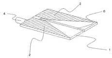
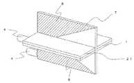
以下、この発明の実施の形態1について図1〜11を用いて説明する。図3(a)は第1テーパスロットアンテナの表面(一主面)図であり、他の主面に形成された第1ストリップ導体が透視されている。図3(b)は第1テーパスロットアンテナの側面図、図3(c)は第1テーパスロットアンテナの裏面(他の主面)図、図5(a)は第2テーパスロットアンテナの表面(一主面)図であり、他の主面に形成された第2ストリップ導体が透視されている。図5(b)は第2テーパスロットアンテナの側面図、図5(c)は第2テーパスロットアンテナの裏面(他の主面)図、図6(a)は第1テーパスロットアンテナと第2テーパスロットアンテナとの嵌合前の模式図、図10(a)はスロット線路、図10(b)はテーパスロットアンテナの調整方法説明図(物理長)、図10(c)はテーパスロットアンテナの調整方法説明図(スロット線路幅)、図11(a)(b)はテーパスロットアンテナの調整方法説明図(物理長)である。
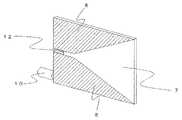
図1〜11において、1は第1の誘電率を有する第1基板、2は第1基板1の一主面に形成され、第1基板1の一端から他端に向かってテーパ状に導体パターンが縮小する第1テーパスロット部であり、第1テーパスロット部2のスロットが第1基板1の一端から他端に向かってテーパ状に拡幅しているともいえる。特に、拡幅の度合いが少ない第1基板1の一端側を第1スロット(第1スロット線路)と称す。3は第1テーパスロット部2の給電点に対向して第1基板1の他の主面に形成され、第1テーパスロット部2と第1基板1を挟んで交差する第1ストリップ導体、4は第1基板1の一端側に形成され、第1外部導体が第1基板1の一端側で第1テーパスロット部2と電気的に接続された第1同軸コネクタ、5は第1同軸コネクタ4の中心導体で、第1基板1の一端側から第1基板1の他の主面へ延び、第1ストリップ導体3と電気的に接続された第1中心導体、6は第1基板1の他端から第1ストリップ導体3と第1テーパスロット部2とが第1基板1を挟んで交差する手前まで延びた第1基板1に形成された第1切り欠き部である。図中、同一符号は、同一又は相当部分を示しそれらについての詳細な説明は省略する。 1 to 11, 1 is a first substrate having a first dielectric constant, 2 is formed on one main surface of the
図1〜11において、7は第2の誘電率を有する第2基板、8は第2基板7の一主面に形成され、第2基板7の一端から他端に向かってテーパ状に導体パターンが縮小する第2テーパスロット部であり、第2テーパスロット部8のスロットが第2基板7の一端から他端に向かってテーパ状に拡幅しているともいえる。特に、拡幅の度合いが少ない第2基板7の一端側を第2スロット(第2スロット線路)と称す。9は第2テーパスロット部8の給電点に対向して第2基板7の他の主面に形成され、第2テーパスロット部8と第2基板7を挟んで交差する第2ストリップ導体、10は第2基板7の一端側に形成され、第2外部導体が第2基板7の一端側で第2テーパスロット部8と電気的に接続された第2同軸コネクタ、11は第2同軸コネクタ10の中心導体で、第2基板7の一端側から第2基板7の他の主面へ延び、第1ストリップ導体3と電気的に接続された第2中心導体、12は第2基板7の一端から第2ストリップ導体9と第2テーパスロット部8とが第2基板7を挟んで交差する手前まで延びた第2基板7に形成された第2切り欠き部、13は第1基板1と第2基板とを固定する基板固定用接着剤、14は第2基板7の両面、又は、一主面若しく他の主面のいずれか一方に形成され、第1基板1が嵌合される溝部、15は第2基板7の両面、又は、一主面若しく他の主面のいずれか一方に形成され、第1基板1が嵌合される支持部、16はスロット線路である。図中、同一符号は、同一又は相当部分を示しそれらについての詳細な説明は省略する。 1 to 11, 7 is a second substrate having a second dielectric constant, 8 is formed on one main surface of the
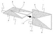
まず、構成及び動作について説明する。図1に記載された実施の形態1に係るテーパスロットアンテナは、第1テーパスロットアンテナと第2テーパスロットアンテナとを嵌合させることにより構成される。第1テーパスロットアンテナは、図2及び図3(a)に示す第1基板1の一主面上に形成された第1テーパスロット部2により第1基板1の一端から他端に向けてテーパ状に開口が拡幅していく第1スロットへ、図3(c)に示す第1基板1の他の主面上に形成された第1ストリップ導体3を信号導体とし、第1テーパスロット部2を接地導体として構成された第1マイクロストリップ線路から給電されるアンテナである。第1スロットと第1ストリップ導体3は第1基板1を挟んで交差した位置に置かれる。第1切り欠き部6は、第1基板1の他端から第1スロットの中心に沿って形成され、第1ストリップ導体3の手前まで設けられている。また、第1ストリップ導体3は、屈曲部を有しており、第1スロットと交差していない部分が折れ曲がり、第1基板1の一端に固定された第1同軸コネクタ4に向かって延びている。第1同軸コネクタ4を第1基板1の側面に設ける場合は、第1ストリップ導体3(第1中心導体5)に屈曲部を設ける必要は必ずしもない。なお、屈曲部の形状は、その部分での電波の反射がアンテナの動作と問題とならないようにインピーダンス整合がとれておれば、直角状の屈曲部でもよいし、円弧の屈曲でもよい。そして、第1ストリップ導体3は、第1同軸コネクタ4の第1中心導体5と電気的に接続される(図3(b)(c))。もちろん、第1中心導体5を延伸させ、屈曲部を設けることにより、第1中心導体5と第1テーパスロット部2とにより第1マイクロストリップ線路を構成してもよい。言い換えると、第1ストリップ導体3と第1中心導体5とが一体であるともいえる。 First, the configuration and operation will be described. The tapered slot antenna according to
第2テーパスロットアンテナは、図4及び図5(a)に示す第2基板7の一主面上に形成された第2テーパスロット部8により第2基板7の一端から他端に向けてテーパ状に開口が拡幅していく第2スロットへ、図5(c)に示す第2基板7の他の主面上に形成された第2ストリップ導体9を信号導体とし、第2テーパスロット部8を接地導体として構成された第2マイクロストリップ線路から給電されるアンテナである。第2スロットと第2ストリップ導体9は第2基板7を挟んで交差した位置に置かれる。第2切り欠き部12は、第2基板7の一端から第2スロットの中心に沿って形成され、第2ストリップ導体9の手前まで設けられている。また、第2ストリップ導体9は、屈曲部を有しており、第2スロットと交差していない部分が折れ曲がり、第2基板7の一端に固定された第2同軸コネクタ10に向かって延びている。ここで、第2同軸コネクタ10を第2基板7の側面に設ける場合は、第2ストリップ導体9(第2中心導体11)に屈曲部を設ける必要は必ずしもない。なお、屈曲部の形状は、その部分での電波の反射がアンテナの動作と問題とならないようにインピーダンス整合がとれておれば、直角状の屈曲部でもよいし、円弧の屈曲でもよい。そして、第2ストリップ導体9は、第2同軸コネクタ10の第2中心導体11と電気的に接続される(図5(b)(c))。もちろん、第2中心導体11を延伸させ、屈曲部を設けることにより、第2中心導体11と第2テーパスロット部8とにより第2マイクロストリップ線路を構成してもよい。言い換えると、第2ストリップ導体9と第2中心導体11とが一体であるともいえる。 The second taper slot antenna is tapered from one end of the
図6及び図7を用いて、実施の形態1に係るテーパスロットアンテナの組立に関して説明する。図6に示すように、第1テーパスロットアンテナと第2テーパスロットアンテナとを90°ずらして、それぞれの第1切り欠き部6と第2切り欠き部12とを対向させて、第1基板1に第2基板7を挿入、又は、第2基板7に第1基板1を挿入して、第1基板1と第2基板7とを嵌合させる。つまり、第1基板1と第2基板7とは90°で交差することになる。次に、導体で形成された第1テーパスロット部2と導体で形成された第2テーパスロット部とを交差させ、第2テーパスロット部8の給電点を第1テーパスロット部2の給電点よりも第1テーパスロット部2及び前記第2テーパスロット部8のスロット(第1スロット,第2スロット)が拡幅している方向側に配置したことになる。そして、図7に示すように、基板固定用接着剤13を用いて、嵌合後の第1基板1と第2基板7と固定する。基板固定用接着剤13は、第1基板1及び第2基板7との他端側に塗布しているように(図7)、第1基板1及び第2基板7とが嵌合している部分の一部に塗布してもよいし、第1基板1及び第2基板7とが嵌合している部分の全体に塗布してもよい。つまり、第1基板1及び第2基板7との嵌合が維持できればよいので、適宜、基板固定用接着剤13の使用量や塗布範囲・塗布位置を決めればよい。以上のようにして、実施の形態1に係るテーパスロットアンテナが組立てられる。第1基板1及び第2基板7との固定手段は、基板固定用接着剤13以外にも、セロハンテープやビニールテープなどでもよい。また、基板固定用接着剤13などの固定手段を用いなくても、第1基板1及び第2基板7との嵌合が維持できれば、基板固定用接着剤13などの固定手段を使用する必要はない。 The assembly of the tapered slot antenna according to the first embodiment will be described with reference to FIGS. As shown in FIG. 6, the first taper slot antenna and the second taper slot antenna are shifted by 90 ° so that the
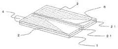
図8及び図9は、前述した基板固定用接着剤13などの固定手段以外の第1基板1と第2基板7とを固定する手段を示しており、第1テーパスロットアンテナが嵌合される前の状態を示している。図8に記載の第2テーパスロットアンテナの一主面と他の主面との両面には、溝部14が形成されている。この溝部14は、第2スロットが縮小・拡幅している方向であって、第2スロットの中心、つまり、第1基板1が嵌合する位置に配置され、少なくとも第2基板7の他端から第2切り欠き部12まで溝が掘られている。溝部14に第1基板1の第1切り欠き部6が嵌合されることにより、実施の形態1に係るテーパスロットアンテナが構成される。溝部14は、第2基板7の一主面又は他の主面のいずれか一方だけに設けてよいし、前述した基板固定用接着剤13などの固定手段と併用してもよい。また、溝部14の形状は、図8に示すような矩形以外にも、三角形などの多角形型や円弧型の窪みでもよいが、その場合も第1基板1の第1切り欠き部6の断面形状が溝部14に嵌合可能な形状である必要がある。つまり、第1基板1の第1切り欠き部6の断面形状と溝部14とが嵌合可能であれば、段差状の溝部14でも斜めに傾いた溝部14でも構わない。さらに、溝部14を第1基板1側に設けてもよいし(図示は省略する)、第1基板1側と第2基板7側の両方に設けてもよい。溝部14を第1基板1側に設ける場合、溝部14(第1基板1側)は、第1スロットが縮小・拡幅している方向であって、第1スロットの中心、つまり、第2基板7が嵌合する位置に配置され、少なくとも第1基板1の一端から第1切り欠き部6まで溝が掘られている。もちろん、切り欠き部の長さが長い方である第1切り欠き部6に嵌合される第2基板7に形成された溝部14の方が、第1基板1に形成された溝部14よりも、基板を支持する機能が高いことはいうまでもない。したがって、第1基板1及び第2基板7との嵌合が維持できればよいので、適宜、溝部14の設置範囲や設置位置を決めればよい。 FIGS. 8 and 9 show means for fixing the
図9に記載の第2テーパスロットアンテナの一主面と他の主面との両面には、誘電体ブロックで形成された支持部15が貼り付けられている。この支持部15は、この支持部15は、第2スロットが縮小・拡幅している方向であって、第2スロットの中心、つまり、第1基板1が嵌合する位置の横に配置されている。第1基板1と第2基板7とが嵌合され、支持部15が第1基板1を支持することにより、実施の形態1に係るテーパスロットアンテナが構成される。支持部15は、第2基板7の一主面又は他の主面のいずれか一方だけに設けてよいし、前述した基板固定用接着剤13などの固定手段と併用してもよい。また、支持部15の位置は、図9に示すような第2基板7の他端側以外にも、第2スロットが縮小・拡幅している方向であって、第2スロットの中心、つまり、第1基板1が嵌合する位置の横に配置されておれば、第2基板7の一端から他端に亘って形成してもよいし、第2基板7の一端側でもよい。もちろん、第2基板7の一端側及び他端以外の場所でもよい。例えば、第2基板の中央などが考えられる。なお、図9では、第2基板7の支持部15が、第1基板1が嵌合される位置の両横に配置されているが、実施の形態1に係るテーパスロットアンテナを設置する際に、第1基板1の下に来る側だけに支持部15を形成してもよい。具体的には、図9において、第2同軸コネクタ10を下側にして、実施の形態1に係るテーパスロットアンテナを設置するとした場合は、図9において、下側の方の支持部15だけを形成することになる。さらに、支持部15を第1基板1側に設けてもよいし(図示は省略する)、第1基板1側と第2基板7側の両方に設けてもよい。つまり、第1基板1及び第2基板7との嵌合が維持できればよいので、適宜、支持部15の設置範囲や設置位置を決めればよい。但し、第1基板1側と第2基板7側の両方に支持部15を設ける場合は、第1基板1側の支持部15と第2基板7側の支持部15とが、第1基板1と第2基板7との嵌合するときに干渉しないように、第1基板1側の支持部15と第2基板7側の支持部15とを配置する必要がある。 Support portions 15 formed of dielectric blocks are attached to both the main surface and the other main surface of the second tapered slot antenna shown in FIG. The support portion 15 is arranged in the direction in which the second slot is contracted and widened, and is arranged at the center of the second slot, that is, next to the position where the
このような、実施の形態1に係るテーパスロットアンテナは、第1テーパスロットアンテナと第2テーパスロットアンテナとを直交させて構成するが、このテーパスロットアンテナから電波を送信する場合、第1同軸コネクタ4及び第2同軸コネクタ10に、それぞれ同相の信号を給電する。第1同軸コネクタ4に給電された信号は第1マイクロストリップ線路を伝搬し、第1スロットに給電する。第1スロット(第1スロット線路)に給電された信号は第1テーパスロット部2を伝搬して放射する。第2同軸コネクタ10に給電された信号も同様に、第2マイクロストリップ線路、第2スロット(第2スロット線路)、第2テーパスロットテーパ部8を伝搬して、放射する。 Such a taper slot antenna according to the first embodiment is configured by making the first taper slot antenna and the second taper slot antenna orthogonal to each other. When radio waves are transmitted from the taper slot antenna, the first coaxial connector is used. 4 and the second
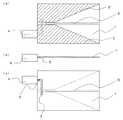
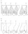
続いて、図10及び図11を用いて、実施の形態1に係るテーパスロットアンテナの調整方法について説明する。図10は、実施の形態1に係るテーパスロットアンテナの基板上に設けたスロット線路を示している。つまり、第1基板1の場合は第1スロット線路であり、第2基板7の場合は第2スロット線路である。スロット線路は基板に使用される誘電体の誘電率が高いほど電気長が長くなる。また、スロット幅Wが狭いほど電気長が長くなる。さらに、基板の厚さtが厚いほど電気長が長くなる。つまり、この三つの要素が複合されて、スロット線路の電気長が決まる。この例を図10(b)(c)に示す。図10(b)はスロット線路の物理長Lに対する電気長を、基板の誘電率が2および5の場合について示す。図10(b)における条件は、周波数10GHz、誘電体基板の基板厚t=2mm、スロット線路幅w=0.2mmである。図10(b)より物理的に同じ寸法でも誘電率を調整することで電気長を調整することができる。図10(c)はスロット線路の幅Wに対するこれらの電気長差を示す。図10(c)における条件は、周波数10GHz、誘電体基板の基板長(スロット線路が延びている方向)L=20mm、誘電体基板の基板厚t=2mm、誘電体基板の誘電率(比誘電率)5である。図10(c)より同じ物理長、同じ誘電率でもスロット線路の幅Wを調整することで電気長を調整することができることが分かる。第1テーパスロットアンテナ及び第2テーパスロットアンテナから放射する信号が下記の数1及び数2の関係を満たすように基板の誘電率やスロット線路の幅などを調整することで電気長を調整し、円偏波の信号を放射することができる。なお、数1及び数2において、EXは第1テーパスロットアンテナから放射する信号を示し、EYは第2テーパスロットアンテナから放射する信号を示す。Jは虚数単位である。Next, a method for adjusting a tapered slot antenna according to

次に、図11を用いて、第1テーパスロットアンテナと第2スロットアンテナとのスロット線路の幅を固定した場合の実施の形態1に係るテーパスロットアンテナの調整方法の具体例を説明する。図11に示す誘電率2を第1基板の第1の誘電率とし、誘電率5を第2基板の第2の誘電率としたときに、図11(a)の矢印で示した物理長Lを選択すれば、電気長の差が90°となるので、第1同軸コネクタ4及び第2同軸コネクタ10に、それぞれ同相の信号を給電しても実施の形態1に係るテーパスロットアンテナは、所望の円偏波の電波を放射可能であることが分かる。もちろん、誘電率が高くなるにつれ、図11の傾きが大きな特性があることが分かるので、第1の誘電率と第2の誘電率とが「2」や「5」の基板を準備できなくても、実施の形態1に係るテーパスロットアンテナは調整が可能であることが分かる。物理長Lに制約がある場合は、図10(c)に示すスロット線路幅も合わせて調整してやればよい。もちろん、第1の誘電率と第2の誘電率とを固定して、スロット線路幅だけで、電気長の差が90°になるように調整してもよい。 Next, a specific example of the method for adjusting the tapered slot antenna according to the first embodiment when the widths of the slot lines of the first tapered slot antenna and the second slot antenna are fixed will be described using FIG. When the
実施の形態1に係るスロットテーパアンテナは、第1スロット線路と第2スロット線路との給電点は、第2テーパスロット部8(第2スロット線路)の給電点を第1テーパスロット部2(第1スロット線路)の給電点よりも第1テーパスロット部2及び第2テーパスロット部8のスロットが拡幅している方向側に配置されている。つまり、第2テーパスロットアンテナにおける第2マイクロストリップ線路が、第1テーパスロットアンテナにおける第1マイクロストリップ線路よりも長い。この長さの差が無視できる程度あれば、図10及び図11(a)を用いた説明した調整を行えば、第1同軸コネクタ4及び第2同軸コネクタ10に、それぞれ同相の信号を給電することにより、所望の円偏波がテーパスロットアンテナから放射されるが、第1マイクロストリップ線路と第2マイクロストリップ線路との差が無視できないぐらいに大きい場合は、これを考慮して調整する必要がある。第2マイクロストリップ線路が第1マイクロストリップ線路よりも長い場合は、その長さの差の分だけ、給電点において、第1マイクロストリップ線路の位相が進むことになる。その進んだ位相を図11では点線で示している。つまり、点線は、誘電率2の基板(第1基板)にマイクロストリップ線路の長さの差による位相の違いを反映させたものである。あとは、この点線と誘電率5の直線で、図11(b)の矢印で示した物理長Lを選択すれば、電気長の差が90°となるので、第1同軸コネクタ4及び第2同軸コネクタ10に、それぞれ同相の信号を給電しても所望の円偏波の電波を放射可能なテーパスロットアンテナが得られることが分かる。したがって、実施の形態1に係るテーパスロットアンテナは、第1基板1の第1の誘電率と第1テーパスロット部2の一端から他端までの長さ(物理長L)と、第2基板7の第2の誘電率と第2テーパスロット部8の一端から他端まで長さ(物理長L)とをそれぞれ調整し、第1テーパスロット部2によるアンテナ(第1テーパスロットアンテナ)と第2テーパスロット部8によるアンテナ(第2テーパスロットアンテナ)との位相差を90°にすることが可能である。 In the slot taper antenna according to the first embodiment, the feed point between the first slot line and the second slot line is the feed point of the second taper slot part 8 (second slot line). The slots of the first
実施の形態2.
実施の形態1では、第1テーパスロット部2と第2テーパスロット部9とが基板上に形成されたものを説明したが、実施の形態2では、その変形例を説明する。実施の形態1と共通の部分は、その説明を省略する。この発明の実施の形態2について図12〜20を用いて説明する。図14(a)は第1テーパスロットアンテナの表面(一主面)図であり、他の主面に形成された第1ストリップ導体が透視されている。図14(b)は第1テーパスロットアンテナの側面図、図14(c)は第1テーパスロットアンテナの裏面(他の主面)図、図16(a)は第2テーパスロットアンテナの表面(一主面)図であり、他の主面に形成された第2ストリップ導体が透視されている。図16(b)は第2テーパスロットアンテナの側面図、図16(c)は第2テーパスロットアンテナの裏面(他の主面)図、図20(a)は第1テーパスロットアンテナの表面(一主面)図であり、一主面に形成された第1テーパスロット部と他の主面に形成された第1ストリップ導体が透視されている。図20(b)は第1テーパスロットアンテナの側面図、図20(c)は第1テーパスロットアンテナの裏面(他の主面)図である。
In the first embodiment, the first tapered
図12〜20において、17は第1の誘電率を有し、第1スロット線路近傍に形成された第1基板、18は第1基板1の一主面に形成され、第1基板1の一端から他端に向かってテーパ状に導体パターンが縮小する第1テーパスロット部であり、第1テーパスロット部18のスロットが第1基板1の一端から他端に向かってテーパ状に拡幅しているともいえる。特に、拡幅の度合いが少ない第1基板17の一端側を第1スロット(第1スロット線路)と称し、第1スロット以外の部分の下部には第1基板17がない。19は第2の誘電率を有し、第2スロット線路近傍に形成された第2基板、20は第2基板7の一主面に形成され、第2基板7の一端から他端に向かってテーパ状に導体パターンが縮小する第2テーパスロット部であり、第2テーパスロット部20のスロットが第2基板19の一端から他端に向かってテーパ状に拡幅しているともいえる。特に、拡幅の度合いが少ない第2基板19の一端側を第1スロット(第1スロット線路)と称し、第1スロット以外の部分の下部には第1基板17がない。なお、第2基板19には、第2基板19の一端から第2ストリップ導体9と第2テーパスロット部20とが第2基板19を挟んで交差する手前まで延びた第2切り欠き部12が形成されている。21は第1基板1上に形成された誘電体層である。図面上では、実施の形態1と比較のために第1テーパスロット部18と第2テーパスロット部20とは厚みが薄いものを図示しているが、実際は、基板なしで自重に耐え得る強度を有する導体とその厚みを必要とする。図中、同一符号は、同一又は相当部分を示しそれらについての詳細な説明は省略する。 12 to 20, 17 has a first dielectric constant, a first substrate formed in the vicinity of the first slot line, and 18 formed on one main surface of the
図12〜16に記載のテーパスロットアンテナは、実施の形態1に係るテーパスロットアンテナと異なり、給電点や同軸コネクタを固定する箇所以外は、基板を設けない構成となっている。給電点以外に基板がないために、図10〜11で説明したテーパスロットアンテナの調整方法では、ともに誘電率1として誘電率を固定して、それ以外の要素で調整する必要が有り、調整代(しろ)が制限されてしまう。しかし、第1テーパスロット部18と第2テーパスロット部20とが板金などの金属板加工技術で容易に製造可能であるという効果や、第1テーパスロットアンテナと第2テーパスロットアンテナとを嵌合させる際に、図13及び図14に示すように、第1テーパスロットアンテナ側に切り欠き部を形成する必要がなく、第1基板17のスロット部分に、第2基板19の第2切り欠き部12(図15,図16参照)を嵌合させるだけで図12に記載のテーパスロットアンテナが得られるという効果がある。また、基板の使用が給電点付近に留められているので、基板と第1テーパスロット部,第2テーパスロット部の導体との線膨張率の違いによる使用環境の制限が緩和されるという効果もある。なお、給電点には基板(第1基板17,第2基板19)があるので、図10〜11で説明した調整を第1テーパスロット部,第2テーパスロット部の下部の誘電率1と第1基板17,第2基板19の誘電率(第1の誘電率,第2の誘電率)との実効的な誘電率で調整する必要がある場合もある。もちろん、第1テーパスロットアンテナの第1基板17に第1基板17の他端から第1ストリップ導体3と第1テーパスロット部18とが第1基板17を挟んで交差する手前まで延びた第1切り欠き部6を形成してもよい。つまり、第1基板17の切り欠き部6と第2基板19の切り欠き部12とを嵌合させて、実施の形態2に係るテーパスロットアンテナを構成してもよい。 Unlike the tapered slot antenna according to the first embodiment, the tapered slot antenna illustrated in FIGS. 12 to 16 has a configuration in which a substrate is not provided except for a portion where a feeding point and a coaxial connector are fixed. Since there is no substrate other than the feed point, the adjustment method of the tapered slot antenna described with reference to FIGS. 10 to 11 requires both the dielectric constant to be fixed as the
図17に記載のテーパスロットアンテナは、第1テーパスロットアンテナに図13及び図14に記載のもの、第2テーパスロットアンテナに図4及び図5に記載したものを採用した構造となっており、図12〜16に記載のテーパスロットアンテナと同様に、第1テーパスロットアンテナ側が誘電率1として誘電率を固定して、それ以外の要素で調整する必要が有り、調整代(しろ)が制限されてしまうが、第1テーパスロットアンテナと第2テーパスロットアンテナとを嵌合させる際に、第1テーパスロットアンテナ側に切り欠き部を形成する必要がなく、第1基板17のスロット部分に、第2基板7の第2切り欠き部12を嵌合させるだけで図12に記載のテーパスロットアンテナが得られるという効果ある。なお、第2基板7があるので、図10〜11で説明した調整を第2テーパスロット部の下部の誘電率1と第2基板7の誘電率(第2の誘電率)との実効的な誘電率で調整する必要がある場合もある。もちろん、第1テーパスロットアンテナの第1基板17に第1基板17の他端から第1ストリップ導体3と第1テーパスロット部18とが第1基板17を挟んで交差する手前まで延びた第1切り欠き部6を形成してもよい。つまり、第1基板17の切り欠き部6と第2基板7の切り欠き部12とを嵌合させて、実施の形態2に係るテーパスロットアンテナを構成してもよい。The tapered slot antenna shown in FIG. 17 has a structure in which the first tapered slot antenna shown in FIGS. 13 and 14 is adopted, and the second tapered slot antenna shown in FIGS. 4 and 5 is adopted. Similar to the taper slot antenna described in FIGS. 12 to 16, the first taper slot antenna side needs to have a dielectric constant of 1 and the dielectric constant needs to be adjusted, and adjustment is performed with other factors, and the adjustment margin is limited. However, when fitting the first taper slot antenna and the second taper slot antenna, there is no need to form a notch on the first taper slot antenna side, and the slot portion of the
図18〜20に記載のテーパスロットアンテナは、実施の形態1に係るテーパスロットアンテナの第1基板1上に誘電体層21を追加したものである。この誘電体層21を第1基板1に形成することにより、第1テーパスロット部2の導体が第1基板1から剥離することを防ぐ効果がある。また、第1基板1と第2基板7との固定の補助としても機能する。このことから、誘電体層21は、図9に記載の支持部15のうち、上側の方の支持部15が大型化したものとも見なせる。また、誘電体層21は、第1基板1上であって、第1切り欠き部6の開口を妨げない位置に形成されておればよく、図19及び図20に示すように、第1スロット付近は、第1基板7を露出させていてもよい。誘電体層21に第1基板1の第1切り欠き部6同じ形状の切り欠き部を形成せいた場合は、第2基板7の切り欠き部12の寸法は、誘電体層21の厚みを考慮した寸法に設計する必要がある。もちろん、第2基板7に誘電体層を形成してもよいし、第1基板1と第2基板7との両方に誘電体層を形成してもよい。また、図10〜11で説明したテーパスロットアンテナの調整方法は、誘電体層(誘電体層21)の誘電率も考慮して行う必要があることはいうまでもない。The taper slot antenna described in FIGS. 18 to 20 is obtained by adding a
実施の形態3.
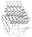
実施の形態1及び2では、円偏波を放射するテーパスロットアンテナの最小単位を説明したが、実施の形態3では、実施の形態1及び2で説明したテーパスロットアンテナを格子状に複数配列し、第1テーパスロット部同士及び第2テーパスロット部同士を隣り合わせにしたテーパスロットアレイアンテナ装置について説明する。なお、実施の形態1に係るテーパスロットアンテナのうち、図1〜7で説明したものを用いて実施の形態3を説明するが、他の実施の形態1及び2に係るテーパスロットアンテナも適用可能であることはいうまでもない。また、テーパスロットアレイアンテナ装置の構成・動作や調整方法も同様に、実施の形態1及び2に記載のものと同様であるので、実施の形態3に係るテーパスロットアレイアンテナ装置の構成を中心に記載する。この発明の実施の形態3について図21〜24を用いて説明する。図21〜24において、23は第1の誘電率を有する第1基板、24は第1テーパスロット部2同士が隣り合わせになった状態の第1テーパスロット部であり、第1テーパスロット部2同士が背中合わせになって導体パターンが連続している。第1テーパスロット部24がアレイ状に複数並んでいるものを第1テーパスロット部群と称する。なお、第1テーパスロット部群の両端部は、第1テーパスロット部2であるが、以下、便宜上、第1テーパスロット部群は、第1テーパスロット部24が横に並んでいるものとして説明する。25は第2の誘電率を有する第2基板、26は第2テーパスロット部8が隣り合わせになった第2テーパスロット部あり、第2テーパスロット部8同士が背中合わせになって導体パターンが連続している。第2テーパスロット部26がアレイ状に複数並んでいるものを第2テーパスロット部群と称する。なお、第2テーパスロット部群の両端部は、第2テーパスロット部8であるが、以下、便宜上、第2テーパスロット部群は、第2テーパスロット部26が横に並んでいるものとして説明する。
In
図24において、27は第1基板23を固定する基板固定板、28は第2基板25を固定する基板固定板、29は第1基板23の外周にあって、第1基板23を固定する枠板、30は第2基板25の外周にあって、第2基板25を固定する枠板である。第1基板23には、第1スロットごとに第1切り欠き部6が複数形成され、第2基板25には、第2スロットごとに第2切り欠き部12が複数形成されている。実施の形態に係るテーパスロットアレイアンテナ装置は、複数の第1基板23と複数の第2基板25とを格子状の嵌合させることにより形成される。また、図24では省略しているが、枠板29は第1基板23の左右に、枠板30は第2基板25の上下にそれぞれ設けられている。図中、同一符号は、同一又は相当部分を示しそれらについての詳細な説明は省略する。 In FIG. 24, 27 is a substrate fixing plate for fixing the
図21には、嵌合前の第1基板23を示しており、図21(a)は他の主面に複数形しえされた第1ストリップ導体3が透視されている。図21(b)は第1切り欠き部6の形状を明瞭化した図である。このように、一端から他端に向かってテーパ状に導体パターンが縮小する第1テーパスロット部2が横に複数配列され、隣り合う第1テーパスロット部同士の導体パターンが連続(第1テーパスロット部24)した第1テーパスロット部群が第1基板23の一主面に形成されている。また、第1テーパスロット部群の給電点に対向して第1基板23の他の主面に形成され、第1テーパスロット部群24(2)と第1基板23を挟んで交差する第1ストリップ導体3が第1テーパスロット部群24(2)ごとに設けられた第1ストリップ導体群が、それぞれ、第1基板23の一端側に形成され、第1中心導体5が第1基板23の他の主面へ延び、第1外部導体が第1基板23の一端側で第1テーパスロット部23と電気的に接続された第1同軸コネクタ4が第1テーパスロット部23ごとに設けられた第1同軸コネクタ群と電気的に接続されている。 FIG. 21 shows the
図22には、嵌合前の第2基板25を示しており、図22(a)は他の主面に複数形しえされた第2ストリップ導体9が透視されている。図22(b)は第2切り欠き部12の形状を明瞭化した図である。このように、一端から他端に向かってテーパ状に導体パターンが縮小する第2テーパスロット部8が横に複数配列され、隣り合う第2テーパスロット部同士の導体パターンが連続(第2テーパスロット部26)した第2テーパスロット部群が第2基板25の一主面に形成されている。また、第2テーパスロット部群26の給電点に対向して第2基板25の他の主面に形成され、第2テーパスロット部群26と第2基板25を挟んで交差する第2ストリップ導体9が第2テーパスロット部群26ごとに設けられた第2ストリップ導体群が、それぞれ、第2基板25の一端側に形成され、第2中心導体11が第2基板25の他の主面へ延び、第2外部導体が第2基板25の一端側で第2テーパスロット部26と電気的に接続された第2同軸コネクタ10が第2テーパスロット部26ごとに設けられた第1同軸コネクタ群と電気的に接続されている。 FIG. 22 shows the
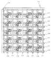
図23は、テーパスロットアレイ装置を構成する複数の第1基板23と複数の第2基板25とを並べた基板アレイを示す図である。第1基板23と第2基板25とを格子状に複数配列し、第1基板23に形成された複数の第1切り欠き部6ごとにそれぞれの第2切り欠き部12を嵌合させた複数の第2基板25と、第2基板25に形成された複数の第2切り欠き部12ごとにそれぞれの第1切り欠き部6を嵌合させた複数の第1基板23とを格子状に交差させた状態を示している。格子状に交差させた状態を明瞭にするために、第1同軸コネクタ4及び第2同軸コネクタ10や導体パターンは省略している。なお、点線で囲われた一つの第1テーパスロットと第2テーパスロットアンテナに関しては、拡大図で導体パターンを示している。また、この拡大図として取り上げられている一枚の第1基板23と第2基板25は、嵌合状態を明瞭にするために、図23上部の第1基板23と第2基板25を格子状に複数配列した基板アレイから外されたものであり、この第1基板23と第2基板25とから、一枚の第1基板23に複数形成された切り欠き部6にそれぞれ複数の第2基板25が嵌合されている様子と、一枚の第2基板25に複数形成された切り欠き部12にそれぞれ複数の第1基板23が嵌合されている様子とが分かる。さらに、第1切り欠き部6群の後方にある符号を付していない切り欠き部は、後述する基板固定板27が嵌合されるもので、第2切り欠き部12群の間にある符号を付していない切り欠き部は、後述する基板固定板28が嵌合されるものである。 FIG. 23 is a diagram showing a substrate array in which a plurality of
さらに、詳しくテーパスロットアレイアンテナ装置の構造を説明すると、図面(図23)上、一枚の第1基板23の端から端まで(複数の第1切り欠き部6が並んでいる方向の一端から他端まで)の第1切り欠き部6の一つ一つに、それぞれ第2基板25が一枚ずつ嵌合されているおり、このような第1基板23が複数枚等間隔で並べられている。一枚の第2基板25の端から端まで(複数の第2切り欠き部12が並んでいる方向の一端から他端まで)の第1切り欠き部12の一つ一つに、それぞれ第1基板23が一枚ずつ嵌合されているおり、このような第2基板25が複数枚等間隔で並べられている。つまり、このような複数枚等間隔で並べられた第1基板23と複数枚等間隔で並べられた第2基板25とが、格子状のテーパスロットアレイアンテナ装置を形成している。 Further, the structure of the taper slot array antenna device will be described in detail. From the end of one sheet of the
図24は、図23で示したテーパスロットアレイ装置の基板アレイの強度を確保するための構造を第1同軸コネクタ4群,第2同軸コネクタ10群側から示した図(テーパスロットアレイ装置の放射面の反対面から見た図)である。詳細構造は、以下の通りである。基板アレイは、複数の第1基板23をそれぞれ第2基板25と平行に並べた複数の基板固定板27で固定し、複数の第2基板25をそれぞれ第1基板23と平行に並べた複数の基板固定板28で固定して構成されている。基板固定板27は、前述の第1基板23に形成された切り欠き部に挿入(嵌合)され、基板固定板28は、前述の第2基板25に形成された切り欠き部に挿入(嵌合)されている。なお、基板固定板27と基板固定板28とに切り欠き部を形成して、基板固定板27と基板固定板28とを嵌合させている。このようにして、基板固定板27と基板固定板28に固定した基板アレイの周囲を枠板29と枠板30で固定する。 FIG. 24 is a diagram showing a structure for ensuring the strength of the substrate array of the tapered slot array device shown in FIG. 23 from the first
具体的には、複数の第1基板23の端部が枠板29により固定され、複数の第2基板25の端部が枠板30により固定されている。そして、枠板29と枠板30とが接続されている。枠板29と枠板30とは一体であってもよい。枠板29と枠板30とが一体の場合、一体の枠板に基板アレイを挿入することにより、基板アレイを一体の枠板により固定するなどが考えられる。ここで、図24のように、を枠体30に固定、基板固定板28を枠体29に固定してもよい。なお、テーパスロットアレイ装置は、図23の基板アレイだけで構成されているとしてもよいし、図24の基板アレイに基板固定板27,28と枠板29,30を含めて構成されているとしてもよい。もちろん、基板アレイは、基板固定板27及び基板固定板28を含めて基板アレイとしてもよいことはいうまでもない。Specifically, the end portions of the plurality of
1・・第1基板、2・・第1テーパスロット部、3・・第1ストリップ導体、4・・第1同軸コネクタ、5・・第1中心導体、6・・第1切り欠き部、7・・第2基板、8・・第2テーパスロット部、9・・第2ストリップ導体、10・・第2同軸コネクタ、11・・第2中心導体、12・・第2切り欠き部、13・・基板固定用接着剤、14・・溝部、15・・支持部、16・・スロット線路、17・・第1基板、18・・第1テーパスロット部、19・・第2基板、20・・第2テーパスロット部、21・・誘電体層、23・・第1基板、24・・第1テーパスロット部、25・・第2基板、26・・第2テーパスロット部、27・・基板固定板、28・・基板固定板、29・・枠板、30・・枠板。1 ···
Claims (10)
Translated fromJapanese一端が前記第1テーパスロット部の給電点に対向する第1ストリップ導体と、この第1ストリップ導体と前記第1テーパスロット部の給電点との間に設けられた第1基板と、一端が前記第2テーパスロット部の給電点に対向する第2ストリップ導体と、この第2ストリップ導体と前記第2テーパスロット部の給電点との間に設けられた第2基板と、前記第1基板を挟んで前記第1テーパスロット部と交差した前記第1ストリップ導体の他端に接続され、外部から信号が給電される第1同軸コネクタと、前記第2基板を挟んで前記第2テーパスロット部と交差した前記第2ストリップ導体に接続され、前記第1同軸コネクタに給電される信号と同相の信号を外部から給電される第2同軸コネクタとを備え、
前記第1基板の誘電率及び前記第2基板の誘電率、前記第1基板の厚み及び前記第2基板の厚み、前記第1テーパスロット部に設けたスロット線路の一端から他端の方向の長さ及び前記第2テーパスロット部に設けたスロット線路の一端から他端の方向の長さ、前記第1テーパスロット部に設けたスロット線路の幅及び前記第2テーパスロット部に設けたスロット線路の幅のうち、少なくとも一つを前記第1基板と前記第2基板とで異なるものとし、前記第1テーパスロット部によるアンテナと前記第2テーパスロット部によるアンテナとの位相差を90°に調整したテーパスロットアンテナ。A second taper slot formed of a conductor and formed of a first tapered slot portion and a conductorthat tapers from one end to the other end, and a conductor shape that tapers from one end to the other end. Andthe feeding point of the second taper slot part is closer to the direction in which the slots of the first taper slot part and the second taper slot part are wider than the feeding point of the first taper slot part. A tapered slot antennadisposed;
A first strip conductor having one end opposed to the feeding point of the first tapered slot portion; a first substrate provided between the first strip conductor and the feeding point of the first tapered slot portion; A second strip conductor facing the feeding point of the second taper slot portion, a second substrate provided between the second strip conductor and the feeding point of the second taper slot portion, and sandwiching the first substrate The first coaxial connector connected to the other end of the first strip conductor intersecting the first taper slot portion and fed with a signal from the outside, and the second taper slot portion across the second substrate. A second coaxial connector connected to the second strip conductor and fed with a signal in phase with the signal fed to the first coaxial connector from the outside,
The dielectric constant of the first substrate and the dielectric constant of the second substrate, the thickness of the first substrate and the thickness of the second substrate, the length from one end to the other end of the slot line provided in the first tapered slot portion And the length in the direction from one end to the other end of the slot line provided in the second taper slot portion, the width of the slot line provided in the first taper slot portion, and the slot line provided in the second taper slot portion. At least one of the widths is different between the first substrate and the second substrate, and the phase difference between the antenna by the first taper slot portion and the antenna by the second taper slot portion is adjusted to 90 °. Tapered slot antenna.
一端が前記第1テーパスロット部の給電点に対向する第1ストリップ導体と、この第1ストリップ導体と前記第1テーパスロット部の給電点との間に設けられた第1基板と、一端が前記第2テーパスロット部の給電点に対向する第2ストリップ導体と、この第2ストリップ導体と前記第2テーパスロット部の給電点との間に設けられた第2基板と、前記第1基板を挟んで前記第1テーパスロット部と交差した前記第1ストリップ導体の他端に接続され、外部から信号が給電される第1同軸コネクタと、前記第2基板を挟んで前記第2テーパスロット部と交差した前記第2ストリップ導体に接続され、前記第1同軸コネクタに給電される信号と同相の信号を外部から給電される第2同軸コネクタとを備え、
前記第1基板の誘電率が、前記第2基板の誘電率よりも低いことにより、前記第1テーパスロット部によるアンテナと前記第2テーパスロット部によるアンテナとの位相差が90°であるテーパスロットアンテナ。A second taper slot formed of a conductor and formed of a first tapered slot portion and a conductor that tapers from one end to the other end, and a conductor shape that tapers from one end to the other end. And the feeding point of the second taper slot part is closer to the direction in which the slots of the first taper slot part and the second taper slot part are wider than the feeding point of the first taper slot part. A tapered slot antenna disposed;
A first strip conductor having one end opposed to the feeding point of the first tapered slot portion; a first substrate provided between the first strip conductor and the feeding point of the first tapered slot portion; A second strip conductor facing the feeding point of the second taper slot portion, a second substrate provided between the second strip conductor and the feeding point of the second taper slot portion, and sandwiching the first substrate The first coaxial connector connected to the other end of the first strip conductor intersecting the first taper slot portion and fed with a signal from the outside, and the second taper slot portion across the second substrate. A second coaxial connector connected to the second strip conductor and fed with a signal in phase with the signal fed to the first coaxial connector from the outside,
Since the dielectric constant of the first substrate is lower than the dielectric constant of the second substrate, the tapered slot in which the phase difference between the antenna formed by the first tapered slot portion and the antenna formed by the second tapered slot portion is 90 °. antenna.
一端が前記第1テーパスロット部の給電点に対向する第1ストリップ導体と、この第1ストリップ導体と前記第1テーパスロット部の給電点との間に設けられた第1基板と、一端が前記第2テーパスロット部の給電点に対向する第2ストリップ導体と、この第2ストリップ導体と前記第2テーパスロット部の給電点との間に設けられた第2基板と、前記第1基板を挟んで前記第1テーパスロット部と交差した前記第1ストリップ導体の他端に接続され、外部から信号が給電される第1同軸コネクタと、前記第2基板を挟んで前記第2テーパスロット部と交差した前記第2ストリップ導体に接続され、前記第1同軸コネクタに給電される信号と同相の信号を外部から給電される第2同軸コネクタとを備え、
前記第1テーパスロット部に設けたスロット線路の一端から他端の方向の長さが、前記第2テーパスロット部に設けたスロット線路の一端から他端の方向の長さよりも短いことにより、前記第1テーパスロット部によるアンテナと前記第2テーパスロット部によるアンテナとの位相差が90°であるテーパスロットアンテナ。A second taper slot formed of a conductor and formed of a first tapered slot portion and a conductor that tapers from one end to the other end, and a conductor shape that tapers from one end to the other end. And the feeding point of the second taper slot part is closer to the direction in which the slots of the first taper slot part and the second taper slot part are wider than the feeding point of the first taper slot part. A tapered slot antenna disposed;
A first strip conductor having one end opposed to the feeding point of the first tapered slot portion; a first substrate provided between the first strip conductor and the feeding point of the first tapered slot portion; A second strip conductor facing the feeding point of the second taper slot portion, a second substrate provided between the second strip conductor and the feeding point of the second taper slot portion, and sandwiching the first substrate The first coaxial connector connected to the other end of the first strip conductor intersecting the first taper slot portion and fed with a signal from the outside, and the second taper slot portion across the second substrate. A second coaxial connector connected to the second strip conductor and fed with a signal in phase with the signal fed to the first coaxial connector from the outside,
The length in the direction from one end to the other end of the slot line provided in the first taper slot portion is shorter than the length in the direction from one end to the other end of the slot line provided in the second taper slot portion, A tapered slot antenna having a phase difference of 90 ° between an antenna formed by a first tapered slot portion and an antenna formed by the second tapered slot portion .
一端が前記第1テーパスロット部の給電点に対向する第1ストリップ導体と、この第1ストリップ導体と前記第1テーパスロット部の給電点との間に設けられた第1基板と、一端が前記第2テーパスロット部の給電点に対向する第2ストリップ導体と、この第2ストリップ導体と前記第2テーパスロット部の給電点との間に設けられた第2基板と、前記第1基板を挟んで前記第1テーパスロット部と交差した前記第1ストリップ導体の他端に接続され、外部から信号が給電される第1同軸コネクタと、前記第2基板を挟んで前記第2テーパスロット部と交差した前記第2ストリップ導体に接続され、前記第1同軸コネクタに給電される信号と同相の信号を外部から給電される第2同軸コネクタとを備え、
前記第1テーパスロット部に設けたスロット線路の幅が、前記第2テーパスロット部に設けたスロット線路の幅よりも広いことにより、前記第1テーパスロット部によるアンテナと前記第2テーパスロット部によるアンテナとの位相差が90°であるテーパスロットアンテナ。A second taper slot formed of a conductor and formed of a first tapered slot portion and a conductor that tapers from one end to the other end, and a conductor shape that tapers from one end to the other end. And the feeding point of the second taper slot part is closer to the direction in which the slots of the first taper slot part and the second taper slot part are wider than the feeding point of the first taper slot part. A tapered slot antenna disposed;
A first strip conductor having one end opposed to the feeding point of the first tapered slot portion; a first substrate provided between the first strip conductor and the feeding point of the first tapered slot portion; A second strip conductor facing the feeding point of the second taper slot portion, a second substrate provided between the second strip conductor and the feeding point of the second taper slot portion, and sandwiching the first substrate The first coaxial connector connected to the other end of the first strip conductor intersecting the first taper slot portion and fed with a signal from the outside, and the second taper slot portion across the second substrate. A second coaxial connector connected to the second strip conductor and fed with a signal in phase with the signal fed to the first coaxial connector from the outside,
The width of the slot line provided in the first taper slot portion is wider than the width of the slot line provided in the second taper slot portion, so that the antenna by the first taper slot portion and the second taper slot portion A tapered slotantenna having a phase difference of 90 ° with respect to the antenna.
一端が前記第1テーパスロット部の給電点に対向する第1ストリップ導体と、この第1ストリップ導体と前記第1テーパスロット部の給電点との間に設けられた第1基板と、一端が前記第2テーパスロット部の給電点に対向する第2ストリップ導体と、この第2ストリップ導体と前記第2テーパスロット部の給電点との間に設けられた第2基板と、前記第1基板を挟んで前記第1テーパスロット部と交差した前記第1ストリップ導体の他端に接続され、外部から信号が給電される第1同軸コネクタと、前記第2基板を挟んで前記第2テーパスロット部と交差した前記第2ストリップ導体に接続され、前記第1同軸コネクタに給電される信号と同相の信号を外部から給電される第2同軸コネクタとを備え、
前記第1基板の厚みが、前記第2基板の厚みよりも薄いことにより、前記第1テーパスロット部によるアンテナと前記第2テーパスロット部によるアンテナとの位相差が90°であるテーパスロットアンテナ。A second taper slot formed of a conductor and formed of a first tapered slot portion and a conductor that tapers from one end to the other end, and a conductor shape that tapers from one end to the other end. And the feeding point of the second taper slot part is closer to the direction in which the slots of the first taper slot part and the second taper slot part are wider than the feeding point of the first taper slot part. A tapered slot antenna disposed;
A first strip conductor having one end opposed to the feeding point of the first tapered slot portion; a first substrate provided between the first strip conductor and the feeding point of the first tapered slot portion; A second strip conductor facing the feeding point of the second taper slot portion, a second substrate provided between the second strip conductor and the feeding point of the second taper slot portion, and sandwiching the first substrate The first coaxial connector connected to the other end of the first strip conductor intersecting the first taper slot portion and fed with a signal from the outside, and the second taper slot portion across the second substrate. A second coaxial connector connected to the second strip conductor and fed with a signal in phase with the signal fed to the first coaxial connector from the outside,
A taper slot antenna in which a thickness of the first substrate is thinner than a thickness of the second substrate, so that a phase difference between the antenna by the first taper slot portion and the antenna by the second taper slot portion is 90 ° .
一端が前記第1テーパスロット部の給電点に対向する第1ストリップ導体と、この第1ストリップ導体と前記第1テーパスロット部の給電点との間に設けられた第1基板と、一端が前記第2テーパスロット部の給電点に対向する第2ストリップ導体と、この第2ストリップ導体と前記第2テーパスロット部の給電点との間に設けられた第2基板と、前記第1基板を挟んで前記第1テーパスロット部と交差した前記第1ストリップ導体の他端に接続され、外部から信号が給電される第1同軸コネクタと、前記第2基板を挟んで前記第2テーパスロット部と交差した前記第2ストリップ導体に接続され、前記第1同軸コネクタに給電される信号と同相の信号を外部から給電される第2同軸コネクタとを備え、
前記第1基板の誘電率が、前記第2基板の誘電率よりも低いこと、前記第1基板の厚みが、前記第2基板の厚みよりも薄いこと、前記第1テーパスロット部に設けたスロット線路の一端から他端の方向の長さが、前記第2テーパスロット部に設けたスロット線路の一端から他端の方向の長さよりも短いこと、及び、前記第1テーパスロット部に設けたスロット線路の幅が、前記第2テーパスロット部に設けたスロット線路の幅よりも広いことにより、前記第1テーパスロット部によるアンテナと前記第2テーパスロット部によるアンテナとの位相差が90°であるテーパスロットアンテナ。A second taper slot formed of a conductor and formed of a first tapered slot portion and a conductor that tapers from one end to the other end, and a conductor shape that tapers from one end to the other end. And the feeding point of the second taper slot part is closer to the direction in which the slots of the first taper slot part and the second taper slot part are wider than the feeding point of the first taper slot part. A tapered slot antenna disposed;
A first strip conductor having one end opposed to the feeding point of the first tapered slot portion; a first substrate provided between the first strip conductor and the feeding point of the first tapered slot portion; A second strip conductor facing the feeding point of the second taper slot portion, a second substrate provided between the second strip conductor and the feeding point of the second taper slot portion, and sandwiching the first substrate The first coaxial connector connected to the other end of the first strip conductor intersecting the first taper slot portion and fed with a signal from the outside, and the second taper slot portion across the second substrate. A second coaxial connector connected to the second strip conductor and fed with a signal in phase with the signal fed to the first coaxial connector from the outside,
The dielectric constant of the first substrate is lower than the dielectric constant of the second substrate, the thickness of the first substrate is thinner than the thickness of the second substrate, and the slot provided in the first tapered slot portion. The length in the direction from one end of the line to the other end is shorter than the length in the direction from one end to the other end of the slot line provided in the second taper slot portion, and the slot provided in the first taper slot portion. Since the width of the line is wider than the width of the slot line provided in the second taper slot portion, the phase difference between the antenna by the first taper slot portion and the antenna by the second taper slot portion is 90 °. Tapered slot antenna.
Priority Applications (1)
| Application Number | Priority Date | Filing Date | Title |
|---|---|---|---|
| JP2009010859AJP4924622B2 (en) | 2009-01-21 | 2009-01-21 | Tapered slot antenna and taper slot array antenna apparatus using the same |
Applications Claiming Priority (1)
| Application Number | Priority Date | Filing Date | Title |
|---|---|---|---|
| JP2009010859AJP4924622B2 (en) | 2009-01-21 | 2009-01-21 | Tapered slot antenna and taper slot array antenna apparatus using the same |
Publications (2)
| Publication Number | Publication Date |
|---|---|
| JP2010171588A JP2010171588A (en) | 2010-08-05 |
| JP4924622B2true JP4924622B2 (en) | 2012-04-25 |
Family
ID=42703303
Family Applications (1)
| Application Number | Title | Priority Date | Filing Date |
|---|---|---|---|
| JP2009010859AActiveJP4924622B2 (en) | 2009-01-21 | 2009-01-21 | Tapered slot antenna and taper slot array antenna apparatus using the same |
Country Status (1)
| Country | Link |
|---|---|
| JP (1) | JP4924622B2 (en) |
Cited By (3)
| Publication number | Priority date | Publication date | Assignee | Title |
|---|---|---|---|---|
| CN105226400A (en)* | 2015-09-16 | 2016-01-06 | 哈尔滨工业大学(威海) | A kind of wideband dual polarized phased array antenna and complete polarization Beamforming Method |
| WO2019135029A1 (en) | 2018-01-05 | 2019-07-11 | Antennium Oy | Device for receiving and re-radiating electromagnetic signal |
| CN110212314A (en)* | 2019-06-21 | 2019-09-06 | 中国电子科技集团公司第二十九研究所 | A kind of ultra-wideband high-power cross polarization array antenna and its working method |
Families Citing this family (3)
| Publication number | Priority date | Publication date | Assignee | Title |
|---|---|---|---|---|
| FR2970603A1 (en)* | 2011-01-13 | 2012-07-20 | Thomson Licensing | SLOT TYPE PRINTED DIRECTIVE ANTENNA AND NETWORK SYSTEM MULTIPLE ANTENNAES SLOT-TYPE PRINTED DIRECTIVES |
| JP6971277B2 (en)* | 2019-06-17 | 2021-11-24 | ソフトバンク株式会社 | Antennas, wireless communication devices and mobiles |
| CN115360504B (en)* | 2022-07-15 | 2024-09-24 | 中国电子科技集团公司第二十九研究所 | High-density orthogonal packaging structure of micro-sized printed radiator |
Family Cites Families (6)
| Publication number | Priority date | Publication date | Assignee | Title |
|---|---|---|---|---|
| JPS5735401A (en)* | 1980-08-12 | 1982-02-26 | Mitsubishi Electric Corp | Electromagnetic wave lens element |
| GB2220303A (en)* | 1988-06-29 | 1990-01-04 | Philips Electronic Associated | Dual polarised phased array antenna |
| JP3286882B2 (en)* | 1995-06-22 | 2002-05-27 | 三菱電機株式会社 | Antenna device |
| JP2003309428A (en)* | 2002-04-15 | 2003-10-31 | Alps Electric Co Ltd | Circularly polarized wave antenna |
| JP4388415B2 (en)* | 2004-05-21 | 2009-12-24 | 三菱電機株式会社 | Antenna device |
| KR20090122458A (en)* | 2007-05-17 | 2009-11-30 | 닛본 덴끼 가부시끼가이샤 | Tapered slot antenna |
- 2009
- 2009-01-21JPJP2009010859Apatent/JP4924622B2/enactiveActive
Cited By (3)
| Publication number | Priority date | Publication date | Assignee | Title |
|---|---|---|---|---|
| CN105226400A (en)* | 2015-09-16 | 2016-01-06 | 哈尔滨工业大学(威海) | A kind of wideband dual polarized phased array antenna and complete polarization Beamforming Method |
| WO2019135029A1 (en) | 2018-01-05 | 2019-07-11 | Antennium Oy | Device for receiving and re-radiating electromagnetic signal |
| CN110212314A (en)* | 2019-06-21 | 2019-09-06 | 中国电子科技集团公司第二十九研究所 | A kind of ultra-wideband high-power cross polarization array antenna and its working method |
Also Published As
| Publication number | Publication date |
|---|---|
| JP2010171588A (en) | 2010-08-05 |
Similar Documents
| Publication | Publication Date | Title |
|---|---|---|
| EP1748516B1 (en) | Plate board type mimo array antenna including isolation element | |
| JP4924622B2 (en) | Tapered slot antenna and taper slot array antenna apparatus using the same | |
| JP4602276B2 (en) | Waveguide slot array antenna device | |
| JP5645949B2 (en) | Method of installing radiating elements arranged on different planes and antenna using the same | |
| US8525741B2 (en) | Multi-loop antenna system and electronic apparatus having the same | |
| EP1944828A2 (en) | Planar antenna | |
| US9666925B2 (en) | Transmission line, a transmission line apparatus, and an electronic device | |
| EP2337153A2 (en) | Slot array antenna and radar apparatus | |
| US10873121B2 (en) | Antenna device | |
| CN109728414B (en) | An antenna structure and terminal equipment | |
| EP1730810B1 (en) | High gain antenna for microwave frequencies | |
| EP0956614B1 (en) | Microstrip distribution array for group antenna and such group antenna | |
| US5559523A (en) | Layered antenna | |
| US6552685B2 (en) | Flat antenna apparatus | |
| US20040113856A1 (en) | Antenna | |
| EP0542447A1 (en) | Flat plate antenna | |
| US20120098619A1 (en) | N port feeding system, and phase shifter and delay device included in the same | |
| JP2005252474A (en) | Triplate planar array antenna | |
| JP3822817B2 (en) | Dielectric Leaky Wave Antenna | |
| JP3822818B2 (en) | Dielectric Leaky Wave Antenna | |
| JP4231457B2 (en) | Dielectric antenna | |
| JP5873749B2 (en) | antenna | |
| JP4871201B2 (en) | Dielectric Leaky Wave Antenna | |
| WO2015133065A1 (en) | Antenna device, wireless communication device, and electronic device | |
| JP2017059909A (en) | Waveguide / transmission line converter, array antenna, and planar antenna |
Legal Events
| Date | Code | Title | Description |
|---|---|---|---|
| A977 | Report on retrieval | Free format text:JAPANESE INTERMEDIATE CODE: A971007 Effective date:20110819 | |
| A131 | Notification of reasons for refusal | Free format text:JAPANESE INTERMEDIATE CODE: A131 Effective date:20110913 | |
| A521 | Request for written amendment filed | Free format text:JAPANESE INTERMEDIATE CODE: A523 Effective date:20111104 | |
| TRDD | Decision of grant or rejection written | ||
| A01 | Written decision to grant a patent or to grant a registration (utility model) | Free format text:JAPANESE INTERMEDIATE CODE: A01 Effective date:20120110 | |
| A01 | Written decision to grant a patent or to grant a registration (utility model) | Free format text:JAPANESE INTERMEDIATE CODE: A01 | |
| A61 | First payment of annual fees (during grant procedure) | Free format text:JAPANESE INTERMEDIATE CODE: A61 Effective date:20120123 | |
| FPAY | Renewal fee payment (event date is renewal date of database) | Free format text:PAYMENT UNTIL: 20150217 Year of fee payment:3 | |
| R151 | Written notification of patent or utility model registration | Ref document number:4924622 Country of ref document:JP Free format text:JAPANESE INTERMEDIATE CODE: R151 | |
| FPAY | Renewal fee payment (event date is renewal date of database) | Free format text:PAYMENT UNTIL: 20150217 Year of fee payment:3 | |
| R250 | Receipt of annual fees | Free format text:JAPANESE INTERMEDIATE CODE: R250 | |
| R250 | Receipt of annual fees | Free format text:JAPANESE INTERMEDIATE CODE: R250 | |
| R250 | Receipt of annual fees | Free format text:JAPANESE INTERMEDIATE CODE: R250 | |
| R250 | Receipt of annual fees | Free format text:JAPANESE INTERMEDIATE CODE: R250 | |
| R250 | Receipt of annual fees | Free format text:JAPANESE INTERMEDIATE CODE: R250 | |
| R250 | Receipt of annual fees | Free format text:JAPANESE INTERMEDIATE CODE: R250 | |
| R250 | Receipt of annual fees | Free format text:JAPANESE INTERMEDIATE CODE: R250 | |
| R250 | Receipt of annual fees | Free format text:JAPANESE INTERMEDIATE CODE: R250 | |
| R250 | Receipt of annual fees | Free format text:JAPANESE INTERMEDIATE CODE: R250 | |
| R250 | Receipt of annual fees | Free format text:JAPANESE INTERMEDIATE CODE: R250 |