JP4920641B2 - Liquid crystal display device and manufacturing method thereof - Google Patents
Liquid crystal display device and manufacturing method thereofDownload PDFInfo
- Publication number
- JP4920641B2 JP4920641B2JP2008162454AJP2008162454AJP4920641B2JP 4920641 B2JP4920641 B2JP 4920641B2JP 2008162454 AJP2008162454 AJP 2008162454AJP 2008162454 AJP2008162454 AJP 2008162454AJP 4920641 B2JP4920641 B2JP 4920641B2
- Authority
- JP
- Japan
- Prior art keywords
- liquid crystal
- crystal display
- coupling groove
- printed circuit
- flexible printed
- Prior art date
- Legal status (The legal status is an assumption and is not a legal conclusion. Google has not performed a legal analysis and makes no representation as to the accuracy of the status listed.)
- Expired - Fee Related
Links
- 239000004973liquid crystal related substanceSubstances0.000titleclaimsdescription92
- 238000004519manufacturing processMethods0.000titleclaimsdescription19
- 230000008878couplingEffects0.000claimsdescription90
- 238000010168coupling processMethods0.000claimsdescription90
- 238000005859coupling reactionMethods0.000claimsdescription90
- 230000003287optical effectEffects0.000claimsdescription24
- 238000000034methodMethods0.000claimsdescription15
- 230000002452interceptive effectEffects0.000claims1
- 238000007667floatingMethods0.000description13
- 239000000758substrateSubstances0.000description13
- 238000009792diffusion processMethods0.000description4
- 239000000463materialSubstances0.000description3
- 229920000728polyesterPolymers0.000description3
- 239000004925Acrylic resinSubstances0.000description2
- 229920000178Acrylic resinPolymers0.000description2
- 229910000831SteelInorganic materials0.000description2
- 239000011159matrix materialSubstances0.000description2
- 239000010959steelSubstances0.000description2
- 229920003002synthetic resinPolymers0.000description2
- 239000000057synthetic resinSubstances0.000description2
- 239000010409thin filmSubstances0.000description2
- 230000009466transformationEffects0.000description2
- NIXOWILDQLNWCW-UHFFFAOYSA-Nacrylic acid groupChemical groupC(C=C)(=O)ONIXOWILDQLNWCW-UHFFFAOYSA-N0.000description1
- 238000005452bendingMethods0.000description1
- 238000005266castingMethods0.000description1
- 238000007796conventional methodMethods0.000description1
- 230000007547defectEffects0.000description1
- 239000010408filmSubstances0.000description1
- 238000001746injection mouldingMethods0.000description1
- 238000000465mouldingMethods0.000description1
- 229920000515polycarbonatePolymers0.000description1
- 239000004417polycarbonateSubstances0.000description1
- 238000003825pressingMethods0.000description1
- 238000007639printingMethods0.000description1
- 230000001681protective effectEffects0.000description1
Images


Classifications
- H—ELECTRICITY
- H05—ELECTRIC TECHNIQUES NOT OTHERWISE PROVIDED FOR
- H05K—PRINTED CIRCUITS; CASINGS OR CONSTRUCTIONAL DETAILS OF ELECTRIC APPARATUS; MANUFACTURE OF ASSEMBLAGES OF ELECTRICAL COMPONENTS
- H05K1/00—Printed circuits
- H05K1/02—Details
- H05K1/14—Structural association of two or more printed circuits
- H05K1/147—Structural association of two or more printed circuits at least one of the printed circuits being bent or folded, e.g. by using a flexible printed circuit
- G—PHYSICS
- G02—OPTICS
- G02F—OPTICAL DEVICES OR ARRANGEMENTS FOR THE CONTROL OF LIGHT BY MODIFICATION OF THE OPTICAL PROPERTIES OF THE MEDIA OF THE ELEMENTS INVOLVED THEREIN; NON-LINEAR OPTICS; FREQUENCY-CHANGING OF LIGHT; OPTICAL LOGIC ELEMENTS; OPTICAL ANALOGUE/DIGITAL CONVERTERS
- G02F1/00—Devices or arrangements for the control of the intensity, colour, phase, polarisation or direction of light arriving from an independent light source, e.g. switching, gating or modulating; Non-linear optics
- G02F1/01—Devices or arrangements for the control of the intensity, colour, phase, polarisation or direction of light arriving from an independent light source, e.g. switching, gating or modulating; Non-linear optics for the control of the intensity, phase, polarisation or colour
- G02F1/13—Devices or arrangements for the control of the intensity, colour, phase, polarisation or direction of light arriving from an independent light source, e.g. switching, gating or modulating; Non-linear optics for the control of the intensity, phase, polarisation or colour based on liquid crystals, e.g. single liquid crystal display cells
- G02F1/133—Constructional arrangements; Operation of liquid crystal cells; Circuit arrangements
- G02F1/1333—Constructional arrangements; Manufacturing methods
- G—PHYSICS
- G02—OPTICS
- G02B—OPTICAL ELEMENTS, SYSTEMS OR APPARATUS
- G02B6/00—Light guides; Structural details of arrangements comprising light guides and other optical elements, e.g. couplings
- G02B6/0001—Light guides; Structural details of arrangements comprising light guides and other optical elements, e.g. couplings specially adapted for lighting devices or systems
- G02B6/0011—Light guides; Structural details of arrangements comprising light guides and other optical elements, e.g. couplings specially adapted for lighting devices or systems the light guides being planar or of plate-like form
- G02B6/0081—Mechanical or electrical aspects of the light guide and light source in the lighting device peculiar to the adaptation to planar light guides, e.g. concerning packaging
- G02B6/0083—Details of electrical connections of light sources to drivers, circuit boards, or the like
- G—PHYSICS
- G02—OPTICS
- G02F—OPTICAL DEVICES OR ARRANGEMENTS FOR THE CONTROL OF LIGHT BY MODIFICATION OF THE OPTICAL PROPERTIES OF THE MEDIA OF THE ELEMENTS INVOLVED THEREIN; NON-LINEAR OPTICS; FREQUENCY-CHANGING OF LIGHT; OPTICAL LOGIC ELEMENTS; OPTICAL ANALOGUE/DIGITAL CONVERTERS
- G02F1/00—Devices or arrangements for the control of the intensity, colour, phase, polarisation or direction of light arriving from an independent light source, e.g. switching, gating or modulating; Non-linear optics
- G02F1/01—Devices or arrangements for the control of the intensity, colour, phase, polarisation or direction of light arriving from an independent light source, e.g. switching, gating or modulating; Non-linear optics for the control of the intensity, phase, polarisation or colour
- G02F1/13—Devices or arrangements for the control of the intensity, colour, phase, polarisation or direction of light arriving from an independent light source, e.g. switching, gating or modulating; Non-linear optics for the control of the intensity, phase, polarisation or colour based on liquid crystals, e.g. single liquid crystal display cells
- G02F1/133—Constructional arrangements; Operation of liquid crystal cells; Circuit arrangements
- G02F1/1333—Constructional arrangements; Manufacturing methods
- G02F1/1345—Conductors connecting electrodes to cell terminals
- G02F1/13452—Conductors connecting driver circuitry and terminals of panels
- H—ELECTRICITY
- H05—ELECTRIC TECHNIQUES NOT OTHERWISE PROVIDED FOR
- H05K—PRINTED CIRCUITS; CASINGS OR CONSTRUCTIONAL DETAILS OF ELECTRIC APPARATUS; MANUFACTURE OF ASSEMBLAGES OF ELECTRICAL COMPONENTS
- H05K2201/00—Indexing scheme relating to printed circuits covered by H05K1/00
- H05K2201/05—Flexible printed circuits [FPCs]
- H05K2201/056—Folded around rigid support or component
- H—ELECTRICITY
- H05—ELECTRIC TECHNIQUES NOT OTHERWISE PROVIDED FOR
- H05K—PRINTED CIRCUITS; CASINGS OR CONSTRUCTIONAL DETAILS OF ELECTRIC APPARATUS; MANUFACTURE OF ASSEMBLAGES OF ELECTRICAL COMPONENTS
- H05K2201/00—Indexing scheme relating to printed circuits covered by H05K1/00
- H05K2201/10—Details of components or other objects attached to or integrated in a printed circuit board
- H05K2201/10007—Types of components
- H05K2201/10128—Display
- H05K2201/10136—Liquid Crystal display [LCD]
- H—ELECTRICITY
- H05—ELECTRIC TECHNIQUES NOT OTHERWISE PROVIDED FOR
- H05K—PRINTED CIRCUITS; CASINGS OR CONSTRUCTIONAL DETAILS OF ELECTRIC APPARATUS; MANUFACTURE OF ASSEMBLAGES OF ELECTRICAL COMPONENTS
- H05K2201/00—Indexing scheme relating to printed circuits covered by H05K1/00
- H05K2201/20—Details of printed circuits not provided for in H05K2201/01 - H05K2201/10
- H05K2201/2018—Presence of a frame in a printed circuit or printed circuit assembly
Landscapes
- Physics & Mathematics (AREA)
- Nonlinear Science (AREA)
- General Physics & Mathematics (AREA)
- Optics & Photonics (AREA)
- Mathematical Physics (AREA)
- Chemical & Material Sciences (AREA)
- Crystallography & Structural Chemistry (AREA)
- Engineering & Computer Science (AREA)
- Microelectronics & Electronic Packaging (AREA)
- Liquid Crystal (AREA)
- Devices For Indicating Variable Information By Combining Individual Elements (AREA)
Description
Translated fromJapanese本発明は、液晶表示装置及びその製造方法に関し、より詳しくは、バックライトユニット(BLU)のモールド部に溝を作ってフレキシブルプリント回路が挿入される構造を形成することで、フレキシブルプリント回路の復元力によって浮きが生ずることを防止することができる液晶表示装置に関する。 The present invention relates to a liquid crystal display device and a method for manufacturing the same, and more particularly, to restore a flexible printed circuit by forming a groove in a mold part of a backlight unit (BLU) to insert a flexible printed circuit. The present invention relates to a liquid crystal display device that can prevent floating due to force.
液晶表示装置のバックライトユニット、液晶表示パネル、フレキシブルプリント回路の組立時には、両面テープ(tape)を用いる。従来の液晶表示装置は、モールド部、フレキシブルプリント回路、液晶表示パネルを備える。 Double-sided tape is used when assembling a backlight unit, a liquid crystal display panel, and a flexible printed circuit of a liquid crystal display device. A conventional liquid crystal display device includes a mold part, a flexible printed circuit, and a liquid crystal display panel.
フレキシブルプリント回路の場合、モールド部の背面に回して組み立てる構造が多い。ところが、この場合、屈曲されたフレキシブルプリント回路の復元力によってフレキシブルプリント回路の浮きが発生する問題があった。より詳しくは、フレキシブルプリント回路がモールド部の背面に曲がる場合、フレキシブルプリント回路は上部の液晶表示パネル方向に復元力を受けるようになる。したがって、フレキシブルプリント回路の浮きと、その上部に形成された液晶表示パネルの浮きが生ずるようになり、信頼性にも問題がある。 In the case of a flexible printed circuit, there are many structures that are assembled by turning to the back of the mold part. However, in this case, there is a problem that the flexible printed circuit is lifted by the restoring force of the bent flexible printed circuit. More specifically, when the flexible printed circuit bends to the back surface of the mold part, the flexible printed circuit receives a restoring force toward the upper liquid crystal display panel. Therefore, floating of the flexible printed circuit and floating of the liquid crystal display panel formed on the flexible printed circuit occur, and there is a problem in reliability.
本発明は、従来の問題点を解決するためになされたものであって、その目的は、バックライトユニット(BLU)のモールド部に溝を作ってフレキシブルプリント回路が挿入される構造を形成することで、フレキシブルプリント回路の復元力によって浮きが生ずることを防止することができる液晶表示装置を提供することにある。 The present invention has been made to solve the conventional problems, and an object thereof is to form a structure in which a flexible printed circuit is inserted by forming a groove in a mold part of a backlight unit (BLU). Thus, it is an object of the present invention to provide a liquid crystal display device that can prevent floating due to the restoring force of a flexible printed circuit.
また、本発明の他の目的は、結合溝の上部に曲面を備え、フレキシブルプリント回路が結合溝に容易に結合することにある。 Another object of the present invention is to provide a curved surface above the coupling groove so that the flexible printed circuit is easily coupled to the coupling groove.
上述の目的を達成するための本発明に係る液晶表示装置は、モールド部と、モールド部の液晶表示側である上部に形成される光学シートと、光学シートの一側面に形成される軟性印刷回路と、を含み、モールド部は、ウィンドウを支持するモールドフレームと、前記モールドフレームが形成されずに開口する開放部と、を含み、前記モールド部の一面には前記軟性印刷回路が固定して結合される結合溝が形成され、前記モールドフレームは、前記結合溝の液晶表示側である上面に曲面を備え、前記軟性印刷回路は、結合時に平面が曲がらない、前記光学シートに結合される発光ダイオードを持つ平坦部と、前記平坦部に形成されるエッジ部と、前記平坦部に連結され、結合時に曲がる屈曲部と、を含み、前記エッジ部は前記結合溝に結合されることを特徴とする。In order to achieve the above object, a liquid crystal display device according to the present invention includes a mold part, an optical sheet formed on the upper part of the mold part on the liquid crystal display side, and a flexible printed circuit formed on one side of the optical sheet. The mold part includesa mold frame that supports a window, and an open part that is opened without forming the mold frame, and the flexible printed circuit is fixedly coupled to one surface of the mold part. The mold frame has a curved surface on the upper surface of the coupling groove on the liquid crystal display side, and the flexible printed circuit is a light emitting diode that is coupled to the optical sheet so that the plane does not bend when coupled. A flat portion having an edge portion formed on the flat portion, and a bent portion connected to the flat portion and bent at the time of coupling, wherein the edge portion is coupled to the coupling groove. It is characterized in.
また、結合溝は、モールドフレームが開放部と接する部分に形成されることを特徴とする。 The coupling groove is formed in a portion where the mold frame is in contact with the opening.
このとき、結合溝は、モールドフレームに六面体状に形成されることを特徴とする。 At this time, the coupling groove is formed in a hexahedron shape on the mold frame.
また、結合溝は、モールドフレームの内部面に形成されることを特徴とする。 The coupling groove is formed on the inner surface of the mold frame.
また、モールドフレームは、結合溝の液晶表示側である上部にも形成されて、結合溝に結合された軟性印刷回路の復元を妨げることができる。 The mold frame is also formed on the upper portion of the coupling groove on the liquid crystal display side, and can prevent the soft printed circuit coupled to the coupling groove from being restored.
また、曲面は、その断面が四分円であることができる。 The curved surface may have a quadrant in cross section.
このとき、曲面は、軟性印刷回路が結合溝に正確に結合されない場合、軟性印刷回路が曲面に沿って移動して結合溝に結合されることを特徴とする。 At this time, the curved surface is characterized in that when the flexible printed circuit is not accurately coupled to the coupling groove, the flexible printed circuit moves along the curved surface and is coupled to the coupling groove.
この時、エッジ部の厚さは結合溝の厚さより薄いことがある。 At this time, the thickness of the edge portion may be smaller than the thickness of the coupling groove.
尚、上述の目的を達成するための本発明に係る液晶表示装置の製造方法は、ウィンドウを支持するモールドフレームおよび前記モールドフレームが形成されずに開口する開放部を含むモールド部を備えるモールド部具備段階と、モールド部の液晶表示側である上部に光学シートを形成するパネル下部層形成段階と、光学シートの一側面に軟性印刷回路を形成する軟性印刷回路形成段階とを含み、モールド部の一面には軟性印刷回路が固定して結合されるようにする結合溝が形成され、前記モールド部具備段階の前記モールドフレームは、前記結合溝の液晶表示側である上面に曲面を備え、前記軟性印刷回路は、結合時に平面が曲がらない、前記光学シートに結合される発光ダイオードを持つ平坦部と、前記平坦部に形成されるエッジ部と、前記平坦部に連結され、結合時に曲がる屈曲部と、を含み、前記エッジ部は前記結合溝に結合されることを特徴とする。In addition, the manufacturing method of the liquid crystal display device according to the present invention for achieving the above-described objectincludes a mold partincluding a mold frame that supports a window and a mold part that includes an open part that is opened without forming the mold frame. wherein the method, a panel lower layer forming step of forming an optical sheet on the top is a liquid crystal display side of the mold part, and a flexible printed circuit forming step of forming a flexible printed circuit on one side of the optical sheet,one surface of the mold section A bonding groove for fixing and bonding a soft printed circuit is formed, andthe mold frame at the stage of providing the mold portion has a curved surface on the liquid crystal display side of the bonding groove, and the flexible printing circuit The circuit includes a flat portion having a light emitting diode coupled to the optical sheet, a flat portion that is not bent when coupled, an edge portion formed on the flat portion, and a front portion Is connected to the flat portion, anda bent portion to bend upon binding, the edge portion is characterized Rukotocoupled to the coupling groove.
このとき、モールド部具備段階の結合溝は、モールドフレームが開放部と接する部分に形成されることを特徴とする。 At this time, the coupling groove at the stage of providing the mold part is formed in a part where the mold frame is in contact with the opening part.
また、モールド部具備段階の結合溝は、モールドフレームに六面体状に形成されることを特徴とする。 The coupling groove at the stage of providing the mold part is formed in a hexahedron shape on the mold frame.
また、上記モールド部具備段階の結合溝は、上記モールドフレームの内部面に形成されることを特徴とする液晶表示装置の製造方法である。 Further, in the method for manufacturing a liquid crystal display device, the coupling groove at the stage of providing the mold part is formed on an inner surface of the mold frame.
また、モールド部具備段階のモールドフレームは、結合溝に結合された軟性印刷回路が曲がる場合に復元力を妨げることができる。 In addition, the mold frame at the stage of providing the mold part can prevent the restoring force when the flexible printed circuit coupled to the coupling groove is bent.
このとき、モールド部具備段階のモールドフレームは、上記結合溝の液晶表示側である上部にも形成されて、結合溝に結合された軟性印刷回路の復元を妨げることができる。 At this time, the mold frame at the stage of providing the mold part is also formed on the upper part of the coupling groove on the liquid crystal display side, and can prevent the soft printed circuit coupled to the coupling groove from being restored.
また、モールド部具備段階の上記曲面の断面は、四分円であることができる。 In addition, the cross section of the curved surface at the stage of providing the mold part may be a quadrant.
このとき、モールド部具備段階の曲面は、軟性印刷回路が結合溝に正確に結合されない場合、軟性印刷回路が曲面に沿って移動して結合溝に結合されることができる。 At this time, if the flexible printed circuit is not accurately coupled to the coupling groove, the curved surface at the stage where the mold part is provided can be coupled to the coupling groove by moving the flexible printed circuit along the curved surface.
このとき、軟性回路形成段階のエッジ部の厚さは、結合溝の厚さより薄いこともありうる。 At this time, the thickness of the edge portion in the soft circuit forming stage may be thinner than the thickness of the coupling groove.
上記のように本発明に係る液晶表示装置及びその製造方法は、バックライトユニット(BLU)モールド部に結合溝を作ってフレキシブルプリント回路が挿入される構造を形成することで、フレキシブルプリント回路の復元力によってフレキシブルプリント回路の浮き及び液晶表示パネルの浮きが生ずることを防止することができる。 As described above, the liquid crystal display device and the manufacturing method thereof according to the present invention restore the flexible printed circuit by forming a coupling groove in the backlight unit (BLU) mold part to form the flexible printed circuit. It is possible to prevent the flexible printed circuit from floating and the liquid crystal display panel from floating due to the force.
また、上記のように本発明に係る液晶表示装置及びその製造方法は、結合溝の上部に曲面を備え、フレキシブルプリント回路が結合溝に容易に結合することができる。 In addition, as described above, the liquid crystal display device and the manufacturing method thereof according to the present invention have a curved surface on the upper part of the coupling groove, and the flexible printed circuit can be easily coupled to the coupling groove.
以下、本発明の属する技術分野の通常の知識を有する者が容易に実施できるように、この発明の実施形態について図面に基づいて説明する。 Embodiments of the present invention will be described below with reference to the drawings so that those skilled in the art to which the present invention pertains can easily carry out.
以下、本発明の実施形態に係る液晶表示装置100のモールド部の構造を説明する。 Hereinafter, the structure of the mold part of the liquid
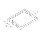
図1は、本発明の実施形態に係る液晶表示装置100のモールド部110を示した斜視図である。 FIG. 1 is a perspective view showing a
図1に示すように、上記モールド部110は、液晶表示装置が形成されるための基本的なフレームになるものである。上記モールド部110は、モールドフレーム111、上記モールドフレーム111が形成されない領域の開放部112、上記モールドフレーム111の一面に形成された結合溝113及び上記結合溝113の上部(液晶表示側の部位)に形成された曲面114を含むことができる。 As shown in FIG. 1, the
上記モールドフレーム111は、上記モールド部110の端部分に一定な高さを保持して形成される。上記モールドフレーム111は、液晶表示パネルの上部にウィンドウ(window)が形成される場合、上記ウィンドウを支持するために形成される。よって、上記モールドフレーム111の高さは一定である。 The
上記開放部112は、上記モールドフレーム111が形成されない領域を意味する。上記開放部112は、外部に開口し、後にフレキシブルプリント回路が外部の印刷回路基板(PCB)と連結されるための通路を提供する。フレキシブルプリント回路は、外部の印刷回路基板(PCB)とバックライトユニット(BLU)、高密度集積回路を相互に連結する役割を有する。よって、上記フレキシブルプリント回路が外部の印刷回路基板(PCB)に連結されるためには、上記モールド部110の部分のうち、端にモールドフレーム111が形成されない領域が要され、この部分が開放部112になる。 The
図1に示すように、上記結合溝113は、上記モールドフレーム111の一面に形成される。より詳しくは、上記結合溝113は、上記開放部112と接するモールドフレーム111の内部に形成される。また、図1に示すように、上記結合溝113は上記モールドフレーム111の内部に直方体(六面体)の形状に陰刻されている。 As shown in FIG. 1, the
上記結合溝113は、後にフレキシブルプリント回路が結合される部分である。上述のようにフレキシブルプリント回路は、上記モールド部110の背面に回して組み立てられる構造が多く、フレキシブルプリント回路の復元力が作用する。 The
従来の場合、上記復元力でフレキシブルプリント回路の浮き問題が発生した。しかし、本発明の実施形態に係る液晶表示装置100では、上記結合溝113が形成されてフレキシブルプリント回路を固定する役割を有する。よって、上記フレキシブルプリント回路の浮き問題が防止される。 In the conventional case, a floating problem of the flexible printed circuit occurs due to the restoring force. However, in the liquid
上記曲面114は、上記モールドフレーム111のうち上記結合溝113の上面(液晶表示側の面)に形成される。上記曲面114は、四分円形状である。上記曲面114が形成される理由は、製造工程において、上記フレキシブルプリント回路が上記結合溝113に結合されることを容易にするためである。製造工程時に上記フレキシブルプリント回路が上記モールドフレーム111にかかって結合溝113に結合できない虞がある。よって、上記曲面114を上記モールドフレーム111に形成し、フレキシブルプリント回路が上記曲面114にかかる場合でも、上記曲面114に沿って移動して上記結合溝113に結合することを容易にする。 The
上述のように本発明の実施形態に係る液晶表示装置100は、結合溝113を備えたモールド部110を含む。よって、上記結合溝113にフレキシブルプリント回路が結合して固定されることで、フレキシブルプリント回路の復元力による浮きを防止する。また、上記曲面114を上記結合溝113の上部に形成しているため、上記フレキシブルプリント回路を上記結合溝113に容易に結合することができる。 As described above, the liquid
以下、本発明に係る液晶表示装置100の製造される手順を説明する。 Hereinafter, a procedure for manufacturing the liquid
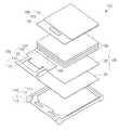
図2に示すように、本発明に係る液晶表示装置100が製造される手順を説明するための分解斜視図が示されている。 As shown in FIG. 2, an exploded perspective view for explaining a procedure for manufacturing the liquid
図2に示すように、本発明に係る液晶表示装置100は、モールド部110、上記モールド部110の上面に形成されるパネル下部層120、上記パネル下部層120の一側面に形成されるフレキシブルプリント回路130、上記フレキシブルプリント回路130の背面に形成されるバックライトユニット140及び上記パネル下部層120の上面に形成される液晶表示パネル150を含むことができる。 As shown in FIG. 2, the liquid
尚、実施形態を説明するための全図において、同一機能を有するものには同一符号を付し、以下ではその差を中心に説明する。 In all the drawings for explaining the embodiments, the same reference numerals are given to those having the same function, and the difference will be mainly described below.
上記モールド部110は、モールドフレーム111、開放部112、結合溝113、及び曲面114を含む。上述のように上記フレキシブルプリント回路130は、上記結合溝113に結合されて固定されるので、フレキシブルプリント回路130の浮き問題が防止され、上記曲面114を介して上記フレキシブルプリント回路130が結合溝113に結合することが容易になる。上記モールド部110の説明は、上述と同様であるため、以下の説明は省略する。 The
上記パネル下部層120は、反射板121、上記反射板121の上部に形成される導光板122、及び上記導光板122の上部に形成される光学シート123を含むことができる。 The panel
上記反射板121は、上記モールド部110の上面に形成される。上記反射板121は、上記バックライトユニット140から入射された光を反射して上記液晶表示パネル150の方向に入射させる役割を有する。上記反射板121は、主にポリエステル(PFT)基材あるいは上記導光板122に入射された光源の損失低減のために光反射機能を有する。 The
上記導光板122は、上記反射板121の上部に形成される。上記導光板122は、主にアクリル(PMMA)で構成され、入射された光源を導光して構成されたパターンは、光源を均一に分布させる。上記導光板122は、射出成形法(Injection molding method)またはキャスティング法(casting method)で製作される。 The
上記光学シート123は、上記導光板122の上部に形成され、二枚の拡散シート、拡散シートの間に形成される二枚のプリズムシートを含むことができる。 The
上記拡散シートは、主にポリエステル(PFT)機材にアクリル係の樹脂を利用して製作され、円形状に形成させて上記導光板122から出光された光源を均一に分布させると同時に、光を集光する役割も有する。上記拡散シートは、上記プリズムシートを保護する役割を主目的とするので、保護フィルムともいう。 The diffusion sheet is mainly made of polyester (PFT) equipment using an acrylic resin, and is formed into a circular shape to uniformly distribute the light source emitted from the
上記プリズムシートは、主にポリエステル(PFT)基材にアクリル係の樹脂を利用し、プリズム形状を規則的に形成させて光を集光する役割を有する。 The prism sheet mainly has a role of condensing light by regularly forming a prism shape using an acrylic resin on a polyester (PFT) base material.
上記フレキシブルプリント回路130は、上記光学シート123の一面に形成される。詳しくは、上記フレキシブルプリント回路130は、上記光学シート123の上面のうち上記モールド部110の開放部112に相応する部分に形成される。上記フレキシブルプリント回路130が開放部112に該当する部分に形成されることで、上記開放部112を介して上記フレキシブルプリント回路130が外部の印刷回路基板(PCB)と結合できることは、上述の通りである。 The flexible printed
上記フレキシブルプリント回路130は、図2に示すように、平坦部131、上記平坦部131の端に形成されるエッジ部132、上記平坦部131の一面に形成されているパネル連結部133、上記平坦部131と連結されている屈曲部134、上記屈曲部に連結されている外部連結部135とを含むことができる。 2, the flexible printed
上記平坦部131は、図2に示すように、上記光学シート123と連結されて繋がれる領域である。上記平坦部131は、上記光学シート123と連結され、上記導光板122が備えられたモールド部110の上面に形成される。また、上記平坦部131は、後に上記液晶表示パネル150によって押さえられるようになるので、全般的に上記フレキシブルプリント回路130を支持する役割を有する。 As shown in FIG. 2, the
上記エッジ部132は、上記平坦部131の端に形成される。詳しくは、上記エッジ部132は、上記平坦部132が上記屈曲部134と連結された部分の端の領域を意味する。上記フレキシブルプリント回路130が上記結合溝113と結合する場合、上記エッジ部132が上記結合溝113と結合する部分になる。 The
上記エッジ部132が上記結合溝113に結合すると、上記フレキシブルプリント回路130が復元力を受けることによる浮きの発生を防止できることは、上述の通りである。 As described above, when the
上記パネル連結部133は、図2に示すように、上記平坦部131の一面に形成されている。上記パネル連結部133は、フレキシブルがあって、上記フレキシブルプリント回路130の上部に形成された液晶表示パネル150の方向に曲がる。より詳しくは、上記パネル連結部133は、上記液晶表示パネル150の高密度集積回路153と電気的に接続されるために上面に曲がる。 The
上記屈曲部134は、上記フレキシブルプリント回路130が外部の印刷回路基板(PCB)に連結されるために上記モールド部110の背面に曲がる部分である。すなわち、上記平坦部131及びエッジ部132は、上記光学シート123に付着して固定され、上記屈曲部134が上記モールド部110の背面に曲がって外部の印刷回路基板(PCB)に接続される。 The
この場合、上記屈曲部134は、上記液晶表示パネル150に向かう方向に復元力を受ける。従来、このような場合に復元力によってフレキシブルプリント回路の浮きが発生する問題があり、追加的に、その上面に形成された液晶表示パネルの浮きおよび信頼性にも問題があった。 In this case, the
しかし、本発明の実施形態に係る液晶表示装置100において、上述のように上記フレキシブルプリント回路130のエッジ部132が上記モールド部110の結合溝113に結合する。これにより、上述した屈曲部134の復元力にもかかわらず、上記のようなフレキシブルプリント回路の浮きや液晶表示パネル浮きなどの問題が発生しない。 However, in the liquid
上記外部連結部135は、上記屈曲部134に連結される。上記屈曲部134がモールド部110の背面に曲がる場合、上記外部連結部135が外部の印刷回路基板(PCB)と電気的に接続される。 The
上記バックライトユニット140は、図2に示すように、上記フレキシブルプリント回路130の背面に形成される。よって、上記フレキシブルプリント回路130が上記モールド部110に組み立てられる場合、上記バックライトユニット140は、上記モールド部110の方向に向けるように上記導光板122と反射板121に光を提供する。上記バックライトユニット140は、高電圧が印加されて可視光線を発生する光源として、冷陰極蛍光ランプ(CCFL:Cold Cathod Flourescent Lamp)または高輝度発光ダイオードが主に用いられる。 The
上記液晶表示パネル150は、上記光学シート123の上面に形成される。上記液晶表示パネル150は、一般的にブラックマトリックス及びカラーフィルターを備える上部基板151と、薄膜トランジスタを備える下部基板152と、上記上部基板151と下部基板152との間に注入された液晶を含む。 The liquid
また、図2に示すように、上記下部基板152の上面には高密度集積回路153が形成される。 Further, as shown in FIG. 2, a high density
上記高密度集積回路153は、上記バックライトユニット140と液晶表示パネル150を駆動するために、上記フレキシブルプリント回路130を介して上記バックライトユニット140に電気的に接続される。また、上記フレキシブルプリント回路130を介して外部の印刷回路基板(PCB)と電気的に接続される。よって、上記高密度集積回路153は、外部の印刷回路基板(PCB)から電気的な信号が印加されて上記バックライトユニット140が発光するようにし、上記液晶表示パネル150の液晶を配列させて映像を表示する。 The high-density
以下、本発明の実施形態に係る液晶表示装置100において、モールド部110にフレキシブルプリント回路130が結合される過程を説明する。 Hereinafter, a process in which the flexible printed
図3は、本発明の実施形態に係る液晶表示装置100のモールド部110にフレキシブルプリント回路130が結合される過程を説明するための斜視図である。 FIG. 3 is a perspective view illustrating a process in which the flexible printed
図3に示すように、上記モールド部110の結合溝113に上記フレキシブルプリント回路130のエッジ部132が結合される。すなわち、従来の技術と異なり、上記フレキシブルプリント回路130のエッジ部132が上記モールド部110の結合溝113に挿入される構造である。 As shown in FIG. 3, the
また、上記フレキシブルプリント回路130が上記モールド部110に結合される場合、上記モールド部110の曲面114の結合が容易になる。すなわち、製造工程において、上記エッジ部132が上記結合溝113に正確に結合されない場合、上記結合溝113の方向に力を加えれば、上記エッジ部132は上記曲面114に沿って移動するようになり、結局、上記結合溝113に結合される。すなわち、製造工程での不良率を低減させる。 In addition, when the flexible printed
以下、本発明の実施形態に係る液晶表示装置100でフレキシブルプリント回路が曲がる場合を説明する。 Hereinafter, a case where the flexible printed circuit is bent in the liquid
図4は、本発明の実施形態に係る液晶表示装置100でフレキシブルプリント回路130が曲がることを示した斜視図である。 FIG. 4 is a perspective view showing that the flexible printed
図4に示すように、上記エッジ部132が上記結合溝113に結合されている。よって、上記フレキシブルプリント回路130の屈曲部134が曲がる場合に生ずる復元力を、上記結合溝113を備えるモールドフレーム111が防止させる。つまり、上述した従来のフレキシブルプリント回路の浮き、液晶表示パネルの浮きの問題が防止される。 As shown in FIG. 4, the
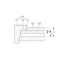
以下、本発明の実施形態に係る液晶表示装置100において、モールド部110にフレキシブルプリント回路130が結合された構造を、断面図を参照して説明する。 Hereinafter, in the liquid
図5は、本発明の実施形態に係る液晶表示装置100のモールド部110にフレキシブルプリント回路130が結合されたことを示した断面図である。 FIG. 5 is a cross-sectional view showing that the flexible printed
図5に示すように、上記モールド部110の結合溝113に上記フレキシブルプリント回路130のエッジ部132が結合され、上記フレキシブルプリント回路130の上面には上記液晶表示パネル150の下部基板152が形成されている。なお、図5は、本発明の実施形態を説明するためのものであり、表示される各部分の実際の割合とは異なることができる。 As shown in FIG. 5, the
図5に示すように、上記エッジ部132が上記結合溝113に挿入されることで、上記結合溝113が形成されたモールドフレーム111が、フレキシブルプリント回路130の復元力を妨げるようになる。 As shown in FIG. 5, when the
また、図5に示すように、上記結合溝113の厚さ(b)は、少なくとも上記エッジ部132の厚さ(a)よりは厚くなければならない。これは、上記結合溝113に上記エッジ部132を結合可能にさせるためである。また、上記結合溝113と曲面114を合わせた厚さ(c)は、上記結合溝113の厚さ(b)より厚くなければならないことが分かる。 Further, as shown in FIG. 5, the thickness (b) of the
以下、本発明の実施形態に係る液晶表示装置100の製造方法について説明する。 Hereinafter, a manufacturing method of the liquid
図2に示すように、本発明の実施形態に係る液晶表示装置100は、モールド部110を備えるモールド部具備段階、上記モールド部110の上面にパネル下部層120が形成されるパネル下部層形成段階、上記パネル下部層120にフレキシブルプリント回路130が形成されるフレキシブルプリント回路形成段階、上記パネル下部層120の上部に液晶表示パネル150が形成される液晶表示パネル形成段階とを含むことができる。 As shown in FIG. 2, the liquid
上記モールド部具備段階は、本発明の実施形態に係る液晶表示装置100のフレームになるモールド部110を備える段階である。上記モールド部具備段階は、鋼材(SUS)のベゼルを備え、上記ベゼルに合成樹脂に成形されたモールドフレーム111及び開放部112が形成される段階を含む。上記ベゼルは、プレスによって鋼材(SUS)のシートが折曲成形されて製造され、上記モールドフレーム111及び開放部112はポリカーボネート(PC)などの合成樹脂が成形されて製造される。上記ベゼルには、複数の締結孔が形成され、モールドフレーム111にはフック(hook)が形成され、上記締結孔とフックの結合に組み立てられる。 The step of providing the mold unit is a step of providing a
上記モールド部具備段階の上記モールドフレーム111は、結合溝113を備えることができる。上記フレキシブルプリント回路130のエッジ部132が上記結合溝113に結合されて従来のフレキシブルプリント回路の浮きなどの問題が解決できることは、上述の通りである。 The
また、上記モールド部具備段階のモールドフレーム111は、曲面114を備えることができる。上記エッジ部132が結合溝113に正確に結合されない場合でも、上記エッジ部132が上記曲面114に沿って移動して上記結合溝113に結合できることは、上述の通りである。 In addition, the
上記パネル下部層形成段階は、上記モールド部110の上面に上記パネル下部層120を形成する段階である。上記パネル下部層120は、上述のように反射板121、導光板122、及び光学シート123を含んで構成される。上記パネル下部層形成段階では、上記反射板121、導光板122、光学シート123の順に上記モールド部110の上面に形成される。 The panel lower layer forming step is a step of forming the panel
上記フレキシブルプリント回路形成段階は、上記光学シート123の一側面にフレキシブルプリント回路130を形成する段階である。上記フレキシブルプリント回路130は、上述のように平坦部131、上記平坦部の一側面に形成されたエッジ部132、上記平坦部131に連結されたパネル連結部133、上記平坦部131に連結された屈曲部134、及び上記屈曲部に連結された外部連結部135を含んで構成される。また、上記平坦部131の背面には、上記バックライトユニット140が形成できることは、上述の通りである。 The flexible printed circuit forming step is a step of forming the flexible printed
上記液晶表示パネル形成段階は、上記パネル下部層120の上面に上記液晶表示パネル150が形成される段階である。上記液晶表示パネル150は、ブラックマトリックス及びカラーフィルターが形成された上部基板151、薄膜トランジスタが形成された下部基板152、上記下部基板153の上部に形成される高密度集積回路153などを含むことができることは上述の通りである。また、別途に示してないが、上記上部基板151と下部基板152との間に液晶が注入されることは勿論であり、説明は省略する。 The liquid crystal display panel forming step is a step in which the liquid
上記のように本発明の実施形態に係る液晶表示装置100が製造される。また、上記の段階後に上記フレキシブルプリント回路130のパネル連結部133及び外部連結部135は、それぞれ上記高密度集積回路153、外部の印刷回路基板(PCB)に連結される。 As described above, the liquid
以上、本発明は、上述した特定の好適な実施形態に限定されるものではなく、特許請求の範囲に記載された本発明の技術的思想に基づき、当該技術分野における通常の知識を有する者であれば、様々な実施変形が可能であり、そのような変形は本発明の技術的範囲に属するものである。 As described above, the present invention is not limited to the specific preferred embodiment described above, and is based on the technical idea of the present invention described in the claims, and has a general knowledge in the technical field. If it exists, various implementation deformation | transformation are possible, and such a deformation | transformation belongs to the technical scope of this invention.
100 液晶表示装置、
110 モールド部、
111 モールドフレーム、
112 開放部、
113 結合溝、
114 曲面、
120 パネル下部層、
121 反射板、
122 導光板、
123 光学シート、
130 フレキシブルプリント回路、
131 平坦部、
132 エッジ部、
133 パネル連結部、
134 屈曲部、
135 外部連結部、
140 バックライトユニット、
150 液晶表示パネル、
151 上部基板、
152 下部基板、
153 高密度集的回路。100 liquid crystal display device,
110 Mold part,
111 mold frame,
112 opening part,
113 coupling groove,
114 curved surface,
120 Panel lower layer,
121 reflector,
122 light guide plate,
123 optical sheet,
130 flexible printed circuit,
131 flat part,
132 edge part,
133 Panel connection part,
134 bends,
135 External connection,
140 backlight unit,
150 liquid crystal display panel,
151 Upper substrate,
152 lower substrate,
153 High density integrated circuit.
Claims (16)
Translated fromJapanese前記モールド部の液晶表示側である上部に形成される光学シートと、
前記光学シートの一側面に形成される軟性印刷回路と、を含み、
前記モールド部は、
ウィンドウを支持するモールドフレームと、
前記モールドフレームが形成されずに開口する開放部と、を含み、
前記モールド部の一面には前記軟性印刷回路が固定して結合される結合溝が形成され、
前記モールドフレームは、前記結合溝の液晶表示側である上面に曲面を備え、
前記軟性印刷回路は、結合時に平面が曲がらない、前記光学シートに結合される発光ダイオードを持つ平坦部と、
前記平坦部に形成されるエッジ部と、
前記平坦部に連結され、結合時に曲がる屈曲部と、を含み、
前記エッジ部は前記結合溝に結合されることを特徴とする液晶表示装置。Mold part,
An optical sheet formed on the liquid crystal display side of the mold part;
A flexible printed circuit formed on one side of the optical sheet,
The mold partis
A mold frame that supports the window;
An opening that opens without forming the mold frame,
A coupling groove is formed on one surface of the mold portion to which the flexible printed circuit is fixed and coupled,
The mold frame has a curved surface on the upper surface on the liquid crystal display side of the coupling groove,
The flexible printed circuit has a flat portion having a light emitting diode coupled to the optical sheet, the plane does not bend when coupled;
An edge portion formed on the flat portion;
A bent portion connected to the flat portion and bent at the time of coupling,
The liquid crystal display device,wherein the edge portion is coupled to the coupling groove .
前記モールド部の液晶表示側である上部に光学シートを形成するパネル下部層形成段階と、
前記光学シートの一側面に軟性印刷回路を形成する軟性印刷回路形成段階と、を含み、
前記モールド部の一面には前記軟性印刷回路が固定して結合されるようにする結合溝が形成され、前記モールド部具備段階の前記モールドフレームは、前記結合溝の液晶表示側である上面に曲面を備え、
前記軟性印刷回路は、結合時に平面が曲がらない、前記光学シートに結合される発光ダイオードを持つ平坦部と、
前記平坦部に形成されるエッジ部と、
前記平坦部に連結され、結合時に曲がる屈曲部と、を含み、
前記エッジ部は前記結合溝に結合されることを特徴とする液晶表示装置の製造方法。A mold partcomprising a mold part thatincludes a mold frame that supports a window and an open part that is opened without forming the mold frame; and
A panel lower layer forming step of forming an optical sheet on the liquid crystal display side of the mold part;
Forming a soft printed circuit on one side of the optical sheet,
A coupling groove for fixing and coupling the flexible printed circuit is formed onone surface of the mold part, andthemold frame at the stage of providing the mold part has a curved surface on an upper surface on the liquid crystal display side of the coupling groove. With
The flexible printed circuit has a flat portion having a light emitting diode coupled to the optical sheet, the plane does not bend when coupled;
An edge portion formed on the flat portion;
A bent portion connected to the flat portion and bent at the time of coupling,
The method for manufacturing a liquid crystal display device,wherein the edge portion is coupled to the coupling groove .
Applications Claiming Priority (2)
| Application Number | Priority Date | Filing Date | Title |
|---|---|---|---|
| KR10-2007-0066199 | 2007-07-02 | ||
| KR1020070066199AKR100876248B1 (en) | 2007-07-02 | 2007-07-02 | Liquid Crystal Display and Manufacturing Method Thereof |
Publications (2)
| Publication Number | Publication Date |
|---|---|
| JP2009015321A JP2009015321A (en) | 2009-01-22 |
| JP4920641B2true JP4920641B2 (en) | 2012-04-18 |
Family
ID=39722005
Family Applications (1)
| Application Number | Title | Priority Date | Filing Date |
|---|---|---|---|
| JP2008162454AExpired - Fee RelatedJP4920641B2 (en) | 2007-07-02 | 2008-06-20 | Liquid crystal display device and manufacturing method thereof |
Country Status (6)
| Country | Link |
|---|---|
| US (1) | US7894013B2 (en) |
| EP (1) | EP2012567B1 (en) |
| JP (1) | JP4920641B2 (en) |
| KR (1) | KR100876248B1 (en) |
| CN (1) | CN101339304B (en) |
| DE (1) | DE602008001210D1 (en) |
Families Citing this family (20)
| Publication number | Priority date | Publication date | Assignee | Title |
|---|---|---|---|---|
| KR101415968B1 (en)* | 2007-11-06 | 2014-07-08 | 엘지디스플레이 주식회사 | Backlight unit for liquid crystal display device and liquid crystal display device module |
| KR101345172B1 (en)* | 2008-07-18 | 2013-12-27 | 엘지디스플레이 주식회사 | Electrophoretic display deivce |
| US20100228090A1 (en)* | 2009-03-06 | 2010-09-09 | Ethicon Endo-Surgery, Inc. | Methods and devices for providing access into a body cavity |
| KR101055021B1 (en) | 2010-04-01 | 2011-08-05 | 엘지이노텍 주식회사 | Backlight Unit and Display Device |
| US9453959B2 (en) | 2010-03-30 | 2016-09-27 | Lg Innotek Co., Ltd. | Backlight unit and display apparatus |
| KR101661477B1 (en)* | 2010-04-27 | 2016-10-04 | 삼성디스플레이 주식회사 | Liquid crystal display device |
| US20120320627A1 (en) | 2011-05-17 | 2012-12-20 | Pixi Lighting Llc | Flat panel lighting device and driving circuitry |
| JP5663434B2 (en) | 2011-08-15 | 2015-02-04 | 株式会社ジャパンディスプレイ | Display device |
| KR101861628B1 (en) | 2011-09-16 | 2018-05-29 | 삼성디스플레이 주식회사 | Liquid crystal display device |
| JP2016508624A (en) | 2013-02-20 | 2016-03-22 | エルジー・ケム・リミテッド | Packaging film for display devices |
| US9500328B2 (en) | 2013-04-17 | 2016-11-22 | Pixi Lighting, Inc. | Lighting assembly |
| US9476552B2 (en) | 2013-04-17 | 2016-10-25 | Pixi Lighting, Inc. | LED light fixture and assembly method therefor |
| US9546781B2 (en) | 2013-04-17 | 2017-01-17 | Ever Venture Solutions, Inc. | Field-serviceable flat panel lighting device |
| KR102018741B1 (en) | 2013-06-03 | 2019-09-06 | 삼성디스플레이 주식회사 | Display device with cover window |
| KR102263821B1 (en)* | 2013-12-09 | 2021-06-14 | 삼성디스플레이 주식회사 | Display apparatus |
| US20160174398A1 (en)* | 2014-12-16 | 2016-06-16 | Kabushiki Kaisha Toshiba | Electronic apparatus |
| US9557022B2 (en) | 2015-04-30 | 2017-01-31 | Ever Venture Solutions, Inc. | Non-round retrofit recessed LED lighting fixture |
| CN107393948B (en)* | 2017-08-11 | 2020-05-19 | 武汉华星光电半导体显示技术有限公司 | Middle frame and flexible display device for fixing flexible display panel |
| CN110082961B (en)* | 2019-05-27 | 2024-04-05 | 武汉华星光电技术有限公司 | Glue frame, backlight module and display device |
| KR102624015B1 (en)* | 2019-07-10 | 2024-01-11 | 삼성디스플레이 주식회사 | Display device |
Family Cites Families (13)
| Publication number | Priority date | Publication date | Assignee | Title |
|---|---|---|---|---|
| JP2002142331A (en)* | 2000-10-31 | 2002-05-17 | Yazaki Corp | Flexible circuit take-out structure |
| JP3976722B2 (en)* | 2003-10-20 | 2007-09-19 | 埼玉日本電気株式会社 | Connection structure between functional panel and circuit board via flexible wiring board and electronic device |
| TWI231740B (en)* | 2004-05-20 | 2005-04-21 | Au Optronics Corp | Display module and locating method of flexible print circuit board thereof |
| JP4196888B2 (en)* | 2004-06-25 | 2008-12-17 | セイコーエプソン株式会社 | Electro-optical device and electronic apparatus |
| TWM263518U (en)* | 2004-07-06 | 2005-05-01 | Au Optronics Corp | Backlight module |
| KR101122216B1 (en)* | 2004-11-29 | 2012-03-19 | 삼성전자주식회사 | Backlight assembly and display apparatus having the same |
| KR101171178B1 (en)* | 2005-01-04 | 2012-08-06 | 삼성전자주식회사 | An original plate for a flexible printed circuit board formed with a cutting pattern and a flat display device provided with a cutted flexible printed circuit board from the same |
| TWM276149U (en)* | 2005-04-15 | 2005-09-21 | Innolux Display Corp | Back light module |
| KR20060128249A (en) | 2005-06-10 | 2006-12-14 | 삼성전자주식회사 | Driving module connecting device, liquid crystal display device having same and fastening method thereof |
| KR20070011751A (en) | 2005-07-21 | 2007-01-25 | 삼성전자주식회사 | Chassis of liquid crystal display and liquid crystal display including the same |
| KR20070054353A (en) | 2005-11-23 | 2007-05-29 | 삼성전자주식회사 | Display device |
| TW200815870A (en)* | 2006-09-29 | 2008-04-01 | Innolux Display Corp | Backlight unit and liquid crystal display device |
| KR100869675B1 (en) | 2007-02-05 | 2008-11-21 | 지인정보기술 주식회사 | Flash memory control system and method using descriptor array |
- 2007
- 2007-07-02KRKR1020070066199Apatent/KR100876248B1/ennot_activeExpired - Fee Related
- 2008
- 2008-06-20JPJP2008162454Apatent/JP4920641B2/ennot_activeExpired - Fee Related
- 2008-06-30USUS12/165,265patent/US7894013B2/enactiveActive
- 2008-07-01DEDE602008001210Tpatent/DE602008001210D1/enactiveActive
- 2008-07-01EPEP08159405Apatent/EP2012567B1/ennot_activeCeased
- 2008-07-02CNCN2008101260640Apatent/CN101339304B/ennot_activeExpired - Fee Related
Also Published As
| Publication number | Publication date |
|---|---|
| CN101339304B (en) | 2010-11-10 |
| US20090009682A1 (en) | 2009-01-08 |
| CN101339304A (en) | 2009-01-07 |
| KR100876248B1 (en) | 2008-12-26 |
| DE602008001210D1 (en) | 2010-06-24 |
| US7894013B2 (en) | 2011-02-22 |
| EP2012567B1 (en) | 2010-05-12 |
| EP2012567A1 (en) | 2009-01-07 |
| JP2009015321A (en) | 2009-01-22 |
Similar Documents
| Publication | Publication Date | Title |
|---|---|---|
| JP4920641B2 (en) | Liquid crystal display device and manufacturing method thereof | |
| CN101183200B (en) | Liquid crystal display device | |
| CN100428013C (en) | Liquid crystal display device having a plurality of pixel electrodes | |
| KR101177909B1 (en) | Backlight assembly for Liquid Crystal display and Liquid Crystal Module using thereof | |
| EP2192438B1 (en) | Liquid crystal display module | |
| KR101244775B1 (en) | Liquid crystal display module | |
| KR20080001751A (en) | LCD Display | |
| US20070086213A1 (en) | Backlight module with interengaging frame and light guide plate and liquid crystal display device with same | |
| CN102102831A (en) | Backlight unit and liquid crystal display device having the same | |
| CN203686916U (en) | Rubber frame, backlight module and display device | |
| CN204807879U (en) | Lamp strip fixed adhesive tape , backlight unit and display device | |
| JP5312919B2 (en) | Liquid crystal display | |
| CN110908191A (en) | Display module and display device | |
| CN116540441A (en) | Display module, manufacturing method thereof and display device | |
| KR102001855B1 (en) | Liquid crystal display device | |
| JP5638371B2 (en) | Planar light source device and display device | |
| KR101260015B1 (en) | Backlight assembly and liquid crystal display comprising the same | |
| JP2007304306A (en) | Fixing structure of liquid crystal display panel | |
| US20090186661A1 (en) | Display device | |
| KR20080013311A (en) | Liquid crystal display | |
| EP2372418B1 (en) | Backlight unit and display apparatus | |
| CN114624808A (en) | Backlight module and display device | |
| JP2005250269A (en) | Backlight structure for liquid crystal display device | |
| KR20200130598A (en) | Display apparatus having optical distance | |
| JP4289992B2 (en) | Liquid crystal display |
Legal Events
| Date | Code | Title | Description |
|---|---|---|---|
| A711 | Notification of change in applicant | Free format text:JAPANESE INTERMEDIATE CODE: A712 Effective date:20081201 | |
| A131 | Notification of reasons for refusal | Free format text:JAPANESE INTERMEDIATE CODE: A131 Effective date:20110405 | |
| A601 | Written request for extension of time | Free format text:JAPANESE INTERMEDIATE CODE: A601 Effective date:20110629 | |
| A602 | Written permission of extension of time | Free format text:JAPANESE INTERMEDIATE CODE: A602 Effective date:20110708 | |
| A521 | Written amendment | Free format text:JAPANESE INTERMEDIATE CODE: A523 Effective date:20110729 | |
| TRDD | Decision of grant or rejection written | ||
| A01 | Written decision to grant a patent or to grant a registration (utility model) | Free format text:JAPANESE INTERMEDIATE CODE: A01 Effective date:20120124 | |
| A01 | Written decision to grant a patent or to grant a registration (utility model) | Free format text:JAPANESE INTERMEDIATE CODE: A01 | |
| A61 | First payment of annual fees (during grant procedure) | Free format text:JAPANESE INTERMEDIATE CODE: A61 Effective date:20120201 | |
| R150 | Certificate of patent or registration of utility model | Ref document number:4920641 Country of ref document:JP Free format text:JAPANESE INTERMEDIATE CODE: R150 Free format text:JAPANESE INTERMEDIATE CODE: R150 | |
| FPAY | Renewal fee payment (event date is renewal date of database) | Free format text:PAYMENT UNTIL: 20150210 Year of fee payment:3 | |
| FPAY | Renewal fee payment (event date is renewal date of database) | Free format text:PAYMENT UNTIL: 20150210 Year of fee payment:3 | |
| S111 | Request for change of ownership or part of ownership | Free format text:JAPANESE INTERMEDIATE CODE: R313111 | |
| FPAY | Renewal fee payment (event date is renewal date of database) | Free format text:PAYMENT UNTIL: 20150210 Year of fee payment:3 | |
| R371 | Transfer withdrawn | Free format text:JAPANESE INTERMEDIATE CODE: R371 | |
| S111 | Request for change of ownership or part of ownership | Free format text:JAPANESE INTERMEDIATE CODE: R313111 | |
| FPAY | Renewal fee payment (event date is renewal date of database) | Free format text:PAYMENT UNTIL: 20150210 Year of fee payment:3 | |
| R350 | Written notification of registration of transfer | Free format text:JAPANESE INTERMEDIATE CODE: R350 | |
| R250 | Receipt of annual fees | Free format text:JAPANESE INTERMEDIATE CODE: R250 | |
| R250 | Receipt of annual fees | Free format text:JAPANESE INTERMEDIATE CODE: R250 | |
| R250 | Receipt of annual fees | Free format text:JAPANESE INTERMEDIATE CODE: R250 | |
| R250 | Receipt of annual fees | Free format text:JAPANESE INTERMEDIATE CODE: R250 | |
| R250 | Receipt of annual fees | Free format text:JAPANESE INTERMEDIATE CODE: R250 | |
| R250 | Receipt of annual fees | Free format text:JAPANESE INTERMEDIATE CODE: R250 | |
| LAPS | Cancellation because of no payment of annual fees |