JP4914530B1 - Terminal device - Google Patents
Terminal deviceDownload PDFInfo
- Publication number
- JP4914530B1 JP4914530B1JP2011194187AJP2011194187AJP4914530B1JP 4914530 B1JP4914530 B1JP 4914530B1JP 2011194187 AJP2011194187 AJP 2011194187AJP 2011194187 AJP2011194187 AJP 2011194187AJP 4914530 B1JP4914530 B1JP 4914530B1
- Authority
- JP
- Japan
- Prior art keywords
- substrate
- electronic component
- rubber member
- terminal device
- electrically connected
- Prior art date
- Legal status (The legal status is an assumption and is not a legal conclusion. Google has not performed a legal analysis and makes no representation as to the accuracy of the status listed.)
- Active
Links
Images


Classifications
- H—ELECTRICITY
- H05—ELECTRIC TECHNIQUES NOT OTHERWISE PROVIDED FOR
- H05K—PRINTED CIRCUITS; CASINGS OR CONSTRUCTIONAL DETAILS OF ELECTRIC APPARATUS; MANUFACTURE OF ASSEMBLAGES OF ELECTRICAL COMPONENTS
- H05K1/00—Printed circuits
- H05K1/02—Details
- H05K1/0275—Security details, e.g. tampering prevention or detection
- G—PHYSICS
- G06—COMPUTING OR CALCULATING; COUNTING
- G06F—ELECTRIC DIGITAL DATA PROCESSING
- G06F21/00—Security arrangements for protecting computers, components thereof, programs or data against unauthorised activity
- G06F21/70—Protecting specific internal or peripheral components, in which the protection of a component leads to protection of the entire computer
- G06F21/86—Secure or tamper-resistant housings
- H—ELECTRICITY
- H05—ELECTRIC TECHNIQUES NOT OTHERWISE PROVIDED FOR
- H05K—PRINTED CIRCUITS; CASINGS OR CONSTRUCTIONAL DETAILS OF ELECTRIC APPARATUS; MANUFACTURE OF ASSEMBLAGES OF ELECTRICAL COMPONENTS
- H05K1/00—Printed circuits
- H05K1/02—Details
- H05K1/0213—Electrical arrangements not otherwise provided for
- H—ELECTRICITY
- H05—ELECTRIC TECHNIQUES NOT OTHERWISE PROVIDED FOR
- H05K—PRINTED CIRCUITS; CASINGS OR CONSTRUCTIONAL DETAILS OF ELECTRIC APPARATUS; MANUFACTURE OF ASSEMBLAGES OF ELECTRICAL COMPONENTS
- H05K5/00—Casings, cabinets or drawers for electric apparatus
- H05K5/02—Details
- H05K5/0208—Interlock mechanisms; Means for avoiding unauthorised use or function, e.g. tamperproof
- H—ELECTRICITY
- H05—ELECTRIC TECHNIQUES NOT OTHERWISE PROVIDED FOR
- H05K—PRINTED CIRCUITS; CASINGS OR CONSTRUCTIONAL DETAILS OF ELECTRIC APPARATUS; MANUFACTURE OF ASSEMBLAGES OF ELECTRICAL COMPONENTS
- H05K1/00—Printed circuits
- H05K1/02—Details
- H05K1/14—Structural association of two or more printed circuits
- H05K1/141—One or more single auxiliary printed circuits mounted on a main printed circuit, e.g. modules, adapters
- H—ELECTRICITY
- H05—ELECTRIC TECHNIQUES NOT OTHERWISE PROVIDED FOR
- H05K—PRINTED CIRCUITS; CASINGS OR CONSTRUCTIONAL DETAILS OF ELECTRIC APPARATUS; MANUFACTURE OF ASSEMBLAGES OF ELECTRICAL COMPONENTS
- H05K1/00—Printed circuits
- H05K1/02—Details
- H05K1/14—Structural association of two or more printed circuits
- H05K1/147—Structural association of two or more printed circuits at least one of the printed circuits being bent or folded, e.g. by using a flexible printed circuit
- H—ELECTRICITY
- H05—ELECTRIC TECHNIQUES NOT OTHERWISE PROVIDED FOR
- H05K—PRINTED CIRCUITS; CASINGS OR CONSTRUCTIONAL DETAILS OF ELECTRIC APPARATUS; MANUFACTURE OF ASSEMBLAGES OF ELECTRICAL COMPONENTS
- H05K2201/00—Indexing scheme relating to printed circuits covered by H05K1/00
- H05K2201/03—Conductive materials
- H05K2201/0302—Properties and characteristics in general
- H05K2201/0314—Elastomeric connector or conductor, e.g. rubber with metallic filler
- H—ELECTRICITY
- H05—ELECTRIC TECHNIQUES NOT OTHERWISE PROVIDED FOR
- H05K—PRINTED CIRCUITS; CASINGS OR CONSTRUCTIONAL DETAILS OF ELECTRIC APPARATUS; MANUFACTURE OF ASSEMBLAGES OF ELECTRICAL COMPONENTS
- H05K2201/00—Indexing scheme relating to printed circuits covered by H05K1/00
- H05K2201/04—Assemblies of printed circuits
- H05K2201/047—Box-like arrangements of PCBs
- H—ELECTRICITY
- H05—ELECTRIC TECHNIQUES NOT OTHERWISE PROVIDED FOR
- H05K—PRINTED CIRCUITS; CASINGS OR CONSTRUCTIONAL DETAILS OF ELECTRIC APPARATUS; MANUFACTURE OF ASSEMBLAGES OF ELECTRICAL COMPONENTS
- H05K2201/00—Indexing scheme relating to printed circuits covered by H05K1/00
- H05K2201/05—Flexible printed circuits [FPCs]
- H05K2201/056—Folded around rigid support or component
- H—ELECTRICITY
- H05—ELECTRIC TECHNIQUES NOT OTHERWISE PROVIDED FOR
- H05K—PRINTED CIRCUITS; CASINGS OR CONSTRUCTIONAL DETAILS OF ELECTRIC APPARATUS; MANUFACTURE OF ASSEMBLAGES OF ELECTRICAL COMPONENTS
- H05K2201/00—Indexing scheme relating to printed circuits covered by H05K1/00
- H05K2201/20—Details of printed circuits not provided for in H05K2201/01 - H05K2201/10
- H05K2201/2018—Presence of a frame in a printed circuit or printed circuit assembly
- H—ELECTRICITY
- H05—ELECTRIC TECHNIQUES NOT OTHERWISE PROVIDED FOR
- H05K—PRINTED CIRCUITS; CASINGS OR CONSTRUCTIONAL DETAILS OF ELECTRIC APPARATUS; MANUFACTURE OF ASSEMBLAGES OF ELECTRICAL COMPONENTS
- H05K2203/00—Indexing scheme relating to apparatus or processes for manufacturing printed circuits covered by H05K3/00
- H05K2203/17—Post-manufacturing processes
- H05K2203/178—Demolishing, e.g. recycling, reverse engineering, destroying for security purposes; Using biodegradable materials
Landscapes
- Engineering & Computer Science (AREA)
- Computer Security & Cryptography (AREA)
- Microelectronics & Electronic Packaging (AREA)
- Computer Hardware Design (AREA)
- Theoretical Computer Science (AREA)
- Software Systems (AREA)
- Physics & Mathematics (AREA)
- General Engineering & Computer Science (AREA)
- General Physics & Mathematics (AREA)
- Storage Device Security (AREA)
- Structure Of Printed Boards (AREA)
- Telephone Set Structure (AREA)
Abstract
Translated fromJapaneseDescription
Translated fromJapanese本発明は、セキュリティ機能を備えた端末装置に関するものである。 The present invention relates to a terminal device having a security function.
従来、クレジットカードやICカードを用いて決済を行う決済端末装置では、顧客の重要な個人情報を扱うために、高いセキュリティ性が要求される。例えば、従来の装置では、装置の筐体(セキュリティケース)の内面に、プリントパターン配線フィルム(FPC)が貼り付けられており、セキュリティケースに穴を開けようとすると、FPCの配線パターンのどこかが切断される。この場合、暗証番号などの重要な情報は、情報メモリに記憶されており、FPCの配線パターンが切断されると、情報メモリへの電源供給が断たれ、情報メモリ内のデータが消去される(例えば、特許文献1参照)。 2. Description of the Related Art Conventionally, in a payment terminal device that performs payment using a credit card or an IC card, high security is required in order to handle customer's important personal information. For example, in a conventional apparatus, a printed pattern wiring film (FPC) is affixed to the inner surface of the casing (security case) of the apparatus, and when trying to make a hole in the security case, somewhere in the FPC wiring pattern Is disconnected. In this case, important information such as a personal identification number is stored in the information memory, and when the FPC wiring pattern is cut, the power supply to the information memory is cut off and the data in the information memory is erased ( For example, see Patent Document 1).
しかしながら、従来の装置においては、筐体の内面すべてをFPCで被覆すれば、高いセキュリティ性を担保することができるものの、広い範囲をFPCで覆う必要があるため、製造コストが高くなり、効率も悪いという問題があった。一方、筐体の内面の一部のみを被覆すれば、製造コストを低く抑えることはできるものの、FPCで覆われていない部分(セキュリティホール)から侵入されるおそれがあり、装置に要求される高いセキュリティ性を満足することができない可能性があるという問題があった。また、筐体に近い部分にFPCがあるため、装置の落下等でFPCが破壊して誤作動する可能性もあった。 However, in the conventional apparatus, if the entire inner surface of the housing is covered with FPC, high security can be ensured. However, since it is necessary to cover a wide range with FPC, the manufacturing cost is increased and the efficiency is also increased. There was a problem of being bad. On the other hand, if only a part of the inner surface of the housing is covered, the manufacturing cost can be kept low, but there is a risk of intrusion from a portion (security hole) not covered with FPC, which is required for the apparatus. There was a problem that security could not be satisfied. In addition, since the FPC is located near the casing, there is a possibility that the FPC may be broken and malfunctioned due to dropping of the apparatus.
本発明は、上記従来の問題を解決するためになされたもので、電子部品に対して不正な接触をしようとする攻撃に対して、効率よくセキュリティ性を向上することのできる端末装置を提供することを目的とする。 The present invention has been made to solve the above-described conventional problems, and provides a terminal device that can efficiently improve security against attacks that attempt to make unauthorized contact with electronic components. For the purpose.
本発明の端末装置は、第1の基板と、前記第1の基板に実装され、保護すべき情報が格納される電子部品と、前記第1の基板の上側に設けられ、前記電子部品の上側を覆う第2の基板と、前記第1の基板と前記第2の基板との間に設けられ、前記電子部品を囲う壁面部を有するフレーム部材と、前記壁面部の外側を被覆するとともに、前記壁面部の上側および下側から巻き込まれて前記壁面部の内側の少なくとも一部を被覆するフレキシブル基板と、を備え、前記フレキシブル基板に設けられた配線パターンと前記電子部品とが電気的に接続されており、前記配線パターンの一部が切断または短絡されると、前記電子部品に格納された前記保護すべき情報が読取り不可にされる構成を有している。 A terminal device according to the present invention is provided on a first board, an electronic component mounted on the first board and storing information to be protected, and provided on the upper side of the first board. A second substrate that covers the frame, a frame member that is provided between the first substrate and the second substrate, and that has a wall surface portion that surrounds the electronic component, covers the outside of the wall surface portion, and A flexible substrate that is wound from above and below the wall surface portion and covers at least a part of the inside of the wall surface portion, and the wiring pattern provided on the flexible substrate and the electronic component are electrically connected to each other. In addition, when a part of the wiring pattern is cut or short-circuited, the information to be protected stored in the electronic component is made unreadable.
この構成により、保護すべき情報が格納される電子部品は、第1の基板と第2の基板との間でフレーム部材により囲まれ、そのフレーム部材がフレキシブル基板で被覆されて、フレキシブル基板の配線パターンと電子部品とが電気的に接続されている。そして、電子部品に対して不正な接触をしようとした場合、フレキシブル基板の配線パターンの一部が切断または短絡されると、電子部品に格納された保護すべき情報が読取り不可にされる。この場合、フレーム部材の壁面部の外側だけでなく、壁面部の上側および下側から巻き込むようにして壁面部の内側までフレキシブル基板によって被覆されている。したがって、基板(第1の基板または第2の基板)とフレーム部材との間に刃物を差し込んで電子部品に不正な接触をしようとした場合でも、フレキシブル基板の配線パターンが切断または短絡され、電子部品に格納された保護すべき情報が読取り不可にされる。このように、電子部品に対して不正な接触をしようとする攻撃、特に、基板とフレーム部材との間に刃物を差し込む攻撃に対して、セキュリティ性を向上させることができる。この場合、重要な部品(保護すべき情報が格納された電子部品)を保護するのに必要かつ十分な部分のみをフレキシブル基板で被覆するので、従来のように筐体の内面すべてを被覆する場合に比べて効率がよく、また、従来のように筐体の内面の一部のみを被覆する場合に比べてセキュリティ性が高い。 With this configuration, an electronic component in which information to be protected is stored is surrounded by a frame member between the first substrate and the second substrate, and the frame member is covered with the flexible substrate, so that wiring of the flexible substrate is possible. The pattern and the electronic component are electrically connected. When an illegal contact is made with an electronic component, when a part of the wiring pattern of the flexible substrate is cut or short-circuited, information to be protected stored in the electronic component is made unreadable. In this case, not only the outside of the wall surface portion of the frame member but also the inside of the wall surface portion is covered with the flexible substrate so as to be wound from above and below the wall surface portion. Therefore, even when a blade is inserted between the board (first board or second board) and the frame member to make an illegal contact with the electronic component, the wiring pattern of the flexible board is cut or short-circuited, The information to be protected stored in the part is made unreadable. In this way, security can be improved against an attack that attempts to make unauthorized contact with an electronic component, in particular, an attack in which a blade is inserted between the substrate and the frame member. In this case, only the necessary and sufficient part for protecting important parts (electronic parts storing information to be protected) is covered with a flexible substrate. Compared with the conventional case, it is more efficient, and the security is higher than when only a part of the inner surface of the casing is covered as in the prior art.
また、本発明の端末装置では、前記フレキシブル基板は、前記第1の基板に電気的に接続される第1の基板片と、前記第2の基板に電気的に接続される第2の基板片とを備え、前記フレーム部材は、前記第1の基板片に対応する位置に第1のゴム部材を挿着するための第1のゴム挿着部と、前記第2の基板片に対応する位置に第2のゴム部材を挿着するための第2のゴム挿着部とを備え、前記第1の基板片は、前記第1のゴム部材の弾性力により前記第1の基板に押し付けられ、前記第2の基板片は、前記第2のゴム部材の弾性力により前記第2の基板に押し付けられ、前記第1の基板と前記第2の基板は、前記フレキシブル基板を介して電気的に接続され、前記配線パターンの一部が切断または短絡されると、前記電子部品に格納された前記保護すべき情報が読取り不可にされる構成を有している。 In the terminal device according to the present invention, the flexible substrate includes a first substrate piece electrically connected to the first substrate and a second substrate piece electrically connected to the second substrate. The frame member includes a first rubber insertion portion for inserting the first rubber member at a position corresponding to the first substrate piece, and a position corresponding to the second substrate piece. And a second rubber insertion portion for inserting the second rubber member, and the first substrate piece is pressed against the first substrate by the elastic force of the first rubber member, The second substrate piece is pressed against the second substrate by the elastic force of the second rubber member, and the first substrate and the second substrate are electrically connected via the flexible substrate. And when a part of the wiring pattern is cut or short-circuited, Information to be protected has a structure that is unreadable.
この構成により、第1のゴム部材によりフレキシブル基板の第1の基板片が第1の基板に押し付けられるとともに、第2のゴム部材によりフレキシブル基板の第2の基板片が第2の基板に押し付けられる。このように、ゴム部材(第1のゴム部材と第2のゴム部材)の弾性力を利用して、第1の基板と第2の基板がフレキシブル基板を介して電気的に接続される。そして電子部品に不正な接触をしようとした場合、フレキシブル基板の配線パターンの一部が切断または短絡されると、電子部品に格納された保護すべき情報が読取り不可にされる。 With this configuration, the first substrate piece of the flexible substrate is pressed against the first substrate by the first rubber member, and the second substrate piece of the flexible substrate is pressed against the second substrate by the second rubber member. . Thus, the first substrate and the second substrate are electrically connected via the flexible substrate by using the elastic force of the rubber members (the first rubber member and the second rubber member). When an illegal contact is made with an electronic component, if a part of the wiring pattern of the flexible substrate is cut or short-circuited, information to be protected stored in the electronic component is made unreadable.
また、本発明の端末装置では、前記第1のゴム部材には、少なくとも前記第2の基板と接触する面に第1の導電膜が設けられ、前記第2の基板には、前記第1の導電膜を介して電気的に接続される第1の回路パターンが形成され、前記第1のゴム部材が前記第2の基板から引き離されて、前記第1の回路パターンの一部が切断または短絡されると、前記電子部品に格納された前記保護すべき情報が読取り不可にされる構成を有している。 In the terminal device of the present invention, the first rubber member is provided with a first conductive film on at least a surface in contact with the second substrate, and the second substrate has the first A first circuit pattern that is electrically connected through a conductive film is formed, the first rubber member is separated from the second substrate, and a part of the first circuit pattern is cut or short-circuited. Then, the information to be protected stored in the electronic component is configured to be unreadable.
この構成により、第1のゴム部材の第1の導電膜を介して、第2の基板に設けられた第1の回路パターンが電気的に接続される。そして、電子部品に不正な接触をしようとした場合に、第1のゴム部材が第2の基板から引き離されると、第1の回路パターンの一部が切断または短絡され、電子部品に格納された保護すべき情報が読取り不可にされる。 With this configuration, the first circuit pattern provided on the second substrate is electrically connected through the first conductive film of the first rubber member. When the first rubber member is pulled away from the second substrate in an attempt to make unauthorized contact with the electronic component, a part of the first circuit pattern is cut or short-circuited and stored in the electronic component. The information to be protected is made unreadable.
また、本発明の端末装置では、前記第2のゴム部材には、少なくとも前記第1の基板と接触する面に第2の導電膜が設けられ、前記第1の基板には、前記第2の導電膜を介して電気的に接続される第2の回路パターンが形成され、前記第2のゴム部材が前記第1の基板から引き離されて、前記第2の回路パターンの一部が切断または短絡されると、前記電子部品に格納された前記保護すべき情報が読取り不可にされる構成を有している。 In the terminal device of the present invention, the second rubber member is provided with a second conductive film on at least a surface in contact with the first substrate, and the second substrate is provided with the second rubber member. A second circuit pattern that is electrically connected via a conductive film is formed, the second rubber member is separated from the first substrate, and a part of the second circuit pattern is cut or short-circuited. Then, the information to be protected stored in the electronic component is configured to be unreadable.
この構成により、第2のゴム部材の第2の導電膜を介して、第1の基板に設けられた第2の回路パターンが電気的に接続される。そして、電子部品に不正な接触をしようとした場合に、第2のゴム部材が第1の基板から引き離されると、第2の回路パターンの一部が切断または短絡され、電子部品に格納された保護すべき情報が読取り不可にされる。 With this configuration, the second circuit pattern provided on the first substrate is electrically connected through the second conductive film of the second rubber member. When the second rubber member is pulled away from the first substrate in an attempt to make unauthorized contact with the electronic component, a part of the second circuit pattern is cut or short-circuited and stored in the electronic component. The information to be protected is made unreadable.
また、本発明の端末装置では、前記第1の基板と前記第2の基板との間には、前記第1の基板と前記第2の基板と接触する二つの面にそれぞれ第3の導電膜が設けられた第3のゴム部材が設けられ、前記第1の基板と前記第2の基板には、それぞれ前記第3の導電膜を介して電気的にされる第3の回路パターンが形成され、前記ゴム部材が前記第1の基板または前記第2の基板から引き離されて、前記第3の回路パターンの一部が切断または短絡されると、前記電子部品に格納された前記保護すべき情報が読取り不可にされる構成を有している。 Moreover, in the terminal device of the present invention, a third conductive film is provided between the first substrate and the second substrate on each of two surfaces in contact with the first substrate and the second substrate. A third rubber member is provided, and a third circuit pattern electrically formed through the third conductive film is formed on the first substrate and the second substrate, respectively. When the rubber member is pulled away from the first substrate or the second substrate and a part of the third circuit pattern is cut or short-circuited, the information to be protected stored in the electronic component Is configured to be unreadable.
この構成により、第1の基板と第2の基板との間には、第1の基板と第2の基板と接触する二つの面にそれぞれ第3の導電膜が設けられた第3のゴム部材が設けられ、第3の導電膜を介して、第1の基板と第2の基板に設けられた第3の回路パターンがそれぞれ電気的に接続される。そして、電子部品に不正な接触をしようとした場合に、第3のゴム部材が第1の基板または第2の基板から引き離されると、第3の回路パターンの一部が切断または短絡され、電子部品に格納された保護すべき情報が読取り不可にされる。 With this configuration, the third rubber member in which the third conductive film is provided between the first substrate and the second substrate on each of the two surfaces in contact with the first substrate and the second substrate. And the third circuit patterns provided on the first substrate and the second substrate are electrically connected to each other through the third conductive film. When the third rubber member is pulled away from the first substrate or the second substrate in an attempt to make unauthorized contact with the electronic component, a part of the third circuit pattern is cut or short-circuited, The information to be protected stored in the part is made unreadable.
また、本発明の端末装置では、前記フレキシブル基板は、黒色の樹脂材料で被覆された構成を有している。 Moreover, in the terminal device of this invention, the said flexible substrate has the structure coat | covered with the black resin material.
この構成により、フレキシブル基板が黒色の樹脂材料で被覆されるので、フレキシブル基板に設けられた配線パターンを外部から視認することが困難になる。したがって、配線パターンの間に刃物を差し込む攻撃に対して、セキュリティ性が向上させることができる。 With this configuration, since the flexible substrate is covered with a black resin material, it is difficult to visually recognize the wiring pattern provided on the flexible substrate from the outside. Therefore, security can be improved against an attack in which a blade is inserted between the wiring patterns.
本発明は、電子部品に対して不正な接触をしようとする攻撃に対して、効率よくセキュリティ性を向上することができるという効果を有する端末装置を提供することができるものである。 INDUSTRIAL APPLICABILITY The present invention can provide a terminal device that has the effect of efficiently improving security against an attack that attempts to make unauthorized contact with an electronic component.
以下、本発明の実施の形態の端末装置について、図面を用いて説明する。本実施の形態では、クレジットカードやICカードを用いて決済を行う決済端末装置等として用いられる端末装置の場合を例示する。 Hereinafter, a terminal device according to an embodiment of the present invention will be described with reference to the drawings. In this embodiment, the case of a terminal device used as a payment terminal device that performs payment using a credit card or an IC card is illustrated.
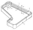
本発明の実施の形態の端末装置の構成を、図面を参照して説明する。なお、以下では、本発明に特徴的な構成(主要な構成)を中心に説明し、端末装置の全体的な構成の説明は省略する。図1は、本実施の形態の端末装置の主要な構成の説明図である。図1に示すように、本実施の形態の端末装置では、メイン基板1の上に、保護すべき情報が格納されるメモリなどの電子部品2が実装される。メイン基板1の上側には、電子部品2の上側を覆うようにサブ基板3が設けられている。また、メイン基板1の上には、電子部品2を囲うようにフレーム部材4が設けられている。フレーム部材4には、フレキシブル基板5(FPC)が巻き付けられている。フレキシブル基板5には、配線パターン6(スネークパターン)がはりめぐらされている(図2参照)。また、フレキシブル基板5は、黒色または暗色の樹脂材料(例えば、黒色のPETなど)で被覆されている。 The configuration of the terminal device according to the embodiment of the present invention will be described with reference to the drawings. In the following description, the configuration (main configuration) characteristic of the present invention will be mainly described, and description of the overall configuration of the terminal device will be omitted. FIG. 1 is an explanatory diagram of the main configuration of the terminal device according to the present embodiment. As shown in FIG. 1, in the terminal device according to the present embodiment, an electronic component 2 such as a memory storing information to be protected is mounted on a main board 1. A
ここで、図2〜図4を参照して、フレーム部材4とフレキシブル基板5の構成について、詳しく説明する。図2および図3に示すように、フレーム部材4は、メイン基板1とサブ基板3との間において電子部品2を囲う壁面部7を備えている。なお、図2および図3では、説明の便宜のため、メイン基板1とサブ基板3の図示を省略している。図4に示すように、フレキシブル基板5は、壁面部7の外側(図4における右側)を被覆するとともに、壁面部7の上側および下側(図4における上側と下側)から巻き込まれて壁面部7の内側(図4における左側)の少なくとも一部を被覆するように、フレーム部材4に巻き付けられている。 Here, the configuration of the
図1および図3に示すように、フレキシブル基板5には、メイン基板1に電気的に接続されるメイン基板片8と、サブ基板3に電気的に接続されるサブ基板片9とが延設されている。また、図2に示すように、フレーム部材4には、枠形状の3つのゴム挿着部10〜12(第1のゴム挿着部10、第2のゴム挿着部11、第3のゴム挿着部12)が設けられている。これらのゴム挿着部(第1のゴム挿着部10、第2のゴム挿着部11、第3のゴム挿着部12)は、フレーム部材4と一体に製造されてもよく、別体として製造された後にフレーム部材4に取り付けられてもよい。 As shown in FIGS. 1 and 3, the
第1のゴム挿着部10は、メイン基板片8に対応する位置に設けられ、第1のゴム挿着部10には、第1のゴム部材13が挿着される。第1のゴム部材13は、メイン基板片8に接触しており、メイン基板片8は、第1のゴム部材13の弾性力によりメイン基板1に押し付けられ、これにより、メイン基板1とメイン基板片8が電気的に接続されている。第1のゴム部材13は、サブ基板3にも接触しており、第1のゴム部材13のサブ基板3と接触する面(図2における上面)には、導電膜14が設けられている。サブ基板3には、第1のゴム部材13の導電膜14を介して電気的に接続される第1の回路パターン(図示せず)が形成されている。 The first
第2のゴム挿着部11は、サブ基板片9に対応する位置に設けられ、第2のゴム挿着部11には、第2のゴム部材15が挿着される。第2のゴム部材15は、サブ基板片9に接触しており、サブ基板片9は、第2のゴム部材15の弾性力によりサブ基板3に押し付けられ、これにより、サブ基板3とサブ基板片9が電気的に接続されている。第2のゴム部材15は、メイン基板1にも接触しており、第2のゴム部材15のメイン基板1と接触する面(図2における下面)には、導電膜16が設けられている。メイン基板1には、第2のゴム部材15の導電膜16を介して電気的に接続される第2の回路パターン(図示せず)が形成されている。 The second
第3のゴム挿着部12は、フレーム部材4の任意の隅角部に設けられ、第3のゴム挿着部12には、第3のゴム部材17が挿着される。第3のゴム部材17は、メイン基板1とサブ基板3とに接触しており、第3のゴム部材17のメイン基板1やサブ基板3と接触する面(図2における上面と下面)には、それぞれ導電膜18が設けられている。メイン基板1とサブ基板3には、第3のゴム部材17の導電膜18を介して電気的に接続される第3の回路パターン(図示せず)がそれぞれ形成されている。 The third
図5には、メイン基板1にサブ基板3を重ねた状態が示されている。この状態では、メイン基板1とメイン基板片8が電気的に接続されるとともに、サブ基板3とサブ基板片9が電気的に接続されている。すなわち、メイン基板1とサブ基板3は、フレキシブル基板5を介して電気的に接続され、フレキシブル基板5に設けられた配線パターン6と電子部品2とが電気的に接続されている。そして、フレキシブル基板5の配線パターン6の一部が切断または短絡されると、電子部品2に格納された保護すべき情報が読取り不可にされる。 FIG. 5 shows a state in which the
また、第1のゴム部材13がサブ基板3から引き離されて、第1の回路パターンの一部が切断または短絡された場合や、第2のゴム部材15がメイン基板1から引き離されて、第2の回路パターンの一部が切断または短絡された場合にも、電子部品2に格納された保護すべき情報が読取り不可にされる。さらに、第3のゴム部材17がメイン基板1またはサブ基板3から引き離されて、回路パターンの一部が切断または短絡された場合にも、電子部品2に格納された保護すべき情報が読取り不可にされる。 Further, when the
なお、電子部品2に格納された保護すべき情報を読取り不可にする方法としては、例えば、その情報を消去する方法や、または、所定の暗号化を施す方法などが利用される。 As a method for making the information to be protected stored in the electronic component 2 unreadable, for example, a method for deleting the information or a method for performing predetermined encryption is used.
このような本発明の実施の形態の端末装置によれば、電子部品2に対して不正な接触をしようとする攻撃に対して、効率よくセキュリティ性を向上することができる。 According to such a terminal device of the embodiment of the present invention, it is possible to efficiently improve security against an attack that attempts to make an unauthorized contact with the electronic component 2.
すなわち、本実施の形態では、保護すべき情報が格納される電子部品2は、メイン基板1とサブ基板3との間でフレーム部材4により囲まれ、そのフレーム部材4がフレキシブル基板5で被覆されて、フレキシブル基板5の配線パターン6と電子部品2とが電気的に接続されている。そして、電子部品2に対して不正な接触をしようとした場合、フレキシブル基板5の配線パターン6の一部が切断または短絡されると、電子部品2に格納された保護すべき情報が読取り不可にされる。この場合、フレーム部材4の壁面部7の外側だけでなく、壁面部7の上側および下側から巻き込むようにして壁面部7の内側までフレキシブル基板5によって被覆されている。したがって、基板(メイン基板1またはサブ基板3)とフレーム部材4との間に刃物を差し込んで電子部品2に不正な接触をしようとした場合でも、フレキシブル基板5の配線パターン6が切断または短絡され、電子部品2に格納された保護すべき情報が読取り不可にされる。このように、電子部品2に対して不正な接触をしようとする攻撃、特に、基板とフレーム部材4との間に刃物を差し込む攻撃に対して、セキュリティ性を向上させることができる。この場合、重要な部品(保護すべき情報が格納された電子部品2)を保護するのに必要かつ十分な部分のみをフレキシブル基板5で被覆するので、従来のように筐体の内面すべてを被覆する場合に比べて効率がよく、また、従来のように筐体の内面の一部のみを被覆する場合に比べてセキュリティ性が高い。 That is, in the present embodiment, the electronic component 2 in which information to be protected is stored is surrounded by the
また、本実施の形態では、第1のゴム部材13によりフレキシブル基板5のメイン基板片8がメイン基板1に押し付けられるとともに、第2のゴム部材15によりフレキシブル基板5のサブ基板片9がサブ基板3に押し付けられる。このように、ゴム部材(第1のゴム部材13と第2のゴム部材15)の弾性力を利用して、メイン基板1とサブ基板3がフレキシブル基板5を介して電気的に接続される。そして電子部品2に不正な接触をしようとした場合、フレキシブル基板5の配線パターン6の一部が切断または短絡されると、電子部品2に格納された保護すべき情報が読取り不可にされる。 In the present embodiment, the main board piece 8 of the
また、本実施の形態では、第1のゴム部材13の導電膜14を介して、サブ基板3に設けられた第1の回路パターンが電気的に接続される。そして、電子部品2に不正な接触をしようとした場合に、第1のゴム部材13がサブ基板3から引き離されると、第1の回路パターンの一部が切断または短絡され、電子部品2に格納された保護すべき情報が読取り不可にされる。 In the present embodiment, the first circuit pattern provided on the
また、本実施の形態では、第2のゴム部材15の導電膜16を介して、メイン基板1に設けられた第2の回路パターンが電気的に接続される。そして、電子部品2に不正な接触をしようとした場合に、第2のゴム部材15がメイン基板1から引き離されると、第2の回路パターンの一部が切断または短絡され、電子部品2に格納された保護すべき情報が読取り不可にされる。 In the present embodiment, the second circuit pattern provided on the main substrate 1 is electrically connected through the
また、本実施の形態では、メイン基板1とサブ基板3との間には、メイン基板1とサブ基板3と接触する二つの面にそれぞれ導電膜18が設けられた第3のゴム部材17が設けられ、第3のゴム部材17の導電膜18を介して、メイン基板1またはサブ基板3に設けられた第3の回路パターンがそれぞれ電気的に接続される。そして、電子部品2に不正な接触をしようとした場合に、第3のゴム部材17がメイン基板1またはサブ基板3から引き離されると、メイン基板1またはサブ基板3の第3の回路パターンの一部が切断または短絡され、電子部品2に格納された保護すべき情報が読取り不可にされる。 In the present embodiment, a
また、本実施の形態では、フレキシブル基板5が黒色の樹脂材料で被覆されるので、フレキシブル基板5に設けられた配線パターン6を外部から視認することが困難になる。したがって、配線パターン6の間に刃物を差し込む攻撃に対して、セキュリティ性が向上させることができる。 Moreover, in this Embodiment, since the
以上、本発明の実施の形態を例示により説明したが、本発明の範囲はこれらに限定されるものではなく、請求項に記載された範囲内において目的に応じて変更・変形することが可能である。 The embodiments of the present invention have been described above by way of example, but the scope of the present invention is not limited to these embodiments, and can be changed or modified according to the purpose within the scope of the claims. is there.
以上のように、本発明にかかる端末装置は、電子部品に対して不正な接触をしようとする攻撃に対して、効率よくセキュリティ性を向上することができるという効果を有し、クレジットカードやICカードを用いて決済を行う決済端末装置等として有用である。 As described above, the terminal device according to the present invention has an effect that it is possible to efficiently improve security against an attack that attempts to make unauthorized contact with an electronic component. It is useful as a payment terminal device that performs payment using a card.
1 メイン基板(第1の基板)
2 電子部品
3 サブ基板(第2の基板)
4 フレーム部材
5 フレキシブル基板
6 配線パターン
7 壁面部
8 メイン基板片(第1の基板片)
9 サブ基板片(第2の基板片)
10 第1のゴム挿着部
11 第2のゴム挿着部
12 第3のゴム挿着部
13 第1のゴム部材
14 導電膜(第1の導電膜)
15 第2のゴム部材
16 導電膜(第2の導電膜)
17 第3のゴム部材
18 導電膜(第3の導電膜)1 Main board (first board)
2
4
9 Sub board piece (second board piece)
DESCRIPTION OF
15
17
Claims (6)
Translated fromJapanese前記第1の基板に実装され、保護すべき情報が格納される電子部品と、
前記第1の基板の上側に設けられ、前記電子部品の上側を覆う第2の基板と、
前記第1の基板と前記第2の基板との間に設けられ、前記電子部品を囲う壁面部を有するフレーム部材と、
前記壁面部の外側を被覆するとともに、前記壁面部の上側および下側から巻き込まれて前記壁面部の内側の少なくとも一部を被覆するフレキシブル基板と、
を備え、
前記フレキシブル基板に設けられた配線パターンと前記電子部品とが電気的に接続されており、前記配線パターンの一部が切断または短絡されると、前記電子部品に格納された前記保護すべき情報が読取り不可にされることを特徴とする端末装置。A first substrate;
An electronic component mounted on the first board and storing information to be protected;
A second substrate provided on an upper side of the first substrate and covering an upper side of the electronic component;
A frame member provided between the first substrate and the second substrate and having a wall surface portion surrounding the electronic component;
A flexible substrate that covers the outside of the wall surface portion and is wound from above and below the wall surface portion to cover at least a part of the inside of the wall surface portion;
With
When the wiring pattern provided on the flexible substrate and the electronic component are electrically connected and a part of the wiring pattern is cut or short-circuited, the information to be protected stored in the electronic component is A terminal device that is made unreadable.
前記フレーム部材は、前記第1の基板片に対応する位置に第1のゴム部材を挿着するための第1のゴム挿着部と、前記第2の基板片に対応する位置に第2のゴム部材を挿着するための第2のゴム挿着部とを備え、
前記第1の基板片は、前記第1のゴム部材の弾性力により前記第1の基板に押し付けられ、前記第2の基板片は、前記第2のゴム部材の弾性力により前記第2の基板に押し付けられ、
前記第1の基板と前記第2の基板は、前記フレキシブル基板を介して電気的に接続され、前記配線パターンの一部が切断または短絡されると、前記電子部品に格納された前記保護すべき情報が読取り不可にされることを特徴とする請求項1に記載の端末装置。The flexible substrate includes a first substrate piece electrically connected to the first substrate, and a second substrate piece electrically connected to the second substrate,
The frame member includes a first rubber insertion portion for inserting the first rubber member at a position corresponding to the first substrate piece, and a second position at a position corresponding to the second substrate piece. A second rubber insertion portion for inserting the rubber member,
The first substrate piece is pressed against the first substrate by the elastic force of the first rubber member, and the second substrate piece is pressed by the elastic force of the second rubber member. Pressed against
The first substrate and the second substrate are electrically connected via the flexible substrate, and when a part of the wiring pattern is cut or short-circuited, the protection stored in the electronic component should be protected. 2. The terminal device according to claim 1, wherein information is made unreadable.
前記第1のゴム部材が前記第2の基板から引き離されて、前記第1の回路パターンの一部が切断または短絡されると、前記電子部品に格納された前記保護すべき情報が読取り不可にされることを特徴とする請求項2に記載の端末装置。The first rubber member is provided with a first conductive film at least on a surface in contact with the second substrate, and is electrically connected to the second substrate via the first conductive film. A first circuit pattern is formed,
When the first rubber member is pulled away from the second substrate and a part of the first circuit pattern is cut or short-circuited, the information to be protected stored in the electronic component becomes unreadable. The terminal device according to claim 2, wherein:
前記第2のゴム部材が前記第1の基板から引き離されて、前記第2の回路パターンの一部が切断または短絡されると、前記電子部品に格納された前記保護すべき情報が読取り不可にされることを特徴とする請求項2または請求項3に記載の端末装置。The second rubber member is provided with a second conductive film at least on a surface in contact with the first substrate, and is electrically connected to the first substrate through the second conductive film. A second circuit pattern is formed,
When the second rubber member is separated from the first substrate and a part of the second circuit pattern is cut or short-circuited, the information to be protected stored in the electronic component becomes unreadable. The terminal device according to claim 2 or claim 3, wherein
前記第3のゴム部材が前記第1の基板または前記第2の基板から引き離されて、前記第3の回路パターンの一部が切断または短絡されると、前記電子部品に格納された前記保護すべき情報が読取り不可にされることを特徴とする請求項1ないし請求項4のいずれかに記載の端末装置。A third rubber member provided with a third conductive film on each of two surfaces in contact with the first substrate and the second substrate between the first substrate and the second substrate. And a third circuit pattern electrically formed through the third conductive film is formed on each of the first substrate and the second substrate,
Whenthe third rubber member is pulled away from the first substrate or the second substrate and a part of the third circuit pattern is cut or short-circuited, the protection stored in the electronic component is protected. The terminal device according to any one of claims 1 to 4, wherein power information is made unreadable.
Priority Applications (7)
| Application Number | Priority Date | Filing Date | Title |
|---|---|---|---|
| JP2011194187AJP4914530B1 (en) | 2011-09-06 | 2011-09-06 | Terminal device |
| US13/596,762US9036366B2 (en) | 2011-09-06 | 2012-08-28 | Terminal unit |
| EP12766166.8AEP2754337A1 (en) | 2011-09-06 | 2012-08-31 | Terminal unit with security features |
| CN201610905911.8ACN106879160B (en) | 2011-09-06 | 2012-08-31 | Terminal device with security feature |
| CN201280040976.0ACN103748973B (en) | 2011-09-06 | 2012-08-31 | End Units with Safety Features |
| PCT/JP2012/005511WO2013035284A1 (en) | 2011-09-06 | 2012-08-31 | Terminal unit with security features |
| US14/684,857US9215799B2 (en) | 2011-09-06 | 2015-04-13 | Terminal unit |
Applications Claiming Priority (1)
| Application Number | Priority Date | Filing Date | Title |
|---|---|---|---|
| JP2011194187AJP4914530B1 (en) | 2011-09-06 | 2011-09-06 | Terminal device |
Publications (2)
| Publication Number | Publication Date |
|---|---|
| JP4914530B1true JP4914530B1 (en) | 2012-04-11 |
| JP2013054689A JP2013054689A (en) | 2013-03-21 |
Family
ID=46170981
Family Applications (1)
| Application Number | Title | Priority Date | Filing Date |
|---|---|---|---|
| JP2011194187AActiveJP4914530B1 (en) | 2011-09-06 | 2011-09-06 | Terminal device |
Country Status (5)
| Country | Link |
|---|---|
| US (2) | US9036366B2 (en) |
| EP (1) | EP2754337A1 (en) |
| JP (1) | JP4914530B1 (en) |
| CN (2) | CN103748973B (en) |
| WO (1) | WO2013035284A1 (en) |
Cited By (3)
| Publication number | Priority date | Publication date | Assignee | Title |
|---|---|---|---|---|
| CN103578201A (en)* | 2012-07-27 | 2014-02-12 | 德昌电机(深圳)有限公司 | Security wrap and method for forming and installing same |
| JP2014028115A (en)* | 2012-06-27 | 2014-02-13 | Sammy Corp | Board case unit |
| CN107105573A (en)* | 2017-05-24 | 2017-08-29 | 广东欧珀移动通信有限公司 | Electronic component support, electronic component module and mobile terminal |
Families Citing this family (9)
| Publication number | Priority date | Publication date | Assignee | Title |
|---|---|---|---|---|
| US9049784B2 (en) | 2011-11-24 | 2015-06-02 | Joled Inc. | Flexible display including a flexible display panel having an opening |
| CN203722975U (en)* | 2013-11-19 | 2014-07-16 | 中兴通讯股份有限公司 | Heat-dissipation device for mobile terminal, and shielding case frame |
| US9521764B2 (en)* | 2013-12-09 | 2016-12-13 | Timothy Steiner | Tamper respondent apparatus |
| JP6384774B2 (en) | 2014-03-11 | 2018-09-05 | パナソニックIpマネジメント株式会社 | Terminal |
| JP5703453B1 (en)* | 2014-03-28 | 2015-04-22 | パナソニックIpマネジメント株式会社 | Information processing device |
| JP5656303B1 (en) | 2014-03-28 | 2015-01-21 | パナソニック株式会社 | Information processing device |
| JP2018010365A (en)* | 2016-07-11 | 2018-01-18 | 沖電気工業株式会社 | Pin pad |
| JP6598312B2 (en)* | 2017-12-08 | 2019-10-30 | Necプラットフォームズ株式会社 | Enclosure device and electronic device |
| FR3115897B1 (en)* | 2020-11-04 | 2023-06-09 | Banks And Acquirers Int Holding | Security module, electronic payment terminal, corresponding detection method. |
Citations (6)
| Publication number | Priority date | Publication date | Assignee | Title |
|---|---|---|---|---|
| JPH03105538A (en)* | 1989-09-12 | 1991-05-02 | Internatl Business Mach Corp <Ibm> | Defence barrier for infiltration into electronic assembly |
| JPH10214234A (en)* | 1997-01-29 | 1998-08-11 | Hitachi Software Eng Co Ltd | Ic card |
| JPH11353237A (en)* | 1998-06-05 | 1999-12-24 | Fujitsu Ltd | Electronic trading device |
| JP2001242951A (en)* | 2000-02-28 | 2001-09-07 | Matsushita Electric Ind Co Ltd | Terminal device |
| JP2008033593A (en)* | 2006-07-28 | 2008-02-14 | Sony Corp | Data storage device, data protection method and communication equipment |
| JP2011129011A (en)* | 2009-12-21 | 2011-06-30 | Denso Wave Inc | Personal digital assistant |
Family Cites Families (23)
| Publication number | Priority date | Publication date | Assignee | Title |
|---|---|---|---|---|
| US3877064A (en)* | 1974-02-22 | 1975-04-08 | Amp Inc | Device for connecting leadless integrated circuit packages to a printed-circuit board |
| US4359222A (en)* | 1978-10-30 | 1982-11-16 | Smith Engineering | Hand-held electronic game playing device with replaceable cartridges |
| US4354720A (en)* | 1980-10-20 | 1982-10-19 | Amp Incorporated | Connector assembly having improved latching means |
| US4449770A (en)* | 1981-05-22 | 1984-05-22 | Amp Incorporated | Socketless separable connector |
| US4395084A (en)* | 1981-07-06 | 1983-07-26 | Teledyne Industries, Inc. | Electrical socket for leadless integrated circuit packages |
| US4504887A (en)* | 1983-04-01 | 1985-03-12 | Amp Incorporated | Leadless integrated circuit package housing having means for contact replacement |
| JPS61219926A (en) | 1985-03-26 | 1986-09-30 | Seiwa Seisakusho:Kk | Manufacture of spectacles |
| US4810917A (en)* | 1985-05-28 | 1989-03-07 | Autotech Corporation | Digital resolver/encoder assembly |
| US4655519A (en)* | 1985-10-16 | 1987-04-07 | Amp Incorporated | Electrical connector for interconnecting arrays of conductive areas |
| US4647124A (en)* | 1985-10-16 | 1987-03-03 | Amp Incorporated | Electrical connector for interconnecting arrays of conductive areas |
| US4873615A (en)* | 1986-10-09 | 1989-10-10 | Amp Incorporated | Semiconductor chip carrier system |
| US5199889A (en)* | 1991-11-12 | 1993-04-06 | Jem Tech | Leadless grid array socket |
| JP2002176239A (en) | 2000-12-06 | 2002-06-21 | Agilent Technologies Japan Ltd | Connector and connecting method of high frequency circuit board |
| US6853093B2 (en) | 2002-12-20 | 2005-02-08 | Lipman Electronic Engineering Ltd. | Anti-tampering enclosure for electronic circuitry |
| US7625216B2 (en)* | 2003-06-11 | 2009-12-01 | Cinch Connectors, Inc. | Electrical connector |
| KR100578919B1 (en)* | 2003-11-26 | 2006-05-11 | 삼성에스디아이 주식회사 | Plasma Display Apparatus And TC Applied To The Apparatus And Manufacturing Method Thereof |
| US6996953B2 (en) | 2004-01-23 | 2006-02-14 | Pitney Bowes Inc. | System and method for installing a tamper barrier wrap in a PCB assembly, including a PCB assembly having improved heat sinking |
| KR100730138B1 (en)* | 2005-06-28 | 2007-06-19 | 삼성에스디아이 주식회사 | Plasma display device |
| CN101253823A (en)* | 2005-06-30 | 2008-08-27 | 西门子公司 | Hardware protection against external manipulation of sensitive electronic data components |
| WO2007003228A1 (en)* | 2005-06-30 | 2007-01-11 | Siemens Aktiengesellschaft | Hardware protection system for sensitive electronic-data modules protecting against external manipulations |
| CN100464340C (en)* | 2007-09-21 | 2009-02-25 | 百富计算机技术(深圳)有限公司 | safety box |
| US8238095B2 (en)* | 2009-08-31 | 2012-08-07 | Ncr Corporation | Secure circuit board assembly |
| CN102238806A (en)* | 2010-04-28 | 2011-11-09 | 富葵精密组件(深圳)有限公司 | Circuit board module |
- 2011
- 2011-09-06JPJP2011194187Apatent/JP4914530B1/enactiveActive
- 2012
- 2012-08-28USUS13/596,762patent/US9036366B2/ennot_activeExpired - Fee Related
- 2012-08-31EPEP12766166.8Apatent/EP2754337A1/ennot_activeWithdrawn
- 2012-08-31CNCN201280040976.0Apatent/CN103748973B/ennot_activeExpired - Fee Related
- 2012-08-31WOPCT/JP2012/005511patent/WO2013035284A1/enactiveApplication Filing
- 2012-08-31CNCN201610905911.8Apatent/CN106879160B/ennot_activeExpired - Fee Related
- 2015
- 2015-04-13USUS14/684,857patent/US9215799B2/ennot_activeExpired - Fee Related
Patent Citations (6)
| Publication number | Priority date | Publication date | Assignee | Title |
|---|---|---|---|---|
| JPH03105538A (en)* | 1989-09-12 | 1991-05-02 | Internatl Business Mach Corp <Ibm> | Defence barrier for infiltration into electronic assembly |
| JPH10214234A (en)* | 1997-01-29 | 1998-08-11 | Hitachi Software Eng Co Ltd | Ic card |
| JPH11353237A (en)* | 1998-06-05 | 1999-12-24 | Fujitsu Ltd | Electronic trading device |
| JP2001242951A (en)* | 2000-02-28 | 2001-09-07 | Matsushita Electric Ind Co Ltd | Terminal device |
| JP2008033593A (en)* | 2006-07-28 | 2008-02-14 | Sony Corp | Data storage device, data protection method and communication equipment |
| JP2011129011A (en)* | 2009-12-21 | 2011-06-30 | Denso Wave Inc | Personal digital assistant |
Cited By (3)
| Publication number | Priority date | Publication date | Assignee | Title |
|---|---|---|---|---|
| JP2014028115A (en)* | 2012-06-27 | 2014-02-13 | Sammy Corp | Board case unit |
| CN103578201A (en)* | 2012-07-27 | 2014-02-12 | 德昌电机(深圳)有限公司 | Security wrap and method for forming and installing same |
| CN107105573A (en)* | 2017-05-24 | 2017-08-29 | 广东欧珀移动通信有限公司 | Electronic component support, electronic component module and mobile terminal |
Also Published As
| Publication number | Publication date |
|---|---|
| EP2754337A1 (en) | 2014-07-16 |
| WO2013035284A1 (en) | 2013-03-14 |
| JP2013054689A (en) | 2013-03-21 |
| CN103748973A (en) | 2014-04-23 |
| CN103748973B (en) | 2016-11-23 |
| CN106879160A (en) | 2017-06-20 |
| US9036366B2 (en) | 2015-05-19 |
| US9215799B2 (en) | 2015-12-15 |
| US20150223327A1 (en) | 2015-08-06 |
| CN106879160B (en) | 2018-06-26 |
| US20130058057A1 (en) | 2013-03-07 |
Similar Documents
| Publication | Publication Date | Title |
|---|---|---|
| JP4914530B1 (en) | Terminal device | |
| US8589703B2 (en) | Tamper respondent covering | |
| US7549064B2 (en) | Secure circuit assembly | |
| US10595400B1 (en) | Tamper detection system | |
| US20100024046A1 (en) | Methods and systems for detecting a lateral intrusion of a secure electronic component enclosure | |
| US8251289B2 (en) | Data protecting electronic device | |
| CN101454784B (en) | Device to shield against interference from electrical appliances | |
| US11416690B2 (en) | Memory card reader body with protective mesh on both sides | |
| JP5455250B2 (en) | Information processing device | |
| US8573989B2 (en) | Memory card reader | |
| KR101402827B1 (en) | Pin pad and security method thereof | |
| BR102012010461B1 (en) | SYSTEM FOR MECHANICAL AND ELECTRONIC PROTECTION OF SAFE EQUIPMENT | |
| JP5829642B2 (en) | Electronics | |
| JP5703453B1 (en) | Information processing device | |
| JP2008130737A (en) | Circuit board with electronic circuit component | |
| CA2984478C (en) | Detection of the opening of a data input device | |
| US7645951B2 (en) | Device for protecting data stored in a switching arrangement that consists of electronic components and a processor | |
| CN205608734U (en) | Finance equipment and protection device thereof | |
| CN206460467U (en) | The equipment of resistance against physical attack | |
| EP3644209B1 (en) | Tamper sensor | |
| JP6268500B2 (en) | Transaction terminal device and security module | |
| JP2016146036A (en) | Card connector |
Legal Events
| Date | Code | Title | Description |
|---|---|---|---|
| TRDD | Decision of grant or rejection written | ||
| A01 | Written decision to grant a patent or to grant a registration (utility model) | Free format text:JAPANESE INTERMEDIATE CODE: A01 | |
| A61 | First payment of annual fees (during grant procedure) | Free format text:JAPANESE INTERMEDIATE CODE: A61 Effective date:20120120 | |
| R150 | Certificate of patent or registration of utility model | Ref document number:4914530 Country of ref document:JP Free format text:JAPANESE INTERMEDIATE CODE: R150 Free format text:JAPANESE INTERMEDIATE CODE: R150 | |
| FPAY | Renewal fee payment (event date is renewal date of database) | Free format text:PAYMENT UNTIL: 20150127 Year of fee payment:3 |