JP4912917B2 - Circuit board, portable electronic device, and circuit board manufacturing method - Google Patents
Circuit board, portable electronic device, and circuit board manufacturing methodDownload PDFInfo
- Publication number
- JP4912917B2 JP4912917B2JP2007041755AJP2007041755AJP4912917B2JP 4912917 B2JP4912917 B2JP 4912917B2JP 2007041755 AJP2007041755 AJP 2007041755AJP 2007041755 AJP2007041755 AJP 2007041755AJP 4912917 B2JP4912917 B2JP 4912917B2
- Authority
- JP
- Japan
- Prior art keywords
- circuit board
- land
- pad
- conductive
- pads
- Prior art date
- Legal status (The legal status is an assumption and is not a legal conclusion. Google has not performed a legal analysis and makes no representation as to the accuracy of the status listed.)
- Expired - Fee Related
Links
Images


Classifications
- H—ELECTRICITY
- H05—ELECTRIC TECHNIQUES NOT OTHERWISE PROVIDED FOR
- H05K—PRINTED CIRCUITS; CASINGS OR CONSTRUCTIONAL DETAILS OF ELECTRIC APPARATUS; MANUFACTURE OF ASSEMBLAGES OF ELECTRICAL COMPONENTS
- H05K1/00—Printed circuits
- H05K1/02—Details
- H05K1/0266—Marks, test patterns or identification means
- H05K1/0268—Marks, test patterns or identification means for electrical inspection or testing
- H—ELECTRICITY
- H05—ELECTRIC TECHNIQUES NOT OTHERWISE PROVIDED FOR
- H05K—PRINTED CIRCUITS; CASINGS OR CONSTRUCTIONAL DETAILS OF ELECTRIC APPARATUS; MANUFACTURE OF ASSEMBLAGES OF ELECTRICAL COMPONENTS
- H05K1/00—Printed circuits
- H05K1/02—Details
- H05K1/0286—Programmable, customizable or modifiable circuits
- H05K1/0293—Individual printed conductors which are adapted for modification, e.g. fusable or breakable conductors, printed switches
- H—ELECTRICITY
- H05—ELECTRIC TECHNIQUES NOT OTHERWISE PROVIDED FOR
- H05K—PRINTED CIRCUITS; CASINGS OR CONSTRUCTIONAL DETAILS OF ELECTRIC APPARATUS; MANUFACTURE OF ASSEMBLAGES OF ELECTRICAL COMPONENTS
- H05K3/00—Apparatus or processes for manufacturing printed circuits
- H05K3/30—Assembling printed circuits with electric components, e.g. with resistor
- H05K3/32—Assembling printed circuits with electric components, e.g. with resistor electrically connecting electric components or wires to printed circuits
- H05K3/34—Assembling printed circuits with electric components, e.g. with resistor electrically connecting electric components or wires to printed circuits by soldering
- H05K3/3457—Solder materials or compositions; Methods of application thereof
- H05K3/3485—Applying solder paste, slurry or powder
- H—ELECTRICITY
- H05—ELECTRIC TECHNIQUES NOT OTHERWISE PROVIDED FOR
- H05K—PRINTED CIRCUITS; CASINGS OR CONSTRUCTIONAL DETAILS OF ELECTRIC APPARATUS; MANUFACTURE OF ASSEMBLAGES OF ELECTRICAL COMPONENTS
- H05K2201/00—Indexing scheme relating to printed circuits covered by H05K1/00
- H05K2201/09—Shape and layout
- H05K2201/09818—Shape or layout details not covered by a single group of H05K2201/09009 - H05K2201/09809
- H05K2201/0989—Coating free areas, e.g. areas other than pads or lands free of solder resist
- H—ELECTRICITY
- H05—ELECTRIC TECHNIQUES NOT OTHERWISE PROVIDED FOR
- H05K—PRINTED CIRCUITS; CASINGS OR CONSTRUCTIONAL DETAILS OF ELECTRIC APPARATUS; MANUFACTURE OF ASSEMBLAGES OF ELECTRICAL COMPONENTS
- H05K2201/00—Indexing scheme relating to printed circuits covered by H05K1/00
- H05K2201/10—Details of components or other objects attached to or integrated in a printed circuit board
- H05K2201/10613—Details of electrical connections of non-printed components, e.g. special leads
- H05K2201/10621—Components characterised by their electrical contacts
- H05K2201/10636—Leadless chip, e.g. chip capacitor or resistor
- H—ELECTRICITY
- H05—ELECTRIC TECHNIQUES NOT OTHERWISE PROVIDED FOR
- H05K—PRINTED CIRCUITS; CASINGS OR CONSTRUCTIONAL DETAILS OF ELECTRIC APPARATUS; MANUFACTURE OF ASSEMBLAGES OF ELECTRICAL COMPONENTS
- H05K2203/00—Indexing scheme relating to apparatus or processes for manufacturing printed circuits covered by H05K3/00
- H05K2203/05—Patterning and lithography; Masks; Details of resist
- H05K2203/0502—Patterning and lithography
- H05K2203/0545—Pattern for applying drops or paste; Applying a pattern made of drops or paste
- H—ELECTRICITY
- H05—ELECTRIC TECHNIQUES NOT OTHERWISE PROVIDED FOR
- H05K—PRINTED CIRCUITS; CASINGS OR CONSTRUCTIONAL DETAILS OF ELECTRIC APPARATUS; MANUFACTURE OF ASSEMBLAGES OF ELECTRICAL COMPONENTS
- H05K2203/00—Indexing scheme relating to apparatus or processes for manufacturing printed circuits covered by H05K3/00
- H05K2203/16—Inspection; Monitoring; Aligning
- H05K2203/162—Testing a finished product, e.g. heat cycle testing of solder joints
- H—ELECTRICITY
- H05—ELECTRIC TECHNIQUES NOT OTHERWISE PROVIDED FOR
- H05K—PRINTED CIRCUITS; CASINGS OR CONSTRUCTIONAL DETAILS OF ELECTRIC APPARATUS; MANUFACTURE OF ASSEMBLAGES OF ELECTRICAL COMPONENTS
- H05K2203/00—Indexing scheme relating to apparatus or processes for manufacturing printed circuits covered by H05K3/00
- H05K2203/16—Inspection; Monitoring; Aligning
- H05K2203/168—Wrong mounting prevention
- H—ELECTRICITY
- H05—ELECTRIC TECHNIQUES NOT OTHERWISE PROVIDED FOR
- H05K—PRINTED CIRCUITS; CASINGS OR CONSTRUCTIONAL DETAILS OF ELECTRIC APPARATUS; MANUFACTURE OF ASSEMBLAGES OF ELECTRICAL COMPONENTS
- H05K2203/00—Indexing scheme relating to apparatus or processes for manufacturing printed circuits covered by H05K3/00
- H05K2203/17—Post-manufacturing processes
- H05K2203/175—Configurations of connections suitable for easy deletion, e.g. modifiable circuits or temporary conductors for electroplating; Processes for deleting connections
- H—ELECTRICITY
- H05—ELECTRIC TECHNIQUES NOT OTHERWISE PROVIDED FOR
- H05K—PRINTED CIRCUITS; CASINGS OR CONSTRUCTIONAL DETAILS OF ELECTRIC APPARATUS; MANUFACTURE OF ASSEMBLAGES OF ELECTRICAL COMPONENTS
- H05K3/00—Apparatus or processes for manufacturing printed circuits
- H05K3/30—Assembling printed circuits with electric components, e.g. with resistor
- H05K3/32—Assembling printed circuits with electric components, e.g. with resistor electrically connecting electric components or wires to printed circuits
- H05K3/34—Assembling printed circuits with electric components, e.g. with resistor electrically connecting electric components or wires to printed circuits by soldering
- H05K3/3452—Solder masks
- Y—GENERAL TAGGING OF NEW TECHNOLOGICAL DEVELOPMENTS; GENERAL TAGGING OF CROSS-SECTIONAL TECHNOLOGIES SPANNING OVER SEVERAL SECTIONS OF THE IPC; TECHNICAL SUBJECTS COVERED BY FORMER USPC CROSS-REFERENCE ART COLLECTIONS [XRACs] AND DIGESTS
- Y02—TECHNOLOGIES OR APPLICATIONS FOR MITIGATION OR ADAPTATION AGAINST CLIMATE CHANGE
- Y02P—CLIMATE CHANGE MITIGATION TECHNOLOGIES IN THE PRODUCTION OR PROCESSING OF GOODS
- Y02P70/00—Climate change mitigation technologies in the production process for final industrial or consumer products
- Y02P70/50—Manufacturing or production processes characterised by the final manufactured product
- Y—GENERAL TAGGING OF NEW TECHNOLOGICAL DEVELOPMENTS; GENERAL TAGGING OF CROSS-SECTIONAL TECHNOLOGIES SPANNING OVER SEVERAL SECTIONS OF THE IPC; TECHNICAL SUBJECTS COVERED BY FORMER USPC CROSS-REFERENCE ART COLLECTIONS [XRACs] AND DIGESTS
- Y10—TECHNICAL SUBJECTS COVERED BY FORMER USPC
- Y10T—TECHNICAL SUBJECTS COVERED BY FORMER US CLASSIFICATION
- Y10T29/00—Metal working
- Y10T29/49—Method of mechanical manufacture
- Y10T29/49002—Electrical device making
- Y10T29/49117—Conductor or circuit manufacturing
- Y10T29/49124—On flat or curved insulated base, e.g., printed circuit, etc.
- Y10T29/4913—Assembling to base an electrical component, e.g., capacitor, etc.
Landscapes
- Engineering & Computer Science (AREA)
- Microelectronics & Electronic Packaging (AREA)
- Manufacturing & Machinery (AREA)
- Electric Connection Of Electric Components To Printed Circuits (AREA)
- Printing Elements For Providing Electric Connections Between Printed Circuits (AREA)
- Battery Mounting, Suspending (AREA)
Description
Translated fromJapanese本発明は、所定の回路パターンが形成された回路基板、携帯電子機器および回路基板の製造方法に関する。 The present invention relates to a circuit board on which a predetermined circuit pattern is formed, a portable electronic device, and a circuit board manufacturing method.
一般的に回路基板の設計においては、基板に形成する回路の設計、設計値に従った回路基板の製造、及び製造された回路基板の試験が順に行われる。試験により不具合が見つかった場合には、意図通りの回路が形成されるまで、回路の設計変更、設計変更した回路基板の製造、及びその回路基板の試験が繰り返し行われる。
従来は、回路基板の試験を容易にするために、設計の段階で予め0Ωの抵抗素子(検査ポイント)を盛り込んだ回路を設計しておき、開発・設計・生産時には0Ω抵抗素子によって回路の所定の部分を敢えてショート(短絡)させたり、試験・修理時には0Ω抵抗素子を外し、0Ω抵抗素子に流れる電量の検出等を行ったりすることにより回路基板の試験が行われる。ここで、0Ω素子とは、チップ抵抗素子或いはリード線型抵抗素子と同様の形状をした、抵抗値が極めて小さい抵抗素子である。In general, in designing a circuit board, a circuit to be formed on the board, a circuit board according to the design value, and a test of the manufactured circuit board are sequentially performed. When a defect is found by the test, the design change of the circuit, the manufacture of the circuit board with the changed design, and the test of the circuit board are repeatedly performed until the intended circuit is formed.
Conventionally, in order to facilitate the testing of circuit boards, a circuit including a 0Ω resistance element (inspection point) is designed in advance at the design stage, and the circuit is specified by the 0Ω resistance element during development, design, and production. The circuit board is tested by deliberately short-circuiting this part, or by removing the 0Ω resistance element during testing / repair and detecting the amount of electricity flowing through the 0Ω resistance element. Here, the 0Ω element is a resistance element having a very small resistance value and having the same shape as the chip resistance element or the lead wire resistance element.
0Ω抵抗素子は回路構成上本来必要なものではないので、回路基板の設計が終了して回路基板を量産する際にはすべてパターン(配線)化し削除することが望ましい。しかし、0Ω抵抗を利用すれば、回路基板の量産時に生じてしまう不良基板を簡便に検査することができるので、0Ω素子が搭載された状態で回路基板が量産されてしまう場合が多い。
例えば、特許文献1及び特許文献2には、回路基板上に検査ポイントを搭載する技術が開示されている。Since the 0Ω resistance element is not essentially required in terms of the circuit configuration, it is desirable that all the patterns (wiring) be removed when the circuit board is designed and mass-produced. However, if a 0Ω resistor is used, a defective substrate that occurs during mass production of a circuit board can be easily inspected, so that circuit boards are often mass-produced with a 0Ω element mounted.
For example,
0Ω抵抗素子を予め基板上に形成しない場合は、不良基板の検査時等に、基板上の各電子部品に対して動作確認を行う際には、1つ1つ実装されている電子部品を取り外して検査を行う必要がある。しかし、実装された電子部品は取り外される際に壊れてしまう危険性がある、という不利益があった。こうした不利益を解消する技術として特許文献3に開示された技術がある。
特許文献1に開示された技術は、プリント配線板における所定の回路パターン中において、対の関係をもって相互に近接配置された複数組のジャンパランド等を0Ωチップ抵抗部品を介して相互に選択的に接続するように構成したジャンパランドの接続構造が開示されている。
しかし、上述した特許文献1に開示された技術には、0Ωチップ抵抗部品を搭載する分だけ部品コストを要するとともに、通常の工程の他に0Ωの部品を実装するための工程が必要となる、という不利益がある。In the technique disclosed in
However, the technique disclosed in
特許文献2には、基板上の厚膜金属からなる回路の一部に設けた遮断部分で回路検査をしてから、前記遮断部分を導通させて閉回路を構成する厚膜混成集積回路パターンにおいて、前記厚膜金属による略円形の搭載部品取り付けランドを形成し、前記部品取り付けランドを部品取り付け方向に対し斜め方向に切断分割した前記遮断部分を設けた厚膜混成集積回路パターンが開示されている。
しかし、特許文献2に開示された技術には、部品点数が増大してしまう、という不利益があった。Patent Document 2 discloses a thick film hybrid integrated circuit pattern in which a closed circuit is formed by conducting a circuit inspection at a blocking portion provided in a part of a circuit made of a thick film metal on a substrate and then conducting the blocking portion. A thick film hybrid integrated circuit pattern is disclosed in which a substantially circular mounting component mounting land is formed of the thick film metal, and the blocking portion is formed by cutting and dividing the component mounting land in an oblique direction with respect to the component mounting direction. .
However, the technique disclosed in Patent Document 2 has a disadvantage that the number of parts increases.
特許文献3には、絶縁材料からなる基体と、基体の下面中央に第1の凹部を設け、第1の凹部を横切るように第2の凹部を複数並列に第1の凹部より深く設け、基体の下面
に複数の相対する脚部を設け、複数の相対する脚部を結ぶように脚部の下面を含む外周面から該第1の凹部の内面に導電層を設け、複数の導電路を設けるジャンパチップが開示されている。
しかし、量産される回路基板に0Ω抵抗素子を搭載すると検査が容易になるという利点があるが、0Ω抵抗素子を搭載する分だけ部品コストを要するとともにその実装コストが必要になるため、回路基板のコストが上昇する、というコスト面の不利益があった。また、0Ω抵抗素子には通常の抵抗素子と同様の確率で搭載不良が生じるため。搭載数量に比例して回路基板の製造歩留まりが低下する、という不利益があった。In Patent Document 3, a base made of an insulating material, a first recess is provided at the center of the lower surface of the base, and a plurality of second recesses are provided in parallel to the first recess so as to cross the first recess. A plurality of opposite leg portions are provided on the lower surface of the base plate, a conductive layer is provided on the inner surface of the first recess from the outer peripheral surface including the lower surface of the leg portion so as to connect the plurality of opposite leg portions, and a plurality of conductive paths are provided. A jumper chip is disclosed.
However, mounting a 0Ω resistance element on a mass-produced circuit board has the advantage that the inspection becomes easy. However, as the 0Ω resistance element is mounted, the component cost and the mounting cost are required. There was a cost penalty that the cost would rise. In addition, mounting failure occurs in the 0Ω resistance element with the same probability as a normal resistance element. There was a disadvantage that the production yield of the circuit board was lowered in proportion to the number of mounted devices.
本発明は、上述した不利益を解消するために、コスト低減及び歩留まり向上を図りつつ容易に検査を行うことができる回路基板、携帯電子機器及び回路基板の製造方法を提供することを目的とする。 In order to eliminate the above-described disadvantages, an object of the present invention is to provide a circuit board, a portable electronic device, and a method for manufacturing the circuit board that can be easily inspected while reducing costs and improving yield. .
上述した目的を達成するために、第1の発明の回路基板は、配線パターンと、前記配線パターンに接続される複数のランドパッドと、前記ランドパッドを露出させる開口部を有し、基板表面に形成されたレジストと、前記複数のランドパッドのうち少なくとも1つに実装される電子部品と、を備える回路基板において、前記複数のランドパッドは、前記電子部品が実装されず、かつ隣り合う第1導通ランドパッド及び第2導通ランドパッドを含み、前記第1導通ランドパッドと前記第2導通ランドパッドとが互いに接続され、前記第1導通ランドパッドと前記第2導通ランドパッドのうち、いずれか一方のみに半田が配されている。To achieve the above object, the circuit board of the first invention includes a wiring pattern, a plurality of land pads connected to the wiring pattern, an opening for exposing the landpad, board surface A circuit board comprising: a resist formed on the substrate; and an electronic component mounted on at least one of the plurality of land pads. The plurality of land pads are not mounted with the electronic component and are adjacent to each other. One conductive land pad and a second conductive land pad, wherein the first conductive land pad and the second conductive land pad are connected to each other, and one ofthe first conductive land pad and the second conductive land pad Only one side has solder.
好適には、前記複数のランドパッドは、所定の間隔で配置されて前記電子部品が実装される第1実装ランドパッド及び第2実装ランドパッドを含み、前記第1導通ランドパッドと前記第2導通ランドパッドとの間隔は、前記第1実装ランドパッドと前記第2実装ランドパッドとの間隔よりも狭い。 Preferably, the plurality of land pads include a first mounting land pad and a second mounting land pad which are arranged at predetermined intervals and on which the electronic component is mounted, and the first conductive land pad and the second conductive land pad are mounted. An interval between the land pads is narrower than an interval between the first mounting land pads and the second mounting land pads.
好適には、前記レジストの開口部は、前記第1導通ランドパッドと前記第2導通ランドパッドとの間に、互いを接続する前記配線パターンが露出するように形成されている。 Preferably, the opening portion of the resist is formed between the first conductive land pad and the second conductive land pad so as to expose the wiring patterns connecting each other.
好適には、前記複数のランドパッドは、所定の間隔で配置されて前記電子部品が実装される第1実装ランドパッド及び第2実装ランドパッドを含み、前記第1導通ランドパッドと前記第2導通ランドパッドのうち、少なくとも一方には半田が配されており、当該半田は、前記第1実装ランドパッド及び前記第2実装ランドパッドに配される半田とは外観形状が異なる。 Preferably, the plurality of land pads include a first mounting land pad and a second mounting land pad which are arranged at predetermined intervals and on which the electronic component is mounted, and the first conductive land pad and the second conductive land pad are mounted. Solder is disposed on at least one of the land pads, and the appearance of the solder is different from that of the solder disposed on the first mounting land pad and the second mounting land pad.
第2の発明の携帯電子機器は、配線パターンと、前記配線パターンに接続される複数のランドパッドと、前記複数のランドパッドのうち少なくとも1つに実装される電子部品とを有する回路基板と、前記電子部品に給電を行うバッテリと、前記回路基板及びバッテリを内包する筐体と、を有し、前記回路基板は、少なくとも前記配線パターンのうち、前記ランドパッドを露出させる開口部を有し、前記基板表面に形成されたレジストをさらに有し、前記複数のランドパッドは、前記電子部品が実装されず、かつ隣り合う第1導通ランドパッド及び第2導通ランドパッドを含み、前記第1導通ランドパッドと前記第2導通ランドパッドとが互いに接続され、前記第1導通ランドパッドと前記第2導通ランドパッドのうち、いずれか一方のみに半田が配されている。A portable electronic device according to a second aspect of the present invention is a circuit board having a wiring pattern, a plurality of land pads connected to the wiring pattern, and an electronic component mounted on at least one of the plurality of land pads; A battery that feeds power to the electronic component; and a housing that contains the circuit board and the battery; and the circuit board has an opening that exposes the land pad in at least the wiring pattern; A resist formed on the surface of the substrate; and the plurality of land pads include a first conductive land pad and a second conductive land pad that are not mounted with the electronic component and are adjacent to each other. pad and the second conductive land pads are connected to eachother, of the second conduction land pad and the first conductive land pads, one only half It is arranged.
第3の発明の回路基板の製造方法は、複数のランドパッドと、前記複数のランドパッドのそれぞれを互いに結ぶ配線パターンと、前記複数のランドパッドを露出させる開口部を有するレジストを回路基板上に形成するレジスト形成工程と、前記複数のランドパッドのうち、互いに接続され、いずれか一方のみに半田が配されている第1導通ランドパッドと第2導通ランドパッドを除いて電子部品を実装する実装工程と、を有する。
According to a third aspect of the present invention, there is provided a circuit board manufacturing method comprising: a plurality of land pads; a wiring pattern that connects the plurality of land pads to each other; and a resist having openings that expose the plurality of land pads on the circuit board. Resist forming step to be formed and mounting for mounting electronic components except for the first conductive land pad and the second conductive land pad which are connected to eachother and solder is disposed on only one of the plurality of land pads. And a process.
好適には、前記複数のランドパッドへ半田を塗布する半田塗布工程をさらに有し、前記半田塗布工程においては、前記複数のランドパッドのうち、前記第1導通ランドパッドと前記第2導通ランドパッドの少なくとも一方には、他のランドパッド用とは異なる孔形状を有するメタルマスクを用いて半田を塗布する。 Preferably, the method further includes a solder application step of applying solder to the plurality of land pads, and in the solder application step, the first conduction land pad and the second conduction land pad among the plurality of land pads. At least one of these is coated with solder using a metal mask having a hole shape different from that for other land pads.
本発明によれば、コスト低減及び歩留まり向上を図りつつ容易に検査を行うことができる回路基板、携帯電子機器及び回路基板の製造方法を提供することができる。 ADVANTAGE OF THE INVENTION According to this invention, the manufacturing method of a circuit board, a portable electronic device, and a circuit board which can test | inspect easily, aiming at cost reduction and a yield improvement can be provided.
以下、本発明の回路基板の一例として回路基板100について説明する。
図1は、本発明の回路基板100に形成される導通ランドパッドの構成の具体例を示す図である。
図1(a)は上面透視図であり、図1(b)は図1(a)中のA−A’線に沿う断面図である。
図1に示すように、本発明の回路基板100には、導通ランドパッド11及び12が所定の間隔(例えば0.1mm)をもって形成され、配線パターン13によって互いに接続されている。導通ランドパッド11が本発明の第1導通ランドパッドに、導通ランドパッド12が本発明の第2導通ランドパッドにそれぞれ対応している。また、導通ランドパッド11には配線パターン14が、導通ランドパッド12には配線パターン15がそれぞれ接続されている。これらの導通ランドパッド11及び12、配線パターン13、14、15はそれぞれ銅や金等により形成されている。Hereinafter, a
FIG. 1 is a diagram showing a specific example of the configuration of conductive land pads formed on a
FIG. 1A is a top perspective view, and FIG. 1B is a cross-sectional view taken along the line AA ′ in FIG.
As shown in FIG. 1, on the
導通ランドパッド11及び12は、回路基板100の検査を行う際の検査ポイントとして用いられるとともに、回路基板100の動作時には単なる回路のパターン(配線)として用いられる。このため、導通ランドパッド11及び12には電子部品が実装されることは想定されていない。
導通ランドパッド11及び12は、例えば図1に示すように矩形状に形成されている。配線パターン14及び15が接続された辺と反対側の辺(図1に示す辺11a及び12a)同士が互いに対向するように、導通ランドパッド11と12とは隣接して形成されている。
導通ランドパッド11及び12を互いに接続する配線パターン13は、辺11a及び12aにそれぞれ接続されている。The
The
The
回路基板100の導通ランドパッド11及び12以外の部位には、例えば樹脂を用いたレジスト16が形成されている。レジスト16には、導通ランドパッド11及び12の部位において開口部16a及び16b形成されており、開口部16a内に導通ランドパッド11が、開口部16b内に導通ランドパッド12が位置している。図1においては、斜線部分がレジスト16が形成された様子を示している。 Resist 16 using, for example, a resin is formed at a portion other than the
なお、回路基板100上には、導通ランドパッド11及び12のような検査ポイントの他に、電子部品実装用の実装ランドパッド21及び22も形成されている。
図2は、本発明の回路基板100に形成される実装ランドパッドの構成の具体例を示す図である。
図2は上面透視図である。
図2に示すように、本発明の回路基板100には、実装ランドパッド21及び22が所定の間隔(例えば0.2mm)をもって形成されている。回路基板100上に形成された実装ランドパッド21及び22は、矩形状に形成されており、実装ランドパッド21には配線パターン23が、実装ランドパッド22には配線パターン24がそれぞれ接続されている。これらの実装ランドパッド21及び22、配線パターン23及び24はそれぞれ銅や金等により形成されている。
また、実装ランドパッド21及び22以外の部位には、レジスト16が形成されている。In addition to the inspection points such as the
FIG. 2 is a diagram showing a specific example of the configuration of the mounting land pads formed on the
FIG. 2 is a top perspective view.
As shown in FIG. 2, mounting
Further, a resist 16 is formed in a portion other than the mounting
本実施形態の回路基板100では、上述したように、導通ランドパッド11と12との間隔(例えば0.1mm)は実装ランドパッド21と22との間隔(例えば0.2mm)よりも狭くなるように形成されている。これは、0Ω抵抗素子を実装する場合に要する実装面積よりも狭い実装面積で0Ω抵抗素子と同様の効果(検査ポイントの確保等)を得るためである。 In the
上述したように、本実施形態の回路基板100では、配線パターン13によって互いに接続された導通ランドパッド11及び12が互いに隣接して形成されているため、従来用いられてきた0Ω抵抗素子を省略することを可能にしている。このため、0Ω抵抗素子を用いた場合と比較して、部品点数の削減や、回路基板100製造時の0Ω抵抗素子を回路基板100上に形成する工程の省略、及び0Ω抵抗素子自体の不良及びその不良に伴う回路基板100全体の不良率の低減、等の効果を得ることができる。また、導通ランドパッド11と12との間隔は実装ランドパッド21と22との間隔よりも狭くなるように形成されているため、0Ω抵抗素子を回路基板100上に形成する場合よりも小さい面積で、0Ω抵抗素子を形成する場合と同様の効果を奏する導通ランドパッド11及び12を形成することができる。 As described above, in the
本実施形態の導通ランドパッド11及び12は、上述したように検査ポイントとして使用することが可能である。
以下、導通ランドパッド11及び12を検査ポイントとして使用する場合について説明する。
図3は、導通ランドパッド11及び12を検査ポイントとして使用する場合について説明するための図である。
図3に示すように、電源Pに対して直列にデバイスD1及びD2が接続されており、デバイスD1は導通ランドパッド11に、デバイスD2は導通ランドパッド12にそれぞれ接続されているとする。ここで、デバイスD1は例えば所定の電圧を得るための電圧デバイスであり、デバイスD2は例えばメモリである。導通ランドパッド11と導通ランドパッド12とを接続している配線パターン13をカットすることによって、導通ランドパッド11及び12を検査ポイントとして使用することができる。すなわち、例えばデバイスD1のみに流れる電量を測定したり、デバイスD2に流れる電流のみを測定したりすることができる。このため、回路基板100が製造され、回路基板100の検査が行われる場合に、容易に検査を行うことが可能になる。The
Hereinafter, a case where the
FIG. 3 is a diagram for explaining a case where the
As shown in FIG. 3, it is assumed that devices D1 and D2 are connected in series to the power supply P, the device D1 is connected to the
また、図4に示すように、回路基板100は、レジストの開口部16cを有していてもよい。
開口部16cは、図4に示すように、導通ランドパッド11と導通ランドパッド12とを接続する配線パターン13のレジスト16上に開けられた開口部である。
図4に示すように開口部16cが配線パターン13上に開いていることにより、導通ランドパッド11及び12を検査ポイントとして使用する際に、配線パターン13をカットすることが容易になり、カットズレも抑えることができる。また、カットする位置(配線パターン13上)に開口部16cが開いているので、カットすべき部位を発見しやすくすることが可能となる。As shown in FIG. 4, the
As shown in FIG. 4, the
As shown in FIG. 4, since the
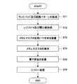
以下、本発明の回路基板の一例としての回路基板100の製造方法について説明する。
図5は、回路基板100の製造方法の一例を示すフローチャートである。
ステップST1:
回路基板100の表面全体にめっき等により銅や金等の金属層を形成し、この金属層をフォトリソグラフィ手法により所定の形状にパターニングすることにより導通ランドパッド11及び12、配線パターン13、14、15、実装ランドパッド21及び22、配線パターン23及び24等を含む回路パターンを形成する。
ステップST2:
回路基板100の表面全体にレジスト16を形成する。また、ここではレジスト16の開口部16a、16b、及び16cを形成する。なお、ステップST2は本発明のレジスト形成工程に対応している。Hereinafter, a method for manufacturing the
FIG. 5 is a flowchart showing an example of a method for manufacturing the
Step ST1:
A metal layer such as copper or gold is formed on the entire surface of the
Step ST2:
A resist 16 is formed on the entire surface of the
ステップST3:
メタルマスクを用いて回路基板100上の所定の位置に半田を配置(塗布)する。
本ステップST3が本発明の半田塗布工程に対応している。
メタルマスクとは、所定位置に所定の形状・所定の大きさの孔部が形成された金属板であり、回路基板100にかぶせて使用される。メタルマスクは、回路基板100にかぶせた場合、半田が配置されるべき箇所(導通ランドパッド11及び12、実装ランドパッド21及び22等)に孔部が位置する様になっており、メタルマスクをかぶせた状態でメタルマスクの上面に半田クリームを配置して、メタルマスクの上面に沿ってスキージを摺動させることにより、半田クリームをメタルマスクの孔部内に充填する。次にメタルマスクを回路基板100から離間させることにより、回路基板100の所定の位置に半田を配置させることができる。Step ST3:
Solder is placed (applied) at a predetermined position on the
This step ST3 corresponds to the solder application process of the present invention.
The metal mask is a metal plate in which a hole having a predetermined shape and a predetermined size is formed at a predetermined position, and is used by covering the
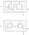
メタルマスクの具体例について説明する。
図6は、回路基板100上にかぶせるメタルマスク30の一例を示す図である。
図6(a)は、メタルマスク30の導通ランドパッド11及び12の上にかぶせられる部位の上面透視図であり、メタルマスク30が有する孔部31を説明するための図である。
図6に示すように、メタルマスク30の孔部31は、回路基板100の導通ランドパッド11に重なるように配置される。メタルマスク30により、導通ランドパッド11に半田が配置されることになる。メタルマスク30の孔部31が導通ランドパッド11の上に重なるように配置され、導通ランドパッド12の上には孔部が形成されない理由については後に説明する。A specific example of the metal mask will be described.
FIG. 6 is a diagram illustrating an example of the
FIG. 6A is a top perspective view of a portion of the
As shown in FIG. 6, the
また、メタルマスク30の孔部31は、メタルマスク30の他の孔部32とは形状を異ならせている。図6(b)は、導通ランドパッド以外のランドパッド、すなわち実装ランドパッド21及び22の上に重なるように配置される孔部32の形状について説明するためのメタルマスク30の上面透視図である。
図6(a)及び図6(b)に示すように、孔部31と孔部32とは形状が異なる。図6(a)及び図6(b)では、一例として、孔部31が三角形状、孔部32が円形状となっている。Further, the
As shown in FIGS. 6A and 6B, the
メタルマスク30の孔部31と孔部32の形状がそれぞれ異なる理由について説明する。
メタルマスク30の孔部31と孔部32との形状が異なることにより、回路基板100の導通ランドパッド11に配置される半田の形状と、実装ランドパッド21及び22に配置される半田の形状とがそれぞれ異なる。
このため、後の工程(ステップST5)においてメタルマスク30が除去され、電子部品が配置される(ステップST6)際に、導通ランドパッド11と実装ランドパッド21及び22とを容易に見分けることができるようになるため、電子部品の配置ミスの減少を期待できる。同時に、さらに後の工程(ステップST7)において、リフロー処理により半田付けがなされた後も、半田の形状が異なることにより導通ランドパッド11の位置を容易に見つけ出すことができるため、検査時に多くのランドパッドの中から検査ポイントとしての導通ランドパッド11(及び12)を見つけ出す労力を減少させることができる。The reason why the shapes of the
Due to the different shapes of the
For this reason, when the
なお、図6においては、孔部31を三角形状、孔部32を円形状としたが、本発明はこれには限定されず、孔部31と孔部32とが異なる形状であれば、他の形状でもよい。ただし、リフロー処理後にも導通ランドパッド11に配置された半田と実装ランドパッド21及び22に配置された半田の形状が異なっていることが望ましいため、半田が一度溶融し再度固まっても明らかに形状が異なることが判る程度には孔部31の形状と孔部32の形状とが異なっていることが望ましい。このため、例えば、孔部31と孔部32との形状を明らかに異ならせるだけでなく、孔の面積を異ならせる(例えば孔部31よりも孔部32のほうが明らかに大きい)等してもよい。 In FIG. 6, the
ステップST5:
ステップST4における半田(半田クリーム)の配置が済んだなら、回路基板100上からメタルマスク30を除去する。
ステップST6:
回路基板100上において、実装すべき電子部品を実装すべき位置に配置する。
回路基板100上には種々の電子部品が配置されるが、例えば、実装ランドパッド21と実装ランドパッド22との間には抵抗素子等が配置される。電子部品の配置は、例えばマウンタによって行われる。マウンタによって、電子部品が配置された位置にステップST4において配置された半田(クリーム)が、配置された電子部品によって潰される。Step ST5:
After the placement of the solder (solder cream) in step ST4, the
Step ST6:
On the
Various electronic components are arranged on the
ステップST7:
ステップST6における電子部品の配置が終了したなら、リフロー処理を行う。リフロー処理により、回路基板100上に配置された各電子部品が各実装ランドパッドに半田付けされ、電子部品が回路基板100に実装される。
なお、リフロー処理とは赤外線や熱風等により配置された半田クリームを溶融させて半田付けを行う処理である。
ステップST7は、本発明の実装工程に対応している。Step ST7:
When the arrangement of the electronic components in step ST6 is completed, reflow processing is performed. By the reflow process, each electronic component arranged on the
The reflow process is a process for performing soldering by melting a solder cream arranged by infrared rays or hot air.
Step ST7 corresponds to the mounting process of the present invention.
回路基板100の製造方法は上述した通りである。
以下、メタルマスク30の孔部31が導通ランドパッド11の上に重なるように配置され、導通ランドパッド12の上には孔部が形成されない理由について説明する。
回路基板100に電子部品が配置される際(ステップST6)、何らかのミスにより導通ランドパッド11と導通ランドパッド12との間に電子部品が配置されてしまうことがある。この場合、従来のように導通ランドパッド11及び導通ランドパッド12の両方に半田クリームが配置されていた場合には、導通ランドパッド11と導通ランドパッド12との間に誤って配置された電子部品が半田付けされ、実装されてしまうことになる。この場合には、回路基板100は回路全体で設計された通りの動作を行うことができなくなる場合があり、このようなミスは速やかに訂正されなければならないが、ミスにより導通ランドパッド11及び12に実装されてしまった電子部品を見つけ出し、電子部品を取り除くことは非常に難しく、手間がかかる、という不利益があった。
しかし、回路基板100のように、メタルマスク30の孔部31が導通ランドパッド11に重なる様に配置されることにより、半田が導通ランドパッド11にのみ配置されると、電子部品が導通ランドパッド11と導通ランドパッド12との間に誤って配置された場合にはマンハッタン現象が起きるため、電子部品の配置ミス箇所を容易に発見することができるようになる。The manufacturing method of the
Hereinafter, the reason why the
When an electronic component is arranged on the circuit board 100 (step ST6), the electronic component may be arranged between the
However, when the solder is disposed only on the
なお、マンハッタン現象とは、2つのランドパッド間に接続されるべき電子部品が、片方のランドパッドにしか半田付けされず、溶融した半田の表面張力等により立ち上がってしまい、そのまま固定されてしまう現象である。回路基板100においては、導通ランドパッド11には上述したように半田が配置され、導通ランドパッド12には半田が配置されないので、導通ランドパッド11と導通ランドパッド12との間に誤って電子部品が配置されてしまった場合でも、電子部品の片側のみ半田付けされるため、電子部品が立ち上がりマンハッタン現象が生じる。このため誤って配置された電子部品をリフロー工程(ステップST7)の後に容易に発見できる。 The Manhattan phenomenon is a phenomenon in which an electronic component to be connected between two land pads is soldered only to one land pad, rises due to the surface tension of the molten solder, and is fixed as it is. It is. In the
なお、上述した説明では、メタルマスク30には導通ランドパッド11の上にのみ孔部31が開いており、導通ランドパッド12の上には孔部が開いていないため、半田配置工程(ステップST3)において導通ランドパッド11にのみ半田が配置され、導通ランドパッド12には半田が配置されないとしたが、本発明はこれに限定されない。本発明には、上記の逆の場合、すなわち、導通ランドパッド11の上にはメタルマスク30の孔部が開いておらず、導通ランドパッド12の上に孔部31が開いており、導通ランドパッド11には半田が配置されず導通ランドパッド12にのみ半田が配置される場合も含まれる。
すなわち、本発明では、メタルマスク30には導通ランドパッド11及び12のいずれか一方の上にのみ孔部31が開いており、導通ランドパッド11及び12のいずれか一方の上にのみ半田が配置されるようになっている。
本発明では、導通ランドパッド11及び12のいずれか一方の上にのみ半田が配置されることにより、電子部品が誤って導通ランドパッド11と導通ランドパッド12との間に配置されてしまった場合でも、リフロー工程において意図的にマンハッタン現象を起こさせることができ、電子部品の配置ミスを発見しやすくすることが可能である。In the above description, since the
That is, in the present invention, the
In the present invention, when the solder is disposed only on one of the
以上説明したように、本発明の回路基板の一例としての回路基板100によれば、検査ポイントとして使用される導通ランドパッド11及び12とを配線パターン13により接続したため、従来のように0Ω抵抗素子を回路基板上に配置しておく必要がなくなり、0Ω抵抗素子の部品代を節約することができ、同時に0Ω抵抗素子の実装工程を省略することができるため、回路基板100の製造コストを従来と比較して抑えることができるとともに、導通ランドパッド11と導通ランドパッド12との間隔を他のランドパッド、例えば実装ランドパッド21と22と比較して狭めることができるので、導通ランドパッド11及び12のために必要な回路基板100上の面積を縮小することができ、回路基板100の基板面積を有効に活用することができるようになる。また、0Ω抵抗素子を実装する必要がないため回路基板100の歩留まりも向上する。 As described above, according to the
また、回路基板100によれば、配線パターン13上にレジスト開口部16cが開けられているために、回路基板100の検査時等に、検査ポイントとして使用される導通ランドパッド11及び12の位置を容易に見つけ出すことができるようになるとともに、配線パターン13を容易にカットすることができ、カット時のカットズレを抑えることが可能である。 Further, according to the
また、回路基板100によれば、メタルマスク30には導通ランドパッド11と導通ランドパッド12のいずれか一方の上に重なる部位にのみ孔部31が開けられているため、導通ランドパッド11と導通ランドパッド12のいずれか一方にのみ半田が配置され、電子部品が誤って導通ランドパッド11と導通ランドパッド12との間に配置されてしまった場合でも、マンハッタン現象を意図的に生じさせることができ、誤って配置された電子部品をリフロー処理後に容易に見つけ出すことができる。 Further, according to the
また、回路基板100によれば、メタルマスク30の導通ランドパッド11(或いは12)の上に重なる部位に開けられた孔部31と、導通ランドパッド以外のランドパッド、すなわち例えば実装ランドパッド21及び22の上に重なる部位に空けられた孔部32との形状が異なるため、導通ランドパッド11(或いは12)に配置される半田と実装ランドパッド21及び22に配置される半田との形状或いは面積が異なり、導通ランドパッド11(或いは12)と実装ランドパッド21及び22を容易に見分けることができるようになる。また、回路基板100の検査時等には、導通ランドパッド11(或いは12)を容易に見つけ出すことができるようになる。 Further, according to the
本発明は上述した実施形態には限定されない。
すなわち、本発明の実施に際しては、本発明の技術的範囲またはその均等の範囲内において、上述した実施形態の構成要素に関し様々な変更、コンビネーション、サブコンビネーション、並びに代替を行ってもよい。The present invention is not limited to the embodiment described above.
That is, when implementing the present invention, various modifications, combinations, sub-combinations, and alternatives may be made to the components of the above-described embodiments within the technical scope of the present invention or an equivalent scope thereof.
上述した実施形態の回路基板100では、図1に示すように、導通ランドパッド11及び12は、矩形状をしているとしたが、本発明はこれには限定されない。すなわち、導通ランドパッド11及び12は、例えば半長円形状等、他の形状をしていてもよい。図2に関連付けて説明した、実装ランドパッド21及び22に関しても同様である。
また、上述した実施形態の回路基板100では、回路基板100上に導通ランドパッド11及び12と実装ランドパッド21及び22の数については触れていないが、実際には多数の導通ランドパッド及び実装ランドパッドが形成されている。回路基板100上に形成された多数の導通ランドパッドが、全て上記実施形態において説明した導通ランドパッド11及び12と同様の特徴を有していてもよい。In the
Further, in the
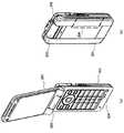
なお、上述した実施形態の回路基板100は、例えば図7に示す携帯電話機200に内蔵される。携帯電話機200は、本発明の携帯電子機器の一例である。
図7は、携帯電話機200の外観の一例を示す図である。
図7に示すように、携帯電話機200は、上部筐体201と下部筐体202とがヒンジ部203によって開閉可能に接続されている。
図7(a)は携帯電話機200の筐体が開かれた状態を、図7(b)は携帯電話機200の筐体が閉じられた状態を示している。
上部筐体201には、例えば有機EL(Electro-Luminescence)デバイスや液晶ディスプレイ(LCD:Liquid Crystal Display)等により構成された表示部やスピーカ等が配置されている。
下部筐体202には、通話キー、終話キー、テンキー等を含む操作部、音声通話用のマイクロフォンが配置され、携帯電話機200の各構成(すなわち回路基板100上の電子部品)に給電を行うバッテリ204(点線で図示)を内包している。
携帯電話機200は、図示しない基地局等と通信を行うことにより、音声通話、データ通信等を行うことが可能である。Note that the
FIG. 7 is a diagram showing an example of the appearance of the mobile phone 200.
As shown in FIG. 7, in the mobile phone 200, an
FIG. 7A shows a state where the casing of the mobile phone 200 is opened, and FIG. 7B shows a state where the casing of the mobile phone 200 is closed.
In the
The
The mobile phone 200 can perform a voice call, data communication, and the like by communicating with a base station (not shown).
なお、本発明の電子機器は、携帯電話機200に限定されず、例えばPDA(Personal Digital Assistants)、PHS(Personal Handyphone System)、PC(Personal Computer)等、電子回路を有し、回路基板を内蔵するような電子機器であればよい。 The electronic device of the present invention is not limited to the mobile phone 200, and includes an electronic circuit such as a PDA (Personal Digital Assistants), a PHS (Personal Handyphone System), a PC (Personal Computer), and the like, and includes a circuit board. Any electronic device may be used.
100…回路基板、11…導通ランドパッド、12…導通ランドパッド、13…配線パターン、14…配線パターン、15…配線パターン、16…レジスト、16a…開口部、16b…開口部、16c…開口部、21…実装ランドパッド、22…実装ランドパッド、23…配線パターン、24…配線パターン、30…メタルマスク、31…孔部、32…孔部、200…携帯電話機、201…上部筐体、202…下部筐体、203…ヒンジ部、204…バッテリ DESCRIPTION OF
Claims (7)
Translated fromJapanese前記配線パターンに接続される複数のランドパッドと、
前記ランドパッドを露出させる開口部を有し、基板表面に形成されたレジストと、
前記複数のランドパッドのうち少なくとも1つに実装される電子部品と、
を備える回路基板において、
前記複数のランドパッドは、前記電子部品が実装されず、かつ隣り合う第1導通ランドパッド及び第2導通ランドパッドを含み、
前記第1導通ランドパッドと前記第2導通ランドパッドとが互いに接続され、
前記第1導通ランドパッドと前記第2導通ランドパッドのうち、いずれか一方のみに半田が配されている
ことを特徴とする回路基板。A wiring pattern;
A plurality of land pads connected to the wiring pattern;
It has an opening that exposes the landpads, and resist formed on theboard surface,
An electronic component mounted on at least one of the plurality of land pads;
In a circuit board comprising:
The plurality of land pads include a first conductive land pad and a second conductive land pad that are not mounted with the electronic component and are adjacent to each other.
The first conductive land pad and the second conductive land pad are connected to each other;
A circuit board, wherein solder is disposed on only one of the first conductive land pad and the second conductive land pad .
前記第1導通ランドパッドと前記第2導通ランドパッドとの間隔は、前記第1実装ランドパッドと前記第2実装ランドパッドとの間隔よりも狭い
ことを特徴とする請求項1に記載の回路基板。The plurality of land pads include a first mounting land pad and a second mounting land pad that are arranged at predetermined intervals and on which the electronic component is mounted,
2. The circuit board according to claim 1, wherein an interval between the first conductive land pad and the second conductive land pad is narrower than an interval between the first mounting land pad and the second mounting land pad. .
ことを特徴とする請求項1または2に記載の回路基板。The opening portion of the resist is formed between the first conductive land pad and the second conductive land pad so as to expose the wiring patterns that connect each other. 2. The circuit board according to 2.
前記第1導通ランドパッドと前記第2導通ランドパッドのうち、少なくとも一方には半田が配されており、当該半田は、前記第1実装ランドパッド及び前記第2実装ランドパッドに配される半田とは外観形状が異なる
ことを特徴とする請求項1から3のいずれか一項に記載の回路基板。The plurality of land pads include a first mounting land pad and a second mounting land pad that are arranged at predetermined intervals and on which the electronic component is mounted,
At least one of the first conductive land pad and the second conductive land pad is provided with solder, and the solder is disposed on the first mounting land pad and the second mounting land pad. The circuit board according to any one of claims 1 to3 , wherein the external shapes are different.
前記電子部品に給電を行うバッテリと、
前記回路基板及びバッテリを内包する筐体と、
を有し、
前記回路基板は、
少なくとも前記配線パターンのうち、前記ランドパッドを露出させる開口部を有し、前記基板表面に形成されたレジスト
をさらに有し、
前記複数のランドパッドは、前記電子部品が実装されず、かつ隣り合う第1導通ランドパッド及び第2導通ランドパッドを含み、
前記第1導通ランドパッドと前記第2導通ランドパッドとが互いに接続され、
前記第1導通ランドパッドと前記第2導通ランドパッドのうち、いずれか一方のみに半田が配されている
ことを特徴とする携帯電子機器。A circuit board having a wiring pattern, a plurality of land pads connected to the wiring pattern, and an electronic component mounted on at least one of the plurality of land pads;
A battery for supplying power to the electronic component;
A housing containing the circuit board and the battery;
Have
The circuit board is
At least an opening for exposing the land pad of the wiring pattern, and further comprising a resist formed on the substrate surface;
The plurality of land pads include a first conductive land pad and a second conductive land pad that are not mounted with the electronic component and are adjacent to each other.
The first conductive land pad and the second conductive land pad are connected to each other;
A portable electronic device, wherein solder is disposed on only one of the first conductive land pad and the second conductive land pad .
前記複数のランドパッドのうち、互いに接続され、いずれか一方のみに半田が配されている第1導通ランドパッドと第2導通ランドパッドを除いて電子部品を実装する実装工程と、
を有することを特徴とする回路基板の製造方法。A resist formation step of forming a resist on the circuit board with a plurality of land pads, a wiring pattern that connects each of the plurality of land pads, and an opening that exposes the plurality of land pads;
A mounting step of mounting electronic components except for the first conductive land pad and the second conductive land pad which are connected to eachother and solder is disposed on only one of the plurality of land pads;
A method of manufacturing a circuit board, comprising:
前記半田塗布工程においては、前記複数のランドパッドのうち、前記第1導通ランドパッドと前記第2導通ランドパッドの少なくとも一方には、他のランドパッド用とは異なる孔形状を有するメタルマスクを用いて半田を塗布する
ことを特徴とする請求項6に記載の回路基板の製造方法。A solder application step of applying solder to the plurality of land pads;
In the solder application step, a metal mask having a hole shape different from that for other land pads is used for at least one of the first conductive land pads and the second conductive land pads among the plurality of land pads. The method for manufacturing a circuit board according to claim 6, wherein solder is applied.
Priority Applications (3)
| Application Number | Priority Date | Filing Date | Title |
|---|---|---|---|
| JP2007041755AJP4912917B2 (en) | 2007-02-22 | 2007-02-22 | Circuit board, portable electronic device, and circuit board manufacturing method |
| CN2008100814466ACN101252807B (en) | 2007-02-22 | 2008-02-22 | Circuit board and electronic equipment having the same, method of manufacturing same |
| US12/035,819US8116092B2 (en) | 2007-02-22 | 2008-02-22 | Circuit board and method of manufacturing same |
Applications Claiming Priority (1)
| Application Number | Priority Date | Filing Date | Title |
|---|---|---|---|
| JP2007041755AJP4912917B2 (en) | 2007-02-22 | 2007-02-22 | Circuit board, portable electronic device, and circuit board manufacturing method |
Publications (2)
| Publication Number | Publication Date |
|---|---|
| JP2008205335A JP2008205335A (en) | 2008-09-04 |
| JP4912917B2true JP4912917B2 (en) | 2012-04-11 |
Family
ID=39732912
Family Applications (1)
| Application Number | Title | Priority Date | Filing Date |
|---|---|---|---|
| JP2007041755AExpired - Fee RelatedJP4912917B2 (en) | 2007-02-22 | 2007-02-22 | Circuit board, portable electronic device, and circuit board manufacturing method |
Country Status (3)
| Country | Link |
|---|---|
| US (1) | US8116092B2 (en) |
| JP (1) | JP4912917B2 (en) |
| CN (1) | CN101252807B (en) |
Families Citing this family (6)
| Publication number | Priority date | Publication date | Assignee | Title |
|---|---|---|---|---|
| CN104080270A (en)* | 2013-03-25 | 2014-10-01 | 飞思卡尔半导体公司 | Separation pad for circuit board |
| US9806005B2 (en)* | 2014-04-23 | 2017-10-31 | Kyocera Corporation | Electronic element mounting substrate and electronic device |
| TWI620475B (en)* | 2015-01-12 | 2018-04-01 | 南亞電路板股份有限公司 | Printed circuit board and method for fabricating the same |
| US11852630B2 (en)* | 2015-10-16 | 2023-12-26 | Toyobo Co., Ltd. | Immunochromatographic test piece |
| JP6834979B2 (en)* | 2015-12-02 | 2021-02-24 | 東洋紡株式会社 | Immunochromatographic test piece |
| CN110610932A (en)* | 2019-08-27 | 2019-12-24 | 华东光电集成器件研究所 | A method for preventing the breakage of the thick-film integrated circuit conductive tape |
Family Cites Families (21)
| Publication number | Priority date | Publication date | Assignee | Title |
|---|---|---|---|---|
| US4254445A (en)* | 1979-05-07 | 1981-03-03 | International Business Machines Corporation | Discretionary fly wire chip interconnection |
| US4414741A (en)* | 1981-05-22 | 1983-11-15 | Augat Inc. | Process for interconnecting components on a PCB |
| JPS624165A (en)* | 1985-06-27 | 1987-01-10 | Shinko Electric Co Ltd | Tension control method for winder or rewinder |
| JPH03120065A (en)* | 1989-10-03 | 1991-05-22 | Oki Electric Ind Co Ltd | Printer |
| JP2818911B2 (en)* | 1991-03-20 | 1998-10-30 | イビデン株式会社 | Printed wiring board |
| JPH0563327A (en)* | 1991-09-04 | 1993-03-12 | Canon Inc | Printed wiring board with land for inspection use and inspecting method thereof |
| JPH0786729A (en)* | 1993-09-09 | 1995-03-31 | Ibiden Co Ltd | Connection structure of jumper land in printed-wiring board and connection of jumper land |
| US5877033A (en)* | 1997-03-10 | 1999-03-02 | The Foxboro Company | System for detection of unsoldered components |
| JP4423630B2 (en)* | 2000-08-03 | 2010-03-03 | ミネベア株式会社 | Microchip controller board and manufacturing method thereof |
| JP2002280693A (en)* | 2001-03-19 | 2002-09-27 | Denso Corp | Method for mounting electronic part |
| JP3692314B2 (en)* | 2001-07-17 | 2005-09-07 | 日東電工株式会社 | Printed circuit board |
| JP2003163430A (en)* | 2001-11-27 | 2003-06-06 | Nec Corp | Printed board |
| JP2003168501A (en) | 2001-11-29 | 2003-06-13 | Toko Inc | Jumper chip and its manufacturing method |
| SG121707A1 (en)* | 2002-03-04 | 2006-05-26 | Micron Technology Inc | Method and apparatus for flip-chip packaging providing testing capability |
| TW564533B (en)* | 2002-10-08 | 2003-12-01 | Siliconware Precision Industries Co Ltd | Warpage-preventing substrate |
| JP2005032815A (en)* | 2003-07-08 | 2005-02-03 | Alps Electric Co Ltd | Flexible wiring board and its manufacturing method |
| JP2006005151A (en)* | 2004-06-17 | 2006-01-05 | Casio Comput Co Ltd | Flexible printed wiring board and its ground connection structure |
| DE102004050967A1 (en)* | 2004-10-15 | 2006-04-20 | Hainbuch Gmbh Spannende Technik | Clamping device and method for producing a clamping device |
| US7388394B1 (en)* | 2004-12-01 | 2008-06-17 | Cardiac Pacemakers, Inc. | Multiple layer printed circuit board having misregistration testing pattern |
| AT501513B1 (en)* | 2005-03-01 | 2007-06-15 | Austria Tech & System Tech | MULTILAYER CIRCUIT BOARD WITH CONDUCTIVE TEST SURFACES AND METHOD FOR DETERMINING AN INSERT OF AN INSIDE SITUATION |
| JP2007067019A (en)* | 2005-08-29 | 2007-03-15 | Kyocera Corp | Circuit board, electronic device, and circuit board manufacturing method |
- 2007
- 2007-02-22JPJP2007041755Apatent/JP4912917B2/ennot_activeExpired - Fee Related
- 2008
- 2008-02-22USUS12/035,819patent/US8116092B2/ennot_activeExpired - Fee Related
- 2008-02-22CNCN2008100814466Apatent/CN101252807B/ennot_activeExpired - Fee Related
Also Published As
| Publication number | Publication date |
|---|---|
| US8116092B2 (en) | 2012-02-14 |
| JP2008205335A (en) | 2008-09-04 |
| CN101252807B (en) | 2011-02-02 |
| US20080212300A1 (en) | 2008-09-04 |
| CN101252807A (en) | 2008-08-27 |
Similar Documents
| Publication | Publication Date | Title |
|---|---|---|
| JP2007067019A (en) | Circuit board, electronic device, and circuit board manufacturing method | |
| US7506437B2 (en) | Printed circuit board having chip package mounted thereon and method of fabricating same | |
| JP4912917B2 (en) | Circuit board, portable electronic device, and circuit board manufacturing method | |
| US7660129B2 (en) | Printed circuit board, solder connection structure and method between printed circuit board and flexible printed circuit board | |
| US5834705A (en) | Arrangement for modifying eletrical printed circuit boards | |
| CN101568224A (en) | Circuit board and electronic device having circuit board | |
| EP2086296B1 (en) | Printed circuit board and method of manufacturing the same | |
| JP2011086838A (en) | Electronic apparatus, and method of mounting circuit board used for the same | |
| US8243462B2 (en) | Printed wiring board, semiconductor device, and method for manufacturing printed wiring board | |
| KR101068539B1 (en) | Method for manufacturing wiring board using electrolytic plating | |
| KR20130055990A (en) | Rigid-flexible printed circuit board and method for manufacturing the same | |
| WO2021043161A1 (en) | Circuit board and electronic device | |
| JP6834775B2 (en) | How to solder boards, electronic devices and electronic components to which electronic components are soldered | |
| US8832932B2 (en) | Method of mounting an electronic component on a circuit board | |
| JP6295598B2 (en) | Printed circuit board manufacturing method and printed circuit board unit manufacturing method | |
| JP5059220B2 (en) | Circuit board | |
| JP2003249743A (en) | Wiring board and method of manufacturing the same, semiconductor device and electronic equipment | |
| CN100531514C (en) | Short-proof printed circuit board structure | |
| JP2001308491A (en) | Single-sided circuit board, display module having the same and method for connecting the same | |
| CN101442875A (en) | Circuit board with multi-layer solder mask structure | |
| KR100785975B1 (en) | Tape wiring board connected with test wiring and inspection method | |
| KR100584142B1 (en) | Wall printed circuit board and chipset device for mobile terminal | |
| CN115980415A (en) | Manufacturing method of conduction test module and conduction test module | |
| KR20070069546A (en) | Printed Circuit Board Structure with Debugging Pattern of Communication Terminal | |
| KR20250118160A (en) | Printed circuit board |
Legal Events
| Date | Code | Title | Description |
|---|---|---|---|
| A621 | Written request for application examination | Free format text:JAPANESE INTERMEDIATE CODE: A621 Effective date:20100212 | |
| A977 | Report on retrieval | Free format text:JAPANESE INTERMEDIATE CODE: A971007 Effective date:20110928 | |
| A131 | Notification of reasons for refusal | Free format text:JAPANESE INTERMEDIATE CODE: A131 Effective date:20111011 | |
| A521 | Request for written amendment filed | Free format text:JAPANESE INTERMEDIATE CODE: A523 Effective date:20111209 | |
| TRDD | Decision of grant or rejection written | ||
| A01 | Written decision to grant a patent or to grant a registration (utility model) | Free format text:JAPANESE INTERMEDIATE CODE: A01 Effective date:20111227 | |
| A01 | Written decision to grant a patent or to grant a registration (utility model) | Free format text:JAPANESE INTERMEDIATE CODE: A01 | |
| A61 | First payment of annual fees (during grant procedure) | Free format text:JAPANESE INTERMEDIATE CODE: A61 Effective date:20120118 | |
| R150 | Certificate of patent or registration of utility model | Ref document number:4912917 Country of ref document:JP Free format text:JAPANESE INTERMEDIATE CODE: R150 Free format text:JAPANESE INTERMEDIATE CODE: R150 | |
| FPAY | Renewal fee payment (event date is renewal date of database) | Free format text:PAYMENT UNTIL: 20150127 Year of fee payment:3 | |
| LAPS | Cancellation because of no payment of annual fees |