JP4907984B2 - Laser processing method and semiconductor chip - Google Patents
Laser processing method and semiconductor chipDownload PDFInfo
- Publication number
- JP4907984B2 JP4907984B2JP2005375695AJP2005375695AJP4907984B2JP 4907984 B2JP4907984 B2JP 4907984B2JP 2005375695 AJP2005375695 AJP 2005375695AJP 2005375695 AJP2005375695 AJP 2005375695AJP 4907984 B2JP4907984 B2JP 4907984B2
- Authority
- JP
- Japan
- Prior art keywords
- substrate
- region
- modified region
- modified
- line
- Prior art date
- Legal status (The legal status is an assumption and is not a legal conclusion. Google has not performed a legal analysis and makes no representation as to the accuracy of the status listed.)
- Active
Links
- 238000003672processing methodMethods0.000titleclaimsdescription69
- 239000004065semiconductorSubstances0.000titleclaimsdescription25
- 239000000758substrateSubstances0.000claimsdescription150
- 238000005520cutting processMethods0.000claimsdescription134
- 230000015572biosynthetic processEffects0.000claimsdescription69
- 238000012545processingMethods0.000claimsdescription45
- 238000010128melt processingMethods0.000claimsdescription31
- 230000004048modificationEffects0.000claimsdescription11
- 238000012986modificationMethods0.000claimsdescription11
- 230000001678irradiating effectEffects0.000claimsdescription7
- 238000002407reformingMethods0.000description56
- XUIMIQQOPSSXEZ-UHFFFAOYSA-NSiliconChemical compound[Si]XUIMIQQOPSSXEZ-UHFFFAOYSA-N0.000description52
- 229910052710siliconInorganic materials0.000description51
- 239000010703siliconSubstances0.000description51
- 238000010521absorption reactionMethods0.000description28
- 238000000034methodMethods0.000description15
- 239000013078crystalSubstances0.000description14
- 230000005684electric fieldEffects0.000description12
- 230000008569processEffects0.000description10
- 239000011229interlayerSubstances0.000description8
- 239000010410layerSubstances0.000description7
- 230000001681protective effectEffects0.000description7
- 238000002834transmittanceMethods0.000description6
- 230000008859changeEffects0.000description5
- 239000011521glassSubstances0.000description5
- 239000000463materialSubstances0.000description5
- 238000002474experimental methodMethods0.000description4
- 238000002844meltingMethods0.000description4
- 230000008018meltingEffects0.000description4
- 230000003287optical effectEffects0.000description4
- 238000003776cleavage reactionMethods0.000description3
- 238000005336crackingMethods0.000description3
- 238000009826distributionMethods0.000description3
- 230000004927fusionEffects0.000description3
- 239000000155meltSubstances0.000description3
- 238000010309melting processMethods0.000description3
- 230000010287polarizationEffects0.000description3
- 230000007017scissionEffects0.000description3
- 230000035882stressEffects0.000description3
- 230000006866deteriorationEffects0.000description2
- 238000010438heat treatmentMethods0.000description2
- 238000003475laminationMethods0.000description2
- 230000010355oscillationEffects0.000description2
- 230000000149penetrating effectEffects0.000description2
- 230000002093peripheral effectEffects0.000description2
- 238000011160researchMethods0.000description2
- RZVAJINKPMORJF-UHFFFAOYSA-NAcetaminophenChemical compoundCC(=O)NC1=CC=C(O)C=C1RZVAJINKPMORJF-UHFFFAOYSA-N0.000description1
- 229910001218Gallium arsenideInorganic materials0.000description1
- 239000000853adhesiveSubstances0.000description1
- 230000001070adhesive effectEffects0.000description1
- 230000004075alterationEffects0.000description1
- 229910021417amorphous siliconInorganic materials0.000description1
- 238000005452bendingMethods0.000description1
- 150000001875compoundsChemical class0.000description1
- 238000002425crystallisationMethods0.000description1
- 230000008025crystallizationEffects0.000description1
- 230000003247decreasing effectEffects0.000description1
- 229910003460diamondInorganic materials0.000description1
- 239000010432diamondSubstances0.000description1
- 239000000428dustSubstances0.000description1
- 238000005516engineering processMethods0.000description1
- 238000011156evaluationMethods0.000description1
- 230000005284excitationEffects0.000description1
- 230000006872improvementEffects0.000description1
- 230000031700light absorptionEffects0.000description1
- 239000011159matrix materialSubstances0.000description1
- 230000007246mechanismEffects0.000description1
- 229910021421monocrystalline siliconInorganic materials0.000description1
- TWNQGVIAIRXVLR-UHFFFAOYSA-Noxo(oxoalumanyloxy)alumaneChemical compoundO=[Al]O[Al]=OTWNQGVIAIRXVLR-UHFFFAOYSA-N0.000description1
- 230000035699permeabilityEffects0.000description1
- 238000003825pressingMethods0.000description1
- 239000005297pyrexSubstances0.000description1
- 230000008646thermal stressEffects0.000description1
- 238000003466weldingMethods0.000description1
Images


Classifications
- H—ELECTRICITY
- H01—ELECTRIC ELEMENTS
- H01L—SEMICONDUCTOR DEVICES NOT COVERED BY CLASS H10
- H01L21/00—Processes or apparatus adapted for the manufacture or treatment of semiconductor or solid state devices or of parts thereof
- H01L21/02—Manufacture or treatment of semiconductor devices or of parts thereof
- H01L21/04—Manufacture or treatment of semiconductor devices or of parts thereof the devices having potential barriers, e.g. a PN junction, depletion layer or carrier concentration layer
- H01L21/18—Manufacture or treatment of semiconductor devices or of parts thereof the devices having potential barriers, e.g. a PN junction, depletion layer or carrier concentration layer the devices having semiconductor bodies comprising elements of Group IV of the Periodic Table or AIIIBV compounds with or without impurities, e.g. doping materials
- H01L21/30—Treatment of semiconductor bodies using processes or apparatus not provided for in groups H01L21/20 - H01L21/26
- B—PERFORMING OPERATIONS; TRANSPORTING
- B23—MACHINE TOOLS; METAL-WORKING NOT OTHERWISE PROVIDED FOR
- B23K—SOLDERING OR UNSOLDERING; WELDING; CLADDING OR PLATING BY SOLDERING OR WELDING; CUTTING BY APPLYING HEAT LOCALLY, e.g. FLAME CUTTING; WORKING BY LASER BEAM
- B23K26/00—Working by laser beam, e.g. welding, cutting or boring
- B23K26/36—Removing material
- B23K26/40—Removing material taking account of the properties of the material involved
- H—ELECTRICITY
- H01—ELECTRIC ELEMENTS
- H01L—SEMICONDUCTOR DEVICES NOT COVERED BY CLASS H10
- H01L23/00—Details of semiconductor or other solid state devices
- H01L23/544—Marks applied to semiconductor devices or parts, e.g. registration marks, alignment structures, wafer maps
- B—PERFORMING OPERATIONS; TRANSPORTING
- B23—MACHINE TOOLS; METAL-WORKING NOT OTHERWISE PROVIDED FOR
- B23K—SOLDERING OR UNSOLDERING; WELDING; CLADDING OR PLATING BY SOLDERING OR WELDING; CUTTING BY APPLYING HEAT LOCALLY, e.g. FLAME CUTTING; WORKING BY LASER BEAM
- B23K26/00—Working by laser beam, e.g. welding, cutting or boring
- B23K26/352—Working by laser beam, e.g. welding, cutting or boring for surface treatment
- B23K26/359—Working by laser beam, e.g. welding, cutting or boring for surface treatment by providing a line or line pattern, e.g. a dotted break initiation line
- B—PERFORMING OPERATIONS; TRANSPORTING
- B23—MACHINE TOOLS; METAL-WORKING NOT OTHERWISE PROVIDED FOR
- B23K—SOLDERING OR UNSOLDERING; WELDING; CLADDING OR PLATING BY SOLDERING OR WELDING; CUTTING BY APPLYING HEAT LOCALLY, e.g. FLAME CUTTING; WORKING BY LASER BEAM
- B23K26/00—Working by laser beam, e.g. welding, cutting or boring
- B23K26/50—Working by transmitting the laser beam through or within the workpiece
- B23K26/53—Working by transmitting the laser beam through or within the workpiece for modifying or reforming the material inside the workpiece, e.g. for producing break initiation cracks
- B—PERFORMING OPERATIONS; TRANSPORTING
- B28—WORKING CEMENT, CLAY, OR STONE
- B28D—WORKING STONE OR STONE-LIKE MATERIALS
- B28D5/00—Fine working of gems, jewels, crystals, e.g. of semiconductor material; apparatus or devices therefor
- B28D5/0005—Fine working of gems, jewels, crystals, e.g. of semiconductor material; apparatus or devices therefor by breaking, e.g. dicing
- B28D5/0011—Fine working of gems, jewels, crystals, e.g. of semiconductor material; apparatus or devices therefor by breaking, e.g. dicing with preliminary treatment, e.g. weakening by scoring
- C—CHEMISTRY; METALLURGY
- C03—GLASS; MINERAL OR SLAG WOOL
- C03B—MANUFACTURE, SHAPING, OR SUPPLEMENTARY PROCESSES
- C03B33/00—Severing cooled glass
- C03B33/02—Cutting or splitting sheet glass or ribbons; Apparatus or machines therefor
- C03B33/0222—Scoring using a focussed radiation beam, e.g. laser
- B—PERFORMING OPERATIONS; TRANSPORTING
- B23—MACHINE TOOLS; METAL-WORKING NOT OTHERWISE PROVIDED FOR
- B23K—SOLDERING OR UNSOLDERING; WELDING; CLADDING OR PLATING BY SOLDERING OR WELDING; CUTTING BY APPLYING HEAT LOCALLY, e.g. FLAME CUTTING; WORKING BY LASER BEAM
- B23K2101/00—Articles made by soldering, welding or cutting
- B23K2101/36—Electric or electronic devices
- B23K2101/40—Semiconductor devices
- B—PERFORMING OPERATIONS; TRANSPORTING
- B23—MACHINE TOOLS; METAL-WORKING NOT OTHERWISE PROVIDED FOR
- B23K—SOLDERING OR UNSOLDERING; WELDING; CLADDING OR PLATING BY SOLDERING OR WELDING; CUTTING BY APPLYING HEAT LOCALLY, e.g. FLAME CUTTING; WORKING BY LASER BEAM
- B23K2103/00—Materials to be soldered, welded or cut
- B23K2103/50—Inorganic material, e.g. metals, not provided for in B23K2103/02 – B23K2103/26
- H—ELECTRICITY
- H01—ELECTRIC ELEMENTS
- H01L—SEMICONDUCTOR DEVICES NOT COVERED BY CLASS H10
- H01L2924/00—Indexing scheme for arrangements or methods for connecting or disconnecting semiconductor or solid-state bodies as covered by H01L24/00
- H01L2924/0001—Technical content checked by a classifier
- H01L2924/0002—Not covered by any one of groups H01L24/00, H01L24/00 and H01L2224/00
Landscapes
- Engineering & Computer Science (AREA)
- Physics & Mathematics (AREA)
- Mechanical Engineering (AREA)
- Optics & Photonics (AREA)
- Chemical & Material Sciences (AREA)
- Plasma & Fusion (AREA)
- General Physics & Mathematics (AREA)
- Computer Hardware Design (AREA)
- Microelectronics & Electronic Packaging (AREA)
- Power Engineering (AREA)
- Condensed Matter Physics & Semiconductors (AREA)
- General Chemical & Material Sciences (AREA)
- Chemical Kinetics & Catalysis (AREA)
- Oil, Petroleum & Natural Gas (AREA)
- Organic Chemistry (AREA)
- Materials Engineering (AREA)
- Manufacturing & Machinery (AREA)
- Laser Beam Processing (AREA)
- Dicing (AREA)
- Processing Of Stones Or Stones Resemblance Materials (AREA)
Description
Translated fromJapanese本発明は、基板と、基板の表面に形成された複数の機能素子とを備える加工対象物を切断予定ラインに沿って切断するために使用されるレーザ加工方法、及びそのようなレーザ加工方法の使用により切断された半導体チップに関する。 The present invention relates to a laser processing method used for cutting a workpiece including a substrate and a plurality of functional elements formed on the surface of the substrate along a planned cutting line, and a method of such a laser processing method. The present invention relates to a semiconductor chip cut by use.
従来におけるこの種の技術として、ウェハ状の加工対象物の内部に集光点を合わせてレーザ光を照射することで、切断予定ラインに沿った改質領域を加工対象物の内部に複数列形成し、その改質領域を切断の起点とするというレーザ加工方法がある(例えば、特許文献1参照)。
上述したようなレーザ加工方法は、加工対象物が厚い場合に特に有効となる技術である。それは、加工対象物が厚い場合でも、切断予定ラインに沿った改質領域の列数を増やすことによって、加工対象物を切断予定ラインに沿って精度良く切断することができるからである。そして、このような技術に関しては、切断品質を維持した上での加工時間の短時間化が望まれている。 The laser processing method as described above is a technique that is particularly effective when a workpiece is thick. This is because even if the workpiece is thick, the workpiece can be cut along the scheduled cutting line with high accuracy by increasing the number of columns of the modified region along the scheduled cutting line. With regard to such a technique, it is desired to shorten the processing time while maintaining the cutting quality.
そこで、本発明は、このような事情に鑑みてなされたものであり、基板と、基板の表面に形成された複数の機能素子とを備える加工対象物を、その基板が厚い場合であっても、切断予定ラインに沿って短時間で精度良く切断することを可能にするレーザ加工方法、及びそのようなレーザ加工方法の使用により切断された半導体チップを提供することを目的とする。 Therefore, the present invention has been made in view of such circumstances, and a processing object including a substrate and a plurality of functional elements formed on the surface of the substrate can be processed even when the substrate is thick. An object of the present invention is to provide a laser processing method that enables high-accuracy cutting along a scheduled cutting line in a short time and a semiconductor chip cut by using such a laser processing method.
上記目的を達成するために、本発明に係るレーザ加工方法は、基板と、基板の表面に形成された複数の機能素子とを備える加工対象物の基板の内部に集光点を合わせてレーザ光を照射することにより、加工対象物の切断予定ラインに沿って、切断の起点となる改質領域を基板の内部に形成するレーザ加工方法であって、1本の切断予定ラインに対して、少なくとも1列の第1の改質領域、第1の改質領域と基板の表面との間に位置する少なくとも1列の第2の改質領域、及び第1の改質領域と基板の裏面との間に位置する少なくとも1列の第3の改質領域を形成する工程を含み、切断予定ラインに沿った方向に延在する1列当たりの第1の改質領域の形成密度は、切断予定ラインに沿った方向に延在する1列当たりの第2の改質領域の形成密度、及び切断予定ラインに沿った方向に延在する1列当たりの第3の改質領域の形成密度より低いことを特徴とする。In order to achieve the above object, a laser processing method according to the present invention includes a laser beam by aligning a condensing point inside a substrate of a processing target including a substrate and a plurality of functional elements formed on the surface of the substrate. Is a laser processing method for forming a modified region, which is a starting point of cutting, along the scheduled cutting line of the workpiece, inside the substrate, and at least with respect to one scheduled cutting line, A row of first modified regions, at least one row of second modified regions located between the first modified region and the surface of the substrate, and the first modified region and the back surface of the substrate. Forming a third modified region in at least one row located between the first modified regionsper row extending in a direction along the planned cutting line, second forming dense modifiedregions per row extending in a direction along the, And wherein the lower formation density of the third modified regionof 1 per row extending in a direction along the line to cut.
このレーザ加工方法では、切断予定ラインに沿った方向における第1の改質領域の形成密度を、切断予定ラインに沿った方向における第2の改質領域の形成密度及び第3の改質領域の形成密度より低くする。そのため、当該第1の改質領域の形成密度を当該第2の改質領域の形成密度及び当該第3の改質領域の形成密度と同等にする場合に比べ、第1、第2及び第3の改質領域の形成時間の短時間化を図ることできる。ところで、第1の改質領域と基板の表面との間に位置する第2の改質領域、及び第1の改質領域と基板の裏面との間に位置する第3の改質領域は、第1の改質領域に比べ、加工対象物の切断品質に大きな影響を与える。しかしながら、切断予定ラインに沿った方向における第2の改質領域の形成密度及び第3の改質領域の形成密度を、切断予定ラインに沿った方向における第1の改質領域の形成密度より高くするため、加工対象物の切断品質の劣化を防止することができる。以上により、このレーザ加工方法は、基板と、基板の表面に形成された複数の機能素子とを備える加工対象物を、その基板が厚い場合であっても、切断予定ラインに沿って短時間で精度良く切断することを可能にする。 In this laser processing method, the formation density of the first modified region in the direction along the planned cutting line is set to the formation density of the second modified region and the third modified region in the direction along the planned cutting line. Lower than the formation density. Therefore, compared with the case where the formation density of the first modified region is equal to the formation density of the second modified region and the formation density of the third modified region, the first, second and third It is possible to shorten the formation time of the modified region. By the way, the second modified region located between the first modified region and the front surface of the substrate, and the third modified region located between the first modified region and the back surface of the substrate, Compared to the first modified region, the cutting quality of the workpiece is greatly affected. However, the formation density of the second modified region and the formation density of the third modified region in the direction along the planned cutting line are higher than the formation density of the first modified region in the direction along the planned cutting line. Therefore, it is possible to prevent deterioration of the cutting quality of the workpiece. As described above, in this laser processing method, an object to be processed including a substrate and a plurality of functional elements formed on the surface of the substrate can be obtained in a short time along the planned cutting line even when the substrate is thick. It enables cutting with high accuracy.
ここで、機能素子とは、例えば、結晶成長により形成された半導体動作層、フォトダイオード等の受光素子、レーザダイオード等の発光素子、回路として形成された回路素子等を意味する。また、切断予定ラインに沿った方向に延在する1列当たりの改質領域の形成密度(以下、単に「改質領域の形成密度」という)とは、切断予定ラインに沿った方向に延在する1列の改質領域が、切断予定ラインに沿った方向の単位長さに分布する割合を意味する。Here, the functional element means, for example, a semiconductor operation layer formed by crystal growth, a light receiving element such as a photodiode, a light emitting element such as a laser diode, a circuit element formed as a circuit, and the like. Further, the formation densityof the modified regionper row extending in the direction along the planned cutting line (hereinafter simply referred to as “modified density of the modified region”) isthe direction extending along the planned cutting line. one row of modified regions to have meanspercentage you distribution unit length in the direction along the line to cut.
なお、第1、第2及び第3の改質領域のそれぞれを形成する順序は順不同である。また、第1、第2及び第3の改質領域は、基板の内部に集光点を合わせてレーザ光を照射して基板の内部で多光子吸収或いは他の光吸収を生じさせることにより形成される。 Note that the order of forming each of the first, second, and third modified regions is in no particular order. In addition, the first, second, and third modified regions are formed by aligning a condensing point inside the substrate and irradiating a laser beam to cause multiphoton absorption or other light absorption inside the substrate. Is done.
また、上記レーザ加工方法においては、基板の裏面をレーザ光入射面として基板の内部に集光点を合わせてレーザ光を照射する場合には、第2の改質領域の表面側端部と基板の表面との距離が5μm〜20μmとなるように第2の改質領域を形成することが好ましい。このように第2の改質領域が形成されていると、例えば、基板の表面の切断予定ライン上に積層部が形成されていても、その積層部を基板と共に切断予定ラインに沿って精度良く切断することが可能になる。 In the above laser processing method, when the back surface of the substrate is used as the laser beam incident surface and the laser beam is irradiated with the light converging point inside the substrate, the surface side end of the second modified region and the substrate It is preferable to form the second modified region so that the distance from the surface becomes 5 μm to 20 μm. When the second modified region is formed in this manner, for example, even if a stacked portion is formed on the planned cutting line on the surface of the substrate, the stacked portion is accurately aligned with the substrate along the planned cutting line. It becomes possible to cut.
また、上記レーザ加工方法においては、切断予定ラインに沿った割れが第3の改質領域から基板の裏面に生じるように第3の改質領域を形成することが好ましい。このように第3の改質領域が形成されていると、例えば、エキスパンドテープを基板の裏面に貼り付けて拡張させた場合に、第3の改質領域から基板の裏面に生じていた割れが、第1及び第2の改質領域を介して基板の表面に向かってスムーズに進行することになり、その結果、加工対象物を切断予定ラインに沿って精度良く切断することが可能になる。 Moreover, in the said laser processing method, it is preferable to form the 3rd modification area | region so that the crack along a cutting plan line may arise in the back surface of a board | substrate from a 3rd modification area | region. When the third modified region is formed in this way, for example, when the expanded tape is attached to the back surface of the substrate and expanded, cracks that have occurred from the third modified region to the back surface of the substrate are generated. Then, it proceeds smoothly toward the surface of the substrate through the first and second modified regions, and as a result, the workpiece can be cut along the planned cutting line with high accuracy.
また、上記レーザ加工方法においては、基板は半導体基板であり、第1、第2及び第3の改質領域は溶融処理領域を含む場合がある。基板が半導体基板であると、第1、第2及び第3の改質領域として、溶融処理領域を含む改質領域が形成される場合がある。 In the laser processing method, the substrate may be a semiconductor substrate, and the first, second, and third modified regions may include a melt processing region. When the substrate is a semiconductor substrate, a modified region including a melt processing region may be formed as the first, second, and third modified regions.
また、上記レーザ加工方法は、加工対象物を切断予定ラインに沿って機能素子毎に切断する工程を更に含んでもよい。上述した理由から、基板が厚い場合であっても、切断予定ラインに沿って短時間で精度良く加工対象物を機能素子毎に切断することができる。 In addition, the laser processing method may further include a step of cutting the processing object for each functional element along a planned cutting line. For the reasons described above, even if the substrate is thick, the workpiece can be cut for each functional element with high accuracy in a short time along the planned cutting line.
また、本発明に係るレーザ加工方法は、基板と、基板の表面に形成された複数の機能素子とを備える加工対象物の基板の内部に集光点を合わせてレーザ光を照射することにより、加工対象物の切断予定ラインに沿って、切断の起点となる改質領域を基板の内部に形成するレーザ加工方法であって、1本の切断予定ラインに対して、少なくとも1列の第1の改質領域、第1の改質領域と基板の表面との間に位置する少なくとも1列の第2の改質領域、及び第1の改質領域と基板の裏面との間に位置する少なくとも1列の第3の改質領域を形成する工程を含み、切断予定ラインに沿った方向に延在する1列の第1の改質領域を形成する際に切断予定ラインに沿ってレーザ光を加工対象物に対して相対移動させる速度は、切断予定ラインに沿った方向に延在する1列の第2の改質領域を形成する際、及び切断予定ラインに沿った方向に延在する1列の第3の改質領域を形成する際に切断予定ラインに沿ってレーザ光を加工対象物に対して相対移動させる速度より速いことを特徴とする。Further, the laser processing method according to the present invention irradiates a laser beam with a condensing point inside the substrate of the processing target including the substrate and a plurality of functional elements formed on the surface of the substrate, A laser processing method for forming, within a substrate, a modified region that is a starting point of cutting along a planned cutting line of an object to be processed, wherein at least one row of first lines is formed with respect to one scheduled cutting line. A modified region, at least one row of second modified regions located between the first modified region and the surface of the substrate, and at least one located between the first modified region and the back surface of the substrate. Forming a third modified region of therow, and processing the laser light along the planned cutting line when forming the first modified region ofone row extending in the direction along the planned cutting line speed to move relative to the object,person along the line to cut When formingthe second modified regionin one rowextending, and along the line to cut when forming the third modified regionin one row extending in a direction along the line to cut It is characterized by being faster than the speed at which the laser light is moved relative to the workpiece.
このレーザ加工方法によれば、第1の改質領域の形成密度を、第2の改質領域の形成密度及び第3の改質領域の形成密度より低くすることができる。従って、このレーザ加工方法は、上記レーザ加工方法と同様に、基板と、基板の表面に形成された複数の機能素子とを備える加工対象物を、その基板が厚い場合であっても、切断予定ラインに沿って短時間で精度良く切断することを可能にする。 According to this laser processing method, the formation density of the first modified region can be made lower than the formation density of the second modified region and the formation density of the third modified region. Therefore, this laser processing method, like the above laser processing method, is intended to cut a processing object including a substrate and a plurality of functional elements formed on the surface of the substrate, even if the substrate is thick. It is possible to cut along the line with high accuracy in a short time.
更に、本発明に係る半導体チップは、基板と、基板の表面に形成された機能素子とを備える半導体チップであって、基板の側面には、少なくとも1列の第1の改質領域、第1の改質領域と基板の表面との間に位置する少なくとも1列の第2の改質領域、及び第1の改質領域と基板の裏面との間に位置する少なくとも1列の第3の改質領域が形成されており、基板の厚さ方向と直交する方向に延在する1列当たりの第1の改質領域の形成密度は、基板の厚さ方向と直交する方向に延在する1列当たりの第2の改質領域の形成密度、及び基板の厚さ方向と直交する方向に延在する1列当たりの第3の改質領域の形成密度より低いことを特徴とする。Furthermore, a semiconductor chip according to the present invention is a semiconductor chip including a substrate and a functional element formed on the surface of the substrate, and at least one row of the first modified region, the first on the side surface of the substrate. At least one row of second modified regions located between the modified region and the surface of the substrate, and at least one row of third modified regions located between the first modified region and the back surface of the substrate. It is quality region, formation density of the first modifiedregions per row extending in a direction perpendicular to the thickness direction of the substrate,extending in a direction perpendicular to the thickness direction of the
この半導体チップは、上記レーザ加工方法の使用により切断されたものといえるため、第1、第2及び第3の改質領域が形成された基板の側面は、凹凸が抑制された高精度な切断面となっている。 Since this semiconductor chip can be said to have been cut by using the above laser processing method, the side surface of the substrate on which the first, second, and third modified regions are formed is cut with high precision in which unevenness is suppressed. It is a surface.
本発明は、基板と、基板の表面に形成された複数の機能素子とを備える加工対象物を、その基板が厚い場合であっても、切断予定ラインに沿って短時間で精度良く切断することを可能にする。 The present invention cuts a processing target including a substrate and a plurality of functional elements formed on the surface of the substrate with high accuracy in a short time along a planned cutting line even when the substrate is thick. Enable.
以下、本発明の好適な実施形態について、図面を参照して詳細に説明する。本実施形態のレーザ加工方法では、加工対象物の内部に改質領域を形成するために多光子吸収という現象を利用する。そこで、最初に、多光子吸収により改質領域を形成するためのレーザ加工方法について説明する。 DESCRIPTION OF EMBODIMENTS Hereinafter, preferred embodiments of the present invention will be described in detail with reference to the drawings. In the laser processing method of the present embodiment, a phenomenon called multiphoton absorption is used in order to form a modified region inside the workpiece. Therefore, first, a laser processing method for forming a modified region by multiphoton absorption will be described.
材料の吸収のバンドギャップEGよりも光子のエネルギーhνが小さいと光学的に透明となる。よって、材料に吸収が生じる条件はhν>EGである。しかし、光学的に透明でも、レーザ光の強度を非常に大きくするとnhν>EGの条件(n=2,3,4,・・・)で材料に吸収が生じる。この現象を多光子吸収という。パルス波の場合、レーザ光の強度はレーザ光の集光点のピークパワー密度(W/cm2)で決まり、例えばピークパワー密度が1×108(W/cm2)以上の条件で多光子吸収が生じる。ピークパワー密度は、(集光点におけるレーザ光の1パルス当たりのエネルギー)÷(レーザ光のビームスポット断面積×パルス幅)により求められる。また、連続波の場合、レーザ光の強度はレーザ光の集光点の電界強度(W/cm2)で決まる。Photon energy hν is smaller than the band gap EG of absorption of the material becomes transparent. Therefore, a condition under which absorption occurs in the material is hv> EG. However, even when optically transparent, increasing the intensity of the laser beam very Nhnyu> ofE G condition (n = 2,3,4, ···) the intensity of laser light becomes very high. This phenomenon is called multiphoton absorption. In the case of pulsed waves, the intensity of laser light is determined by the peak power density of the focus point of the laser beam (W / cm2), for example, the peak power density multiphoton at1 × 10 8 (W / cm 2) or more conditions Absorption occurs. The peak power density is determined by (energy per pulse of laser light at the condensing point) / (laser beam cross-sectional area of laser light × pulse width). In the case of a continuous wave, the intensity of the laser beam is determined by the electric field intensity (W / cm2 ) at the condensing point of the laser beam.
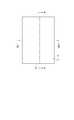
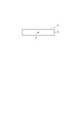
このような多光子吸収を利用する本実施形態に係るレーザ加工方法の原理について、図1〜図6を参照して説明する。図1に示すように、板状の加工対象物1の表面3には、加工対象物1を切断するための切断予定ライン5がある。切断予定ライン5は直線状に延びた仮想線である。本実施形態に係るレーザ加工方法では、図2に示すように、多光子吸収が生じる条件で加工対象物1の内部に集光点Pを合わせてレーザ光Lを照射して改質領域7を形成する。なお、集光点Pとは、レーザ光Lが集光する箇所のことである。また、切断予定ライン5は、直線状に限らず曲線状であってもよいし、仮想線に限らず加工対象物1に実際に引かれた線であってもよい。 The principle of the laser processing method according to this embodiment using such multiphoton absorption will be described with reference to FIGS. As shown in FIG. 1, there is a scheduled
そして、レーザ光Lを切断予定ライン5に沿って(すなわち、図1の矢印A方向に)相対的に移動させることにより、集光点Pを切断予定ライン5に沿って移動させる。これにより、図3〜図5に示すように、改質領域7が切断予定ライン5に沿って加工対象物1の内部に形成され、この改質領域7が切断起点領域8となる。ここで、切断起点領域8とは、加工対象物1が切断される際に切断(割れ)の起点となる領域を意味する。この切断起点領域8は、改質領域7が連続的に形成されることで形成される場合もあるし、改質領域7が断続的に形成されることで形成される場合もある。 Then, the condensing point P is moved along the
本実施形態に係るレーザ加工方法は、加工対象物1がレーザ光Lを吸収することにより加工対象物1を発熱させて改質領域7を形成するものではない。加工対象物1にレーザ光Lを透過させ加工対象物1の内部に多光子吸収を発生させて改質領域7を形成している。よって、加工対象物1の表面3ではレーザ光Lがほとんど吸収されないので、加工対象物1の表面3が溶融することはない。 The laser processing method according to the present embodiment does not form the modified
加工対象物1の内部に切断起点領域8を形成すると、この切断起点領域8を起点として割れが発生し易くなるため、図6に示すように、比較的小さな力で加工対象物1を切断することができる。よって、加工対象物1の表面3に不必要な割れを発生させることなく、加工対象物1を高精度に切断することが可能になる。 If the cutting
この切断起点領域8を起点とした加工対象物1の切断には、次の2通りが考えられる。1つは、切断起点領域8形成後、加工対象物1に人為的な力が印加されることにより、切断起点領域8を起点として加工対象物1が割れ、加工対象物1が切断される場合である。これは、例えば加工対象物1の厚さが大きい場合の切断である。人為的な力が印加されるとは、例えば、加工対象物1の切断起点領域8に沿って加工対象物1に曲げ応力やせん断応力を加えたり、加工対象物1に温度差を与えることにより熱応力を発生させたりすることである。他の1つは、切断起点領域8を形成することにより、切断起点領域8を起点として加工対象物1の断面方向(厚さ方向)に向かって自然に割れ、結果的に加工対象物1が切断される場合である。これは、例えば加工対象物1の厚さが小さい場合には、1列の改質領域7により切断起点領域8が形成されることで可能となり、加工対象物1の厚さが大きい場合には、厚さ方向に複数列形成された改質領域7により切断起点領域8が形成されることで可能となる。なお、この自然に割れる場合も、切断する箇所において、切断起点領域8が形成されていない部位に対応する部分の表面3上にまで割れが先走ることがなく、切断起点領域8を形成した部位に対応する部分のみを割断することができるので、割断を制御よくすることができる。近年、シリコンウェハ等の加工対象物1の厚さは薄くなる傾向にあるので、このような制御性のよい割断方法は大変有効である。 The following two types of cutting of the
さて、本実施形態に係るレーザ加工方法において、多光子吸収により形成される改質領域としては、次の(1)〜(4)の場合がある。 In the laser processing method according to the present embodiment, the modified regions formed by multiphoton absorption include the following cases (1) to (4).
(1)改質領域が1つ又は複数のクラックを含むクラック領域の場合
加工対象物(例えばガラスやLiTaO3からなる圧電材料)の内部に集光点を合わせて、集光点における電界強度が1×10⁸(W/cm2)以上で且つパルス幅が1μs以下の条件でレーザ光を照射する。このパルス幅の大きさは、多光子吸収を生じさせつつ加工対象物の表面に余計なダメージを与えずに、加工対象物の内部にのみクラック領域を形成できる条件である。これにより、加工対象物の内部には多光子吸収による光学的損傷という現象が発生する。この光学的損傷により加工対象物の内部に熱ひずみが誘起され、これにより加工対象物の内部にクラック領域が形成される。電界強度の上限値としては、例えば1×1012(W/cm2)である。パルス幅は例えば1ns〜200nsが好ましい。なお、多光子吸収によるクラック領域の形成は、例えば、第45回レーザ熱加工研究会論文集(1998年.12月)の第23頁〜第28頁の「固体レーザー高調波によるガラス基板の内部マーキング」に記載されている。(1) In the case where the modified region is a crack region including one or a plurality of cracks, the focusing point is set inside the object to be processed (for example, a piezoelectric material made of glass or LiTaO3 ), and the electric field strength at the focusing point is Irradiation with laser light is performed under conditions of 1 × 10⁸ (W / cm2 ) or more and a pulse width of 1 μs or less. The magnitude of this pulse width is a condition that allows a crack region to be formed only inside the workpiece without causing extra damage to the surface of the workpiece while causing multiphoton absorption. As a result, a phenomenon of optical damage due to multiphoton absorption occurs inside the workpiece. This optical damage induces thermal strain inside the workpiece, thereby forming a crack region inside the workpiece. The upper limit value of the electric field strength is, for example, 1 × 10¹² (W / cm2 ). The pulse width is preferably 1 ns to 200 ns, for example. The formation of the crack region by multiphoton absorption is described in, for example, “Inside of glass substrate by solid-state laser harmonics” on pages 23-28 of the 45th Laser Thermal Processing Research Papers (December 1998) It is described in “Marking”.
本発明者は、電界強度とクラックの大きさとの関係を実験により求めた。実験条件は次ぎの通りである。 The inventor obtained the relationship between the electric field strength and the size of the cracks by experiment. The experimental conditions are as follows.
(A)加工対象物:パイレックス(登録商標)ガラス(厚さ700μm)
(B)レーザ
光源:半導体レーザ励起Nd:YAGレーザ
波長:1064nm
レーザ光スポット断面積:3.14×10⁻⁸cm2
発振形態:Qスイッチパルス
繰り返し周波数:100kHz
パルス幅:30ns
出力:出力<1mJ/パルス
レーザ光品質:TEM00
偏光特性:直線偏光
(C)集光用レンズ
レーザ光波長に対する透過率:60パーセント
(D)加工対象物が載置される載置台の移動速度:100mm/秒(A) Workpiece: Pyrex (registered trademark) glass (thickness 700 μm)
(B) Laser
Light source: Semiconductor laser pumped Nd: YAG laser
Wavelength: 1064nm
Laser light spot cross-sectional area: 3.14 × 10⁻⁸ cm2
Oscillation form: Q switch pulse
Repeat frequency: 100 kHz
Pulse width: 30ns
Output: Output <1mJ / pulse
Laser light quality: TEM00
Polarization characteristics: Linearly polarized light (C) Condensing lens
Transmittance with respect to laser beam wavelength: 60% (D) Moving speed of mounting table on which workpiece is mounted: 100 mm / second
なお、レーザ光品質がTEM00とは、集光性が高くレーザ光の波長程度まで集光可能を意味する。Note that the laser light quality TEM00 means that the light condensing performance is high and the light can be condensed up to the wavelength of the laser light.
図7は上記実験の結果を示すグラフである。横軸はピークパワー密度であり、レーザ光がパルスレーザ光なので電界強度はピークパワー密度で表される。縦軸は1パルスのレーザ光により加工対象物の内部に形成されたクラック部分(クラックスポット)の大きさを示している。クラックスポットが集まりクラック領域となる。クラックスポットの大きさは、クラックスポットの形状のうち最大の長さとなる部分の大きさである。グラフ中の黒丸で示すデータは集光用レンズ(C)の倍率が100倍、開口数(NA)が0.80の場合である。一方、グラフ中の白丸で示すデータは集光用レンズ(C)の倍率が50倍、開口数(NA)が0.55の場合である。ピークパワー密度が1011(W/cm2)程度から加工対象物の内部にクラックスポットが発生し、ピークパワー密度が大きくなるに従いクラックスポットも大きくなることが分かる。FIG. 7 is a graph showing the results of the experiment. The horizontal axis represents the peak power density. Since the laser beam is a pulsed laser beam, the electric field strength is represented by the peak power density. The vertical axis represents the size of a crack portion (crack spot) formed inside the workpiece by one pulse of laser light. Crack spots gather to form a crack region. The size of the crack spot is the size of the portion having the maximum length in the shape of the crack spot. Data indicated by black circles in the graph is for the case where the magnification of the condenser lens (C) is 100 times and the numerical aperture (NA) is 0.80. On the other hand, the data indicated by the white circles in the graph is when the magnification of the condenser lens (C) is 50 times and the numerical aperture (NA) is 0.55. From the peak power density of about 1011 (W / cm2 ), it can be seen that a crack spot is generated inside the workpiece, and the crack spot increases as the peak power density increases.
次に、クラック領域形成による加工対象物の切断のメカニズムについて、図8〜図11を参照して説明する。図8に示すように、多光子吸収が生じる条件で加工対象物1の内部に集光点Pを合わせてレーザ光Lを照射して切断予定ラインに沿って内部にクラック領域9を形成する。クラック領域9は1つ又は複数のクラックを含む領域である。このように形成されたクラック領域9が切断起点領域となる。図9に示すように、クラック領域9を起点として(すなわち、切断起点領域を起点として)クラックがさらに成長し、図10に示すように、クラックが加工対象物1の表面3と裏面21とに到達し、図11に示すように、加工対象物1が割れることにより加工対象物1が切断される。加工対象物1の表面3と裏面21とに到達するクラックは自然に成長する場合もあるし、加工対象物1に力が印加されることにより成長する場合もある。 Next, the mechanism of cutting the workpiece by forming the crack region will be described with reference to FIGS. As shown in FIG. 8, under the condition that multiphoton absorption occurs, the converging point P is aligned with the inside of the
(2)改質領域が溶融処理領域の場合
加工対象物(例えばシリコンのような半導体材料)の内部に集光点を合わせて、集光点における電界強度が1×10⁸(W/cm2)以上で且つパルス幅が1μs以下の条件でレーザ光を照射する。これにより加工対象物の内部は多光子吸収によって局所的に加熱される。この加熱により加工対象物の内部に溶融処理領域が形成される。溶融処理領域とは一旦溶融後再固化した領域や、まさに溶融状態の領域や、溶融状態から再固化する状態の領域であり、相変化した領域や結晶構造が変化した領域ということもできる。また、溶融処理領域とは単結晶構造、非晶質構造、多結晶構造において、ある構造が別の構造に変化した領域ということもできる。つまり、例えば、単結晶構造から非晶質構造に変化した領域、単結晶構造から多結晶構造に変化した領域、単結晶構造から非晶質構造及び多結晶構造を含む構造に変化した領域を意味する。加工対象物がシリコン単結晶構造の場合、溶融処理領域は例えば非晶質シリコン構造である。電界強度の上限値としては、例えば1×1012(W/cm2)である。パルス幅は例えば1ns〜200nsが好ましい。(2) When the reforming region is a melt processing region The focusing point is set inside the object to be processed (for example, a semiconductor material such as silicon), and the electric field strength at the focusing point is 1 × 10⁸ (W / cm2). ) Irradiation with laser light is performed under the above conditions with a pulse width of 1 μs or less. As a result, the inside of the workpiece is locally heated by multiphoton absorption. By this heating, a melt processing region is formed inside the workpiece. The melt treatment region is a region once solidified after melting, a region in a molten state, or a region re-solidified from a molten state, and can also be referred to as a phase-changed region or a region in which the crystal structure has changed. The melt treatment region can also be said to be a region in which one structure is changed to another structure in a single crystal structure, an amorphous structure, or a polycrystalline structure. In other words, for example, a region changed from a single crystal structure to an amorphous structure, a region changed from a single crystal structure to a polycrystalline structure, or a region changed from a single crystal structure to a structure including an amorphous structure and a polycrystalline structure. To do. When the object to be processed has a silicon single crystal structure, the melt processing region has, for example, an amorphous silicon structure. The upper limit value of the electric field strength is, for example, 1 × 10¹² (W / cm2 ). The pulse width is preferably 1 ns to 200 ns, for example.
本発明者は、シリコンウェハの内部で溶融処理領域が形成されることを実験により確認した。実験条件は次の通りである。 The inventor has confirmed through experiments that a melt-processed region is formed inside a silicon wafer. The experimental conditions are as follows.
(A)加工対象物:シリコンウェハ(厚さ350μm、外径4インチ)
(B)レーザ
光源:半導体レーザ励起Nd:YAGレーザ
波長:1064nm
レーザ光スポット断面積:3.14×10⁻⁸cm2
発振形態:Qスイッチパルス
繰り返し周波数:100kHz
パルス幅:30ns
出力:20μJ/パルス
レーザ光品質:TEM00
偏光特性:直線偏光
(C)集光用レンズ
倍率:50倍
N.A.:0.55
レーザ光波長に対する透過率:60パーセント
(D)加工対象物が載置される載置台の移動速度:100mm/秒(A) Workpiece: silicon wafer (thickness 350 μm,
(B) Laser
Light source: Semiconductor laser pumped Nd: YAG laser
Wavelength: 1064nm
Laser light spot cross-sectional area: 3.14 × 10⁻⁸ cm2
Oscillation form: Q switch pulse
Repeat frequency: 100 kHz
Pulse width: 30ns
Output: 20μJ / pulse
Laser light quality: TEM00
Polarization characteristics: Linearly polarized light (C) Condensing lens
Magnification: 50 times
N. A. : 0.55
Transmittance with respect to laser beam wavelength: 60% (D) Moving speed of mounting table on which workpiece is mounted: 100 mm / second
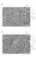
図12は、上記条件でのレーザ加工により切断されたシリコンウェハの一部における断面の写真を表した図である。シリコンウェハ11の内部に溶融処理領域13が形成されている。なお、上記条件により形成された溶融処理領域13の厚さ方向の大きさは100μm程度である。 FIG. 12 is a view showing a photograph of a cross section of a part of a silicon wafer cut by laser processing under the above conditions. A
溶融処理領域13が多光子吸収により形成されたことを説明する。図13は、レーザ光の波長とシリコン基板の内部の透過率との関係を示すグラフである。ただし、シリコン基板の表面側と裏面側それぞれの反射成分を除去し、内部のみの透過率を示している。シリコン基板の厚さtが50μm、100μm、200μm、500μm、1000μmの各々について上記関係を示した。 The fact that the
例えば、Nd:YAGレーザの波長である1064nmにおいて、シリコン基板の厚さが500μm以下の場合、シリコン基板の内部ではレーザ光が80%以上透過することが分かる。図12に示すシリコンウェハ11の厚さは350μmであるので、多光子吸収による溶融処理領域13はシリコンウェハ11の中心付近、つまり表面から175μmの部分に形成される。この場合の透過率は、厚さ200μmのシリコンウェハを参考にすると、90%以上なので、レーザ光がシリコンウェハ11の内部で吸収されるのは僅かであり、ほとんどが透過する。このことは、シリコンウェハ11の内部でレーザ光が吸収されて、溶融処理領域13がシリコンウェハ11の内部に形成(つまりレーザ光による通常の加熱で溶融処理領域が形成)されたものではなく、溶融処理領域13が多光子吸収により形成されたことを意味する。多光子吸収による溶融処理領域の形成は、例えば、溶接学会全国大会講演概要第66集(2000年4月)の第72頁〜第73頁の「ピコ秒パルスレーザによるシリコンの加工特性評価」に記載されている。 For example, when the thickness of the silicon substrate is 500 μm or less at the wavelength of the Nd: YAG laser of 1064 nm, it can be seen that the laser light is transmitted by 80% or more inside the silicon substrate. Since the thickness of the
なお、シリコンウェハは、溶融処理領域によって形成される切断起点領域を起点として断面方向に向かって割れを発生させ、その割れがシリコンウェハの表面と裏面とに到達することにより、結果的に切断される。シリコンウェハの表面と裏面に到達するこの割れは自然に成長する場合もあるし、シリコンウェハに力が印加されることにより成長する場合もある。そして、切断起点領域からシリコンウェハの表面と裏面とに割れが自然に成長する場合には、切断起点領域を形成する溶融処理領域が溶融している状態から割れが成長する場合と、切断起点領域を形成する溶融処理領域が溶融している状態から再固化する際に割れが成長する場合とのいずれもある。ただし、どちらの場合も溶融処理領域はシリコンウェハの内部のみに形成され、切断後の切断面には、図12のように内部にのみ溶融処理領域が形成されている。このように、加工対象物の内部に溶融処理領域によって切断起点領域を形成すると、割断時、切断起点領域ラインから外れた不必要な割れが生じにくいので、割断制御が容易となる。 Note that a silicon wafer is cracked as a result of generating cracks in the cross-sectional direction starting from the cutting start region formed by the melt processing region and reaching the front and back surfaces of the silicon wafer. The The cracks that reach the front and back surfaces of the silicon wafer may grow naturally or may grow by applying force to the silicon wafer. And when a crack naturally grows from the cutting start region to the front and back surfaces of the silicon wafer, the case where the crack grows from a state where the melt treatment region forming the cutting starting region is melted, and the cutting starting region There are both cases where cracks grow when the solidified region is melted from the molten state. However, in either case, the melt processing region is formed only inside the silicon wafer, and the melt processing region is formed only inside the cut surface after cutting as shown in FIG. In this way, when the cutting start region is formed by the melt processing region inside the workpiece, unnecessary cracking off the cutting start region line is unlikely to occur during cleaving, so that cleaving control is facilitated.
(3)改質領域が溶融処理領域及び微小空洞の場合
加工対象物(例えばシリコンのような半導体材料)の内部に集光点を合わせて、集光点における電界強度が1×10⁸(W/cm2)以上で且つパルス幅が1μs以下の条件でレーザ光を照射する。これにより、加工対象物の内部には溶融処理領域と微小空洞とが形成される場合がある。なお、電界強度の上限値としては、例えば1×1012(W/cm2)である。パルス幅は例えば1ns〜200nsが好ましい。(3) When the modified region is a melt-processed region and a microcavity The focusing point is set inside the object to be processed (for example, a semiconductor material such as silicon), and the electric field strength at the focusing point is 1 × 10⁸ (W / Cm2 ) or more and the pulse width is 1 μs or less. As a result, a melt processing region and a microcavity may be formed inside the workpiece. In addition, as an upper limit of an electric field strength, it is 1 * 10 <12 > (W / cm <2 >), for example. The pulse width is preferably 1 ns to 200 ns, for example.
図14に示すように、シリコンウェハ11の表面3側からレーザ光Lを入射させた場合、微小空洞14は、溶融処理領域13に対して裏面21側に形成される。図14では、溶融処理領域13と微小空洞14とが離れて形成されているが、溶融処理領域13と微小空洞14とが連続して形成される場合もある。つまり、多光子吸収によって溶融処理領域13及び微小空洞14が対になって形成される場合、微小空洞14は、溶融処理領域13に対してシリコンウェハ11におけるレーザ光入射面の反対側に形成されることになる。 As shown in FIG. 14, when the laser beam L is incident from the
このように、シリコンウェハ11にレーザ光Lを透過させシリコンウェハ11の内部に多光子吸収を発生させて溶融処理領域13を形成した場合に、それぞれの溶融処理領域13に対応した微小空洞14が形成される原理については必ずしも明らかではない。ここでは、溶融処理領域13及び微小空洞14が対になった状態で形成される原理に関して本発明者らが想定する2つの仮説を説明する。 As described above, when the
本発明者らが想定する第1の仮説は次の通りである。すなわち、図15に示すように、シリコンウェハ11の内部の集光点Pに焦点を合わせてレーザ光Lを照射すると、集光点Pの近傍に溶融処理領域13が形成される。従来は、このレーザ光Lとして、レーザ光源から照射されるレーザ光Lの中心部分の光(図15中、L4及びL5に相当する部分の光)を使用することとしていた。これは、レーザ光Lのガウシアン分布の中心部分を使用するためである。 The first hypothesis assumed by the present inventors is as follows. That is, as shown in FIG. 15, when the laser beam L is focused on the condensing point P inside the
本発明者らはレーザ光Lがシリコンウェハ11の表面3に与える影響をおさえるためにレーザ光Lを広げることとした。その一手法として、レーザ光源から照射されるレーザ光Lを所定の光学系でエキスパンドしてガウシアン分布の裾野を広げて、レーザ光Lの周辺部分の光(図15中、L1〜L3及びL6〜L8に相当する部分の光)のレーザ強度を相対的に上昇させることとした。このようにエキスパンドしたレーザ光Lをシリコンウェハ11に透過させると、既に説明したように集光点Pの近傍では溶融処理領域13が形成され、その溶融処理領域13に対応した部分に微小空洞14が形成される。つまり、溶融処理領域13と微小空洞14とはレーザ光Lの光軸(図15中の一点鎖線)に沿った位置に形成される。微小空洞14が形成される位置は、レーザ光Lの周辺部分の光(図15中、L1〜L3及びL6〜L8に相当する部分の光)が理論上集光される部分に相当する。 The inventors decided to broaden the laser light L in order to suppress the influence of the laser light L on the
このようにレーザ光Lの中心部分の光(図15中、L4及びL5に相当する部分の光)と、レーザ光Lの周辺部分の光(図15中、L1〜L3及びL6〜L8に相当する部分の光)とがそれぞれ集光される部分がシリコンウェハ11の厚さ方向において異なるのは、レーザ光Lを集光するレンズの球面収差によるものと考えられる。本発明者らが想定する第1の仮説は、この集光位置の差が何らかの影響を及ぼしているのではないかというものである。 As described above, light at the center of the laser light L (light corresponding to L4 and L5 in FIG. 15) and light at the peripheral portion of the laser light L (corresponding to L1 to L3 and L6 to L8 in FIG. 15). It is considered that the portions where the light is condensed in the thickness direction of the
本発明者らが想定する第2の仮説は、レーザ光Lの周辺部分の光(図15中、L1〜L3及びL6〜L8に相当する部分の光)が集光される部分は理論上のレーザ集光点であるから、この部分の光強度が高く微細構造変化が起こっているためにその周囲が実質的に結晶構造が変化していない微小空洞14が形成され、溶融処理領域13が形成されている部分は熱的な影響が大きく単純に溶解して再固化したというものである。 The second hypothesis assumed by the present inventors is that the portion where the light around the laser beam L (the portions corresponding to L1 to L3 and L6 to L8 in FIG. 15) is condensed is theoretically Since it is a laser condensing point, since the light intensity of this portion is high and a fine structure change has occurred, a
ここで、溶融処理領域13は上記(2)で述べた通りのものであるが、微小空洞14は、その周囲が実質的に結晶構造が変化していないものである。シリコンウェハ11がシリコン単結晶構造の場合には、微小空洞14の周囲はシリコン単結晶構造のままの部分が多い。 Here, the melt-processed
本発明者らは、シリコンウェハ11の内部で溶融処理領域13及び微小空洞14が形成されることを実験により確認した。実験条件は次の通りである。 The present inventors have confirmed through experiments that the
(A)加工対象物:シリコンウェハ(厚さ100μm)
(B)レーザ
光源:半導体レーザ励起Nd:YAGレーザ
波長:1064nm
繰り返し周波数:40kHz
パルス幅:30ns
パルスピッチ:7μm
加工深さ:8μm
パルスエネルギー:50μJ/パルス
(C)集光用レンズ
NA:0.55
(D)加工対象物が載置される載置台の移動速度:280mm/秒(A) Workpiece: silicon wafer (
(B) Laser Light source: Semiconductor laser excitation Nd: YAG laser Wavelength: 1064 nm
Repeat frequency: 40 kHz
Pulse width: 30ns
Pulse pitch: 7μm
Processing depth: 8μm
Pulse energy: 50 μJ / pulse (C) Condensing lens NA: 0.55
(D) Movement speed of the mounting table on which the workpiece is placed: 280 mm / second
図16は、上記条件でのレーザ加工により切断されたシリコンウェハ11の切断面の写真を表した図である。図16において(a)と(b)とは同一の切断面の写真を異なる縮尺で示したものである。同図に示すように、シリコンウェハ11の内部には、1パルスのレーザ光Lの照射により形成された溶融処理領域13及び微小空洞14の対が、切断面に沿って(すなわち、切断予定ラインに沿って)所定のピッチで形成されている。 FIG. 16 is a view showing a photograph of a cut surface of the
なお、図16に示す切断面の溶融処理領域13は、シリコンウェハ11の厚さ方向(図中の上下方向)の幅が13μm程度で、レーザ光Lを移動する方向(図中の左右方向)の幅が3μm程度である。また、微小空洞14は、シリコンウェハ11の厚さ方向の幅が7μm程度で、レーザ光Lを移動する方向の幅が1.3μm程度である。溶融処理領域13と微小空洞14との間隔は1.2μm程度である。 16 has a width of about 13 μm in the thickness direction (vertical direction in the figure) of the
(4)改質領域が屈折率変化領域の場合
加工対象物(例えばガラス)の内部に集光点を合わせて、集光点における電界強度が1×10⁸(W/cm2)以上で且つパルス幅が1ns以下の条件でレーザ光を照射する。パルス幅を極めて短くして、多光子吸収を加工対象物の内部に起こさせると、多光子吸収によるエネルギーが熱エネルギーに転化せずに、加工対象物の内部にはイオン価数変化、結晶化又は分極配向等の永続的な構造変化が誘起されて屈折率変化領域が形成される。電界強度の上限値としては、例えば1×1012(W/cm2)である。パルス幅は例えば1ns以下が好ましく、1ps以下がさらに好ましい。多光子吸収による屈折率変化領域の形成は、例えば、第42回レーザ熱加工研究会論文集(1997年.11月)の第105頁〜第111頁の「フェムト秒レーザー照射によるガラス内部への光誘起構造形成」に記載されている。(4) When the modified region is a refractive index changing region The focusing point is set inside the object to be processed (for example, glass), and the electric field strength at the focusing point is 1 × 10⁸ (W / cm2 ) or more and Laser light is irradiated under the condition that the pulse width is 1 ns or less. When the pulse width is made extremely short and multiphoton absorption occurs inside the workpiece, the energy due to the multiphoton absorption is not converted into thermal energy, and the ion valence change and crystallization occur inside the workpiece. Alternatively, a permanent structural change such as polarization orientation is induced to form a refractive index change region. The upper limit value of the electric field strength is, for example, 1 × 10¹² (W / cm2 ). For example, the pulse width is preferably 1 ns or less, and more preferably 1 ps or less. The formation of the refractive index changing region by multiphoton absorption is described in, for example, “The Femtosecond Laser Irradiation to the Inside of Glass” on pages 105 to 111 of the 42nd Laser Thermal Processing Research Institute Proceedings (November 1997). Photo-induced structure formation ”.
以上、多光子吸収により形成される改質領域として(1)〜(4)の場合を説明したが、ウェハ状の加工対象物の結晶構造やその劈開性などを考慮して切断起点領域を次のように形成すれば、その切断起点領域を起点として、より一層小さな力で、しかも精度良く加工対象物を切断することが可能になる。 As described above, the cases of (1) to (4) have been described as the modified regions formed by multiphoton absorption. However, the cutting starting region is determined in consideration of the crystal structure of the wafer-like workpiece and its cleavage. If it forms in this way, it will become possible to cut | disconnect a process target object with much smaller force from the cutting | disconnection starting point area | region as a starting point, and still more accurately.
すなわち、シリコンなどのダイヤモンド構造の単結晶半導体からなる基板の場合は、(111)面(第1劈開面)や(110)面(第2劈開面)に沿った方向に切断起点領域を形成するのが好ましい。また、GaAsなどの閃亜鉛鉱型構造のIII−V族化合物半導体からなる基板の場合は、(110)面に沿った方向に切断起点領域を形成するのが好ましい。さらに、サファイア(Al2O3)などの六方晶系の結晶構造を有する基板の場合は、(0001)面(C面)を主面として(1120)面(A面)或いは(1100)面(M面)に沿った方向に切断起点領域を形成するのが好ましい。That is, in the case of a substrate made of a single crystal semiconductor having a diamond structure such as silicon, the cutting start region is formed in a direction along the (111) plane (first cleavage plane) or the (110) plane (second cleavage plane). Is preferred. In the case of a substrate made of a zinc-blende-type III-V group compound semiconductor such as GaAs, it is preferable to form the cutting start region in the direction along the (110) plane. Further, in the case of a substrate having a hexagonal crystal structure such as sapphire (Al2 O3 ), the (1120) plane (A plane) or (1100) plane ( It is preferable to form the cutting start region in a direction along the (M plane).
なお、上述した切断起点領域を形成すべき方向(例えば、単結晶シリコン基板における(111)面に沿った方向)、或いは切断起点領域を形成すべき方向に直交する方向に沿って基板にオリエンテーションフラットを形成すれば、そのオリエンテーションフラットを基準とすることで、切断起点領域を形成すべき方向に沿った切断起点領域を容易且つ正確に基板に形成することが可能になる。
[第1実施形態]Note that the orientation flat on the substrate along the direction in which the above-described cutting start region is to be formed (for example, the direction along the (111) plane in the single crystal silicon substrate) or the direction perpendicular to the direction in which the cutting start region is to be formed By using the orientation flat as a reference, it is possible to easily and accurately form the cutting start area along the direction in which the cutting start area is to be formed on the substrate.
[First Embodiment]
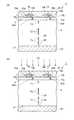
次に、本発明の第1実施形態について説明する。図17は、本実施形態のレーザ加工方法における加工対象物の平面図であり、図18は、図17に示す加工対象物のXVIII−XVIII線に沿っての部分断面図である。 Next, a first embodiment of the present invention will be described. FIG. 17 is a plan view of an object to be processed in the laser processing method of the present embodiment, and FIG. 18 is a partial cross-sectional view along the line XVIII-XVIII of the object to be processed shown in FIG.
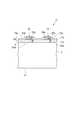
図17及び図18に示すように、加工対象物1は、シリコンからなる厚さ300μm、外径6インチの基板4と、複数の機能素子15を含んで基板4の表面3に形成された積層部16とを備えている。機能素子15は、基板4の表面3に積層された層間絶縁膜17aと、層間絶縁膜17a上に配置された配線層19aと、配線層19aを覆うように層間絶縁膜17a上に積層された層間絶縁膜17bと、層間絶縁膜17b上に配置された配線層19bとを有している。配線層19aと基板4とは、層間絶縁膜17aを貫通する導電性プラグ20aによって電気的に接続され、配線層19bと配線層19aとは、層間絶縁膜17bを貫通する導電性プラグ20bによって電気的に接続されている。 As shown in FIGS. 17 and 18, the
なお、機能素子15は、基板4のオリエンテーションフラット6に平行な方向及び垂直な方向にマトリックス状に多数形成されているが、層間絶縁膜17a,17bは、基板4の表面3全体を覆うように隣り合う機能素子15,15間に渡って形成されている。 A large number of
以上のように構成された加工対象物1を以下のようにして機能素子15毎に切断する(ここでは、平面視5mm×5mmの正方形薄板状のチップに切断する)。まず、図19(a)に示すように、積層部16を覆うように加工対象物1に保護テープ22を貼り付ける。続いて、図19(b)に示すように、基板4の裏面21を上方に向けて加工対象物1をレーザ加工装置の載置台(図示せず)上に固定する。このとき、積層部16が載置台に直接接触することが保護テープ22によって避けられるため、各機能素子15を保護することができる。 The
そして、隣り合う機能素子15,15間を通るように切断予定ライン5を5mm間隔で格子状に設定し(図17の破線参照)、裏面21をレーザ光入射面として基板4の内部に集光点Pを合わせてレーザ光Lを多光子吸収が生じる条件で照射する。同時に、載置台の移動により、切断予定ライン5に沿ってレーザ光Lを加工対象物1に対して相対移動させる。 Then, the
この切断予定ライン5に沿ってのレーザ光Lの相対移動を1本の切断予定ライン5に対して6回行うが、集光点Pを合わせる位置の裏面21からの距離を毎回変えることで、表面3側から順に、1列の品質改質領域(第2の改質領域)71、3列の分断改質領域(第1の改質領域)72、及び2列のHC(ハーフカット)改質領域(第3の改質領域)73を切断予定ライン5に沿って基板4の内部に1列ずつ形成する。なお、基板4はシリコンからなる半導体基板であるため、各改質領域71,72,73は溶融処理領域であるが、クラックを含む場合もある。 The relative movement of the laser light L along the
ここで、品質改質領域71の形成及びHC改質領域73の形成においては、切断予定ライン5に沿ってレーザ光Lを加工対象物1に対して相対移動させる速度(以下、単に「レーザ光Lの移動速度」という)を300mm/秒とした。これに対し、分断改質領域72の形成においては、レーザ光Lの移動速度を600mm/秒とした。なお、レーザ光Lの光源の繰り返し周波数については、80kHzで一定とした。 Here, in the formation of the
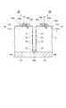
これにより、図22に示すように、1パルスのレーザ光Lの照射により形成される分断改質領域72の形成間隔は、1パルスのレーザ光Lの照射により形成される品質改質領域71の形成間隔及びHC改質領域73の形成間隔より大きくなった。すなわち、分断改質領域72の形成密度は、品質改質領域71の形成密度及びHC改質領域73の形成密度より低くなった。 As a result, as shown in FIG. 22, the formation interval of the divided modified
なお、品質改質領域71の形成においては、基板4の表面3と品質改質領域71の表面側端部71aとの距離が5μm〜20μmとなるように品質改質領域71を1列形成した。また、分断改質領域72の形成においては、基板4の厚さ方向において一続きとなるように分断改質領域72を3列形成した。更に、HC改質領域73の形成においては、図19(b)に示すように、HC改質領域73を2列形成することで、切断予定ライン5に沿った割れ24をHC改質領域73から基板4の裏面21に生じさせた(形成条件によっては、隣り合う分断改質領域72とHC改質領域73との間にも割れ24が生じる場合がある)。 In the formation of the quality modified
各改質領域71,72,73を形成した後、図20(a)に示すように、加工対象物1の基板4の裏面21にエキスパンドテープ23を貼り付ける。続いて、図20(b)に示すように、保護テープ22に紫外線を照射して、その粘着力を低下させ、図21(a)に示すように、加工対象物1の積層部16から保護テープ22を剥がす。 After forming the respective modified
保護テープ22を剥がした後、図21(b)に示すように、エキスパンドテープ23を拡張させて、各改質領域71,72,73を起点として割れを生じさせ、加工対象物1を切断予定ライン5に沿って機能素子15毎に切断すると共に、切断されて得られた各半導体チップ25を互いに離間させる。 After peeling off the
以上説明したように、上記レーザ加工方法では、分断改質領域72を形成する際のレーザ光Lの移動速度(600mm/秒)を、品質改質領域71及びHC改質領域73を形成する際のレーザ光Lの移動速度(300mm/秒)より速くしている。そして、分断改質領域72の形成密度を品質改質領域71の形成密度及びHC改質領域73の形成密度より低くしている。そのため、分断改質領域72の形成密度を品質改質領域71の形成密度及びHC改質領域73の形成密度と同等にする場合に比べ、1本の切断予定ライン5に対して全ての改質領域71,72,73を形成する時間を短くすることできる。 As described above, in the laser processing method, the moving speed (600 mm / second) of the laser beam L when forming the divided modified
具体的には、レーザ光Lの移動速度を300mm/秒として1本の切断予定ライン5に対して全ての改質領域71,72,73を形成するのには約1.0秒を要したが、上記レーザ加工方法によれば約0.5秒で済んだ。また、レーザ光Lの移動速度を300mm/秒として基板4の内部に全ての改質領域71,72,73を形成するのには約342秒を要したが、上記レーザ加工方法によれば約256.5秒で済んだ。 Specifically, it took about 1.0 second to form all the modified
ところで、品質改質領域71及びHC改質領域73は、分断改質領域72に比べ、加工対象物1の切断品質に大きな影響を与える。例えば、品質改質領域71の表面側端部71aと基板4の表面3との距離が5μm〜20μmとなるように品質改質領域71が形成されていると、基板4の表面3に形成された積層部16を基板4と共に切断予定ライン5に沿って精度良く切断することが可能になる。また、切断予定ライン5に沿った割れ24がHC改質領域73から基板4の裏面21に生じるようにHC改質領域73が形成されていると、エキスパンドテープ23を拡張させた際に割れ24が分断改質領域72及び品質改質領域71を介して基板4の表面3に向かってスムーズに進行することになり、その結果、加工対象物1を切断予定ライン5に沿って精度良く切断することが可能になる。 By the way, the
上記レーザ加工方法では、加工対象物1の切断品質に大きな影響を与える品質改質領域71及びHC改質領域73の形成密度を分断改質領域72の形成密度より高くしているため、加工対象物1の切断品質の劣化を防止することができる。 In the laser processing method, since the formation density of the quality modified
また、上記レーザ加工方法では、各改質領域71,72,73を基板4の裏面21から遠い順に一列ずつ形成するので、各改質領域71,72,73を形成するに際し、レーザ光入射面である裏面21とレーザ光Lの集光点Pとの間には改質領域が存在しない。そのため、既に形成された改質領域によるレーザ光Lの散乱、吸収等が起こることはない。従って、各改質領域71,72,73を切断予定ライン5に沿って基板4の内部に精度良く形成することができる。 In the laser processing method, the modified
更に、上記レーザ加工方法では、基板4の裏面21をレーザ光入射面とするため、積層部16の切断予定ライン5上にレーザ光Lを反射する部材(例えば、TEG)が存在しても、各改質領域71,72,73を切断予定ライン5に沿って基板4の内部に確実に形成することができる。 Further, in the above laser processing method, since the
そして、以上のようなレーザ加工方法の使用により切断された半導体チップ25においては、図21(b)に示すように、各改質領域71,72,73が形成された基板4の切断面(側面)4a、及び積層部16の切断面16aは、凹凸が抑制された高精度な切断面となる。
[第2実施形態]And in the
[Second Embodiment]
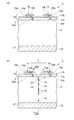
次に、本発明の第2実施形態について説明する。第2実施形態のレーザ加工方法は、基板4の表面3をレーザ光入射面とする点で、基板4の裏面21をレーザ光入射面とする第1実施形態のレーザ加工方法と異なっている。 Next, a second embodiment of the present invention will be described. The laser processing method of the second embodiment is different from the laser processing method of the first embodiment in that the
すなわち、図23(a)に示すように、基板4の裏面21にエキスパンドテープ23を貼り付ける。続いて、図23(b)に示すように、積層部16を上方に向けて加工対象物1をレーザ加工装置の載置台(図示せず)上に固定する。 That is, as shown in FIG. 23A, the expanded
そして、隣り合う機能素子15,15間を通るように切断予定ライン5を格子状に設定し(図17の破線参照)、表面3をレーザ光入射面として基板4の内部に集光点Pを合わせて積層部16側からレーザ光Lを多光子吸収が生じる条件で照射する。同時に、載置台の移動により、切断予定ライン5に沿ってレーザ光Lを加工対象物1に対して相対移動させる。 Then, the
この切断予定ライン5に沿ってのレーザ光Lの相対移動を1本の切断予定ライン5に対して6回行うが、集光点Pを合わせる位置の表面3からの距離を毎回変えることで、裏面21側から順に、4列の分断改質領域(第3の改質領域)72、1列の補助HC改質領域(第1の改質領域)74、及び1列のHC改質領域(第2の改質領域)73を切断予定ライン5に沿って基板4の内部に1列ずつ形成する。 The relative movement of the laser beam L along the
ここで、分断改質領域72の形成及びHC改質領域73の形成においては、レーザ光Lの移動速度を300mm/秒とした。これに対し、補助HC改質領域74の形成においては、レーザ光Lの移動速度を600mm/秒とした。 Here, in the formation of the divided modified
これにより、図26に示すように、1パルスのレーザ光Lの照射により形成される補助HC改質領域74の形成間隔は、1パルスのレーザ光Lの照射により形成される分断改質領域72の形成間隔及びHC改質領域73の形成間隔より大きくなった。すなわち、補助HC改質領域74の形成密度は、分断改質領域72の形成密度及びHC改質領域73の形成密度より低くなった。 As a result, as shown in FIG. 26, the formation interval of the auxiliary HC modified
なお、HC改質領域73の形成においては、基板4の表面3とHC改質領域73の表面側端部73aとの距離が30μm〜80μmとなるようにHC改質領域73を1列形成した。また、HC改質領域73の形成においては、図23(b)に示すように、補助HC改質領域74を1列形成しておくことで、切断予定ライン5に沿った割れ24を補助HC改質領域74から基板4の表面3に生じさせた(形成条件によっては、隣り合う分断改質領域72と補助HC改質領域74との間にも割れ24が生じる場合がある)。 In forming the HC modified
各改質領域72,73,74を形成した後、図24(a)に示すように、エキスパンドテープ23を拡張させる。そして、この状態で、図24(b)に示すように、基板4の裏面21に対し、エキスパンドテープ23を介してナイフエッジ41を押し当てて、矢印B方向に移動させる。これにより、加工対象物1には、割れ24が開くような応力が生じさせられるため、割れ24が積層部16及び分断改質領域72に向かって伸展することになり、加工対象物1が切断予定ライン5に沿って切断される。 After forming each of the modified
そして、このとき、基板4の裏面21に貼り付けられたエキスパンドテープ23が拡張させられた状態にあるため、図25に示すように、加工対象物1が切断された直後に、切断されて得られた各半導体チップ25が互いに離間することになる。 At this time, since the expanded
以上説明したように、上記レーザ加工方法では、補助HC改質領域74を形成する際のレーザ光Lの移動速度(600mm/秒)を、分断改質領域72及びHC改質領域73を形成する際のレーザ光Lの移動速度(300mm/秒)より速くしている。そして、補助HC改質領域74の形成密度を分断改質領域72の形成密度及びHC改質領域73の形成密度より低くしている。そのため、補助HC改質領域74の形成密度を分断改質領域72の形成密度及びHC改質領域73の形成密度と同等にする場合に比べ、1本の切断予定ライン5に対して全ての改質領域72,73,74を形成する時間を短くすることできる。 As described above, in the laser processing method described above, the divided reforming
また、補助HC改質領域74の形成密度をHC改質領域73の形成密度より低くすることで、補助HC改質領域74を形成した時点では、割れ24が基板4の表面3にまで到達し難くなる。そのため、HC改質領域73を形成する際に、レーザ光Lの集光点Pが割れ24に位置することによる溶融溜りの形成を抑制することができる。その結果、加工対象物1を切断予定ライン5に沿って切断する際に、溶融溜りの形成による粉塵の発生を防止することが可能になる。 Further, by making the formation density of the auxiliary
また、HC改質領域73の表面側端部73aと基板4の表面3との距離が30μm〜80μmとなるようにHC改質領域73を形成することにより、補助HC改質領域74からHC改質領域73に向けて生じる割れ24の直進性を向上させることができる。更に、切断予定ライン5に沿った割れ24がHC改質領域73から基板4の表面3に生じるようにHC改質領域73を形成することにより、切断予定ライン5の直進性を向上させることができる。 Further, by forming the
本発明は、上述した実施形態に限定されない。 The present invention is not limited to the embodiment described above.
例えば、分断改質領域72の列数は3列(第1実施形態)や4列(第2実施形態)に限定されず、基板4の厚さ方向にスムーズに割れを進行させることが可能な列数であればよい。一般的には、基板4が薄くなれば分断改質領域72の列数を減少させ、基板4が厚くなれば分断改質領域72の列数を増加させることになる。そして、基板4の厚さ方向にスムーズに割れを進行させることが可能であれば、分断改質領域72は互いに離間していてもよい。また、第1実施形態においては、HC改質領域73から基板4の裏面21に割れ24を確実に生じさせることが可能であれば、HC改質領域73は1列であってもよい。 For example, the number of rows of the divided modified
また、上記実施形態は、基板4の表面3の切断予定ライン5上に積層部16が形成されている場合であったが、基板4の表面3の切断予定ライン5上に積層部16が形成されていない場合もある。 Moreover, although the said embodiment was the case where the lamination | stacking
1…加工対象物、3…表面、4…基板、4a…切断面(側面)、5…切断予定ライン、15…機能素子、21…裏面、24…割れ、25…半導体チップ、71…品質改質領域、71a…表面側端部、72…分断改質領域、73…HC改質領域、73a…表面側端部、74…補助HC改質領域、L…レーザ光、P…集光点。 DESCRIPTION OF
Claims (10)
Translated fromJapanese1本の前記切断予定ラインに対して、少なくとも1列の第1の改質領域、前記第1の改質領域と前記基板の表面との間に位置する少なくとも1列の第2の改質領域、及び前記第1の改質領域と前記基板の裏面との間に位置する少なくとも1列の第3の改質領域を形成する工程を含み、
前記切断予定ラインに沿った方向に延在する1列当たりの前記第1の改質領域の形成密度は、前記切断予定ラインに沿った方向に延在する1列当たりの前記第2の改質領域の形成密度、及び前記切断予定ラインに沿った方向に延在する1列当たりの前記第3の改質領域の形成密度より低いことを特徴とするレーザ加工方法。A cutting target line of the processing object is irradiated by irradiating a laser beam with a focusing point inside the substrate of the processing object including a substrate and a plurality of functional elements formed on the surface of the substrate. A laser processing method for forming a modified region in the substrate as a starting point for cutting,
At least one row of the first modified region and at least one row of the second modified region located between the first modified region and the surface of the substrate with respect to one cutting scheduled line And forming at least one row of third modified regions located between the first modified region and the back surface of the substrate,
The formation density of the first modifiedregions per row extending in adirection along the line to cut, the second modificationof 1 per row extending in a direction along the line to cut formation density of theregion, and a laser processing method characterized by lower than the formation density of the third modified regionof 1 per row extending in a direction along the line to cut.
1本の前記切断予定ラインに対して、少なくとも1列の第1の改質領域、前記第1の改質領域と前記基板の表面との間に位置する少なくとも1列の第2の改質領域、及び前記第1の改質領域と前記基板の裏面との間に位置する少なくとも1列の第3の改質領域を形成する工程を含み、
前記切断予定ラインに沿った方向に延在する1列の前記第1の改質領域を形成する際に前記切断予定ラインに沿ってレーザ光を前記加工対象物に対して相対移動させる速度は、前記切断予定ラインに沿った方向に延在する1列の前記第2の改質領域を形成する際、及び前記切断予定ラインに沿った方向に延在する1列の前記第3の改質領域を形成する際に前記切断予定ラインに沿ってレーザ光を前記加工対象物に対して相対移動させる速度より速いことを特徴とするレーザ加工方法。A cutting target line of the processing object is irradiated by irradiating a laser beam with a focusing point inside the substrate of the processing object including a substrate and a plurality of functional elements formed on the surface of the substrate. A laser processing method for forming a modified region in the substrate as a starting point for cutting,
At least one row of the first modified region and at least one row of the second modified region located between the first modified region and the surface of the substrate with respect to one cutting scheduled line And forming at least one row of third modified regions located between the first modified region and the back surface of the substrate,
The speed of moving the laser beam relative to the workpiece along the planned cutting line when forming the first modified region in arow extending in the direction along the planned cutting line is as follows : When formingone row of the second modified regionextending in the direction along the planned cutting line, andone row of the third modified regionextending in the direction along the planned cutting line A laser processing method characterized by being faster than a speed at which a laser beam is moved relative to the object to be processed along the scheduled cutting line.
1本の前記切断予定ラインに対して少なくとも3列の改質領域を形成する工程を含み、
前記基板の表面に最も近い改質領域と前記基板の裏面に最も近い改質領域との間に位置する改質領域のうち、前記切断予定ラインに沿った方向に延在する1列の改質領域を形成する際に前記切断予定ラインに沿ってレーザ光を前記加工対象物に対して相対移動させる速度は、前記基板の表面に最も近く且つ前記切断予定ラインに沿った方向に延在する1列の改質領域を形成する際、及び前記基板の裏面に最も近く且つ前記切断予定ラインに沿った方向に延在する1列の改質領域を形成する際に前記切断予定ラインに沿ってレーザ光を前記加工対象物に対して相対移動させる速度より速いことを特徴とするレーザ加工方法。A cutting target line of the processing object is irradiated by irradiating a laser beam with a focusing point inside the substrate of the processing object including a substrate and a plurality of functional elements formed on the surface of the substrate. A laser processing method for forming a modified region in the substrate as a starting point for cutting,
Forming at least three rows of modified regions with respect to one of the scheduled cutting lines,
Among the modified regions located between the modified region closest to the surface of the substrate and the modified region closest to the back surface of the substrate,one row of modifiedextending in the direction along the planned cutting line speed for relatively moving the laser light along the line to cut when forming the region with respect to the workpieceextends in a direction along the closestrather and the line to cut on a surface of the substrate when forming a modified regionof the firstcolumn, and along the line to cut when forminga row of modified regionsextending to the nearestrather and a direction along the line to cut in the back surface of the substrate And a laser processing method characterized by being faster than a speed at which the laser light is moved relative to the processing object.
前記基板の側面には、少なくとも1列の第1の改質領域、前記第1の改質領域と前記基板の表面との間に位置する少なくとも1列の第2の改質領域、及び前記第1の改質領域と前記基板の裏面との間に位置する少なくとも1列の第3の改質領域が形成されており、
前記基板の厚さ方向と直交する方向に延在する1列当たりの前記第1の改質領域の形成密度は、前記基板の厚さ方向と直交する方向に延在する1列当たりの前記第2の改質領域の形成密度、及び前記基板の厚さ方向と直交する方向に延在する1列当たりの前記第3の改質領域の形成密度より低いことを特徴とする半導体チップ。A semiconductor chip comprising a substrate and a functional element formed on the surface of the substrate,
The side surface of the substrate includes at least one row of first modified regions, at least one row of second modified regions located between the first modified region and the surface of the substrate, and the first At least one row of third modified regions located between one modified region and the back surface of the substrate is formed;
The formation density of the first modified regionper row extending in a direction orthogonal to the thickness direction of the substrate is the first densityper row extending in a direction orthogonal to the thickness direction of the substrate. semiconductor chip, wherein the formation density of the second modifiedregion, and lower than the formation density of the third modified regionof 1 per row extending in a direction perpendicular to the thickness direction of the substrate.
Priority Applications (9)
| Application Number | Priority Date | Filing Date | Title |
|---|---|---|---|
| JP2005375695AJP4907984B2 (en) | 2005-12-27 | 2005-12-27 | Laser processing method and semiconductor chip |
| EP06843303AEP1983557B1 (en) | 2005-12-27 | 2006-12-26 | Laser beam machining method |
| AT06843303TATE527684T1 (en) | 2005-12-27 | 2006-12-26 | LASER BEAM PROCESSING PROCESS |
| PCT/JP2006/325919WO2007074823A1 (en) | 2005-12-27 | 2006-12-26 | Laser beam machining method and semiconductor chip |
| US12/159,338US8389384B2 (en) | 2005-12-27 | 2006-12-26 | Laser beam machining method and semiconductor chip |
| CN2006800498190ACN101351870B (en) | 2005-12-27 | 2006-12-26 | Laser beam machining method and semiconductor chip |
| KR1020087009833AKR101369567B1 (en) | 2005-12-27 | 2006-12-26 | Laser beam machining method and semiconductor chip |
| TW095149238ATWI389756B (en) | 2005-12-27 | 2006-12-27 | Laser processing methods and semiconductor wafers |
| US13/757,111US8759948B2 (en) | 2005-12-27 | 2013-02-01 | Laser beam machining method and semiconductor chip |
Applications Claiming Priority (1)
| Application Number | Priority Date | Filing Date | Title |
|---|---|---|---|
| JP2005375695AJP4907984B2 (en) | 2005-12-27 | 2005-12-27 | Laser processing method and semiconductor chip |
Publications (2)
| Publication Number | Publication Date |
|---|---|
| JP2007175961A JP2007175961A (en) | 2007-07-12 |
| JP4907984B2true JP4907984B2 (en) | 2012-04-04 |
Family
ID=38218043
Family Applications (1)
| Application Number | Title | Priority Date | Filing Date |
|---|---|---|---|
| JP2005375695AActiveJP4907984B2 (en) | 2005-12-27 | 2005-12-27 | Laser processing method and semiconductor chip |
Country Status (7)
| Country | Link |
|---|---|
| US (2) | US8389384B2 (en) |
| EP (1) | EP1983557B1 (en) |
| JP (1) | JP4907984B2 (en) |
| KR (1) | KR101369567B1 (en) |
| CN (1) | CN101351870B (en) |
| TW (1) | TWI389756B (en) |
| WO (1) | WO2007074823A1 (en) |
Families Citing this family (69)
| Publication number | Priority date | Publication date | Assignee | Title |
|---|---|---|---|---|
| JP4659300B2 (en) | 2000-09-13 | 2011-03-30 | 浜松ホトニクス株式会社 | Laser processing method and semiconductor chip manufacturing method |
| TWI326626B (en) | 2002-03-12 | 2010-07-01 | Hamamatsu Photonics Kk | Laser processing method |
| WO2003076119A1 (en) | 2002-03-12 | 2003-09-18 | Hamamatsu Photonics K.K. | Method of cutting processed object |
| EP2400539B1 (en) | 2002-03-12 | 2017-07-26 | Hamamatsu Photonics K.K. | Substrate dividing method |
| TWI520269B (en) | 2002-12-03 | 2016-02-01 | Hamamatsu Photonics Kk | Cutting method of semiconductor substrate |
| FR2852250B1 (en) | 2003-03-11 | 2009-07-24 | Jean Luc Jouvin | PROTECTIVE SHEATH FOR CANNULA, AN INJECTION KIT COMPRISING SUCH ANKLE AND NEEDLE EQUIPPED WITH SUCH ANKLE |
| DE60315515T2 (en) | 2003-03-12 | 2007-12-13 | Hamamatsu Photonics K.K., Hamamatsu | LASER PROCESSING PROCEDURES |
| CN101862907B (en)* | 2003-07-18 | 2014-01-22 | 浜松光子学株式会社 | Laser beam machining method, laser beam machining apparatus, and laser machined product |
| JP4563097B2 (en) | 2003-09-10 | 2010-10-13 | 浜松ホトニクス株式会社 | Semiconductor substrate cutting method |
| JP4509578B2 (en) | 2004-01-09 | 2010-07-21 | 浜松ホトニクス株式会社 | Laser processing method and laser processing apparatus |
| JP4598407B2 (en) | 2004-01-09 | 2010-12-15 | 浜松ホトニクス株式会社 | Laser processing method and laser processing apparatus |
| JP4601965B2 (en) | 2004-01-09 | 2010-12-22 | 浜松ホトニクス株式会社 | Laser processing method and laser processing apparatus |
| EP1742253B1 (en) | 2004-03-30 | 2012-05-09 | Hamamatsu Photonics K.K. | Laser processing method |
| KR101109860B1 (en)* | 2004-08-06 | 2012-02-21 | 하마마츠 포토닉스 가부시키가이샤 | Laser processing method, cutting method for work and semiconductor device |
| JP4762653B2 (en)* | 2005-09-16 | 2011-08-31 | 浜松ホトニクス株式会社 | Laser processing method and laser processing apparatus |
| JP4907965B2 (en)* | 2005-11-25 | 2012-04-04 | 浜松ホトニクス株式会社 | Laser processing method |
| JP4804911B2 (en)* | 2005-12-22 | 2011-11-02 | 浜松ホトニクス株式会社 | Laser processing equipment |
| JP5183892B2 (en) | 2006-07-03 | 2013-04-17 | 浜松ホトニクス株式会社 | Laser processing method |
| EP1875983B1 (en)* | 2006-07-03 | 2013-09-11 | Hamamatsu Photonics K.K. | Laser processing method and chip |
| JP4954653B2 (en) | 2006-09-19 | 2012-06-20 | 浜松ホトニクス株式会社 | Laser processing method |
| CN101516566B (en)* | 2006-09-19 | 2012-05-09 | 浜松光子学株式会社 | Laser processing method and laser processing apparatus |
| JP5101073B2 (en)* | 2006-10-02 | 2012-12-19 | 浜松ホトニクス株式会社 | Laser processing equipment |
| JP5132911B2 (en)* | 2006-10-03 | 2013-01-30 | 浜松ホトニクス株式会社 | Laser processing method |
| JP4964554B2 (en)* | 2006-10-03 | 2012-07-04 | 浜松ホトニクス株式会社 | Laser processing method |
| WO2008041604A1 (en)* | 2006-10-04 | 2008-04-10 | Hamamatsu Photonics K.K. | Laser processing method |
| JP5336054B2 (en)* | 2007-07-18 | 2013-11-06 | 浜松ホトニクス株式会社 | Processing information supply system provided with processing information supply device |
| JP5449665B2 (en)* | 2007-10-30 | 2014-03-19 | 浜松ホトニクス株式会社 | Laser processing method |
| JP5134928B2 (en)* | 2007-11-30 | 2013-01-30 | 浜松ホトニクス株式会社 | Workpiece grinding method |
| JP5054496B2 (en)* | 2007-11-30 | 2012-10-24 | 浜松ホトニクス株式会社 | Processing object cutting method |
| JP5692969B2 (en) | 2008-09-01 | 2015-04-01 | 浜松ホトニクス株式会社 | Aberration correction method, laser processing method using this aberration correction method, laser irradiation method using this aberration correction method, aberration correction apparatus, and aberration correction program |
| US20100102352A1 (en)* | 2008-10-24 | 2010-04-29 | Epivalley Co., Ltd. | III-Nitride Semiconductor Light Emitting Device |
| KR101009653B1 (en)* | 2008-10-24 | 2011-01-19 | 주식회사 에피밸리 | Group III nitride semiconductor light emitting device |
| JP5254761B2 (en) | 2008-11-28 | 2013-08-07 | 浜松ホトニクス株式会社 | Laser processing equipment |
| JP5241525B2 (en) | 2009-01-09 | 2013-07-17 | 浜松ホトニクス株式会社 | Laser processing equipment |
| JP5241527B2 (en) | 2009-01-09 | 2013-07-17 | 浜松ホトニクス株式会社 | Laser processing equipment |
| KR101757937B1 (en) | 2009-02-09 | 2017-07-13 | 하마마츠 포토닉스 가부시키가이샤 | Workpiece cutting method |
| EP2402984B1 (en)* | 2009-02-25 | 2018-01-10 | Nichia Corporation | Method of manufacturing a semiconductor element, and corresponding semicondutor element |
| JP5639997B2 (en) | 2009-04-07 | 2014-12-10 | 浜松ホトニクス株式会社 | Laser processing equipment |
| JP5491761B2 (en) | 2009-04-20 | 2014-05-14 | 浜松ホトニクス株式会社 | Laser processing equipment |
| JP5379604B2 (en)* | 2009-08-21 | 2013-12-25 | 浜松ホトニクス株式会社 | Laser processing method and chip |
| JP5479924B2 (en)* | 2010-01-27 | 2014-04-23 | 浜松ホトニクス株式会社 | Laser processing method |
| DE102010009015A1 (en)* | 2010-02-24 | 2011-08-25 | OSRAM Opto Semiconductors GmbH, 93055 | Method for producing a plurality of optoelectronic semiconductor chips |
| US8722516B2 (en) | 2010-09-28 | 2014-05-13 | Hamamatsu Photonics K.K. | Laser processing method and method for manufacturing light-emitting device |
| TWI464857B (en)* | 2011-05-20 | 2014-12-11 | Xintec Inc | Chip package, method for forming the same, and package wafer |
| US8569086B2 (en)* | 2011-08-24 | 2013-10-29 | Taiwan Semiconductor Manufacturing Company, Ltd. | Semiconductor device and method of dicing semiconductor devices |
| US9821408B2 (en)* | 2011-09-16 | 2017-11-21 | Hamamatsu Photonics K.K. | Laser machining method and laser machining device |
| JP6000700B2 (en)* | 2012-07-10 | 2016-10-05 | 株式会社ディスコ | Laser processing method |
| JP6189066B2 (en)* | 2013-03-27 | 2017-08-30 | 株式会社ディスコ | Wafer processing method |
| JP2016015447A (en)* | 2014-07-03 | 2016-01-28 | パナソニックIpマネジメント株式会社 | Wafer manufacturing method and apparatus |
| TWI614914B (en)* | 2014-07-11 | 2018-02-11 | 晶元光電股份有限公司 | Light-emitting element and method of manufacturing same |
| EP4530010A3 (en)* | 2014-11-27 | 2025-06-25 | Siltectra GmbH | Solids partitioning using substance conversion |
| JP6548944B2 (en)* | 2015-04-09 | 2019-07-24 | 株式会社ディスコ | Laser processing equipment |
| JP6625854B2 (en)* | 2015-10-06 | 2019-12-25 | 株式会社ディスコ | Optical device wafer processing method |
| JP6608713B2 (en)* | 2016-01-19 | 2019-11-20 | 株式会社ディスコ | Wafer processing method |
| JP6755705B2 (en)* | 2016-05-09 | 2020-09-16 | 株式会社ディスコ | Laser processing equipment |
| KR102399356B1 (en) | 2017-03-10 | 2022-05-19 | 삼성전자주식회사 | Substrate, method of sawing substrate, and semiconductor device |
| JP6864563B2 (en)* | 2017-06-07 | 2021-04-28 | 株式会社ディスコ | Processing method of work piece |
| CN107030400B (en)* | 2017-06-20 | 2019-11-26 | 东莞市盛雄激光先进装备股份有限公司 | A kind of method and system being cut by laser optical filter |
| JP7081993B2 (en)* | 2018-06-19 | 2022-06-07 | 株式会社ディスコ | Processing method of work piece |
| JP7118804B2 (en)* | 2018-08-17 | 2022-08-16 | キオクシア株式会社 | Semiconductor device manufacturing method |
| US10589445B1 (en)* | 2018-10-29 | 2020-03-17 | Semivation, LLC | Method of cleaving a single crystal substrate parallel to its active planar surface and method of using the cleaved daughter substrate |
| JP7560055B2 (en) | 2018-12-21 | 2024-10-02 | 国立大学法人東海国立大学機構 | Laser processing method, semiconductor component manufacturing method, and laser processing device |
| US10576585B1 (en) | 2018-12-29 | 2020-03-03 | Cree, Inc. | Laser-assisted method for parting crystalline material |
| US11024501B2 (en) | 2018-12-29 | 2021-06-01 | Cree, Inc. | Carrier-assisted method for parting crystalline material along laser damage region |
| US10562130B1 (en) | 2018-12-29 | 2020-02-18 | Cree, Inc. | Laser-assisted method for parting crystalline material |
| JP6941777B2 (en)* | 2019-03-08 | 2021-09-29 | 日亜化学工業株式会社 | Manufacturing method of light emitting element |
| US10611052B1 (en) | 2019-05-17 | 2020-04-07 | Cree, Inc. | Silicon carbide wafers with relaxed positive bow and related methods |
| TWI860382B (en)* | 2019-07-18 | 2024-11-01 | 日商東京威力科創股份有限公司 | Processing device and processing method |
| CN112518141B (en)* | 2020-11-24 | 2022-07-15 | 无锡光导精密科技有限公司 | Laser induced cutting method and device |
Family Cites Families (53)
| Publication number | Priority date | Publication date | Assignee | Title |
|---|---|---|---|---|
| JP2003039186A (en)* | 2000-09-13 | 2003-02-12 | Hamamatsu Photonics Kk | Laser beam machining method |
| JP2003001458A (en)* | 2000-09-13 | 2003-01-08 | Hamamatsu Photonics Kk | Laser beam machining method |
| JP2003001473A (en)* | 2000-09-13 | 2003-01-08 | Hamamatsu Photonics Kk | Laser beam machining device |
| JP3626442B2 (en) | 2000-09-13 | 2005-03-09 | 浜松ホトニクス株式会社 | Laser processing method |
| JP4659300B2 (en)* | 2000-09-13 | 2011-03-30 | 浜松ホトニクス株式会社 | Laser processing method and semiconductor chip manufacturing method |
| EP2400539B1 (en)* | 2002-03-12 | 2017-07-26 | Hamamatsu Photonics K.K. | Substrate dividing method |
| TWI326626B (en)* | 2002-03-12 | 2010-07-01 | Hamamatsu Photonics Kk | Laser processing method |
| WO2003076119A1 (en)* | 2002-03-12 | 2003-09-18 | Hamamatsu Photonics K.K. | Method of cutting processed object |
| TWI520269B (en)* | 2002-12-03 | 2016-02-01 | Hamamatsu Photonics Kk | Cutting method of semiconductor substrate |
| EP1588793B1 (en)* | 2002-12-05 | 2012-03-21 | Hamamatsu Photonics K.K. | Laser processing devices |
| JP2004188422A (en)* | 2002-12-06 | 2004-07-08 | Hamamatsu Photonics Kk | Device and method for machining laser beam |
| FR2852250B1 (en)* | 2003-03-11 | 2009-07-24 | Jean Luc Jouvin | PROTECTIVE SHEATH FOR CANNULA, AN INJECTION KIT COMPRISING SUCH ANKLE AND NEEDLE EQUIPPED WITH SUCH ANKLE |
| DE60315515T2 (en)* | 2003-03-12 | 2007-12-13 | Hamamatsu Photonics K.K., Hamamatsu | LASER PROCESSING PROCEDURES |
| JP2005019667A (en)* | 2003-06-26 | 2005-01-20 | Disco Abrasive Syst Ltd | Semiconductor wafer division method using laser beam |
| CN101862907B (en)* | 2003-07-18 | 2014-01-22 | 浜松光子学株式会社 | Laser beam machining method, laser beam machining apparatus, and laser machined product |
| JP4563097B2 (en)* | 2003-09-10 | 2010-10-13 | 浜松ホトニクス株式会社 | Semiconductor substrate cutting method |
| JP2005086175A (en)* | 2003-09-11 | 2005-03-31 | Hamamatsu Photonics Kk | Method of manufacturing semiconductor thin film, semiconductor thin film, semiconductor thin-film chip, electron tube and light detector |
| EP1705764B1 (en)* | 2004-01-07 | 2012-11-14 | Hamamatsu Photonics K. K. | Semiconductor light-emitting device and its manufacturing method |
| JP4509578B2 (en)* | 2004-01-09 | 2010-07-21 | 浜松ホトニクス株式会社 | Laser processing method and laser processing apparatus |
| JP4601965B2 (en)* | 2004-01-09 | 2010-12-22 | 浜松ホトニクス株式会社 | Laser processing method and laser processing apparatus |
| JP4598407B2 (en)* | 2004-01-09 | 2010-12-15 | 浜松ホトニクス株式会社 | Laser processing method and laser processing apparatus |
| JP4536407B2 (en)* | 2004-03-30 | 2010-09-01 | 浜松ホトニクス株式会社 | Laser processing method and object to be processed |
| EP1742253B1 (en)* | 2004-03-30 | 2012-05-09 | Hamamatsu Photonics K.K. | Laser processing method |
| KR101336402B1 (en)* | 2004-03-30 | 2013-12-04 | 하마마츠 포토닉스 가부시키가이샤 | Laser processing method and semiconductor chip |
| JP4634089B2 (en)* | 2004-07-30 | 2011-02-16 | 浜松ホトニクス株式会社 | Laser processing method |
| KR101109860B1 (en)* | 2004-08-06 | 2012-02-21 | 하마마츠 포토닉스 가부시키가이샤 | Laser processing method, cutting method for work and semiconductor device |
| JP4754801B2 (en)* | 2004-10-13 | 2011-08-24 | 浜松ホトニクス株式会社 | Laser processing method |
| JP4917257B2 (en)* | 2004-11-12 | 2012-04-18 | 浜松ホトニクス株式会社 | Laser processing method |
| JP4781661B2 (en)* | 2004-11-12 | 2011-09-28 | 浜松ホトニクス株式会社 | Laser processing method |
| JP4198123B2 (en)* | 2005-03-22 | 2008-12-17 | 浜松ホトニクス株式会社 | Laser processing method |
| JP4776994B2 (en)* | 2005-07-04 | 2011-09-21 | 浜松ホトニクス株式会社 | Processing object cutting method |
| JP4749799B2 (en)* | 2005-08-12 | 2011-08-17 | 浜松ホトニクス株式会社 | Laser processing method |
| JP4762653B2 (en)* | 2005-09-16 | 2011-08-31 | 浜松ホトニクス株式会社 | Laser processing method and laser processing apparatus |
| JP4826773B2 (en)* | 2005-11-16 | 2011-11-30 | 株式会社デンソー | Laser dicing method |
| JP4237745B2 (en)* | 2005-11-18 | 2009-03-11 | 浜松ホトニクス株式会社 | Laser processing method |
| JP4907965B2 (en)* | 2005-11-25 | 2012-04-04 | 浜松ホトニクス株式会社 | Laser processing method |
| JP4804911B2 (en)* | 2005-12-22 | 2011-11-02 | 浜松ホトニクス株式会社 | Laser processing equipment |
| EP1875983B1 (en)* | 2006-07-03 | 2013-09-11 | Hamamatsu Photonics K.K. | Laser processing method and chip |
| JP5183892B2 (en)* | 2006-07-03 | 2013-04-17 | 浜松ホトニクス株式会社 | Laser processing method |
| JP4954653B2 (en)* | 2006-09-19 | 2012-06-20 | 浜松ホトニクス株式会社 | Laser processing method |
| CN101516566B (en)* | 2006-09-19 | 2012-05-09 | 浜松光子学株式会社 | Laser processing method and laser processing apparatus |
| JP5101073B2 (en)* | 2006-10-02 | 2012-12-19 | 浜松ホトニクス株式会社 | Laser processing equipment |
| JP4964554B2 (en)* | 2006-10-03 | 2012-07-04 | 浜松ホトニクス株式会社 | Laser processing method |
| JP5132911B2 (en)* | 2006-10-03 | 2013-01-30 | 浜松ホトニクス株式会社 | Laser processing method |
| WO2008041604A1 (en)* | 2006-10-04 | 2008-04-10 | Hamamatsu Photonics K.K. | Laser processing method |
| JP5336054B2 (en)* | 2007-07-18 | 2013-11-06 | 浜松ホトニクス株式会社 | Processing information supply system provided with processing information supply device |
| JP4402708B2 (en)* | 2007-08-03 | 2010-01-20 | 浜松ホトニクス株式会社 | Laser processing method, laser processing apparatus and manufacturing method thereof |
| JP5225639B2 (en)* | 2007-09-06 | 2013-07-03 | 浜松ホトニクス株式会社 | Manufacturing method of semiconductor laser device |
| JP5342772B2 (en)* | 2007-10-12 | 2013-11-13 | 浜松ホトニクス株式会社 | Processing object cutting method |
| JP5449665B2 (en)* | 2007-10-30 | 2014-03-19 | 浜松ホトニクス株式会社 | Laser processing method |
| JP5134928B2 (en)* | 2007-11-30 | 2013-01-30 | 浜松ホトニクス株式会社 | Workpiece grinding method |
| JP5054496B2 (en)* | 2007-11-30 | 2012-10-24 | 浜松ホトニクス株式会社 | Processing object cutting method |
| JP5241525B2 (en)* | 2009-01-09 | 2013-07-17 | 浜松ホトニクス株式会社 | Laser processing equipment |
- 2005
- 2005-12-27JPJP2005375695Apatent/JP4907984B2/enactiveActive
- 2006
- 2006-12-26KRKR1020087009833Apatent/KR101369567B1/enactiveActive
- 2006-12-26EPEP06843303Apatent/EP1983557B1/enactiveActive
- 2006-12-26USUS12/159,338patent/US8389384B2/enactiveActive
- 2006-12-26CNCN2006800498190Apatent/CN101351870B/enactiveActive
- 2006-12-26WOPCT/JP2006/325919patent/WO2007074823A1/enactiveApplication Filing
- 2006-12-27TWTW095149238Apatent/TWI389756B/enactive
- 2013
- 2013-02-01USUS13/757,111patent/US8759948B2/enactiveActive
Also Published As
| Publication number | Publication date |
|---|---|
| US20090302428A1 (en) | 2009-12-10 |
| JP2007175961A (en) | 2007-07-12 |
| CN101351870B (en) | 2012-04-18 |
| KR101369567B1 (en) | 2014-03-05 |
| US20130168831A1 (en) | 2013-07-04 |
| KR20080080085A (en) | 2008-09-02 |
| US8759948B2 (en) | 2014-06-24 |
| EP1983557A4 (en) | 2009-04-22 |
| EP1983557A1 (en) | 2008-10-22 |
| US8389384B2 (en) | 2013-03-05 |
| EP1983557B1 (en) | 2011-10-05 |
| WO2007074823A1 (en) | 2007-07-05 |
| TW200732076A (en) | 2007-09-01 |
| TWI389756B (en) | 2013-03-21 |
| CN101351870A (en) | 2009-01-21 |
Similar Documents
| Publication | Publication Date | Title |
|---|---|---|
| JP4907984B2 (en) | Laser processing method and semiconductor chip | |
| JP5138219B2 (en) | Laser processing method | |
| JP4781661B2 (en) | Laser processing method | |
| JP4917257B2 (en) | Laser processing method | |
| JP4776994B2 (en) | Processing object cutting method | |
| JP4829781B2 (en) | Laser processing method and semiconductor chip | |
| JP4536407B2 (en) | Laser processing method and object to be processed | |
| JP4198123B2 (en) | Laser processing method | |
| JP4954653B2 (en) | Laser processing method | |
| JP4197693B2 (en) | Laser processing method and semiconductor device | |
| JP5322418B2 (en) | Laser processing method and laser processing apparatus | |
| WO2008035679A1 (en) | Laser processing method and laser processing apparatus | |
| JP5177992B2 (en) | Processing object cutting method | |
| JP2005012203A (en) | Laser machining method | |
| JP5122161B2 (en) | Processing object cutting method |
Legal Events
| Date | Code | Title | Description |
|---|---|---|---|
| A621 | Written request for application examination | Free format text:JAPANESE INTERMEDIATE CODE: A621 Effective date:20081212 | |
| A131 | Notification of reasons for refusal | Free format text:JAPANESE INTERMEDIATE CODE: A131 Effective date:20110719 | |
| A521 | Request for written amendment filed | Free format text:JAPANESE INTERMEDIATE CODE: A523 Effective date:20110920 | |
| RD03 | Notification of appointment of power of attorney | Free format text:JAPANESE INTERMEDIATE CODE: A7423 Effective date:20110920 | |
| TRDD | Decision of grant or rejection written | ||
| A01 | Written decision to grant a patent or to grant a registration (utility model) | Free format text:JAPANESE INTERMEDIATE CODE: A01 Effective date:20120110 | |
| A01 | Written decision to grant a patent or to grant a registration (utility model) | Free format text:JAPANESE INTERMEDIATE CODE: A01 | |
| A61 | First payment of annual fees (during grant procedure) | Free format text:JAPANESE INTERMEDIATE CODE: A61 Effective date:20120112 | |
| FPAY | Renewal fee payment (event date is renewal date of database) | Free format text:PAYMENT UNTIL: 20150120 Year of fee payment:3 | |
| R150 | Certificate of patent or registration of utility model | Ref document number:4907984 Country of ref document:JP Free format text:JAPANESE INTERMEDIATE CODE: R150 Free format text:JAPANESE INTERMEDIATE CODE: R150 | |
| R250 | Receipt of annual fees | Free format text:JAPANESE INTERMEDIATE CODE: R250 | |
| R250 | Receipt of annual fees | Free format text:JAPANESE INTERMEDIATE CODE: R250 |