JP4903205B2 - Flip-chip packaged semiconductor device and method for packaging a semiconductor die - Google Patents
Flip-chip packaged semiconductor device and method for packaging a semiconductor dieDownload PDFInfo
- Publication number
- JP4903205B2 JP4903205B2JP2008521595AJP2008521595AJP4903205B2JP 4903205 B2JP4903205 B2JP 4903205B2JP 2008521595 AJP2008521595 AJP 2008521595AJP 2008521595 AJP2008521595 AJP 2008521595AJP 4903205 B2JP4903205 B2JP 4903205B2
- Authority
- JP
- Japan
- Prior art keywords
- die
- edge
- protrusions
- lead frame
- flat
- Prior art date
- Legal status (The legal status is an assumption and is not a legal conclusion. Google has not performed a legal analysis and makes no representation as to the accuracy of the status listed.)
- Expired - Fee Related
Links
Images


Classifications
- H—ELECTRICITY
- H01—ELECTRIC ELEMENTS
- H01L—SEMICONDUCTOR DEVICES NOT COVERED BY CLASS H10
- H01L23/00—Details of semiconductor or other solid state devices
- H01L23/48—Arrangements for conducting electric current to or from the solid state body in operation, e.g. leads, terminal arrangements ; Selection of materials therefor
- H01L23/488—Arrangements for conducting electric current to or from the solid state body in operation, e.g. leads, terminal arrangements ; Selection of materials therefor consisting of soldered or bonded constructions
- H01L23/495—Lead-frames or other flat leads
- H01L23/49541—Geometry of the lead-frame
- H01L23/49562—Geometry of the lead-frame for individual devices of subclass H10D
- H—ELECTRICITY
- H01—ELECTRIC ELEMENTS
- H01L—SEMICONDUCTOR DEVICES NOT COVERED BY CLASS H10
- H01L21/00—Processes or apparatus adapted for the manufacture or treatment of semiconductor or solid state devices or of parts thereof
- H01L21/02—Manufacture or treatment of semiconductor devices or of parts thereof
- H01L21/04—Manufacture or treatment of semiconductor devices or of parts thereof the devices having potential barriers, e.g. a PN junction, depletion layer or carrier concentration layer
- H01L21/34—Manufacture or treatment of semiconductor devices or of parts thereof the devices having potential barriers, e.g. a PN junction, depletion layer or carrier concentration layer the devices having semiconductor bodies not provided for in groups H01L21/18, H10D48/04 and H10D48/07, with or without impurities, e.g. doping materials
- H01L21/44—Manufacture of electrodes on semiconductor bodies using processes or apparatus not provided for in groups H01L21/38 - H01L21/428
- H—ELECTRICITY
- H01—ELECTRIC ELEMENTS
- H01L—SEMICONDUCTOR DEVICES NOT COVERED BY CLASS H10
- H01L21/00—Processes or apparatus adapted for the manufacture or treatment of semiconductor or solid state devices or of parts thereof
- H01L21/02—Manufacture or treatment of semiconductor devices or of parts thereof
- H01L21/04—Manufacture or treatment of semiconductor devices or of parts thereof the devices having potential barriers, e.g. a PN junction, depletion layer or carrier concentration layer
- H01L21/48—Manufacture or treatment of parts, e.g. containers, prior to assembly of the devices, using processes not provided for in a single one of the groups H01L21/18 - H01L21/326 or H10D48/04 - H10D48/07
- H01L21/4814—Conductive parts
- H01L21/4821—Flat leads, e.g. lead frames with or without insulating supports
- H01L21/4842—Mechanical treatment, e.g. punching, cutting, deforming, cold welding
- H—ELECTRICITY
- H01—ELECTRIC ELEMENTS
- H01L—SEMICONDUCTOR DEVICES NOT COVERED BY CLASS H10
- H01L23/00—Details of semiconductor or other solid state devices
- H01L23/48—Arrangements for conducting electric current to or from the solid state body in operation, e.g. leads, terminal arrangements ; Selection of materials therefor
- H01L23/488—Arrangements for conducting electric current to or from the solid state body in operation, e.g. leads, terminal arrangements ; Selection of materials therefor consisting of soldered or bonded constructions
- H01L23/495—Lead-frames or other flat leads
- H01L23/49503—Lead-frames or other flat leads characterised by the die pad
- H—ELECTRICITY
- H01—ELECTRIC ELEMENTS
- H01L—SEMICONDUCTOR DEVICES NOT COVERED BY CLASS H10
- H01L23/00—Details of semiconductor or other solid state devices
- H01L23/52—Arrangements for conducting electric current within the device in operation from one component to another, i.e. interconnections, e.g. wires, lead frames
- H—ELECTRICITY
- H10—SEMICONDUCTOR DEVICES; ELECTRIC SOLID-STATE DEVICES NOT OTHERWISE PROVIDED FOR
- H10D—INORGANIC ELECTRIC SEMICONDUCTOR DEVICES
- H10D64/00—Electrodes of devices having potential barriers
- H—ELECTRICITY
- H01—ELECTRIC ELEMENTS
- H01L—SEMICONDUCTOR DEVICES NOT COVERED BY CLASS H10
- H01L2224/00—Indexing scheme for arrangements for connecting or disconnecting semiconductor or solid-state bodies and methods related thereto as covered by H01L24/00
- H01L2224/01—Means for bonding being attached to, or being formed on, the surface to be connected, e.g. chip-to-package, die-attach, "first-level" interconnects; Manufacturing methods related thereto
- H01L2224/10—Bump connectors; Manufacturing methods related thereto
- H01L2224/15—Structure, shape, material or disposition of the bump connectors after the connecting process
- H01L2224/16—Structure, shape, material or disposition of the bump connectors after the connecting process of an individual bump connector
- H—ELECTRICITY
- H01—ELECTRIC ELEMENTS
- H01L—SEMICONDUCTOR DEVICES NOT COVERED BY CLASS H10
- H01L2924/00—Indexing scheme for arrangements or methods for connecting or disconnecting semiconductor or solid-state bodies as covered by H01L24/00
- H01L2924/013—Alloys
- H01L2924/0132—Binary Alloys
- H01L2924/01322—Eutectic Alloys, i.e. obtained by a liquid transforming into two solid phases
- H—ELECTRICITY
- H01—ELECTRIC ELEMENTS
- H01L—SEMICONDUCTOR DEVICES NOT COVERED BY CLASS H10
- H01L2924/00—Indexing scheme for arrangements or methods for connecting or disconnecting semiconductor or solid-state bodies as covered by H01L24/00
- H01L2924/10—Details of semiconductor or other solid state devices to be connected
- H01L2924/11—Device type
- H01L2924/13—Discrete devices, e.g. 3 terminal devices
- H01L2924/1304—Transistor
- H01L2924/1305—Bipolar Junction Transistor [BJT]
- H—ELECTRICITY
- H01—ELECTRIC ELEMENTS
- H01L—SEMICONDUCTOR DEVICES NOT COVERED BY CLASS H10
- H01L2924/00—Indexing scheme for arrangements or methods for connecting or disconnecting semiconductor or solid-state bodies as covered by H01L24/00
- H01L2924/10—Details of semiconductor or other solid state devices to be connected
- H01L2924/11—Device type
- H01L2924/13—Discrete devices, e.g. 3 terminal devices
- H01L2924/1304—Transistor
- H01L2924/1306—Field-effect transistor [FET]
- H01L2924/13091—Metal-Oxide-Semiconductor Field-Effect Transistor [MOSFET]
- H—ELECTRICITY
- H01—ELECTRIC ELEMENTS
- H01L—SEMICONDUCTOR DEVICES NOT COVERED BY CLASS H10
- H01L2924/00—Indexing scheme for arrangements or methods for connecting or disconnecting semiconductor or solid-state bodies as covered by H01L24/00
- H01L2924/15—Details of package parts other than the semiconductor or other solid state devices to be connected
- H01L2924/151—Die mounting substrate
- H01L2924/153—Connection portion
- H01L2924/1531—Connection portion the connection portion being formed only on the surface of the substrate opposite to the die mounting surface
- H01L2924/15311—Connection portion the connection portion being formed only on the surface of the substrate opposite to the die mounting surface being a ball array, e.g. BGA
Landscapes
- Engineering & Computer Science (AREA)
- Physics & Mathematics (AREA)
- Condensed Matter Physics & Semiconductors (AREA)
- General Physics & Mathematics (AREA)
- Computer Hardware Design (AREA)
- Microelectronics & Electronic Packaging (AREA)
- Power Engineering (AREA)
- Manufacturing & Machinery (AREA)
- Lead Frames For Integrated Circuits (AREA)
Description
Translated fromJapanese本願は、2005年7月12日に出願された米国特許出願第11/179,348号に基づく優先権を主張する。 This application claims priority from US patent application Ser. No. 11 / 179,348, filed Jul. 12, 2005.
半導体をパッケージングすることは、半導体の使用開始前において採られる製造工程の最終ステップである。パッケージングにはコストがかかる。なぜなら、半導体ダイを個々に処理することが必要になるからである。複数の機能を1つのダイへ集積するチップのシステムソリューションが多数、提案されているが、それでも非常に多くの半導体デバイスは個々にパッケージングされている。 Packaging a semiconductor is the final step in the manufacturing process that is taken before the start of semiconductor use. Packaging is costly. This is because it is necessary to process the semiconductor dies individually. Many chip system solutions that integrate multiple functions on a single die have been proposed, but many semiconductor devices are still packaged individually.
電子システムは、プリント回路基板上の集積回路を含んでいる。当該システムは、モーターとスピーカーと他の実際のデバイスを作動させるため必要な高電圧と高電流を供給する。一般的な電子システムでは、パワー半導体と集積回路はプリント回路基板に半田付けされる。基板上の回路配線は、デバイス間の接続と外部への接続を設ける。パワー半導体の一般的なパッケージング技術は、ソース領域とゲートとキャリヤカバーのための接続部であるボールグリッドアレイ(BGA)であり、キャリヤカバーはパワー半導体のドレイン側へ接続して、ソース領域とゲートの接続と同じ平面にドレイン接続を行う。このように、パワーデバイスは1つの平面上に全ての接続を有し、それらの接続をプリント回路基板に直接、半田付けしてもよい。 The electronic system includes an integrated circuit on a printed circuit board. The system provides the high voltage and high current necessary to operate motors, speakers and other actual devices. In a typical electronic system, the power semiconductor and integrated circuit are soldered to a printed circuit board. Circuit wiring on the substrate provides connection between devices and connection to the outside. A general packaging technique for power semiconductors is a ball grid array (BGA) which is a connection for a source region, a gate, and a carrier cover, and the carrier cover is connected to the drain side of the power semiconductor, Drain connection is made in the same plane as the gate connection. Thus, the power device may have all connections on one plane and solder those connections directly to the printed circuit board.
BGAパッケージングを形成するために用いることができる方法は、半田ボール取り付け工程である。半田ボール取り付け工程において、半田ボールは半導体基板と同様、半導体キャリヤにある伝導領域のボール・ランド・パターン上に機械的に設置される。半田ボールが特定のボール・ランド・パターン上に設置された後、半導体ダイは回路基板に反転(フリップオーバー)され、集積される。 A method that can be used to form BGA packaging is a solder ball attachment process. In the solder ball mounting process, the solder ball is mechanically placed on the ball land pattern of the conductive region in the semiconductor carrier, like the semiconductor substrate. After the solder balls are placed on a specific ball land pattern, the semiconductor die is flipped over to the circuit board and integrated.
半田ボールは一般的に、鉛を主な材料とする半田合金を有している。例えば、半田合金は、融点が約セ氏183度である共晶に近いスズ-鉛合金(Sn−Pb)でもよい。半田ボールが半導体ダイと回路基板の間にあるとき、半田ボールは、1つの温度または融点以下の温度にまで加熱される。半田ボールを融点以下に加熱する目的は、半田ボールがつぶれないようにすることを確実にするためである。半田ボールは溶解され、回路基板を半導体ダイに接続するためにリフローされる。半田中の酸化物は除去され、半導体ダイの伝導表面部と基板は溶解した半田とともに保存される。溶解とリフローの後、半田相互接続が半導体ダイと基板の間に形成される。形成された半田相互接続は、回路基板と半導体ダイを緊密に電気的に結合する。 The solder ball generally has a solder alloy whose main material is lead. For example, the solder alloy may be a near-eutectic tin-lead alloy (Sn—Pb) having a melting point of about 183 degrees Celsius. When the solder ball is between the semiconductor die and the circuit board, the solder ball is heated to one temperature or a temperature below the melting point. The purpose of heating the solder ball below the melting point is to ensure that the solder ball does not collapse. The solder balls are melted and reflowed to connect the circuit board to the semiconductor die. The oxide in the solder is removed and the conductive surface portion and substrate of the semiconductor die are stored with the molten solder. After melting and reflowing, a solder interconnect is formed between the semiconductor die and the substrate. The formed solder interconnects tightly electrically couple the circuit board and the semiconductor die.
図8は、1つの従来技術の半導体ダイパッケージを示す。このダイパッケージにおいて、キャリヤ100に半導体ダイ102を受ける長方形のキャビティ100−1が設けられている。この例において、半導体ダイは金属酸化膜半導体電界効果トランジスタ(MOSFET)を有し、ボールグリッドアレイ(BGA)型パッケージ内にある。半田ボールアレイ108は、キャリヤ100の縁部表面106上にあるのと同様、半導体ダイ102上にある。半田ボールアレイ108は、2つのグループに分けられる。半田ボールの1番外側にあるアレイ108−2はキャリヤの縁部表面106と接続し、半田ボール内部アレイ108−1はダイ表面部と接続する。半田ボールアレイ108は、例えば基板のような回路基板に集積され接続されることができる。 FIG. 8 shows one prior art semiconductor die package. In this die package, the
半田ボール内部アレイ108−1がMOSFETのソース電極とゲート電極への接続部を設けると同時に、半田ボールの外部アレイ108−2は、MOSFETのドレイン電極に接続部を設ける。角にある半田ボール108−3はゲート電極として用いられ、内側アレイ108−1内の残った半田ボール108−1は、BGA MOSFETのソース電極に対する低抵抗接続としての割り当てを設ける。 The solder ball internal array 108-1 provides a connection to the source and gate electrodes of the MOSFET, while the solder ball external array 108-2 provides a connection to the drain electrode of the MOSFET. The solder ball 108-3 at the corner is used as the gate electrode, and the remaining solder ball 108-1 in the inner array 108-1 provides an assignment as a low resistance connection to the source electrode of the BGA MOSFET.
半田ボール技術は強化と改良がなされ、より強固な設計を提供する。例えば、ボール相互接続の接着性の強さは改良されていく。仮に、ボール相互接続が弱ければ、ボール取り付け工程を用いて形成された半田相互接続が壊れる可能性がある。そして、ダイパッケージ内で1つ以上の半田相互接続が失敗すれば、パッケージ全体が機能しなくなる可能性がある。それに加え、処理の間(例えば、リフローの間)、半田ボールは変形する。この変形は、アレイ内における半田ボールの高さが変化する原因となる。その結果として、半田ボールの端部が互いに同一面上にないかもしれない。仮に、例えば、伝導性パッドのアレイ上にある半田ボールのいくつかが、そのアレイ上にある半田ボールの高さより高くなれば、短い方の半田ボールは半導体ダイと回路基板の両方を接続できなくなるかもしれない。形成されたダイパッケージは不完全な半田相互接続のために機能しなくなる可能性がある。また、処理の間、半田ボールが動く可能性がある。もし、半田ボールが意図された半田ボールの位置から移動すれば、期待した相互接続が半導体ダイパッケージ内で形成されないかもしれない。最後に、多くの半田ボールは鉛を含有している。鉛は環境に無害な物質ではない。半導体ダイパッケージ内で使用される鉛の量を除去しないのであれば、減少させることが期待される。 Solder ball technology has been enhanced and improved to provide a more robust design. For example, the strength of adhesion of ball interconnects is improved. If the ball interconnect is weak, the solder interconnect formed using the ball attachment process may be broken. And if one or more solder interconnections fail within a die package, the entire package may fail. In addition, the solder balls deform during processing (eg, during reflow). This deformation causes the height of the solder balls in the array to change. As a result, the ends of the solder balls may not be coplanar with each other. For example, if some of the solder balls on the array of conductive pads are higher than the height of the solder balls on the array, the shorter solder ball will not be able to connect both the semiconductor die and the circuit board. It may be. The formed die package may fail due to imperfect solder interconnections. Also, the solder balls may move during processing. If the solder ball moves from the intended position of the solder ball, the expected interconnect may not be formed in the semiconductor die package. Finally, many solder balls contain lead. Lead is not an environmentally harmless substance. If the amount of lead used in the semiconductor die package is not removed, a reduction is expected.
米国特許第6,893,901号は改善した発明であり、リードフレームの金属層内で形成される金属バンプを有し、また、パワー半導体を支持するためのダイパッドを有する。発明の開示全体は、参照によってここに援用する。バンプは、金属層を押すことによって形成される。各々の適切なスタンピング装置は、多重スタンピング材料(しばしば、スタンピングツールとして言及される)のようなバンプを形成するために用いることができ、スタンピングダイと一致している。 スタンピングダイは、多重スタンピング材料を受けるように構成された凹部を有している。一般的な工程において、金属層は、スタンピングダイの上に設置される。金属層がスタンピングダイの上にある間、スタンピング材料は、金属層をパンチングする。パンチングの間、スタンピング材料は、スタンピングダイの凹部によって、金属層を通過することなしに金属層の1部を押す。金属層 に適用される圧は、金属層の1部を変形させ、金属層内に多重に押されたバンプを形成する。このスタンピング処理が繰り返され、金属層内にバンプの集合が形成される。バンプの集合をスタンピングした後、多重キャリヤが形成される。半導体ダイが個々のキャリヤに集められ個別パッケージングを形成した後、形成されたキャリヤは互いに分離される。分離されたパッケージは、基板のような回路基板へ集積される。いくつかの実施例では、キャリヤは、半導体ダイを基板のような回路基板へ電気的に結合させるリードフレームとされる。図9を参照されたい。 US Pat. No. 6,893,901 is an improved invention having metal bumps formed in the metal layer of the lead frame and having a die pad for supporting the power semiconductor. The entire disclosure of the invention is hereby incorporated by reference. The bump is formed by pressing a metal layer. Each suitable stamping device can be used to form bumps such as multiple stamping materials (often referred to as stamping tools) and is consistent with the stamping die. The stamping die has a recess configured to receive multiple stamping materials. In a typical process, the metal layer is placed on a stamping die. While the metal layer is on the stamping die, the stamping material punches the metal layer. During punching, the stamping material pushes a portion of the metal layer through the recess of the stamping die without passing through the metal layer. The pressure applied to the metal layer deforms a portion of the metal layer, forming multiple pressed bumps in the metal layer. This stamping process is repeated, and a set of bumps is formed in the metal layer. After stamping the set of bumps, multiple carriers are formed. After the semiconductor dies are collected on individual carriers to form individual packaging, the formed carriers are separated from each other. The separated packages are integrated into a circuit board such as a substrate. In some embodiments, the carrier is a lead frame that electrically couples the semiconductor die to a circuit board, such as a substrate. See FIG.
本願における構造と工程は、ダイパッドの鋳造とキャリヤ表面部で接触突起部をパンチングするために、デュアルゲージリードフレームと大規模な金属加工設備を必要とする。それゆえ、依然として、従来技術と従来発明を改善するための十分な場所が必要である。 The structure and process in this application requires a dual gauge lead frame and extensive metalworking equipment to die cast the die pad and punch the contact protrusions at the carrier surface. Therefore, there is still a need for sufficient space to improve the prior art and the prior invention.
本発明は、従来技術の方法やダイのパッケージングよりも高価でなく、より確実
に半導体ダイをパッケージングする方法とパッケージングされた半導体ダイを提供する。本発明は、ドレイン接続をパワーMOSFETの裏側からMOSFETの正面側の表面部上にあるボールグリッドアレイに平行な平面へ導くため、曲げられ、突起部を備えた縁部を有するシングルゲージの曲げられたリードフレームを設ける。ボールグリッドアレイはソース領域とゲート領域への接続を有する。その方法は、始めに、1つの厚みのある平坦部を備えたリードフレームを提供する。リードフレームは、ダイパッドと、ダイパッドをサイドレールへ保持する1つ以上のタイバーを有する。この方法は、リードフレームの平坦部にある1つの縁部に沿った突起部を形成する。この突起部は、パワーMOSFETのドレイン部分へ電気的、機械的に接続される。特に、ダイパッドの1つ以上の縁部はカットされ、ダイパッドと同一面にあり、ダイパッドから伸張している平坦な突起部を備えた縁部を形成する。平坦な突起部はその後、テーパ形成された先端部、好適には、台形の形状を備えた先端部に成形される。突起部は、従来通りの金属加工またはスタンピング機械によって加工される。次に、曲げ溝は、突起部を備えた縁部の各々の近傍にあるダイパッドの表面部に形成される。曲げ溝は比較的浅い。そして、突起部を備えた縁部は垂直に曲げられ、ダイパッドの平面部の横から伸張した突起部を有する。この曲げ処理は、リードフレーム材料の応力を最小限にするために2つ以上のステップで実行される。突起部を備えた縁部が垂直の状態にある時、突起部の先端部は叩かれ、先端部が同一面となる状態にする。The present invention provides a method for packaging semiconductor dies and packaged semiconductor dies that are less expensive than prior art methods and die packaging. The present invention is bent to provide a drain connection from the back side of the power MOSFET to a plane parallel to the ball grid array on the front side of the MOSFET, and is bent with a single gauge having an edge with a protrusion. Provide a lead frame. The ball grid array has connections to the source region and the gate region. The method initially provides a lead frame with one thick flat. The lead frame has a die pad and one or more tie bars that hold the die pad to the side rail. This method forms a protrusion along one edge in the flat portion of the lead frame. This protrusion is electrically and mechanically connected to the drain portion of the power MOSFET. In particular, one or more edges of the die pad are cut to form an edge with a flat protrusion that is flush with the die pad and extends from the die pad. The flat projection is then formed into a tapered tip, preferably a tip with a trapezoidal shape. The protrusions are processed by conventional metal processing or stamping machines. Next, a bending groove is formed in the surface portion of the die pad in the vicinity of each of the edges provided with the protrusions. The bending groove is relatively shallow. And the edge part provided with the projection part is bent perpendicularly, and has a projection part extended from the side of the plane part of the die pad. This bending process is performed in two or more steps to minimize stress in the lead frame material. When the edge provided with the projection is in a vertical state, the tip of the projection is struck so that the tips are flush with each other.
前述のように要約される方法は、このように、ダイ取り付けパッドを備える半導体デバイスをパッケージングした曲げられたフリップチップを提供し、このダイ取り付けパッドは、パワーMOSFET又はデバイスのようなその他を保持するための平坦な表面部を有する。平坦な表面部の接着剤または半田層はダイパッド上のダイを保持する。少なくとも、ダイ取り付けパッドの1つの縁部に沿った1つの壁はテーパ形成された多くの突起部を有し、この突起部は、パワーMOSFETの裏側からソースとゲート接続のボールグリッドアレイを有するパワー半導体の他の面にある平面へ電気的な接続を導くためにダイ取り付けパッドの平坦部から横向きに伸張している。突起部を備えた各々の壁も逃げ溝を有し、壁が垂直に曲がることを可能にしている。 The method summarized as described above thus provides a bent flip chip packaged semiconductor device with a die attach pad that holds a power MOSFET or other like device. To have a flat surface portion. A flat surface adhesive or solder layer holds the die on the die pad. At least one wall along one edge of the die attach pad has a number of tapered projections, which have a ball grid array of source and gate connections from the backside of the power MOSFET. Extending laterally from the flat portion of the die attach pad to direct electrical connection to a plane on the other side of the semiconductor. Each wall with a protrusion also has a relief groove, allowing the wall to bend vertically.
図1を参照すると、ダイ取り付けパッド(DAP)30が示されている。ダイ取り付けパッド30は通常、リードフレームに接続されているが、金属形成工程の説明をより効果的に説明するために接続構造は省略されている。当該工程はステップ20から開始され、DAP30には上部表面31、下部表面32、そして4つの縁部32、33、34、35が設けられている。 Referring to FIG. 1, a die attach pad (DAP) 30 is shown. The
次のステップ21では、当該4縁部は加工され、空間37によって互いに分離した数多くの平坦な突起部36を形成する。図1の実施例では、3つの縁部32、34、35は平坦な突起部36に形成される。残りの縁部33も又、リードフレームへDAP30を接続する1対のタイバー41、42に加工される(図示しない)。平坦な突起部のうちの1つが図2のステップ50においてより詳細に示されている。突起部36は、平面60で終端する切れ目のない長方形伸張構造を有し、DAP30の上部表面31と下部表面32に対して実質的に横向きである。 In the
図1を参照すると、次のステップ22で、突起部36の端部に台形状先端部を形成する。図2は、より詳細な台形状先端部を示す。端部60の近傍にある突起部の側面の角度は機械によって形成され、角度を内側に向け、突起部36の中心軸方向へ向けて傾斜させられる。このステップは、図2のステップ51としてより詳細に示されている。端部60の近傍にある突起部36の各壁面部は、突起部36の縦方向と平行した軸方向に傾く角度に傾斜していることに留意されたい。ステップ51は、端部650の近傍にある上部表面と下部表面の61と63がどの程度傾斜しているかを示したものであり、当業者にとって、その他2つの表面部62、64も同様に傾斜していることは周知である。傾斜している表面部61、62、63、64は変形した先端表面部65で終端し、それにより、台形状に形成された突起部を備えた先端部が形成される。好適な実施例では、突起部36は、その中心軸に対して垂直な平面において正方形の断面を有する。もちろん、突起部36は、長方形の断面を持つことがあり、台形状に形成された先端部も又、設けることがきる。たとえ、その突起部が他の形状に形成された断面を有していたとしても、傾斜した平坦な表面部を設け、先端部へ伸張する突起部の壁をテーパ形成することができる。このように、3つ、4つ、5つ以上の、周囲にある突起部を備えた表面部は本発明の範囲内であると考えられる。 Referring to FIG. 1, in the
ダイパッド30の縁部に台形状の突起部を備えた先端部が形成されていることは、当業者にとって周知である。形成処理は金属加工用具とダイを使用し、突起部の先端部を目的とする台形状へ加工する。このように、ダイパッド30の非常に小さな金属部分にのみ、形成処理が施される。それに加え、この形成処理は、ダイパッド30と同一面に突起部を形成する。この種の金属加工処理は、ダイパッド30の平面に対して横向きであるダイキャビティへ金属を形成する従来技術の処理と比較して容易である。 It is well known to those skilled in the art that a tip portion having a trapezoidal protrusion is formed on the edge of the
端部の形成工程の間、端部60と台形の4つの角は丸められる。図5(a)と図5(b)を参照されたい。一般的な突起部202は次の特徴を有している。突起部202は、約0.25×0.25mmの正方形ベース215、または約0.20×0.25 mmの長方形ベースを有していてもよい。タイバーは、約0.23mmの長さ212を有し、その初期幅214は約0.15mmであり、最終幅218は0.25mmである。逃げ幅213は約0.20mmであり、逃げ深さ211は、約0.05mmから0.075mmである。タイバー角度217は約45度である。 During the end forming process, the
前述から、互いの測定値が相関関係にある少なくとも1つの特定の例が示される。例えば、突起部の高さは、リードフレームの厚さの1倍から2倍の間である。突起部のベースは正方形または長方形であり、少なくとも2縁部はリードフレームの厚さと同じ長さである。逃げ溝の深さと幅は、リードフレームの厚みの約2%である。端部の平坦部203は正方形領域であり、その正方形領域の外縁部の長さは先端部のベースの外縁部の約半分であり、面積はベース領域の20−40パーセントの間である。上記の長さと他の相関関係は、当業者によって容易に確認される。 From the foregoing, at least one specific example is shown in which measurements of each other are correlated. For example, the height of the protrusion is between 1 and 2 times the thickness of the lead frame. The base of the protrusion is square or rectangular, and at least two edges are as long as the lead frame. The depth and width of the relief groove is about 2% of the thickness of the lead frame. The
突起部209の高さはダイパッド30から約0.45mmであり、プラス「0」mmとマイナス0.035mmの公差を有する。台形部の角度201は、約60度である。台形表面部の前面の角は丸められており、好適には、0.05mmの曲率半径202を備えている。曲げられた突起部の角度56は85度と95度の間である。角の逃げ深さ208と逃げ幅207は、約0.05mmである。突起部の先端部は、どの先端部においても約0.13mmの正方形の平坦な表面部を有する。この平坦な表面部は、叩く処理で形成される。このように、突起部を備えた先端部202は、微小で平坦な表面部へ至るテーパ形成された輪郭を示し、この表面部は先端部202を基板へ半田付けすることを容易にする。 The height of the
形成ステップの後、DAP30は、1回目と2回目の曲げステップ23、24へ進む。曲げステップより前に、溝、好適にはv溝66がDAP30の表面部31上に機械加工される。溝66のより詳細については、図2のステップ52を参照されたい。最初の曲げステップ(図1の23、図2の53)では、台形状の先端部は、最初の角度67まで曲げられる。その角度は約45度である。ステップ24と54の2回目に曲げられた角度68は約90度である。突起部36の金属の曲げにより生ずるひずみを調節する時間を与えるため、2つ以上のステップで突起部36を曲げることが好ましい。仮に、1回のステップで突起部が90度まで曲げられたとすれば、その突起部は曲げられることにより破壊される可能性がある。突起部36が曲げられるにつれてv溝の近傍にある部分が圧縮され、v溝から遠い部分と下部表面63に張力がかかることは当業者には周知である。これにより金属内の内部の応力が生じ、急激に90度まで曲げることは、金属の曲げに失敗する原因となる。 After the forming step, the
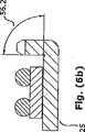
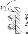
突起部を90度に曲げることは困難である。リードフレームの金属は一定の反発力を有し、曲げ工程において反発する傾向がある。そのため、対策としては、少なくとも90度までの範囲でわずかに曲げを行うことである。好適な実施例では、わずかな曲げは90度までであることが好ましい。図6(b)の角度56.2を参照されたい。製造における6段階ある自由度として、角度は図6(a)の角度56.1によって示される95度と、図6(c)の角度56.3によって示される85度の間でもよい。 It is difficult to bend the protrusion at 90 degrees. The metal of the lead frame has a certain repulsive force and tends to repel during the bending process. Therefore, a countermeasure is to perform a slight bending within a range of at least 90 degrees. In the preferred embodiment, the slight bend is preferably up to 90 degrees. See angle 56.2 in FIG. 6 (b). As 6 degrees of freedom in manufacturing, the angle may be between 95 degrees as indicated by angle 56.1 in FIG. 6 (a) and 85 degrees as indicated by angle 56.3 in FIG. 6 (c).
図1を参照すると最後のステップ25は、曲げステップである。このステップの一部として、台形状先端部36の端部65は、残ったばりを除去し、共通平面上にある突起部の端部を調整するために軽く叩かれる。叩くことは非常に制御された工程である。それは、直立した突起部に過剰な応力を加えるものではない。しかしながら、仮に、叩いている間に突起部が曲がってしまいがちあるならば、叩いている間、突起部の少なくとも反対側の2箇所の側面で支持部を設けて突起部を支持することは当業者には周知である。これら支持部(図示しない)は、突起部のゆがみを減少もしくは防止する。 Referring to FIG. 1, the
本発明は、突起部が形成されるDAP30の1つ、2つ、3つの縁部で使用してもよい。突起部を備えた4縁部を形成することが可能である。しかしながら、突起部を備えた縁部の目的は、半導体ダイ60の底部にある電極へ電気的な接続を設けるためであることを覚えておかなければならない。本願のほぼ全てにおいて、これら突起部を備えた3つの縁部は、ダイ60の裏側へ良好な電気的接続を設けるのに十分である。本願の多くの場合、突起部を備えた1つの縁部で十分である。次の説明は、突起部を備えた3つの縁部を有するパッケージと突起部を備えた1つの縁部を有するパッケージを作成するための本発明の使用方法を説明している。突起部を備えた2つの縁部を有するパッケージは3面法を用いて作成され、1つの面の上に1の縁部を形成しない。また、1つの縁部を有するパッケージに処理を施し、突起部を備えた第2の縁部を形成する。 The present invention may be used at one, two, three edges of the
図3.1−3.4を参照すると、1つ以上のDAP30を備えたリードフレーム70を有する発明の1つの実施例を示されている。各DAP30は曲げられた突起部36を備えた3つの縁部を有する。DAP30はサイドレール71、72に接続されている。1対のタイバー73、74は、DAP30の2つの角をサイドレール72へ接続している。縁部30.1とサイドレール72の間にある空間に注意されたい。反対側にある縁部30.4は、一方のサイドレール71に対し同じ広がりを有する。サイドレール71と72の間にあるDAP30の態様はDAP30の連続として繰り返され、リードフレーム70に6個以上のDAP30を1対のサイドレール71、72の間に設けてもよい。半導体デバイス60は、DAP30の中心部分31に付加される。半導体デバイス60の表面部65は共通接続を有する。一般的な共通接続は、MOSFETのドレインまたはバイポーラトランジスタのコレクタである。デバイス60の他の表面は、ボールのアレイもしくは突起部61を有する。MOSFETの場合、ボールの大部分または突起部はソース領域に接続されており、少なくとも1つのボールまたは突起部がゲートに接続されている。バイポーラデバイスでは、ボールの大部分または突起部はエミッタ領域に接続され、少なくとも1つのボールまたは突起部がデバイス60の表面部にあるベース領域に接続されている。 Referring to FIGS. 3.1-3.4, one embodiment of the invention having a
図3.2は、図3.1と一致する部分図であるが、サイドレールは示されていない。図3.3に示されている次のステップでは、残りのDAPとデバイス60は輪郭図80の中にある。次のステップでは、適切な加工機械がサイドレール72からタイバー73、74を切断する。そして、DAP30からサイドレール71の余分な部分を切断して、図3.4に示されているデバイス60を備える切り出されたDAP30を残す。切り出されたDAP30とデバイス60は、回路基板上で反転して集積するための準備がなされるか、または、個別にパッケージングしてもよい。 FIG. 3.2 is a partial view consistent with FIG. 3.1, but the side rails are not shown. In the next step shown in FIG. 3.3, the remaining DAP and
図4(a)−4(b)を参照すると、従来の技術によってリードフレーム103上の片側バンプを、本発明によって他のリードフレーム70.1上に突起部を片側に備えた縁部を有するパッケージと比較している。従来技術の組合せは、DAP104と、DAP104の1つの縁部上にパンチングされたバンプ60を有している。従来技術のデバイスは、必須のレールと連続したDAP104の間にある空間を有し、DAPは互いに離れている。本発明によるパッケージは2つの異なったサイドレール71.1と72.1を有しており、DAP30は、2つのレールの間に広がっており4本のタイバーによって支持されている。ダイがDAP30に付加された後、切り出し加工を行う機械は、サイドレール71.1と72.1の間にあるタイバーとDAP30を切断する。その後、回収と設置を行う機械がDAP30を回収し、プリント回路基板へ半田付けするための適切な場所にDAP30を設置する。 Referring to FIGS. 4 (a) -4 (b), one-sided bumps on the
ダイ314と単一面の台形状突起部を備えた縁部310を有する曲げを完了したフレーム300は、図7(a) と7(b)に示されている。曲げられた突起部を備えた壁301は約1.45mmの幅を有し、パッケージ幅311全体は約1.550 mmである。半田ペースト構造302は、ダイパッド325の上でダイ360を保持する。パッケージ300は約1.550mmの長さ303を有する。ダイパッド314の長さ308は約1.25 mmである。突起部の端部のDAP表面部までの距離は約0.42mmであり、パッケージ321の全体の高さは約0.67mmである。突起部の端部は約0.05mmの半径313を有する。半田バンプ315は、約300μmの直径を有する。パッケージ全体の高さ317は約0.71mmである。ダイ314とボールグリッドアレイを合わせた高さは約0.46mmである。 A completed
一般的に、図5(a)と図5(b)中の1つに示されるように、より小さなダイでは1つの縁部を曲げたパッケージで十分である。しかし、より大きなサイズのダイではしばしば、2つまたは3つの縁部を曲げた壁を要求し、回路基板に対するダイ後部電極の確実な電気的接続と、曲げられたパッケージの確実で機械的な接続を設ける。 In general, as shown in one of FIGS. 5 (a) and 5 (b), a package with one edge bent is sufficient for smaller dies. However, larger dies often require walls with two or three edge bends to ensure reliable electrical connection of the die back electrode to the circuit board and reliable mechanical connection of the bent package. Is provided.
従来技術のパッケージを生産するために用いられるスタンピング方法、鋳造方法、パンチング方法と比較すると、本発明の方法と装置は経済的利点に優れている。次の説明では、従来技術の工程と本発明で示される装置を比較する。 Compared to the stamping, casting, and punching methods used to produce prior art packages, the method and apparatus of the present invention have excellent economic advantages. In the following description, the prior art process and the apparatus shown in the present invention are compared.
一般的な従来技術のスタンピング工程を図10に示す。スタンピング装置は、多重スタンピング材料を有するスタンピング機械(しばしば、スタンピングツールと呼ばれる。図示しない)と、対応するスタンピングダイ120を含む。スタンピングダイは、多重スタンピング材料を受けるために構成される凹部を有する。一般的な工程では、金属層100はスタンピングダイに設置される。スタンピング材料は、金属層がスタンピングダイに置かれている間、金属層をパンチングする。パンチングの間、スタンピング材料は、金属層の間を通過することなしにスタンピングダイの凹部にある金属層の部分を押す。金属層に適用される圧力は金属層の部分を変形させ、金属層中の多重に押されたバンプを形成する。このスタンピング工程は繰り返され、バンプの集団が形成される。特に、従来技術のリードフレーム100は2つの寸法を有しており、101部分は突起部分として約0.75mmであり、102部分は最終ダイパッドの厚みとして約0.33mmである。0.75mm部分は巧妙に鋳造され、厚さ0.33mmのダイパッド部分と独自の厚さのエッジ部分102を形成する。次に、より厚い部分101はパンチングされてリードフレームのより厚い部分101の表面から上に突き出たコニカルサッド104を形成する。これにより最終生成物109を形成する。 A general prior art stamping process is shown in FIG. The stamping device includes a stamping machine (often referred to as a stamping tool, not shown) having multiple stamping materials and a corresponding stamping die 120. The stamping die has a recess configured to receive multiple stamping materials. In a typical process, the
対照的に、本発明を0.75mm未満や0.25mmと同程度に薄いリードフレームで始めてもよい。発明はこのように、リードフレーム全体に均一な厚みと、より少ない材料ですむことを提供する。従来技術と本発明の双方において対応するリードフレームでは、本発明は従来技術により必要とされる材料の3分の1だけでよい。材料費だけで、本発明は材料費を66%削減する。1つのパッケージ各々の材料費が非常に少ない半面、小規模な生産によって毎年典型的に生産されることにより材料費が増加すれば、生産者にとってコスト削減は非常に重要である。 In contrast, the present invention may begin with a lead frame that is less than 0.75 mm or as thin as 0.25 mm. The invention thus provides for a uniform thickness and less material throughout the lead frame. With lead frames that are compatible in both the prior art and the present invention, the present invention requires only one third of the material required by the prior art. With only material costs, the present invention reduces material costs by 66%. While the material cost of each package is very low, cost reduction is very important for the producer if the material cost increases by being typically produced every year by small production.
本発明ではまた、製造がより容易である。従来技術のリードフレームで実行される製造工程は、数トンもの製造装置とスタンピング装置を必要とする。対照的に、軽い重量の、加工と形成を行う機械は、本発明による曲げられたリードフレームを形成するのに十分である。 The present invention is also easier to manufacture. The manufacturing process performed with the prior art lead frame requires several tons of manufacturing equipment and stamping equipment. In contrast, a light weight processing and forming machine is sufficient to form a bent lead frame according to the present invention.
本発明の他の利点は、ダイパッドが押されないこと、または、薄くしたり接触しないことである。シングルゲージ材料の使用は、従来技術のデバイスよりも、さらに強固で、より完成度が高く集積された半導体デバイスを設ける。対照的に、従来技術の変形は従来技術におけるリードフレームの相対的に大きな領域を変形し、縁部にある突起部よりも薄いダイパッドを形成する。従来技術のダイパッドのスタンピングと鋳造はパッドを破壊するかもしれない。 Another advantage of the present invention is that the die pad is not pushed or thinned or touched. The use of single gauge materials provides a more robust and more complete integrated semiconductor device than prior art devices. In contrast, prior art deformations deform a relatively large area of the lead frame in the prior art, forming a die pad that is thinner than the protrusions at the edges. Prior art die pad stamping and casting may destroy the pad.
我々は、スタンピングと鋳造がダイパッド材料内で内部応力をかけることを確信している。さらに先の工程または試験ステップの間、リードフレームには加熱や冷却がなされ、そして、それにより内部の応力を開放することができる。その応力を解放する時、ダイがダイパッドから離れるかもしれない。いくつかの失敗した部品の分析では、ダイが割れたり、またはダイパッドから持ち上がるということが示された。スタンピングと鋳造による内部の構造的な応力は、ダイパッドが伸張/収縮し、それゆえダイがダイパッドで壊れる原因となる。対照的に、本発明は、ダイパッドの鋳造やスタンピングを行わないので、ダイパッドには不要な応力がかからない。本発明が用いられる場合、ダイパッドからダイが持ち上がることは、実質的にない。 We are confident that stamping and casting will apply internal stresses in the die pad material. Furthermore, during the previous process or test step, the lead frame can be heated and cooled, thereby relieving internal stress. When releasing the stress, the die may move away from the die pad. Analysis of several failed parts showed that the die cracked or lifted off the die pad. Internal structural stresses due to stamping and casting cause the die pad to stretch / shrink and thus cause the die to break at the die pad. In contrast, the present invention does not cast or stamp the die pad, so that no unnecessary stress is applied to the die pad. When the present invention is used, there is virtually no lifting of the die from the die pad.
タイバーがダイパッドから切り離される時、先行技術のデュアルゲージリードフレームには問題ある。なぜなら、タイバーはダイパッドより厚いからであり、タイバーを切断するステップは、ダイパッド上でねじれ力を与える。なぜなら、ダイパッドはタイバーよりも薄いので、ダイパッドはねじれやすく、そのねじれがダイパッドを破壊したり、またはダイパッドからダイが分離したりする可能性がある。対照的に、本発明のシングルゲージリードフレームは、そのようなねじれ力とねじれを有しない。なぜならば、リードフレームのすべての部分は同じゲージだからである。 Prior art dual gauge lead frames are problematic when the tie bar is disconnected from the die pad. This is because the tie bar is thicker than the die pad, and the step of cutting the tie bar provides a twisting force on the die pad. Because the die pad is thinner than the tie bar, the die pad is easily twisted, and the twist may break the die pad or cause the die to separate from the die pad. In contrast, the single gauge lead frame of the present invention does not have such a twisting force and twist. This is because all parts of the lead frame are the same gauge.
シングルゲージリードフレームを形成するよりもデュアルゲージリードフレームを形成することの方が困難である。本発明のシングルゲージリードフレームはより薄い突起部を備えた縁部を有する。このように、本発明は、従来技術が形成することができるよりも縁部に沿ってより多くの突起部を形成することができる。なぜならば、発明の突起部は、それらの端部のみから加工され形成されたからである。対照的に、従来技術の突起部は、金属をダイキャビティにスタンピング込むことによって形成される。その技術により、縁部の先端部間の配置または間隔に関する技術は、金属の破壊を防ぐために必要な支持部によって制限される。 It is more difficult to form a dual gauge lead frame than to form a single gauge lead frame. The single gauge lead frame of the present invention has an edge with a thinner protrusion. Thus, the present invention can form more protrusions along the edge than the prior art can form. This is because the protrusions of the invention are processed and formed only from their end portions. In contrast, prior art protrusions are formed by stamping metal into the die cavity. With that technique, the technique regarding the placement or spacing between the edge tips is limited by the support necessary to prevent metal breakdown.
本発明のもう一つの長所は、最低限の複雑さで、1つ、2つ、3つの縁部上に突起部を形成が可能であることである。主要な金属加工工程は材料除去と非変形であるため、本発明の工程は、ディープダイキャビティと金属の破壊から保護するための大きな支持部を必要としない。その上、本発明は金属を除去して突起部を形成し、そして、さらに多くの金属を除去して曲げステップの準備を行う。突起部の先端部のみが加工され、そして、台形状先端部に形成される。金属が水平状態にある間、本発明での金属は加工されるに過ぎない。対照的に、従来技術は金属変形を用いて、金属を1つの平面から金属平面に垂直な平面へスタンピング出すことによって突起部全体を形成する。 Another advantage of the present invention is that protrusions can be formed on one, two, or three edges with minimal complexity. Since the main metalworking processes are material removal and non-deformation, the process of the present invention does not require large supports to protect against deep die cavities and metal breakdown. In addition, the present invention removes metal to form protrusions, and removes more metal to prepare for the bending step. Only the tip of the projection is processed and formed into a trapezoidal tip. While the metal is in a horizontal state, the metal in the present invention is only processed. In contrast, the prior art uses metal deformation to form the entire protrusion by stamping the metal from one plane to a plane perpendicular to the metal plane.
本発明によって、突起部バンプを2つまたは3つの縁部へ容易に伸張させることができ、タイバーを直接に除去することができる。なぜならば、リードフレームの全ての材料は同じゲージを有しているからである。しかしながら、従来技術のリードフレームは、突起部を備えた縁部のために厚いゲージを有している。厚いゲージを有しているということは、2つまたは3つの縁部に突起部を備えることが非常に困難であることになる。従来技術の縁部は、厚さ0.75mmであり、縁部方向へのタイバーは類似の厚みを有することに留意されたい。そのようなタイバーは、切断や加工するのが困難である。 According to the present invention, the protrusion bump can be easily extended to two or three edges, and the tie bar can be directly removed. This is because all the materials of the lead frame have the same gauge. However, the prior art lead frame has a thick gauge due to the edge with the protrusion. Having a thick gauge makes it very difficult to have protrusions on two or three edges. Note that the prior art edge is 0.75 mm thick and the tie bars in the edge direction have a similar thickness. Such tie bars are difficult to cut or process.
Claims (26)
Translated fromJapanese前記半導体ダイを受けて保持するための平坦部を有するリードフレームを設けるステップと、
前記リードフレームの前記平坦部の第1の縁部に沿った1つ以上の突起部を形成するステップと、
前記平坦部表面上に、前記第1の縁部と平行に配され、前記第1の縁部から離れた1の溝を形成するステップと、
前記1つ以上の突起部の各々の端部に4つの傾斜面を有する先端部を形成するステップと、
前記第1の縁部を、前記リードフレームの前記平坦部に対し前記溝のまわりに1の角度まで曲げるステップと、を有することを特徴とする方法。A method of packaging a semiconductor die, comprising:
Providing a lead frame having a flat portion for receiving and holding the semiconductor die;
Forming one or more protrusions along a first edge of the flat portion of the lead frame;
Forming, on the surface of the flat part, one groove disposed in parallel with the first edge and spaced from the first edge;
Forming a tip having four inclined surfaces at each end of the one or more protrusions;
Bending the first edge to the flat angle of the lead frame around the groove to an angle of one.
前記半導体ダイの前記ダイ取り付け表面部を前記リードフレームの平面部に取り付けて、ボールグリッドアレイを前記リードフレームの平面部から向きをそらすステップと、をさらに含み、
前記1つ以上の突起部の各々の前記先端部が、前記半導体ダイの前記表面部上に配された前記ボールアレイと同一面になるように、前記溝が形成され且つ前記リードフレームの前記第1の縁部が曲げられることを特徴とする請求項1記載の方法。Providing a semiconductor die with a die attach surface and a ball grid array surface;
Attaching the die attach surface portion of the semiconductor die to the planar portion of the lead frame and diverting the ball grid array from the planar portion of the lead frame;
The groove is formed so that the tip of each of the one or more protrusions is flush with the ball array disposed on the surface portion of the semiconductor die, and the first portion of the lead frame is formed. 2. A method according to claim 1, characterized in that one edge is bent.
1つの電極のみを備えた前記表面部に平坦な接続部を形成して前記他の表面部にボールグリッドアレイの接続部を形成するステップと、
前記半導体ダイの前記平坦な接続部を前記リードフレームの前記平坦部へ取り付けるステップと、をさらに含み、
前記1つ以上の突起部の各々の前記先端部が、前記ボールアレイと同一面になるように、前記溝が形成され且つ前記リードフレームの前記第1の縁部が曲げられることを特徴とする請求項1記載の方法。Providing a semiconductor die with only one electrode on one surface and one or more electrodes on the other surface;
Forming a flat connection portion on the surface portion including only one electrode and forming a connection portion of a ball grid array on the other surface portion; and
Attaching the flat connection portion of the semiconductor die to the flat portion of the lead frame;
The groove is formed and the first edge of the lead frame is bent so that the tip of each of the one or more protrusions is flush with the ball array. The method of claim 1.
前記平坦部表面上に、前記第2の縁部と平行に配され、前記第2の縁部から離れた第2の溝を形成するステップと、
前記第2の縁部を前記リードフレームの前記平坦部に対して1の角度まで曲げるステップと、をさらに有することを特徴とする請求項1記載の方法。Forming one or more protrusions along a second edge of the flat portion of the lead frame;
Forming a second groove on the surface of the flat portion, parallel to the second edge and away from the second edge;
The method of claim 1, further comprising bending the second edge to an angle of 1 with respect to the flat portion of the lead frame.
前記平坦部の表面上に、前記第3の縁部と平行に配され、前記第3の縁部から離れた第3の溝を形成するステップと、
前記第3の縁部を前記リードフレームの前記平坦部に対し1の角度まで曲げるステップと、をさらに有することを特徴とする請求項9記載の方法。Forming one or more protrusions along a third edge of the flat portion of the lead frame;
Forming a third groove on the surface of the flat portion in parallel with the third edge and away from the third edge;
10. The method of claim 9, further comprising bending the third edge to an angle of 1 with respect to the flat portion of the lead frame.
半導体ダイを受ける平坦部を有するダイ取り付けパッドと、
前記平坦部上にあり、半導体ダイを保持する接着層または半田層と、
接着層または半田によって、前記ダイ取り付けパッドの前記平坦部に面して取り付けられた1つの表面部を有する半導体ダイと、
前記ダイ取り付けパッドの1つの縁部に沿って、前記ダイ取り付けパッドに対して横向きに配された壁と、
前記壁から伸張し、互いに間隔をおいて配された複数の突起部と、を含み、
前記突起部の端部は、4つの傾斜面を有する台形のテ―パ状の端部を有することを特徴とするフリップチップ・パッケージングされた半導体デバイス。A flip chip packaged semiconductor device comprising:
A die attach pad having a flat portion for receiving a semiconductor die;
An adhesive layer or a solder layer on the flat portion and holding the semiconductor die;
A semiconductor die having one surface portion attached to the flat portion of the die attachment pad by an adhesive layer or solder;
A wall disposed transversely to the die attach pad along one edge of the die attach pad;
A plurality of protrusions extending from the wall and spaced apart from each other,
The flip chip packaged semiconductor device is characterized in that the end of the protrusion has a trapezoidal taper end having four inclined surfaces.
半導体ダイと1つ以上の縁部を受ける平坦部を有するダイ取り付けパッドと、
前記平坦部上で、半導体ダイを保持する接着層または半田層と、
接着層または半田によって前記ダイ取り付けパッドの前記平坦部に面して取り付けられる1つの表面部を有し、他の表面部がバンプまたはボール接着を備えた半導体ダイと、
各壁が前記ダイ取り付けパッドの縁部に沿っていて前記ダイ取り付けパッドに対して横向きに配されている1つ以上の壁と、
前記1つ以上の壁の各々から伸張する複数の離間した突起部と、を有し、
前記複数の離間した突起部の各々の端部は、4つの傾斜面を有する台形のテ―パ状の端部を有することを特徴とするフリップチップ・パッケージングされた半導体デバイス。A flip chip packaged semiconductor device comprising:
A die attach pad having a semiconductor die and a flat portion for receiving one or more edges;
An adhesive layer or a solder layer for holding a semiconductor die on the flat portion;
A semiconductor die having one surface portion attached to the flat portion of the die attachment pad by an adhesive layer or solder and the other surface portion having a bump or ball adhesion;
One or more walls, each wall being disposed transversely to the die attach pad along an edge of the die attach pad;
A plurality of spaced protrusions extending from each of the one or more walls,
A flip-chip packaged semiconductor device, wherein each of the plurality of spaced projections has a trapezoidal taper-shaped end having four inclined surfaces.
前記半導体ダイを受けて保持する平坦なダイ取り付けパッドを備えたリードフレームを設けるステップと、
前記ダイ取り付けパッドの1つ以上の縁部に突起部をパンチングして、縁部から突き出た1つ以上の突起部を形成するステップと、
パンチングされた各縁部の近傍において、前記ダイ取り付けパッドの前記表面部に溝を形成するステップと、
前記1つ以上の突起部の各々の端部に4つの傾斜面を有する先端部を形成するステップと、
形成された溝に対してパンチングされた縁部を2つの別々の工程により溝の方向へ曲げて、突起部を備えた前記パンチングされた縁部をダイ取り付けパッドに対して1の角度に配するステップと、を有することを特徴とする半導体ダイをパッケージングする方法。A method of packaging a semiconductor die, comprising:
Providing a lead frame with a flat die attach pad for receiving and holding the semiconductor die;
Punching protrusions on one or more edges of the die attach pad to form one or more protrusions protruding from the edges;
Forming a groove in the surface portion of the die attachment pad in the vicinity of each punched edge; and
Forming a tip having four inclined surfaces at each end of the one or more protrusions;
The punched edge with respect to the formed groove is bent in the direction of the groove in two separate steps, and the punched edge with protrusions is placed at an angle with respect to the die attach pad. And a method of packaging a semiconductor die.
前記半導体ダイの前記平坦な表面部を前記平坦なダイ取り付けパッドへ接続するステップと、
前記突起部の前記端部が前記半導体表面のバンプの端部が同一面になるようにまで、突起部を備えるパンチングされた前記縁部の各々を溝に対して平行な軸のまわりに曲げるステップと、を有することを特徴とする請求項23記載の方法。Providing a semiconductor die having a flat portion on one surface with flat connection portions and an opposite surface portion with bump connection portions;
Connecting the flat surface portion of the semiconductor die to the flat die attach pad;
Bending each of the punched edges with protrusions about an axis parallel to the groove until the ends of the protrusions are flush with bump ends on the semiconductor surface 24. The method of claim 23, comprising:
前記半導体ダイを受けて保持する平坦部を備えたリードフレームを設けるステップと、
前記リードフレームの前記平坦部の1つの縁部に沿って突起部を形成するステップと、
前記突起部の端部に4つの傾斜面を有する先端部を形成するステップと、
前記突起部を有する前記縁部に平行に設けられ且つ前記縁部から離間された前記平坦部の表面部に溝を形成するステップと、
前記縁部を、前記リードフレームの前記平坦部に対し前記溝のまわりに1の角度まで曲げるステップと、
前記突起部の端部を叩くステップと、を含む半導体ダイをパッケージングする方法。A method of packaging a semiconductor die, comprising:
Providing a lead frame with a flat portion for receiving and holding the semiconductor die;
Forming a protrusion along one edge of the flat portion of the lead frame;
Forming a tip having four inclined surfaces at an end of the protrusion;
Forming a groove in a surface portion of the flat portion provided in parallel to the edge portion having the protrusion and spaced from the edge portion;
Bending the edge to an angle of 1 around the groove relative to the flat portion of the lead frame;
Tapping an end of the protrusion, and packaging the semiconductor die.
前記半導体ダイの前記平坦な表面部を前記平坦なダイ取り付けパッドへ接続するステップと、
前記突起部の前記端部が前記半導体表面のバンプの端部が同一面になるようにまで、突起部を備えるパンチングされた前記縁部の各々を溝に対して平行な軸のまわりに曲げるステップと、を有することを特徴とする請求項25記載の方法。Providing a semiconductor die having a flat portion on one surface with flat connection portions and an opposite surface portion with bump connection portions;
Connecting the flat surface portion of the semiconductor die to the flat die attach pad;
Bending each of the punched edges with protrusions about an axis parallel to the groove until the ends of the protrusions are flush with bump ends on the semiconductor surface 26. The method of claim 25, comprising:
Applications Claiming Priority (3)
| Application Number | Priority Date | Filing Date | Title |
|---|---|---|---|
| US11/179,348US7402462B2 (en) | 2005-07-12 | 2005-07-12 | Folded frame carrier for MOSFET BGA |
| US11/179,348 | 2005-07-12 | ||
| PCT/US2006/027167WO2007009024A2 (en) | 2005-07-12 | 2006-07-12 | Folded frame carrier for mosfet bga |
Publications (2)
| Publication Number | Publication Date |
|---|---|
| JP2009502026A JP2009502026A (en) | 2009-01-22 |
| JP4903205B2true JP4903205B2 (en) | 2012-03-28 |
Family
ID=37637955
Family Applications (1)
| Application Number | Title | Priority Date | Filing Date |
|---|---|---|---|
| JP2008521595AExpired - Fee RelatedJP4903205B2 (en) | 2005-07-12 | 2006-07-12 | Flip-chip packaged semiconductor device and method for packaging a semiconductor die |
Country Status (7)
| Country | Link |
|---|---|
| US (1) | US7402462B2 (en) |
| JP (1) | JP4903205B2 (en) |
| KR (1) | KR101321190B1 (en) |
| CN (1) | CN101553908B (en) |
| DE (1) | DE112006001866T5 (en) |
| TW (1) | TWI395301B (en) |
| WO (1) | WO2007009024A2 (en) |
Families Citing this family (8)
| Publication number | Priority date | Publication date | Assignee | Title |
|---|---|---|---|---|
| JP4977378B2 (en)* | 2006-02-23 | 2012-07-18 | 山梨日本電気株式会社 | Magnetic sensor, rotation detection device, and position detection device |
| US20090166826A1 (en)* | 2007-12-27 | 2009-07-02 | Janducayan Omar A | Lead frame die attach paddles with sloped walls and backside grooves suitable for leadless packages |
| US7855439B2 (en)* | 2008-08-28 | 2010-12-21 | Fairchild Semiconductor Corporation | Molded ultra thin semiconductor die packages, systems using the same, and methods of making the same |
| US7829988B2 (en)* | 2008-09-22 | 2010-11-09 | Fairchild Semiconductor Corporation | Stacking quad pre-molded component packages, systems using the same, and methods of making the same |
| US8314499B2 (en)* | 2008-11-14 | 2012-11-20 | Fairchild Semiconductor Corporation | Flexible and stackable semiconductor die packages having thin patterned conductive layers |
| JP2015065270A (en) | 2013-09-25 | 2015-04-09 | ソニー株式会社 | Solid state image pickup device and manufacturing method of the same, and electronic apparatus |
| JP6210818B2 (en)* | 2013-09-30 | 2017-10-11 | 三菱電機株式会社 | Semiconductor device and manufacturing method thereof |
| CN115939074B (en)* | 2023-03-13 | 2023-08-22 | 新恒汇电子股份有限公司 | Novel double-sided flexible lead frame structure and preparation process thereof |
Family Cites Families (13)
| Publication number | Priority date | Publication date | Assignee | Title |
|---|---|---|---|---|
| US6133634A (en) | 1998-08-05 | 2000-10-17 | Fairchild Semiconductor Corporation | High performance flip chip package |
| JP3851760B2 (en)* | 2000-07-04 | 2006-11-29 | 松下電器産業株式会社 | Semiconductor device, mounting method thereof, manufacturing method of electronic circuit device, and electronic circuit device manufactured by the manufacturing method |
| JP2002270751A (en)* | 2001-03-13 | 2002-09-20 | Fujitsu Denso Ltd | Lead terminal, lead frame and electronic component |
| US6893901B2 (en) | 2001-05-14 | 2005-05-17 | Fairchild Semiconductor Corporation | Carrier with metal bumps for semiconductor die packages |
| JP3868777B2 (en)* | 2001-09-11 | 2007-01-17 | 株式会社東芝 | Semiconductor device |
| US7122884B2 (en)* | 2002-04-16 | 2006-10-17 | Fairchild Semiconductor Corporation | Robust leaded molded packages and methods for forming the same |
| JP3853263B2 (en)* | 2002-07-08 | 2006-12-06 | Necエレクトロニクス株式会社 | Semiconductor device |
| US6860741B2 (en)* | 2002-07-30 | 2005-03-01 | Avx Corporation | Apparatus and methods for retaining and placing electrical components |
| EP1527479A1 (en)* | 2002-08-05 | 2005-05-04 | Osram Opto Semiconductors GmbH | Method for the production of an electrically-conducting frame, method for production of a surface mounting semiconductor component and conductor frame strips |
| JP3757212B2 (en)* | 2003-03-14 | 2006-03-22 | 東光株式会社 | Semiconductor device |
| JP4248928B2 (en)* | 2003-05-13 | 2009-04-02 | ローム株式会社 | Semiconductor chip manufacturing method, semiconductor device manufacturing method, semiconductor chip, and semiconductor device |
| TWI274406B (en)* | 2003-07-16 | 2007-02-21 | Freescale Semiconductor Inc | Dual gauge leadframe |
| TWI224841B (en)* | 2003-08-20 | 2004-12-01 | Chipmos Technologies Inc | Film ball grid array package structure of an image sensor |
- 2005
- 2005-07-12USUS11/179,348patent/US7402462B2/ennot_activeExpired - Fee Related
- 2006
- 2006-07-11TWTW095125352Apatent/TWI395301B/ennot_activeIP Right Cessation
- 2006-07-12JPJP2008521595Apatent/JP4903205B2/ennot_activeExpired - Fee Related
- 2006-07-12CNCN2006800332195Apatent/CN101553908B/ennot_activeExpired - Fee Related
- 2006-07-12WOPCT/US2006/027167patent/WO2007009024A2/enactiveApplication Filing
- 2006-07-12KRKR1020087000712Apatent/KR101321190B1/ennot_activeExpired - Fee Related
- 2006-07-12DEDE112006001866Tpatent/DE112006001866T5/ennot_activeWithdrawn
Also Published As
| Publication number | Publication date |
|---|---|
| TWI395301B (en) | 2013-05-01 |
| US20070015316A1 (en) | 2007-01-18 |
| WO2007009024A2 (en) | 2007-01-18 |
| CN101553908B (en) | 2012-06-13 |
| JP2009502026A (en) | 2009-01-22 |
| US7402462B2 (en) | 2008-07-22 |
| KR101321190B1 (en) | 2013-10-23 |
| DE112006001866T5 (en) | 2008-05-15 |
| TW200713526A (en) | 2007-04-01 |
| WO2007009024A3 (en) | 2009-04-09 |
| CN101553908A (en) | 2009-10-07 |
| KR20080031270A (en) | 2008-04-08 |
Similar Documents
| Publication | Publication Date | Title |
|---|---|---|
| JP4903205B2 (en) | Flip-chip packaged semiconductor device and method for packaging a semiconductor die | |
| EP2963684A1 (en) | Power semiconductor device | |
| JP3853263B2 (en) | Semiconductor device | |
| US10297535B2 (en) | Die package component with jumper structure and manufacturing method thereof | |
| JP3776427B2 (en) | Semiconductor device and manufacturing method thereof | |
| KR100721279B1 (en) | A method of forming a semiconductor chip assembly and an apparatus for forming a wire bond portion from a circuit on a substrate to a semiconductor chip | |
| US7534661B2 (en) | Method of forming molded resin semiconductor device | |
| JP2005158883A (en) | Circuit board | |
| JPH08148623A (en) | Semiconductor device | |
| EP0204102A2 (en) | Direct connection of lead frame having flexible, tapered leads and mechanical die support | |
| US11817374B2 (en) | Electronic device with exposed tie bar | |
| KR100721274B1 (en) | Method of Forming Semiconductor Chip Assembly | |
| TWI250581B (en) | Three dimension package and method for manufacturing the same | |
| JP2006261448A (en) | Semiconductor device and manufacturing method of semiconductor device | |
| JP2013048150A (en) | Semiconductor module and manufacturing method of the same | |
| JP2003175493A (en) | Stamping die | |
| JP2005072190A (en) | Semiconductor device and method for manufacturing same | |
| JP2000232185A (en) | Printed wiring board for semiconductor package, semiconductor package, and method of manufacturing semiconductor package | |
| JPH0917938A (en) | Fixed structure of semiconductor chip and method of manufacturing semiconductor device | |
| JPH09252063A (en) | Lead frame, semiconductor integrated circuit device using the same, and method of manufacturing the same | |
| JP2015043465A (en) | Semiconductor device | |
| JP2006196927A (en) | Semiconductor device | |
| JPH06132350A (en) | Semiconductor device | |
| JP2001007273A (en) | Semiconductor device and method of manufacturing the same |
Legal Events
| Date | Code | Title | Description |
|---|---|---|---|
| A621 | Written request for application examination | Free format text:JAPANESE INTERMEDIATE CODE: A621 Effective date:20090615 | |
| A977 | Report on retrieval | Free format text:JAPANESE INTERMEDIATE CODE: A971007 Effective date:20100212 | |
| A131 | Notification of reasons for refusal | Free format text:JAPANESE INTERMEDIATE CODE: A131 Effective date:20110308 | |
| A521 | Request for written amendment filed | Free format text:JAPANESE INTERMEDIATE CODE: A523 Effective date:20110607 | |
| A131 | Notification of reasons for refusal | Free format text:JAPANESE INTERMEDIATE CODE: A131 Effective date:20110712 | |
| A521 | Request for written amendment filed | Free format text:JAPANESE INTERMEDIATE CODE: A523 Effective date:20111007 | |
| A131 | Notification of reasons for refusal | Free format text:JAPANESE INTERMEDIATE CODE: A131 Effective date:20111101 | |
| A521 | Request for written amendment filed | Free format text:JAPANESE INTERMEDIATE CODE: A523 Effective date:20111108 | |
| TRDD | Decision of grant or rejection written | ||
| A01 | Written decision to grant a patent or to grant a registration (utility model) | Free format text:JAPANESE INTERMEDIATE CODE: A01 Effective date:20111213 | |
| A01 | Written decision to grant a patent or to grant a registration (utility model) | Free format text:JAPANESE INTERMEDIATE CODE: A01 | |
| A61 | First payment of annual fees (during grant procedure) | Free format text:JAPANESE INTERMEDIATE CODE: A61 Effective date:20120104 | |
| R150 | Certificate of patent or registration of utility model | Free format text:JAPANESE INTERMEDIATE CODE: R150 | |
| FPAY | Renewal fee payment (event date is renewal date of database) | Free format text:PAYMENT UNTIL: 20150113 Year of fee payment:3 | |
| LAPS | Cancellation because of no payment of annual fees |