JP4900572B2 - 2D photonic crystal - Google Patents
2D photonic crystalDownload PDFInfo
- Publication number
- JP4900572B2 JP4900572B2JP2006077600AJP2006077600AJP4900572B2JP 4900572 B2JP4900572 B2JP 4900572B2JP 2006077600 AJP2006077600 AJP 2006077600AJP 2006077600 AJP2006077600 AJP 2006077600AJP 4900572 B2JP4900572 B2JP 4900572B2
- Authority
- JP
- Japan
- Prior art keywords
- photonic crystal
- dimensional photonic
- refractive index
- lattice
- main body
- Prior art date
- Legal status (The legal status is an assumption and is not a legal conclusion. Google has not performed a legal analysis and makes no representation as to the accuracy of the status listed.)
- Expired - Fee Related
Links
Images


Classifications
- G—PHYSICS
- G02—OPTICS
- G02B—OPTICAL ELEMENTS, SYSTEMS OR APPARATUS
- G02B6/00—Light guides; Structural details of arrangements comprising light guides and other optical elements, e.g. couplings
- G02B6/10—Light guides; Structural details of arrangements comprising light guides and other optical elements, e.g. couplings of the optical waveguide type
- G02B6/12—Light guides; Structural details of arrangements comprising light guides and other optical elements, e.g. couplings of the optical waveguide type of the integrated circuit kind
- G02B6/122—Basic optical elements, e.g. light-guiding paths
- G02B6/1225—Basic optical elements, e.g. light-guiding paths comprising photonic band-gap structures or photonic lattices
- B—PERFORMING OPERATIONS; TRANSPORTING
- B82—NANOTECHNOLOGY
- B82Y—SPECIFIC USES OR APPLICATIONS OF NANOSTRUCTURES; MEASUREMENT OR ANALYSIS OF NANOSTRUCTURES; MANUFACTURE OR TREATMENT OF NANOSTRUCTURES
- B82Y20/00—Nanooptics, e.g. quantum optics or photonic crystals
- G—PHYSICS
- G02—OPTICS
- G02B—OPTICAL ELEMENTS, SYSTEMS OR APPARATUS
- G02B6/00—Light guides; Structural details of arrangements comprising light guides and other optical elements, e.g. couplings
- G02B6/10—Light guides; Structural details of arrangements comprising light guides and other optical elements, e.g. couplings of the optical waveguide type
- G02B6/12—Light guides; Structural details of arrangements comprising light guides and other optical elements, e.g. couplings of the optical waveguide type of the integrated circuit kind
- G02B2006/12133—Functions
- G02B2006/12164—Multiplexing; Demultiplexing
Landscapes
- Physics & Mathematics (AREA)
- Engineering & Computer Science (AREA)
- Optics & Photonics (AREA)
- Chemical & Material Sciences (AREA)
- Nanotechnology (AREA)
- Microelectronics & Electronic Packaging (AREA)
- General Physics & Mathematics (AREA)
- Life Sciences & Earth Sciences (AREA)
- Biophysics (AREA)
- Crystallography & Structural Chemistry (AREA)
- Optical Integrated Circuits (AREA)
Description
Translated fromJapanese本発明は、波長分割多重通信等の分野において光分合波器等に用いられる2次元フォトニック結晶に関する。なお、本願において用いる「光」には、可視光以外の電磁波も含むものとする。 The present invention relates to a two-dimensional photonic crystal used for an optical multiplexer / demultiplexer or the like in the field of wavelength division multiplex communication or the like. Note that “light” used in the present application includes electromagnetic waves other than visible light.
波長分割多重通信(Wavelength Division Multiplexing:WDM)に使用される光分合波器等の光通信用デバイスの分野において、高性能化、小型化、低価格化をはかるために、フォトニック結晶を利用したデバイスの開発が進められている。フォトニック結晶は、誘電体に周期構造を人工的に形成したものである。この周期構造は一般に、誘電体本体とは屈折率が異なる領域(異屈折率領域)を誘電体本体内に周期的に配置することにより形成される。その周期構造により、結晶中に光のエネルギーに関するバンド構造が形成され、光の伝播が不可能となるエネルギー領域が形成される。このようなエネルギー領域は「フォトニックバンドギャップ」(Photonic Band Gap:PBG)と呼ばれる。PBGが形成されるエネルギー領域(波長帯)は、誘電体の屈折率や周期構造の周期により定まる。 Use photonic crystals to achieve high performance, miniaturization, and cost reduction in the field of optical communication devices such as optical multiplexer / demultiplexers used for Wavelength Division Multiplexing (WDM) Development of such devices is underway. A photonic crystal is obtained by artificially forming a periodic structure in a dielectric. In general, this periodic structure is formed by periodically arranging regions (different refractive index regions) having a refractive index different from that of the dielectric body in the dielectric body. Due to the periodic structure, a band structure relating to the energy of light is formed in the crystal, and an energy region in which light cannot be propagated is formed. Such an energy region is called a “photonic band gap (PBG)”. The energy region (wavelength band) in which the PBG is formed is determined by the refractive index of the dielectric and the period of the periodic structure.
また、このフォトニック結晶中に適切な欠陥を導入することにより、PBG中にエネルギー準位(欠陥準位)が形成され、その欠陥準位に対応する波長の光のみがその欠陥の近傍に存在できるようになる。従って、このような欠陥を有するフォトニック結晶はその波長の光の光共振器として使用することができる。更に、この欠陥を線状に設けることにより、導波路として使用することができる。 In addition, by introducing appropriate defects in this photonic crystal, energy levels (defect levels) are formed in the PBG, and only light having a wavelength corresponding to the defect levels exists in the vicinity of the defects. become able to. Therefore, a photonic crystal having such a defect can be used as an optical resonator for light of that wavelength. Furthermore, by providing this defect in a linear shape, it can be used as a waveguide.
上記技術の一例として、特許文献1には、本体(スラブ)に異屈折率領域を周期的に配置し、その周期的配置に欠陥を線状に設けることにより導波路を形成するとともに、その導波路に隣接して点状欠陥を形成した2次元フォトニック結晶が記載されている。この2次元フォトニック結晶は、導波路内を伝播する様々な波長の光のうち共振器の共振波長に一致する波長の光を外部へ取り出す分波器として機能すると共に、外部から導波路に導入する合波器としても機能する。 As an example of the above technique, Patent Document 1 discloses that a waveguide is formed by periodically disposing a different refractive index region in a main body (slab) and providing a linear defect in the periodic arrangement. A two-dimensional photonic crystal is described in which a point defect is formed adjacent to a waveguide. This two-dimensional photonic crystal functions as a demultiplexer that extracts light with a wavelength that matches the resonance wavelength of the resonator out of various wavelengths that propagate in the waveguide, and is introduced into the waveguide from the outside. It also functions as a multiplexer.
特許文献1に記載のものを含め、多くの2次元フォトニック結晶では、電場が本体に平行に振動するTE偏波又は磁場が本体に平行に振動するTM偏波のどちらか一方の偏波の光に対してPBGが形成されるように設計される。従って、両偏波を含む光が2次元フォトニック結晶の導波路や共振器に導入された場合、一方の偏波は本体内に散逸してしまい、導波路の伝播効率が低下してしまう。例えば、周期構造を三角格子とし、異屈折率領域を円形(円柱状)とした2次元フォトニック結晶ではTE偏波に対してのみPBGが形成され、PBGに対応する波長領域内の波長を有するTE偏波は本体内に存在し得ない。従って、この場合、導波路や共振器においてTE偏波の損失はほとんど生じない。それに対し、TM偏波についてはPBGが形成されないため、前記波長領域内の波長を有するTM偏波は導波路や共振器から本体内に散逸してしまい、損失が発生する。 In many two-dimensional photonic crystals, including those described in Patent Document 1, either the TE polarized wave in which the electric field vibrates in parallel with the main body or the TM polarized wave in which the magnetic field vibrates in parallel with the main body is used. Designed to form a PBG for light. Therefore, when light including both polarizations is introduced into a two-dimensional photonic crystal waveguide or resonator, one polarization is dissipated in the main body, and the propagation efficiency of the waveguide is reduced. For example, in a two-dimensional photonic crystal in which the periodic structure is a triangular lattice and the different refractive index region is circular (cylindrical), a PBG is formed only for the TE polarized wave and has a wavelength in the wavelength region corresponding to the PBG. TE polarization cannot exist in the body. Therefore, in this case, there is almost no loss of TE polarization in the waveguide or resonator. On the other hand, since no PBG is formed for TM polarization, TM polarization having a wavelength in the wavelength region is dissipated from the waveguide or resonator into the main body, resulting in loss.
そこで、TE偏波及びTM偏波の両方に対してPBGを形成し、その両PBGが共通域を持つようにした2次元フォトニック結晶が検討されている。以下、この共通域を「完全フォトニックバンドギャップ(完全PBG)」と呼ぶ。例えば、特許文献2には、C3vの対称性を有する空孔を三角格子状に周期的に配置することにより完全PBGが形成される2次元フォトニック結晶が記載されている。C3vの対称性とは、3回回転対称軸とその回転対称軸を含む3枚の垂直鏡映対称面を持つ対称性をいい、例えば正三角形がこれに該当する。この2次元フォトニック結晶では、完全PBG内の波長の光は、TE偏波及びTM偏波のいずれであっても、導波路や共振器等から本体内に漏れることがなく、導波路の伝播効率の低下が生じない。
なお、対称性の表記にはシェーンフリース表記とヘルマンモーガン表記の2種類の表記法があるが、「C3v」はシェーンフリース表記によるものであり、この対称性はヘルマンモーガン表記では「3m」と表わされる。Therefore, a two-dimensional photonic crystal in which PBGs are formed for both TE polarized waves and TM polarized waves so that both PBGs have a common region has been studied. Hereinafter, this common area is referred to as “complete photonic band gap (complete PBG)”. For example,
In addition, there are two types of notation of symmetry, Shane Fleece notation and Hermann Morgan notation, but "C3v" is due to Shane Fleece notation, this symmetry is "3m" in Hermann Morgan notation Represented.
また、特許文献3には、本体に平行な断面(面内断面)では特許文献2の2次元フォトニック結晶と同様にC3vの対称性を有し、その面内断面形状が厚さ方向に変化する空孔を三角格子状に周期的に配置することにより完全PBGが形成される2次元フォトニック結晶が記載されている。このような空孔の例として、この文献には、面内断面形状が正三角形であり、その三角形の辺の長さが厚さ方向に変化する空孔が挙げられている。また、他の例として、本体の上面又は/及び下面付近のみが本体と同じ材料で塞がれ、それ以外は一定の面内断面形状を有する空孔が挙げられている。Patent Document 3 discloses that the cross section (in-plane cross section) parallel to the main body has C3v symmetry as in the two-dimensional photonic crystal of
非特許文献1には、「ヤブロノバイト(Yablonovite)」という名で知られている3次元フォトニック結晶が記載されている。ヤブロノバイトは誘電体ブロックの表面における三角格子の各格子点から、表面の法線に対して35°の角度で3方向(120°ずつ異なる方向)に延びる空孔を形成したものである。これにより、屈折率には、誘電体ブロックの表面に平行な面内のみならず誘電体ブロックの深さ方向にも周期分布が形成され、その結果、結晶内のいずれの方向に対してもPBGが形成される。このPBGは偏光の方向に依存しない完全PBGである。 Non-Patent Document 1 describes a three-dimensional photonic crystal known by the name “Yablonovite”. The jabronovite is formed by forming vacancies extending in three directions (different directions by 120 °) at an angle of 35 ° with respect to the surface normal from each lattice point of the triangular lattice on the surface of the dielectric block. As a result, a periodic distribution is formed in the refractive index not only in the plane parallel to the surface of the dielectric block but also in the depth direction of the dielectric block. Is formed. This PBG is a complete PBG that does not depend on the direction of polarization.
完全PBGの幅が広い程、TE偏波及びTM偏波のいずれに対しても導波路の透過波長帯域と共振器の共振波長とを合わせやすくなる等、光デバイスの設計の自由度をより大きくすることができる。その完全PBGの幅の指標として、この幅の広さを完全PBGのエネルギーの中央値で除した値が用いられる。一般に、光通信デバイスではPBGとして10%程度以上の値が得られることが望ましいとされているが、特許文献2及び3に記載の2次元フォトニック結晶では完全PBGの幅は最大でも4.4%であり、十分に広いとはいえない。 The wider the full PBG width, the greater the freedom of optical device design, such as the easier it is to match the transmission wavelength band of the waveguide and the resonant wavelength of the resonator for both TE and TM polarization. can do. As the index of the width of the complete PBG, a value obtained by dividing the width of this width by the median value of the energy of the complete PBG is used. In general, it is desirable that a value of about 10% or more is obtained as PBG in an optical communication device. However, in the two-dimensional photonic crystal described in
また、特許文献3に記載の2次元フォトニック結晶は、個々の異屈折率領域を複雑な形状に加工する必要があり、容易に作製することができない。 In addition, the two-dimensional photonic crystal described in Patent Document 3 needs to process each different refractive index region into a complicated shape and cannot be easily manufactured.
非特許文献1に記載のフォトニック結晶は3次元フォトニック結晶であるため、深さ方向にも空孔の周期構造を形成する必要がある。そのため、2次元フォトニック結晶の場合よりも空孔を深く形成する必要があり、これも容易に作製することができない。 Since the photonic crystal described in Non-Patent Document 1 is a three-dimensional photonic crystal, it is necessary to form a periodic structure of holes in the depth direction. Therefore, it is necessary to form vacancies deeper than in the case of a two-dimensional photonic crystal, which cannot be easily produced.
本発明が解決しようとする課題は、広い幅の完全PBGを持つ2次元フォトニック結晶及び/又は完全PBGを持ち、しかも容易に作製することができる2次元フォトニック結晶並びにそれを用いた光デバイスを提供することである。 The problem to be solved by the present invention is a two-dimensional photonic crystal having a wide PWB and / or a two-dimensional photonic crystal that has a full PBG and can be easily manufactured, and an optical device using the two-dimensional photonic crystal Is to provide.
上記課題を解決するために成された本発明に係る2次元フォトニック結晶は、
スラブ状の本体に該本体とは屈折率の異なる領域を周期的に配置して成る2次元フォトニック結晶であって、
前記本体の一方の表面である第1表面において、異屈折率領域が三角格子状に、且つ各格子点に関して少なくとも3回回転対称性を持つように配置されており、
前記本体の他方の表面である第2表面において、異屈折率領域が前記第1表面の三角格子に対して相補的な位置にある三角格子状に、且つ各格子点に関して少なくとも3回回転対称性を持つように配置されており、
前記第1表面の各格子点から該格子点に最隣接である前記第2表面の3個の格子点に向けてそれぞれ異屈折率領域の柱が延びている、
ことを特徴とする。The two-dimensional photonic crystal according to the present invention, which has been made to solve the above problems,
A two-dimensional photonic crystal comprising a slab-shaped main body and periodically arranging regions having different refractive indices from the main body,
On the first surface, which is one surface of the main body, the different refractive index regions are arranged in a triangular lattice shape and at least three-fold rotational symmetry with respect to each lattice point,
In the second surface, which is the other surface of the main body, the refractive index region is in a triangular lattice shape in a position complementary to the triangular lattice of the first surface, and at least three times rotational symmetry with respect to each lattice point Are arranged to have
Columns of different refractive index regions extend from the respective lattice points on the first surface toward the three lattice points on the second surface that are nearest to the lattice point.
It is characterized by that.
ここで、第2表面の三角格子が第1表面の三角格子に対して相補的な位置にあるとは、第2表面の三角格子の各格子点が、第1表面の三角格子の格子点から成る三角形の重心の位置に配置されていることをいう。
第1表面の三角格子と第2表面の三角格子が互いに相補的位置にあるため、上記のように、第1表面の各格子点からその最隣接の第2表面の3個の格子点に向けてそれぞれ異屈折率領域の柱が延びているという状態は、逆に、第2表面の各格子点からその最隣接の第1表面の3個の格子点に向けてそれぞれ異屈折率領域の柱が延びているという状態でもある。これらの異屈折率領域の柱は、一方の表面の1個の断面(領域断面)から本体内部へ行くに従い徐々に3本の柱に分離し、各柱は他方の表面に近づくにつれて他の領域断面から延びてくる柱と徐々に集合して、他方の表面において1つの領域断面に完全に統合される。すなわち、第1及び第2表面の各領域断面からは、本体の厚さ方向に異屈折率領域の柱が三叉(trident)状に延びている。なお、厚さ方向には異屈折率領域の周期性は形成されない。Here, the fact that the triangular lattice on the second surface is in a position complementary to the triangular lattice on the first surface means that each lattice point of the triangular lattice on the second surface is from the lattice point of the triangular lattice on the first surface. It is arranged at the position of the center of gravity of the triangle.
Since the triangular lattice on the first surface and the triangular lattice on the second surface are complementary to each other, as described above, from each lattice point on the first surface to the three lattice points on the nearest second surface. In other words, the state in which the columns of the different refractive index regions are extended, conversely, the columns of the different refractive index regions are directed from the respective lattice points on the second surface toward the three lattice points on the nearest first surface. It is also a state that is extended. The columns of these different refractive index regions are gradually separated into three columns from one cross section (region cross section) of one surface to the inside of the main body, and each column approaches another region as it approaches the other surface. It gradually gathers with the pillars extending from the cross section and is completely integrated into one area cross section on the other surface. That is, the columns of the different refractive index regions extend in a trident shape from the cross sections of the first and second surfaces in the thickness direction of the main body. Note that the periodicity of the different refractive index region is not formed in the thickness direction.
異屈折率領域は、第1表面、第2表面共に、格子点に関して少なくとも3回回転対称性を持つように配置する。このような異屈折率領域は、例えば、円形の異屈折率領域を用いることにより形成することができる。また、正三角形等の3回回転対称性を持つ形状、あるいは正六角形等の6回回転対称性を持つ形状、の異屈折率領域を同一方向に向けて各格子点に配置することにより形成することもできる。 The different refractive index regions are arranged so that both the first surface and the second surface have at least three-fold rotational symmetry with respect to the lattice points. Such a different refractive index region can be formed, for example, by using a circular different refractive index region. In addition, it is formed by disposing different refractive index regions of a shape having a 3-fold rotational symmetry such as a regular triangle or a shape having a 6-fold rotational symmetry such as a regular hexagon at each lattice point in the same direction. You can also.
この2次元フォトニック結晶では、第2表面よりも第1表面に近い面内断面では第1表面の1個の格子点から延びる3個の異屈折率領域を、第1表面よりも第2表面に近い面内断面では第2表面の1個の格子点から延びる3個の異屈折率領域を、周期構造の単位とする三角格子が形成される。第1表面及び第2表面において空孔を前述のように配置することにより、その周期構造単位の面内断面形状は3回回転対称性又は6回回転対称性を持つこととなる。3回回転対称性はシェーンフリース表記では「C3」と、ヘルマンモーガン表記では「3」と表され、6回回転対称性はシェーンフリース表記では「C6」と、ヘルマンモーガン表記では「6」と表わされる。この対称性により、この2次元フォトニック結晶では完全PBGが形成される。In this two-dimensional photonic crystal, in the in-plane section closer to the first surface than the second surface, three different refractive index regions extending from one lattice point of the first surface are formed on the second surface rather than the first surface. In the in-plane cross section close to, a triangular lattice having three different refractive index regions extending from one lattice point on the second surface as a unit of the periodic structure is formed. By arranging the holes in the first surface and the second surface as described above, the in-plane cross-sectional shape of the periodic structural unit has three-fold rotational symmetry or six-fold rotational symmetry. The three-fold rotational symmetry is expressed as “C3 ” in the Shane-Fries notation and “3 ” in the Hermann-Morgan notation, and the six-fold rotational symmetry is “C6 ” in the Shane-Fries notation and “6 ” in the Hermann-Morgan notation. It is expressed as Due to this symmetry, a complete PBG is formed in this two-dimensional photonic crystal.
周期構造単位の面内断面形状は、更に回転対称軸を含む3枚(3回回転対称性を有する場合)又は6枚(6回回転対称性を有する場合)の垂直鏡映対称面を持つ対称性を有することが望ましい。前者は特許文献2及び3に記載の2次元フォトニック結晶の異屈折率領域と同じ対称性であり、前述の通りC3v(3m)と表わされる。後者はシェーンフリース表記では「C6v」と、ヘルマンモーガン表記では「6m」と表わされる。このC3vの対称性は例えば、1個の異屈折率領域の柱の、本体に平行な断面(領域断面)が円形である場合に満たされる。また、領域断面が、正三角形であってその3本の辺が三角格子と平行になるように配置されている場合にも、C3vの対称性は満たされる。C6vの対称性は例えば、領域断面が正六角形であってその6本の辺が三角格子と平行になるか又は直交するように配置されている場合に満たされる。The in-plane cross-sectional shape of the periodic structural unit is symmetric with three (including three-fold rotational symmetry) or six (with six-fold rotational symmetry) vertical mirror symmetry planes including a rotational symmetry axis. It is desirable to have properties. The former has the same symmetry as the different refractive index region of the two-dimensional photonic crystal described in
前記の通り、特許文献3によると、2次元フォトニック結晶の本体内において、異屈折率領域が厚さ方向に変化すると本体に平行な方向に振動する電場が抑制され、TM偏波に対してPBGが形成されるようになる。従って、異屈折率領域の形状を本体の厚さ方向に変化させ、しかも、その変化の度合いを調整することにより、PBGの幅を変化させることができる。本発明に係る2次元フォトニック結晶では、本体の厚さと三角格子の周期の比により、本体内を上下に(斜めに)延びる異屈折率領域の柱の角度が変わるとともに、本体の厚さ方向に進んでゆくときの離散・集合の度合いが変化する。従って、本体の厚さと三角格子の周期を適宜調整することにより、PBG幅を変化させることができる。本発明者らの計算によると、例えば、本体の厚さを三角格子の周期の0.8倍とすることにより、約15%の幅を有する完全PBGを形成することができる。 As described above, according to Patent Document 3, in the main body of the two-dimensional photonic crystal, when the different refractive index region changes in the thickness direction, the electric field oscillating in the direction parallel to the main body is suppressed, and the TM polarization is reduced. PBG is formed. Therefore, the width of the PBG can be changed by changing the shape of the different refractive index region in the thickness direction of the main body and adjusting the degree of change. In the two-dimensional photonic crystal according to the present invention, the angle of the columns of the different refractive index regions extending vertically (obliquely) in the main body changes according to the ratio of the main body thickness and the period of the triangular lattice, and the thickness direction of the main body The degree of discrete / set changes when going to. Therefore, the PBG width can be changed by appropriately adjusting the thickness of the main body and the period of the triangular lattice. According to the calculation by the present inventors, for example, a complete PBG having a width of about 15% can be formed by setting the thickness of the main body to 0.8 times the period of the triangular lattice.
異屈折率領域は、本体とは屈折率の異なる何らかの部材を埋め込むことによっても形成してもよいし、本体に空孔を設けることにより形成してもよい。後者の方が作製が容易であり、本体との屈折率の差も十分に大きくすることができるため望ましい。 The different refractive index region may be formed by embedding some member having a refractive index different from that of the main body, or may be formed by providing a hole in the main body. The latter is preferable because it is easy to manufacture and the difference in refractive index from the main body can be sufficiently increased.
本発明の2次元フォトニック結晶に異屈折率領域の欠陥を点状に設けることにより光共振器デバイスが得られる。また、本発明の2次元フォトニック結晶に異屈折率領域の欠陥を線状に設けることにより光導波路デバイスが得られる。更に、本発明の2次元フォトニック結晶に線状欠陥から成る少なくとも1本の光導波路を設け、該光導波路の近傍に点状欠陥から成る少なくとも1個の光共振器を設けることにより光合分波器デバイスが得られる。 An optical resonator device can be obtained by providing the two-dimensional photonic crystal of the present invention with defects in the different refractive index region in the form of dots. Moreover, an optical waveguide device can be obtained by linearly providing defects in the different refractive index region in the two-dimensional photonic crystal of the present invention. Further, the two-dimensional photonic crystal of the present invention is provided with at least one optical waveguide composed of linear defects, and at least one optical resonator composed of point defects is disposed in the vicinity of the optical waveguide, thereby optical multiplexing / demultiplexing. Device is obtained.
本発明に係る2次元フォトニック結晶では、3回回転対称性又は6回回転対称性を有する周期構造単位が形成されることにより、完全PBGが形成される。 In the two-dimensional photonic crystal according to the present invention, a complete PBG is formed by forming a periodic structural unit having three-fold rotational symmetry or six-fold rotational symmetry.
前記の通り、本発明の2次元フォトニック結晶では、周期構造単位の面内断面形状が厚さ方向に変化するため、本体に平行な方向に振動する電場が抑制され、それにより完全PBGの幅が増大する。そして、本体の厚さと三角格子の周期の比を適宜調整することにより、異屈折率領域の厚さ方向の変化の度合いを任意に設定することができ、それにより完全PBGの幅を制御することができる。これは、個々の異屈折率領域の形状を調整する場合よりも完全PBGの幅を大きい自由度で制御することができるという利点につながる。具体的には、本発明者らの計算によると、領域断面を三角格子の周期の0.32倍の半径を有する円形とし、本体の厚さを三角格子の周期の0.7〜1.0倍とすることにより、約15%という、従来の2次元フォトニック結晶では得ることができない広い幅の完全PBGを形成することができることが明らかとなった。 As described above, in the two-dimensional photonic crystal of the present invention, since the in-plane cross-sectional shape of the periodic structural unit changes in the thickness direction, the electric field oscillating in the direction parallel to the main body is suppressed, and thereby the width of the complete PBG. Will increase. And by appropriately adjusting the ratio of the thickness of the main body and the period of the triangular lattice, the degree of change in the thickness direction of the different refractive index region can be arbitrarily set, thereby controlling the width of the complete PBG Can do. This leads to an advantage that the width of the complete PBG can be controlled with a greater degree of freedom than when the shape of each different refractive index region is adjusted. Specifically, according to the calculations by the present inventors, the area cross section is a circle having a radius 0.32 times the period of the triangular lattice, and the thickness of the main body is 0.7 to 1.0 times the period of the triangular lattice, It was revealed that a wide PWB with a width of about 15%, which cannot be obtained with a conventional two-dimensional photonic crystal, can be formed.
周期構造単位の対称性がC3v又はC6vの対称性を満たす場合には、より広い完全PBGを得ることができる。If the symmetry of the periodic structural unit which satisfies the symmetry of C3 v or C6v can obtain a wider complete PBG.
本発明の2次元フォトニック結晶は、本体内に設ける異屈折率領域がいずれも単純な柱状であるため、特許文献3に記載の2次元フォトニック結晶のように個々の異屈折率領域を複雑な形状に加工する必要がなく、また、非特許文献1に記載の3次元フォトニック結晶のように深さ(厚さ)方向に周期構造を形成する必要がなく深い所まで異屈折率領域を形成する必要がなため、極めて容易に作製することができる。
本発明における異屈折率領域は、例えば3次元フォトニック結晶を製造する際に用いられている異方性エッチング法(高橋重樹他、2005年秋季第66回応用物理学会学術講演会講演予稿集、第3分冊、講演番号8a-H-8)により形成することができる。この方法によれば、プラズマ化したガスを電界により本体に対して斜め方向に指向させて入射し、本体を物理的及び/又は化学的に、この方向に強くエッチングすることにより容易に形成することができる。In the two-dimensional photonic crystal of the present invention, each of the different refractive index regions provided in the main body has a simple columnar shape, so that the individual different refractive index regions are complicated as in the two-dimensional photonic crystal described in Patent Document 3. And it is not necessary to form a periodic structure in the depth (thickness) direction as in the three-dimensional photonic crystal described in Non-Patent Document 1, and a different refractive index region is formed deeply. Since it is not necessary to form, it can be manufactured very easily.
The different refractive index region in the present invention is, for example, an anisotropic etching method used when manufacturing a three-dimensional photonic crystal (Shigeki Takahashi et al., Proceedings of the 66th JSAP Autumn Meeting in 2005, The third volume, lecture number 8a-H-8). According to this method, plasmaized gas is incident on the main body in an oblique direction by an electric field, and the main body is easily formed physically and / or chemically by etching strongly in this direction. Can do.
本発明の2次元フォトニック結晶を用いた光共振器デバイス、光導波路デバイス及び光合分波器デバイスではいずれも、完全PBGの幅が広くなることにより、様々な方向の偏光を含む光を、より広い波長範囲で伝播及び分合波することができる。そのため、同一デバイスで伝播可能なチャネル数を従来よりも増加させることができる。 In the optical resonator device, the optical waveguide device, and the optical multiplexer / demultiplexer device using the two-dimensional photonic crystal of the present invention, since the width of the complete PBG becomes wider, more light including polarized light in various directions can be obtained. Propagation and demultiplexing can be performed over a wide wavelength range. Therefore, the number of channels that can be propagated by the same device can be increased as compared to the conventional case.
本発明に係る2次元フォトニック結晶の実施例を図1〜図11を用いて説明する。
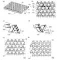
図1(a)は本実施例の2次元フォトニック結晶10の斜視図である。スラブ状の本体11の一方の表面には、円形の空孔12が周期的に形成されている。裏面も同様であるが、両者における空孔12の位置は相補的となっている。図1(b)に、本体11の第1表面131(図1(a)の上側の表面)及び第2表面132(下側の表面)における空孔12の配置を重ねて描いた図を示す。空孔12は、第1表面131では三角格子141の格子点121に配置されており、第2表面132では第1表面131の三角格子141に対して相補的な位置にある三角格子142の格子点122に配置されている。図1(b)及び(c)に太矢印で示すように、第1表面131の各格子点121から、第2表面132の格子点のうち最隣接の3個の格子点に向けて、それぞれ空孔柱12Aが延びている。同様に、図1(b)及び(d)に太矢印で示すように、第2表面132の各格子点122からは、第1表面131の格子点のうち最隣接の3個の格子点に向けてそれぞれ空孔柱12Aが延びている。
各空孔柱12Aは、本体11の厚さ方向のいずれの位置においても、面内断面の形状が同じ径を持つ円形になるように形成されている。すなわち、各空孔柱12Aは斜円柱状となっている。但し、図1(e)及び(f)に示すように、本体11内において、複数の空孔柱12Aは互いに重なり合い、その重なり合う領域の形状は本体の厚さ方向に変化してゆく。Examples of the two-dimensional photonic crystal according to the present invention will be described with reference to FIGS.
FIG. 1A is a perspective view of the two-
Each
本体内において空孔柱12Aがこのように形成されていることにより、面内断面では3個の空孔12を周期構造の単位16とする三角格子が形成される。第2表面132よりも第1表面131に近い面内断面151では、周期構造単位16は正三角形の3個の頂点に円形の空孔12を配置した形状を有し、三角格子141と同じ格子点上に配置されている(図1(e))。一方、第1表面131よりも第2表面132に近い面内断面152では、周期構造単位16は面内断面151のものを面に垂直な軸を中心に180°回転させた正三角形の3個の頂点に円形の空孔12を配置した形状を有し、三角格子142と同じ格子点上に配置されている(図1(f))。 By forming the
周期構造単位16の面内断面形状は、図2(a)に示すように、回転軸17のまわりに3回回転対称性を有する。なお、この面内断面形状は併せて、回転対称軸17を含む垂直鏡映対称面181、182及び183を持つ。即ち、この周期構造単位16の面内断面形状は特許文献2及び3に記載の2次元フォトニック結晶の空孔と同様にC3vの対称性を有する。空孔の半径が三角格子の周期の1/4以下である場合には、厚さ方向の中心付近では3個の空孔12は分離する(図2(b))。これら3個の空孔12相互間の距離は他の空孔との距離よりも小さいため、これら3個の空孔も1個の周期構造単位16として作用する。この場合にも周期構造単位16の面内断面での形状は3回回転対称性を含むC3vの対称性を有する。The in-plane cross-sectional shape of the periodic
本実施例の2次元フォトニック結晶10では、三角格子141及び142の格子定数aと本体11の厚さdの比により、空孔柱12Aの角度θが異なる。例えば、格子定数aを一定にすると、厚さdを小さくするほど角度θは大きくなる。従って、本体11内において空孔柱12Aにより形成される屈折率の周期分布は、格子定数a及び厚さdにより調整することができる。 In the two-
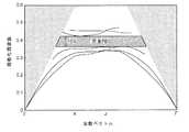
図3に、本実施例の2次元フォトニック結晶10について3次元時間領域差分法によりフォトニックバンドを計算した結果をグラフで示す。ここでは、半径rを格子定数aで除したr/a値が0.32、厚さtを格子定数aで除したt/a値が0.8である場合について計算した。この場合、角度θは36°となる。このグラフの横軸には波数ベクトルを、縦軸には周波数にa/c(cは光速)を乗じて無次元とした規格化周波数を、それぞれ用いた。グラフ中の曲線はフォトニックバンドを示す。本実施例では本体内部で空孔集合部の形状が厚さ方向の位置により異なることにより、明確にはTE偏波とTM偏波の2つの偏波に分離しない。そのため、この図では偏波に関わらず全てのフォトニックバンドについて表した。この計算結果により、規格化周波数が約0.4の中央値を持ち、その中央値に対して約15%の幅を持つ領域において完全PBG(図3の斜線部)が形成されていることが明らかになった。 In FIG. 3, the result of having calculated the photonic band by the three-dimensional time domain difference method about the two-
図4(a)に、r/a値が0.32及び0.25である場合についてそれぞれ、t/a値が0.4〜1.2の範囲内における完全PBGの幅を計算した結果を示す。図4(b)は、(a)のグラフと同じデータを、横軸を本体表面に対する法線と空孔柱の成す角度θで表したものである。r/a値が0.32である場合には、t/a値が0.6〜1.0の時に、前述のように光通信デバイスにおいて望ましいとされる10%以上の幅を持つ完全PBGが得られる。t/a値が0.4及び1.2である時には、特許文献2及び3に記載の2次元フォトニック結晶において得られていた完全PBG幅の最大値である4.4%よりも広い幅を持つ完全PBGが得られる。r/a値が0.25である場合には、t/a値が0.6〜0.8の時に特許文献2及び3に記載の2次元フォトニック結晶における完全PBGよりも広い約8%の幅を持つ完全PBGが得られる。 FIG. 4 (a) shows the result of calculating the width of the complete PBG when the r / a value is 0.32 and 0.25, and the t / a value is in the range of 0.4 to 1.2, respectively. FIG. 4B shows the same data as the graph of FIG. 4A, in which the horizontal axis represents the angle θ between the normal to the surface of the main body and the hole column. When the r / a value is 0.32, when the t / a value is 0.6 to 1.0, a complete PBG having a width of 10% or more desirable in an optical communication device as described above is obtained. When the t / a value is 0.4 and 1.2, a complete PBG having a width wider than 4.4% which is the maximum value of the complete PBG width obtained in the two-dimensional photonic crystal described in
次に、本発明の2次元フォトニック結晶の他の実施例を説明する。なお、ここでは、2次元フォトニック結晶10の構成要素と同じものにはそれと同じ符号を付し、詳細な説明を省略した。
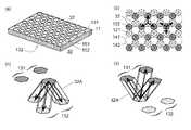
まず、3回回転対称性を持つ異屈折率領域を有する2次元フォトニック結晶の例として、正三角形の空孔22が三角格子状に配置された2次元フォトニック結晶20を、図5及び図6を用いて説明する。
図5(a)は2次元フォトニック結晶20の斜視図である。本体11の第1表面131には、正三角形の空孔22が三角格子の格子点121上に、その正三角形の各辺が格子と略平行になるように配置され、第2表面132には空孔22が第1表面131と相補的な位置に第1表面131と同じ向きで配置されている(図5(b))。
第1表面131の各格子点121から、第2表面132の格子点のうち最隣接の3個の格子点に向けて、それぞれ空孔柱22Aが延び(図5(b), (c))、同様に、第2表面132の各格子点122から、第1表面131の格子点のうち最隣接の3個の格子点に向けてそれぞれ空孔柱22Aが延びている(図5(b), (d))。
面内断面では3個の空孔22を周期構造の単位26とする三角格子が形成される。図5(e)及び(f)に面内断面151及び152における周期構造単位26の配置を、図6にそれら面内断面における周期構造単位26の拡大図を示す。図6には、図5(b)〜(d)に示した太矢印と同じ方向を示す太矢印を付した。面内断面151では、周期構造単位26の形状は3個の正三角形が重なった1個の正三角形になる。一方、面内断面152では、周期構造単位26は3個の正三角形がそれぞれ異なる1辺に垂直な方向にずれて重なった形状を有する。これら周期構造単位26はいずれもC3vの対称性を満たす。このような対称性を有することにより、この2次元フォトニック結晶20では完全PBGが形成される。Next, another embodiment of the two-dimensional photonic crystal of the present invention will be described. Here, the same components as those of the two-
First, as an example of a two-dimensional photonic crystal having a three-fold rotational symmetry, a two-
FIG. 5A is a perspective view of the two-
The
In the in-plane cross section, a triangular lattice having three
2次元フォトニック結晶20では空孔22の各辺は格子に平行になるように配置したが、図7(a)に示すように、空孔22の各辺が格子に対して同じ角度αだけ傾いて配置されている場合には、周期構造単位は、C3vの対称性は持たないが3回回転対称性を持つ(図7(b))。そのため、このような空孔を有する2次元フォトニック結晶にも完全PBGが形成される。In the two-
図8に、6回回転対称性を持つ異屈折率領域を有する2次元フォトニック結晶の例として、正六角形の空孔32が三角格子状に配置された2次元フォトニック結晶30を示す。図8(a)は2次元フォトニック結晶30の斜視図である。本体11の第1表面131には、正六角形の空孔32が三角格子の格子点121上に配置され、第2表面132には空孔32が第1表面131と相補的な位置に第1表面131と同じ向きで配置されている(図8(b))。空孔32の正六角形は、6本の辺が三角格子に直交するように配置されている。第1表面131の各格子点121及び第2表面132の各格子点122から、2次元フォトニック結晶10及び20と同様に空孔柱32Aが延びている(図8(c), (d))。
2次元フォトニック結晶30の面内断面151及び152における周期構造単位36は、2次元フォトニック結晶10及び20と同様に三角格子状に配置される。図9に、周期構造単位36の面内断面での形状を示す。この面内断面は、3個の正六角形が120°ずつ異なる方向にずれて重なった形状を有し、C3vの対称性を満たす。このような対称性を有することにより、この2次元フォトニック結晶30では完全PBGが形成される。FIG. 8 shows a two-
The periodic
正六角形の空孔32は、6本の辺を三角格子に直交するように配置する代わりに、図10に示すように、6本の辺を三角格子に平行に配置してもよい。この場合にも、周期構造単位36の面内断面はC3vの対称性を満たす。また、正六角形の各辺が格子に対して同じ角度(0°及び90°を除く)だけ傾くように空孔が配置されている場合には、周期構造単位は、C6vの対称性は持たないが6回回転対称性を持つため、完全PBGが形成される。The regular
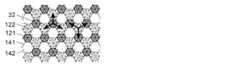
図11に、本実施例の2次元フォトニック結晶10を用いた光合分波器40の一例を示す。この光合分波器40は、1列分の格子点121の各々においてそこから延びる3個の空孔12を欠損させる(設けない)ことにより線状の欠陥を設け、その線状欠陥から3列離れた所にある1個の格子点121から延びる3個の空孔12を欠損させることにより点状の欠陥を設けたものである。この線状欠陥が導波路41となり、この点状欠陥が共振器42となる。 FIG. 11 shows an example of an optical multiplexer /
導波路41及び共振器42においては、完全PBG中に欠陥準位が形成される。それにより、導波路41では完全PBG中の特定の波長帯内にある波長の光が伝播することができる。また、共振器42は完全PBG中の特定の波長の光に共振する。導波路41の近傍に共振器42を設けることにより、光合分波器40は導波路41中を伝播する光のうち共振器42の共振波長を有する光を、共振器42を介して外部に取り出す分波器として機能する。それと共に、この共振波長を有する光を外部から共振器42を介して導波路41に導入する合波器としても機能する。 In the
線状欠陥や点状欠陥の形状を調整することにより、導波路の通過波長帯及び共振器の共振波長を制御することができる。例えば、上述の導波路41及び共振器42では、1個の格子点121から延びる3本の空孔柱12Aを全て欠損させたが、その代わりに1個又は2本の空孔柱12Aのみを欠損させた場合には通過波長帯及び共振波長は導波路41及び共振器42とは異なる値になる。また、空孔柱12Aを欠損させる代わりに他の空孔とは異なる径を有する空孔柱を設けること、あるいは一部の格子点121及び/又は122の位置を三角格子の格子点からずらすこと、等により導波路及び共振器を形成することもできる。
このようにして形成される、共振波長が異なる複数の共振器を導波路の近傍に配置することにより、各共振器がそれぞれ異なる波長の光を分波及び合波する光合分波器を得ることができる。By adjusting the shape of the line defect or the point defect, the pass wavelength band of the waveguide and the resonance wavelength of the resonator can be controlled. For example, in the above-described
By arranging a plurality of resonators having different resonance wavelengths formed in the vicinity of the waveguide, an optical multiplexer / demultiplexer in which each resonator demultiplexes and multiplexes light of different wavelengths is obtained. Can do.
10…2次元フォトニック結晶
11…本体
12、22、32…空孔
12A、22A、32A…空孔柱
121…三角格子141の格子点
122…三角格子142の格子点
131…第1表面
132…第2表面
141…第1表面131上の三角格子
142…第2表面132上の三角格子
151…第2表面132よりも第1表面131に近い面内断面
151…第1表面131よりも第2表面132に近い面内断面
16、26、36…周期構造単位
17…回転対称軸
181、182、183…垂直鏡映対称面
40…光合分波器
41…導波路
42…共振器DESCRIPTION OF
Claims (7)
Translated fromJapanese前記本体の一方の表面である第1表面において、異屈折率領域が三角格子状に、且つ各格子点に関して少なくとも3回回転対称性を持つように配置されており、
前記本体の他方の表面である第2表面において、異屈折率領域が前記第1表面の三角格子に対して相補的な位置にある三角格子状に、且つ各格子点に関して少なくとも3回回転対称性を持つように配置されており、
前記第1表面の各格子点から該格子点に最隣接である前記第2表面の3個の格子点に向けてそれぞれ異屈折率領域の柱が延びている、
ことを特徴とする2次元フォトニック結晶。A two-dimensional photonic crystal comprising a slab-shaped main body and periodically arranging regions having different refractive indices from the main body,
On the first surface, which is one surface of the main body, the different refractive index regions are arranged in a triangular lattice shape and at least three-fold rotational symmetry with respect to each lattice point,
In the second surface, which is the other surface of the main body, the refractive index region is in a triangular lattice shape in a position complementary to the triangular lattice of the first surface, and at least three times rotational symmetry with respect to each lattice point Are arranged to have
Columns of different refractive index regions extend from the respective lattice points on the first surface toward the three lattice points on the second surface that are nearest to the lattice point.
A two-dimensional photonic crystal characterized by that.
Priority Applications (7)
| Application Number | Priority Date | Filing Date | Title |
|---|---|---|---|
| JP2006077600AJP4900572B2 (en) | 2006-03-20 | 2006-03-20 | 2D photonic crystal |
| DE112007000664.1TDE112007000664B4 (en) | 2006-03-20 | 2007-03-20 | Two-dimensional photonic crystal, optical resonator device and optical multiplexer / demultiplexer |
| CN2007800099072ACN101405634B (en) | 2006-03-20 | 2007-03-20 | Two-dimensional photonic crystal |
| US12/225,185US8358895B2 (en) | 2006-03-20 | 2007-03-20 | Two-dimensional photonic crystal |
| KR1020087025519AKR101332293B1 (en) | 2006-03-20 | 2007-03-20 | Two-dimensional photonic crystal |
| PCT/JP2007/000269WO2007108219A1 (en) | 2006-03-20 | 2007-03-20 | Two-dimensional photonic crystal |
| TW096109455ATWI437296B (en) | 2006-03-20 | 2007-03-20 | Two - dimensional photon crystallization |
Applications Claiming Priority (1)
| Application Number | Priority Date | Filing Date | Title |
|---|---|---|---|
| JP2006077600AJP4900572B2 (en) | 2006-03-20 | 2006-03-20 | 2D photonic crystal |
Publications (2)
| Publication Number | Publication Date |
|---|---|
| JP2007256382A JP2007256382A (en) | 2007-10-04 |
| JP4900572B2true JP4900572B2 (en) | 2012-03-21 |
Family
ID=38522255
Family Applications (1)
| Application Number | Title | Priority Date | Filing Date |
|---|---|---|---|
| JP2006077600AExpired - Fee RelatedJP4900572B2 (en) | 2006-03-20 | 2006-03-20 | 2D photonic crystal |
Country Status (7)
| Country | Link |
|---|---|
| US (1) | US8358895B2 (en) |
| JP (1) | JP4900572B2 (en) |
| KR (1) | KR101332293B1 (en) |
| CN (1) | CN101405634B (en) |
| DE (1) | DE112007000664B4 (en) |
| TW (1) | TWI437296B (en) |
| WO (1) | WO2007108219A1 (en) |
Families Citing this family (10)
| Publication number | Priority date | Publication date | Assignee | Title |
|---|---|---|---|---|
| US8986558B2 (en) | 2008-09-01 | 2015-03-24 | Japan Science And Technology Agency | Plasma etching method, plasma etching device, and method for producing photonic crystal |
| US8923661B2 (en)* | 2011-07-27 | 2014-12-30 | Massachusetts Institute Of Technology | 2-pattern compound photonic crystals with a large, complete photonic band gap |
| CN102965728A (en)* | 2012-12-10 | 2013-03-13 | 常州大学 | Method for preparing single-layer two-dimensional photonic crystals by using cant-assisted gravity settling method |
| JP5900615B2 (en)* | 2013-04-12 | 2016-04-06 | 日本精工株式会社 | Target substance capture device |
| JP6281869B2 (en)* | 2014-02-27 | 2018-02-21 | 国立大学法人大阪大学 | Directional coupler and multiplexer / demultiplexer devices |
| CN103901536B (en)* | 2014-04-11 | 2016-08-17 | 深圳大学 | A kind of annulus bar and the Two dimensional square lattice photonic crystal of flat board connecting rod |
| CN108701965B (en)* | 2016-02-29 | 2020-08-25 | 国立大学法人京都大学 | Two-dimensional photonic crystal surface emitting laser and manufacturing method thereof |
| CN105891949B (en)* | 2016-05-20 | 2019-03-29 | 上海大学 | Preparation method based on laser ablation air column 2 D photon crystal |
| GB201903708D0 (en)* | 2019-03-19 | 2019-05-01 | Wave Optics Ltd | Improved angular uniformity waveguide for augmented or virtual reality |
| CN113419303B (en)* | 2021-06-11 | 2022-06-14 | 太原理工大学 | A two-dimensional hexagonal boron nitride valley photonic crystal unidirectional light transmission structure |
Family Cites Families (11)
| Publication number | Priority date | Publication date | Assignee | Title |
|---|---|---|---|---|
| WO1996029621A1 (en) | 1995-03-17 | 1996-09-26 | Massachusetts Institute Of Technology | Metallodielectric photonic crystal |
| JP3925769B2 (en) | 2000-03-24 | 2007-06-06 | 関西ティー・エル・オー株式会社 | Two-dimensional photonic crystal and multiplexer / demultiplexer |
| CN1184753C (en)* | 2001-08-08 | 2005-01-12 | 中国科学院物理研究所 | Photonic crystal wavelength division multiplexing device |
| JP3459827B2 (en)* | 2002-03-26 | 2003-10-27 | 科学技術振興事業団 | Two-dimensional photonic crystal optical multiplexer / demultiplexer |
| JP2004012780A (en)* | 2002-06-06 | 2004-01-15 | Seiko Epson Corp | Optical multiplexer / demultiplexer, optical communication device, and optical communication system |
| JP2004093787A (en)* | 2002-08-30 | 2004-03-25 | Seiko Epson Corp | Optical switch, optical communication device, and optical communication system |
| JP4247404B2 (en)* | 2003-02-27 | 2009-04-02 | 独立行政法人科学技術振興機構 | Photonic crystal and manufacturing method thereof |
| WO2004086102A1 (en)* | 2003-03-26 | 2004-10-07 | Tdk Corporation | Two-dimensional photonic crystal, and waveguide and resonator using the same |
| JP4538718B2 (en)* | 2003-08-28 | 2010-09-08 | アルプス電気株式会社 | Two-dimensional photonic crystal slab and two-dimensional photonic crystal waveguide |
| DE602005016330D1 (en)* | 2004-03-30 | 2009-10-15 | Canon Kk | Display device, image viewer, and projection device using the same |
| JP4297358B2 (en)* | 2004-08-30 | 2009-07-15 | 国立大学法人京都大学 | Two-dimensional photonic crystal and optical device using the same |
- 2006
- 2006-03-20JPJP2006077600Apatent/JP4900572B2/ennot_activeExpired - Fee Related
- 2007
- 2007-03-20USUS12/225,185patent/US8358895B2/ennot_activeExpired - Fee Related
- 2007-03-20WOPCT/JP2007/000269patent/WO2007108219A1/enactiveApplication Filing
- 2007-03-20TWTW096109455Apatent/TWI437296B/ennot_activeIP Right Cessation
- 2007-03-20CNCN2007800099072Apatent/CN101405634B/ennot_activeExpired - Fee Related
- 2007-03-20DEDE112007000664.1Tpatent/DE112007000664B4/ennot_activeExpired - Fee Related
- 2007-03-20KRKR1020087025519Apatent/KR101332293B1/ennot_activeExpired - Fee Related
Also Published As
| Publication number | Publication date |
|---|---|
| KR20090006101A (en) | 2009-01-14 |
| CN101405634A (en) | 2009-04-08 |
| JP2007256382A (en) | 2007-10-04 |
| CN101405634B (en) | 2010-07-21 |
| TWI437296B (en) | 2014-05-11 |
| US20090263094A1 (en) | 2009-10-22 |
| KR101332293B1 (en) | 2013-11-22 |
| TW200745647A (en) | 2007-12-16 |
| DE112007000664T5 (en) | 2009-02-12 |
| US8358895B2 (en) | 2013-01-22 |
| DE112007000664B4 (en) | 2019-03-07 |
| WO2007108219A1 (en) | 2007-09-27 |
Similar Documents
| Publication | Publication Date | Title |
|---|---|---|
| JP4900572B2 (en) | 2D photonic crystal | |
| JP4923234B2 (en) | Two-dimensional photonic crystal and optical device using the same | |
| JP3721181B2 (en) | Electromagnetic frequency filter | |
| JP5272173B2 (en) | 2D photonic crystal | |
| US6597851B2 (en) | Periodic dielectric structure having a complete three-dimensional photonic band gap | |
| JP4297358B2 (en) | Two-dimensional photonic crystal and optical device using the same | |
| JP3459827B2 (en) | Two-dimensional photonic crystal optical multiplexer / demultiplexer | |
| JP4025738B2 (en) | 2D photonic crystal | |
| US7509013B2 (en) | Two-dimensional photonic crystal | |
| JP4669923B2 (en) | Polarization mode converter | |
| EP1569017A1 (en) | Two-dimensional photonic crystal optical multiplexer/demultiplexer utilizing boundary rflection | |
| JP4538718B2 (en) | Two-dimensional photonic crystal slab and two-dimensional photonic crystal waveguide | |
| JP3999152B2 (en) | Two-dimensional photonic crystal slab and optical device using the same | |
| JP6530332B2 (en) | Optical waveguide and drop filter | |
| US6993234B1 (en) | Photonic crystal resonator apparatus with improved out of plane coupling | |
| Gulzari et al. | Vibration Resonance and Dynamic Characteristics of Pillared Phononic Crystals and Acoustic | |
| WO2003023470A1 (en) | Large-bandwidth photonic crystal waveguides | |
| JP2006178209A (en) | Waveguide | |
| Chen et al. | The disorder effect on the performance of novel waveguides constructed in two-dimensional amorphous photonic materials |
Legal Events
| Date | Code | Title | Description |
|---|---|---|---|
| A621 | Written request for application examination | Free format text:JAPANESE INTERMEDIATE CODE: A621 Effective date:20080828 | |
| TRDD | Decision of grant or rejection written | ||
| A01 | Written decision to grant a patent or to grant a registration (utility model) | Free format text:JAPANESE INTERMEDIATE CODE: A01 Effective date:20111129 | |
| A01 | Written decision to grant a patent or to grant a registration (utility model) | Free format text:JAPANESE INTERMEDIATE CODE: A01 | |
| A61 | First payment of annual fees (during grant procedure) | Free format text:JAPANESE INTERMEDIATE CODE: A61 Effective date:20111220 | |
| R150 | Certificate of patent or registration of utility model | Ref document number:4900572 Country of ref document:JP Free format text:JAPANESE INTERMEDIATE CODE: R150 Free format text:JAPANESE INTERMEDIATE CODE: R150 | |
| FPAY | Renewal fee payment (event date is renewal date of database) | Free format text:PAYMENT UNTIL: 20150113 Year of fee payment:3 | |
| R250 | Receipt of annual fees | Free format text:JAPANESE INTERMEDIATE CODE: R250 | |
| S111 | Request for change of ownership or part of ownership | Free format text:JAPANESE INTERMEDIATE CODE: R313117 | |
| R350 | Written notification of registration of transfer | Free format text:JAPANESE INTERMEDIATE CODE: R350 | |
| R250 | Receipt of annual fees | Free format text:JAPANESE INTERMEDIATE CODE: R250 | |
| R250 | Receipt of annual fees | Free format text:JAPANESE INTERMEDIATE CODE: R250 | |
| R250 | Receipt of annual fees | Free format text:JAPANESE INTERMEDIATE CODE: R250 | |
| R250 | Receipt of annual fees | Free format text:JAPANESE INTERMEDIATE CODE: R250 | |
| S111 | Request for change of ownership or part of ownership | Free format text:JAPANESE INTERMEDIATE CODE: R313117 | |
| R350 | Written notification of registration of transfer | Free format text:JAPANESE INTERMEDIATE CODE: R350 | |
| S111 | Request for change of ownership or part of ownership | Free format text:JAPANESE INTERMEDIATE CODE: R313113 | |
| R350 | Written notification of registration of transfer | Free format text:JAPANESE INTERMEDIATE CODE: R350 | |
| R250 | Receipt of annual fees | Free format text:JAPANESE INTERMEDIATE CODE: R250 | |
| R250 | Receipt of annual fees | Free format text:JAPANESE INTERMEDIATE CODE: R250 | |
| R250 | Receipt of annual fees | Free format text:JAPANESE INTERMEDIATE CODE: R250 | |
| LAPS | Cancellation because of no payment of annual fees |