JP4898598B2 - Cooling structure of rack mount type control device and rack type storage control device - Google Patents
Cooling structure of rack mount type control device and rack type storage control deviceDownload PDFInfo
- Publication number
- JP4898598B2 JP4898598B2JP2007220647AJP2007220647AJP4898598B2JP 4898598 B2JP4898598 B2JP 4898598B2JP 2007220647 AJP2007220647 AJP 2007220647AJP 2007220647 AJP2007220647 AJP 2007220647AJP 4898598 B2JP4898598 B2JP 4898598B2
- Authority
- JP
- Japan
- Prior art keywords
- cooling
- control board
- power supply
- passage
- housing
- Prior art date
- Legal status (The legal status is an assumption and is not a legal conclusion. Google has not performed a legal analysis and makes no representation as to the accuracy of the status listed.)
- Expired - Fee Related
Links
Images


Classifications
- G—PHYSICS
- G11—INFORMATION STORAGE
- G11B—INFORMATION STORAGE BASED ON RELATIVE MOVEMENT BETWEEN RECORD CARRIER AND TRANSDUCER
- G11B33/00—Constructional parts, details or accessories not provided for in the other groups of this subclass
- G11B33/14—Reducing influence of physical parameters, e.g. temperature change, moisture, dust
- G11B33/1406—Reducing the influence of the temperature
- G11B33/1413—Reducing the influence of the temperature by fluid cooling
- G11B33/142—Reducing the influence of the temperature by fluid cooling by air cooling
- H—ELECTRICITY
- H05—ELECTRIC TECHNIQUES NOT OTHERWISE PROVIDED FOR
- H05K—PRINTED CIRCUITS; CASINGS OR CONSTRUCTIONAL DETAILS OF ELECTRIC APPARATUS; MANUFACTURE OF ASSEMBLAGES OF ELECTRICAL COMPONENTS
- H05K7/00—Constructional details common to different types of electric apparatus
- H05K7/20—Modifications to facilitate cooling, ventilating, or heating
- H05K7/20709—Modifications to facilitate cooling, ventilating, or heating for server racks or cabinets; for data centers, e.g. 19-inch computer racks
- H05K7/20718—Forced ventilation of a gaseous coolant
- H05K7/20727—Forced ventilation of a gaseous coolant within server blades for removing heat from heat source
Landscapes
- Engineering & Computer Science (AREA)
- Computer Hardware Design (AREA)
- General Engineering & Computer Science (AREA)
- Physics & Mathematics (AREA)
- Thermal Sciences (AREA)
- Microelectronics & Electronic Packaging (AREA)
- Cooling Or The Like Of Electrical Apparatus (AREA)
- Secondary Cells (AREA)
Description
Translated fromJapanese本発明は、ラックマウント型制御装置の冷却構造及びラック型記憶制御装置に関するものである。 The present invention relates to a cooling structure for a rack mount type control device and a rack type storage control device.
記憶制御装置は、多数のディスクドライブをアレイ状に接続した記憶部を備えており、サーバ等のホストコンピュータ(以下「ホスト」)に、論理的な記憶領域(論理ボリューム)を提供する。信頼性等を高めるために、記憶制御装置では、RAID(Redundant Array of Independent Disks)に基づく冗長化された記憶領域をホストに提供する。 The storage control device includes a storage unit in which a large number of disk drives are connected in an array, and provides a logical storage area (logical volume) to a host computer such as a server (hereinafter “host”). In order to improve reliability and the like, the storage control device provides a redundant storage area based on RAID (Redundant Array of Independent Disks) to the host.
記憶制御装置の筐体内に収容されるコントローラや多数のディスクドライブ及び電源関連装置は、それぞれ熱を発生するため、これらコントローラや各ディスクドライブ及び電源関連装置をそれぞれ冷却する必要がある。大型の冷却ファン装置によって筐体内を空冷する場合、冷却対象の各部(コントローラ、ディスクドライブ、電源関連装置である)を均一に冷却するのは難しい。冷却対象の各部を十分冷却するためには、より強力な冷却ファンを設ける必要があり、製造コストや電気料金が増大する。 Since the controller and a large number of disk drives and power supply-related devices housed in the storage control device casing each generate heat, it is necessary to cool these controllers, disk drives, and power supply-related devices. When the inside of a housing is air-cooled by a large cooling fan device, it is difficult to uniformly cool each part to be cooled (controller, disk drive, power supply related device). In order to sufficiently cool each part to be cooled, it is necessary to provide a more powerful cooling fan, which increases manufacturing costs and electricity charges.
そこで、記憶制御装置をNAS(Network Attached Storage)ヘッド搭載領域、論理基板搭載領域及び電源搭載領域の複数の領域に分割し、各領域毎に個別の冷却機構をそれぞれ設けて冷却するようにした記憶制御装置も提案されている(特許文献1)。
前記文献に記載の従来技術は、いわゆる大型の記憶制御装置に関するもので、ラック型の記憶制御装置にそのまま適用することはできない。大型の記憶制御装置では、筐体の中央で下から上に冷却風を流通させるための冷却通路を備えるが、ラック型記憶制御装置は、そのような中央冷却通路を備えない。 The prior art described in the above document relates to a so-called large storage control device and cannot be applied to a rack type storage control device as it is. A large storage control device includes a cooling passage for circulating cooling air from the bottom to the top in the center of the housing, but the rack-type storage control device does not include such a central cooling passage.
また、上記文献に記載の従来技術では、中央冷却通路に冷却風を導くために、接続用基板に冷却穴を設ける必要がある。従って、接続用基板の全面積のうち電気的接続に使用可能な面積が低下するため、より多くの基板や装置を高密度に実装するのが難しい。 Moreover, in the prior art described in the above document, it is necessary to provide a cooling hole in the connection substrate in order to guide the cooling air to the central cooling passage. Therefore, since the area that can be used for electrical connection is reduced in the total area of the connection substrate, it is difficult to mount more substrates and devices at high density.
そこで、本発明の目的は、冷却効率を改善できるようにしたラックマウント型制御装置の冷却構造及びラック型記憶制御装置を提供することにある。本発明の他の目的は、接続用基板の前後にそれぞれ制御基板群及び電源関連装置が高密度で実装された筐体内を効率的に冷却することができるようにしたラックマウント型制御装置の冷却構造及びラック型記憶制御装置を提供することにある。本発明のさらなる目的は、後述する実施形態の記載から明らかになるであろう。 SUMMARY OF THE INVENTION Accordingly, an object of the present invention is to provide a cooling structure for a rack mount type control device and a rack type storage control device which can improve the cooling efficiency. Another object of the present invention is to cool a rack-mounted control device that can efficiently cool the inside of a housing in which control board groups and power-related devices are mounted at high density before and after the connection board. The object is to provide a structure and a rack-type storage control device. The further objective of this invention will become clear from description of embodiment mentioned later.
上記課題を解決すべく、本発明の一つの観点に従う、ラックマウント型の制御装置の冷却構造は、前面及び後面がそれぞれ開口する筐体と、筐体の内部を前後に分割するようにして筐体の中央部に設けられる接続用基板と、筐体の前面側及び後面側にそれぞれ設けられ、記憶デバイスに関する制御を実行するための複数の制御基板を含む制御基板群と、各制御基板群の左右両側にそれぞれ設けられる電源関連装置と、各制御基板群を第1冷却風によってそれぞれ冷却する第1冷却通路と、各電源関連装置のうち各制御基板群の一側に位置する電源関連装置を第2冷却風によってそれぞれ冷却する第2冷却通路と、各電源関連装置のうち各制御基板群の他側に位置する電源関連装置を第3冷却風によってそれぞれ冷却するための第3冷却通路と、を備え、第1、第2、第3冷却通路の上流側は互いに独立して設けられており、かつ、第1、第2、第3冷却通路の下流側は共通している。 In order to solve the above problems, according to one aspect of the present invention, a cooling structure for a rack-mount type control device includes a housing having front and rear openings, and a housing that is divided into front and rear portions. A connection board provided at the center of the body, a control board group including a plurality of control boards provided on the front side and the rear side of the housing, respectively, for executing control related to the storage device, and A power-related device provided on each of the left and right sides, a first cooling passage for cooling each control board group with a first cooling air, and a power-related device located on one side of each control board group among the power-related devices. A second cooling passage for cooling by the second cooling air, and a third cooling passage for cooling the power-related devices located on the other side of each control board group by the third cooling air, respectively. Comprising a first, second, upstream side of the third cooling passage is provided independently of each other, and first, second, downstream of the third cooling passage are common.
本発明の実施形態では、第1冷却通路の流入口には吸い込みファンが、第1冷却通路の流出口には吸い出しファンがそれぞれ設けられている。 In the embodiment of the present invention, a suction fan is provided at the inlet of the first cooling passage, and a suction fan is provided at the outlet of the first cooling passage.
本発明の実施形態では、吸い込みファンは、各制御基板群のうち筐体の前面側に位置する前側制御基板群の上側に設けられており、吸い出しファンは、各制御基板群のうち筐体の後面側に位置する後側制御基板群の上側に設けられている。 In the embodiment of the present invention, the suction fan is provided on the upper side of the front control board group located on the front side of the casing among the control board groups, and the suction fan is provided on the casing of the control board group. It is provided on the upper side of the rear control board group located on the rear surface side.
本発明の実施形態では、第1冷却通路は、吸い込みファンの下流側に位置して前側制御基板群の上部に設けられる流入部と、この流入部に連通して設けられ、前側制御基板群を構成する各制御基板間に形成される前側流路部と、この前側流路部に連通して設けられ、筐体の前面側から後面側にわたって筐体の下側に形成される第1下部通路と、この第1下部通路に連通して設けられ、後側制御基板群を構成する各制御基板間に形成される後側流路部と、この後側流路部に連通して、吸い出しファンの上流側に位置して後側制御基板群の上部に設けられる流出部と、を備えて構成される。 In the embodiment of the present invention, the first cooling passage is provided on the downstream side of the suction fan and provided at the upper part of the front control board group, and is provided in communication with the inflow part. A front flow path portion formed between the control boards constituting the first flow path, and a first lower passage formed in communication with the front flow path portion and formed on the lower side of the casing from the front side to the rear side of the casing And a rear flow path portion provided between the control boards constituting the rear control board group, and a suction fan connected to the rear flow path section. And an outflow portion provided on the upper side of the rear control board group.
本発明の実施形態では、第2冷却通路及び第3冷却通路は、各電源関連装置のうち筐体の前面側に位置する前側電源関連装置内に設けられ、この前側電源関連装置の前面から流入する空気を下側に向けて流出させる前側流路部と、この前側流路部に連通して設けられ、筐体の前面側から後面側にわたって筐体の下側に形成される第2下部通路と、この第2下部通路に連通して、各電源関連装置のうち筐体の後面側に位置する後側電源関連装置内に設けられ、第2下部通路から流入する空気を上側に向けて流出させる後側流路部と、この後側流路部と第1冷却通路の流出部とを連通させるようにして、後側電源関連装置の上部に設けられる接続部と、を備えて構成される。 In the embodiment of the present invention, the second cooling passage and the third cooling passage are provided in a front power supply related device located on the front side of the housing among the power supply related devices, and flow from the front of the front power supply related device. And a second lower passage formed on the lower side of the casing from the front side to the rear side of the casing. The second lower passage communicates with the second lower passage and is provided in a rear power supply device located on the rear surface side of the housing among the power supply devices, and the air flowing in from the second lower passage flows upward. And a connecting portion provided on the upper part of the rear power supply related device so as to communicate the rear channel portion and the outflow portion of the first cooling passage. .
本発明の実施形態では、第1下部通路と第2下部通路とは、空気が流通しないように独立して設けられている。 In the embodiment of the present invention, the first lower passage and the second lower passage are provided independently so that air does not flow.
本発明の実施形態では、後側電源関連装置は、冷却ファンを内蔵している。 In the embodiment of the present invention, the rear power supply-related device has a built-in cooling fan.
本発明の実施形態では、前側電源関連装置はバッテリ装置であり、後側電源関連装置は電源供給装置である。 In the embodiment of the present invention, the front power-related device is a battery device, and the rear power-related device is a power supply device.
本発明の実施形態では、各制御基板群の上下両端に位置して、各制御基板群を構成する各制御基板を支持するための基板支持部が接続用基板に設けられており、この基板支持部には、各制御基板間に空気を流通させるための冷却穴が設けられている。 In the embodiment of the present invention, the substrate support portions for supporting each control board constituting each control board group are provided on the connection board, which are positioned at the upper and lower ends of each control board group. The part is provided with cooling holes for allowing air to flow between the control boards.
本発明の実施形態では、第1下部通路の下側と筐体の内面との間に、前側制御基板群を構成する各制御基板にケーブルを接続するためのケーブル通路が設けられている。 In the embodiment of the present invention, a cable passage for connecting a cable to each control board constituting the front control board group is provided between the lower side of the first lower passage and the inner surface of the housing.
本発明の実施形態では、前側電源関連装置は、前側制御基板群の左右両側にそれぞれ複数ずつ設けられており、かつ、後側電源関連装置は、後側制御基板の左右両側にそれぞれ複数ずつ設けられている。 In the embodiment of the present invention, a plurality of front power supply-related devices are provided on both the left and right sides of the front control board group, and a plurality of rear power supply related devices are provided on the left and right sides of the rear control board. It has been.
本発明の実施形態では、各前側電源関連装置は、前側制御基板群の左右両側に位置して、空気が流通可能なように上下2段に重ねて設けられており、各後側電源関連装置は、後側制御基板群の左右両側に位置して、空気が流通可能なように上下2段に重ねて設けられている。 In the embodiment of the present invention, each front-side power-related device is positioned on both the left and right sides of the front-side control board group, and is provided in two upper and lower layers so that air can flow. Are located on the left and right sides of the rear control board group, and are provided in two upper and lower layers so that air can flow.
本発明の実施形態では、各制御基板群及び各電源関連装置のうち筐体の左半分に属する各制御基板群及び各電源関連装置によって第1クラスタが構成され、各制御基板群及び各電源関連装置のうち筐体の右半分に属する各制御基板群及び各電源関連装置によって第2クラスタが構成される。 In the embodiment of the present invention, among each control board group and each power supply related device, each control board group and each power supply related device belonging to the left half of the casing constitutes a first cluster, and each control board group and each power supply related device. A second cluster is constituted by each control board group and each power supply related device belonging to the right half of the casing among the devices.
本発明の実施形態では、筐体の前側の上部または後側の上部のいずれか一方に、制御装置を管理するための管理装置が水平に設けられている。 In the embodiment of the present invention, a management device for managing the control device is horizontally provided on either the front upper portion or the rear upper portion of the housing.
本発明の実施形態では、各制御基板群及び各電源関連装置は、ラックと異なる構造の筐体にも、そのまま転用することができるように構成されている。 In the embodiment of the present invention, each control board group and each power supply related device are configured so that they can be used as they are for a housing having a structure different from that of the rack.
本発明の他の観点に従う、ラックと、このラックに着脱可能に設けられる複数の記憶デバイス格納装置と、ラックに着脱可能に設けられ、各記憶デバイス格納装置に収容される複数の記憶デバイスを制御するための一つの制御装置と、を備えるラック型記憶制御装置では、制御装置は、ラックに収容されるラックマウント型の筐体と、筐体の内部を前後に分割するようにして筐体の中央部に設けられる接続用基板と、筐体の前面側及び後面側にそれぞれ設けられる制御基板群であって、データ入出力を要求するコマンドを発行する装置との間の通信を担当する第1通信制御基板と、各記憶デバイスとの間の通信を担当する第2通信制御基板と、第1通信制御基板及び第2通信制御基板にメモリ領域をそれぞれ提供するメモリ制御基板とを含む制御基板群と、各制御基板群を上下両端からそれぞれ支持する基板支持部であって、各制御基板群を構成する制御基板間に空気を流通させる複数の冷却穴を有する基板支持部と、各制御基板群のうち筐体の前面側に位置する前側制御基板群の左右両側に上下2段に重ねてそれぞれ配置されるバッテリ装置と、各制御基板群のうち筐体の後面側に位置する後側制御基板群の左右両側に上下2段に重ねてそれぞれ配置される電源供給装置であって、冷却ファンを内蔵する電源供給装置と、前側制御基板群の上部に設けられる吸い込みファンと、後側制御基板群の上部に設けられる吸い出しファンと、各制御基板群を冷却するための第1冷却通路であって、吸い込みファンの下流側に位置して前側制御基板群の上部に設けられる流入部と、この流入部に連通して設けられ、基板支持部の各冷却穴と前側制御基板群を構成する各制御基板間の隙間とによって形成される前側流路部と、この前側流路部に連通して設けられ、筐体の前面側から後面側にわたって筐体の下側に形成される第1下部通路と、この第1下部通路に連通して設けられ、基板支持部の各冷却穴と後側制御基板群を構成する各制御基板間の隙間とによって形成される後側流路部と、この後側流路部に連通して、吸い出しファンの上流側に位置して後側制御基板群の上部に設けられる流出部と、を備える第1冷却通路と、筐体の左側に位置するバッテリ装置及び電源供給装置をそれぞれ冷却するための第2冷却通路であって、バッテリ装置の前面から流入する空気を下側に向けて流出させる前側流路部と、この前側流路部に連通して設けられ、筐体の前面側から後面側にわたって筐体の下側に形成される第2下部通路と、この第2下部通路に連通して、電源供給装置内に設けられ、第2下部通路から流入する空気を上側に向けて流出させる後側流路部と、この後側流路部と第1冷却通路の流出部とを連通させるようにして、電源供給装置の上部に設けられる接続部と、を備える第2冷却通路と、筐体の右側に位置するバッテリ装置及び電源供給装置をそれぞれ冷却するための第3冷却通路であって、バッテリ装置の前面から流入する空気を下側に向けて流出させる前側流路部と、この前側流路部に連通して設けられ、筐体の前面側から後面側にわたって筐体の下側に形成される第2下部通路と、この第2下部通路に連通して、電源供給装置内に設けられ、第2下部通路から流入する空気を上側に向けて流出させる後側流路部と、この後側流路部と第1冷却通路の流出部とを連通させるようにして、電源供給装置の上部に設けられる接続部と、を備える第3冷却通路と、第1下部通路の下側と筐体の内面との間に設けられ、前側制御基板群を構成する各制御基板にケーブルを接続するためのケーブル通路と、を備える。 According to another aspect of the present invention, a rack, a plurality of storage device storage devices detachably provided in the rack, and a plurality of storage devices detachably provided in the rack and accommodated in the storage device storage devices are controlled. In a rack-type storage control device comprising a single control device, the control device includes a rack-mountable housing housed in the rack and a housing in a manner that divides the interior of the housing into the front and rear. A connection board provided in the central portion and a control board group provided on each of the front side and the rear side of the housing, and is in charge of communication with a device that issues a command for requesting data input / output. A communication control board; a second communication control board in charge of communication with each storage device; and a memory control board that provides a memory area to each of the first communication control board and the second communication control board. A control board group, and a board support section for supporting each control board group from both upper and lower ends, each board support section having a plurality of cooling holes for circulating air between the control boards constituting each control board group; Among the control board groups, battery devices arranged in two upper and lower layers on the left and right sides of the front side control board group located on the front side of the chassis, and the rear of the control board groups located on the rear side of the chassis A power supply device arranged in two upper and lower layers on both the left and right sides of the side control board group, including a cooling fan, a suction fan provided at the top of the front control board group, and a rear side A suction fan provided in the upper part of the control board group, and a first cooling passage for cooling each control board group, and an inflow part provided in the upper part of the front control board group located downstream of the suction fan; This inflow A front channel portion formed by each cooling hole of the substrate support portion and a gap between the control substrates constituting the front control substrate group, and provided in communication with the front channel portion. A first lower passage formed on the lower side of the housing from the front surface side to the rear surface side of the housing, and each cooling hole of the substrate support portion and the rear control board group provided in communication with the first lower passage. The rear flow path portion formed by the gaps between the control boards constituting each of the control circuit boards and the rear flow path sections are provided on the upper side of the rear control board group, located upstream of the suction fan. And a second cooling passage for cooling the battery device and the power supply device located on the left side of the housing, respectively, and lowers the air flowing in from the front surface of the battery device. The front channel part that flows out toward the side and the front channel part communicate with the front channel part A second lower passage formed on the lower side of the casing from the front side to the rear side of the casing, and a second lower passage provided in the power supply device in communication with the second lower passage. A connection provided at the upper part of the power supply device in such a manner that the rear flow path section for allowing the air flowing in from the passage to flow upward and the rear flow path section and the outflow section of the first cooling path communicate with each other. And a third cooling passage for cooling the battery device and the power supply device located on the right side of the housing, respectively, wherein air flowing in from the front surface of the battery device is directed downward A front-side flow channel portion that flows out toward the front side, a second lower passage that is provided in communication with the front-side flow channel portion and is formed on the lower side of the housing from the front side to the rear surface side of the housing, and the second lower portion A second lower passage provided in the power supply device in communication with the passage; A rear flow path section for flowing out the air flowing in from the upper side, and a connection section provided at the upper part of the power supply device so as to communicate with the rear flow path section and the outflow section of the first cooling passage A third cooling passage, a cable passage for connecting a cable to each control board that is provided between the lower side of the first lower passage and the inner surface of the housing, and the front control board group, Is provided.
本発明の実施形態では、接続用基板は、少なくとも各制御基板群が接続される範囲内に、筐体の前後に空気を積極的に流通させるための冷却穴が設けられていない。 In the embodiment of the present invention, the connection board is not provided with a cooling hole for positively circulating air before and after the housing within at least a range to which each control board group is connected.
本発明の実施形態では、筐体の上部には、制御装置の状態に関する情報を各制御基板から収集して管理するための管理装置が、水平方向に載置されており、管理装置に冷却風を供給するための第4冷却通路が、第1、第2、第3冷却通路とは独立して、筐体の上部に設けられている。 In the embodiment of the present invention, a management device for collecting and managing information on the state of the control device from each control board is placed in the upper part of the housing in the horizontal direction. A fourth cooling passage for supplying is provided in the upper part of the housing independently of the first, second and third cooling passages.
本発明のさらに別の観点に従う、制御装置の冷却構造は、前面及び後面がそれぞれ開口する筐体と、筐体の内部を前後に分割するようにして筐体の中央部に設けられ、冷却穴を実質的に備えない接続用基板と、筐体の前面側及び後面側にそれぞれ設けられ、記憶デバイスに関する制御を実行するための複数の制御基板を含む制御基板群と、各制御基板群の左右両側にそれぞれ設けられる電源関連装置と、各制御基板群を第1冷却風によってそれぞれ冷却する第1冷却通路と、各電源関連装置のうち各制御基板群の一側に位置する電源関連装置を第2冷却風によってそれぞれ冷却する第2冷却通路と、各電源関連装置のうち各制御基板群の他側に位置する電源関連装置を第3冷却風によってそれぞれ冷却するための第3冷却通路と、を備え、第1、第2、第3冷却通路は、接続用基板を迂回するようにして屈曲して形成されている。 According to still another aspect of the present invention, a cooling structure for a control device includes a housing having front and rear surfaces opened respectively, and a cooling hole provided in a central portion of the housing so as to divide the interior of the housing into front and rear. A control board group including a plurality of control boards provided on the front side and the rear side of the housing, each of which is provided on the front side and the rear side of the housing, and left and right of each control board group A power-related device provided on each side, a first cooling passage for cooling each control board group with the first cooling air, and a power-related device located on one side of each control board group among the power-related devices A second cooling passage for cooling by each of the two cooling winds, and a third cooling passage for cooling each of the power-related devices by the third cooling air for the power-related devices located on the other side of each control board group. Prepared, second , Second, third cooling passages are formed by bending so as to bypass the connection substrate.
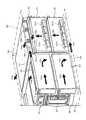
以下、図面に基づき、本発明の実施の形態を説明する。図1は、本実施形態の概要を示す説明図である。図1(a)には、ラック型の記憶制御装置に用いられるコントローラ1が示されている。このコントローラ1は、ラックマウント型のコントローラ1として構成され、ラックに取り付けられる。ラック型記憶制御装置の全体構成及びコントローラ1の詳細については、後述の実施例で詳細に説明する。 Hereinafter, embodiments of the present invention will be described with reference to the drawings. FIG. 1 is an explanatory diagram showing an outline of the present embodiment. FIG. 1A shows a
コントローラ1は、例えば、筐体2と、接続用基板3と、制御基板としての論理基板4と、バッテリ装置5と、冷却ファン6と、下部通路7A,7Bと、ケーブル通路7Cと、電源供給装置8と、サービスプロセッサ(以下、SVP)9とを備えている。 The
筐体2は、ラックマウント型の筐体として構成されており、4つの側面で囲まれた角筒状に形成されている。即ち、筐体2の前面及び後面はそれぞれ開口している。筐体2の中央部には、筐体2内部を前後に区切るようにして接続用基板3が設けられている。 The casing 2 is configured as a rack mount type casing, and is formed in a rectangular tube shape surrounded by four side surfaces. That is, the front surface and the rear surface of the housing 2 are opened. A
接続用基板3の前面及び後面には、それぞれ複数の論理基板4が着脱可能に取り付けられている。筐体2の前側に位置する複数の論理基板4を前側論理基板群と、筐体2の後側に位置する複数の論理基板4を後側論理基板群と、それぞれ呼ぶことができる。なお、図1(a)では、便宜上、コントローラ1の前側の構成を中心に示しており、コントローラ1の後側の構成は割愛されている。 A plurality of
論理基板4としては、例えば、ホストと通信するためのチャネルアダプタ基板、ディスクドライブと通信するためのディスクアダプタ基板、チャネルアダプタ基板及びディスクアダプタ基板に共有メモリ及びキャッシュメモリをそれぞれ提供するメモリ基板等を挙げることができる。接続用基板3には、各論理基板4と電気的に接続するためのコネクタや配線が設けられている。各論理基板4は、接続用基板3を介して、他の論理基板等と通信することができる。 Examples of the
接続用基板3には、冷却風を流通させるための冷却穴は設けられていない。後述のように、コントローラ1は、接続用基板3の下側を迂回して冷却風を流通させる複数の独立した冷却通路を備えている。 The
筐体2の前面には、論理基板4の左右両側に位置して、バッテリ装置5が上下2段に重ねて配置されている。筐体2の後面には、論理基板4の左右両側に位置して、電源供給装置8が上下2段に重ねて配置されている。 On the front surface of the housing 2,
筐体2の前面の論理基板4及び筐体2の後面の論理基板4の上側には、冷却ファン6がそれぞれ設けられている。前側の冷却ファン6は、吸い込みファンとして構成されており、筐体2の前面から空気を吸い込んで、吸い込んだ空気を筐体2内に排出する。後側の冷却ファン6は、吸い出しファンとして構成されており、筐体2内から空気を吸い込んで筐体2の後側に排出する。 Cooling
論理基板4の下側には、第1下部通路7Aが設けられている。論理基板4の左右両側に位置するバッテリ装置5及び電源供給装置8の下側には、第1下部通路から独立した第2下部通路7Bがそれぞれ設けられている。 A first lower passage 7 </ b> A is provided below the
第1下部通路7Aの下側には、ケーブル通路7Cが設けられている。前側の論理基板4の前面にはコネクタが設けられており、このコネクタにケーブルの一端が接続される。ケーブルの他端は、ケーブル通路7Cを介して筐体2の後側に引き出される。 A
SVP9は、後側の冷却ファン6の上側に位置して、筐体2内に水平に設けられる。SVP9は、コントローラ1内の各種状態に関する情報を収集し、図外の管理装置に提供するものである。 The
次に、コントローラ1内に設けられる複数の冷却通路について説明する。コントローラ1内は、複数の領域に分割されており、各領域毎にそれぞれ専用の冷却通路が設けられている。 Next, a plurality of cooling passages provided in the
図1(b)は、図1(a)中の矢示b−b線から見た状態を模式的に示す。図1(b)には、図1(a)の前面(正面)から見て左側に設けられる第2冷却通路の構成が示されている。 FIG.1 (b) shows typically the state seen from the arrow bb line | wire in Fig.1 (a). FIG. 1B shows the configuration of the second cooling passage provided on the left side when viewed from the front (front) of FIG.
第2冷却通路は、例えば、前側流路部と、第2下部通路7Bと、後側流路部と、接続部とを備えて構成される。前側流路部は、矢示FB1に示すように、バッテリ装置5の前面からバッテリ装置5内に流入した空気を、バッテリ装置5の下側に向けて流出させる。即ち、各バッテリ装置5の前面及び下面には、空気が流通するための複数の穴がそれぞれ設けられている。矢示FB1の冷却風により、各バッテリ装置5がそれぞれ冷却される。第2下部通路7Bは、矢示FB2に示すように、バッテリ装置5から流入した空気を水平方向に流通させ、筐体後方に位置する電源供給装置8の下側まで導く。 The second cooling passage includes, for example, a front channel portion, a second
各電源供給装置8内には、専用の冷却ファン8Aがそれぞれ設けられている。このファン8Aを装置内ファンと呼ぶこともできる。各ファン8A及び吸い出しファン6によって、第2冷却通路内に圧力差が生じ、外気をバッテリ装置5内に流入させ、第2下部通路7Bを介して電源供給装置8に送り込むことができる。 Each
第2下部通路7Bから電源供給装置8内に流入した空気は、矢示FB3に示すように、電源供給装置8内を冷却しながら上昇する。電源供給装置8を冷却した空気は、矢示FB4に示すように、電源供給装置8内から流出して、接続部に流入する。接続部とは、第2冷却通路の下流側を第1冷却通路の下流側に接続するための空間である。例えば、SVP9の下面と電源供給装置8の上面との間の空間が接続部として機能する。これにより、第2冷却通路の空気は、第1冷却通路の下流に流入し、筐体2の後方に位置する吸い出しファン6を介して、筐体2の外部に排出される。筐体2は、ラックマウント型筐体として構成され、ラックに取り付けられているため、筐体2から流出した空気は、ラックの後方に排出されて拡散する。 The air flowing into the
図1(c)は、図1(a)中の矢示c−c線から見た状態を模式的に示す。図1(c)には、第1冷却通路の構成が示されている。第1冷却通路は、例えば、流入部と、前側流路部と、第1下部通路7Aと、後側流路部と、流出部とを備えて構成される。 FIG.1 (c) shows typically the state seen from the arrow cc line | wire in Fig.1 (a). FIG. 1C shows the configuration of the first cooling passage. The first cooling passage includes, for example, an inflow portion, a front channel portion, a first
流入部は、筐体2の前面に位置する吸い込みファン6の下流側に位置し、各論理基板4の上部に設けられている。即ち、各論理基板4の上端と筐体2の上面との間の空間が流入部として機能する。吸い込みファンにより、筐体2の外部の空気は、矢示FC1に示すように、流入部に流入する。 The inflow portion is located on the downstream side of the
前側流路部は、各論理基板4の間に形成される。即ち、各論理基板4は、基板上に各種電子部品が実装されており、論理基板4はキャニスター等で覆われていない。従って、隣接する各論理基板4間には、流入部に連通する隙間が上下方向に形成される。この隙間が前側流路部として機能する。流入部内の空気は、矢示FC2に示すように、前側流路部に流入し、各論理基板4を冷却しながら下降する。 The front channel portion is formed between the
各論理基板4間の隙間を介して第1冷却通路7A内に流入した空気は、矢示FC3に示すように、後側の各論理基板4に向けて水平方向に流れ、後側の各論理基板4間の隙間に流入する。前側流路部と同様に、後側の各論理基板4間の隙間は、後側流路部として機能する。矢示FC4に示すように、後側の各論理基板4間の隙間に流入した空気は、後側の各論理基板4を冷却しつつ上昇し、流出部に流入する。 The air that has flowed into the
流出部は、筐体2の後面に位置する吸い出しファン6の上流側に位置し、後側の各論理基板4の上側に設けられている。SVP9の下面と後側の各論理基板4の上端との間の空間が、流出部として機能する。矢示FC5に示すように、後側の各論理基板4間の隙間から流出部内に空気が流れ込む。矢示FC6に示すように、流出部内の空気は、吸い出しファン6によって筐体2の後方に排出される。 The outflow portion is located on the upstream side of the
図1(d)は、図1(a)中の矢示d−d線から見た状態を模式的に示す。図1(d)には、図1(a)の前面(正面)から見て右側に設けられる第3冷却通路の構成が示されている。第3冷却通路は、第2冷却通路と実質的に同一構成である。 FIG.1 (d) shows typically the state seen from the arrow dd line | wire in Fig.1 (a). FIG. 1D shows the configuration of the third cooling passage provided on the right side when viewed from the front (front) of FIG. The third cooling passage has substantially the same configuration as the second cooling passage.
第3冷却通路は、例えば、前側流路部と、第2下部通路7Bと、後側流路部と、接続部とを備えて構成される。バッテリ装置5の前面から吸い込まれた空気は、矢示FD1,FD2,FD3に示すように、各バッテリ装置5をそれぞれ冷却する。各バッテリ装置5を冷却した空気は、矢示FD4に示すように、接続部に流入し、吸い出しファン6を介して筐体2の後方に排出される。 The third cooling passage includes, for example, a front channel portion, a second
上述のように、本実施形態では、筐体2内の各領域をそれぞれ個別に冷却するための第1〜第3冷却通路を備え、かつ、第1冷却通路の左右両側に位置する第2,第3冷却通路の下流側を第1冷却通路の下流側に接続する。従って、第1冷却通路に設ける各ファン6を利用して、第2,第3冷却通路に冷却風を発生させることができ、論理基板4の領域とバッテリ装置5及び電源供給装置8の領域とをそれぞれ効率的に冷却できる。 As described above, in the present embodiment, the first to third cooling passages for individually cooling each region in the housing 2 are provided, and the second and second portions located on the left and right sides of the first cooling passage are provided. The downstream side of the third cooling passage is connected to the downstream side of the first cooling passage. Therefore, the cooling air can be generated in the second and third cooling passages by using each
本実施形態では、第1〜第3冷却通路は、水平方向から筐体2内に流入した空気を、筐体2の前側に位置する冷却対象を冷却させながら下降させる。次に、前側の冷却対象を冷却した空気を筐体2の下部に設けた下部通路7A、7Bを介して筐体2の後方に導き、筐体2の後側に位置する冷却対象を冷却させながら上昇させる。最後に、高温となった空気を、吸い出しファン6によって、筐体2の後方に水平方向に排出させる。このように、本実施形態の第1〜第3冷却通路は、下降経路と水平移動経路及び上昇経路という、U字状の屈曲した構成を備える。 In the present embodiment, the first to third cooling passages lower the air flowing into the housing 2 from the horizontal direction while cooling the cooling object located on the front side of the housing 2. Next, the air that has cooled the cooling target on the front side is guided to the rear side of the casing 2 via the
従って、本実施形態では、接続用基板3の下側を迂回するようにしてU字状に屈曲して形成される経路に冷却風を流通させるため、上下に重ねて配置されたバッテリ装置5及び電源供給装置8を効率よく冷却できる。さらに、筐体2の前側と筐体2の後側とは下部通路7A,7Bによって連通されるため、接続用基板3に冷却穴を設ける必要がない。従って、接続用基板3を、その本来の役割である電気的接続用の基板として使用することができ、より多くの論理基板4や装置5,8を高密度に実装することができる。 Therefore, in this embodiment, in order to distribute the cooling air to the path formed by bending in a U shape so as to bypass the lower side of the
換言すれば、前記文献に記載されたような大型の記憶制御装置では、収容空間に余裕があり、接続用基板の面積も比較的大きくできるため、冷却穴を接続用基板に設けることができる。これに対し、ラック型記憶制御装置またはラックマウント型コントローラの場合、ラックサイズは規格化されており、一般的に、収容空間のサイズは、大型記憶制御装置のそれよりも狭い。このような大型記憶制御装置よりも限定された空間内に、多数の論理基板4等を高密度に収容するためには、接続用基板3の面積を可能な限り有効利用する必要がある。本実施形態では、接続用基板3の冷却穴を廃止し、下部通路7A,7Bによって筐体2内の前後を連通させるため、接続用基板3を有効利用して、高密度な実装を実現することができる。さらに、本実施形態では、接続用基板3の前後両面に、それぞれ複数の論理基板4を設けるため、より一層の高密度実装を実現できる。 In other words, in a large-sized storage control device as described in the above document, there is a sufficient storage space and the area of the connection substrate can be made relatively large, so that the cooling hole can be provided in the connection substrate. On the other hand, in the case of a rack type storage control device or a rack mount type controller, the rack size is standardized, and generally the size of the accommodation space is narrower than that of the large storage control device. In order to accommodate a large number of
本実施形態では、ケーブル通路7Cを第1下部通路7Aの下側に別に設ける。従って、前側の各論理基板4に取り付けられるケーブルを、冷却風の流れを阻害することなく、筐体2の後方に導くことができる。また、ケーブルを整列させて後方に取り出すことができ、保守作業時の作業性も向上する。 In the present embodiment, the
本実施形態では、筐体2の前側にバッテリ装置5を配置し、筐体2の後側に電源供給装置8を配置させる。電力分配器(PDU:Power Distribution Unit)とケーブルを介して接続する必要のある電源供給装置8を筐体2の後側に位置させることにより、より簡単に電源供給装置8にケーブルを接続することができ、筐体2の構成を簡素化できる。もしも、筐体2の前側に電源供給装置8を配置した場合は、電源供給装置8に接続されるケーブルを通すための通路が必要となる。本実施形態で述べた以外の特徴は、後述の実施例で明らかにされる。本実施形態の記憶制御装置を詳細に説明する。 In the present embodiment, the
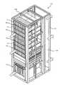
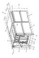
図2は、ラック型記憶制御装置10の外観構成を示す斜視図である。この記憶制御装置10は、例えば、ラック11と、ラック11に着脱可能に取り付けられる複数のハードディスクボックス12と、ラック11の下側に着脱可能に取り付けられる一つのコントローラ13とを備えている。 FIG. 2 is a perspective view showing an external configuration of the rack-type
コントローラ13は、図1中のコントローラ1に対応する。後述のよに、コントローラ13には、2つのクラスタを構成するための論理基板32とバッテリ装置33及び電源供給装置37が設けられており、コントローラ13を正面から見て右半分が一つのクラスタを構成し、左半分が他の一つのクラスタを構成する。各クラスタはそれぞれ冗長構成を備える。従って、バッテリ装置33及び電源供給装置37は、各クラスタ毎に2個ずつ用意されている。 The
ラック11は、収容部11Aと、収容部11Aの後側に設けられる後部空間部11Bとを備える。図2中の白矢印に示すように、冷却風は、ラック11の前面から流入し、ラック11の後面に流出する。 The
図3は、ハードディスクボックス12を後面から見た場合の斜視図である。ハードディスクボックス12は、複数のハードディスクドライブ21を収容している。図3の斜視図では、ハードディスクドライブ21を取り外した状態を示す。ハードディスクボックス12は、前側に位置するドライブ収容部12Aと、後側に位置する電源供給装置12Bとを備える。 FIG. 3 is a perspective view of the
ドライブ収容部12Aには、複数のハードディスクドライブ21が収容される。電源供給装置12B内には、複数の冷却ファン22が設けられている。各ハードディスクドライブ21の全ての面のうち少なくとも前面及び後面には、複数の冷却穴が設けられている。ハードディスクドライブ21の前面から流入した空気は、ハードディスクドライブ21及び電源供給装置12Bをそれぞれ冷却した後、ハードディスクボックス12の後方に排出される。 A plurality of hard disk drives 21 are accommodated in the
なお、本実施例では、ディスクドライブ21としてハードディスクドライブを例に挙げて説明するが、これに限らず、半導体メモリデバイス(フラッシュメモリデバイスを含む)、光ディスクデバイス、光磁気ディスクデバイス、磁気テープデバイス、フレキシブルディスクデバイス等のデータを読み書き可能な種々のデバイスを利用可能である。 In this embodiment, a hard disk drive will be described as an example of the
さらに、記憶デバイスとしてハードディスクデバイスを用いる場合、例えば、FC(Fibre Channel)ディスク、SCSI(Small Computer System Interface)ディスク、SATAディスク、ATA(AT Attachment)ディスク、SAS(Serial Attached SCSI)ディスク等を用いることができる。
半導体メモリデバイスを用いる場合、例えば、フラッシュメモリ、FeRAM(Ferroelectric Random Access Memory)、MRAM(MagnetoresistiveRandom Access Memory)、相変化メモリ(Ovonic Unified Memory)、RRAM(Resistance RAM)」等の種々のメモリデバイスを利用可能である。なお、記憶デバイスの種類は、上記のものに限定されず、将来製品化される他の種類の記憶デバイスを利用することもできるであろう。Furthermore, when using a hard disk device as a storage device, for example, an FC (Fibre Channel) disk, a SCSI (Small Computer System Interface) disk, a SATA disk, an ATA (AT Attachment) disk, a SAS (Serial Attached SCSI) disk, etc. Can do.
When using semiconductor memory devices, use various memory devices such as flash memory, FeRAM (Ferroelectric Random Access Memory), MRAM (Magnetoresistive Random Access Memory), phase change memory (Ovonic Unified Memory), RRAM (Resistance RAM) Is possible. Note that the types of storage devices are not limited to those described above, and other types of storage devices that will be commercialized in the future may be used.
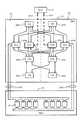
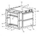
図4は、コントローラ13を前側から見た斜視図である。コントローラ13は、例えば、筐体30と、接続用基板31と、論理基板32と、バッテリ装置33と、冷却ファン34と、ケーブル通路36と、電源供給装置37と、SVP38等を備えている。図4に現れない構成については、別の図と共に後述する。 FIG. 4 is a perspective view of the
筐体30は、ラックマウント型の筐体として構成されており、その前面及び後面が開口している。筐体30の中央部には接続用基板31が設けられている。接続用基板31は、各論理基板32及び各装置33,37,38を電気的に接続するための基板である。接続用基板31によって、筐体30の内部は前後方向に区切られている。接続用基板31の下側には、後述のように下部通路50,51が設けられる。従って、接続用基板31は、例えば、その左右両端が筐体30に固定される。 The
接続用基板31の前面及び後面には、それぞれ複数の論理基板32が着脱可能に設けられている。論理基板32の例については図6と共に後述する。各論理基板32は、図10に示す基板支持部43及び図11に示す基板支持部44に取り付けられる。基板支持部43,44については後述する。 A plurality of
前側の論理基板群の左右両側には、上下2段に重なったバッテリ装置33が設けられている。各バッテリ装置33は、例えば停電時に所定の電力を各論理基板32にそれぞれ供給する。各バッテリ装置33の前面及び下面には、空気を流通させるための複数の冷却穴が設けられている。 On both the left and right sides of the front logic board group,
前後にそれぞれ配置される各論理基板32の上部には、冷却ファン34がそれぞれ設けられている。図4に示すように、前側の論理基板32の上部には、吸い込みファン34が設けられている。図5はコントローラ13を後側から見た斜視図である。図5に示すように、後側の論理基板32の上部には吸い出しファン34が設けられている。吸い込みファンの符号と吸い出しファンの符号とを明確に区別する必要がある場合、吸い込みファンに符号34F、吸い出しファンに符号34Rを与えることができる。同様に、前側の各論理基板32と後側の各論理基板32とを明確に区別する必要がある場合、前側の各論理基板基板に符号32F、後側の各論理基板32に符号32Rを与えることができる。 A cooling
前側の論理基板32の下側には、図11に示すように、第1下部通路51が設けられている。第1下部通路51の前面はパネル35によって施蓋されている。従って、第1下部通路51には、各論理基板32間の隙間から空気が流入する。第1下部通路51には、筐体30の前方の空気は直接流入しない。 As shown in FIG. 11, a first
第1下部通路51の下側には、ケーブル通路36が設けられている。各ケーブルの一端は前側の各論理基板32にそれぞれ接続され、各ケーブルの他端はケーブル通路36を介して、コントローラ13の後方に引き出される。 A
後側の各論理基板32の左右両側には、上下2段に重なった電源供給装置37がそれぞれ設けられている。各電源供給装置37は、各論理基板32に所定電圧の電源をそれぞれ供給する。 On the left and right sides of each
各バッテリ装置33の下側から各電源供給装置37の下側にかけて第2下部通路50が形成されている。第2下部通路50は、第1下部通路51とは分離されている。上段に位置する電源供給装置37の上方とSVP38の下面との間には、接続部40が設けられている。接続部40によって、各バッテリ装置33及び各電源供給装置37を冷却した空気は、各論理基板32を冷却した空気と共に、吸い出しファン34によってコントローラ13の後方に排出される。 A second
接続用基板31は、その前後両面に多数の論理基板32が接続されており、冷却風を通過させるための穴は備えない。しかし、接続用基板31の上側の2つの端部のうち、SVP38内のファン38A(図12参照)に対応する端部には、切り欠き部31Aが設けられている。 The
なお、図4中に示す符号39は、操作パネルである。ユーザは、操作パネル39を操作することにより、コントローラ13に電源を投入して記憶制御装置10を作動させたり、記憶制御装置10の作動を停止させることができる。図4中の符号41,42は、オプション品として搭載される装置を示す。このようなオプション装置としては、例えば、各ハードディスクボックス12の電源供給を制御するための装置を挙げることができる。各オプション装置41,42は、吸い込みファン34の上方に設けられており、前側の各論理基板32の上部に設けられる流入部52(図11参照)と各オプション装置41,42との間は、プレートによって仕切られている。即ち、流入部52には、吸い込みファン34によって吸い込まれた空気が流入し、オプション装置41,42側から空気は流入しないようになっている。 In addition, the code | symbol 39 shown in FIG. 4 is an operation panel. By operating the operation panel 39, the user can turn on the
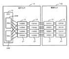
図6は、コントローラ13及びハードディスクボックス12の電気的構成を示すブロック図である。コントローラ13は、ディスクドライブ21を制御するものであるから、DKC(ディスクコントローラ)と呼ぶことができる。ハードディスクボックス12は、複数のディスクドライブ21を収容するものであるから、DKU(ディスクユニット)と呼ぶこともできる。 FIG. 6 is a block diagram showing an electrical configuration of the
論理基板32の例として、例えば、チャネルアダプタ(以下、CHA)基板32A、ディスクアダプタ(以下、DKA)基板32B、キャッシュメモリ(図中、CM)32C、共有メモリ(図中、SM)32D、キャッシュスイッチ(図中、CSW)32Eを挙げることができる。上述の基板のうち、例えば、キャッシュメモリ32Cと共有メモリ32Dとキャッシュスイッチ32Eとは、一つのメモリ制御基板として構成することができる。また、場合によっては、CHA基板32AとDKA基板32Bを一つの制御基板として構成することもできる。なお、NAS(Network Attached Storage)機能を提供するNAS基板を備える構成でもよい。 Examples of the
CHA基板32Aは、第1通信ネットワークCN1を介して、サーバコンピュータやメインフレームコンピュータのようなホストHに接続される。第1通信ネットワークCN1は、例えば、FCP(Fibre Channel Protocol)やiSCSI(internet Small Computer System Interface)のような通信プロトコルを利用するSAN(Storage Area Network)として構成することができる。ホストHがメインフレームコンピュータである場合、例えば、FICON(Fibre Connection:登録商標)、ESCON(Enterprise System Connection:登録商標)、ACONARC(Advanced Connection Architecture:登録商標)、FIBARC(Fibre Connection Architecture:登録商標)等の通信プロトコルを用いることもできる。 The
CHA基板32Aは、ホストHから発行されるリードコマンドやライトコマンドを受領し、その処理結果をホストHに送信する。CHA基板32Aは「第1通信制御基板」に該当する。 The
DKA基板32Bは、第2通信ネットワークCN2を介して、各ハードディスクボックス12内の各ディスクドライブ21と接続される。DKA基板32Bは、各ディスクドライブ21とデータ通信を行うことができる。第2通信ネットワークCN2は、例えば、FCAL(Fibre Channel Arbitrated Loop)のように構成される。 The
キャッシュメモリ32Cは、ホストHから受領したデータやディスクドライブ21から読み出されたデータを一時的に記憶する。共有メモリ32Dは、記憶制御装置10の管理に使用するための各種管理テーブルや制御情報を記憶する。キャッシュスイッチ32Eは、各CHA基板32A及び各DKA基板32Bとキャッシュメモリ32Cとの間のデータ転送を制御する。 The
ここで、簡単にコントローラ13の動作を説明する。ホストHからリードコマンドが発行されると、CHA基板32Aは、このリードコマンドを受領し、共有メモリ32Dにリードコマンドが発行された旨を記憶させる。DKA基板32Bは、共有メモリ32Dを随時参照しており、未処理のリードコマンドを発見すると、そのリードコマンドで要求されたデータを記憶するディスクドライブ21にアクセスして、要求されたデータを読出し、キャッシュメモリ32Cに記憶させる。DKA基板32Bは、リードコマンドで要求されたデータがキャッシュメモリ32Cに記憶された旨を共有メモリ32Dに書き込む。CHA基板32Aは、共有メモリ32Dを随時参照しており、キャッシュメモリ32Cに記憶されたデータを読み出して、ホストHに送信する。 Here, the operation of the
ホストHからライトコマンドが発行された場合、CHA基板32Aは、ライトコマンド及びライトデータを受領し、ライトデータをキャッシュメモリ32Cに記憶させる。CHA基板32Aは、ライトデータをキャッシュメモリ32Cに記憶させた時点で、ホストHにライトコマンドの処理が完了した旨を報告することができる。DKA基板32Bは、タイミングを見計らって、キャッシュメモリ32Cに記憶されたデータをディスクドライブ21に書き込む。なお、DKA基板32Bがライトデータをディスクドライブ21に書き込んだ後で、CHA基板32AがホストHにライトコマンドの処理が完了した旨を通知する構成でもよい。 When a write command is issued from the host H, the
コントローラ13には、2つのクラスタC1,C2が設けられる。各クラスタC1,C2は互いに相手をバックアップしており、いずれか一方のクラスタに障害が発生した場合でも、他方のクラスタによって処理を続行することができる。 The
図7は、クラスタ構成を別の観点から示す説明図である。上述の通り、接続用基板31の前後両面には、同一構成の論理基板群32がそれぞれ設けられている。コントローラ13を正面から見た場合、その右半分と左半分とでそれぞれクラスタが構成される。なお、図7中の矢印は、冷却風の流入方向及び流出方向を示す。しかし、後述のように、コントローラ13内では、冷却風は、U字状に屈曲して流通するようになっている。 FIG. 7 is an explanatory diagram showing the cluster configuration from another viewpoint. As described above, the
図8は、コントローラ13とハードディスクボックス12との接続関係を模式的に示す説明図である。記憶制御装置10には、増設ラック10Aを接続することができる。増設ラック10Aは、ハードディスクボックス12を搭載しており、コントローラ13は搭載していない。各ハードディスクボックス12を接続することにより、より多くのディスクドライブ21をコントローラ13に接続することができる。 FIG. 8 is an explanatory diagram schematically showing the connection relationship between the
図9は、記憶制御装置10の電源供給構成を模式的に示す説明図である。記憶制御装置10内には、複数のPDU14が設けられている。各PDU14は、外部電源をコントローラ13内の各電源供給装置37及びハードディスクボックス12内の各電源供給装置12Bにそれぞれ供給する。電源供給系統も、図9に示すように冗長化されており、いずれか一方の電源供給系統に障害が生じた場合でも、他方の電源供給系統から電源を論理基板32やディスクドライブ21に供給することができる。 FIG. 9 is an explanatory diagram schematically showing a power supply configuration of the
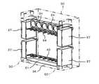
図10〜図14を参照してコントローラ13の機械的構造を説明する。図10は、論理基板32を取り外した状態で、コントローラ13を前面から見た斜視図である。接続用基板31の前後両面には、上下に離間して基板支持部43,44が取り付けられている。 The mechanical structure of the
図10には、下側の基板支持部43が示されている。基板支持部43は、板金等の材料から構成されており、全体として魚の骨のような形状をしている。即ち、基板支持部43は、論理基板32を取り付けるための複数のレール部と、各レール部の間に形成される長方形状の冷却穴とを備えている。上側の基板支持部44も、下側の基板支持部43と同様に構成される。従って、各論理基板32は、2つの基板支持部43,44によって上下から支持されている。なお、下側の基板支持部43の前側にはパネル35が設けられており、第1下部通路51が筐体30の前面に開口するのを防止している。 FIG. 10 shows the lower
なお、上段のバッテリ装置33の上面と筐体30の上面との間には、流路53が形成されている。この流路53は、流入部52と分離して流入部52の上側に設けられており、筐体30の前方から流入する空気をSVP38に供給する。 A
図11は、図10中のXI−XI方向断面図である。矢示F21に示すように、吸い込みファン34を介して流入部52内に流入した空気は、上側の基板支持部44に形成された各冷却穴を介して、各論理基板32間の隙間に流れ込み、各論理基板32を冷却しながら下降する。この空気は、下側の基板支持部43に形成された各冷却穴を介して、第1下部通路50内に流入し、後側の論理基板群に向けて流通する。 11 is a cross-sectional view in the XI-XI direction in FIG. As indicated by an arrow F21, the air that has flowed into the
このように、論理基板32の上下に、論理基板32間の隙間に応じて形成された冷却穴を有する基板支持部43,44をそれぞれ設けることにより、論理基板32を冷却する冷却風の流れの均一化を図ることができる。これにより、U字状に屈曲した第1冷却通路内を流れる冷却風を、ある程度整流することができる。 As described above, by providing the
図12は、図10中のXII−XII方向断面図である。図12では、SVP38を表示している。SVP30の側部には、複数の吸い込みファン38Aが内蔵されている。このファン38Aには、図11に示す流路53を介して空気が供給され、この空気によってSVP38の内部が冷却される。 12 is a cross-sectional view in the XII-XII direction in FIG. In FIG. 12, the
図13は、図10中のXIII−XIII方向断面図である。筐体30の後側では、矢示F22,F23に示すように、冷却風は、第1下部通路51から基板支持部43を介して後側の論理基板4間の隙間に流入する。 13 is a cross-sectional view in the XIII-XIII direction in FIG. On the rear side of the
図14は、図10中のXV−XV方向断面図である。既に説明した通り、筐体30の後側は、多少の相違はあるものの、基本的に筐体30の前側と同一の構成を備えている。主な相違点は、筐体30の前側ではバッテリ装置33が設けられているのに対し、筐体30の後側では電源供給装置37が設けられている点と、筐体30の前側上部にはオプション装置41,42が設けられているのに対し、筐体30の後側上部にはSVP38が設けられている点と、筐体30の前側上部には、SVP38に空気を供給するための流路53が設けられている点と、筐体30の前側のファンは吸い込みファン34として構成されるのに対し、筐体30の後側のファンは吸い出しファン34として構成される点である。 14 is a cross-sectional view in the XV-XV direction in FIG. As described above, the rear side of the
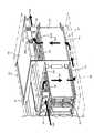
図15〜図18に基づいて、コントローラ13に設けられる複数の冷却通路について説明する。図15は、コントローラ13を正面から見た斜視図である。図16は、図15中のXVI−XVI方向断面図である。図16には、第2冷却通路の構成が示されている。 A plurality of cooling passages provided in the
第2冷却通路は、例えば、前側流路部と、第2下部通路50と、後側流路部と、接続部40とを備えて、略U字状に構成される。前側流路部は、矢示F10に示すように、バッテリ装置33の前面からバッテリ装置33内に流入した空気を、矢示F11に示すように、バッテリ装置33の下側に向けて流出させる。この冷却風F10,F11により、各バッテリ装置33がそれぞれ冷却される。第2下部通路50は、矢示F12に示すように、バッテリ装置33から流入した空気を、筐体30の後側に位置する電源供給装置37の下側まで導く。 The second cooling passage includes, for example, a front channel portion, a second
各電源供給装置37内には、専用の冷却ファン37Aがそれぞれ設けられている。矢示F13に示すように、各ファン37A及び吸い出しファン34によって、第2下部通路50から電源供給装置37内に空気が流入する。 Each
第2下部通路50から電源供給装置37内に流入した空気は、矢示F13,F14に示すように、電源供給装置37内を冷却しながら上昇する。電源供給装置37を冷却した空気は、矢示F15に示すように、電源供給装置37内から接続部40に流入する。SVP38の下面と電源供給装置37の上面との間の空間が接続部40となる。第2冷却通路の空気は、第1冷却通路の下流に流入し、吸い出しファン34を介して、筐体30の外部に排出される。 The air flowing into the
図17は、図15中のXVII−XVII方向断面図である。図17には、第1冷却通路の構成が示されている。第1冷却通路は、例えば、流入部52と、前側流路部と、第1下部通路51と、後側流路部と、流出部52Rとを備えて構成される。 17 is a cross-sectional view in the XVII-XVII direction in FIG. FIG. 17 shows the configuration of the first cooling passage. The first cooling passage includes, for example, an
流入部52は、吸い込みファン34の下流側に位置し、各論理基板32の上部に設けられている。即ち、各論理基板32の上端と筐体30の上面との間の空間が流入部52となっている。矢示F20に示すように、筐体30の前方の空気は、吸い込みファン34を介して流入部52内に流入する。 The
前側流路部は、各論理基板32の間に形成される。上述の通り、各論理基板32は、上下に配置された基板支持部43,44のレール部にそれぞれ取り付けられており、かつ、各レール部の間には冷却穴が形成されている。従って、各論理基板32の間には、機械的に定まる隙間が形成される。この隙間が前側流路となる。矢示F21に示すように、流入部52内の空気は、各論理基板32を冷却しながら下向きに流れる。 The front channel portion is formed between the
各論理基板32間の隙間を下降した空気は、第1下部通路51内に流入し、矢示F22に示すように、後側の各論理基板32の下側に向けて流れる。第1冷却通路51内の空気は、矢示F23に示すように、後側の各論理基板32間の隙間にそれぞれ流れ込み、各論理基板32を冷却しながら上昇する。 The air descending through the gaps between the
後側の各論理基板32を冷却した空気は、流出部52Rに流入し、矢示F24に示すように、吸い出しファン34によって筐体30の後方に排出される。 The air that has cooled each
図18は、図15中のXVIII−XVIII方向断面図である。図18には、第3冷却通路及びSVPに供給される冷却風の様子がそれぞれ示されている。第3冷却通路は、図16で述べた第2冷却通路と同様に構成される。 18 is a cross-sectional view in the XVIII-XVIII direction in FIG. FIG. 18 shows the state of the cooling air supplied to the third cooling passage and the SVP. The third cooling passage is configured similarly to the second cooling passage described in FIG.
各バッテリ装置33内に流入した空気(F30)は、各バッテリ装置33を冷却しながら下降し(F31)、第2下部通路50内に流入する。空気は、第2下部通路50を介して電源供給装置37の下側に移動し(F32)、ファン37Aによって電源供給装置37内に吸い込まれる(F33)。空気は、各電源供給装置37を冷却しながら上昇し(F34)、接続部40に流入する(F35)。接続部40に流入したの空気は、吸い出しファン34によって、筐体30の後方に排出される。 The air (F30) flowing into each
SVP38の冷却について説明する。本実施例のSVP38は、内蔵ファン38Aが筐体30の右側に位置するようにして、筐体30の上側に水平に載置されている。図15に示すように、吸い込みファン34の上側と筐体30の上面との間には、流路53が形成されている。流路53を介して筐体30内に流入した空気は(F40)、接続用基板31の切り欠き部31Aを介してSVP38の右側面に移動し(F41)、内蔵ファン38AによってSVP38内に吸い込まれる(F42)。SVP38を冷却した空気は、SVP38の左側面に設けられる冷却穴を介して、筐体30の外部に排出される(F43)。 The cooling of the
上述のように本実施例では、前後にそれぞれ配置された各論理基板32と、右側のバッテリ装置33及び電源供給装置37と、左側のバッテリ装置33及び電源供給装置37と、SVP38とを、それぞれ個別の冷却通路によって冷却することができ、冷却効率を改善することができる。例えば、発熱量の比較的大きい論理基板32は比較的大きな風量で冷却し、発熱量の比較的小さいバッテリ装置33や電源供給装置37は比較的少ない風量で冷却できる。 As described above, in the present embodiment, each of the
ここで留意すべき点は、本実施例では、筐体30の前側に配置された冷却対象(論理基板32,バッテリ装置33,電源供給装置37)は、上側から下側に向けて流れる空気によって冷却されるのに対し、筐体30の後側に配置された同様の冷却対象は、下側から上側に向けて流れる空気によって冷却される点である。つまり、前側の冷却対象と後側の冷却対象とでは、その冷却風の流れる方向が異なる。 It should be noted that in this embodiment, the cooling target (
本実施例では、水平方向に流入した空気を下降させながら筐体30の前側に位置する冷却対象を冷却させ、次に、この空気を下部通路50,51によって筐体30の後側に導いて上昇させ、筐体30の後側に位置する冷却対象を冷却させ、最後に、筐体30の後方に排出させる。即ち、本実施例では、筐体30内に、略U字状またはΩの文字を上下逆にした形状の屈曲した冷却通路を設ける。これにより、本実施例の接続用基板31には、冷却風を水平方向に通過させるための冷却穴を設ける必要がなく、接続用基板31の面積を電気的接続のために効率的に使用することができる。従って、本実施例では、接続用基板31の前後両面に、より多くの論理基板32を取り付けることができ、規格化された狭い空間内に高密度で論理基板32等を設けることができる。 In this embodiment, the cooling target located on the front side of the
また、上記の屈曲した冷却通路によって、上下に重ねられた複数のバッテリ装置33及び電源供給装置37を冷却することができる。 Further, the plurality of
本実施例では、前側の各論理基板32に接続されるケーブルを通すためのケーブル通路36を、第1下部通路51の下側に別に設ける。従って、第1下部通路51内の空気の流れを阻害することなく、ケーブルをラック11の後方に引き出すことができる。これにより、保守作業の作業性が向上する。 In the present embodiment, a
本実施例では、筐体30の前側にバッテリ装置33を、筐体30の後側に電源供給装置37をそれぞれ配置させる。PDU14に接続される電源供給装置37を筐体30の後側に配置することにより、より簡単に電源供給装置37とPDU14とを電源ケーブルで接続することができ、構成を簡素化できる。 In this embodiment, the
本実施例では、筐体30の正面から見て左右のバッテリ装置33と電源供給装置37とでそれぞれペアを構成し、各ペア毎に冷却通路を設ける。換言すれば、バッテリ装置33を冷却するための流路と電源供給装置37を冷却するための流路とを共通にする。これにより、電源供給装置37内の冷却ファン37Aによって、バッテリ装置33及び電源供給装置37を冷却できる。従って、バッテリ装置33内に冷却ファンを設ける必要がなく、製造コストを低減できる。 In the present embodiment, the left and
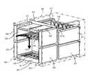
さらに、本実施例では、論理基板32,バッテリ装置33,電源供給装置37,SVP38を、大型記憶制御装置の構成部品としても使用可能である。図19は、参考例として示す大型記憶制御装置100の斜視図である。 Further, in this embodiment, the
大型記憶制御装置100は、例えば、フレーム本体110と、フレーム本体110の中央部に設けられる中央冷却通路111と、中央冷却ファン群130と、上部冷却ファン群131とを備える。フレーム本体110の下側には、バッテリ装置33及び電源供給装置37が設けられ、フレーム本体110の中央部にはコントローラ13が設けられ、フレーム本体110の上部にはハードディスクボックス12が設けられる。これらコントローラ13やハードディスクボックス12、バッテリ装置33及び電源供給装置37は、それぞれ中央冷却通路111を挟んで背中合わせに配置される。即ち、中央冷却通路111を挟む前面と後面とに、それぞれコントローラ13やハードディスクボックス12等が設けられる。図20に示すように、前面の構成部品によって一つのクラスタが構成され、後面の構成部品によって他の一つのクラスタが構成される。 The large-sized
論理基板32,バッテリ装置33,電源供給装置37,SVP38の設置方向等を変えるだけで、大型記憶制御装置100に使用することができる。これにより、本実施例では、ラック型記憶制御装置10と大型記憶制御装置100とで主要部品を共通化することができ、開発及び設計に要するコスト、製造コスト、在庫管理コスト等を低減できる。 It can be used for the large-sized
なお、本発明は、上述した実施の形態に限定されない。当業者であれば、本発明の範囲内で、種々の追加や変更等を行うことができる。例えば、SVPは筐体の前側の上部に設けることもできる。 The present invention is not limited to the above-described embodiment. A person skilled in the art can make various additions and changes within the scope of the present invention. For example, the SVP can be provided in the upper part on the front side of the housing.
1…コントローラ、2…筐体、3…接続用基板 、4…論理基板、5…バッテリ装置、6…冷却ファン、7A,7B…下部通路、7C…ケーブル通路、8…電源供給装置、8A…冷却ファン、9…SVP(サービスプロセッサ)、10…ラック型記憶制御装置、10A…増設ラック、11…ラック、11A…収容部、11B…後部空間部、12…ハードディスクボックス、12A…ドライブ収容部、12B…電源供給装置、13…コントローラ、21…ディスクドライブ、22…冷却ファン、30…筐体、31…接続用基板、31A…切り欠き部、32…論理基板、32A…チャネルアダプタ基板、32B…ディスクアダプタ基板、32C…キャッシュメモリ、32D…共有メモリ、32E…キャッシュスイッチ、33…バッテリ装置、34…冷却ファン、35…パネル、36…ケーブル通路、37…電源供給装置、37A…冷却ファン、38…SVP、38A…冷却ファン、39…操作パネル、41,42…オプション装置、43…基板支持部、50…第2下部通路、51…第1下部通路、52…流入部、52R…流出部、53…流路、100…大型記憶制御装置、110…フレーム本体、111…中央冷却通路、130…中央冷却ファン群、131…上部冷却ファン群、C1,C2…クラスタ DESCRIPTION OF
Claims (14)
Translated fromJapanese前面及び後面がそれぞれ開口する筐体と、
前記筐体の内部を前後に分割するようにして前記筐体の中央部に設けられる接続用基板と、
前記筐体の前面側及び後面側にそれぞれ設けられ、記憶デバイスに関する制御を実行するための複数の制御基板を含む制御基板群と、
前記各制御基板群の左右両側にそれぞれ設けられる電源関連装置と、
前記各制御基板群を第1冷却風によってそれぞれ冷却する第1冷却通路と、
前記各電源関連装置のうち前記各制御基板群の一側に位置する電源関連装置を第2冷却風によってそれぞれ冷却する第2冷却通路と、
前記各電源関連装置のうち前記各制御基板群の他側に位置する電源関連装置を第3冷却風によってそれぞれ冷却するための第3冷却通路と、を備え、
前記第1冷却通路の流入口には吸い込みファンが、前記第1冷却通路の流出口には吸い出しファンがそれぞれ設けられており、
前記吸い込みファンは、前記各制御基板群のうち前記筐体の前面側に位置する前側制御基板群の上側に設けられており、前記吸い出しファンは、前記各制御基板群のうち前記筐体の後面側に位置する後側制御基板群の上側に設けられており、
前記第1冷却通路は、前記吸い込みファンの下流側に位置して前記前側制御基板群の上部に設けられる流入部と、この流入部に連通して設けられ、前記前側制御基板群を構成する各制御基板間に形成される前側流路部と、この前側流路部に連通して設けられ、前記筐体の前面側から後面側にわたって前記筐体の下側に形成される第1下部通路と、この第1下部通路に連通して設けられ、前記後側制御基板群を構成する各制御基板間に形成される後側流路部と、この後側流路部に連通して、前記吸い出しファンの上流側に位置して前記後側制御基板群の上部に設けられる流出部と、を備えて構成され、
前記第2冷却通路及び前記第3冷却通路は、前記各電源関連装置のうち前記筐体の前面側に位置する前側電源関連装置内に設けられ、この前側電源関連装置の前面から流入する空気を下側に向けて流出させる前側流路部と、この前側流路部に連通して設けられ、前記筐体の前面側から後面側にわたって前記筐体の下側に形成される第2下部通路と、この第2下部通路に連通して、前記各電源関連装置のうち前記筐体の後面側に位置する後側電源関連装置内に設けられ、前記第2下部通路から流入する空気を上側に向けて流出させる後側流路部と、この後側流路部と前記第1冷却通路の前記流出部とを連通させるようにして、前記後側電源関連装置の上部に設けられる接続部と、を備えて構成される、
ラックマウント型制御装置の冷却構造。
A cooling structure for a rack mount type control device,
A housing whose front and rear surfaces each open;
A connection board provided in a central portion of the casing so as to divide the interior of the casing into front and rear,
A control board group including a plurality of control boards provided on the front side and the rear side of the housing, respectively, for executing control related to the storage device;
Power supply-related devices respectively provided on the left and right sides of each control board group;
A first cooling passage for cooling each control board group with a first cooling air;
A second cooling passage for cooling each power supply related device located on one side of each control board group among the power supply related devices by a second cooling air;
A third cooling passage for cooling each power supply related device located on the other side of each control board group with a third cooling air,
A suction fan is provided at the inlet of the first cooling passage, and a suction fan is provided at the outlet of the first cooling passage;
The suction fan is provided on the upper side of the front control board group located on the front side of the casing among the control board groups, and the suction fan is a rear surface of the casing among the control board groups. Provided on the upper side of the rear control board group located on the side,
The first cooling passage is located on the downstream side of the suction fan and is provided in an upper part of the front control board group, and is provided in communication with the inflow part, and each of the front control board groups A front flow path portion formed between the control substrates, and a first lower passage provided in communication with the front flow path portion and formed on the lower side of the casing from the front side to the rear side of the casing; A rear flow path portion provided between the control boards constituting the rear control board group and communicating with the first lower passage; and communicating with the rear flow path section to An outflow portion that is located on the upstream side of the fan and is provided on the upper portion of the rear control board group,
The second cooling passage and the third cooling passage are provided in a front power supply related device located on the front side of the casing among the power supply related devices, and air flowing from the front of the front power supply related device is provided. A front-side flow channel portion that flows out toward the lower side, a second lower passage that is provided in communication with the front-side flow channel portion and is formed on the lower side of the housing from the front surface side to the rear surface side of the housing; The second lower passage communicates with the second lower passage and is provided in a rear power-related device located on the rear side of the casing among the power-related devices, and the air flowing in from the second lower passage is directed upward. A rear flow path portion that is allowed to flow out, and a connection portion that is provided at an upper portion of the rear power supply related device so as to communicate with the rear flow path portion and the outflow portion of the first cooling passage. Composed of,
Cooling structure ofLa Kkumaunto type controller.
The cooling structure for a rack mount control device according to claim1 , wherein the first lower passage and the second lower passage are provided independently so that air does not flow.
The cooling structure of the rack mount type control device according to claim1 , wherein the rear power supply related device includes a cooling fan.
The cooling structure for a rack mount type control device according to claim1 , wherein the front power-related device is a battery device, and the rear power-related device is a power supply device.
Substrate support parts for supporting the control boards constituting the control board groups are provided on the connection board, which are located at both upper and lower ends of the control board groups, and the board support parts include the cooling structure of the cooling holes for circulating air between the control board is provided, rack-mounted control device of claim1.
Between the inner surface of the lower side to the casing of the first lower passage, the cable passage for connecting the cable to the each control substrate constituting the front control substrate group is provided, in claim1 The cooling structure of the rack-mount type control apparatus described.
A plurality of the front power supply related devices are provided on each of the left and right sides of the front control board group, and a plurality of the rear power supply related devices are provided on the left and right sides of the rear control board. The cooling structure of the rack-mount type control apparatus according to claim1 .
Each of the front-side power-related devices is positioned on both the left and right sides of the front-side control board group, and is provided in two upper and lower layers so that air can flow. The cooling structure for a rack-mounted control device according to claim7 , wherein the cooling structure is positioned on both the left and right sides of the side control board group and is stacked in two upper and lower stages so that air can flow.
Of each control board group and each power supply related device, a first cluster is configured by each control board group and each power supply related device belonging to the left half of the casing, and each control board group and each power supply related device The cooling structure of the rack-mounted control device according to claim 1, wherein a second cluster is configured by each control board group and each power-related device belonging to the right half of the casing of the device.
The cooling structure of the rack mount type control device according to claim 1, wherein a management device for managing the control device is provided horizontally on either the front upper portion or the rear upper portion of the housing.
The cooling structure for a rack-mounted control device according to claim 1, wherein each control board group and each power-related device are configured to be diverted as they are to a housing having a structure different from that of the rack.
前記制御装置は、
前記ラックに収容されるラックマウント型の筐体と、
前記筐体の内部を前後に分割するようにして前記筐体の中央部に設けられる接続用基板と、
前記筐体の前面側及び後面側にそれぞれ設けられる制御基板群であって、データ入出力を要求するコマンドを発行する装置との間の通信を担当する第1通信制御基板と、前記各記憶デバイスとの間の通信を担当する第2通信制御基板と、前記第1通信制御基板及び前記第2通信制御基板にメモリ領域をそれぞれ提供するメモリ制御基板とを含む制御基板群と、
前記各制御基板群を上下両端からそれぞれ支持する基板支持部であって、前記各制御基板群を構成する制御基板間に空気を流通させる複数の冷却穴を有する基板支持部と、
前記各制御基板群のうち前記筐体の前面側に位置する前側制御基板群の左右両側に上下2段に重ねてそれぞれ配置されるバッテリ装置と、
前記各制御基板群のうち前記筐体の後面側に位置する後側制御基板群の左右両側に上下2段に重ねてそれぞれ配置される電源供給装置であって、冷却ファンを内蔵する電源供給装置と、
前記前側制御基板群の上部に設けられる吸い込みファンと、
前記後側制御基板群の上部に設けられる吸い出しファンと、
前記各制御基板群を冷却するための第1冷却通路であって、前記吸い込みファンの下流側に位置して前記前側制御基板群の上部に設けられる流入部と、この流入部に連通して設けられ、前記基板支持部の前記各冷却穴と前記前側制御基板群を構成する各制御基板間の隙間とによって形成される前側流路部と、この前側流路部に連通して設けられ、前記筐体の前面側から後面側にわたって前記筐体の下側に形成される第1下部通路と、この第1下部通路に連通して設けられ、前記基板支持部の前記各冷却穴と前記後側制御基板群を構成する各制御基板間の隙間とによって形成される後側流路部と、この後側流路部に連通して、前記吸い出しファンの上流側に位置して前記後側制御基板群の上部に設けられる流出部と、を備える第1冷却通路と、
前記筐体の左側に位置する前記バッテリ装置及び前記電源供給装置をそれぞれ冷却するための第2冷却通路であって、前記バッテリ装置の前面から流入する空気を下側に向けて流出させる前側流路部と、この前側流路部に連通して設けられ、前記筐体の前面側から後面側にわたって前記筐体の下側に形成される第2下部通路と、この第2下部通路に連通して、前記電源供給装置内に設けられ、前記第2下部通路から流入する空気を上側に向けて流出させる後側流路部と、この後側流路部と前記第1冷却通路の前記流出部とを連通させるようにして、前記電源供給装置の上部に設けられる接続部と、を備える第2冷却通路と、
前記筐体の右側に位置する前記バッテリ装置及び前記電源供給装置をそれぞれ冷却するための第3冷却通路であって、前記バッテリ装置の前面から流入する空気を下側に向けて流出させる前側流路部と、この前側流路部に連通して設けられ、前記筐体の前面側から後面側にわたって前記筐体の下側に形成される第2下部通路と、この第2下部通路に連通して、前記電源供給装置内に設けられ、前記第2下部通路から流入する空気を上側に向けて流出させる後側流路部と、この後側流路部と前記第1冷却通路の前記流出部とを連通させるようにして、前記電源供給装置の上部に設けられる接続部と、を備える第3冷却通路と、
前記第1下部通路の下側と前記筐体の内面との間に設けられ、前記前側制御基板群を構成する前記各制御基板にケーブルを接続するためのケーブル通路と、
を備えるラック型記憶制御装置。
A rack, a plurality of storage device storage devices detachably provided in the rack, and a control for controlling a plurality of storage devices provided in the rack and detachably provided in the storage device storage devices A rack-type storage control device comprising:
The controller is
A rack-mountable housing housed in the rack;
A connection board provided in a central portion of the casing so as to divide the interior of the casing into front and rear,
A control board group provided on each of the front side and the rear side of the housing, the first communication control board in charge of communication with a device that issues a command requesting data input / output; and each storage device A control board group including a second communication control board in charge of communication between the first communication control board and a memory control board that provides a memory area to each of the first communication control board and the second communication control board;
A substrate support part for supporting each control board group from both upper and lower ends, and a substrate support part having a plurality of cooling holes for circulating air between the control boards constituting each control board group;
Battery devices respectively arranged in two upper and lower layers on the left and right sides of the front control board group located on the front side of the housing among the control board groups;
A power supply device arranged in two upper and lower stages on each of the left and right sides of a rear control board group located on the rear surface side of the housing among the control board groups, the power supply device having a built-in cooling fan When,
A suction fan provided on top of the front control board group;
A suction fan provided on top of the rear control board group;
A first cooling passage for cooling each of the control board groups, and an inflow portion that is located on the downstream side of the suction fan and is provided on an upper portion of the front control board group, and is provided in communication with the inflow portion. A front channel portion formed by each cooling hole of the substrate support portion and a gap between the control substrates constituting the front control substrate group, and provided in communication with the front channel portion, A first lower passage formed on the lower side of the housing from the front surface side to the rear surface side of the housing, and provided in communication with the first lower passage, and each cooling hole of the substrate support portion and the rear side A rear flow path portion formed by a gap between the control boards constituting the control board group, and the rear control board that communicates with the rear flow path portion and is located upstream of the suction fan. A first cooling passage comprising an outflow portion provided at the top of the group;
A second cooling passage for cooling the battery device and the power supply device located on the left side of the housing, respectively, and a front flow path for discharging air flowing in from the front surface of the battery device downward And a second lower passage provided on the lower side of the casing from the front side to the rear side of the casing, and in communication with the second lower passage. A rear flow path portion provided in the power supply device for flowing out the air flowing in from the second lower passage upward, and the rear flow path portion and the outflow portion of the first cooling passage. A second cooling passage provided with a connection portion provided at an upper part of the power supply device,
A third cooling passage for cooling the battery device and the power supply device located on the right side of the housing, respectively, and a front-side flow channel that causes air flowing in from the front surface of the battery device to flow out downward And a second lower passage provided on the lower side of the casing from the front side to the rear side of the casing, and in communication with the second lower passage. A rear flow path portion provided in the power supply device for flowing out the air flowing in from the second lower passage upward, and the rear flow path portion and the outflow portion of the first cooling passage. A third cooling passage provided with a connection portion provided at an upper part of the power supply device so as to communicate with each other,
A cable path provided between the lower side of the first lower path and the inner surface of the housing, and for connecting a cable to each control board constituting the front control board group;
A rack-type storage control device.
The rack according to claim12 , wherein the connection board is not provided with a cooling hole for actively circulating air before and after the casing in a range where at least the control board groups are connected. Type storage controller.
前記管理装置に冷却風を供給するための第4冷却通路が、前記第1、第2、第3冷却通路とは独立して、前記筐体の上部に設けられている請求項12に記載のラック型記憶制御装置。
A management device for collecting and managing information on the state of the control device from each control board is placed in the upper part of the housing in the horizontal direction.
Fourth cooling passage for supplying cooling air to said management apparatus, said first, second, and third cooling passages independently, according to claim12 provided in an upper portion of the housing Rack type storage controller.
Priority Applications (3)
| Application Number | Priority Date | Filing Date | Title |
|---|---|---|---|
| JP2007220647AJP4898598B2 (en) | 2007-08-28 | 2007-08-28 | Cooling structure of rack mount type control device and rack type storage control device |
| US12/068,297US7701710B2 (en) | 2007-08-28 | 2008-02-05 | Cooling structure for rackmount-type control device and rack-type storage control device |
| US12/659,520US7933120B2 (en) | 2007-08-28 | 2010-03-11 | Cooling structure for rackmount-type control device and rack-type storage control device |
Applications Claiming Priority (1)
| Application Number | Priority Date | Filing Date | Title |
|---|---|---|---|
| JP2007220647AJP4898598B2 (en) | 2007-08-28 | 2007-08-28 | Cooling structure of rack mount type control device and rack type storage control device |
Publications (2)
| Publication Number | Publication Date |
|---|---|
| JP2009053978A JP2009053978A (en) | 2009-03-12 |
| JP4898598B2true JP4898598B2 (en) | 2012-03-14 |
Family
ID=40407128
Family Applications (1)
| Application Number | Title | Priority Date | Filing Date |
|---|---|---|---|
| JP2007220647AExpired - Fee RelatedJP4898598B2 (en) | 2007-08-28 | 2007-08-28 | Cooling structure of rack mount type control device and rack type storage control device |
Country Status (2)
| Country | Link |
|---|---|
| US (2) | US7701710B2 (en) |
| JP (1) | JP4898598B2 (en) |
Cited By (1)
| Publication number | Priority date | Publication date | Assignee | Title |
|---|---|---|---|---|
| KR101438723B1 (en)* | 2012-06-05 | 2014-09-05 | 이동학 | Cooling system of a computer having a gpu |
Families Citing this family (70)
| Publication number | Priority date | Publication date | Assignee | Title |
|---|---|---|---|---|
| JP5003875B2 (en)* | 2007-03-01 | 2012-08-15 | 日本電気株式会社 | Cooling mechanism |
| JP4898598B2 (en)* | 2007-08-28 | 2012-03-14 | 株式会社日立製作所 | Cooling structure of rack mount type control device and rack type storage control device |
| JP4798287B2 (en)* | 2008-02-06 | 2011-10-19 | パナソニック株式会社 | Electrical equipment |
| US9426903B1 (en) | 2008-06-27 | 2016-08-23 | Amazon Technologies, Inc. | Cooling air stack for computer equipment |
| US7826222B2 (en) | 2008-07-03 | 2010-11-02 | Juniper Networks, Inc. | Front-to-back cooling system for modular systems with orthogonal midplane configuration |
| JP2010039826A (en)* | 2008-08-06 | 2010-02-18 | Hitachi Ltd | Storage apparatus, fan device and controller unit device |
| JP4727709B2 (en)* | 2008-11-12 | 2011-07-20 | 株式会社日立製作所 | Storage controller |
| JP4693891B2 (en)* | 2008-11-12 | 2011-06-01 | 株式会社日立製作所 | Storage controller |
| US7804684B1 (en) | 2008-12-22 | 2010-09-28 | Juniper Networks, Inc. | Cooling system for a data processing unit |
| DE102009020390B3 (en)* | 2009-05-08 | 2010-05-20 | Sinitec Vertriebsgesellschaft Mbh | Server frame and suitable insert server for use in the server frame |
| JP4662315B2 (en)* | 2009-05-20 | 2011-03-30 | 株式会社安川電機 | Fan unit and electronic device equipped with the same |
| JP5243614B2 (en)* | 2009-06-26 | 2013-07-24 | 株式会社日立製作所 | Storage device, storage controller of storage device, and housing for storage controller |
| US8534930B1 (en) | 2009-09-24 | 2013-09-17 | Juniper Networks, Inc. | Circuit boards defining openings for cooling electronic devices |
| US20110085296A1 (en)* | 2009-10-14 | 2011-04-14 | Brandon Rubenstein | Cooling System For A Computer Blade |
| JP5337723B2 (en)* | 2010-01-13 | 2013-11-06 | アラクサラネットワークス株式会社 | Electronic equipment |
| US8279601B2 (en)* | 2010-01-28 | 2012-10-02 | Juniper Networks, Inc. | Air flow ducts for cooling electronic devices within a data processing unit |
| US8154867B2 (en)* | 2010-03-10 | 2012-04-10 | Ciena Corporation | High density switching platform with interbay connections arrangement |
| US8638553B1 (en) | 2010-03-31 | 2014-01-28 | Amazon Technologies, Inc. | Rack system cooling with inclined computing devices |
| US8755192B1 (en) | 2010-03-31 | 2014-06-17 | Amazon Technologies, Inc. | Rack-mounted computer system with shock-absorbing chassis |
| US9622387B1 (en) | 2010-03-31 | 2017-04-11 | Amazon Technologies, Inc. | Rack-mounted air directing device with scoop |
| US9894808B2 (en) | 2010-03-31 | 2018-02-13 | Amazon Technologies, Inc. | Compressed air cooling system for data center |
| WO2011141950A1 (en)* | 2010-05-10 | 2011-11-17 | Hitachi, Ltd. | Storage apparatus |
| US8918573B2 (en) | 2010-06-23 | 2014-12-23 | International Business Machines Corporation | Input/output (I/O) expansion response processing in a peripheral component interconnect express (PCIe) environment |
| US20110317351A1 (en)* | 2010-06-23 | 2011-12-29 | International Business Machines Corporation | Server drawer |
| US8745292B2 (en) | 2010-06-23 | 2014-06-03 | International Business Machines Corporation | System and method for routing I/O expansion requests and responses in a PCIE architecture |
| US8645767B2 (en) | 2010-06-23 | 2014-02-04 | International Business Machines Corporation | Scalable I/O adapter function level error detection, isolation, and reporting |
| US8472183B1 (en)* | 2010-09-20 | 2013-06-25 | Amazon Technologies, Inc. | Rack-mounted computer system with front-facing power supply unit |
| US8477491B1 (en)* | 2010-09-20 | 2013-07-02 | Amazon Technologies, Inc. | System with rack-mounted AC fans |
| US10492331B1 (en) | 2010-09-29 | 2019-11-26 | Amazon Technologies, Inc. | System and method for cooling power distribution units |
| TWM419141U (en)* | 2011-08-11 | 2011-12-21 | Quanta Comp Inc | Server system |
| JP5677245B2 (en)* | 2011-09-13 | 2015-02-25 | 株式会社東芝 | Electronics |
| US9095070B2 (en) | 2011-12-05 | 2015-07-28 | Amazon Technologies, Inc. | Partial-width rack-mounted computing devices |
| US8773861B2 (en) | 2011-12-15 | 2014-07-08 | Amazon Technologies, Inc. | Reconfigurable shelf for computing modules |
| US8867214B2 (en) | 2011-12-15 | 2014-10-21 | Amazon Technologies, Inc. | Modular server design for use in reconfigurable server shelf |
| US8720043B2 (en) | 2011-12-15 | 2014-05-13 | Amazon Technologies, Inc. | Method of allocating resources in a rack system |
| US8988877B2 (en) | 2011-12-22 | 2015-03-24 | Lenovo Enterprise Solutions (Singapore) Pte. Ltd. | Automatic coupling of independent cooling regions during fan maintenance |
| US8913391B2 (en)* | 2012-01-30 | 2014-12-16 | Alcatel Lucent | Board-level heat transfer apparatus for communication platforms |
| US9408330B2 (en)* | 2012-04-18 | 2016-08-02 | International Business Machines Coporation | Apparatus to cool a computing device |
| US10082857B1 (en) | 2012-08-07 | 2018-09-25 | Amazon Technologies, Inc. | Cooling electrical systems based on power measurements |
| US9253927B1 (en) | 2012-09-28 | 2016-02-02 | Juniper Networks, Inc. | Removable fan tray |
| CN104603881B (en)* | 2012-10-18 | 2017-03-08 | 株式会社日立制作所 | Storage device and storage controller of said storage device |
| US9894809B1 (en) | 2013-02-28 | 2018-02-13 | Amazon Technologies, Inc. | System for supplying cooling air from sub-floor space |
| DE112013006344T5 (en) | 2013-03-26 | 2015-09-17 | Hitachi, Ltd. | Storage device and method for producing a housing for receiving containers |
| US10037061B1 (en) | 2013-04-30 | 2018-07-31 | Amazon Technologies, Inc. | Multiple-stage cooling system for rack |
| US9261925B1 (en)* | 2013-09-25 | 2016-02-16 | Emc Corporation | Optimized server design using dense DIMM spacing, wide heatsink, improved routing channels, and improved air delivery to rear devices |
| KR101405501B1 (en) | 2013-10-08 | 2014-06-11 | (주) 인프론티브 | Rack mounted computing device |
| US9203782B2 (en) | 2013-11-20 | 2015-12-01 | Ciena Corporation | High density networking shelf and system |
| US9167725B2 (en)* | 2013-12-25 | 2015-10-20 | Super Micro Computer Inc. | Backplane structure and server system utilizing the same |
| JP6262590B2 (en)* | 2014-03-31 | 2018-01-17 | 高砂熱学工業株式会社 | Air conditioning system for rooms containing information communication equipment |
| US9578786B1 (en)* | 2014-06-10 | 2017-02-21 | Amazon Technologies, Inc. | Computer system with bypass air plenum |
| WO2016175799A1 (en)* | 2015-04-29 | 2016-11-03 | Hewlett Packard Enterprise Development Lp | Converged infrastructure manager |
| US9832912B2 (en) | 2015-05-07 | 2017-11-28 | Dhk Storage, Llc | Computer server heat regulation utilizing integrated precision air flow |
| US9817450B2 (en)* | 2015-07-22 | 2017-11-14 | Celestica Technology Consultancy (Shanghai) Co. Ltd | Electronic apparatus |
| US9405336B1 (en)* | 2015-09-12 | 2016-08-02 | Qingyuan Li | Silent computers having external heat sinks and portable raid docks |
| US10624241B1 (en) | 2015-10-06 | 2020-04-14 | Amazon Technologies, Inc. | Rack mountable thermal regulation system |
| US10368466B1 (en) | 2015-10-06 | 2019-07-30 | Amazon Technologies, Inc. | Rack mountable cooling canister |
| US9642286B1 (en) | 2015-12-14 | 2017-05-02 | Amazon Technologies, Inc. | Coordinated control using rack mountable cooling canisters |
| US10321608B1 (en)* | 2015-12-14 | 2019-06-11 | Amazon Technologies, Inc. | Coordinated cooling using rack mountable cooling canisters |
| US10271460B2 (en)* | 2016-01-11 | 2019-04-23 | Quanta Computer Inc. | Server system |
| US9603289B1 (en) | 2016-01-14 | 2017-03-21 | Ciena Corporation | Chassis arrangement systems and methods for dual depth cards and dual depth faraday cages |
| JP6809111B2 (en)* | 2016-10-11 | 2021-01-06 | 富士通株式会社 | Electronic equipment cooling unit |
| US10390462B2 (en)* | 2017-02-16 | 2019-08-20 | Dell Products, Lp | Server chassis with independent orthogonal airflow layout |
| US10856436B2 (en) | 2019-01-31 | 2020-12-01 | Seagate Technology Llc | Multilevel enclosure cooling |
| US11980009B2 (en) | 2019-10-15 | 2024-05-07 | Ciena Corporation | Liquid cooling high-density pluggable modules for a network element |
| US11184995B2 (en) | 2019-11-01 | 2021-11-23 | Ciena Corporation | High-density network element cooling via unequipped pluggable optical module cages |
| US11112573B2 (en) | 2019-11-01 | 2021-09-07 | Ciena Corporation | Cooling multiple high-density network pluggable optical modules using a shared heat exchanger |
| JP7065908B2 (en)* | 2020-06-16 | 2022-05-12 | 株式会社日立製作所 | Storage device |
| US11550370B2 (en) | 2020-10-30 | 2023-01-10 | Seagate Technology Llc | Modular data storage systems |
| US11653478B1 (en)* | 2021-04-19 | 2023-05-16 | Advanced Thermal Solutions, Inc. | Stackable enclosure system with cooling features, and related apparatus and methods |
| JP2025030478A (en)* | 2023-08-23 | 2025-03-07 | 三菱重工業株式会社 | Converter, conversion unit, and storage panel |
Family Cites Families (24)
| Publication number | Priority date | Publication date | Assignee | Title |
|---|---|---|---|---|
| US5027254A (en)* | 1989-11-09 | 1991-06-25 | International Business Machines Corporation | Apparatus for cooling electronics components |
| US5497288A (en)* | 1994-08-31 | 1996-03-05 | International Business Machines Corporation | Apparatus for tilted serial cooling in an electronic system |
| US5825620A (en)* | 1996-12-18 | 1998-10-20 | International Business Machines Corporation | Enhanced air cooling system with attached cooling unit |
| US5963425A (en)* | 1997-07-16 | 1999-10-05 | International Business Machines Corporation | Combined air and refrigeration cooling for computer systems |
| US5949646A (en)* | 1998-07-31 | 1999-09-07 | Sun Microsystems, Inc. | Compact computer having a redundant air moving system and method thereof |
| JP4108472B2 (en)* | 2000-07-25 | 2008-06-25 | 富士通株式会社 | Disk array unit |
| US6950895B2 (en)* | 2001-06-13 | 2005-09-27 | Intel Corporation | Modular server architecture |
| JP3652634B2 (en)* | 2001-10-05 | 2005-05-25 | 本田技研工業株式会社 | Cooling structure for high piezoelectric parts |
| US6594148B1 (en)* | 2002-01-16 | 2003-07-15 | Cisco Technology, Inc. | Airflow system |
| US7075788B2 (en)* | 2003-06-11 | 2006-07-11 | Hewlett-Packard Development Company, L.P. | Computer cooling system and method |
| US7079387B2 (en)* | 2003-06-11 | 2006-07-18 | Hewlett-Packard Development Company, L.P. | Computer cooling system and method |
| US6927975B2 (en)* | 2003-06-27 | 2005-08-09 | International Business Machines Corporation | Server blade modular chassis mechanical and thermal design |
| US7016193B1 (en)* | 2003-09-16 | 2006-03-21 | Cisco Technology, Inc. | High efficiency counter-flow shelf cooling system |
| US20050162830A1 (en)* | 2004-01-27 | 2005-07-28 | Hewlett-Packard Development Company, L.P. | Electronic system with a simplified enclosure |
| US6980435B2 (en)* | 2004-01-28 | 2005-12-27 | Hewlett-Packard Development Company, L.P. | Modular electronic enclosure with cooling design |
| US20050276017A1 (en)* | 2004-06-10 | 2005-12-15 | Farid Aziz | Common plenum and air intake airflow management for telecom equipment |
| JP2006059448A (en)* | 2004-08-20 | 2006-03-02 | Hitachi Ltd | Disk array device |
| US7280356B2 (en)* | 2004-12-14 | 2007-10-09 | Amphenol Corporation | Air cooling architecture for orthogonal board architectures |
| JP4361033B2 (en)* | 2005-04-27 | 2009-11-11 | 株式会社日立製作所 | Disk array device |
| US7262962B1 (en)* | 2005-09-01 | 2007-08-28 | Cisco Technology, Inc. | Techniques for cooling multiple sets of circuit boards connected by a midplane |
| JP4818700B2 (en) | 2005-12-02 | 2011-11-16 | 株式会社日立製作所 | Storage controller |
| US20070211430A1 (en)* | 2006-01-13 | 2007-09-13 | Sun Microsystems, Inc. | Compact rackmount server |
| WO2007084423A2 (en)* | 2006-01-13 | 2007-07-26 | Sun Microsystems, Inc. | Compact rackmount server |
| JP4898598B2 (en)* | 2007-08-28 | 2012-03-14 | 株式会社日立製作所 | Cooling structure of rack mount type control device and rack type storage control device |
- 2007
- 2007-08-28JPJP2007220647Apatent/JP4898598B2/ennot_activeExpired - Fee Related
- 2008
- 2008-02-05USUS12/068,297patent/US7701710B2/ennot_activeExpired - Fee Related
- 2010
- 2010-03-11USUS12/659,520patent/US7933120B2/ennot_activeExpired - Fee Related
Cited By (1)
| Publication number | Priority date | Publication date | Assignee | Title |
|---|---|---|---|---|
| KR101438723B1 (en)* | 2012-06-05 | 2014-09-05 | 이동학 | Cooling system of a computer having a gpu |
Also Published As
| Publication number | Publication date |
|---|---|
| US7701710B2 (en) | 2010-04-20 |
| US20090059520A1 (en) | 2009-03-05 |
| US20100172078A1 (en) | 2010-07-08 |
| JP2009053978A (en) | 2009-03-12 |
| US7933120B2 (en) | 2011-04-26 |
Similar Documents
| Publication | Publication Date | Title |
|---|---|---|
| JP4898598B2 (en) | Cooling structure of rack mount type control device and rack type storage control device | |
| US9746886B2 (en) | Solid state storage system | |
| US10206297B2 (en) | Meshed architecture rackmount storage assembly | |
| US7800894B2 (en) | Data storage device enclosures, a midplane, a method of manufacturing a midplane and modules | |
| JP5243614B2 (en) | Storage device, storage controller of storage device, and housing for storage controller | |
| JP4621039B2 (en) | Disk unit | |
| CN103430120B (en) | Rack Mount Modular Compute Unit | |
| CN104603881B (en) | Storage device and storage controller of said storage device | |
| US9934824B2 (en) | Hard disk drive assembly with field-separable mechanical module and drive control | |
| US7876556B2 (en) | Disk array system | |
| JP2006073045A (en) | Storage system | |
| JP2013045440A (en) | Device and system having storage device in lateral face accessible drive thread | |
| US8804278B1 (en) | Cooling of hard disk drives with separate mechanical module and drive control module | |
| WO2007115206A2 (en) | High density array system with active storage media support structures | |
| WO2002009113A1 (en) | Disk array unit | |
| JP2007011931A (en) | Storage controller | |
| US5398158A (en) | Multiple disk drive module with standard from factor | |
| US20250212371A1 (en) | Server with increased space capacity | |
| US9280174B2 (en) | Data storage device enclosure and module | |
| US8908326B1 (en) | Hard disk drive mechanical modules with common controller | |
| US7281063B2 (en) | Signal routing circuit board coupling controller and storage array circuit board for storage system | |
| CN119964607A (en) | Hard disk storage expansion cabinet |
Legal Events
| Date | Code | Title | Description |
|---|---|---|---|
| A621 | Written request for application examination | Free format text:JAPANESE INTERMEDIATE CODE: A621 Effective date:20100210 | |
| A977 | Report on retrieval | Free format text:JAPANESE INTERMEDIATE CODE: A971007 Effective date:20110819 | |
| A131 | Notification of reasons for refusal | Free format text:JAPANESE INTERMEDIATE CODE: A131 Effective date:20110913 | |
| A521 | Written amendment | Free format text:JAPANESE INTERMEDIATE CODE: A523 Effective date:20111109 | |
| TRDD | Decision of grant or rejection written | ||
| A01 | Written decision to grant a patent or to grant a registration (utility model) | Free format text:JAPANESE INTERMEDIATE CODE: A01 Effective date:20111129 | |
| A01 | Written decision to grant a patent or to grant a registration (utility model) | Free format text:JAPANESE INTERMEDIATE CODE: A01 | |
| A61 | First payment of annual fees (during grant procedure) | Free format text:JAPANESE INTERMEDIATE CODE: A61 Effective date:20111226 | |
| R150 | Certificate of patent or registration of utility model | Free format text:JAPANESE INTERMEDIATE CODE: R150 | |
| FPAY | Renewal fee payment (event date is renewal date of database) | Free format text:PAYMENT UNTIL: 20150106 Year of fee payment:3 | |
| LAPS | Cancellation because of no payment of annual fees |