JP4896861B2 - Semiconductor manufacturing method and semiconductor manufacturing apparatus - Google Patents
Semiconductor manufacturing method and semiconductor manufacturing apparatusDownload PDFInfo
- Publication number
- JP4896861B2 JP4896861B2JP2007318267AJP2007318267AJP4896861B2JP 4896861 B2JP4896861 B2JP 4896861B2JP 2007318267 AJP2007318267 AJP 2007318267AJP 2007318267 AJP2007318267 AJP 2007318267AJP 4896861 B2JP4896861 B2JP 4896861B2
- Authority
- JP
- Japan
- Prior art keywords
- magnetic field
- plasma
- wafer
- upper electrode
- lower electrode
- Prior art date
- Legal status (The legal status is an assumption and is not a legal conclusion. Google has not performed a legal analysis and makes no representation as to the accuracy of the status listed.)
- Expired - Fee Related
Links
Images


Classifications
- H—ELECTRICITY
- H01—ELECTRIC ELEMENTS
- H01L—SEMICONDUCTOR DEVICES NOT COVERED BY CLASS H10
- H01L21/00—Processes or apparatus adapted for the manufacture or treatment of semiconductor or solid state devices or of parts thereof
- H01L21/02—Manufacture or treatment of semiconductor devices or of parts thereof
- H01L21/02104—Forming layers
- H01L21/02107—Forming insulating materials on a substrate
- H01L21/02225—Forming insulating materials on a substrate characterised by the process for the formation of the insulating layer
- H01L21/0226—Forming insulating materials on a substrate characterised by the process for the formation of the insulating layer formation by a deposition process
- H01L21/02263—Forming insulating materials on a substrate characterised by the process for the formation of the insulating layer formation by a deposition process deposition from the gas or vapour phase
- H01L21/02271—Forming insulating materials on a substrate characterised by the process for the formation of the insulating layer formation by a deposition process deposition from the gas or vapour phase deposition by decomposition or reaction of gaseous or vapour phase compounds, i.e. chemical vapour deposition
- C—CHEMISTRY; METALLURGY
- C23—COATING METALLIC MATERIAL; COATING MATERIAL WITH METALLIC MATERIAL; CHEMICAL SURFACE TREATMENT; DIFFUSION TREATMENT OF METALLIC MATERIAL; COATING BY VACUUM EVAPORATION, BY SPUTTERING, BY ION IMPLANTATION OR BY CHEMICAL VAPOUR DEPOSITION, IN GENERAL; INHIBITING CORROSION OF METALLIC MATERIAL OR INCRUSTATION IN GENERAL
- C23C—COATING METALLIC MATERIAL; COATING MATERIAL WITH METALLIC MATERIAL; SURFACE TREATMENT OF METALLIC MATERIAL BY DIFFUSION INTO THE SURFACE, BY CHEMICAL CONVERSION OR SUBSTITUTION; COATING BY VACUUM EVAPORATION, BY SPUTTERING, BY ION IMPLANTATION OR BY CHEMICAL VAPOUR DEPOSITION, IN GENERAL
- C23C16/00—Chemical coating by decomposition of gaseous compounds, without leaving reaction products of surface material in the coating, i.e. chemical vapour deposition [CVD] processes
- C23C16/22—Chemical coating by decomposition of gaseous compounds, without leaving reaction products of surface material in the coating, i.e. chemical vapour deposition [CVD] processes characterised by the deposition of inorganic material, other than metallic material
- C23C16/30—Deposition of compounds, mixtures or solid solutions, e.g. borides, carbides, nitrides
- C23C16/36—Carbonitrides
- C—CHEMISTRY; METALLURGY
- C23—COATING METALLIC MATERIAL; COATING MATERIAL WITH METALLIC MATERIAL; CHEMICAL SURFACE TREATMENT; DIFFUSION TREATMENT OF METALLIC MATERIAL; COATING BY VACUUM EVAPORATION, BY SPUTTERING, BY ION IMPLANTATION OR BY CHEMICAL VAPOUR DEPOSITION, IN GENERAL; INHIBITING CORROSION OF METALLIC MATERIAL OR INCRUSTATION IN GENERAL
- C23C—COATING METALLIC MATERIAL; COATING MATERIAL WITH METALLIC MATERIAL; SURFACE TREATMENT OF METALLIC MATERIAL BY DIFFUSION INTO THE SURFACE, BY CHEMICAL CONVERSION OR SUBSTITUTION; COATING BY VACUUM EVAPORATION, BY SPUTTERING, BY ION IMPLANTATION OR BY CHEMICAL VAPOUR DEPOSITION, IN GENERAL
- C23C16/00—Chemical coating by decomposition of gaseous compounds, without leaving reaction products of surface material in the coating, i.e. chemical vapour deposition [CVD] processes
- C23C16/44—Chemical coating by decomposition of gaseous compounds, without leaving reaction products of surface material in the coating, i.e. chemical vapour deposition [CVD] processes characterised by the method of coating
- C23C16/50—Chemical coating by decomposition of gaseous compounds, without leaving reaction products of surface material in the coating, i.e. chemical vapour deposition [CVD] processes characterised by the method of coating using electric discharges
- C23C16/505—Chemical coating by decomposition of gaseous compounds, without leaving reaction products of surface material in the coating, i.e. chemical vapour deposition [CVD] processes characterised by the method of coating using electric discharges using radio frequency discharges
- C23C16/509—Chemical coating by decomposition of gaseous compounds, without leaving reaction products of surface material in the coating, i.e. chemical vapour deposition [CVD] processes characterised by the method of coating using electric discharges using radio frequency discharges using internal electrodes
- H—ELECTRICITY
- H01—ELECTRIC ELEMENTS
- H01J—ELECTRIC DISCHARGE TUBES OR DISCHARGE LAMPS
- H01J37/00—Discharge tubes with provision for introducing objects or material to be exposed to the discharge, e.g. for the purpose of examination or processing thereof
- H01J37/32—Gas-filled discharge tubes
- H01J37/32009—Arrangements for generation of plasma specially adapted for examination or treatment of objects, e.g. plasma sources
- H01J37/32082—Radio frequency generated discharge
- H01J37/32091—Radio frequency generated discharge the radio frequency energy being capacitively coupled to the plasma
- H—ELECTRICITY
- H01—ELECTRIC ELEMENTS
- H01J—ELECTRIC DISCHARGE TUBES OR DISCHARGE LAMPS
- H01J37/00—Discharge tubes with provision for introducing objects or material to be exposed to the discharge, e.g. for the purpose of examination or processing thereof
- H01J37/32—Gas-filled discharge tubes
- H01J37/32431—Constructional details of the reactor
- H01J37/3266—Magnetic control means
- H—ELECTRICITY
- H01—ELECTRIC ELEMENTS
- H01L—SEMICONDUCTOR DEVICES NOT COVERED BY CLASS H10
- H01L21/00—Processes or apparatus adapted for the manufacture or treatment of semiconductor or solid state devices or of parts thereof
- H01L21/02—Manufacture or treatment of semiconductor devices or of parts thereof
- H01L21/02104—Forming layers
- H01L21/02107—Forming insulating materials on a substrate
- H01L21/02109—Forming insulating materials on a substrate characterised by the type of layer, e.g. type of material, porous/non-porous, pre-cursors, mixtures or laminates
- H01L21/02112—Forming insulating materials on a substrate characterised by the type of layer, e.g. type of material, porous/non-porous, pre-cursors, mixtures or laminates characterised by the material of the layer
- H01L21/02123—Forming insulating materials on a substrate characterised by the type of layer, e.g. type of material, porous/non-porous, pre-cursors, mixtures or laminates characterised by the material of the layer the material containing silicon
- H01L21/02167—Forming insulating materials on a substrate characterised by the type of layer, e.g. type of material, porous/non-porous, pre-cursors, mixtures or laminates characterised by the material of the layer the material containing silicon the material being a silicon carbide not containing oxygen, e.g. SiC, SiC:H or silicon carbonitrides
- H—ELECTRICITY
- H01—ELECTRIC ELEMENTS
- H01L—SEMICONDUCTOR DEVICES NOT COVERED BY CLASS H10
- H01L21/00—Processes or apparatus adapted for the manufacture or treatment of semiconductor or solid state devices or of parts thereof
- H01L21/70—Manufacture or treatment of devices consisting of a plurality of solid state components formed in or on a common substrate or of parts thereof; Manufacture of integrated circuit devices or of parts thereof
- H01L21/71—Manufacture of specific parts of devices defined in group H01L21/70
- H01L21/768—Applying interconnections to be used for carrying current between separate components within a device comprising conductors and dielectrics
- H01L21/76801—Applying interconnections to be used for carrying current between separate components within a device comprising conductors and dielectrics characterised by the formation and the after-treatment of the dielectrics, e.g. smoothing
- H01L21/76829—Applying interconnections to be used for carrying current between separate components within a device comprising conductors and dielectrics characterised by the formation and the after-treatment of the dielectrics, e.g. smoothing characterised by the formation of thin functional dielectric layers, e.g. dielectric etch-stop, barrier, capping or liner layers
- H01L21/76834—Applying interconnections to be used for carrying current between separate components within a device comprising conductors and dielectrics characterised by the formation and the after-treatment of the dielectrics, e.g. smoothing characterised by the formation of thin functional dielectric layers, e.g. dielectric etch-stop, barrier, capping or liner layers formation of thin insulating films on the sidewalls or on top of conductors
- H—ELECTRICITY
- H01—ELECTRIC ELEMENTS
- H01L—SEMICONDUCTOR DEVICES NOT COVERED BY CLASS H10
- H01L21/00—Processes or apparatus adapted for the manufacture or treatment of semiconductor or solid state devices or of parts thereof
- H01L21/70—Manufacture or treatment of devices consisting of a plurality of solid state components formed in or on a common substrate or of parts thereof; Manufacture of integrated circuit devices or of parts thereof
- H01L21/71—Manufacture of specific parts of devices defined in group H01L21/70
- H01L21/768—Applying interconnections to be used for carrying current between separate components within a device comprising conductors and dielectrics
- H01L21/76838—Applying interconnections to be used for carrying current between separate components within a device comprising conductors and dielectrics characterised by the formation and the after-treatment of the conductors
- H01L21/76877—Filling of holes, grooves or trenches, e.g. vias, with conductive material
- H01L21/76883—Post-treatment or after-treatment of the conductive material
- H—ELECTRICITY
- H01—ELECTRIC ELEMENTS
- H01L—SEMICONDUCTOR DEVICES NOT COVERED BY CLASS H10
- H01L21/00—Processes or apparatus adapted for the manufacture or treatment of semiconductor or solid state devices or of parts thereof
- H01L21/02—Manufacture or treatment of semiconductor devices or of parts thereof
- H01L21/02104—Forming layers
- H01L21/02107—Forming insulating materials on a substrate
- H01L21/02109—Forming insulating materials on a substrate characterised by the type of layer, e.g. type of material, porous/non-porous, pre-cursors, mixtures or laminates
- H01L21/022—Forming insulating materials on a substrate characterised by the type of layer, e.g. type of material, porous/non-porous, pre-cursors, mixtures or laminates the layer being a laminate, i.e. composed of sublayers, e.g. stacks of alternating high-k metal oxides
- H—ELECTRICITY
- H01—ELECTRIC ELEMENTS
- H01L—SEMICONDUCTOR DEVICES NOT COVERED BY CLASS H10
- H01L21/00—Processes or apparatus adapted for the manufacture or treatment of semiconductor or solid state devices or of parts thereof
- H01L21/02—Manufacture or treatment of semiconductor devices or of parts thereof
- H01L21/02104—Forming layers
- H01L21/02107—Forming insulating materials on a substrate
- H01L21/02225—Forming insulating materials on a substrate characterised by the process for the formation of the insulating layer
- H01L21/0226—Forming insulating materials on a substrate characterised by the process for the formation of the insulating layer formation by a deposition process
- H01L21/02263—Forming insulating materials on a substrate characterised by the process for the formation of the insulating layer formation by a deposition process deposition from the gas or vapour phase
- H01L21/02271—Forming insulating materials on a substrate characterised by the process for the formation of the insulating layer formation by a deposition process deposition from the gas or vapour phase deposition by decomposition or reaction of gaseous or vapour phase compounds, i.e. chemical vapour deposition
- H01L21/02274—Forming insulating materials on a substrate characterised by the process for the formation of the insulating layer formation by a deposition process deposition from the gas or vapour phase deposition by decomposition or reaction of gaseous or vapour phase compounds, i.e. chemical vapour deposition in the presence of a plasma [PECVD]
Landscapes
- Engineering & Computer Science (AREA)
- Chemical & Material Sciences (AREA)
- Physics & Mathematics (AREA)
- Condensed Matter Physics & Semiconductors (AREA)
- General Physics & Mathematics (AREA)
- Manufacturing & Machinery (AREA)
- Computer Hardware Design (AREA)
- Microelectronics & Electronic Packaging (AREA)
- Power Engineering (AREA)
- Plasma & Fusion (AREA)
- Chemical Kinetics & Catalysis (AREA)
- Analytical Chemistry (AREA)
- General Chemical & Material Sciences (AREA)
- Materials Engineering (AREA)
- Mechanical Engineering (AREA)
- Metallurgy (AREA)
- Organic Chemistry (AREA)
- Inorganic Chemistry (AREA)
- Drying Of Semiconductors (AREA)
- Internal Circuitry In Semiconductor Integrated Circuit Devices (AREA)
- Chemical Vapour Deposition (AREA)
- Formation Of Insulating Films (AREA)
Description
Translated fromJapanese本発明は、例えば平行平板タイプのプラズマCVD(Chemical Vapor Deposition)など、プラズマによる処理を用いた半導体製造方法および半導体製造装置に関する。 The present invention relates to a semiconductor manufacturing method and a semiconductor manufacturing apparatus using plasma processing such as parallel plate type plasma CVD (Chemical Vapor Deposition).
一般に、半導体の製造工程において、成膜、エッチングなどの工程に、平行平板タイプのプラズマ処理装置が用いられている。平行平板タイプのプラズマ処理装置は、真空チャンバ内に対向して設けられた二つの電極の間に、高周波を印加して成膜ガス、エッチングガスなどのプロセスガスを流すことにより、プラズマを発生させてウェハを処理するものである。 In general, in a semiconductor manufacturing process, a parallel plate type plasma processing apparatus is used for processes such as film formation and etching. A parallel plate type plasma processing apparatus generates plasma by applying a high frequency between two electrodes facing each other in a vacuum chamber and flowing a process gas such as a film forming gas or an etching gas. The wafer is processed.
このような平行平板タイプのプラズマ処理装置において、処理されるウェハ上で、発生したプラズマの電位、電子密度、電子温度などの空間的な不均一が存在すると、プラズマからウェハに入り込む電子温度とイオン電流の平衡状態が局所的に崩れるため、チャージアップが生じる。このとき、例えば先にウェハ上に形成されたトランジスタの電極に電荷が蓄積され、ゲート絶縁膜に高電界が印加されることにより、トンネル電流が流れ、酸化膜の劣化を生じたり、最悪の場合、酸化膜の破壊に至ることがある。そして、このようなプラズマダメージにより、トランジスタの性能不良や、製品歩留りの劣化を起こすという問題がある。 In such a parallel plate type plasma processing apparatus, if there are spatial non-uniformities such as the potential of the generated plasma, the electron density, and the electron temperature on the wafer to be processed, the electron temperature and ions that enter the wafer from the plasma Since the current equilibrium state is locally broken, charge-up occurs. At this time, for example, charge is accumulated in the electrode of the transistor formed on the wafer first, and a high electric field is applied to the gate insulating film, so that a tunnel current flows and the oxide film deteriorates, or in the worst case. The oxide film may be destroyed. Such plasma damage causes problems such as poor transistor performance and product yield degradation.
近年、デバイスの微細化が進むと同時に、性能向上のため、トランジスタのゲート絶縁膜の薄化が進んでおり、よりプラズマ分布の影響を受けやすくなることから、プラズマダメージの問題が顕在化している。また、例えば、デバイス性能を向上させるために用いられる低誘電率膜などの成膜工程において、プラズマCVDが用いられているが、さらに、配線の信頼性を向上させるために、Cu配線上の酸化物を除去するためのプラズマ処理が行われたり、積層構造の層間絶縁膜を形成するために、多数の成膜処理が繰り返し行われるため、プラズマダメージは増大する。また、Cu配線上にプラズマCVD膜を形成する場合、Cu配線へのチャージは、トランジスタゲートに電荷がかかるため、より顕著に問題が発生する。また、成膜途中で積極的にプロセス条件を変更し、成膜途中より膜質を変化させる場合があるが、その際も、プラズマ分布が不均一となり、プラズマダメージが増大するという問題が生じる。 In recent years, device miniaturization has progressed, and at the same time, transistor gate insulation films have been made thinner to improve performance, and since they are more susceptible to plasma distribution, the problem of plasma damage has become apparent. . In addition, for example, plasma CVD is used in a film forming process such as a low dielectric constant film used for improving device performance. In order to further improve wiring reliability, oxidation on Cu wiring is performed. The plasma damage is increased because a number of film forming processes are repeatedly performed in order to perform a plasma process for removing an object or to form an interlayer insulating film having a laminated structure. Further, when a plasma CVD film is formed on the Cu wiring, the charge to the Cu wiring causes a more remarkable problem because the transistor gate is charged. Further, there are cases where the process conditions are actively changed during the film formation and the film quality is changed during the film formation. However, the plasma distribution becomes non-uniform and the plasma damage increases.
一方、これまで、プラズマエッチングにおける均一性の改善については、プラズマ処理中に継続して電極間全体に磁場を印加するなどの手法が用いられている(例えば特許文献1、2参照)。
本発明は、プラズマの不均一を改善することにより、プラズマダメージを抑え、得られる半導体素子の性能や製品歩留りの劣化を抑えることが可能な半導体製造方法と半導体製造装置を提供することを目的とするものである。 An object of the present invention is to provide a semiconductor manufacturing method and a semiconductor manufacturing apparatus capable of suppressing plasma damage by improving plasma non-uniformity and suppressing deterioration of performance and product yield of the obtained semiconductor element. To do.
本発明の一態様によれば、反応室内に設けられた下部電極にウェハを載置し、前記反応室内にプロセスガスを導入し、前記ウェハの被処理面と離間するように磁場を印加し、前記下部電極と、前記下部電極と対向配置された上部電極間に高周波電圧を印加してプラズマを発生させ、前記プラズマが安定化した後、前記磁場を除去し、前記ウェハをプラズマ処理することを特徴とする半導体製造方法が提供される。 According to one aspect of the present invention, a wafer is placed on a lower electrode provided in a reaction chamber, a process gas is introduced into the reaction chamber, a magnetic field is applied so as to be separated from a surface to be processed of the wafer, A plasma is generated by applying a high frequency voltage between the lower electrode and an upper electrode disposed opposite to the lower electrode, and after the plasma is stabilized, the magnetic field is removed, and the wafer is plasma-treated. A semiconductor manufacturing method is provided.
また、本発明の一態様によれば、ウェハをプラズマ処理するための反応室と、それぞれ前記反応室内に配置され、プロセスガス導入口を有する上部電極、および前記上部電極と対向配置され、ウェハを載置するための載置面を有する下部電極と、前記上部電極および前記下部電極間に高周波電圧を印加するための高周波電源と、前記上部電極および前記下部電極間の前記上部電極側に、前記ウェハの被処理面と離間するように磁場を印加するための磁場印加機構と、前記上部電極および前記下部電極の間に前記高周波電圧が印加される前に前記磁場を印加し、前記上部電極および前記下部電極の間に前記高周波電圧を印加することにより発生したプラズマが安定化した後に前記磁場を除去するように、前記磁場印加機構を制御するための磁場制御機構と、を備えることを特徴とする半導体製造装置が提供される。According to another aspect of the present invention, a reaction chamber for plasma processing a wafer, an upper electrode that is disposed in the reaction chamber and has a process gas inlet, and is disposed to face the upper electrode. a lower electrode having a mounting surface for mounting a high-frequency power source for applying high frequency voltage between the upper electrodeand the lower electrode, the upper electrode side between the upper electrodeand the lower electrode, wherein A magnetic field application mechanism for applying a magnetic field so as to be separated from a surface to be processed of the wafer, and applying the magnetic fieldbefore the high-frequency voltage is applied between the upper electrode and the lower electrode, wherein as plasma generated by applying the high frequency voltage between the lower electrode is removed the magnetic field after stabilization, the magnetic field for controllingsaid magnetic field applying mechanism The semiconductor manufacturing apparatus characterized by comprising:a controlmechanism, is provided.
本発明の一実施態様によれば、プラズマの不均一を改善し、プラズマダメージを抑え、得られる半導体素子の性能や製品歩留りの劣化を抑えることが可能となる。 According to one embodiment of the present invention, it is possible to improve plasma non-uniformity, suppress plasma damage, and suppress deterioration in performance and product yield of the obtained semiconductor element.
以下本発明の実施形態について、図を参照して説明する。 Embodiments of the present invention will be described below with reference to the drawings.
(実施形態1)
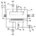
図1に本実施形態の半導体製造装置であるプラズマ処理装置の断面図を示す。図に示すように、ウェハwをプラズマ処理するための反応室11には、上部電極12と、これと対向配置される下部電極13が設置されている。(Embodiment 1)
FIG. 1 shows a cross-sectional view of a plasma processing apparatus which is a semiconductor manufacturing apparatus of the present embodiment. As shown in the figure, an
反応室11は、気密性を有しており、真空ポンプなどと接続され、真空に排気することが可能な排気口14が設けられている。排気口14には、排気量調整バルブ15が接続されており、反応室11内を所定の圧力に制御することが可能となっている。 The
上部電極12は、反応室11の上蓋に支持される円盤状のシャワー電極であり、上方より所定のガス種、流量のプロセスガスが導入されるプロセスガス導入口16と、プロセスガス導入口16より接続され、下面まで貫通してウェハwの被処理面にプロセスガスを噴射するための微小孔17が設けられている。下部電極13は、反応室11下部より支柱18により支持され、上面にウェハwが載置されるサセプタ19を有している。サセプタ19内には、サセプタ温度を一定に保つために冷却材を循環させるための冷却パイプ(図示せず)と抵抗加熱ヒータなどのヒータ20が内蔵されている。支柱18には上下駆動機構(図示せず)が設けられており、サセプタ19を昇降することにより上部電極12、下部電極13間の距離を変動させることが可能となっている。 The
これら上部電極12、下部電極13には、それぞれ上部電極12、下部電極13間に高周波電圧を印加するための高周波電源21、22が接続されるが、バイアスが印加されないプロセスでは、下部電極13は接地される。 The
反応室11の外側面には、上部電極12、下部電極13間の上部電極12側に、ウェハw面と離間して磁場を印加するための2段の電磁石23、24が設けられている。電磁石23、24には、例えばダイポールリングマグネットなど、水平磁場を発生することが可能なものが用いられる。そして、それぞれウェハwの被処理面に平行な磁場を発生させるとともに、磁場印加タイミングおよび強度を制御することが可能な制御機構を備えた電磁石電源25、26が設けられている。 On the outer surface of the
このようなプラズマ処理装置を用いて、例えば以下のようにプラズマによる処理が行われる。ここでは、メッキ法などによりCuダマシン配線が形成され、表面をCMP(Chemical Mechanical Polishing)法により平坦化されたSiウェハ上に、SiCNH組成を有する低誘電率膜(以下SiCNH膜と記す)をプラズマCVD法により堆積させる工程に適用した場合について説明する。 Using such a plasma processing apparatus, plasma processing is performed as follows, for example. Here, a Cu damascene wiring is formed by plating or the like, and a low dielectric constant film (hereinafter referred to as SiCNH film) having a SiCNH composition is formed on a Si wafer whose surface is planarized by a CMP (Chemical Mechanical Polishing) method. The case where it applies to the process deposited by CVD method is demonstrated.
成膜にあたり、ウェハの前処理としてプラズマエッチング処理を行う。Cuダマシン配線の表面には酸化物(CuOx)が存在するため、成膜前にこれを除去し、配線信頼性の劣化を防ぐためである。 In film formation, plasma etching is performed as a pretreatment of the wafer. This is because oxide (CuOx) is present on the surface of the Cu damascene wiring, so that it is removed before film formation to prevent deterioration of wiring reliability.
そこで、先ず、搬送室(図示せず)および反応室11内を、排気口14より真空排気し、ウェハwを搬送室(図示せず)より反応室11に搬送して、サセプタ19上に載置する。次いで、プラズマ処理が行われる温度、例えば350℃となるように、ヒータ20により加熱する。そして、例えばCuダマシン配線表面の酸化物を除去するためのNH3ガスが500sccm、これを希釈するためのN2ガスが10000sccmとなるように流量制御されたプロセスガスを、プロセスガス導入口16より導入し、微小孔17よりウェハw上に噴射する。Therefore, first, the inside of the transfer chamber (not shown) and the
このとき、反応室11内の圧力は、排気量調整バルブ15により、5Torrとなるように自動調圧される。そして、上部電極12と下部電極13の電極間距離が例えば30mmとなるように、支柱18によりサセプタ19を昇降させる。 At this time, the pressure in the
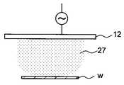
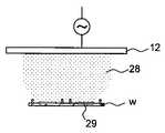
このような状態で、高周波電源21より上部電極12に例えば13.56MHzの高周波電圧を、下部電極13は接地し、500Wで放電を行う。このような高周波を印加すると、特に放電開始時(プラズマイグナイト時)は、ガスフロー中にプラズマが形成されるため、分子であったガスの乖離により体積膨張を生じ、一時的に反応室11内の圧力が増加する。そこで、圧力増加を補正するために、排気量調整バルブ15により排気量が自動的に調整されるが、このとき圧力変動が生じるため、図2に模式図を示すように、プラズマ27が不安定になり、ウェハw上のプラズマが不均一になる。この状態でプラズマ処理を行うと、図3に模式図を示すように、プラズマ28の不均一よりウェハw上にチャージアップ29が形成され、プラズマダメージを生じさせる。また、プラズマがウェハw上で均一でないことにより、チャージアップの不均一も生じる。それが加速要因となり、プラズマダメージが発生しやすくなる。 In such a state, a high frequency voltage of, for example, 13.56 MHz is applied from the high
そこで、例えば放電を行う5秒前に、それぞれ電磁石電源25、26より電磁石23、24に電流を流し、上段の電磁石23より、磁場200Gauss、下段の電磁石24より磁場100Gaussを発生させる。そして、磁場が発生した状態で、放電を開始することにより、図4に模式図を示すように、放電開始時にプラズマ30を上部電極12側に集中させる。 Therefore, for example, five seconds before discharging, currents are supplied from the
このように、磁場が発生した状態で放電を開始し、例えば3秒経過して上部電極12側でプラズマが安定化した状態で、それぞれ電磁石電源25、26からの電磁石23、24への電流を止め、磁場を除去する。これにより、上部電極12側に集中されていたプラズマ30が、図5に模式図を示すように、ウェハw上にプラズマ31が均一に暴露される。このとき、磁場の除去を段階的に1/2、1/3とすることで、さらにプラズマ31を均一に暴露することも可能である。具体的には、電磁石23は、例えば一秒毎に200Gauss、100Gauss、50Gaussとし、電磁石24は、例えば一秒毎に100Gauss、50Gauss、25Gaussとする。 In this way, the discharge is started in the state where the magnetic field is generated, and for example, the current from the
磁場を除いた後、ウェハwに対して例えば30秒間プラズマ処理を行うことにより、Cuダマシン配線上のCuOxが除去される。そして、同様に、それぞれ電磁石電源25、26より電磁石23、24に電流を流し、上段の電磁石23に、磁場200Gauss、下段の電磁石24に磁場100Gaussを発生させ、磁場が発生した状態で、高周波電圧を止め、放電を停止する。放電停止時には、ガスの乖離が止まるため、一時的に圧力が減少し、圧力変動が生じるため、プラズマが不安定になるが、放電停止時にプラズマを上部電極12側に集中させる。 After removing the magnetic field, the wafer w is subjected to plasma treatment for 30 seconds, for example, to remove CuOx on the Cu damascene wiring. Similarly, a current is supplied to the
そして、それぞれ電磁石電源25、26からの電磁石23、24への電流を止め、磁場を除去した後、プロセスガス導入口16からのNH3ガス、N2ガスの導入を停止し、排気量調整バルブ15を開いて排気口14より真空排気することにより、反応室11内のガスを除去する。And after stopping the electric current to the
次いで、CuOxが除去され清浄化されたCuダマシン配線上に、プラズマCVDによりSiCNH膜を成膜するために、今度はプロセスガスを成膜ガスに替えてプロセスガス導入口16より反応室11内に導入する。例えば、TMS(トリメチルシラン)ガスが400sccm、NH3ガスが800sccm、Heガスが2000sccmとなるように流量制御されたプロセスガスを、プロセスガス導入口16より導入し、微小孔17よりウェハw上に噴射する。このときウェハwは、350℃となるように、ヒータ20により加熱制御を行う。 Next, in order to form a SiCNH film by plasma CVD on the Cu damascene wiring from which CuOx has been removed and cleaned, this time, the process gas is changed to the film formation gas and the reaction gas is introduced into the
このとき、CuOx除去の際と同様に、反応室11内の圧力は、排気量調整バルブ15により、5Torrとなるように自動調圧される。そして、上部電極12と下部電極13の電極間距離が30mmとなるように、支柱18によりサセプタ19を昇降させる。 At this time, as in the case of removing CuOx, the pressure in the
このような状態で、高周波電源21より上部電極12に例えば13.56MHzの高周波電圧を印加し、下部電極13は接地し、今度は1000Wで放電を行う。そして、CuOx除去の際と同様に、例えば放電を行う5秒前に、それぞれ電磁石電源25、26より電磁石23、24に電流を流し、上段の電磁石23より、磁場200Gauss、下段の電磁石24より磁場100Gaussを発生させる。そして、磁場が発生した状態で、放電を開始することにより、放電開始時にプラズマを上部電極12側に集中させる。 In such a state, a high frequency voltage of 13.56 MHz, for example, is applied from the high
このように、磁場が発生した状態で放電を開始し、成膜される堆積膜(SiCNH膜)の膜質変動を抑えるために、例えば1秒経過して上部電極12側でプラズマが安定化した状態で、それぞれ電磁石電源25、26からの電磁石23、24への電流を止め、磁場を除去する。これにより、CuOx除去の際と同様に、上部電極12側に集中されていたプラズマが、ウェハw上に均一に暴露される。 Thus, in order to suppress the film quality fluctuation of the deposited film (SiCNH film) to be formed by starting discharge in a state where a magnetic field is generated, for example, a state in which the plasma is stabilized on the
磁場を除いた後、ウェハwに対して、例えば20秒間プラズマ処理を行うことにより、例えば50nmのSiCNH膜が成膜される。そして、同様に、それぞれ電磁石電源25、26より電磁石23、24に電流を流し、上段の電磁石23より、磁場200Gauss、下段の電磁石24より磁場100Gaussを発生させ、磁場が発生した状態で、高周波電圧を止め、放電を停止する。放電停止時には、ガスの乖離が止まるため、一時的に圧力が減少し、圧力変動が生じるため、プラズマが不安定になるが、放電停止時にプラズマを上部電極12側に集中させる。そして、それぞれ電磁石電源25、26からの電磁石23、24への電流を止め、磁場を除去した後、プロセスガス導入口16からのTMS(トリメチルシラン)ガス、NH3ガスが、Heガスの導入を停止し、排気量調整バルブ15を開いて排気口14より真空排気することにより、反応室11内のガスを除去する。 After removing the magnetic field, for example, a plasma treatment is performed on the wafer w for 20 seconds to form, for example, a 50 nm SiCNH film. Similarly, a current is supplied to the
このようにして、CuOxのプラズマエッチングによる除去、およびSiCNH膜のプラズマCVDによる成膜において、放電開始時、放電終了時において、ウェハ上にプラズマ不均一を形成することなく、プラズマ処理を行うことが可能となる。特に、放電開始時においては、プラズマ放電の基点が存在し、プラズマの不均一が生じやすくなるため、より効果的である。 In this way, in the removal by plasma etching of CuOx and the film formation of the SiCNH film by plasma CVD, plasma treatment can be performed at the start of discharge and at the end of discharge without forming plasma non-uniformity on the wafer. It becomes possible. In particular, at the start of discharge, the base point of plasma discharge exists, and plasma non-uniformity is likely to occur, which is more effective.
ここでは、高周波電源の周波数を13.56MHzとしたが、近年、膜質向上のため、より高周波(例えば60MHz)が利用されることがある。また、下部電極には、バイアスコントロールとして高周波が印加させる場合もある。この場合、よりプラズマの不均一が発生しやすくなり、プラズマダメージが起こりやすくなる。しかしながら、本実施形態によれば、膜質向上のために印加周波数を増大させても、プラズマ不均一によるデバイスダメージを抑制することができる。従って、形成されるトランジスタの性能不良や、製品歩留りの劣化を抑えることが可能となる。 Here, the frequency of the high-frequency power source is set to 13.56 MHz, but in recent years, a higher frequency (for example, 60 MHz) may be used to improve the film quality. In addition, a high frequency may be applied to the lower electrode as a bias control. In this case, plasma non-uniformity is more likely to occur, and plasma damage is likely to occur. However, according to the present embodiment, device damage due to plasma non-uniformity can be suppressed even when the applied frequency is increased to improve the film quality. Accordingly, it is possible to suppress poor performance of the formed transistor and deterioration of product yield.
また、例えば、ここで形成されたSiCNH膜は、低誘電率膜として用いられるが、デバイスダメージを生じることなく膜質を向上させることが可能であるため、配線間容量の低減など、デバイス性能の向上を図ることが可能となる。さらに、プロセス上も、Cuダマシン配線を形成する際に用いられるCuブロック膜、エッチングストッパー膜としても機能するものであるため、膜質の向上により、プロセスの安定化、歩留りの向上を図ることが可能となる。 In addition, for example, the SiCNH film formed here is used as a low dielectric constant film, but it is possible to improve the film quality without causing device damage. Can be achieved. Furthermore, since it functions as a Cu block film and an etching stopper film used when forming Cu damascene wiring, it is possible to stabilize the process and improve the yield by improving the film quality. It becomes.
また、プラズマが安定化された後、それぞれ電磁石電源25、26からの電磁石23、24への電流を止め、磁場を除去することにより、磁場によりプラズマの挙動が抑制されることがないため、メインプロセスへの磁場の影響を抑えることが可能となる。磁場を引き続き印加すると、例えば、CVD膜がウェハw上ではなく、上部電極周辺に形成されてしまい、ダストの発生要因となってしまう。さらに、成膜時間中、磁場の方向が一定で継続されると、磁場方向によりプラズマ高密度部分が発生し、成膜膜質の面内依存が顕著になってしまう。従って、プラズマ安定後の磁場除去により、品質の安定、歩留りの向上を図ることが可能となる。 Further, after the plasma is stabilized, the current to the
さらに、プラズマ処理装置においても、プラズマ不均一によるアーキングを抑制することができるため、プラズマ処理装置の劣化、メンテナンスコストを抑え、生産性を向上させることが可能となる。 Furthermore, since arcing due to plasma non-uniformity can also be suppressed in the plasma processing apparatus, it is possible to suppress degradation and maintenance costs of the plasma processing apparatus and improve productivity.
(実施形態2)
本実施形態は、実施形態1と同様に図1に示したプラズマ処理装置を用いてSiCNH膜を形成するが、成膜中に膜質、具体的には膜組成を変える点で異なっている。(Embodiment 2)
This embodiment forms a SiCNH film using the plasma processing apparatus shown in FIG. 1 as in the first embodiment, but differs in that the film quality, specifically the film composition, is changed during the film formation.
実施形態1と同様に、CuOxが除去され清浄化されたCuダマシン配線上に、プラズマCVDによりSiCNH膜を成膜する。例えば、実施形態1と同様に、TMS(トリメチルシラン)ガスが400sccm、NH3ガスが800sccm、Heガスが2000sccmとなるように流量制御されたプロセスガスを、プロセスガス導入口16より導入し、微小孔17よりウェハw上に噴射する。 As in the first embodiment, a SiCNH film is formed by plasma CVD on the Cu damascene wiring from which CuOx has been removed and cleaned. For example, as in the first embodiment, a process gas whose flow rate is controlled so that TMS (trimethylsilane) gas is 400 sccm, NH 3 gas is 800 sccm, and He gas is 2000 sccm is introduced from the
このとき、実施形態1と同様に、反応室11内の圧力を、5Torrとなるように自動調圧するとともに、上部電極12と下部電極13の電極間距離を例えば30mmとする。 At this time, as in the first embodiment, the pressure in the
このような状態で、実施形態1と同様に、高周波電源21より上部電極12に例えば13.56MHzの高周波電圧を印加し、下部電極13を接地し、1000Wで放電を行う。そして、例えば放電を行う5秒前に、それぞれ電磁石電源25、26より電磁石23、24に電流を流し、上段の電磁石23より、磁場200Gauss、下段の電磁石24より磁場100Gaussを発生させる。そして、磁場が発生した状態で、放電を開始することにより、放電開始時にプラズマを上部電極12側に集中させる。 In this state, as in the first embodiment, a high frequency voltage of, for example, 13.56 MHz is applied from the high
このように、磁場が発生した状態で放電を開始し、成膜される堆積膜(SiCNH膜)の膜質変動を抑えるために、例えば1秒経過して上部電極12側でプラズマが安定化した状態で、それぞれ電磁石電源25、26からの電磁石23、24への電流を止め、磁場を除去する。これにより、実施形態1と同様に、上部電極12側に集中されていたプラズマが、ウェハw上に均一に暴露される。 Thus, in order to suppress the film quality fluctuation of the deposited film (SiCNH film) to be formed by starting discharge in a state where a magnetic field is generated, for example, a state in which the plasma is stabilized on the
磁場を除去した後、ウェハwに対して、例えば20秒間プラズマ処理を行うことにより、例えば50nmのSiCNH膜が成膜される。 After removing the magnetic field, for example, a plasma treatment is performed on the wafer w for 20 seconds, for example, thereby forming a SiCNH film of 50 nm, for example.
次いで、それぞれ電磁石電源25、26より電磁石23、24に電流を流し、上段の電磁石23より、磁場200Gauss、下段の電磁石24より磁場100Gaussを発生させ、磁場が発生した状態で、例えば、DMPS(ジメチルフェニルシラン)ガスが1000mg/min、キャリアガスHeが2000sccm、Heガスが1000sccmとなるように流量制御されたプロセスガスを変動させ、プロセスガス導入口16より導入し、微小孔17よりウェハw上に噴射する。 Next, a current is supplied to the
このとき、同様に、反応室11内の圧力を、5Torrとなるように自動調圧するとともに、上部電極12と下部電極13の電極間距離を20mmとする。 At this time, similarly, the pressure in the
このような状態で、同様に高周波電源21より上部電極12に例えば13.56MHzの高周波電圧を印加し、下部電極13を接地し、今度は500Wで放電を行う。そして、1秒ほど経過し、プラズマ放電が安定したところで、それぞれ電磁石電源25、26からの電磁石23、24への電流を止め、磁場を除去する。 In such a state, a high-frequency voltage of 13.56 MHz, for example, is applied from the high-
磁場を除去した後、ウェハwに対して、例えば20秒間プラズマ処理を行うことにより、例えば下層のSiCH膜と膜質の異なるSiCH膜が50nm成膜される。そして、同様に、それぞれ電磁石電源25、26より電磁石23、24に電流を流し、上段の電磁石23に、磁場200Gauss、下段の電磁石24に磁場100Gaussを発生させ、磁場が発生した状態で、高周波電圧を止め、放電を停止した後、それぞれ電磁石電源25、26からの電磁石23、24への電流を止め、磁場を除去する。そして、プロセスガス導入口16からのガスの導入を停止し、排気量調整バルブ15を開いて排気口14より真空排気することにより、反応室11内のガスを除去する。このようにして、SiCNH/SiCH膜の積層構造が形成される。 After removing the magnetic field, for example, a plasma treatment is performed on the wafer w for 20 seconds, for example, to form a 50 nm SiCH film having a film quality different from that of the lower SiCH film. Similarly, a current is supplied to the
本実施形態において、成膜中に膜質を変動させる場合においても、プロセスガスなどの条件の変動により、プラズマ不均一が生じるが、実施形態1と同様に、ウェハ上にプラズマ不均一を形成することなく、プラズマ処理を行うことが可能となるなど、実施形態1と同様の効果を得ることができる。 In this embodiment, even when the film quality is changed during film formation, plasma non-uniformity occurs due to changes in conditions such as process gas. However, as in the first embodiment, plasma non-uniformity is formed on the wafer. However, it is possible to obtain the same effects as in the first embodiment, such as enabling plasma processing.
さらに、磁場が発生した状態で放電を開始し、プラズマが安定した状態で磁場を除去するため、新たに成膜される堆積膜(SiCH膜)の膜質変動を抑えることが可能となる。 Furthermore, since the discharge is started in the state where the magnetic field is generated and the magnetic field is removed in the state where the plasma is stable, it is possible to suppress the film quality fluctuation of the newly deposited film (SiCH film).
また、本実施形態において、SiCNH/SiCH膜の積層構造を形成しているが、一般に、SiCH膜はSiCNH膜に比べ、Cuブロック性能、エッチングストッパー性能は低いが、誘電率の低減を図ることができるため、多層配線の絶縁膜形成においては魅力的である。本実施形態において、このようなSiCNH/SiCH膜の積層構造をプラズマダメージなく、形成することが可能となる。 In the present embodiment, a SiCNH / SiCH film laminated structure is formed. In general, the SiCH film has lower Cu block performance and etching stopper performance than the SiCNH film, but the dielectric constant can be reduced. Therefore, it is attractive in forming an insulating film for multilayer wiring. In the present embodiment, it is possible to form such a laminated structure of SiCNH / SiCH films without plasma damage.
これら実施形態において、磁場を印加する時間、磁場の印加位置、磁場強度を所定の値としたが、例えば所定の条件で処理されたウェハにおける酸化膜などの劣化、破壊などのダメージなどを評価することにより、適宜最適化することができる。 In these embodiments, the magnetic field application time, the magnetic field application position, and the magnetic field strength are set to predetermined values. For example, evaluation is made on damage such as deterioration or destruction of an oxide film on a wafer processed under predetermined conditions. Therefore, it can be optimized as appropriate.
また、これら実施形態において、磁場を印加するための手段として、ダイポールリングマグネットを用いたが、特に限定されるものではなく、リング状のものであっても、複数の電磁石から構成されていてもよい。また、磁場はウェハwの被処理面から離間するように印加されていればよく、上部電極と下部電極の間に印加されることが好ましい。さらに、上下電極間距離の1/2より上部電極側に印加されることがより好ましい。 In these embodiments, a dipole ring magnet is used as a means for applying a magnetic field, but it is not particularly limited, and it may be a ring-shaped one or a plurality of electromagnets. Good. Moreover, the magnetic field should just be applied so that it may space apart from the to-be-processed surface of the wafer w, and it is preferable to apply between an upper electrode and a lower electrode. Furthermore, it is more preferable that the voltage be applied to the upper electrode side from 1/2 of the distance between the upper and lower electrodes.
また、磁場の向きは、ウェハwの被処理面と平行であることが好ましいが、必ずしも一軸方向に形成されている必要はない。さらに、磁場の向きが処理中に変動しても、同様の効果を得ることが可能である。 The direction of the magnetic field is preferably parallel to the surface to be processed of the wafer w, but it is not necessarily formed in a uniaxial direction. Furthermore, the same effect can be obtained even if the direction of the magnetic field fluctuates during processing.
尚、本発明は、上述した実施形態に限定されるものではない。その他要旨を逸脱しない範囲で種々変形して実施することができる。 In addition, this invention is not limited to embodiment mentioned above. Various other modifications can be made without departing from the scope of the invention.
w…ウェハ、11…反応室、12…上部電極、13…下部電極、14…排気口、15…排気量調整バルブ、16…プロセスガス導入口、17…微小孔、18…支柱、19…サセプタ、20…ヒータ、21、22…高周波電源、23、24…電磁石、25、26…電磁石電源、27、28、30、31…プラズマ、29…チャージアップ。 w ... wafer, 11 ... reaction chamber, 12 ... upper electrode, 13 ... lower electrode, 14 ... exhaust port, 15 ... displacement valve, 16 ... process gas inlet, 17 ... micro hole, 18 ... support, 19 ... susceptor , 20 ... heater, 21, 22 ... high frequency power supply, 23, 24 ... electromagnet, 25, 26 ... electromagnet power supply, 27, 28, 30, 31 ... plasma, 29 ... charge up.
Claims (5)
Translated fromJapanese前記反応室内にプロセスガスを導入し、
前記ウェハの被処理面と離間するように磁場を印加し、
前記下部電極と、前記下部電極と対向配置された上部電極間に高周波電圧を印加してプラズマを発生させ、
前記プラズマが安定化した後、前記磁場を除去し、
前記ウェハをプラズマ処理することを特徴とする半導体製造方法。Place the wafer on the lower electrode provided in the reaction chamber,
Introducing process gas into the reaction chamber;
Applying a magnetic field so as to be separated from the surface to be processed of the wafer;
A plasma is generated by applying a high frequency voltage between the lower electrode and the upper electrode disposed opposite to the lower electrode,
After the plasma is stabilized, the magnetic field is removed,
A semiconductor manufacturing method, wherein the wafer is plasma-processed.
前記磁場を印加し、
前記高周波電圧の印加を止めた後、前記磁場を除去することを特徴とする請求項1に記載の半導体製造方法。After the wafer is plasma treated,
Applying the magnetic field;
The semiconductor manufacturing method according to claim 1, wherein the magnetic field is removed after the application of the high-frequency voltage is stopped.
プロセス条件を変動させ、
前記磁場を除去することを特徴とする請求項1または請求項2に記載の半導体製造方法。Applying the magnetic field;
Fluctuate process conditions,
The semiconductor manufacturing method according to claim 1, wherein the magnetic field is removed.
それぞれ前記反応室内に配置され、プロセスガス導入口を有する上部電極、および前記上部電極と対向配置され、ウェハを載置するための載置面を有する下部電極と、
前記上部電極および前記下部電極間に高周波電圧を印加するための高周波電源と、
前記上部電極および前記下部電極間の前記上部電極側に、前記ウェハの被処理面と離間するように磁場を印加するための磁場印加機構と、
前記上部電極および前記下部電極の間に前記高周波電圧が印加される前に前記磁場を印加し、前記上部電極および前記下部電極の間に前記高周波電圧を印加することにより発生したプラズマが安定化した後に前記磁場を除去するように、前記磁場印加機構を制御するための磁場制御機構と、
を備えることを特徴とする半導体製造装置。A reaction chamber for plasma processing the wafer;
An upper electrode disposed in the reaction chamber and having a process gas inlet, and a lower electrode disposed opposite to the upper electrode and having a mounting surface for mounting a wafer;
A high frequency power source for applying a high frequency voltage between the upper electrodeand the lower electrode;
A magnetic field application mechanism for applying a magnetic field to the upper electrode side between the upper electrodeand the lower electrode so as to be separated from the processing surface of the wafer;
The magnetic field is applied before the high-frequency voltage is applied between the upper electrode and the lower electrode, and the generated plasma is stabilized by applying the high-frequency voltage between the upper electrode and the lower electrode. A magnetic field control mechanism for controlling themagnetic field application mechanism so as to remove the magnetic field later;
A semiconductor manufacturing apparatus comprising:
Priority Applications (2)
| Application Number | Priority Date | Filing Date | Title |
|---|---|---|---|
| JP2007318267AJP4896861B2 (en) | 2007-12-10 | 2007-12-10 | Semiconductor manufacturing method and semiconductor manufacturing apparatus |
| US12/331,199US20090156002A1 (en) | 2007-12-10 | 2008-12-09 | Manufacturing method for semiconductor device and manufacturing apparatus for semiconductor device |
Applications Claiming Priority (1)
| Application Number | Priority Date | Filing Date | Title |
|---|---|---|---|
| JP2007318267AJP4896861B2 (en) | 2007-12-10 | 2007-12-10 | Semiconductor manufacturing method and semiconductor manufacturing apparatus |
Publications (2)
| Publication Number | Publication Date |
|---|---|
| JP2009141251A JP2009141251A (en) | 2009-06-25 |
| JP4896861B2true JP4896861B2 (en) | 2012-03-14 |
Family
ID=40753835
Family Applications (1)
| Application Number | Title | Priority Date | Filing Date |
|---|---|---|---|
| JP2007318267AExpired - Fee RelatedJP4896861B2 (en) | 2007-12-10 | 2007-12-10 | Semiconductor manufacturing method and semiconductor manufacturing apparatus |
Country Status (2)
| Country | Link |
|---|---|
| US (1) | US20090156002A1 (en) |
| JP (1) | JP4896861B2 (en) |
Families Citing this family (2)
| Publication number | Priority date | Publication date | Assignee | Title |
|---|---|---|---|---|
| WO2019087691A1 (en)* | 2017-10-31 | 2019-05-09 | パナソニックIpマネジメント株式会社 | Structure and method for producing same |
| CN112359335B (en) | 2020-10-23 | 2023-01-17 | 北京北方华创微电子装备有限公司 | Semiconductor processing equipment and process chamber thereof |
Family Cites Families (15)
| Publication number | Priority date | Publication date | Assignee | Title |
|---|---|---|---|---|
| JPS62205618A (en)* | 1986-03-06 | 1987-09-10 | Ulvac Corp | Plasma cvd unit |
| JP2732294B2 (en)* | 1989-04-20 | 1998-03-25 | 三洋電機株式会社 | Thin film formation method |
| JPH06177051A (en)* | 1992-12-10 | 1994-06-24 | Tdk Corp | Cvd device |
| US5456796A (en)* | 1993-06-02 | 1995-10-10 | Applied Materials, Inc. | Control of particle generation within a reaction chamber |
| JPH10172793A (en)* | 1996-12-17 | 1998-06-26 | Mitsubishi Heavy Ind Ltd | Plasma generator |
| US6028286A (en)* | 1998-12-30 | 2000-02-22 | Lam Research Corporation | Method for igniting a plasma inside a plasma processing reactor |
| JP4285853B2 (en)* | 1999-09-08 | 2009-06-24 | 東京エレクトロン株式会社 | Processing method |
| JP4437351B2 (en)* | 2000-01-14 | 2010-03-24 | キヤノンアネルバ株式会社 | Plasma etching equipment |
| JP5010781B2 (en)* | 2001-03-28 | 2012-08-29 | 忠弘 大見 | Plasma processing equipment |
| JP2002353200A (en)* | 2001-05-28 | 2002-12-06 | Hitachi Ltd | Method for manufacturing semiconductor device |
| JP4009087B2 (en)* | 2001-07-06 | 2007-11-14 | アプライド マテリアルズ インコーポレイテッド | Magnetic generator in semiconductor manufacturing apparatus, semiconductor manufacturing apparatus, and magnetic field intensity control method |
| US7374636B2 (en)* | 2001-07-06 | 2008-05-20 | Applied Materials, Inc. | Method and apparatus for providing uniform plasma in a magnetic field enhanced plasma reactor |
| US6521082B1 (en)* | 2002-04-16 | 2003-02-18 | Applied Materials Inc. | Magnetically enhanced plasma apparatus and method with enhanced plasma uniformity and enhanced ion energy control |
| JP4865352B2 (en)* | 2006-02-17 | 2012-02-01 | 三菱重工業株式会社 | Plasma processing apparatus and plasma processing method |
| JP4801522B2 (en)* | 2006-07-21 | 2011-10-26 | 株式会社日立ハイテクノロジーズ | Semiconductor manufacturing apparatus and plasma processing method |
- 2007
- 2007-12-10JPJP2007318267Apatent/JP4896861B2/ennot_activeExpired - Fee Related
- 2008
- 2008-12-09USUS12/331,199patent/US20090156002A1/ennot_activeAbandoned
Also Published As
| Publication number | Publication date |
|---|---|
| US20090156002A1 (en) | 2009-06-18 |
| JP2009141251A (en) | 2009-06-25 |
Similar Documents
| Publication | Publication Date | Title |
|---|---|---|
| US10304668B2 (en) | Localized process control using a plasma system | |
| US8440050B2 (en) | Plasma processing apparatus and method, and storage medium | |
| US11081318B2 (en) | Geometrically selective deposition of dielectric films utilizing low frequency bias | |
| US20050039854A1 (en) | Plasma etching method and plasma etching unit | |
| US11315769B2 (en) | Plasma source for rotating susceptor | |
| US11315763B2 (en) | Shaped electrodes for improved plasma exposure from vertical plasma source | |
| CN111095498B (en) | Mounting table, substrate processing apparatus, and edge ring | |
| TWI811432B (en) | Etching method and plasma treatment device | |
| US10577689B2 (en) | Sputtering showerhead | |
| KR20150024277A (en) | Semiconductor device manufacturing method | |
| JP7618579B2 (en) | Electrostatic Chuck Process | |
| JP4642809B2 (en) | Plasma processing method and plasma processing apparatus | |
| US11705312B2 (en) | Vertically adjustable plasma source | |
| KR20170053134A (en) | Method of processing workpiece | |
| US6811831B1 (en) | Method for depositing silicon nitride | |
| JP4896861B2 (en) | Semiconductor manufacturing method and semiconductor manufacturing apparatus | |
| US20020192984A1 (en) | Method for manufacturing semiconductor device, method for processing substrate, and substrate processing apparatus | |
| JPH10237639A (en) | Sputtering equipment for producing barrier films for integrated circuits | |
| TW202329191A (en) | Transformer coupled plasma source design for thin dielectric film deposition | |
| KR20230024701A (en) | Method for treating substrate | |
| KR20240019752A (en) | Wafer processing method |
Legal Events
| Date | Code | Title | Description |
|---|---|---|---|
| A621 | Written request for application examination | Free format text:JAPANESE INTERMEDIATE CODE: A621 Effective date:20100217 | |
| A977 | Report on retrieval | Free format text:JAPANESE INTERMEDIATE CODE: A971007 Effective date:20110826 | |
| A131 | Notification of reasons for refusal | Free format text:JAPANESE INTERMEDIATE CODE: A131 Effective date:20110906 | |
| A521 | Request for written amendment filed | Free format text:JAPANESE INTERMEDIATE CODE: A523 Effective date:20111027 | |
| TRDD | Decision of grant or rejection written | ||
| A01 | Written decision to grant a patent or to grant a registration (utility model) | Free format text:JAPANESE INTERMEDIATE CODE: A01 Effective date:20111129 | |
| A01 | Written decision to grant a patent or to grant a registration (utility model) | Free format text:JAPANESE INTERMEDIATE CODE: A01 | |
| A61 | First payment of annual fees (during grant procedure) | Free format text:JAPANESE INTERMEDIATE CODE: A61 Effective date:20111221 | |
| FPAY | Renewal fee payment (event date is renewal date of database) | Free format text:PAYMENT UNTIL: 20150106 Year of fee payment:3 | |
| LAPS | Cancellation because of no payment of annual fees |