JP4889268B2 - EEPROM and driving method of EEPROM - Google Patents
EEPROM and driving method of EEPROMDownload PDFInfo
- Publication number
- JP4889268B2 JP4889268B2JP2005275356AJP2005275356AJP4889268B2JP 4889268 B2JP4889268 B2JP 4889268B2JP 2005275356 AJP2005275356 AJP 2005275356AJP 2005275356 AJP2005275356 AJP 2005275356AJP 4889268 B2JP4889268 B2JP 4889268B2
- Authority
- JP
- Japan
- Prior art keywords
- diffusion region
- well
- oxide film
- mos transistor
- gate oxide
- Prior art date
- Legal status (The legal status is an assumption and is not a legal conclusion. Google has not performed a legal analysis and makes no representation as to the accuracy of the status listed.)
- Expired - Fee Related
Links
Images


Classifications
- G—PHYSICS
- G11—INFORMATION STORAGE
- G11C—STATIC STORES
- G11C16/00—Erasable programmable read-only memories
- G11C16/02—Erasable programmable read-only memories electrically programmable
- G11C16/04—Erasable programmable read-only memories electrically programmable using variable threshold transistors, e.g. FAMOS
- G11C16/0408—Erasable programmable read-only memories electrically programmable using variable threshold transistors, e.g. FAMOS comprising cells containing floating gate transistors
- G11C16/0425—Erasable programmable read-only memories electrically programmable using variable threshold transistors, e.g. FAMOS comprising cells containing floating gate transistors comprising cells containing a merged floating gate and select transistor
Landscapes
- Engineering & Computer Science (AREA)
- Microelectronics & Electronic Packaging (AREA)
- Non-Volatile Memory (AREA)
- Read Only Memory (AREA)
- Control Of Indicators Other Than Cathode Ray Tubes (AREA)
- Semiconductor Memories (AREA)
- Liquid Crystal Display Device Control (AREA)
Description
Translated fromJapanese本発明はEEPROM及びその駆動方法に関し、特に液晶ドライバICに混載されるEEPROM及びその駆動方法に関する。 The present invention relates to an EEPROM and a driving method thereof, and more particularly to an EEPROM embedded in a liquid crystal driver IC and a driving method thereof.
近年、これまで外付け用部品として使用してきたEEPROMを、実装時の部品点数の減少や液晶ドライバICの特性調整用途などで、ICそのものに内臓する要求が強まっている。 In recent years, there has been an increasing demand for incorporating EEPROM, which has been used as an external component so far, into the IC itself in order to reduce the number of components at the time of mounting or to adjust the characteristics of the liquid crystal driver IC.
液晶ドライバICに混載するEEPROMはその用途から、ビット数は数ビット〜数百ビットと少数ビットでよい、書換回数は数回でよい、データ保持信頼性は長期にわたって保証しなければならない、コスト増はできない、という特徴がある。そこで、面積的には不利であるが、既存のCMOSプロセスに対して少数の追加工程で作成でき、コスト的に有利な1層ポリ型のEEPROMが必要とされている。 The EEPROM embedded in the LCD driver IC can be used in a few bits, from a few bits to a few hundred bits, the number of rewrites may be several, the data retention reliability must be guaranteed over a long period, and the cost increases. There is a feature that can not. Therefore, there is a need for a single-layer poly-type EEPROM that is disadvantageous in terms of area, but can be formed with a small number of additional steps compared to an existing CMOS process, and is advantageous in terms of cost.
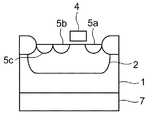
これまでの1層ポリ型のEEPROMは、例えば特許文献に記載されているように、図7の構成で形成される。このEEPROMはNchとPchのトランジスタのゲートポリ8を共通にして形成している。Nch型MOSトランジスタは拡散層2a、2b及びゲート電極3で構成される。Pch型MOSトランジスタは拡散層5a、5b及びゲート電極7で構成される。1はp型半導体基板、4はn型ウェル、6は拡散層、9、10、11は電源供給用の端子である。この二つのトランジスタは、それぞれデータリード用トランジスタとコントロールゲート用ウェル容量として用いる。また、データリード用トランジスのゲート容量よりコントロールゲート用ウェル容量のゲート容量を小さくしている。 図7ではNchトランジスタをデータリード用トランジスタ、Pchトランジスタをコントロールゲート用ウェル容量として形成している。 The conventional single-layer poly-type EEPROM is formed with the configuration shown in FIG. 7 as described in, for example, patent literature. This EEPROM is formed by sharing the gate poly 8 of the Nch and Pch transistors. The Nch type MOS transistor is composed of diffusion layers 2 a and 2 b and a
この特許文献に記載のEEPROMの動作条件を以下に記載する。 The operating conditions of the EEPROM described in this patent document are described below.
データ書き込み時はNchトランジスタのみでのFNトンネル電流又はホットキャリア注入でデータを書き込む。データ消去時はNchまたはPchトランジスタでのFNトンネル電流でデータを消去する。データリードはNchトランジスタで行う。そのデータリードの際にPchトランジスタ部には電圧+Vrを印加して、セルのゲート電圧を上げてデータのセンスを行う。 At the time of data writing, data is written by FN tunnel current or hot carrier injection using only the Nch transistor. When erasing data, the data is erased by the FN tunnel current in the Nch or Pch transistor. Data read is performed by Nch transistor. At the time of the data read, the voltage + Vr is applied to the Pch transistor portion to raise the cell gate voltage and sense the data.
従来技術のEEPROMはその構成上、2つのトランジスタを用いてはいても、一方はトランジスタ(データリード用)、もう一方は容量(コントロールゲート用)として動作する。リード時のセルの特性はデータリード用トランジスタの特性が支配的である為、セルの特性として重要なのはデータリード用トランジスタの方である。 Although the conventional EEPROM uses two transistors due to its configuration, one operates as a transistor (for data read) and the other as a capacitor (for control gate). Since the characteristics of the cell for data reading are dominated by the characteristics of the data reading transistor, the data reading transistor is more important as the characteristics of the cell.
しかし、従来技術ではデータの書き込みや消去の際にデータリード用トランジスタを用いている為、ホットキャリア注入やFNトンネル電流がデータリード用トランジスタ部のゲート酸化膜に大きなストレスを与えてしまう。それ故に、EEPROMセルのデータ保持信頼性に大きな悪影響を与える。 However, in the prior art, a data read transistor is used for writing or erasing data, so that hot carrier injection or FN tunnel current gives a large stress to the gate oxide film of the data read transistor portion. Therefore, the data retention reliability of the EEPROM cell is greatly adversely affected.
また、この影響を小さくする為、消去をコントロールゲート用ウェル容量で行うようにした場合、そちらのゲート酸化膜へストレスがかかることになる。EEPROMセルの特性の重要度から考えるとこの手法は有効であるが、従来技術のようにデータをリードする際に容量部に電圧をかけてしまうと、データリードするたびにゲート酸化膜に電界がかかることになり、これもセルのデータ保持信頼性に大きな悪影響を与える。 Further, in order to reduce this influence, when erasing is performed by the well capacity for the control gate, stress is applied to the gate oxide film. This method is effective in view of the importance of the characteristics of the EEPROM cell. However, if a voltage is applied to the capacitor when reading data as in the prior art, an electric field is applied to the gate oxide film every time data is read. As a result, this also has a great adverse effect on the data retention reliability of the cell.
データの書き込み及び消去をデータリード用トランジスタでは一切行わないことでセルのデータ保持信頼性向上を図る。更に、データリード時にゲート酸化膜に電界をかけないようにすることでセルのデータ保持信頼性向上を図る。 Data writing and erasing are not performed at all by the data read transistor, thereby improving the data retention reliability of the cell. Further, the data retention reliability of the cell is improved by not applying an electric field to the gate oxide film during data reading.
以上説明したように、本発明によれば、データの書き込み及び消去を、データリード用トランジスタを一切行わないで容量として機能するトランジスタで行うので、データリード用トランジスタ部のゲート酸化膜にストレスを与えない。したがって、本発明のEEPROMは、そのデータ保持信頼性を改善することができる。 As described above, according to the present invention, data writing and erasing are performed by a transistor functioning as a capacitor without performing any data reading transistor, so that stress is applied to the gate oxide film of the data reading transistor portion. Absent. Therefore, the EEPROM of the present invention can improve the data retention reliability.
本発明の前記ならびにその他の目的、特徴、及び効果をより明確にすべく、以下図面を用いて本発明の実施の形態につき詳述する。 In order to clarify the above and other objects, features, and effects of the present invention, embodiments of the present invention will be described in detail below with reference to the drawings.
図1は本発明のEEPROMの実施の形態の平面図である。図1は、EEPROMの1セルを示す図面である。図2は、図1の1A−1A'におけるデータリード用トランジスタの断面図である。図3は、図1の1B−1B'におけるコントロールゲート用ウェル容量の断面図である。 FIG. 1 is a plan view of an embodiment of the EEPROM of the present invention. FIG. 1 is a diagram showing one cell of an EEPROM. 2 is a cross-sectional view of the data read
本発明のEEPROMは、p型基板の電位から素子を分離させるNウェル1、コントロールゲート用ウェル容量を構成しているNウェル2、データリード用トランジスタを構成しているPウェル3、その二素子に共通で用いているポリシリコン4を備える。ポリシリコン4は、EEPROMセルのフローティングゲートとなる。本発明のEEPROMは、更に、コントロールゲート用ウェル容量を構成する拡散層5a〜5cを有し、夫々ドレイン用p+拡散層5a、ソース用p+拡散層5b、バックゲート用n+拡散層5cである。更に、本発明のEEPROMは、データリード用トランジスタを構成する拡散層6a〜6cを有し、夫々ドレイン用n+拡散層6a、ソース用n+拡散層6b、バックゲート用p+拡散層6cである。7はp型半導体基板である。図示はしていないがp型半導体基板7とポリシリコン4の間にはゲート酸化膜が形成されている。 The EEPROM of the present invention includes an
以下、本発明のEEPROMの動作方法について説明する。
[データ消去時]
図4にデータ消去動作時の電圧印加条件を示す。The operation method of the EEPROM of the present invention will be described below.
[When deleting data]
FIG. 4 shows voltage application conditions during the data erasing operation.
データリード用トランジスタを構成している拡散層6a〜6cは全て0[V]とする。コントロールゲート用ウェル容量を構成している拡散層5a〜5cは全て+VE[V]とする。このような電圧を印加することにより、コントロールゲート用ウェル容量のゲート酸化膜にFNトンネル電流を流し、フローティングゲート中に帯電されているエレクトロンを放出する。
[データ書き込み時]
図5にデータ書き込み動作時の電圧印加条件を示す。The
[When writing data]
FIG. 5 shows the voltage application conditions during the data write operation.
データリード用トランジスタを構成している拡散層6a〜6cは全て0[V]とする。コントロールゲート用ウェル容量を構成している拡散層5aを0[V]、拡散層5b、5cを+VW[V]とする。このような電圧を印加することにより、コントロールゲート用ウェル容量として用いているPchトランジスタがオンして、拡散層5aと拡散層5bの間で電流が流れる。それによりホットエレクトロンが生成され、フローティングゲート中にエレクトロンが帯電されデータがEEPROMに書き込まれる。 The
[データリード時]
図6にデータリード動作時の電圧印加条件を示す。[When reading data]
FIG. 6 shows voltage application conditions during the data read operation.
データリード用トランジスタを構成している拡散層6aは+Vr[V]、拡散層6b及び6cは0[V]とする。コントロールゲート用ウェル容量を構成している拡散層5a〜5cは全て0[V]とする。この状態でデータリードトランジスタがオンするかどうかでデータの有無を判断する。データが書き込まれている場合、フローティングゲートにはエレクトロンが過剰に存在するためオフ状態となる。データが消去されている場合、フローティングゲートはエレクトロンが欠乏した状態となるためオン状態となる。 The
以上のように、本発明のEEPROMは、データ書き込み及び消去時に電荷授受が行われる素子とデータリード時に動作させる素子を明確に分けている。これにより、データリード部トランジスタのゲート酸化膜の劣化を最小限に抑えることが可能であり、EEPROMセルとしてのデータ保持信頼性を向上することができる。更に、電荷授受を行ったコントロールゲート用ウェル容量部のゲート酸化膜に関しても、データリード時には電界がかからないように、0V固定としているため、セルのデータ保持信頼性向上が可能である。 As described above, the EEPROM of the present invention clearly separates an element that receives and transfers charges when writing and erasing data and an element that operates when reading data. Thereby, it is possible to minimize the deterioration of the gate oxide film of the data read portion transistor, and the data retention reliability as the EEPROM cell can be improved. Further, the gate oxide film of the well capacity portion for the control gate that has received and transferred the charge is fixed at 0 V so that no electric field is applied during data reading, so that the data retention reliability of the cell can be improved.
なお、本発明は上記各実施例に限定されず、本発明の技術思想の範囲内において、各実施例は適宜変更され得ることは明らかである。なお、本発明におけるEEPROM(Electronically Erasable and Programmable Read Only Memory )は、電気的に内容を書き換えることができるROMと定義される。 It should be noted that the present invention is not limited to the above-described embodiments, and it is obvious that the embodiments can be appropriately changed within the scope of the technical idea of the present invention. Note that an EEPROM (Electronically Erasable and Programmable Read Only Memory) in the present invention is defined as a ROM whose contents can be electrically rewritten.
1 基板分離用Nウェル
2 Nウェル
3 Pウェル
4 ポリシリコン(フローティングゲート)
5a p+拡散層ドレイン(コントロールゲート)
5b p+拡散層ソース(コントロールゲート)
5c n+拡散層バックゲート(コントロールゲート)
6a n+拡散層ドレイン(リードトランジスタ)
6b n+拡散層ソース(リードトランジスタ)
6c p+拡散層バックゲート(リードトランジスタ)
7 p型半導体基板
1 N-well for substrate separation
2 N well
3 P well 4 Polysilicon (floating gate)
5a p + diffusion layer drain (control gate)
5b p + diffusion layer source (control gate)
5c n + diffusion layer back gate (control gate)
6an + diffusion layer drain (read transistor)
6b n + diffusion layer source (read transistor)
6c p + diffusion layer back gate (read transistor)
7 p-type semiconductor substrate
Claims (2)
Translated fromJapanese前記第1MOSトランジスタと同じセルに形成された第2MOSトランジスタと
を具備し、
前記第1MOSトランジスタは、
第1導電型の第1ウェルと、
前記第1ウェルに形成された第2導電型の第1拡散領域と、
前記第1ウェルに形成された第2導電型の第2拡散領域と、
前記第1ウェルの上に形成された第1ゲート酸化膜と、
前記第1ゲート酸化膜の上に形成されたフローティングゲートと
を備え、
前記第2MOSトランジスタは、
第2導電型の第2ウェルと、
前記第2ウェルに形成された第1導電型の第3拡散領域と、
前記第2ウェルに形成された第1導電型の第4拡散領域と、
前記第2ウェルの上に形成された第2ゲート酸化膜と、
前記第1MOSトランジスタから延在する、前記第2ゲート酸化膜の上に形成された前記フローティングゲートと
を備え、
前記第1MOSトランジスタ及び前記第2MOSトランジスタは、
データ書き込み動作として、前記第1ウェルにホットエレクトロンが生成されるように、前記第1拡散領域に正の電圧が印加され、且つ、前記第2拡散領域、前記第3拡散領域、及び前記第4拡散領域に0Vが印加されると、前記第1ゲート酸化膜を介して前記第1ウェルから前記フローティングゲートへ電子を放出し、
データ読出し動作として、前記第3拡散領域に正の電圧が印加され、且つ、前記第1拡散領域、前記第2拡散領域、及び前記第4拡散領域に0Vが印加されると、前記フローティングゲートに帯電した電子に応じて前記第2MOSトランジスタがオン状態又はオフ状態となり、
データ消去動作として、前記第1ゲート酸化膜にトンネル電流が流れるように、前記第1拡散領域、及び前記第2拡散領域に正の電圧が印加され、且つ、前記第3拡散領域、及び前記第4拡散領域に0Vが印加されると、前記フローティングゲート中に帯電している電子を、前記第1ゲート酸化膜を介して前記第1ウェルへ放出する
EEPROM。A first MOS transistor;
A second MOS transistor formed in the same cell as the first MOS transistor,
The first MOS transistor is
A first well of a first conductivity type;
A first diffusion region of a second conductivity type formed in the first well;
A second conductivity type second diffusion region formed in the first well;
A first gate oxide film formed on the first well;
A floating gate formed on the first gate oxide film,
The second MOS transistor is
A second well of a second conductivity type;
A third diffusion region of the first conductivity type formed in the second well;
A fourth diffusion region of the first conductivity type formed in the second well;
A second gate oxide film formed on the second well;
The floating gate formed on the second gate oxide film extending from the first MOS transistor;
The first MOS transistor and the second MOS transistor are:
As a data write operation,so that hot electrons are generated in the first well, apositive voltage is applied to the first diffusion region and said second diffusionregion, before Symbol third diffusion region, and the first When 0V is applied to the four diffusion regions, electrons are emitted from the first well to the floating gate through the first gate oxide film,
As the data read operation, thepositive voltage to the third diffusion region is applied,and, before Symbol first diffusion region, said second diffusionregion, when 0V is applied to及 beauty said fourth diffusion region, said floating wherein the 2MOS transistor according charged electrons to gateRi Do turned on oroff,
As the data erasing operation, a positive voltage is applied to the first diffusion region and the second diffusion region so that a tunnel current flows through the first gate oxide film, and the third diffusion region and the second diffusion region 4. An EEPROM thatdischarges electrons charged in the floating gate to the first well through the first gate oxide film when 0V is applied to the four diffusion regions .
前記第1MOSトランジスタと同じセルに形成された第2MOSトランジスタと
を具備し、
前記第1MOSトランジスタは、
第1導電型の第1ウェルと、
前記第1ウェルに形成された第2導電型の第1拡散領域と、
前記第1ウェルに形成された第2導電型の第2拡散領域と、
前記第1ウェルの上に形成された第1ゲート酸化膜と、
前記第1ゲート酸化膜の上に形成されたフローティングゲートと
を備え、
前記第2MOSトランジスタは、
第2導電型の第2ウェルと、
前記第2ウェルに形成された第1導電型の第3拡散領域と、
前記第2ウェルに形成された第1導電型の第4拡散領域と、
前記第2ウェルの上に形成された第2ゲート酸化膜と、
前記第1MOSトランジスタから延在する、前記第2ゲート酸化膜の上に形成された前記フローティングゲートと
を備えるEEPROMの駆動方法であって、
前記第1拡散領域に印加される正の電圧と、前記第2拡散領域、前記第3拡散領域、及び前記第4拡散領域に印加される0Vとに基づいて、前記第1ウェルにホットエレクトロンを生成し、前記第1ゲート酸化膜を介して前記第1ウェルから前記フローティングゲートへ電子を放出するデータ書き込み動作と、
前記第3拡散領域に印加される正の電圧と、前記第1拡散領域、前記第2拡散領域、及び前記第4拡散領域に印加される0Vとに基づいて、前記フローティングゲートに帯電した電子に応じて前記第2MOSトランジスタがオン状態又はオフ状態となるデータ読出し動作と、
前記第1拡散領域、及び前記第2拡散領域に印加される正の電圧と、前記第3拡散領域、及び前記第4拡散領域に印加される0Vとに基づいて、前記第1ゲート酸化膜にトンネル電流を流し、前記フローティングゲート中に帯電している電子を、前記第1ゲート酸化膜を介して前記第1ウェルへ放出するデータ消去動作と
を具備する
EEPROMの駆動方法。A first MOS transistor;
A second MOS transistor formed in the same cell as the first MOS transistor,
The first MOS transistor is
A first well of a first conductivity type;
A first diffusion region of a second conductivity type formed in the first well;
A second conductivity type second diffusion region formed in the first well;
A first gate oxide film formed on the first well;
A floating gate formed on the first gate oxide film,
The second MOS transistor is
A second well of a second conductivity type;
A third diffusion region of the first conductivity type formed in the second well;
A fourth diffusion region of the first conductivity type formed in the second well;
A second gate oxide film formed on the second well;
An EEPROM driving method comprising: the floating gate formed on the second gate oxide film extending from the first MOS transistor;
Before Symbolpositive voltage Ru aremarked additionto the first diffusionregion, before Symbol second diffusionregion, before Symbol third diffusion region, andbased on the 0Vapplied to the fourth diffusionregion, the first wellData writing operationfor generating hot electrons in the first gate oxide film and emitting electrons from the first well to the floating gate through the first gate oxide film;
Before Symbol third diffusion regionto mark pressurized byRu positive voltage, before Symbol first diffusion region, said second diffusionregion,based on the 0Vapplied to及 beauty said fourth diffusion region, said floating gate Adata read operation in which the second MOS transistor is turned on or off according to charged electrons;
Based on a positive voltage applied to the first diffusion region and the second diffusion region, and 0V applied to the third diffusion region and the fourth diffusion region, the first gate oxide film A data erasing operation in which a tunnel current flows and electrons charged in the floating gate are discharged to the first well through the first gate oxide film;
A method for drivingan EEPROMcomprising :
Priority Applications (3)
| Application Number | Priority Date | Filing Date | Title |
|---|---|---|---|
| JP2005275356AJP4889268B2 (en) | 2005-09-22 | 2005-09-22 | EEPROM and driving method of EEPROM |
| US11/524,300US7489550B2 (en) | 2005-09-22 | 2006-09-21 | EEPROM and method of driving the same |
| CNB2006101540695ACN100552960C (en) | 2005-09-22 | 2006-09-22 | Eeprom and driving method thereof |
Applications Claiming Priority (1)
| Application Number | Priority Date | Filing Date | Title |
|---|---|---|---|
| JP2005275356AJP4889268B2 (en) | 2005-09-22 | 2005-09-22 | EEPROM and driving method of EEPROM |
Publications (2)
| Publication Number | Publication Date |
|---|---|
| JP2007088216A JP2007088216A (en) | 2007-04-05 |
| JP4889268B2true JP4889268B2 (en) | 2012-03-07 |
Family
ID=37883873
Family Applications (1)
| Application Number | Title | Priority Date | Filing Date |
|---|---|---|---|
| JP2005275356AExpired - Fee RelatedJP4889268B2 (en) | 2005-09-22 | 2005-09-22 | EEPROM and driving method of EEPROM |
Country Status (3)
| Country | Link |
|---|---|
| US (1) | US7489550B2 (en) |
| JP (1) | JP4889268B2 (en) |
| CN (1) | CN100552960C (en) |
Cited By (3)
| Publication number | Priority date | Publication date | Assignee | Title |
|---|---|---|---|---|
| US9393573B2 (en) | 2014-04-24 | 2016-07-19 | Separation Technologies Llc | Continuous belt for belt-type separator devices |
| US9764332B2 (en) | 2015-02-13 | 2017-09-19 | Separation Technologies Llc | Edge air nozzles for belt-type separator devices |
| US11998930B2 (en) | 2020-06-22 | 2024-06-04 | Separation Technologies Llc | Process for dry beneficiation of fine and very fine iron ore by size and electrostatic segregation |
Families Citing this family (7)
| Publication number | Priority date | Publication date | Assignee | Title |
|---|---|---|---|---|
| US7483310B1 (en)* | 2006-11-02 | 2009-01-27 | National Semiconductor Corporation | System and method for providing high endurance low cost CMOS compatible EEPROM devices |
| US7804714B1 (en) | 2007-02-21 | 2010-09-28 | National Semiconductor Corporation | System and method for providing an EPROM with different gate oxide thicknesses |
| US8067795B2 (en)* | 2007-03-12 | 2011-11-29 | Texas Instruments Incorporated | Single poly EEPROM without separate control gate nor erase regions |
| US8320191B2 (en) | 2007-08-30 | 2012-11-27 | Infineon Technologies Ag | Memory cell arrangement, method for controlling a memory cell, memory array and electronic device |
| US7989875B2 (en)* | 2008-11-24 | 2011-08-02 | Nxp B.V. | BiCMOS integration of multiple-times-programmable non-volatile memories |
| US8299519B2 (en)* | 2010-01-11 | 2012-10-30 | International Business Machines Corporation | Read transistor for single poly non-volatile memory using body contacted SOI device |
| JP5932257B2 (en)* | 2011-07-14 | 2016-06-08 | エスアイアイ・セミコンダクタ株式会社 | Memory circuit |
Family Cites Families (16)
| Publication number | Priority date | Publication date | Assignee | Title |
|---|---|---|---|---|
| DE69018832T2 (en)* | 1990-12-31 | 1995-11-23 | Sgs Thomson Microelectronics | EEPROM cell with a single-layer metal gate and with a read interface of the external circuit, which is isolated from the write / erase interface of the programming circuit. |
| US7071060B1 (en)* | 1996-02-28 | 2006-07-04 | Sandisk Corporation | EEPROM with split gate source side infection with sidewall spacers |
| US5339279A (en)* | 1993-05-07 | 1994-08-16 | Motorola, Inc. | Block erasable flash EEPROM apparatus and method thereof |
| JP2596695B2 (en)* | 1993-05-07 | 1997-04-02 | インターナショナル・ビジネス・マシーンズ・コーポレイション | EEPROM |
| US5898614A (en)* | 1994-11-30 | 1999-04-27 | Nkk Corporation | Non-volatile semiconductor memory device |
| JP3740212B2 (en)* | 1996-05-01 | 2006-02-01 | 株式会社ルネサステクノロジ | Nonvolatile semiconductor memory device |
| US6100746A (en)* | 1998-05-18 | 2000-08-08 | Vanguard International Semiconductor Corporation | Electrically programmable fuse |
| US6044018A (en)* | 1998-06-17 | 2000-03-28 | Mosel Vitelic, Inc. | Single-poly flash memory cell for embedded application and related methods |
| AU3073800A (en)* | 1999-02-01 | 2000-08-25 | Hitachi Limited | Semiconductor integrated circuit and nonvolatile memory element |
| US6901006B1 (en)* | 1999-07-14 | 2005-05-31 | Hitachi, Ltd. | Semiconductor integrated circuit device including first, second and third gates |
| TW511195B (en)* | 2000-05-30 | 2002-11-21 | Hitachi Ltd | Semiconductor device and mobile communication terminal |
| US6731541B2 (en)* | 2001-05-09 | 2004-05-04 | Gennum Corporation | Low voltage single poly deep sub-micron flash EEPROM |
| TW495977B (en)* | 2001-09-28 | 2002-07-21 | Macronix Int Co Ltd | Erasing method for p-channel silicon nitride read only memory |
| JP4016679B2 (en)* | 2002-03-11 | 2007-12-05 | 株式会社デンソー | Semiconductor device and manufacturing method of semiconductor device |
| DE60315985T2 (en)* | 2002-07-08 | 2008-05-21 | Nxp B.V. | CLEARABLE AND PROGRAMMABLE NON VOLATILE CELL |
| JP2005353984A (en)* | 2004-06-14 | 2005-12-22 | Seiko Epson Corp | Nonvolatile memory device |
- 2005
- 2005-09-22JPJP2005275356Apatent/JP4889268B2/ennot_activeExpired - Fee Related
- 2006
- 2006-09-21USUS11/524,300patent/US7489550B2/ennot_activeExpired - Fee Related
- 2006-09-22CNCNB2006101540695Apatent/CN100552960C/ennot_activeExpired - Fee Related
Cited By (4)
| Publication number | Priority date | Publication date | Assignee | Title |
|---|---|---|---|---|
| US9393573B2 (en) | 2014-04-24 | 2016-07-19 | Separation Technologies Llc | Continuous belt for belt-type separator devices |
| US10092908B2 (en) | 2014-04-24 | 2018-10-09 | Separation Technologies Llc | Continuous belt for belt-type separator devices |
| US9764332B2 (en) | 2015-02-13 | 2017-09-19 | Separation Technologies Llc | Edge air nozzles for belt-type separator devices |
| US11998930B2 (en) | 2020-06-22 | 2024-06-04 | Separation Technologies Llc | Process for dry beneficiation of fine and very fine iron ore by size and electrostatic segregation |
Also Published As
| Publication number | Publication date |
|---|---|
| JP2007088216A (en) | 2007-04-05 |
| US20070064488A1 (en) | 2007-03-22 |
| CN1937229A (en) | 2007-03-28 |
| CN100552960C (en) | 2009-10-21 |
| US7489550B2 (en) | 2009-02-10 |
Similar Documents
| Publication | Publication Date | Title |
|---|---|---|
| US8189399B2 (en) | EEPROM having single gate structure and method of operating the same | |
| JP2596695B2 (en) | EEPROM | |
| CN100552960C (en) | Eeprom and driving method thereof | |
| US20040085815A1 (en) | Gate voltage reduction in a memory read | |
| US7428169B2 (en) | Nonvolatile semiconductor memory device and voltage generating circuit for the same | |
| JP6017291B2 (en) | Nonvolatile memory circuit | |
| CN101393932A (en) | non-volatile semiconductor storage device | |
| JP4849517B2 (en) | Nonvolatile memory cell and EEPROM | |
| JP3957561B2 (en) | Semiconductor device | |
| US7262993B2 (en) | Nonvolatile semiconductor memory device | |
| JP2008097758A (en) | Semiconductor memory device | |
| JPH05110108A (en) | EPROM | |
| CN103035649B (en) | Semiconductor storage and semiconductor memory component | |
| TWI569377B (en) | Non-volatile memory cell | |
| TWI587487B (en) | Non-volatile memory circuit | |
| JP5487539B2 (en) | Nonvolatile semiconductor memory element | |
| JPS6318864B2 (en) | ||
| JP5668905B2 (en) | Nonvolatile semiconductor memory | |
| JP4370514B2 (en) | Semiconductor memory device and manufacturing method thereof | |
| JP4711997B2 (en) | Semiconductor device | |
| JPH05343700A (en) | Nonvolatile semiconductor device | |
| JPH11345495A (en) | Semiconductor storage device | |
| JP4359166B2 (en) | Nonvolatile semiconductor memory device, and data reading method and data erasing method of nonvolatile semiconductor memory device | |
| JP2007026475A (en) | Programmable integrated circuit | |
| JP2003173689A (en) | Nonvolatile semiconductor memory device |
Legal Events
| Date | Code | Title | Description |
|---|---|---|---|
| RD01 | Notification of change of attorney | Free format text:JAPANESE INTERMEDIATE CODE: A7421 Effective date:20070705 | |
| A621 | Written request for application examination | Free format text:JAPANESE INTERMEDIATE CODE: A621 Effective date:20080820 | |
| RD01 | Notification of change of attorney | Free format text:JAPANESE INTERMEDIATE CODE: A7421 Effective date:20100426 | |
| A977 | Report on retrieval | Free format text:JAPANESE INTERMEDIATE CODE: A971007 Effective date:20101028 | |
| A131 | Notification of reasons for refusal | Free format text:JAPANESE INTERMEDIATE CODE: A131 Effective date:20110118 | |
| A131 | Notification of reasons for refusal | Free format text:JAPANESE INTERMEDIATE CODE: A131 Effective date:20111013 | |
| A521 | Request for written amendment filed | Free format text:JAPANESE INTERMEDIATE CODE: A523 Effective date:20111128 | |
| TRDD | Decision of grant or rejection written | ||
| A01 | Written decision to grant a patent or to grant a registration (utility model) | Free format text:JAPANESE INTERMEDIATE CODE: A01 Effective date:20111213 | |
| A01 | Written decision to grant a patent or to grant a registration (utility model) | Free format text:JAPANESE INTERMEDIATE CODE: A01 | |
| A61 | First payment of annual fees (during grant procedure) | Free format text:JAPANESE INTERMEDIATE CODE: A61 Effective date:20111213 | |
| R150 | Certificate of patent or registration of utility model | Free format text:JAPANESE INTERMEDIATE CODE: R150 | |
| FPAY | Renewal fee payment (event date is renewal date of database) | Free format text:PAYMENT UNTIL: 20141222 Year of fee payment:3 | |
| S531 | Written request for registration of change of domicile | Free format text:JAPANESE INTERMEDIATE CODE: R313531 | |
| R350 | Written notification of registration of transfer | Free format text:JAPANESE INTERMEDIATE CODE: R350 | |
| LAPS | Cancellation because of no payment of annual fees |