JP4887997B2 - Electronic component mounting method - Google Patents
Electronic component mounting methodDownload PDFInfo
- Publication number
- JP4887997B2 JP4887997B2JP2006253316AJP2006253316AJP4887997B2JP 4887997 B2JP4887997 B2JP 4887997B2JP 2006253316 AJP2006253316 AJP 2006253316AJP 2006253316 AJP2006253316 AJP 2006253316AJP 4887997 B2JP4887997 B2JP 4887997B2
- Authority
- JP
- Japan
- Prior art keywords
- substrate
- solder
- electrode
- dummy
- electronic component
- Prior art date
- Legal status (The legal status is an assumption and is not a legal conclusion. Google has not performed a legal analysis and makes no representation as to the accuracy of the status listed.)
- Expired - Fee Related
Links
- 238000000034methodMethods0.000titleclaimsdescription38
- 229910000679solderInorganic materials0.000claimsabstractdescription141
- 239000000758substrateSubstances0.000claimsabstractdescription104
- 239000002245particleSubstances0.000claimsabstractdescription94
- 239000000853adhesiveSubstances0.000claimsabstractdescription47
- 230000001070adhesive effectEffects0.000claimsabstractdescription47
- 229920005989resinPolymers0.000claimsabstractdescription34
- 239000011347resinSubstances0.000claimsabstractdescription34
- 238000010438heat treatmentMethods0.000claimsdescription18
- 238000005304joiningMethods0.000claimsdescription8
- 239000002313adhesive filmSubstances0.000claimsdescription2
- 230000001112coagulating effectEffects0.000abstract1
- 239000004065semiconductorSubstances0.000description69
- 230000004048modificationEffects0.000description16
- 238000012986modificationMethods0.000description16
- 230000004907fluxEffects0.000description11
- 238000004140cleaningMethods0.000description9
- 230000008018meltingEffects0.000description8
- 238000002844meltingMethods0.000description8
- 230000002093peripheral effectEffects0.000description8
- 230000000694effectsEffects0.000description6
- 239000000463materialSubstances0.000description6
- 238000007639printingMethods0.000description6
- 230000008569processEffects0.000description6
- ATJFFYVFTNAWJD-UHFFFAOYSA-NTinChemical compound[Sn]ATJFFYVFTNAWJD-UHFFFAOYSA-N0.000description5
- 239000004020conductorSubstances0.000description5
- 239000006023eutectic alloySubstances0.000description5
- 239000011159matrix materialSubstances0.000description4
- 238000001179sorption measurementMethods0.000description4
- MUBZPKHOEPUJKR-UHFFFAOYSA-NOxalic acidChemical compoundOC(=O)C(O)=OMUBZPKHOEPUJKR-UHFFFAOYSA-N0.000description3
- OFOBLEOULBTSOW-UHFFFAOYSA-NPropanedioic acidNatural productsOC(=O)CC(O)=OOFOBLEOULBTSOW-UHFFFAOYSA-N0.000description3
- 230000004931aggregating effectEffects0.000description3
- 229910052797bismuthInorganic materials0.000description3
- JCXGWMGPZLAOME-UHFFFAOYSA-Nbismuth atomChemical compound[Bi]JCXGWMGPZLAOME-UHFFFAOYSA-N0.000description3
- KRKNYBCHXYNGOX-UHFFFAOYSA-Ncitric acidChemical compoundOC(=O)CC(O)(C(O)=O)CC(O)=OKRKNYBCHXYNGOX-UHFFFAOYSA-N0.000description3
- 230000007423decreaseEffects0.000description3
- 229910052738indiumInorganic materials0.000description3
- APFVFJFRJDLVQX-UHFFFAOYSA-Nindium atomChemical compound[In]APFVFJFRJDLVQX-UHFFFAOYSA-N0.000description3
- 238000009413insulationMethods0.000description3
- 239000002253acidSubstances0.000description2
- 238000004220aggregationMethods0.000description2
- 230000002776aggregationEffects0.000description2
- 229910045601alloyInorganic materials0.000description2
- 239000000956alloySubstances0.000description2
- 230000015572biosynthetic processEffects0.000description2
- 239000003795chemical substances by applicationSubstances0.000description2
- 230000003247decreasing effectEffects0.000description2
- 238000009826distributionMethods0.000description2
- 238000005516engineering processMethods0.000description2
- PCHJSUWPFVWCPO-UHFFFAOYSA-NgoldChemical compound[Au]PCHJSUWPFVWCPO-UHFFFAOYSA-N0.000description2
- 229910052737goldInorganic materials0.000description2
- 239000010931goldSubstances0.000description2
- 238000004519manufacturing processMethods0.000description2
- 229910052751metalInorganic materials0.000description2
- 239000002184metalSubstances0.000description2
- 238000004382pottingMethods0.000description2
- 238000005476solderingMethods0.000description2
- ARCGXLSVLAOJQL-UHFFFAOYSA-Ntrimellitic acidChemical compoundOC(=O)C1=CC=C(C(O)=O)C(C(O)=O)=C1ARCGXLSVLAOJQL-UHFFFAOYSA-N0.000description2
- RYGMFSIKBFXOCR-UHFFFAOYSA-NCopperChemical compound[Cu]RYGMFSIKBFXOCR-UHFFFAOYSA-N0.000description1
- CERQOIWHTDAKMF-UHFFFAOYSA-NMethacrylic acidChemical compoundCC(=C)C(O)=OCERQOIWHTDAKMF-UHFFFAOYSA-N0.000description1
- BQCADISMDOOEFD-UHFFFAOYSA-NSilverChemical compound[Ag]BQCADISMDOOEFD-UHFFFAOYSA-N0.000description1
- 150000007513acidsChemical class0.000description1
- 239000012190activatorSubstances0.000description1
- 230000001154acute effectEffects0.000description1
- 229910052787antimonyInorganic materials0.000description1
- WATWJIUSRGPENY-UHFFFAOYSA-Nantimony atomChemical compound[Sb]WATWJIUSRGPENY-UHFFFAOYSA-N0.000description1
- 239000012298atmosphereSubstances0.000description1
- 230000009286beneficial effectEffects0.000description1
- JWVAUCBYEDDGAD-UHFFFAOYSA-Nbismuth tinChemical compound[Sn].[Bi]JWVAUCBYEDDGAD-UHFFFAOYSA-N0.000description1
- 230000015556catabolic processEffects0.000description1
- 230000008859changeEffects0.000description1
- 239000002738chelating agentSubstances0.000description1
- 230000015271coagulationEffects0.000description1
- 238000005345coagulationMethods0.000description1
- 239000000470constituentSubstances0.000description1
- 238000010276constructionMethods0.000description1
- 229910052802copperInorganic materials0.000description1
- 239000010949copperSubstances0.000description1
- 238000006731degradation reactionMethods0.000description1
- 238000013461designMethods0.000description1
- 238000009792diffusion processMethods0.000description1
- 239000006185dispersionSubstances0.000description1
- 238000010292electrical insulationMethods0.000description1
- 239000003822epoxy resinSubstances0.000description1
- 230000005496eutecticsEffects0.000description1
- 238000002474experimental methodMethods0.000description1
- 238000007667floatingMethods0.000description1
- 230000005484gravityEffects0.000description1
- 238000002955isolationMethods0.000description1
- VZCYOOQTPOCHFL-UPHRSURJSA-Nmaleic acidChemical compoundOC(=O)\C=C/C(O)=OVZCYOOQTPOCHFL-UPHRSURJSA-N0.000description1
- 239000011976maleic acidSubstances0.000description1
- 239000000155meltSubstances0.000description1
- 230000005012migrationEffects0.000description1
- 238000013508migrationMethods0.000description1
- 150000007524organic acidsChemical class0.000description1
- 235000005985organic acidsNutrition0.000description1
- 235000006408oxalic acidNutrition0.000description1
- 229920000647polyepoxidePolymers0.000description1
- 230000002787reinforcementEffects0.000description1
- 230000003014reinforcing effectEffects0.000description1
- 238000007761roller coatingMethods0.000description1
- 238000007789sealingMethods0.000description1
- 238000004904shorteningMethods0.000description1
- 229910052709silverInorganic materials0.000description1
- 239000004332silverSubstances0.000description1
- 239000007790solid phaseSubstances0.000description1
- 125000006850spacer groupChemical group0.000description1
- 238000003892spreadingMethods0.000description1
- 230000007480spreadingEffects0.000description1
- VZCYOOQTPOCHFL-UHFFFAOYSA-Ntrans-butenedioic acidNatural productsOC(=O)C=CC(O)=OVZCYOOQTPOCHFL-UHFFFAOYSA-N0.000description1
Images


Classifications
- H—ELECTRICITY
- H01—ELECTRIC ELEMENTS
- H01L—SEMICONDUCTOR DEVICES NOT COVERED BY CLASS H10
- H01L2224/00—Indexing scheme for arrangements for connecting or disconnecting semiconductor or solid-state bodies and methods related thereto as covered by H01L24/00
- H01L2224/73—Means for bonding being of different types provided for in two or more of groups H01L2224/10, H01L2224/18, H01L2224/26, H01L2224/34, H01L2224/42, H01L2224/50, H01L2224/63, H01L2224/71
- H01L2224/732—Location after the connecting process
- H01L2224/73201—Location after the connecting process on the same surface
- H01L2224/73203—Bump and layer connectors
- H01L2224/73204—Bump and layer connectors the bump connector being embedded into the layer connector
Landscapes
- Structures For Mounting Electric Components On Printed Circuit Boards (AREA)
- Wire Bonding (AREA)
Abstract
Description
Translated fromJapaneseこの発明は、電子部品の実装方法に係り、詳しくは、第1の接合面に複数の第1の電極端子が配列された第1の電子部品又は基板と、第2の接合面に複数の第2の電極端子が配列された第2の電子部品又は基板とを、導電性接着材を用いて、電気的機械的に接合するための電子部品の実装方法に関し、とくに、フリップチップ方式で実装する場合に適用して好適である。The present invention relates to a method for mounting anelectronic component , and more specifically, a first electronic component or substrate in which a plurality of first electrode terminals are arranged on a first joint surface, and a plurality of second electronic devices on a second joint surface. The present invention relates toa mounting method of anelectronic component for electrically and mechanically joining a second electronic component or a substrate on which two electrode terminals are arranged, using a conductive adhesive, and particularly mounting by a flip chip method. It is suitable to be applied to the case.
近年の電子機器の高性能化及び小型化への要求を実現するためには、電子機器を構成する集積回路等の電子部品を半導体パッケージ部品等の基板に実装する際に、より小さな面積により多くの電極端子を集約させて接合できれば望ましい。このような要望を実現するために、この種の実装技術においては、電極端子の配設レイアウトは、実装面(接合面)の外周部のみから実装面全体に電極端子を配設するエリア接続へと発展し、これに伴い、接続形態も、ワイヤボンディングやリードによる接続からはんだバンプを介したフリップチップ方式へと発展してきている。 In order to realize the recent demands for high performance and miniaturization of electronic devices, when mounting electronic components such as integrated circuits constituting electronic devices on a substrate such as a semiconductor package component, more It is desirable that the electrode terminals can be joined together. In order to realize such a demand, in this type of mounting technology, the layout of the electrode terminals is changed from the outer periphery of the mounting surface (joint surface) to the area connection in which the electrode terminals are disposed on the entire mounting surface. As a result, the connection form has also evolved from wire bonding or lead connection to a flip-chip system via solder bumps.
図12は、フリップチップ方式を利用した電子部品の従来の実装構造100を概略示す断面図である。この実装構造100では、同図に示すように、実装面(図中下面)の領域一面に複数の電極端子101がマトリックス・アレイ状に配設された半導体チップ102と、複数の電極端子103が実装面(図中上面)のうち、外周部の非接合領域を除く領域一面にマトリックス・アレイ状に配設されたパッケージ基板104とが、互いの実装面を向かい合わせて重ね合わせて接合され、半導体チップ102側の各電極端子(チップ側電極端子)101と、パッケージ基板104側の各電極端子(基板側電極端子)103とが、マトリックス・アレイ状に配設された、はんだバンプ105を介して接続されている。
また、パッケージ基板104の裏面には、電極端子(基板側電極端子)103と導通する複数の外部電極端子106が配設されて、この外部電極端子106にも、はんだバンプ107が接続されている。半導体チップ102とパッケージ基板104との間の空隙は絶縁性樹脂108によって充填され、半導体チップ102及びパッケージ基板104の周囲部分はパッケージ樹脂体109で覆われている。FIG. 12 is a cross-sectional view schematically showing a conventional mounting structure 100 for an electronic component using a flip chip method. In the mounting structure 100, as shown in the figure, a semiconductor chip 102 in which a plurality of electrode terminals 101 are arranged in a matrix array on one surface of a mounting surface (lower surface in the figure), and a plurality of electrode terminals 103 are provided. Of the mounting surface (upper surface in the figure), the package substrate 104 arranged in a matrix array on the entire surface excluding the non-bonded region on the outer peripheral portion is bonded with the mounting surfaces facing each other, Each electrode terminal (chip-side electrode terminal) 101 on the semiconductor chip 102 side and each electrode terminal (substrate-side electrode terminal) 103 on the package substrate 104 side are arranged via a solder bump 105 arranged in a matrix array. Connected.
A plurality of external electrode terminals 106 that are electrically connected to electrode terminals (substrate-side electrode terminals) 103 are disposed on the back surface of the package substrate 104, and solder bumps 107 are also connected to the external electrode terminals 106. . A gap between the semiconductor chip 102 and the package substrate 104 is filled with an insulating resin 108, and a peripheral portion of the semiconductor chip 102 and the package substrate 104 is covered with a package resin body 109.
上記従来の電子部品の実装構造100を得るには、まず、半導体チップ102の電極端子(チップ側電極端子)101と、パッケージ基板104の電極端子(基板側電極端子)103との両方に、又はいずれか片方の電極端子側に、はんだボール印刷法やはんだペースト印刷法によりはんだバンプ105を形成する。次に、形成された、はんだバンプ105のまわりにフラックスを供給する。次いで、半導体チップ102の電極端子101と、パッケージ基板104の電極端子103とを位置合せした状態で、パッケージ基板104の上に半導体チップ102を搭載する。この後、加熱処理を施して、電極端子101、103同士をはんだ接続する。このとき、はんだバンプ101が半導体チップ102の電極端子101と、パッケージ基板104の電極端子103との両方に形成されている場合は、上下一対のはんだバンプ105同士が溶融一体化されることで、また、片方にのみはんだバンプ105が形成されている場合には、相手の電極端子にまで濡れ広がって電極端子101、103間がはんだ接続される。この後、洗浄液によるフラックス洗浄するアンダー洗浄工程、絶縁性樹脂108を電極間の空隙に充填させて、硬化させるアンダーフィルの工程を経て、さらに、半導体チップ102をパッケージ樹脂体109で被覆して封止すると、電極端子間の接続プロセスが完了する。 In order to obtain the above-described conventional electronic component mounting structure 100, first, both the electrode terminal (chip-side electrode terminal) 101 of the semiconductor chip 102 and the electrode terminal (substrate-side electrode terminal) 103 of the package substrate 104, or Solder bumps 105 are formed on either one of the electrode terminal sides by a solder ball printing method or a solder paste printing method. Next, a flux is supplied around the formed solder bump 105. Next, the semiconductor chip 102 is mounted on the package substrate 104 in a state where the electrode terminals 101 of the semiconductor chip 102 and the electrode terminals 103 of the package substrate 104 are aligned. Thereafter, heat treatment is performed to solder the electrode terminals 101 and 103 together. At this time, when the solder bumps 101 are formed on both the electrode terminals 101 of the semiconductor chip 102 and the electrode terminals 103 of the package substrate 104, the pair of upper and lower solder bumps 105 are fused and integrated, Further, when the solder bump 105 is formed only on one side, the electrode terminals 101 and 103 are soldered and spread to the other electrode terminal. Thereafter, an under-cleaning step of flux cleaning with a cleaning solution, an underfill step of filling insulating resin 108 into the gap between the electrodes and curing, and further covering and sealing the semiconductor chip 102 with the package resin body 109 When stopped, the connection process between the electrode terminals is completed.
このように、フリップチップ方式による電子部品の実装構造100によれば、半導体チップ102やパッケージ基板104の実装面(接合面)の全領域ないしは略全領域に電極端子101、103がマトリックス配置されてエリア接続されるので、ワイヤボンディングやリードによる外周部に限られる局部ライン接続に較べて、より小さな面積により多くの電極端子を集約させて接合することができる。このため、フリップチップ方式は、電子機器の高性能化及び小型化に寄与できる(特許文献1、特許文献2、特許文献3)。 As described above, according to the flip-chip electronic component mounting structure 100, the electrode terminals 101 and 103 are arranged in a matrix in all or almost all the mounting surface (joint surface) of the semiconductor chip 102 and the package substrate 104. Since the areas are connected, more electrode terminals can be gathered and joined in a smaller area compared to local line connection limited to the outer periphery by wire bonding or leads. For this reason, the flip chip method can contribute to high performance and miniaturization of electronic devices (
ところで、はんだ接続に頼る実装構造では、フラックスの洗浄が不十分である場合、残留した活性剤が吸湿し、そのイオン成分が電気的絶縁性を低下させ、マイグレーション等によって実装構造の信頼性を低下させるので、洗浄処理は重要である。しかしながら、電子デバイスの多ピン化要求に伴い、電極端子ピッチ及び電極端子間の隙間が、共に狭小化してきている。このため、フラックス洗浄の難易度が高くなり、洗浄不良率の増加を招く虞が生じてきた。 By the way, in the mounting structure that relies on the solder connection, if the flux is not sufficiently cleaned, the remaining activator absorbs moisture, and its ionic component decreases the electrical insulation, and the reliability of the mounting structure decreases due to migration or the like. Cleaning is important. However, with the demand for increasing the number of pins of electronic devices, both the electrode terminal pitch and the gap between the electrode terminals are becoming narrower. For this reason, the difficulty of flux cleaning has increased, and there has been a risk of increasing the cleaning failure rate.
加えて、電極端子の狭ピッチ化に伴い、はんだボール搭載法では、小径のはんだボールが望まれるが、はんだボールの小径化は、技術的に困難である上、たとえ実現できても、コストの著しい上昇を招く。また、はんだペースト印刷法においても、微細パターンを形成したマスクによる印刷では印刷歩留りが低下する虞がある。また、バンプに求められる高さの保持が難しくなる等、多ピン・狭ピッチ領域での適用が非常に困難になる。狭ピッチ接続という観点では、スタッドバンプやメッキバンプを集積回路の電極上に形成し、対向する電極に加熱と加圧、さらに超音波振動を加える等してバンプと対向電極を固相拡散現象により一体化させる接続形態が考えられるが、これらの工法で印加する高い圧力や超音波振動が、バンプ直下に形成された素子に損傷を与える虞がある。加えて、スタッドバンプはエリアアレイでの形成が難しく、多ピン化の面で不利であり、コストの面でもエリアアレイでの形成は実用的ではない。
それゆえ、フラックス洗浄残渣による信頼性低下を解消でき、微細接続を低コストで、しかも、過大な応力を加えることなく接続できる新しい実装技術が要望されている。In addition, along with the narrowing of the pitch of the electrode terminals, the solder ball mounting method requires a small-diameter solder ball, but it is technically difficult to reduce the diameter of the solder ball. Incurs a significant rise. Also in the solder paste printing method, there is a possibility that the printing yield may be reduced by printing with a mask on which a fine pattern is formed. In addition, it becomes very difficult to apply in a multi-pin, narrow-pitch region, such as difficulty in maintaining the height required for the bump. From the viewpoint of narrow pitch connection, stud bumps and plated bumps are formed on the electrodes of the integrated circuit, and the bumps and the counter electrode are subjected to a solid phase diffusion phenomenon by applying heat and pressure to the opposite electrode and applying ultrasonic vibration. Although the connection form to integrate is considered, the high pressure and ultrasonic vibration which are applied by these construction methods may damage the element formed directly under the bump. In addition, stud bumps are difficult to form in an area array, which is disadvantageous in terms of increasing the number of pins, and in terms of cost, formation in an area array is not practical.
Therefore, there is a demand for a new mounting technology that can eliminate the reliability degradation due to the flux cleaning residue, can make fine connections at low cost, and can be connected without applying excessive stress.
これに対して、微細接続を低コストで、過大な応力を加えることなく接続でき、しかも、フラックス洗浄を不要とする新しい導電性接着材が提供されている(特許文献4)。この導電性接着材は、樹脂成分と、該樹脂成分中に含有されるフラックス材料及びはんだ粒子からなっている。
この特許文献4に記載の導電性接着材を第1の電子デバイスと第2の電子デバイスとの接合面全域に供給し、過熱処理すれば、フラックス材がはんだ粒子の電子デバイスの電極端子への接着を促進し、かつ導電性接着材の樹脂成分が硬化されるので、電子デバイス間の電気的機械的接続と、封入絶縁を一括して行うことができる。この方法では、加熱処理中にはんだ粒子が凝集、粒子同士の少なくとも一部分が金属接合を起こして成長し、電極端子間の電気的導通が得られるのである。
When the conductive adhesive described in
なお、特許文献1には、実装基板(パッケージ基板)の四隅部分にダミー電極が設けられていて、これらのダミー電極には、予め、はんだバンプとは異なる金バンプが搭載されている。金バンプは、半導体チップと実装基板との間を所定間隔に保つために、スペーサとして用いられるものである。それゆえ、導電性接着材を用いてはんだ接続する本願発明を構成する“ダミ−電極”や“ダミーバンプ”とは、機能が異なるものである。
特許文献2の実装構造体でも、接着補強のために、ローラ塗布法を用いて、ダミー電極が形成されるが、これは、半導体素子と配線基板との接着力を補強するためのもので、本願発明の“ダミ−電極”や“ダミーバンプ”とは、機能を異にするものである。
特許文献3には、電子部品と基板との固着力を強化するために、大きさと比重が異なる複数のはんだ粒子が予め混練された電気絶縁性接着剤を用いることが開示されている。しかしながら、本願発明で用いるような、凝集性のはんだ粒子を含有する導電性接着剤とは異なっている。In
Even in the mounting structure of
ところで、特許文献4に記載の導電性接着材を用いる電子部品の実装方法には、いくつかの問題がある。第1の問題は、はんだバンプの中には、はんだ粒子が過度に成長することにより、隣接するはんだバンプ同士が一体化してしまう現象(いわゆる、端子間ブリッジ)が発生し、逆に、はんだ粒子の凝集による成長が不足し、対向する電極間の導通がとれない現象(いわゆる、未接合バンプ)が発生するという不都合である。ここで、導電性接着材中のはんだ粒子の含有率(体積含有率)に着目した実験によれば、電極端子直径が電極端子間ピッチの2分の1程度の場合において、はんだ粒子の体積含有率が30%を超えると、端子間ブリッジの発生が顕著となり、一方、はんだ粒子の体積含有率が15%を下回ると、未接合バンプの発生が顕著になる。端子間ブリッジや未接合バンプの発生は、導電性接着材中のはんだ粒子含有率の適正値からのずれのみでなく、この他にも、はんだ粒子の粒度分布や導電性接着材中の分散の均一性、加熱中における接合領域での温度分布等にも影響され、接合の安定性の面で問題である。 By the way, there are some problems in the electronic component mounting method using the conductive adhesive described in
第2の問題は、はんだ工程の完了後でも、第1の電子デバイスの電極端子と第2の電子デバイスの電極端子との接続に寄与する、有用なはんだバンプと隣の有用なはんだバンプとの間の隙間に、電極端子の接続に寄与しない無用なはんだ粒子が凝集して残留することである。この種の残留粒子は、加熱処理中、いずれの電極端子からも比較的遠い位置にあるはんだ粒子が、はんだバンプの形成に寄与する有益なはんだ粒子凝集体には取り込まれずに、取り残されて、孤立的に凝集してしまうことによって発生する。無用な残留粒子が発生すると、残留粒子と樹脂成分との界面が、亀裂の伝播経路になって亀裂の伝播を速めることになったり、クラック発生の起点となるので、信頼性の低下を招くことになる。 The second problem is that the useful solder bump and the adjacent useful solder bump that contribute to the connection between the electrode terminal of the first electronic device and the electrode terminal of the second electronic device even after the soldering process is completed. In the gaps between them, useless solder particles that do not contribute to the connection of the electrode terminals are aggregated and remain. This type of residual particles is left untouched during the heat treatment, while solder particles that are relatively far from any electrode terminal are not incorporated into the beneficial solder particle aggregates that contribute to the formation of solder bumps. Generated by agglomerating in isolation. When unnecessary residual particles are generated, the interface between the residual particles and the resin component becomes a propagation path of cracks, which accelerates the propagation of cracks, or causes cracks to occur, leading to a decrease in reliability. become.
第3の問題は、電極端子の配置が一様ではなく大きな粗密がある場合、端子間ブリッジや未接合バンプや残留粒子の発生等が起こりやすいことである。このような不具合は、電極端子の配置密度の粗密で導電性樹脂のはんだ粒子含有率(体積含有率)等の適正条件が変化することに起因して生じる。つまり、はんだ粒子含有率に着目すると、配置密度が密な領域に合わせてはんだ粒子含有率を設定した場合、配置密度が疎な領域では一電極あたりに供給される、はんだ粒子の量が過剰となるので、端子間ブリッジや粒子の残留が発生し易くなる。また、逆に、配置密度が疎な領域に合わせると、配置密度が密な領域では、はんだ粒子の供給が不足するので、バンプの未接合が生じ易い傾向にある。 The third problem is that when the arrangement of electrode terminals is not uniform and there is a large density, bridges between terminals, unbonded bumps, residual particles, etc. are likely to occur. Such inconvenience arises due to changes in the appropriate conditions such as the solder particle content (volume content) of the conductive resin due to the density of the arrangement of the electrode terminals. In other words, when focusing on the solder particle content, when the solder particle content is set according to a region where the arrangement density is dense, the amount of solder particles supplied per electrode is excessive in the region where the arrangement density is sparse. As a result, inter-terminal bridges and residual particles are likely to occur. On the other hand, when matched with a region where the arrangement density is sparse, the supply of solder particles is insufficient in the region where the arrangement density is high, so that bumps tend to be unjoined.
この発明は、上述の事情に鑑みてなされたもので、はんだ粒子を含む導電性接着材を介して、電子部品同士又は電子部品と基板とが、電気的機械的に接合される構造において、電子部品の信頼性を損なう要因となる端子間ブリッジや未接合バンプや残留粒子の発生を防止することができる電子部品の実装方法を提供することを目的としている。The present invention has been made in view of the above-described circumstances. In a structure in which electronic components or electronic components and a substrate are joined together electrically and mechanically through a conductive adhesive containing solder particles, An object of the present invention is to provide anelectronic component mounting method capable of preventing the generation of bridges between terminals, unbonded bumps and residual particles, which are factors that impair the reliability of the components.
上記課題を解決するために、請求項1記載の発明は、第1の接合面に複数の第1の電極端子が配列された第1の電子部品又は基板と、第2の接合面に複数の第2の電極端子が配列された第2の電子部品又は基板と接合する際に、前記第1の接合面と前記第2の接合面との間に導電性接着材を介挿させて、前記第1の接合面と前記第2の接合面とを接合すると共に、互いに対応関係のある前記第1の電極端子と第2の電極端子とをはんだ接続する電子部品の実装方法に係り、前記第1の接合面又は/及び前記第2の接合面に、有効な電極端子としては機能しない少なくとも1個のダミー電極をさらに設け、前記第1の接合面と前記第2の接合面とを相対向させ、これら第1及び第2の接合面に間に導電性接着材を挿入充填した後、所定の加熱下で、前記導電性接着材に含有されるはんだ粒子を、前記第1の電極端子及び前記第2の電極端子のパッド面で、凝集、一体化させて、互いに対応関係のある前記第1の電極端子と第2の電極端子とをはんだ接続すると共に、前記はんだ粒子のうち、余分なはんだ粒子をダミー電極に吸着させることを特徴としている。In order to solve the above-mentioned problem, the invention described in
また、請求項2記載の発明は、請求項1記載の電子部品の実装方法に係り、前記はんだ接続の後、又は、前記はんだ接続と同時進行で、前記第1の接合面と第2の接合面との隙間に充填されている前記導電性接着材の樹脂成分を硬化させることを特徴としている。Further, an invention according to
また、請求項3記載の発明は、請求項1又は2記載の電子部品の実装方法に係り、前記導電性接着材が、フィルム状の樹脂成分の中にはんだ粒子が分散して含有される導電性接着フィルムからなることを特徴としている。The invention according to
この発明の電子部品の実装方法によれば、第1の電子部品又は基板と、第2の電子部品又は基板との少なくとも一方に、電気的回路の構成には寄与しないダミー電極が少なくとも1個配設されていて、このダミー電極に、加熱処理過程で部分的にはんだ粒子が過剰になった領域では、その過剰なはんだ粒子が近くのダミー電極に吸着されて、ダミー電極上にはんだの凝集塊が形成されるので、端子間ブリッジや、どの電極端子も帰属しない残留粒子、浮遊粒子の発生を抑制できる。また、端子間ブリッジや残留粒子、浮遊粒子の発生が抑制されることで、導電性接着剤中のはんだ粒子含有量等、電極端子間の接続が一段と確実に行われる条件設定を緩和できるので、間接的に未接合バンプの発生も抑制できる。つまり、実質接合面全領域での一段と確実な接合を実現できる上、適正な接続条件マージンの拡大化を図ることができる。
According to the electronic component mountingmethod of the present invention, at least one dummy electrode that does not contribute to the configuration of the electrical circuit is disposed on at least one of the first electronic component or the substrate and the second electronic component or the substrate. In the region where the solder particles are partially excessive during the heat treatment process, the excessive solder particles are adsorbed by the nearby dummy electrode and the solder agglomerates on the dummy electrode. Therefore, the generation of bridges between terminals, residual particles to which no electrode terminals belong, and suspended particles can be suppressed. Moreover, since the generation of bridges between terminals, residual particles, and floating particles can be suppressed, conditions such as solder particle content in the conductive adhesive can be relaxed more reliably, so that the connection between the electrode terminals can be more reliably performed. Indirect generation of unbonded bumps can also be suppressed. That is, it is possible to realize more reliable bonding in the substantially entire region of the bonding surface, and it is possible to increase the appropriate connection condition margin.
また、例えば、ダミー電極を、電極端子が配設されている領域の最も外側に位置する電極端子のさらに外側に隣接して、配設することで、特に、最外側の電極端子が接続領域の端部から内側に離れて配置されている場合に、最外側の電極端子上に形成されるバンプが過剰に大きくなるを防止できる。 Further, for example, by disposing the dummy electrode adjacent to the outer side of the electrode terminal located on the outermost side of the region where the electrode terminal is disposed, in particular, the outermost electrode terminal is connected to the connection region. In the case where the bumps are arranged inward from the end portions, it is possible to prevent the bumps formed on the outermost electrode terminals from becoming excessively large.
また、電極端子の配設が実質接合面全域において均一ではなく、粗密があるレイアウトの場合、電極端子の配設が疎な領域に、ダミー電極を配設することで、電極端子が全領域に擬似的に形成されている状況を作り出し、電極端子に過剰なはんだ粒子が供給されるのを防止できる。 In addition, when the layout of the electrode terminals is not uniform over the entire bonding surface and the layout is dense and dense, by arranging the dummy electrodes in the areas where the electrode terminals are sparse, the electrode terminals are arranged in the entire area. It is possible to create a pseudo-formed situation and prevent excessive solder particles from being supplied to the electrode terminals.
さらにまた、ダミー電極は、最も残留粒子が発生し易い各電極端子から等距離の位置に配置するのが望ましく、加えて、ダミー電極のサイズを電極端子のそれよりも小さくすることで、はんだ粒子を取り込む吸引力を隣接する電極端子のそれと差を設け、つまり、電極端子の(はんだ粒子を取り込む)吸引力を、ダミー電極のそれよりも大きく設定することで、電極端子とダミー電極との間のブリッジを回避できる。この作用は、ダミー電極のサイズのみならず、その形状、電極端子との位置関係(向き)によっても効果を高めることができる。
それゆえ、この発明の構成によれば、上記したように、電子部品の信頼性を損なう要因となる端子間ブリッジや未接合バンプや残留粒子の発生を防止できるので、電子デバイスの正常な動作を一段と確実に補償すると共に、信頼性の高い電子部品の実装構造体を得ることができる。
加えて、適正な製造条件幅の拡大によって、製造歩留まりを向上でき、結果として、低コスト化も実現できる。Furthermore, it is desirable that the dummy electrode be arranged at a position equidistant from each electrode terminal where residual particles are most likely to be generated. In addition, the size of the dummy electrode is made smaller than that of the electrode terminal, so that the solder particles The suction force for taking in the electrode is different from that of the adjacent electrode terminal, that is, by setting the suction force of the electrode terminal (taking in the solder particles) to be larger than that of the dummy electrode, Can be avoided. This effect can be enhanced not only by the size of the dummy electrode but also by its shape and the positional relationship (direction) with the electrode terminal.
Therefore, according to the configuration of the present invention, as described above, it is possible to prevent the occurrence of bridges between terminals, unbonded bumps, and residual particles, which are factors that impair the reliability of electronic components. It is possible to obtain a highly reliable electronic component mounting structure while further reliably compensating.
In addition, the manufacturing yield can be improved by expanding the appropriate manufacturing condition width, and as a result, the cost can be reduced.
電子部品の実装構造10は、表面の全領域に複数のチップ側電極端子(第1の電極端子)1が配設された半導体チップ(第1の電子部品又は基板)2と、そのチップ側電極端子1に対応した複数の基板側電極端子(第2の電極端子)3が表面の全領域に配設されたパッケージ基板4とが、チップ側電極端子1と基板側電極端子3とが対向配置されて、かつ、はんだバンプ5を介して接続されている構成において、半導体チップ2及びパッケージ基板4の対向面にそれぞれチップ側電極端子1と基板側電極端子3とに隣接するように複数のチップ側ダミー電極6及び基板側ダミー電極7が配設されて、これらのチップ側ダミー電極6及び基板側ダミー電極7にチップ側電極端子1と基板側電極端子3とを接続しているはんだバンプ5以外の余分のはんだ粒子が吸着凝集されて、ダミーバンプ8、及び未接合ダミーバンプ8A、8Bが形成されている。 The electronic
電子部品の実装方法は、チップ側電極端子1及び基板側電極端子3にそれぞれ隣接するように複数のチップ側ダミー電極6又は基板側ダミー電極7を配設した半導体チップ2及びパッケージ基板4を用意した後、パッケージ基板4の半導体チップ2との対向面に少なくともはんだ粒子及び樹脂成分を含有した導電性接着材12を供給し、次に、チップ側電極端子1と基板側電極端子3が対向するように位置合わせして、パッケージ基板4上に半導体チップ2を搭載する。次に、加熱して導電性接着材12のはんだ粒子13を溶融、凝集、一体化させてチップ側電極端子1と基板側電極端子3とをはんだバンプ5を介して接続すると同時に、過剰なはんだを各ダミー電極6、7に吸着させてダミーバンプ8、及び未接合ダミーバンプ8A、8Bを形成して、半導体チップ2をパッケージ基板4上に実装する。 As a method for mounting electronic components, a
図1はこの発明の実施例1である電子部品の実装構造の構成を示す平面図、図2は図1のA−A矢視断面図、図3は同電子部品の実装構造において最適な実装条件を説明するための断面図、図4〜図6は同電子部品の実装構造で用いるダミー電極の配設パターンの変形例を示す断面図、図7は同電子部品の実装構造で用いるダミー電極の形状の変形例を示す平面図、図8(a)、(b)は電子部品の実装方法を工程順に示す断面図である。
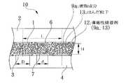
この例の電子部品の実装構造10は、図1及び図2に示すように、表面の全領域に複数のチップ側電極端子1が配設された半導体チップ(第1の電子部品又は基板)2と、チップ側電極端子1に対応した複数の基板側電極端子3が表面の全領域に配設されたパッケージ基板(第2の電子部品)4とが、両電極端子1、3が対向するように配置されて、対応する電極端子1、3同士がはんだバンプ5を介して接続されている構成において、半導体チップ2及びパッケージ基板4の対向面にそれぞれチップ側電極端子1及び基板側電極端子3に隣接するように複数のチップ側ダミー電極6及び基板側ダミー電極7が配設されて、これらのチップ側ダミー電極6及び基板側ダミー電極7には、有用なはんだバンプ5以外の過剰なはんだが吸着されて、ダミーバンプ8、及び未接合ダミーバンプ8A、8Bが形成されている。ここで、各ダミー電極6、7と、各電極端子1、3とは電気的に絶縁して配設されている。1 is a plan view showing the configuration of a mounting structure for an electronic component according to
As shown in FIGS. 1 and 2, the electronic
また、半導体チップ2とパッケージ基板4との間の空隙には樹脂層(導電性接着材12の絶縁性の樹脂成分)9が充填されている。このように、樹脂層9を充填することにより、半導体チップ2及びパッケージ基板4間の絶縁性を確保することができると共に、半導体チップ2の表面に配設されているチップ側電極端子1同士及びパッケージ基板4の表面に配設されている基板側電極端子3同士の絶縁性を確保することができる。さらに、半導体チップ2の内部に形成されている回路素子や、半導体チップ2及びパッケージ基板4の接合面に配設されている電極端子1、3等の構成要素を、実装構造10の外部雰囲気から保護することができる。 A gap between the
なお、図1は、図2の半導体チップ2を搭載する前のパッケージ基板4の表面(半導体チップ搭載面)の基板側電極端子3及び基板側ダミー電極7の配設パターンを示し、符号11は半導体チップ2が搭載される領域(すなわち、半導体チップ2とパッケージ基板4とが相互に重なり合って当接される領域、この明細書では、重合当接領域ともいう)を示している。また、パッケージ基板4の裏面に配設される第3の電極端子及びこの第3の電極端子に接続されるべき他のはんだバンプ、さらに半導体チップ2及びパッケージ基板4の周囲部分を覆うべきパッケージ樹脂体は、図示を省略している。 1 shows an arrangement pattern of the substrate-
パッケージ基板4の表面の基板側電極端子3は、例えば、直径が0.1mmの円形状の導電体が0.2mmの等間隔で格子状に配設されている。また、基板側ダミー電極7は、例えば、直径が0.08mm(基板側電極端子3より面積が小さくなるように)の円形状の導電体が、最近接して配設されている4つの基板側電極端子3で囲まれる領域のすべてに等間隔で格子状に配設されている。半導体チップ2の表面のチップ側電極端子1及びチップ側ダミー電極6も、それぞれパッケージ基板4の表面の基板側電極端子3及び基板側ダミー電極7と同一寸法及び同一間隔で格子状に配設されている。 The substrate-
後述の電子部品の実装方法でも説明するように、対応する電極端子1、3同士を接続するはんだバンプ5、各ダミー電極6、7に吸着されているダミーバンプ8は、半導体チップ2の搭載前にパッケージ基板4の表面に供給される導電性接着材12に予め含有されている、例えば、直径が5〜30μm、体積含有率が20−40%、この例では、30%の錫・インジウム共晶合金(融点:117℃)のはんだ粒子13が加熱(例えば、130−150℃)により溶融、凝集、一体化することにより形成される。また、半導体チップ2とパッケージ基板4との間の空隙に充填されている樹脂層9は、同様に導電性接着材12に予め含有されている樹脂成分が加熱(例えば、130−200℃)により硬化することにより形成される。 As will be described in the electronic component mounting method described later, the solder bumps 5 that connect the
上述したような電子部品の実装構造10によれば、供給される導電性接着材12に含有されるはんだ粒子13の量が過剰な場合でも、この過剰なはんだ粒子13はダミー電極6、7に吸着されて両電極端子6、7と金属接合するので、この過剰なはんだ粒子13が半導体チップ2及びパッケージ基板4間の樹脂層9中に残留することはない。ただし、過剰なはんだ粒子13の量によっては、必ずしも、相対向する2つのダミー電極6、7の両方に吸着されないでいずれか一方のみに吸着される場合もある。例えば、図2において、ダミーバンプ8は、過剰なはんだ粒子13の量が多いので、相対向する2つのダミー電極6、7の両方に吸着されて、さらに、凝集成長した、はんだ粒子同士が互いに接合することにより形成される。一方、未接合ダミーバンプ8A、8Bは、過剰なはんだ粒子13が少ないので、相対向する2つの電極6、7の両方に吸着されて、さらに、凝集成長しても、2つの凝集はんだ粒子同士が、接合には至らないものである。このような場合でも、過剰なはんだ粒子は完全に一方の電極端子と金属接合するので、樹脂層9中に残留することはない。したがって、過剰なはんだによる端子間ブリッジの発生を防止できるため、対応する電極端子1、3同士を確実に電気的に接続することができるので、実装構造の信頼性の向上を図ることができる。 According to the electronic
また、各ダミー電極6、7は、最もはんだ粒子13が残留し易い電極端子1、3から等距離の位置に配設することが望ましく、これに加えて前述したようにダミー電極6、7の面積を電極端子1、3のそれよりも小さくなるように設定することにより、ダミー電極6、7で過剰なはんだ粒子13を吸着する場合の吸着力を、隣接する電極端子1、3と差をつけることができるようになるので、各電極端子1、3及び各ダミー電極6、7間のブリッジの発生を防止することができるようになる。 The
また、ダミー電極6、7の設計にあたっては、ダミー電極6、7の大型化に伴って向上するはんだ粒子13の吸着能力と、電極端子1、3とダミー電極6、7とが過度に接近することにより発生する端子間ブリッジを考慮する必要がある。この点で、図3に示すように、電極端子1、3の直径をD、ダミー電極6,7の直径をd、電極端子1、3のピッチをLとすると、d<(L−D)×0.5の関係を満足するように選ぶことが望ましい。これによって、電極端子1、3とダミー電極6、7に吸着されたはんだ粒子13がブリッジすることなく良好な接合状態を実現することができる。また、半導体チップ2とパッケージ基板4とのギャップHについては、はんだ粒子13の直径(上述の例では5〜30μm)の3倍以上、望ましくは5倍以上に選ぶのが望ましい。これによって、加熱時のはんだ粒子13の動きが損なわれることなく、はんだ粒子13同士の凝集、一体化の動きが円滑に行われる。 In designing the
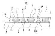
図4〜図6は、この例の電子部品の実装構造10で用いるダミー電極の配設パターンの変形例を示す断面図である。第1の変形例によるダミー電極の配設パターンは、図4に示すように、半導体チップ2及びパッケージ基板4のうち、一方のパッケージ基板4の表面のみに基板側電極端子3に隣接して基板側ダミー電極7を配設した例を示すものである。この基板側ダミー電極7には過剰なはんだが吸着されて未接合ダミーバンプ8Bが形成される。第2の変形例によるダミー電極の配設パターンは、図5に示すように、半導体チップ2及びパッケージ基板4の表面にそれぞれ対向して配設されるチップ側ダミー電極6と基板側ダミー電極7とのうち、チップ側ダミー電極6の面積を基板側ダミー電極7のそれよりも小さく配設した例を示すものである。同じチップ側ダミー電極6であっても、配設位置の違い及びはんだ粒子の量によってダミーバンプ8が形成されたり、未接合ダミーバンプ8A、8Bが形成されるようになる。第3の変形例によるダミー電極の配設パターンは、図6に示すように、半導体チップ2及びパッケージ基板4の表面にそれぞれ対向して配設される同じ面積のダミー電極6、7を、上下位置をずらして配設した例を示すものである。この第3の変形例では、第2の変形例と略同様に、面積が同じのダミー電極6、7であっても、配置位置の違い及びはんだ粒子の量によって形状の異なるダミーバンプ8、及び未接合ダミーバンプ8A、8Bが形成されるようになる。 4 to 6 are cross-sectional views showing modifications of the dummy electrode arrangement pattern used in the electronic
上述したような各変形例によるダミー電極の配設パターンによれば、電極端子1、3に隣接して配設するチップ側ダミー電極6又は基板側ダミー電極7の配設位置及び配設面積等を変化させて、チップ側ダミー電極6又は基板側ダミー電極7に吸着される過剰なはんだ粒子13の量を制御することができるので、用いるはんだ粒子の量に応じたダミー電極の配設パターンを選ぶことができる。 According to the dummy electrode arrangement pattern according to the above-described modifications, the arrangement position and area of the chip-
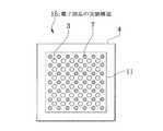
図7は、この例の電子部品の実装構造10で用いるダミー電極の形状の変形例を示す平面図である。第1の変形例によるダミー電極の形状は、図7(a)に示すように、格子状に等間隔で配設された4つの円形の基板側電極端子3(あるいは、チップ側電極端子1)の各電極端子3間に挟まれるように4つの円形の基板側ダミー電極7(あるいは、チップ側ダミー電極6)が配設された例を示し、第2の変形例によるダミー電極の形状は、図7(b)に示すように、格子状に等間隔で配設された4つの円形の基板側電極端子3で囲まれた領域の中央に1つの円形の基板側ダミー電極7が配設された例を示している。また、第3の変形例によるダミー電極の形状は、図7(c)に示すように、格子状に等間隔で配設された4つの円形の基板側電極端子3で囲まれた領域の中央に1つの方形の基板側ダミー電極7が配設された例を示し、第4の変形例によるダミー電極の形状は、図7(d)に示すように、格子状に等間隔で配設された4つの円形の基板側電極端子3で囲まれた領域の中央に1つのテトラポット形の基板側ダミー電極7が配設された例を示している。また、第5の変形例によるダミー電極の形状は、図7(e)に示すように、三角状に等間隔で配設された3つの円形の基板側電極端子3で囲まれた領域の中央に1つの円形の基板側ダミー電極7が配設された例を示し、第6の変形例によるダミー電極の形状は、図7(f)に示すように、三角状に等間隔で配設された3つの円形の基板側電極端子3で囲まれた領域の中央に1つの三角形の基板側ダミー電極7が配設された例を示している。 FIG. 7 is a plan view showing a modification of the shape of the dummy electrode used in the electronic
ここで、電極端子1、3及びダミー電極6、7に吸着されたはんだ粒子は、一体化して基本的にその表面エネルギーが最小になるような形になろうとする性質がある。すなわち、円形の各ダミー電極6、7に吸着されたはんだ粒子は球の一部の形状になろうとする。そこでその性質を利用して、各ダミー電極6、7の形状が隣接する各電極端子1、3の中央に向かう方向において、上述の各変形例によるダミー電極の形状のように、曲率半径がより小さな形状になるように選ぶことで、各ダミー電極6、7上に吸着されたはんだ粒子も各電極端子1、3への方向に対して比較的鋭角な形状になる。その結果、各電極端子1、3及び各ダミー電極6、7間をブリッジするはんだ形状の表面エネルギーを高めることができるので、ブリッジの発生を抑えることができるようになる。 Here, the solder particles adsorbed on the
このように、この例の電子部品の実装構造10によれば、表面の全領域に複数のチップ側電極端子1が配設された半導体チップ2と、チップ側電極端子1に対応した複数の基板側電極端子3が表面の全領域に配設されたパッケージ基板4とが、両電極端子1、3が対向するように配置されて、対応する電極端子1、3同士がはんだバンプ5を介して接続されている構成において、半導体チップ2及びパッケージ基板4の対向面にそれぞれチップ側電極端子1及び基板側電極端子3に隣接するように複数のチップ側ダミー電極6及び基板側ダミー電極7が配設されて、これらのダミー電極6、7には有効なはんだバンプ5以外の過剰なはんだが吸着されて、ダミーバンプ8、及び未接合ダミーバンプ8A、8Bが形成されているので、供給されるはんだの量が過剰な場合でも、この過剰なはんだはダミー電極6、7に吸着されるため、この過剰なはんだが樹脂層9中に残留することはない。
したがって、半導体チップ2とパッケージ基板4との対向する電極間を確実に電気的に接続して、信頼性の向上を図ることができる。Thus, according to the electronic
Therefore, it is possible to reliably connect the opposing electrodes of the
次に、図8(a)、(b)を参照して、この例の電子部品の実装構造10を得るための電子部品の実装方法について、工程順に説明する。
まず、図8(a)に示すように、表面に基板側電極端子3及び基板側ダミー電極7が配設されたパッケージ基板4を用意する。次に、パッケージ基板4の表面にメタルマスク(図示せず)を使用して、印刷法により厚さが50〜100μmの導電性接着材12を供給する。この導電性接着材12は、エポキシ系樹脂をベースとして、その中にフラックス活性作用を有する剤及びはんだ粒子13を含有させたものを用いる。フラックス活性作用を有する剤としては、(メタ)アクリル酸、マレイン酸等の不飽和酸、蓚酸、マロン酸等の有機二酸、クエン酸等の有機酸をはじめとして、トリメリット酸、テトラメリット酸及びキレート剤等を少なくとも一つ有しているものを用いる。はんだ粒子13としては、例えば、錫・インジウム共晶合金(融点:117℃)からなる粒径が5〜30μm、体積含有率が30%のものを用いる。錫・インジウム共晶合金の他に、銀、銅、ビスマス、アンチモン等からなる2元系、又は3元系のはんだ合金を用いても良い。ただし、はんだ粒子が凝集、一体化の挙動をするには、はんだが溶融する温度において導電性接着材12の樹脂成分の粘度が低く抑えられている必要がある。したがって、はんだ材料の選定にあたっては、接合性の面からは低融点であることが望ましい。Next, an electronic component mounting method for obtaining the electronic
First, as shown in FIG. 8A, a
ここで、次の工程である半導体チップ2の搭載時のエア巻き込みを防止するため、また導電性接着材12の半導体チップ2表面への濡れ広がりの起点となるように、導電性接着材12あるいはその樹脂成分のみを半導体チップ2に、又はスキージング後のパッケージ基板4の搭載面の少なくとも一方の搭載面上にポッティング法等により供給しても良い。また、導電性接着材12は薄く延ばして乾燥させてフィルム状にしたものをパッケージ基板4の表面に貼り付けるようにしても良い。さらにフィルム状にしたものはタック性を持たせるか、あるいは供給後のフィルム上に微量の導電性接着材、あるいはその樹脂成分のみをポッティング法等により供給しても良い。 Here, in order to prevent air entrainment at the time of mounting the
次に、図8(b)に示すように、搭載機を用いてチップ側電極端子1及び基板側電極端子3が対向するように位置合わせした後、パッケージ基板4上に半導体チップ2を搭載する。この搭載はパッケージ基板4と半導体チップ2とのギャップが所定の値となるように制御して、側面から導電性接着材12の半導体チップ2側への全面濡れ広がりを確認し、必要に応じて両者2、4間のギャップを微調整する。またフィルム状のものを用いた場合には、荷重制御により半導体チップ2をパッケージ基板4に搭載しても良い。 Next, as shown in FIG. 8B, after positioning so that the chip-
次に、一体化された半導体チップ2及びパッケージ基板4を、搭載機の加熱ヘッドによって加熱する。加熱プロファイルは、接合部を117〜180℃の範囲で昇温して加熱し、その状態で10秒間以上保持するように設定して、その後半導体チップ2及びパッケージ基板4を搭載機から取り外す。続いて、半導体チップ2及びパッケージ基板4をベーク炉内に搬送して、100℃で30分間以上加熱して、導電性接着材12の樹脂成分の硬化を行って、図2に示したような電子部品の実装構造10を完成させる。 Next, the
上述したような電子部品の実装方法によれば、基板側電極端子3及び基板側ダミー電極7が配設されたパッケージ基板4の、チップ側電極端子1及びチップ側ダミー電極6が配設された半導体チップ2との対向面に少なくともはんだ粒子13及び樹脂成分を含有した導電性接着材12を供給し、電極端子1、3が対向するように位置合わせして、パッケージ基板4上に半導体チップ2を搭載した後、加熱して導電性接着材12のはんだ粒子13を溶融、凝集、一体化させて対応する電極端子1、3同士をはんだバンプ5を介して接続すると同時に、過剰なはんだをダミー電極6、7に吸着させてダミーバンプ8、及び未接合ダミーバンプ8A、8Bを形成するので、簡単な工程の組合せで、予め半導体チップ2やパッケージ基板4上にバンプを形成する必要がなく、かつフラックス洗浄を不要にして、過剰なはんだを吸着するダミー電極を備えた電子部品の実装構造を得ることができる。 According to the electronic component mounting method as described above, the chip-
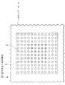
図9は、この発明の実施例2である電子部品の実装構造の構成を示す平面図である。この例の電子部品の実装構造の構成が、上述の実施例1のそれと大きく異なるところは、電極端子の外側にもダミー電極を配設するようにした点である。なお、この例の電子部品の実装構造では、半導体チップを省略して示している。
この例の電子部品の実装構造15は、図9に示すように、パッケージ基板4の表面(半導体チップ搭載面)には、最も外側に配設されている複数の基板側電極端子3のさらに外側に隣接するように複数の基板側ダミー電極7が配設されている。また、パッケージ基板4上に搭載されるべき半導体チップ(図示せず)の表面のチップ側電極端子1及びチップ側ダミー電極6も、それぞれパッケージ基板4の表面の基板側電極端子3及び基板側ダミー電極7と同様なレイアウトで配設されている。これ以外は、前述した実施例1の構成と略同様であるので、詳細な説明は省略する。FIG. 9 is a plan view showing the configuration of the electronic component mounting structure according to the second embodiment of the present invention. The configuration of the electronic component mounting structure of this example is greatly different from that of the first embodiment described above in that a dummy electrode is disposed outside the electrode terminal. In the electronic component mounting structure of this example, the semiconductor chip is omitted.
As shown in FIG. 9, the electronic component mounting structure 15 in this example is provided on the front surface (semiconductor chip mounting surface) of the
上述したような電子部品の実装構造15によれば、半導体チップ2及びパッケージ基板4にそれぞれ配設される各電極端子1、3のうち、最も外側に配設されている各電極端子1、3のさらに外側に隣接するように、ダミー電極6、7が配設されるので、特に最も外側に配設されている各電極端子1、3が接続領域の端部から内側に離れて配置されている場合において、過剰なはんだが各ダミー電極6、7に吸着されることにより、それらの各電極端子1、3に形成されるはんだバンプが過剰に大きくなるのを防止することができる。また、外側に配設するダミー電極6、7の数あるいは列数を適宜増減することにより、隣接している各電極端子1、3の周辺部に存在している過剰なはんだを確実に各ダミー電極6、7に吸着させることができる。 According to the electronic component mounting structure 15 as described above, the
このように、この例の電子部品の実装構造15によっても、各電極端子1、3の外側にも各ダミー電極6,7を配設するようにしたので、実施例1と略同様な効果得ることができる。 As described above, since the
図10は、この発明の実施例3である電子部品の実装構造の構成を示す平面図である。この例の電子部品の実装構造の構成が、上述の実施例1のそれと大きく異なるところは、第1の電子部品又は基板としてBGA(Ball Grid Array)形パッケージを用いて、第2の電子部品又は基板としてのマザーボード上に実装するようにした点である。なお、この例の電子部品の実装構造では、BGA形パッケージを省略して示している。
この例の電子部品の実装構造20は、図10に示すように、マザーボード16の表面(BGA形パッケージ搭載面)の外周部には基板側電極端子3が配設されて、この基板側電極端子3は、例えば、直径が0.25mmの円形状の導電体が0.5mmの等間隔で格子状に配設されている。また、マザーボード16の表面の中央部には、基板側ダミー電極7が、基板側電極端子3と同一寸法及び同一間隔で格子状に配設されている。これによって、マザーボード16の表面の外周部に配設された基板側電極端子3の配置密度と、その表面の中央部に配設された基板側ダミー電極7の配置密度とは同じになっている。また、マザーボード16上に搭載されるBGA形パッケージ(図示せず)の表面のチップ側電極端子1及びチップ側ダミー電極6も、それぞれマザーボード16の表面の基板側電極端子3及び基板側ダミー電極7と同様なレイアウトで配設されている。FIG. 10 is a plan view showing the configuration of the electronic component mounting structure according to
As shown in FIG. 10, the electronic component mounting structure 20 of this example is provided with substrate-
この例では、実施例1におけるチップ側電極端子1と基板側電極端子3とを接続するためのはんだバンプ5、ダミー電極6、7に吸着されるダミーバンプ8に相当する各はんだバンプは、BGA形パッケージの搭載前にマザーボード16の表面に供給される導電性接着材に予め含有されている、例えば、直径が20〜40μmの錫・ビスマス共晶合金(融点:139℃)のはんだ粒子を加熱により溶融、凝集、一体化することにより形成する。 In this example, each solder bump corresponding to the
この例の電子部品の実装方法では、マザーボード16上にBGA形パッケージを搭載した後、両者を上下赤外線加熱のリフロー炉に搬送して、錫・ビスマス共晶合金の融点とプロセスタイムの短縮を加味して2ステップで加熱する。具体的には、第1のステップとして、錫・ビスマス共晶合金の融点(139℃)以上の150℃で10秒間以上加熱して、はんだ粒子を溶融、凝集、一体化させる。次に、第2のステップとして、180℃で30秒間以上加熱して、樹脂成分を硬化させて、電子部品の実装構造20を完成させる。 In this example of electronic component mounting method, after mounting a BGA package on the
上述したような電子部品の実装構造20によれば、マザーボード16及びBGA形パッケージの表面の中央部にはダミー電極6、7が配設されているので、過剰なはんだはこれらのダミー電極6,7に吸着されるようになる。したがって、マザーボード16及びBGA形パッケージの対向面の外周部に配設されている電極端子1、3間を接続するためのはんだバンプは、均一な量が凝集されて形成されるようになる。 According to the electronic component mounting structure 20 as described above, the
このように、この例の電子部品の実装構造20によっても、第1の電子部品又は基板と第2の電子部品又は基板との組合せが異なるだけで、実施例1と略同様な効果を得ることができる。 As described above, the electronic component mounting structure 20 of this example also obtains substantially the same effect as that of the first embodiment, except that the combination of the first electronic component or substrate and the second electronic component or substrate is different. Can do.
図11は、この発明の実施例4である電子部品の実装構造の構成を示す平面図である。この例の電子部品の実装構造の構成が、上述の実施例3のそれと大きく異なるところは、BGA形パッケージ(第1の電子部品又は基板)とマザーボード(第2の電子部品又は基板)との組合せにおいて、ダミー電極の配設パターンを変更した点である。
この例の電子部品の実装構造25は、図11に示すように、マザーボード16の表面のみに、その最近接して配設されている4つの基板側電極端子3で囲まれる領域のすべてに、直径が0.2mmの円形状の導電体からなる基板側ダミー電極17が等間隔で格子状に配設されている。すなわち、ダミー電極17を配設した分だけ、マザーボード16の方がBGA形パッケージのダミー電極よりも多くなっている。これ以外は、前述した実施例3の構成と略同様であるので、詳細な説明は省略する。FIG. 11 is a plan view showing the configuration of the electronic component mounting structure according to
As shown in FIG. 11, the electronic component mounting structure 25 of this example has a diameter in all of the area surrounded by the four board-
上述したような電子部品の実装構造25によれば、マザーボード16のみの表面には、最近接して配設されている4つの基板側電極端子3で囲まれる領域のすべてに、基板側ダミー電極17が等間隔で格子状に配設されているので、基板側ダミー電極17を配設した分だけ、過剰なはんだに対するダミー電極17の吸着能力を高めることができる。したがって、マザーボード16の全領域における端子間ブリッジを防止することができ、その全領域において各電極端子1、3間を確実に電気的に接続することができるようになる。また、加熱プロセスについては実施例3と同様に行うことができる。ただし、この例では、ダミー電極17をマザーボード16のみに配設していることにより、リフロー炉による加熱時は上下のヒータ−ブロックの温度設定に差をつけてマザーボード16側をより高温にすることで、ダミー電極17へのはんだの凝集を適宜促進することが望ましい。 According to the electronic component mounting structure 25 as described above, the board-side dummy electrode 17 is provided on the entire surface surrounded by the four board-
このように、この例の電子部品の実装構造25によっても、マザーボード16のみにより多くのダミー電極17を配設することにより、実施例3と略同様な効果を得ることができる。 As described above, the electronic component mounting structure 25 of this example can provide substantially the same effect as that of the third embodiment by disposing more dummy electrodes 17 only on the
以上、この発明の実施例を図面により詳述してきたが、具体的な構成はこの実施例に限られるものではなく、この発明の要旨を逸脱しない範囲の設計の変更等があってもこの発明に含まれる。例えば、ダミー電極は、必要に応じて、個数を増減でき、少なくとも1個あれば良い場合もありうる。また、電子部品の電極端子の配置密度が一様でなくて、外周部のみに配設されて中央部には配設されていないような場合は、この中央部にダミー電極を電極端子と同じ配置密度で配設することにより、中央部におけるはんだ粒子の残留を防止することができる。また、電極端子が疎密のある配置密度で配設されている場合には、疎な配置密度で配設されている電極端子に隣接してダミー電極を配設することにより、より確実にはんだ粒子の残留を防止することができる。要するに、接合面のうち、電極端子が密に配列された密な領域よりも、電極端子が疎に配列された疎な領域の方が、ダミー電極の配置密度が高くなるように設定するのが好ましい。つまり、電極端子にダミー電極を含む全体としての電極密度を均等化する態様で、ダミー電極を配列するのが好ましい。 The embodiment of the present invention has been described in detail with reference to the drawings. However, the specific configuration is not limited to this embodiment, and the present invention can be changed even if there is a design change or the like without departing from the gist of the present invention. include. For example, the number of dummy electrodes can be increased or decreased as necessary, and at least one dummy electrode may be sufficient. In addition, when the arrangement density of the electrode terminals of the electronic component is not uniform and is disposed only in the outer peripheral portion but not in the central portion, the dummy electrode is the same as the electrode terminal in the central portion. By arranging with the arrangement density, it is possible to prevent the solder particles from remaining in the central portion. In addition, when the electrode terminals are arranged with a sparse arrangement density, solder particles are more reliably arranged by arranging a dummy electrode adjacent to the electrode terminals arranged with a sparse arrangement density. Can be prevented from remaining. In short, it is set so that the arrangement density of the dummy electrodes is higher in the sparse region in which the electrode terminals are sparsely arranged than in the dense region in which the electrode terminals are densely arranged in the bonding surface. preferable. That is, it is preferable to arrange the dummy electrodes in a manner that equalizes the overall electrode density including the dummy electrodes in the electrode terminals.
また、実施例では、第1の電子部品又は基板と第2の電子部品又は基板との組み合せは、半導体チップとパッケージ基板あるいはBGA形パッケージとマザーボードとの組み合せ例で説明したが、これに限らずに半導体チップと半導体チップとの組み合せ例、いわゆるCoC(Chip on Chip)実装構造等の他の組み合せ例にも適用することができる。また、第1の電子部品又は基板としては半導体チップを組み込んだ半導体パッケージにも適用することでき、さらに、この半導体パッケージ同士を組み合せてもよく、あるいは上記のBGA形パッケージ同士を組み合せても良い。また、半導体チップ、BGA形パッケージ、半導体パッケージ等を第1の電子部品又は基板として用いてこれらを実装する第2の電子部品又は基板としては、実施例で示したパッケージ基板、マザーボード等に限らずに、通常配線基板やプリント配線基板等として呼称されている基板全体に適用することができる。また、実施例では、ダミー電極が電極端子よりも面積が小さい例で説明したが、これに限らず逆な関係となるように各電極端子を配設することもできる。例えば、電極端子が疎密のある配置密度で配設されている場合には、周囲スペースに余裕がある疎な配置密度で配設されている電極端子に隣接して大きな面積のダミー電極を配設することにより、過剰なはんだの吸着能力をより大きくすることができる。また、実施例で示した各電極端子の寸法、間隔等の具体的数値、導電体材料、導電性接着材、はんだ粒子等の具体的材料、各電極端子の配設パターン、ダミー電極の形状等は一例を示したものであって、目的、用途等に応じて適宜変更することができる。 In the embodiment, the combination of the first electronic component or substrate and the second electronic component or substrate has been described as an example of a combination of a semiconductor chip and a package substrate or a BGA type package and a motherboard. However, the present invention is not limited to this. In addition, the present invention can also be applied to other combinations such as a combination example of a semiconductor chip and a semiconductor chip, such as a so-called CoC (Chip on Chip) mounting structure. Further, the first electronic component or the substrate can be applied to a semiconductor package in which a semiconductor chip is incorporated, and the semiconductor packages may be combined with each other, or the BGA type packages may be combined with each other. In addition, the second electronic component or the substrate on which the semiconductor chip, the BGA type package, the semiconductor package or the like is mounted as the first electronic component or the substrate is not limited to the package substrate or the motherboard shown in the embodiment. In addition, the present invention can be applied to the entire substrate generally called as a wiring board or a printed wiring board. In the embodiment, the dummy electrode has been described as having an area smaller than that of the electrode terminal. For example, if the electrode terminals are arranged with a sparse and dense arrangement density, a dummy electrode with a large area is arranged adjacent to the electrode terminals arranged with a sparse arrangement density with a margin in the surrounding space. By doing so, the adsorption capability of excess solder can be further increased. Also, specific values such as dimensions and intervals of each electrode terminal shown in the examples, specific materials such as conductor material, conductive adhesive, solder particles, arrangement pattern of each electrode terminal, shape of dummy electrode, etc. Is an example, and can be appropriately changed according to the purpose, application, and the like.
1 チップ側電極端子(第1の電極端子)
2 半導体チップ(第1の電子部品又は基板)
3 基板側電極端子(第2の電極端子)
4 パッケージ基板(第2の電子部品又は基板)
5 はんだバンプ
6 チップ側ダミー電極(ダミー電極)
7、17 基板側ダミー電極(ダミー電極)
8 ダミーバンプ
8A、8B 未接合ダミーバンプ
9 樹脂層(樹脂成分)
10、15、20、25 電子部品の実装構造
11 半導体チップの搭載領域
12 導電性接着材
13 はんだ粒子
16 マザーボード1 Chip-side electrode terminal (first electrode terminal)
2 Semiconductor chip (first electronic component or substrate)
3 Substrate side electrode terminal (second electrode terminal)
4 Package substrate (second electronic component or substrate)
5
7, 17 Substrate side dummy electrode (dummy electrode)
8 Dummy bumps 8A, 8B Unbonded dummy bumps 9 Resin layer (resin component)
10, 15, 20, 25 Mounting structure of
Claims (3)
Translated fromJapanese前記第1の接合面又は/及び前記第2の接合面に、有効な電極端子としては機能しない少なくとも1個のダミー電極をさらに設け、
前記第1の接合面と前記第2の接合面とを相対向させ、これら第1及び第2の接合面に間に導電性接着材を挿入充填した後、
所定の加熱下で、前記導電性接着材に含有されるはんだ粒子を、前記第1の電極端子及び前記第2の電極端子のパッド面で、凝集、一体化させて、互いに対応関係のある前記第1の電極端子と第2の電極端子とをはんだ接続すると共に、前記はんだ粒子のうち、余分なはんだ粒子をダミー電極に吸着させることを特徴とする電子部品の実装方法。A first electronic component or substrate in which a plurality of first electrode terminals are arranged on the first bonding surface, and a second electronic component or substrate in which a plurality of second electrode terminals are arranged on the second bonding surface And joining the first joint surface and the second joint surface by inserting a conductive adhesive between the first joint surface and the second joint surface. And a mounting method of an electronic component for solder-connecting the first electrode terminal and the second electrode terminal that have a corresponding relationship to each other,
At least one dummy electrode that does not function as an effective electrode terminal is further provided on the first bonding surface or / and the second bonding surface,
After the first bonding surface and the second bonding surface are opposed to each other, and a conductive adhesive is inserted and filled between the first and second bonding surfaces,
Under predetermined heating, the solder particles contained in the conductive adhesive are aggregated and integrated on the pad surfaces of the first electrode terminal and the second electrode terminal, and have a corresponding relationship with each other. A method for mounting an electronic component, wherein the first electrode terminal and the second electrode terminal are solder-connected, and extra solder particles among the solder particles are adsorbed to a dummy electrode.
Priority Applications (1)
| Application Number | Priority Date | Filing Date | Title |
|---|---|---|---|
| JP2006253316AJP4887997B2 (en) | 2006-09-19 | 2006-09-19 | Electronic component mounting method |
Applications Claiming Priority (1)
| Application Number | Priority Date | Filing Date | Title |
|---|---|---|---|
| JP2006253316AJP4887997B2 (en) | 2006-09-19 | 2006-09-19 | Electronic component mounting method |
Publications (2)
| Publication Number | Publication Date |
|---|---|
| JP2008078238A JP2008078238A (en) | 2008-04-03 |
| JP4887997B2true JP4887997B2 (en) | 2012-02-29 |
Family
ID=39350029
Family Applications (1)
| Application Number | Title | Priority Date | Filing Date |
|---|---|---|---|
| JP2006253316AExpired - Fee RelatedJP4887997B2 (en) | 2006-09-19 | 2006-09-19 | Electronic component mounting method |
Country Status (1)
| Country | Link |
|---|---|
| JP (1) | JP4887997B2 (en) |
Families Citing this family (8)
| Publication number | Priority date | Publication date | Assignee | Title |
|---|---|---|---|---|
| JP2008198745A (en)* | 2007-02-09 | 2008-08-28 | Sumitomo Bakelite Co Ltd | Solder bump forming method, solder bump, semiconductor device and manufacturing method of semiconductor device |
| JP5560713B2 (en)* | 2007-10-05 | 2014-07-30 | 日本電気株式会社 | Electronic component mounting method, etc. |
| JP5264585B2 (en) | 2009-03-24 | 2013-08-14 | パナソニック株式会社 | Electronic component joining method and electronic component |
| KR101711499B1 (en) | 2010-10-20 | 2017-03-13 | 삼성전자주식회사 | Semiconductor package and method of forming the same |
| JP2013251562A (en)* | 2013-07-22 | 2013-12-12 | Sumitomo Bakelite Co Ltd | Conductive connection material with dicing sheet function, connection method between terminals, and electrical and electronic components |
| JP6588214B2 (en)* | 2015-03-19 | 2019-10-09 | 新光電気工業株式会社 | Electronic component device and method of manufacturing electronic component device |
| DE102017128568A1 (en)* | 2017-12-01 | 2019-06-06 | Infineon Technologies Ag | SEMICONDUCTOR CHIP WITH A VARIETY OF EXTERNAL CONTACTS, CHIP ARRANGEMENT AND METHOD FOR CHECKING AN ORIENTATION OF A POSITION OF A SEMICONDUCTOR CHIP |
| JP7397589B2 (en)* | 2019-06-28 | 2023-12-13 | エルジー ディスプレイ カンパニー リミテッド | Electronic device and its manufacturing method, and display device and its manufacturing method |
Family Cites Families (6)
| Publication number | Priority date | Publication date | Assignee | Title |
|---|---|---|---|---|
| JP3169254B2 (en)* | 1992-03-18 | 2001-05-21 | 株式会社日立製作所 | Multilayer wiring board |
| JPH10308413A (en)* | 1997-05-07 | 1998-11-17 | Casio Comput Co Ltd | Electronic components and electronic component mounting modules |
| JP2000165007A (en)* | 1998-11-27 | 2000-06-16 | Nec Corp | Printed circuit board, electronic component and its mounting method |
| JP2001257289A (en)* | 2000-03-10 | 2001-09-21 | Mitsubishi Electric Corp | Semiconductor package, semiconductor device, and method of manufacturing semiconductor device |
| JP2003017530A (en)* | 2001-06-28 | 2003-01-17 | Hitachi Ltd | Semiconductor device and mounting method thereof |
| JP2006245189A (en)* | 2005-03-02 | 2006-09-14 | Matsushita Electric Ind Co Ltd | Flip chip mounting method and mounting structure for semiconductor element |
- 2006
- 2006-09-19JPJP2006253316Apatent/JP4887997B2/ennot_activeExpired - Fee Related
Also Published As
| Publication number | Publication date |
|---|---|
| JP2008078238A (en) | 2008-04-03 |
Similar Documents
| Publication | Publication Date | Title |
|---|---|---|
| JP4887997B2 (en) | Electronic component mounting method | |
| US7482199B2 (en) | Self alignment features for an electronic assembly | |
| TWI549204B (en) | Manufacturing method of semiconductor device | |
| TWI419300B (en) | Electronic component built-in substrate and method of manufacturing electronic component built-in substrate | |
| TW200525666A (en) | Bump-on-lead flip chip interconnection | |
| CN1340851A (en) | Electronic device and its manufacture method | |
| JP5569676B2 (en) | Electronic component mounting method | |
| JP2009099669A (en) | Mounting structure of electronic component, and mounting method thereof | |
| KR102006637B1 (en) | Method Of Forming Bump And Semiconductor device including The Same | |
| JP4051570B2 (en) | Manufacturing method of semiconductor device | |
| JP2000277649A (en) | Semiconductor and manufacture of the same | |
| JP2004128056A (en) | Semiconductor device and manufacturing method thereof | |
| JP5560713B2 (en) | Electronic component mounting method, etc. | |
| JP3972209B2 (en) | Semiconductor device and manufacturing method thereof, circuit board, and electronic apparatus | |
| TWI508258B (en) | Semiconductor package and manufacturing method thereof | |
| CN101399246A (en) | Package substrate structure and production method thereof | |
| JP2008288490A (en) | Process for producing built-in chip substrate | |
| JP3847602B2 (en) | Stacked semiconductor device, method for manufacturing the same, motherboard mounted with semiconductor device, and method for manufacturing motherboard mounted with semiconductor device | |
| JP2007266564A (en) | Flip chip bonded package | |
| JP5245270B2 (en) | Semiconductor device and manufacturing method thereof | |
| JP4324773B2 (en) | Manufacturing method of semiconductor device | |
| JP5333220B2 (en) | Semiconductor device mounting structure and semiconductor device mounting method | |
| JP2016162813A (en) | Printed circuit board and soldering method | |
| JP2000133680A (en) | Surface mounting joint member | |
| JP4561969B2 (en) | Semiconductor device |
Legal Events
| Date | Code | Title | Description |
|---|---|---|---|
| A621 | Written request for application examination | Free format text:JAPANESE INTERMEDIATE CODE: A621 Effective date:20090812 | |
| A977 | Report on retrieval | Free format text:JAPANESE INTERMEDIATE CODE: A971007 Effective date:20110819 | |
| A131 | Notification of reasons for refusal | Free format text:JAPANESE INTERMEDIATE CODE: A131 Effective date:20110823 | |
| A521 | Written amendment | Free format text:JAPANESE INTERMEDIATE CODE: A523 Effective date:20111024 | |
| TRDD | Decision of grant or rejection written | ||
| A01 | Written decision to grant a patent or to grant a registration (utility model) | Free format text:JAPANESE INTERMEDIATE CODE: A01 Effective date:20111115 | |
| A01 | Written decision to grant a patent or to grant a registration (utility model) | Free format text:JAPANESE INTERMEDIATE CODE: A01 | |
| A61 | First payment of annual fees (during grant procedure) | Free format text:JAPANESE INTERMEDIATE CODE: A61 Effective date:20111128 | |
| R150 | Certificate of patent or registration of utility model | Free format text:JAPANESE INTERMEDIATE CODE: R150 | |
| FPAY | Renewal fee payment (event date is renewal date of database) | Free format text:PAYMENT UNTIL: 20141222 Year of fee payment:3 | |
| LAPS | Cancellation because of no payment of annual fees |